


Sony ICDV-21 Service manual
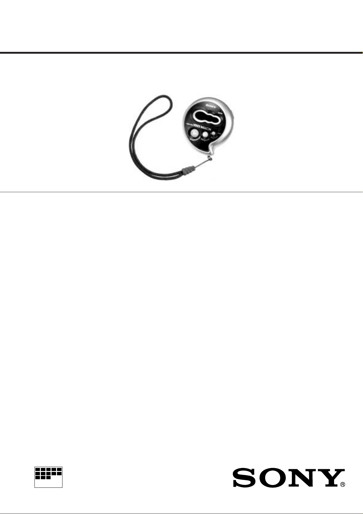
ICD-V21
SERVICE MANUAL
SPECIFICATIONS
Recording media Built-in flash memory
Recording time 10 minutes
Frequency response 200 Hz - 2,500 Hz
Speaker approx. 2.8 cm (11/8 in.) dia.
Power output 40 mw
Power requirements Two lithium batteries : 3V DC
Dimensions (w/h/d) (incl. projecting parts and controls)
Mass (including battery) Approx. 50g (1.8 oz)
Supplied accessories Hand strap (1)
Design and specifications are subject to change without notice.
US Model
Canadian Model
AEP Model
E Model
Tourist Model
approx. 62 × 67.5 × 23.5 mm (23/8 × 25/8 × 15/16 in.)
CR2032 lithium batteries (2)
MICROFILM
IC RECORDER

TABLE OF CONTENTS
SERVICING NOTE ······················································ 2
1. GENERAL ······································································ 3
2. DISASSEMBLY
2-1. MAIN board ·······································································4
3. DIAGRAMS
3-1. IC Block Diagrams ····························································· 5
3-2. Printed Wiring Board — MAIN Section — ······················· 6
3-3. Schematic Diagram — MAIN Section —··························9
3-4. IC Pin Functions ······························································· 12
4. EXPLODED VIEWS ·················································· 15
5. ELECTRICAL PARTS LIST ··································· 16
SERVICE NOTE
Notes on chip component replacement
• Never reuse a disconnected chip component.
• Notice that the minus side of a tantalum capacitor may be damaged
by heat.
Flexible Circuit Board Repairing
• Keep the temperature of soldering iron around 270 ˚C during
repairing.
• Do not touch the soldering iron on the same conductor of the
circuit board (within 3 times).
• Be careful not to apply force on the conductor when soldering or
unsoldering.
— 2 —
SECTION 1
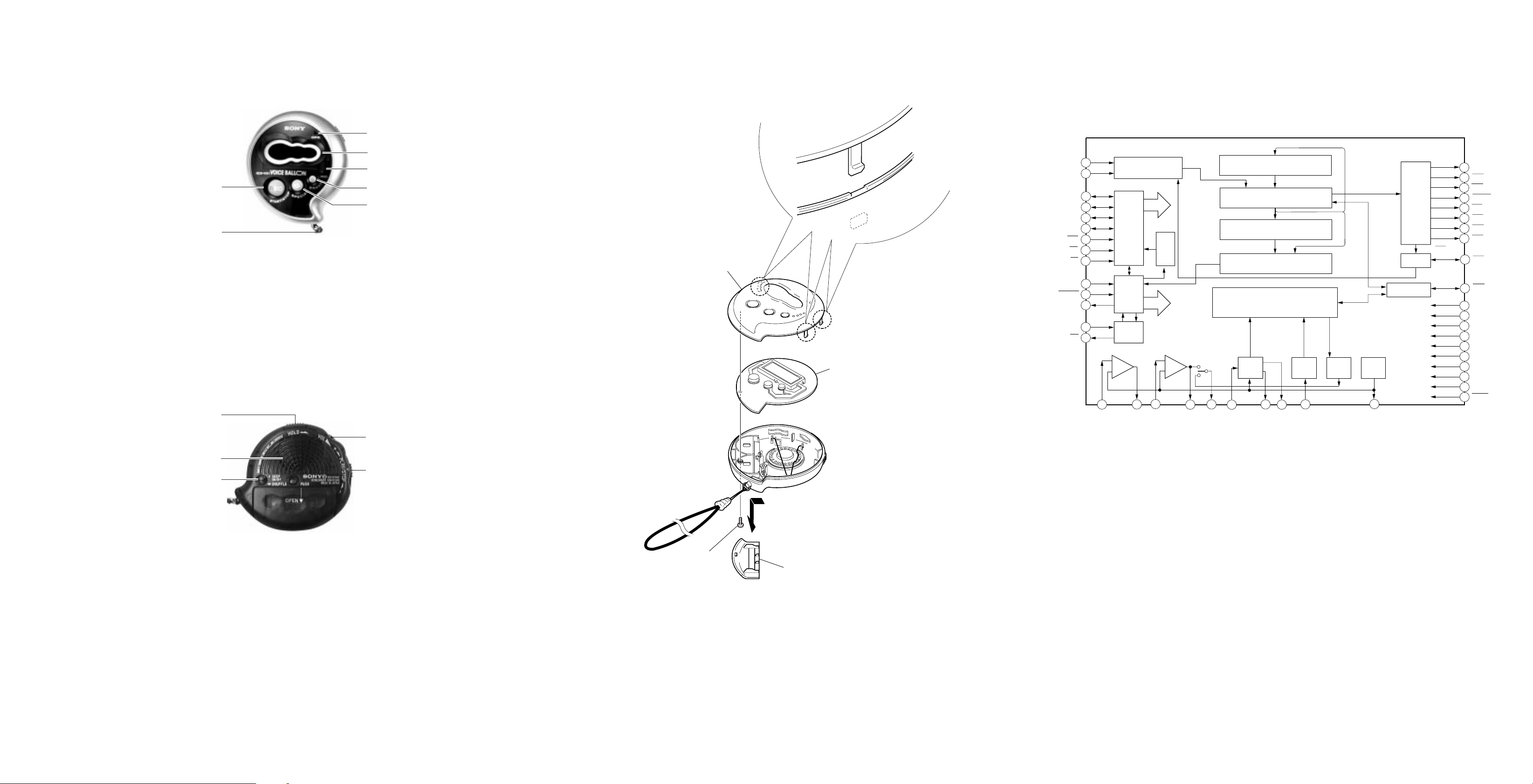
D3 10
D2
9
RSEL1
30
RSEL2
31
D1 8
D0
7
WR
1
RD
2
CE
3
MCUM
6
RESET
44
MON
42
XT
37
XT
38
MIN
22
MOUT
21
FIN
14
AOUT
13
FOUT
12
ADIN
11
SG
18
20 Stage
Address Counter
Address
Controller
DV
DD
39
DV
DD'
17
AV
DD
16
DGND24
AGND
23
TEST43
TEST
33
TEST
32
SAD
27
SAS
26
TAS
25
RWCK41
WE
40
CS1
28
CS2
29
CS3 (STBY)
34
CS4 (RSEL0)35
DI/O
36
TEST
4
TEST
5
OSC
LPF
_
+
Date I/O
I/O
CS4
20-bit
Address Register
20-bit
Stop Address Register
20-bit
Comparator
ADPCM
Analyzer/Synthsizer
Register
Contoroller
12 bit
DAC
12 bit
ADC
SG
Circuit
MCU I/F
Timing
Controller
Status
Register
LIN
20
LOUT19AMON
15
_
+
RSEL0
GENERAL
SECTION 2
DISASSEMBLY
SECTION 3
ICD-V21
DIAGRAMS
FRONT SIDE
7
6
1 REC/PB (OPB) LAMP
2 LCD window
3 Built-in MIC
4 ERASE button
1
2
3
4
5
5 SPECIAL MESSAGE button
6 Hand strap
7 REC START/STOP button
Note : Follow the disassembly procedure in the numerical order given.
2-1. MAIN board
Remove the three claws
3
Front panel assy
3-1. IC BLOCK DIAGRAMS
IC101 MSM6588LGS-2K
4
Main board
REAR SIDE
!™
8
!¡
9
!º
8 VOL knob
9 Jog lever
!º BEEP/SHUFFULE button
— 3 —
!¡ Speaker
!™ HOLD knob
2
Screw
(B 1.7
×
4)
1
Lid, battery case
— 4 —
— 5 —