

Page 1
ICD-SX68/SX68DR9/SX78/
SX78DR9/SX88
SERVICE MANUAL
Ver. 1.0 2008.02
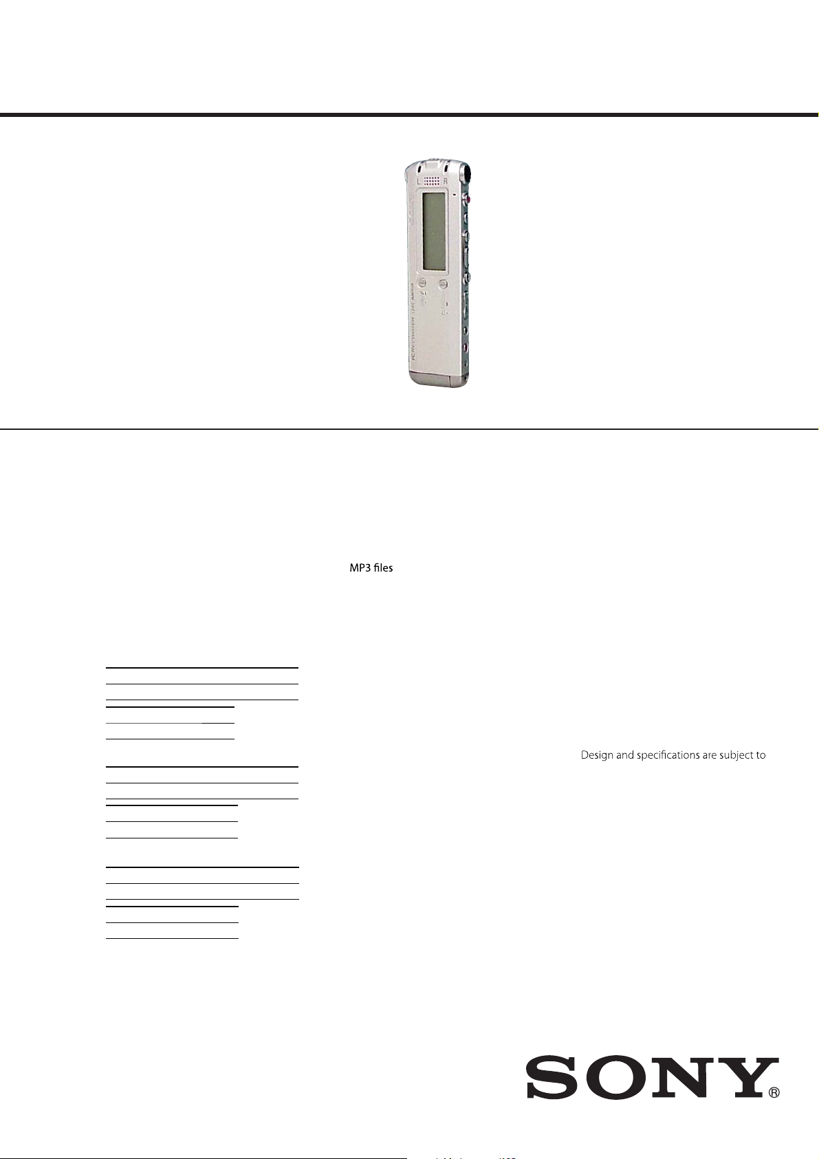
Photo : ICD-SX68
SPECIFICATIONS
Capacity (User available capacity)
ICD-SX68/SX68DR9: 512MB
(approx. 483MB=507,346,944Byte)
ICD-SX78/SX78DR9: 1GB
(approx. 975MB=1,022,590,976Byte)
ICD-SX88: 2GB
(approx. 1.93GB=2,081,521,664Byte)
A part of the memory capacity is used as a
management area.
Recording time
Maximum recording time
The maximum recording time of all the
folders is as follows.
ICD-SX68/SX68DR9
STHQ mode ST mode STLP mode
8 hr. 35 min. 22 hr. 50 min. 44 hr. 00 min.
SP mode LP mode
69 hr. 40 min. 185 hr. 55 min.
ICD-SX78/SX78DR9
STHQ mode ST mode STLP mode
17 hr. 25 min. 46 hr. 5 min. 88 hr. 45 min.
SP mode LP mode
140 hr. 35 min. 374 hr. 55 min.
ICD-SX88
STHQ mode ST mode STLP mode
35 hr. 30 min. 93 hr. 55 min. 180 hr. 45 min.
SP mode LP mode
286 hr. 10 min. 763 hr. 15 min.
(hr : hours/min. : minutes)
Frequency range
STHQ : 80 Hz - 20,000 Hz
•
ST : 80 Hz - 16,500 Hz
•
STLP : 80 Hz - 7,000 Hz
•
SP : 80 Hz - 6,000 Hz
•
LP : 80 Hz - 3,500 Hz
•
Bit rates and sampling frequencies for
Bit rate: 32 - 320 kbps, VBR
Sampling frequencies: 16/22.05/24/32/44.1/
48 kHz
Not all encoders are supported.
Speaker
Approx. 16 mm (21/32 in.) dia.
Power output
150 mW
Input/Output
Microphone jack (minijack, stereo)
•
input for plug in power, minimum input
–
level 0.6 mV, 3 kilohms or lower impedance
microphone
Headphone jack (minijack, stereo)
•
output for 8 - 300 ohms headphones
–
USB connector
•
Playback speed control
+200% to –75% (DPC)
Power requirements
Two NH-AAA rechargeable batteries: 2.4 V DC
Two LR03 (size AAA) alkaline batteries: 3.0 V DC
Operating temperature
5˚C - 35˚C (41˚F - 95˚F)
Dimensions (w/h/d) (not incl.
projecting parts and controls)(JEITA)*
30.8 × 119.3 × 14.9 mm (1 1/4 × 4 3/4 × 19/32
in.)
US Model
Canadian Model
ICD-SX68/SX68DR9
AEP Model
E Model
ICD-SX68/SX78/SX78DR9
Korea Model
ICD-SX68/SX78/SX88
Mass (JEITA)*
74 g (2.7 oz) including two NH-AAA
rechargeable batteries
* Measured value by the standard of JEITA
(Japan Electronics and Information
Technology Industries Association)
Supplied accessories
Rechargeable batteries (2)
Stereo headphones (1) (Except AEP)
USB connecting cable (1)
Application Software, Digital Voice
Editor (CD-ROM) (1)
Application Software, Dragon Naturally
Speaking (CD-ROM)
(2) (SX68DR9: US/SX78DR9: E)
(3) (SX68DR9: Canadian)
(4) (SX78DR9: AEP)
Cradle (1) (SX68DE9/SX78DR9)
Stand (1) (AEP, E, Korea)
Carrying pouch (1)
change without notice.
9-887-998-01
2008B04-1
2008.02
©
IC RECORDER
Sony Corporation
Audio Business Group
Published by Sony Techno Create Corporation
Page 2
ICD-SX68/SX68DR9/SX78/SX78DR9/SX88
TABLE OF CONTENTS
1. GENERAL .................................................................. 3
2. DISASSEMBLY
2-1. Knob (HOLD), Speaker Assy (SP001) ........................... 6
2-2. Chassis Assy, Case Assy ................................................. 6
2-3. Battery Case Lid ............................................................. 7
2-4. Cover (Chassis), MAIN Board ....................................... 7
2-5. Chassis ............................................................................ 8
2-6. SW Board, HPJACK Board ............................................ 8
2-7. MIC-A Assy , MIC-B Assy .............................................. 9
2-8. Liquid Crystal Display Panel, AUDIO Board ................ 9
3. TEST MODE ............................................................ 10
4. DIAGRAMS
4-1. Block Diagram - MAIN1 Section - ................................ 13
4-2. Block Diagram - MAIN2 Section - ................................ 14
4-3. Printed Wiring Board - AUDIO Board (Side A) - ......... 15
4-4. Printed Wiring Board - AUDIO Board (Side B) - ......... 16
4-5. Schematic Diagram - AUDIO Board (1/2) - .................. 17
4-6. Schematic Diagram - AUDIO Board (2/2) - .................. 18
4-7. Printed Wiring Board - MAIN Board (Side A) - ........... 19
4-8. Printed Wiring Board - MAIN Board (Side B) - ........... 20
4-9. Schematic Diagram - MAIN Board (1/5) - .................... 21
4-10. Schematic Diagram - MAIN Board (2/5) - .................... 22
4-11. Schematic Diagram - MAIN Board (3/5) - .................... 23
4-12. Schematic Diagram - MAIN Board (4/5) - .................... 24
4-13. Schematic Diagram - MAIN Board (5/5) - .................... 25
4-14. Printed Wiring Boards - HPJACK Board, SW Board - . 26
4-15. Schematic Diagram - HPJACK Board, SW Board - ...... 27
5. EXPLODED VIEWS
5-1. Overall Assy .................................................................... 38
5-2. Chassis Section ............................................................... 39
Notes on chip component replacement
• Never reuse a disconnected chip component.
• Notice that the minus side of a tantalum capacitor may be damaged by heat.
Flexible Circuit Board Repairing
• Keep the temperature of soldering iron around 270 °C during
repairing.
• Do not touch the soldering iron on the same conductor of the
circuit board (within 3 times).
• Be careful not to apply force on the conductor when soldering
or unsoldering.
UNLEADED SOLDER
Boards requiring use of unleaded solder are printed with the leadfree mark (LF) indicating the solder contains no lead.
(Caution: Some printed circuit boards may not come printed with
the lead free mark due to their particular size)
: LEAD FREE MARK
Unleaded solder has the following characteristics.
• Unleaded solder melts at a temperature about 40 °C higher
than ordinary solder.
Ordinary soldering irons can be used but the iron tip has to be
applied to the solder joint for a slightly longer time.
Soldering irons using a temperature regulator should be set to
about 350 °C.
Caution: The printed pattern (copper foil) may peel away if the
heated tip is applied for too long, so be careful!
• Strong viscosity
Unleaded solder is more viscou-s (sticky, less prone to fl ow)
than ordinary solder so use caution not to let solder bridges
occur such as on IC pins, etc.
• Usable with ordinary solder
It is best to use only unleaded solder but unleaded solder may
also be added to ordinary solder.
6. ELECTRICAL PARTS LIST .............................. 40
CAUTION
Danger of explosion if battery is incorrectly replaced.
Replace only with the same or equivalent type.
2
Page 3
ICD-SX68/SX68DR9/SX78/SX78DR9/SX88
SECTION 1
GENERAL
This section is extracted
from instruction manual.
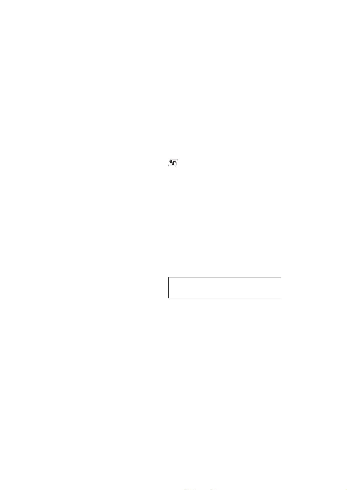
Index to Parts and
Controls
Refer to the pages indicated in
parentheses for details.
Front
1 i (headphone) jack* (21, 23, 34, 35,
84)
2 Built-in microphones (stereo/
directional) (21, 25, 26)
3 Operation indicator (21, 25, 27, 29, 53)
4 Display window (10, 11)
5 DIVIDE/
39)
6
7 z (record/pause) button (21, 25, 26,
27, 30)
x (stop) button (18, 22, 26, 28, 30, 34,
8
41, 43, 46, 47)
> (cue/fast forward) button (35)
9
J Nx (play/stop/enter) button
K . (review/fast backward) button
(35)
L VOL (volume) +/– button (23, 34)
M (repeat) A-B/
(34, 38, 46)
N ERASE button (43)
O Opning for a handstrap (A handstrap
is not supplied.)
(bookmark) button (31, 34,
(folder)/MENU button
(priority) button
* Connect stereo ear receiver or stereo
headphones supplied or not supplied to the
i (headphone) jack. If unwanted noise is
heard, wipe the headphones plug clean.
Rear
P Speaker
Q HOLD switch
R V-UP (Digital Voice Up) switch (37, 57)
S DPC switch (38, 51)
T DIRECTNL (directional) switch (24)
m (microphone) jack (31, 32)
U
V (USB) connector (13, 64)
W Battery compartment (13)
** Slide the HOLD switch in the direction of
the arrow to lock all the functions of all the
buttons. During stop, “POWER SAVING…”
will be displayed and the display will be
turned o to prevent battery power from
exhausting.
**
GB
9
3
Page 4
ICD-SX68/SX68DR9/SX78/SX78DR9/SX88
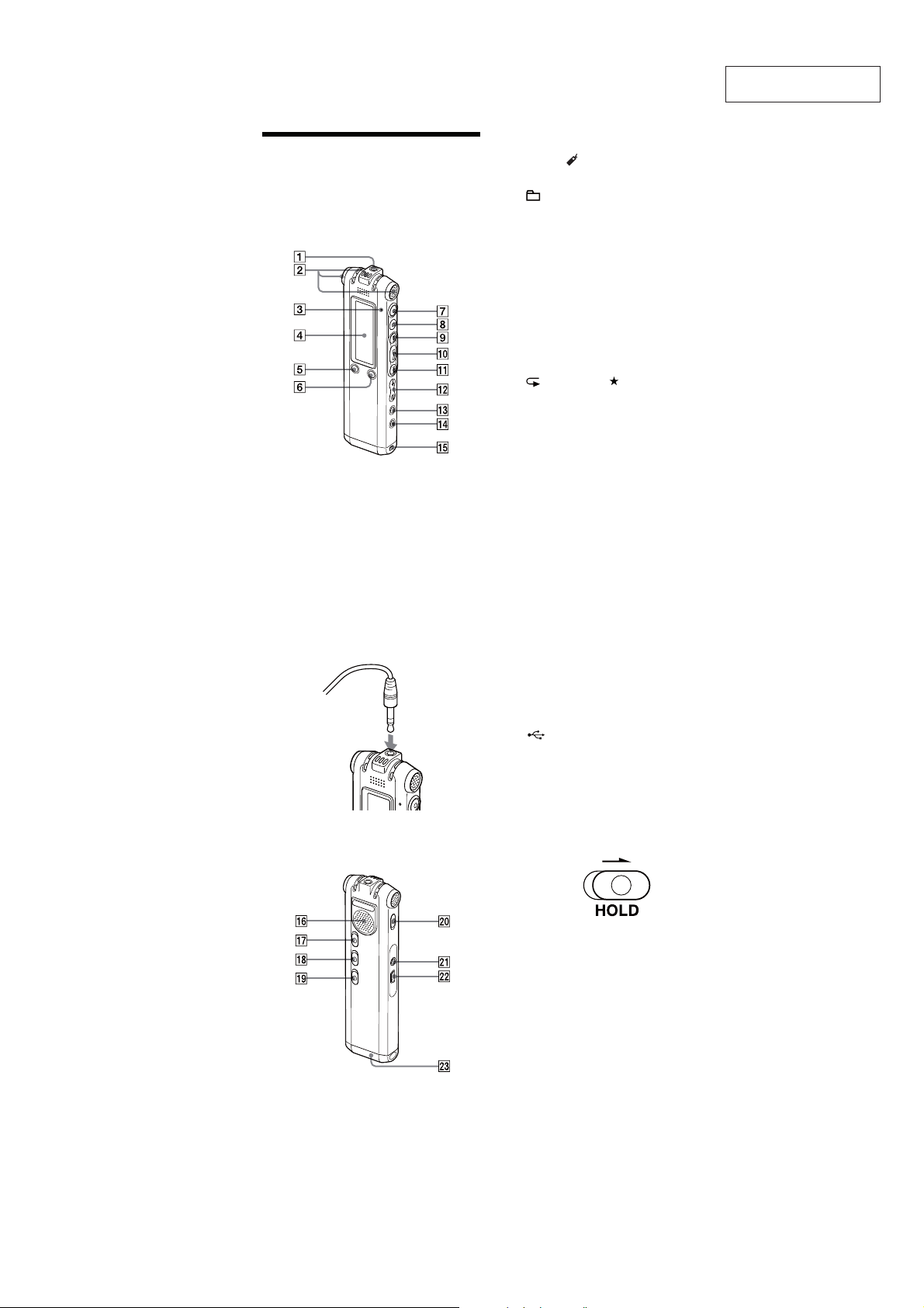
Display window
Display during playback and stop
1Operation mode indicator
Displays the following, depending on
the current operation mode
: playback
: stop
: review/fast backward,
cue/fast forward
: going backward/forward
continuously
2 Folder indicator
3 Elasped time/Remaining time
indication/Recording date and time
indication
4 Folder name/Message name/Artist
name indication
5 Remaining battery/Charging
indicator
When dry batteries are used, the
indicator shows the remaining
battery power.
While charging the rechargeable
batteries an animation appears.
6 Selected message number/Total
number of messages in the folder
7 Priority marks
Appear(s) when a message is set with
priority mark(s).
8 Bookmark indicator
Appears when a bookmark is set for
a message.
9 Alarm indicator
Appears when the alarm is set for a
message.
J
Displays the EFFECT setting in the
menu.
BA1 : The bass sound is reinforced.
BA2 : The bass sound is further
reinforced.
K Recording mode indicator
Displays the recording mode set
using the menu when the IC recorder
is in the stop mode, and displays the
current recording mode when the IC
recorder is in the playback mode.
STHQ : Standard play stereo
recording mode with high quality
sound
ST : Standard play stereo recording
mode
STLP : Long play stereo recording
mode
SP : Standard play monaural
recording mode
LP : Long play monaural recording
mode
MP3 : MP3 mode (during playback
only)
L Microphone sensitivity indicator
Displays the current microphone
sensitivity.
(high) : To record at a meeting or
in a quiet/spacious place.
(low) : To record for dictation or in
a noisy place.
MAN (manual) : To record with
microphone sensitivity set manually.
M Remaining recording time indication
Display during recording
N Operation mode indicator
Displays the following, depending
on the current operation of the IC
recorder.
: recording
: recording standby/recording
pause
: recording with the VOR
function
: recording pause with the
VOR function
O Recording level meter
P Microphone sensitivity indicator
Displays the current microphone
sensitivity when recording with AGC
(Automatic Gain Control).
(high) : To record at a meeting or
in a quiet/spacious place.
(low) : To record for dictation or in
a noisy place.
Displays the recording level during
manual recording.
Q Elapsed recording time indication
R Alarm indicator
S Recording mode indicator
Displays the recording mode (STHQ,
ST, STLP, SP, and LP) set in the menu.
T LIM (limiter) indicator
Displays the LIMITER setting in the
menu.
When “REC LEVEL” is set to “AUTOAGC,” “---” is displayed.
U Remaining recording time indication
V Remaining battery/Charging
indicator
W LCF (Low Cut Filter) indicator
Displays the LCF setting in the menu.
Step 2: Setting the
Clock
x
/>
.
Nx
/MENU
You need to set the clock to use the
alarm function or record the date and
time.
Clock setting display appears when you
you insert batteries after the IC recorder
has been without batteries for a certain
period of time. In this case, proceed from
step 4.
1 Select “DATE & TIME” in the menu.
1
Press and hold /MENU.
The menu mode will be displayed in
the display window.
2
Press . or > to select “DETAIL
MENU” and press
3
Press . or > to select “DATE &
TIME” and press
2 Press . or > to select “AUTO”
or “MANUAL” and press
When you selected “AUTO,” the clock is
automatically adjusted using the clock
in the computer connected to the IC
recorder and on which the supplied
Digital Voice Editor software is started.
When you select “MANUAL,” proceed
to the next steps.
3 Press . or > to select
“08y1m1d” and press
4 Press . or >to set the year,
month, day, hour, and minute in
sequence, and then press
“EXECUTING….” appears and the clock
is set.
5 Press x to return to the normal
display.
P
Note
If you do not press Nx within one minute
of entering the clock setting data, the clock
setting mode is cancelled and the window
will return to the normal display.
Nx.
Nx.
Nx.
Nx.
Nx.
4
Page 5
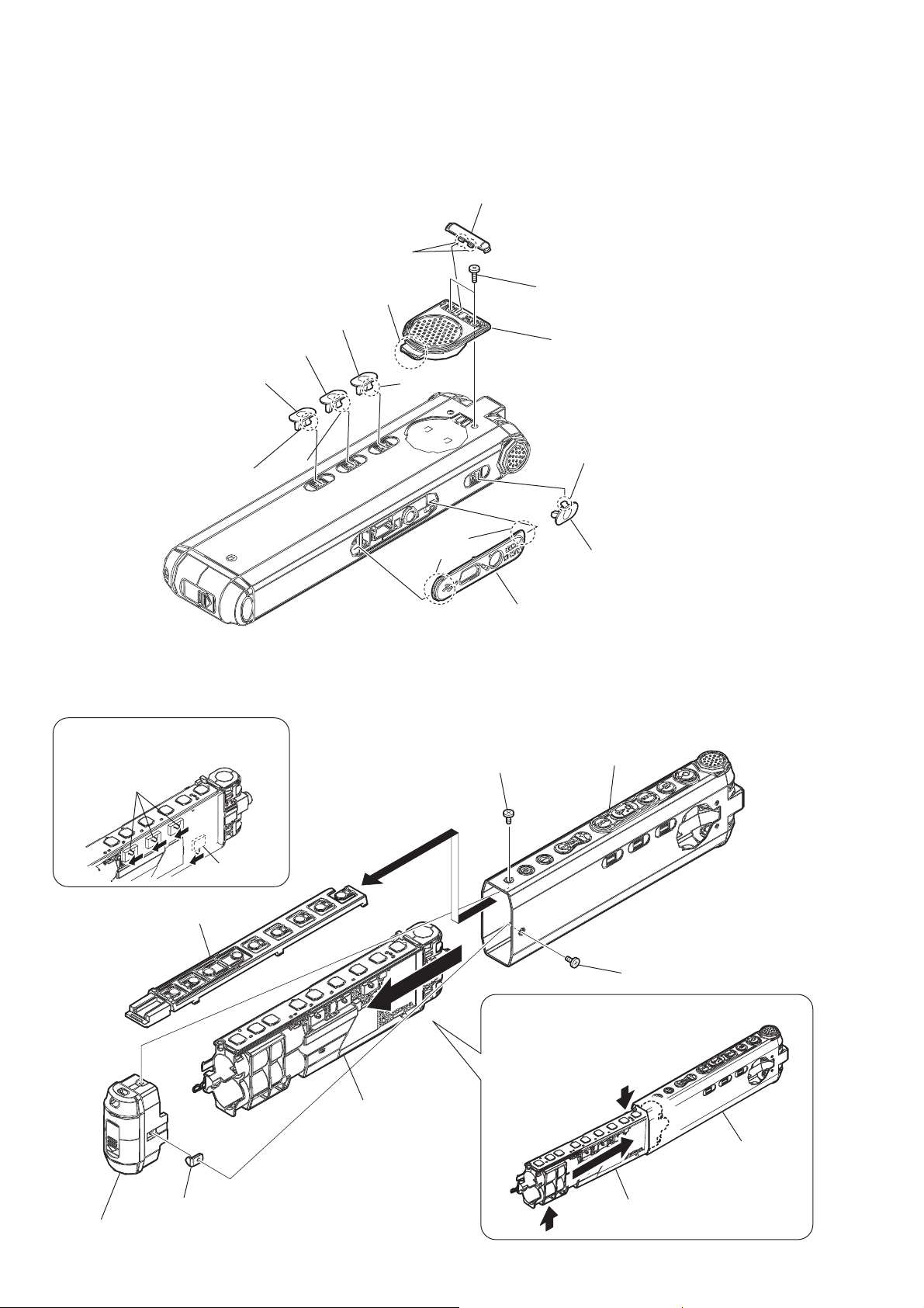
• This set can be disassembled in the order shown below.
SET
2-1.KNOB (HOLD),
SPEAKER ASSY (SP001)
(Page 6)
2-2.CHASSIS ASSY ,
CASE ASSY
(Page 6)
ICD-SX68/SX68DR9/SX78/SX78DR9/SX88
SECTION 2
DISASSEMBLY
2-4.COVER (CHASSIS),
MAIN BOARD
(Page 7)
2-5.CHASSIS
(Page 8)
2-6.SW BOARD,
HPJACK BOARD
(Page 8)
2-7.MIC-A ASSY,
MIC-B ASSY
(Page 9)
2-8.LIQUID CRYSTAL
DISPLAY PANEL,
AUDIO BOARD (Page 9)
2-3.BATTERY CASE LID
(Page 7)
5
Page 6
ICD-SX68/SX68DR9/SX78/SX78DR9/SX88
Note: Follow the disassembly procedure in the numerical order shown below.
2-1. KNOB (HOLD), SPEAKER ASSY (SP001)
RB two claws
RT base
knob (hold)
knob (hold)
claw
claw
2-2. CHASSIS ASSY, CASE ASSY
When assembling the chassis assy,
adjust the switches in the direction
of the arrow.
switches
RG claw
knob (hold)
claw
two
claws
RE two screws (1.7 × 4.5)
RH speaker assy (SP001)
R cover (jack)
screw (1.7 × 3.5)
claw
knob (hold)
case assy
switch
spacer (ornamental belt)
screw (1.4 × 2.5)
When assembling the chassis assy to the case assy,
orient the case assy so that its L side
faces down, and insert the chassis
assy with its left side up.
bracket (chassis)
battery case lid assy
chassis assy
left side
chassis assy
L side
faces
case assy
6
Page 7
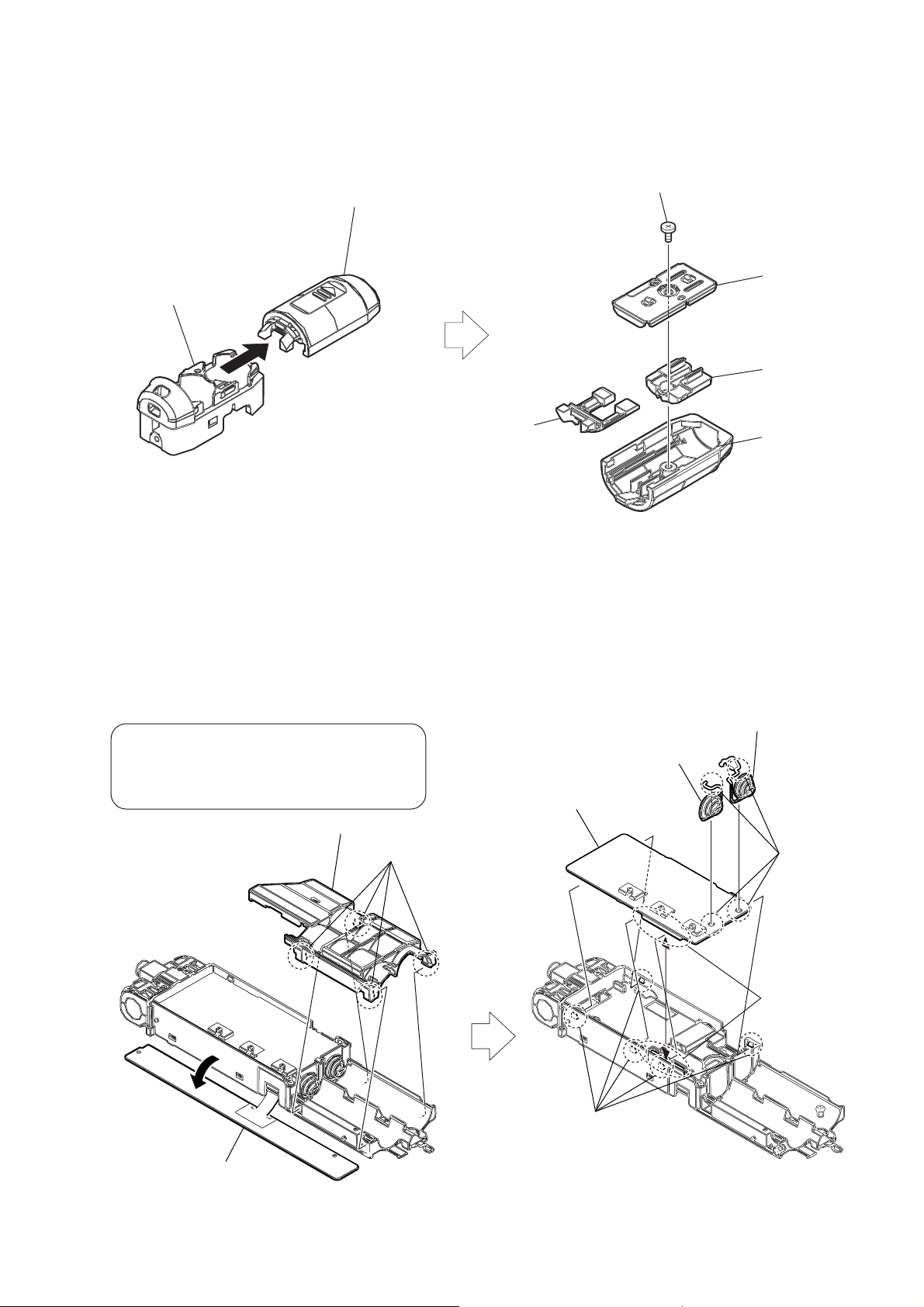
2-3. BATTERY CASE LID
chassis (battery case lid)
ICD-SX68/SX68DR9/SX78/SX78DR9/SX88
screw (1.7 × 3)
battery case lid,
base (battery), e.t.c.
battery terminal
(+–) assy
base (battery)
hinge
(battery case lid)
battery case lid
2-4. COVER (CHASSIS), MAIN BOARD
Assembling the chassis assy
After the chassis assy has been assembled,
check that the wires of the microphone are properly
routed (without being pressed down).
cover (chassis)
four claws
battery terminal (+)
battery terminal (–)
MAIN board
Remove the
solderings.
board to board
connector
five claws
Remove the SW board
in the direction of the arrow.
7
Page 8
ICD-SX68/SX68DR9/SX78/SX78DR9/SX88
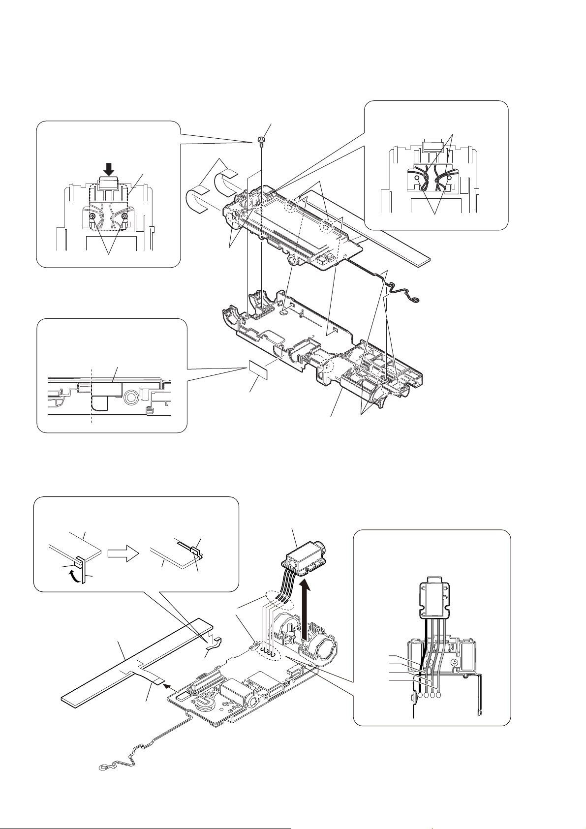
2-5. CHASSIS
When installing the HPJACK board,
push the board to the very end,
and then fix it with screws.
HPJACK board
screws
Sheet (microphone jack) attachment
position is shown.
sheet (microphone jack)
two cushions
two claws
sheet
(microphone jack)
two screws (B1.4 × 4)
two claws
chassis
Route the harness as shown below.
harnesses
screw holes
two claws and dowel.
2-6. SW BOARD, HPJACK BOARD
Sheet (LED) attachment position is shown.
SW board
LED
sheet (LED)
SW board
wire (frat type)
(CN7002)
SW board
Remove
the solderings.
sheet (LED)
sheet (LED)
LED
HPJACK board
Solder each lead according to the color
(black, orange, blue, gray) as shown in
the figure.
black
orange
blue
gray
8
Page 9
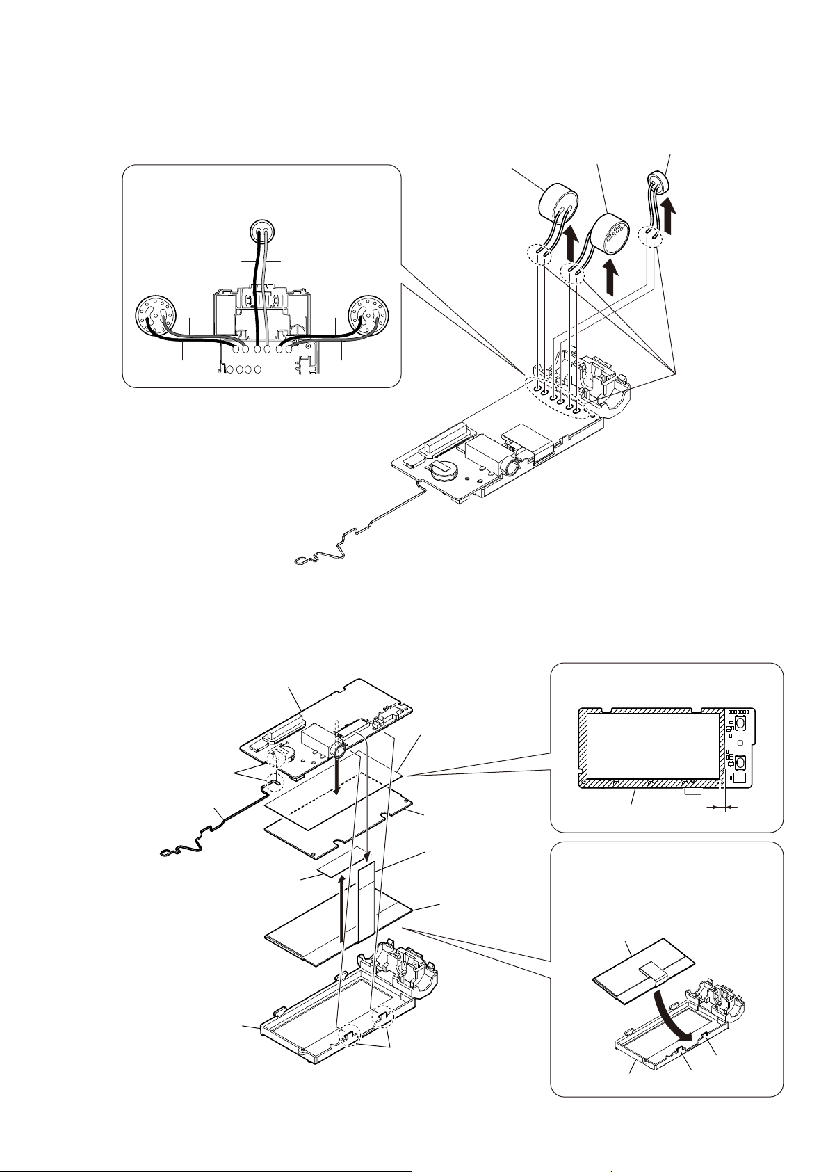
2-7. MIC-A ASSY, MIC-B ASSY
ICD-SX68/SX68DR9/SX78/SX78DR9/SX88
Solder each lead according to the color
(black, red, yellow) as shown in the figure.
mic-B assy
(M103)
black yellow
mic-A assy
(M101)
red
black
black
mic-A assy
(M102)
red
mic-A assy
(M101)
mic-A assy
(M102)
mic-B assy
(M103)
Remove the
solderings.
2-8. LIQUID CRYSTAL DISPLAY PANEL, AUDIO BOARD
R AUDIO board
sheet
(light guide plate L)
Remove the soldering.
battery terminal
(detection)
sheet (light guide plate S)
light guide plate
wire (frat type)
(CN5002)
liquid crystal
display panel
(LCD101)
Sheet (light guide plate L) attachment
position is shown.
Sheet
(light guide plate L)
AUDIO board
When installing the liquid crystal display
panel to the holder (LCD), insert the liquid
crystal display panel to the holder (LCD)
from the side with claws.
liquid crystal
display panel
1mm
holder (LCD)
two claws
holder (LCD)
claw
claw
9
Page 10
ICD-SX68/SX68DR9/SX78/SX78DR9/SX88
SECTION 3
TEST MODE
[Test Mode]
The following checks can be implemented using the Test Mode.
How to Enter the Test Mode
• Turn the power on. (by inserting batteries)
• Turn ON the [V-UP] switch while pressing the [DIVIDE/ ]
button and [VOL –] button at the same time.
How to Exit the Test Mode
Exit the test mode by turning OFF the power. (by removing the
batteries)
Initial Status of the Test Mode
When the machine enters the test mode, the LCD display appears
as shown below.
+
Loop
Select the desired item by using the [>]/[.] button, and
press the [Nx] button to set the selection.
START
TEST MODE
1. Version test
• Version of the respective modules are verifi ed.
F/W version of
Boot loader
ICX-XXX
Boot:X
ARM X.XX .XX / DSP X.X.XX
Oct XX 200X XX:XX:XX
F/W version of
CPU(ARM block)
• Press the [x] button to return to the test mode screen.
2. Key Chk + Format test
• Perform the key check by pressing the keys. The NAND formatting (deleting all events) and the default settings of the
menus (default language and LCD contrast remain unchanged)
are executed at the same time.
F/W version of
CPU(DSP block)
Total of 15 keys* are counted.
The checked key is display.
KeyChk+Fmt
Loop
ExtMic Cal
SetMic Cal
Beep
Lcd Cont
RTC Int
Battery
BattCnt
Initial status of test mode
F/W version display
Version
App LogOut
Log Output
Key Check
Convert
Menu Init
Sleep
VBUS
BattAB4
BattAC2
When all checks are
completed, the back-Light
turns on for 0.5 seconds
liant
* [
]/[>]/[.]/[ /MENU]/[z]/[x]/[VOL +]/
Nx
[VOL –] /[ERASE]/[DIVIDE/
The NAND formatting
(deleting all events)
and the befault settings
of the menus are completed.
]/[ A-B/ ]/
[DPC (ON/OFF)]/[V-UP (ON/OFF)]/
[DIRECTNT (ON/OFF)]/[. HOLD]
• Press the [x] button to return to the test mode screen.
10
Turn off the power
(Remove the batteries)
END
TEST MODE
Page 11
ICD-SX68/SX68DR9/SX78/SX78DR9/SX88
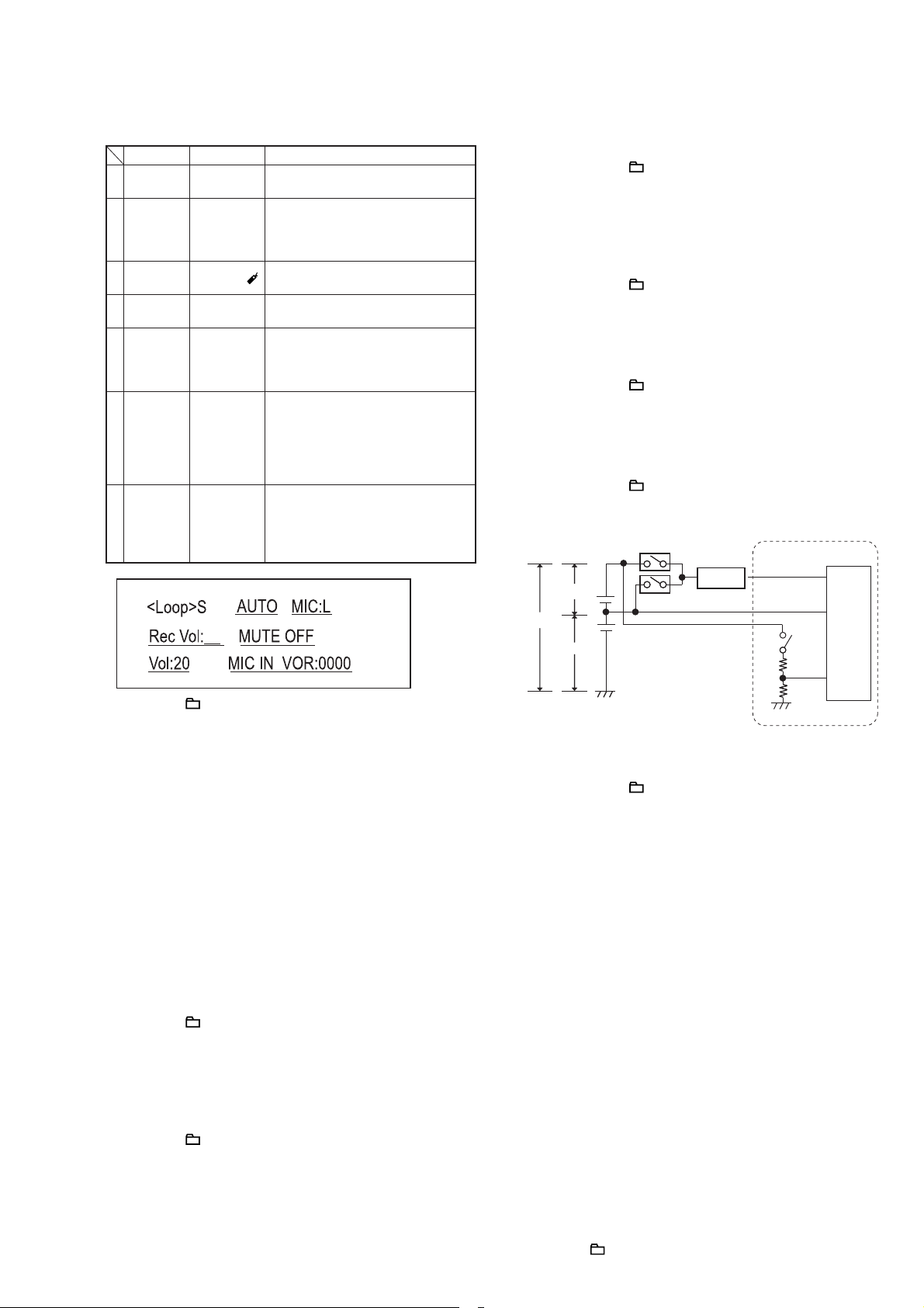
3. Loop test
Execute the DSP LOOP BACK.
Test
Sound vol-
1
ume test
Recording
2
level test
Muting test
Directivity [DIRECTNL]
6
Setting of
recording
3
AUTO/
MANUAL
Sensitivity
4
/ Limitter
Selection
of the
external
5
microphone
Key SWITCH
[VOL +],
[VOL –]
[.], [>]
[DIVIDE /
[.HOLD]
[V-UP]
[DPC]
]
Description
The sound volume can be adjusted
(Default value is 20.)
Press the [.HOLD] switch to ON
for MANUAL mode.
The recording level can be adjusted
(Default value is 30.)
Muting test can be set to “ON” or
“OFF”.
“ON” or “OFF” of the switch can be
set the directivity of the microphone.
OFF: AUTO
ON: MANUAL
AUTO ([.HOLD] SW:ON):
(OFF: Sensitivity H, ON: Sensitivity L)
MANUAL ([.HOLD] SW:ON):
(OFF: Limitter OFF, ON: Limitter
ON)
Press the [.HOLD] switch to ON
for MANUAL mode.
OFF: MIC IN, ON: AUDIO IN
• Press the [ /MENU] button to return to the test mode
screen.
4. ExtMic Cal
• The external microphone R and L channels level difference is
calibrated.
• Press the [Nx] button to start calibration.
• Press the [x] button to return to the test mode screen.
5. SetMic Cal
• The internal microphone R and L channels level difference is
calibrated.
• Press the [Nx] button to start calibration.
• Press the [x] button to return to the test mode screen.
6. Beep test
• Beep sound of 1.3 kHz is output.
• Press the [Nx] button to start outputting and press the [x]
button to stop.
• Press the [
/MENU] button to return to the test mode
screen.
9. Battery test
• The detected A/D value of the battery remaining power is
checked.
• Press the [x] or [ /MENU] button to return to the test mode
screen.
10. Batt Cnt test
• The present A/D value of the center of the battery remaining is
checked.
• When the battery is not connected, NG is display.
• Press the [x] or [ /MENU] button to return to the test mode
screen.
11. Batt AC2 test
• The present A/D value of the side of VBatAC x2 on the error
amplifi ed circuit (IC1603 output) is checked.
• Press the [x] or [ /MENU] button to return to the test mode
screen.
12. Batt AB4 test
• The present A/D value of the side of VBatAB x4 on the error
amplifi ed circuit (IC1603 output) is checked.
• Press the [
] or [ /MENU] button to return to the test mode
x
screen.
* : 11, 12 items, refer to following fi g.
VBatAC
VBatBC
VBatAB
Q1664
Q1663
x2SIDE
x4SIDE
IC1603
ErrorAmp
C
B
A
70k
110k
IC1001
ADIN7
(VBAT_ERR)
ADIN8
(VBAT_CNT)
ADIN1
(VCCVBAT)
13. VBUS test
• The present value of the VBUS is checked.
If it is connected, OK is display.
• Press the [
] or [ /MENU] button to return to the test mode
x
screen.
14. Sleep test
• Sleep is tested.
Note: When <Sleep> is selected, the machine enter the sleep mode. To
exit the sleep mode, turn off the power, by removing the batteries
and reenter the test mode.
15. Menu lnit
• Press the [Nx] button to enter the menu initialization.
• Press the [
] button to return the test mode screen.
x
16. Key Chk test
• Key check only is executed when the key is pressed.
• Press the [
] button to return to the test mode screen.
x
7. LCD Cont test
• Adjust the LCD contrast.
Default value is 10.
• Adjust the LCD contrast using the [>]/[.] button.
• Press the [
/MENU] button to return to the test mode
screen.
8. RTC Interrupt test
• Perform the self test of the RTC.
• Press the [x] button to return to the test mode screen.
17. Log Output test
• This is the log output to be used for engineering design.
Note: Not used.
• Press the [x] button to return to the test mode screen.
18. App Log Out test
• This is the app log out to be used for engineering design.
• Press the [x] button to return the test mode screen.
19. Convert test
• This is the conversion out to be used for engineering design.
• Press the [ /MENU] button to exit the test mode.
11
Page 12

ICD-SX68/SX68DR9/SX78/SX78DR9/SX88
SECTION 4
DIAGRAMS
THIS NOTE IS COMMON FOR PRINTED WIRING BOARDS AND SCHEMATIC DIAGRAMS.
(In addition to this, the necessary note is printed in each block.)
For Printed Wiring Boards.
Note:
• X : Parts extracted from the component side.
• : Pattern from the side which enables seeing.
(The other layers' patterns are not indicated.)
Caution:
Parts face side:
(SIDE A)
Pattern face side:
(SIDE B)
• Lead layouts
Parts on the parts face side seen from
the pattern face are indicated.
Parts on the pattern face side seen from
the parts face are indicated.
CSP (Chip Size Package) Lead layout of conventional IC
surface
For Schematic Diagrams.
Note:
• All capacitors are in μF unless otherwise noted. (p: pF)
50 WV or less are not indicated except for electrolytics
and tantalums.
• All resistors are in Ω and
specifi ed.
• f : internal component.
• C : panel designation.
• A : B+ Line.
• Power voltage is dc 1.5V and fed with regulated dc power
supply from battery terminal.
• Voltages are dc with respect to ground under no-signal
(detuned) conditions.
no mark : REC
( ) : PLAY
* : Impossible to measure
• Voltages are taken with a VOM (Input impedance 10
MΩ).
Voltage variations may be noted due to normal production
tolerances.
• Signal path.
F : PB
L : REC
1
/4 W or less unless otherwise
12
Page 13
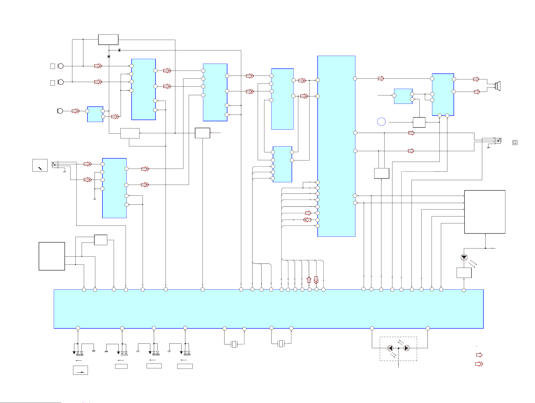
ICD-SX68/SX68DR9/SX78/SX78DR9/SX88
ICD-SX68/SX68DR9/SX78/SX78DR9/SX88
1313
4-1. BLOCK DIAGRAM - MAIN1 SECTION -
Signal path
: REC
: PB
27
9
CS
SDA
IC3404
REG
IC1001(1/2)
SYSTEM CONTROLLER
OUTP
OUTN
Q3304
MUTE
Q5001
LED DRIVE
D5005,5004,5002
Q3402
SWITCH
J3301
(SPEAKER)
13
14
11
2
3
IC3654
VOLUME CONTROL
WA
WB
SCLK
DIN
4
CS
LA
10
LB
3
7
10
5
8
IC3203
SELECTOR
IN2
COM1
COM2
2
NO1
D3607
D3606
IN1
9
4
NC1
NO2
NC2
3
7
8
5
10
IC3655
SELECTOR
IN2
VDD_HP
COM1
COM2
4
NO1
IN1
9
2
NC1
NO2
NC2
SCK
IC3901
ADC, DAC, HEADPHONEAMP
AIN1L
30
31
MD/ADA
AS/ADR
MC/SCR
LRCK
PCM0_LRCK
BCK
PCM0_BCK
DIN
DOUT
SCKI
HPCOM/MONO
HPOL/LOR
HPOR/LOR
17
16
V10
KS-1IPS
W8
OS-1IPS
W10
OZSC-1IPS
OMWP
AC22
AD22
AB22
AC21
KLC-OMP
NES-OMP
IS-OMP
OS-OMP
U18
OKLCFER
2ZSC-OIPS
SPI1_CLK
SPI1_MOSI
AGC_XCS
KLC_1IPS
ISOM_1IPS
SCX_CGA
IDT-D
KCT-D
V17
SMT_D
NWDP
NETUM
U19
AC6
AB2
W22
AA2
0ZSC-0IPS
KS-OIPS
OS-OIPS
Y3
80IPG
AA1
AC7
AC8
AC23
AD7
110IPG
010IPG
210IPG
SP001
+
-
FUNCTION
SWITCH
R
(MIC CENTER)
IC3403
POWERAMP
IC3904
MICAMP
IN+
OUT
V+
1
5
4
J3201
PLUG IN
POWER
S6014
S6015
HOLD
23
AIN3R
AIN3L
22
29
32
22W-0A-DLCB
91U-TSRX-DLCB
6CA-SC-DLCB
2BA-TEDX-JPH
1AA-ETUM-PS
2AA-RWP-PS
3Y-ETUM-PH
7CA-KLC-OIPS
8CA-ISOM-OIPS
PWM
ADA_XCS
1
2
PCM0_DADT
3
PCM0_ADDT
7
CPU_RFFCLK0
KCRL_0MCP
KCB_0MCP
MWP
SCX_ADA
TDAD_0MCP
TDDA_0MCP
0KLCFFR_UPC
4
5
15
2
IN
VDD2
UNREG35-DET
MAIN2
SECTION
(Page 14)
VDD1
VOUT
VIN
+3.3V
CE
L
1
5
6
IC3202
AMP
A OUTPUT
B OUTPUT
3
A+INPUT
A-INPUT
B+INPUT
B-INPUT
7
2
3
7
10
5
8
IC3024
SELECTOR
COM1
COM2
2
NO1
IN1
IN2
9
4
NC1
NO2
NC2
VDD_GP2
VDD_GP2
Q3660
SWITCH
Q3657
SWITCH
Q3659
SWITCH
TEDX_CIMTXE
1LES_CIM
2LES_CIM
RWPX_CIM
LES_ENILX_CIM
1DA_YEK
0DA_YEK
EKAW-YEK
B6
4NIDA
AD4
10IPG
AD3
20IPG
C6
3NIDA
IS_1MP
OS_1MP
Q6001
SWITCH
AD5
AA3
AD20
AC20
NES_1MP
AB20
KLC_1MP
AB21
0OIPG
9OIPG
CD
RES
LIQUID
CRYSTAL
DISPLAY
26
AIN1R
12
10
14
16
1
3
OFF
ON
V-UP
OFF
ON
S6016
AD2
30IPG
DPC
OFF
ON
S6013
AC5
40IPG
T26
OKC
U26
IKC
DIRECTNL
OFF
ON
X1401
11.2896MHz
AC26
NICSO
AB26
TUOCSO
X1601
32.768KHz
W3
510IPG
GRNK
D5004
REDK
W2
410IPG
A
S6001,S6002,S6004
S6005-6008
S6010,S6012,
S6509,S6511
(MIC)
(MIC)
M101
M102
M103
LCD101
Page 14
ICD-SX68/SX68DR9/SX78/SX78DR9/SX88
ICD-SX68/SX68DR9/SX78/SX78DR9/SX88
1414
4-2. BLOCK DIAGRAM - MAIN2 SECTION -
Signal path
: REC
: PB
H4-8
G5-8
E5-7
F5-8
H22-25,F25
C25,G23-25
E25,J22-24
F24,D24,25
H2,3
G3,4
F4,E4
H18,19
D18,20
C20,E18
AB0_A25/DPQ
AB0_F24/DAK
A2,A8,B1
B2,B8,B9
C1,C2,C8
C9,D1,D2
D8,D9,E1
E9
H9-7,
H3-1,
G3,G2,
J8,7,
J3,2
U2-5,
V8,4,5
W4,5,
Y4,5,
AA4
R1,R8,N1,
N2,N3,N4,
N5N8,M4,
M5,M8,P1,
P2,P3P4,
P8,
GPI07
Q8501
SWITCH
J5
SDR_DATA30
G4
EXTRST
DQ0-7
DQ8-12
DQ13-15
F1R4
DQM1
E8
LDQM
SDR_DQM1
SDR_DQM0
SDR_DATA0-15
SDR_A0-11
P5
IC2602
SRAM
IC1001(2/2)
SYSTEM CONTOLLER
A4
NAND_WEZ
IC2701
FLASH
MEMORY
I/01-I/08
NAND_DA0-DA7
E1
E2
XIN
C2
VBUS
B1
DM
C1
1
1
4
4
DP
XOUT
X8501
24MHz
C4
A6
A0-A11
DREQO_N
D4
DACK0-N
A5
CS_N
C5
WR0_N
RST_N
SDR_DATA31
C6
4
3
1
4
2
1
4
4
INT_N
B5
WR1_N
RD_N
AB0_A1 -A6
AB0_D00 - D15
AB0_A1-A6
AB0_D0 - D15
1
2
5
VBUS
D-
GND
ID
3D+
4
IC8503
USB CONTROLLER
CN8002
(USB)
VBUS
F8
SDR_WEZ
SDR_RASZ
SDR_CASZ
SDR_CKE0
SDR_CLK
SDR_BA0
T5
F7
U8
F3
CKE
T1
F2
CLK
AA5
EXM_RDZ
J19
AB0_WRZ
H16
E3
NAND_REZ
H13
NAND_DA15
E9
NAND_CLE
NAND_XWE
NAND_XRE
NAND_XWP
NAND_CLE
NAND_ALE
NAND_XCS0
NAND_XCS1
NAND_RXBO
NAND_RBZO
D3
NAND_ALE
M9
NAND_CSZ0
NAND_CSZ1
C2
D2
NAND_RXB1
NAND_RBZ1
H8
19
XWP
18
XWE
17
ALE
16
CLE
10
XCE2
9
XCE1
8
XRE
7
R/B1
H26
PDAGHC
H17
E24
F23
AB3
A2
AB0_CSZ0
E11
TABWS_WSP
CS
G9
SDR_CSZ0
T3
BA1
G8
SDR_BA1
T4
G7
BA0
AB5
F9
R5
NAND_XWE
NAND_XRE
NAND_XWP
NAND_CLE
NAND_ALE
NAND_XCS0
NAND_XCS1
NAND_RXBO
6
R/B2
NAND_RXB1
29-32
41-44
B4,C4,D4
E4,L9,E6,
K9,E8
WE
RAS
CAS
H5
Q1665
SWITCH
Q1667
SWITCH
Q8004
SWITCH
IC8504
DETECT
Q8502
SWITCH
D1601
IC1802
DC/DC CONV.
VDD_DCCOUT33
VDD_UNREG
+3.1V
IC8501
+3.1V REG
UNREG35-DET
MAIN1
SECTION
(Page 13)
VOUT
SHDN
4
1
DRY BATTERY
SIZE "AAA"
(IEC DESIGNATION LR03)
2PCS. 3V
SWITCH
Q1608
Q1664
SW
SW
Q1663
IC8003
DETECT
Q1609
SWITCH
+1.5V
IC1603
AMP
INT+
OUT
IC8001
DETECT
VOUT
VIN
IC8502
+1.5VREG
IC8002
RESET
SWITCH
Q1668
A17
SUBV
E15
SUBVWS_WSP
K26
GHC
D15
2SUB-WS_WSP
G22
3ZSC-0BA
2ZSC-0BA
F22
C8
7NIDA
SWITCH
Q1603
A
SWITCH
Q1601
Page 15

ICD-SX68/SX68DR9/SX78/SX78DR9/SX88
ICD-SX68/SX68DR9/SX78/SX78DR9/SX88
1515
4-3. PRINTED WIRING BOARD - AUDIO BOARD (SIDE A) -
Ref. No. Location
• Semiconductor
Location
D5002 B-6
D5004 B-5
D5005 B-4
Q3657 B-2
• : Uses unleaded solder.
Q3657
2 1 3
B
C3688
D5002
D5005
C6001
R3302
C1004
C3913
R6001
R6003
C3999
R3319
R6008
31
4
S
2
S6001
S6001
31
42
S6004
S6004
R6034
R3318
R6035
R6036
R6037
R6038
C6032
R3738
D5004
D5002,5004,5005
(LCD BACK LIGHT)
JL6110
+
AUDIO BOARD (SIDE A)
DIVIDE /
/ MENU
1-872-141-
12
(12)
23456781
A
B
C
D
Page 16

ICD-SX68/SX68DR9/SX78/SX78DR9/SX88
ICD-SX68/SX68DR9/SX78/SX78DR9/SX88
1616
4-4. PRINTED WIRING BOARD - AUDIO BOARD (SIDE B) -
• : Uses unleaded solder.
234567
8
1
A
B
C
D
IC3654
IC3655
IC3904
IC3901
IC3202
IC3203
IC3024
13
(13)
C
SW BOARD
(Page 26)
B
MAIN BOARD
CN1001
(Page 19)
A
HPJACK
BOARD
(Page 26)
RED
R
M102
M103
M101
(MIC)
CENTER
MIC
BLACK
YELLOW
BLUE
ORANGE
BLACK
RED
BLACK
GRAY
BLACK
AUDIO BOARD (SIDE B)
L
(MIC)
( )
+
P
+
P
+
P
+
P
+
P
A
+
A
+
113
*
1-872-141-
7033R
R6019
3306R
1023R
JL3201
F
FB3302
FB3303
JL3408
9043LJ
0143LJ
2233R
R3324
R3323
9863C
7093R
R3908
1033B
3023R
5023R
3963C
JL3205
7043LJ
93C
R3910
C3324
5233R
1
2
3
45
CSP
(Chip Size Package)
5
610
1
11
JL3203
JL3204
JL3206
1193R
Q3660
6063D
D3607
9093C
S
2 1 3
C3904
2093R
R3905
JL3202
80
R3913
4193R
Q3659
2863C
1963C
4005C
5005C
Q5001
C5011
R5013
R5023
R3714
R3909
C3907
S
S
3 1 2
LCD101
LIQUID CRYSTAL DISPLAY
DIRECTNL
S6013
ON OFF
CSP
(Chip Size Package)
CSP
(Chip Size Package)
C3665
C3690
1
4
5
8
912
13
16
17
5
610
1
11
C3692
C3696
C3697
C3308
3
R3315
5073R
R3706
R3719
R3720
1373R
2123C
C3215
C3216
58
4
1
6133R
R3320
R3321
*
*
(Chip Size Package)
C3307
4033Q
033R
4033R
C3914
C3915
C3916
C3917
4133R
8
1
427
1
5
2
6
1
239
3
3
C1002
*
C5001
C5002
C5003
R5008
2105R
FB3201
3023BF
0123C
2023
R
R3207
0
10
6
206
CN5002
4105R
21
93R
C3683
6863
C
7863C
2023B
F
C1003
307
3R
C3217
C3218
R3204
123R
1123R
3D
R3215
3D
30
63D
4063D
0193C
CSP
(Chip Size Package)
7073R
2306R
C3211
90
23R
R3213
5063D
5
601
1
11
C3911
C6033
*
BT1602
LITHIUM
SECONDARY
BATTERY
3V
CSP
C1001
50
491
2
CN7001
1
CN7002
J3201
8
Ref. No. Location
• Semiconductor
Location
D3601 B-4
D3602 B-4
D3603 C-4
D3604 C-4
D3605 C-3
D3606 D-7
D3607 D-7
IC3024 C-3
IC3202 C-5
IC3203 B-6
IC3654 C-5
IC3655 C-6
IC3901 C-4
IC3904 B-7
Q3304 D-5
Q3659 B-6
Q3660 D-7
Q5001 B-6
Page 17

ICD-SX68/SX68DR9/SX78/SX78DR9/SX88
ICD-SX68/SX68DR9/SX78/SX78DR9/SX88
1717
4-5. SCHEMATIC DIAGRAM - AUDIO BOARD (1/2) -
AUDIO
BOARD
( 2 / 2 )
(Page 18)
101
AUDIO
BOARD
( 2 / 2 )
(Page 18)
102
IC3203
SELECTOR
IC3655
SELECTOR
IC3202
AMP
IC3654
VOLUME CONTROL
IC3024
SELECTOR
IC3904
MICAMP
L
R
18 19 20
2.9(0)
2.8(0)
2.8
0
2.8(0)
2.8(0)
0
2.8(0)
2.8(0)
2.9(0)
2.9(0)
2.8(0)
2.9(0)
2.9(0)
2(0)
0
2.9(0)
0
2.8(0)
2.9(0)
0
0
0
0
0
0
0
0
0
)0(9.2
0
0
0
0
0
2.9(0)
2.9
2.8(0)
0
0
0
000
0002.9(0)
2.9(0)
0
0
0
0
0
0
0
0
No mark : REC
( ) : PLAY
JL3201
JL3202
4.7k
R3201
JL3203
JL3204
4.7k
R3203
1M
R3207
C3210
0.1
EXTMIC_XDET_AA3
R3215 4.7k
VDD_HP
J3201
1
2
3
4
4.7k
R3205
JL3205
JL3206
VDD_ANA
AGND
FB3203
FB3202
FB3201
MICIN_L
MICIN_R
k74
6073R
0.1
C3665
NJM2732RB1(TE2)
IC3202
12
34
5678
47k
R3719
470
R3714
k74
5073R
k740273R
MIC_SEL1
MIC_SEL2
0.1
C3682
0.1
C3683
k224023R
22k
R3209
0.1
C3212
1k
R3210
1k
R3211
0.47
C3217
0.1
C3999
0.47
C3218
3LP01S-K-TL-E
Q3657
S
MIC_XPWR
0.1
C3211
MIC_XLINE_SEL
16-ET004SS1
1063D
1
2
16-ET004SS1
2063D
1
2
16-ET004SS1
3063D
1
2
16-ET004SS1
4063D
1
2
AGC_XCS_W10
0.22
C3215
0.22
C3216
0.47
C3686
0.47
C3687
6.3V
10
C3689
0.1
C3690
SPI1_MOSI_W8
SPI1_CLK_VI0
6.3V
4.7
C3691
4.7
C3692
6.3V
470
R3731
10
R3738
100p
C3696
100p
C3697
3LP01S-K-TL-E
Q3659
6.3V
100
C3688
1SS400TE-61
D3605
k1
7073R
k1
3073R
C3904
0.1
123
45
R3902
100k
R3905
10k
R3907
47k
R3908
47k
NJM2741F3(TE1)
IC3904
4.7k
R3909
1
C3907
0.47
C3908
3LP01S-K-TL-E
Q3660
220
R3910
1SS400TE-61
D3606
1SS400TE-61
D3607
1M
R3911
MAX5488ETE
IC3654
1234
5678
9101112
3141516171
MAX4762ETB
IC3655
12345
678901
11
MAX4762ETB
IC3203
12345
678901
11
MAX4762ETB
IC3024
12345
678901
11
100p
C3909
0.47
C3693
0
R3912
10k
R3913
10k
R3914
1
C3910
1
C3911
220k
R3202
AGC_XCS_W10
MIC_C
MIC_L
MIC_R
VDD_STMIC
VDD_MICAMP
EXTMIC_R-1
EXTMIC_L-1
EXTMIC_XDET-2
VCC
NO1
COM1
NC1
IN1
NO2
COM2
NC2
IN2
GND
A OUTPU T
A-INPUT
A+INPUT
GND
B-INPUT
B OUTPUT
B+INPUT
V+
VCC
NO1
COM1
NC1
IN1
NO2
COM2
NC2
IN2
GND
VCC
NO1
COM1
NC1
IN1
NO2
COM2
NC2
IN2
GND
N.C.
GND
WA
HA
LA
N.C.
N.C.
N.C.
.C.N
BL
BW
BHDDV
KLCS
NID
SC
(0)
(1)
(0)
(1)
(1)
(0)
(1)
(0)
(1)
(0)
(1)
(0)
V+
OUT
IN-
GND
IN+
(CENTER)
SWITCH
SWITCH
SWITCH
*
*
*
*
CSP
(Chip Size Package)
CSP
(Chip Size Package)
CSP
(Chip Size Package)
CSP
(Chip Size Package)
AUDIO BOARD (1/2)
(MIC)
M101
M102
M103
(MIC)
(MIC)
*
*
S
S
R3213
4.7k
Page 18

ICD-SX68/SX68DR9/SX78/SX78DR9/SX88
ICD-SX68/SX68DR9/SX78/SX78DR9/SX88
1818
4-6. SCHEMATIC DIAGRAM - AUDIO BOARD (2/2) -
• See page 28 for IC Block Diagram.
SW
BOARD
(Page 27)
C
HPJACK
BOARD
(Page 27)
A
MAIN
BOARD
CN1001
(Page 21)
B
AUDIO
BOARD
( 1 / 2 )
(Page 17)
102
AUDIO
BOARD
( 1 / 2 )
(Page 17)
101
7
8
2
4
56
3
1
SS
2.8
0
0
3
3
0
No mark : REC
IC3901
ADC, DAC, HEADPHONEAMP
18 19
M
DIRECTNL
MICIN_L
MICIN_R
VDD_HP
JL3408
4.7
R3303
FB3302
2.2
R3314
JL3409
JL3410
FB3303
4.7
R3304
0.22
C3307
0.22
C3308
470k
R3307
JL3407
2.2
R3315
FB3301
NTHD4508NT1G
MUTE
Q3304
0.1
C3913
470k
R3302
0.1
C1001
0.1
C1003
4V
100
C3914
4V
100
C3915
100k
R3319
10k
R3318
0
R3316
0.1
C3916
0.1
C3917
0.001
C1004
47
R3320
47R3321
PCM3794RHBR
CSP
(Chip Size Package)
IC3901
12345678
901112131415161
1718192021222324
526272829203132333
0R3322
C3324
0.1
1k
R3323
1k
R3324
1
C1002
220k
R3325
HP_R_TP
HP_L_TP
HP_XDET_TP
HP_AGND_TP
R2NIA
L3NIA
R3NIA
BCIM
CCV
DNGA
MOCV
LOL/LOPH
AIN2L
AIN1R
AIN1L
MODE
MS/ADR
MD/ADA
MC/SCL
LRCK
HPOR/LOR
SPOLP
SPOLN
PGND
VPA
SPORP
SPORN
HPCOM/MONO
KCB
NID
TUOD
OIV
DDV
DNGD
IKCS
ITDH
MIC_SEL1
MIC_SEL2
MIC_XLINE_SEL
VDD_ANA
AGC_XCS_W10
EXTMIC_XDET_AA3
MIC_XPWR
SPI1_MOSI_W8
SPI1_CLK_VIO
FMGND
AGND
AGND
AGND
MIC_SEL1
MIC_SEL2
MIC_XLINE_SEL
VDD_HP
AGC_XCS_W10
EXTMIC_XDET_AA3
MIC_XPWR
CPU_REFCLKO
VDD_LOG
VDD_ANA
BATT_CNT_B8
PCM0_DADT_AC22
SPI1_MOSI_W8
PWM_0_AC23
PCM0_LRCK_AB22
ADA_XCS_AD7
PCM0_BCK_AC21
PCM0_ADDT_AD22
SPI1_CLK_V10
MONO_OUT
VDD_PUP_Y2
HP_MUTE_Y3
HP_XDET_AB2
TU_XCS_F23
FM_PWR
SPI1_MISO_AB8
CPU_CKI32
SPI0_MOSI_AC8
VDD_DDCOUT33
SPI0_CLK_AC7
BLCD_A0_W22
BLCD_CS_AC6
VDD_GP2
BLCD_LIGHT_V17
BLCD_XRST_U19
KEY_AD0_C6
OPLED_XGRN_W3
KEY_AD1_B6
OPLED_XRED_W2
KEY_WAKE-CN
KEY_XDICT_AC5
RTC_BKBAT_AD17
SGND
DGND
DGND
DGND
50P
CN7001
1
2
3
4
5
6
7
8
9
10
11
12
13
14
15
16
17
18
19
20
21
22
23
24
25
26
27
28
29
30
31
32
33
34
35
36
37
38
39
40
41
42
43
44
45
46
47
48
49
50
1k
R6003
10k
R6001
1k
R6008
C6001
0.1
470k
R6019
S6013
2
MOC
1KM3
RB
4S1
5
S2
6
S3
7
S4
S6004
1
1A
2
2A
3
1B
4
2B
S6001
11A2
2A
3
1B
4
2B
BT1602
LITHIUM
SECONDARY
BATTERY
3V
4.7k
R6032
0
R6033
R6035
10k
C6032
0.1
2200
R6034
470R6037
OPLED_XGRN
OPLED_XRED
VDD_GP2
SGND
KEY_AD0
DGND
KEY_AD1-3
KEY_WAKE
2.2kR6036
1kR6038
8P
CN7002
1
2
3
4
5
6
7
8
0.1
C6033
BKBAT+
BKBAT-
DIVIDE/BM MENU/FOLDER
R5012
100
100
R5013
1M
R5023
0.1
C5011
4.7
C5005
0.1
C5001
0.1
C5003
0.1
C5002
4.7
6.3V
6.3V
C5004
RTF025N03TL
LED DRIVER
Q5001
S
10M
R5008
13P
CN5002
1
2
3
4
5
6
7
8
9
10
11
12
13
100
R5014
SML-A12MT
D5005
SML-A12MT
D5002
D5002,5004.5005
(LCD BACK LIGHT)
SML-A12MT
D5004
CS
RES
CD
SCK
SDA
VDD
VSS
VBIAS
VLCD
VB0+
VB0-
VB1+
VB1-
JL6110
AUDIO BOARD (2/2)
*
*
LCD101
LIQUID
CRYSTAL
DISPLAY
IC B/D
DIVIDE
MENU
(1/5)
Page 19

ICD-SX68/SX68DR9/SX78/SX78DR9/SX88
ICD-SX68/SX68DR9/SX78/SX78DR9/SX88
1919
4-7. PRINTED WIRING BOARD - MAIN BOARD (SIDE A) -
• : Uses unleaded solder.
23456781
A
B
C
D
14
(14)
1041X
1061
X
L1601
2061L
1072R
1058C
20
5
8C
C8503
C8504
5058C
1
2
3
1058
Q
6058C
C8509
C8511
C8512
C8513
C8514
49
50
2
1
CN1001
7058R
8058R
R8509
1
34
5
21
34
5
2
R8510
1
1
5
8R
R8512
R8513
R8514
R8515
C1404
C1405
C1408
11
4
1C
C1608
C1605
R6026
9061C
C1416
8141C
C1419
C1803
C1805
2161C
31
6
1C
4161C
C1421
6161C
2241C
C1617
4241C
C1425
C1426
R1401
C1429
0261C
R1404
R1406
7041R
C1430
9041R
C1432
C1627
C1434
8261C
7341C
C1438
0
3
61C
C1631
3361C
1
54
3
4361C
C1441
53
6
1C
C1637
1161R
9
3
61C
C1445
C1446
7441C
1461C
2061HT
C1643
R1815
R1816
2
561C
+
P
2062C
3062C
3661C
4062C
C2605
C2606
Q1663
C2608
Q1664
Q1665
R1641
R1642
1
2
3
7
661
Q
R1645
51
CN8002
1072BF
5062R
R1666
R1667
Q8004
8
6
6
1R
9661R
0761R5761R
6761R
7761R
8761R
R1679
1058X
C3403
0
9
6
1R
3
4
1
2
3
4
1
2
Q3402
3961R
3
4
1
2
R1694
R1695
R1696
796
1
R
8961R
1108R
2108R
R8014
1
2
3
4
5
3
4
1
2
R8516
R1665
Q8502
71
5
8R
1-872-140-
1
1
3
3
4
4
6
6
1
3
4
6
S
S
S
S
MAIN BOARD (SIDE A)
CSP
(Chip Size Package)
CSP
(Chip Size Package)
CSP
(Chip Size Package)
*
*
*
IC8501
IC8503
IC8502
IC1001
IC1603
IC2602
IC8001
IC8002
3008CI
IC8504
B
AUDIO BOARD
CN7001
(Page 16)
IC3404
Ref. No. Location
• Semiconductor
Location
IC1001 C-3
IC1603 A-7
IC2602 C-2
IC3404 A-2
IC8001 A-3
IC8002 A-3
IC8003 C-7
IC8501 C-5
IC8502 B-5
IC8503 B-6
IC8504 C-5
Q1663 B-7
Q1664 B-7
Q1665 A-3
Q1667 D-6
Q3402 A-2
Q8004 C-6
Q8501 B-5
Q8502 C-5
Page 20

ICD-SX68/SX68DR9/SX78/SX78DR9/SX88
ICD-SX68/SX68DR9/SX78/SX78DR9/SX88
2020
4-8. PRINTED WIRING BOARD - MAIN BOARD (SIDE B) -
• : Uses unleaded solder.
234567
8
1
A
B
C
D
R3419
L1802
C2701
C2702
JL6001
R2702
JL6003
R2704
JL6004
JL6007
JL6008
JL6009
25
48
1
24
R2903
R2904
JL6010
JL1401
JL1402
JL1403
JL1404
JL1405
JL1406
JL1407
JL1409
1
23
Q6001
JL1602
JL1603
JL1410
JL1604
JL1411
JL1614
JL1615
DPC
OFF ON OFF ON
DRY BATTERY
SIZE "AAA"
(IEC DESIGNATION
LR03)
2PCS, 3V
JL1616
JL1617
JL1618
JL1619
JL1620
JL1621
JL1622
JL1623
JL1624
JL1625
JL1626
JL1628
R6005
JL1629
C1401
R6006
C6031
JL1630
JL7201
JL7202
JL7203
JL7204
JL7205
Q1601
JL7206
R6017
Q1603
Q1608
B
+
C1801
Q1609
B
+
C1802
B
+
C1610
R6020
SP001
R6021
C1806
R6022
R6023
R6025
C1427
R1402
S6014
S6014
C1629
5
1
1
1
1
4
4
4
5
5
5
8
8
8
2
3
6
4
S6015
S6015
5
1
2
3
6
4
S6016
S6016
R1604
R1412
R1606
R1413
R1608
R1609
R1801
C1638
6
3
4
1
C1642
C1644
C1646
A
+
C1647
R1817
JL8001
1
2
3
Q1668
FB2702
C3402
C3407
C3410
C3411
C3412
C3413
R2851
SX68/SX68DR9/SX78/SX78DR9
17
14
12 9
5
8
16
13
D1601
5
1
2
3
6
4
V-UP
HOLD
E
MAIN BOARD (SIDE B)
1-872-140-
14
(14)
E
S
IC3403
IC2701
IC1802
Ref. No. Location
• Semiconductor
Location
D1601 C-6
IC1802 C-6
IC2701 C-4
IC3403 B-3
Q1601 B-6
Q1603 B-6
Q1608 C-6
Q1609 B-6
Q1668 C-7
Q6001 B-2
Page 21

ICD-SX68/SX68DR9/SX78/SX78DR9/SX88
ICD-SX68/SX68DR9/SX78/SX78DR9/SX88
2121
4-9. SCHEMATIC DIAGRAM - MAIN BOARD (1/5) -
• See page 29 for IC Pin Function Description.
MAIN
BOARD
( 2 / 5 )
(Page 22)
1
MAIN
BOARD
( 4 / 5 )
(Page 24)
5
MAIN
BOARD
( 2 / 5 )
(Page 22)
4
6
MAIN
BOARD
( 4 / 5 )
(Page 24)
39
MAIN
BOARD
( 3 / 5 )
(Page 23)
40
MAIN BOARD
( 3 / 5 ) (Page 23)
( 4 / 5 ) (Page 24)
( 5 / 5 ) (Page 25)
MAIN BOARD
( 3 / 5 ) (Page 23)
( 4 / 5 ) (Page 24)
( 5 / 5 ) (Page 25)
8
44
MAIN BOARD
( 3 / 5 ) (Page 23)
( 5 / 5 ) (Page 25)
34
47
MAIN BOARD
( 5 / 5 ) (Page 25)
9
MAIN BOARD
( 5 / 5 ) (Page 25)
45
MAIN BOARD
( 3 / 5 ) (Page 23)
( 4 / 5 ) (Page 24)
AUDIO
BOARD
(2/2)
CN7001
(Page 18)
B
7
MAIN BOARD
( 4 / 5 ) (Page 24)
31
MAIN BOARD
( 3 / 5 ) (Page 23)
19
MAIN BOARD
( 2 / 5 ) (Page 22),
( 3 / 5 ) (Page 23)
38
MAIN BOARD
( 3 / 5 ) (Page 23)
21
MAIN BOARD
( 3 / 5 ) (Page 23)
27
22
MAIN
BOARD
( 3 / 5 )
(Page 23)
MAIN
BOARD
( 3 / 5 )
(Page 23)
MAIN
BOARD
( 3 / 5 )
(Page 23)
14
MAIN BOARD
( 3 / 5 ) (Page 23)
( 4 / 5 ) (Page 24)
( 5 / 5 ) (Page 25)
11
MAIN BOARD
( 5 / 5 ) (Page 25)
10
MAIN BOARD
( 3 / 5 ) (Page 23)
2.8
0
2.8
No mark : REC
( ) : PLAY
IC1001
SYSTEM CONTROLLER
CSP
(Chip Size Package)
MAIN BOARD (1/5)
CHG_EAMP_SEL2
CHG_EAMP_SEL1
SDR_D14_M5
SDR_D09_N4
SDR_D00_R1
SDR_D06_P8
SDR_D01_R8
SDR_D04_P2
SDR_D03_P3
SDR_D05_P1
SDR_D07_N8
SDR_D10_N3
SDR_D11_N2
SDR_D13_M8
SDR_D02_P4
SDR_D08_N5
SDR_D12_N1
SDR_D15_M4
SDR_XRAS_T5
SDR_A10_U3
SDR_A11_U2
SDR_XWR_R5
SDR_XCAS_U8
SDR_A07_V8
SDR_A05_V5
SDR_A04_W4
SDR_A06_V4
SDR_CLK_AA5
SDR_BA1_T4
SDR_A01_Y5
SDR_A08_U5
SDR_A03_W5
SDR_A00_AA4
SDR_DQM0_P5
SDR_A09_U4
SDR_BA0_AB5
SDR_A02_Y4
SDR_XCS0_T3
SDR_DQM1_R4
SDR_CKE0_T1
NAND_XWP_H13
NAND_D07_E8
NAND_D00_B4
NAND_D04_L9
NAND_D06_K9
NAND_D01_C4
NAND_D03_E4
NAND_D02_D4
NAND_D05_E6
NAND_XCS1_C2
NAND_XCS0_M9
NAND_XRD_E3
NAND_XWR_A4
NAND_CLE_E9
NAND_ALE_D3
NAND_RXB1_H8
NAND_RXB0_D2
VDD_L0_W26
VDD_LOG_T25
VDD_HP_Y26
VDD_GP2_AF22
VDD_GP3_AF23
VDD_MIC
POW_EXTRST_G4
VDD_UNREG
DDC_DD1LX
DDC_DD2LX
VDD_SDR
VCC_VBUS_PCH
PSW_CAPVBSW_D16
PSW_CAPVBDL_C16
PSW_SWVBUS_E15
PSW_SWVBUS2_D15
PSW_CAPBTDL_E12
PSW_SWBAT_E11
CHG_CHGREGO_G26
CHG_CVPHC_J26
CHG_CHGADP_H26
CHG_CHG_K26
CHG_ISENS_E26
VCC_BAT
CHG_TEMP_C7
VBAT_ERR_C8
KEY_HOLD_AD5
KEY_XVUP_AD3
KEY_XDPC_AD2
USB_INT_AB3
SP_XMUTE_AA1
SP_PWR_AA2
PUSB_ID_P24
VDD_IOA
VDD_L1
VDD_L0
VDD_PLL
DGND
VDD_GP1
VDD_GP1_AF20
PUSB_CHGVBUS_F2
PUSB_DISCHGVBUS_E1
PUSB_IDPULLUP_D1
AB0_A1
AB0_A2
AB0_XDACK
AB0_XDREQ
USB_XCS
AB0_A3
AB0_A4
AB0_A5
AB0_A6
AB0_D14
AB0_D15
AB0_D03
AB0_D02
AB0_D11
AB0_D07
AB0_D08
AB0_D05
AB0_D04
AB0_D06
AB0_D12
AB0_D00
AB0_D01
AB0_D10
AB0_D09
AB0_D13
AB0_XWR
AB0_XRD
USB_XRST_H5
MC-10051BF1-FAE-A
IC1001
C21
E21
B22
D22
B23
H19
B24
C24
E24
E18
D20
A21
H15
K19
E22
G22
C25
J23
G25
G23
F24
F25
H24
H23
H14
E19
AD15
AC14
AE14
AD12
AB13
AE11
AC11
AE10
AC10
V22
W23
T24
U19
V18
V19
D8
J12
J14
J16
K10
K12
K14
K16
K18
L17
M10
M18
N17
N19
P17
P19
R19
T19
U9
V13
V15
W11
W13
W15
W17
H18
D21
A22
C22
A23
C23
D23
E23
F23
D18
C20
E20
B21
J18
H17
F22
D24
J22
J24
G24
D25
E25
H25
H22
J19
H16
AC15
AE15
AD14
AB12
AB14
AC12
AD11
AB11
AD10
AB10
U24
U22
V23
W22
V17
AE16
J11
J13
J15
J17
K1
1
K13
K15
K17
L10
L18
M17
N10
N18
N9
P18
P9
R9
T9
V12
V14
V9
W12
W14
W16
W18
W9
U13
U12
AD24
AC19
AD19
A19
AC1
AC2
AC3
AD18
AE19
B19
C19
D19
J1
J2
J3
P25
P26
V1
V2
V3
A5
AE13
B5
C5
D5
E5
F5
W24
W25
AB9
AC25
AC9
AD9
AE9
M19
L19
L22
L23
L24
L25
K23
M22
M23
M24
M25
N22
N23
K22
P23
N24
N25
R22
P22
R23
T22
K24
AC17
AB17
AC16
AB16
AB15
AB18
AC18
U10
V11
R10
U11
T10
D3
M9
C2
B3
C3
E9
B4
C4
H9
H10
J10
H11
H12
H13
D4
E4
L9
E6
K9
E8
E7
J9
D2
H8
J8
K8
E3
A4
AC21
AB22
AD22
AC22
AB21
AB20
AD20
AC20
AC23
AD23
V16
U16
U14
U15
P10
AA4
Y5
U3
U2
U1
Y4
W5
W4
V5
V4
V8
U5
U4
AB5
T4
U8
T1
T8
AA5
T3
T2
R1
R8
N3N2N1
M8M5M4M3M2
M1
L8P4L4L3L2L1L5
H3K5H4
K4J4P3
J5
H5
P2P1P8
N8N5N4P5R4R3R2T5R5
AC6
AB6
AD7
AB7
AC7
AC8
W10
AB8
V10
W8
U17
U26
T26
AB19
W19
U18
Y23
Y22
AA24
AB24
AA23
AB23
AA22
R17
R18
T17
T18
C13
C10
D12
C12
D13
B14
C14
D14
E14
C11
D10
D11
AE18
Y24
Y25
A20
AB1
AE7
B20
R25
AD8
AE8
D6
D7
K1K2K3
C9
C6B6C7B7C8
B8
AD6
B9
L26
K26
H26
J25
K25
G26
J26
D26
E26
F26
H2
AF19
AF12
AF13
AE12
AF16
AF17
AF14
AF15
AE17
AF18
AE5
AF10
AF1
1
AE6
AF5
AF6
AF8
AF9
AF7
AE3
AF4
AE4
AD5
AD4
AA2
AA1
Y3
Y2
W2
W3
AD3
AD2
AC5
AC4
AB4
AB3
AB2
AA3
F1
G1
W1
Y1
E10
E13
E12
C16
D16
C15
B15
E11
B13
E15
D15
B17
C17
D17
A17
AF21
AB25
AD21
AD25
R24
AA26
AA25
V26
V25
AF20
AE20
AF22
AE21
AF23
AE22
AE24
AE23
Y26
W26
AC24
T25
U23
M26
N26
U25
V24
G4
G5
AD17
AB26
AC26
AC13
AD16
AD13
F2
E1
P24
F4
D1
G3
F3
G2
H1
E2
R26
T23
B10
D9
E17
E16
C18
B18
A18
A14
A15
A10
A9
A6
B12
A11
A12
A13
B16
A16
A7
A8
B1
1
A1
A2
A24
A25
A26
A3
AD1
AD26
AE1
AE2
AE25
AE26
AF1
AF2
AF24
AF25
AF26
AF3
B1
B2
B25
B26
C1
C26
L11
USB_XINT_J5
CHG_EAMP_SEL1
CHG_EAMP_SEL2
SDR_D10_N3
SDR_D13_M8
SDR_DQM0_P5
SDR_D00_R1
SDR_XCAS_U8
SDR_D14_M5
SDR_D12_N1
SDR_D11_N2
SDR_D07_N8
SDR_A09_U4
SDR_D05_P1
SDR_D01_R8
SDR_CLK_AA5
SDR_CKE0_T1
SDR_XWR_R5
SDR_D06_P8
SDR_D15_M4
SDR_XCS0_T3
SDR_XRAS_T5
SDR_D04_P2
SDR_A11_U2
SDR_D02_P4
SDR_DQM1_R4
SDR_A10_U3
SDR_D09_N4
SDR_A07_V8
SDR_D08_N5
SDR_A08_U5
SDR_D03_P3
SDR_A06_V4
PCM0_LRCK_AB22
PCM0_BCK_AC21
PCM0_DADT_AC22
PCM0_ADDT_AD22
MIC_XLINE_SEL
MIC_SEL2
MIC_SEL1
MIC_XPWR
NAND_D01_C4
NAND_D03_E4
NAND_D00_B4
NAND_D02_D4
NAND_D04_L9
NAND_XCS1_C2
NAND_XCS0_M9
NAND_XWR_A4
NAND_XRD_E3
NAND_CLE_E9
NAND_ALE_D3
NAND_RXB1_H8
NAND_RXB0_D2
VDD_L0_W26
VDD_LOG_T25
VDD_UNREG
DDC_DD1LX
DDC_DD2LX
VDD_SDR
VCC_VBUS_PCH
PSW_CAPVBSW_D16
PSW_CAPVBDL_C16
PSW_SWVBUS_E15
PSW_SWVBUS2_D15
PSW_SWBAT_E11
PSW_CAPBTDL_E12
CHG_CHGREGO_G26
CHG_CVPHC_J26
CHG_CHGADP_H26
CHG_CHG_K26
CHG_ISENS_E26
KEY_AD0_C6
KEY_AD1_B6
CHG_TEMP_C7
BATT_CNT_B8
BATT_CNT_B8
VBAT_ERR_C8
KEY_WAKE_AD4
KEY_HOLD_AD5
KEY_XDPC_AD2
KEY_XVUP_AD3
KEY_XDICT_AC5
USB_INT_AB3
OPLED_XRED_W2
OPLED_XGRN_W3
HP_MUTE_Y3
EXTMIC_XDET_AA3
HP_XDET_AB2
SP_XMUTE_AA1
SP_PWR_AA2
VDD_PUP_Y2
PUSB_ID_P24
VDD_PLL
VDD_IOA
VDD_L1
VDD_L0
VDD_L1
DDC_DD1LX
VDD_UNREG
DDC_DD2LX
VDD_UNREG
CHG_EAMP_SEL1
CHG_EAMP_SEL2
BLCD_A0_W22
BLCD_LIGHT_V17
FM_PWR
MS_BS_AC17
MS_D0_AB17
NAND_ALE_D3
NAND_XCS0_M9
NAND_XCS1_C2
NAND_XCS2_B3
NAND_XCS3_C3
NAND_CLE_E9
NAND_D00_B4
NAND_D01_C4
NAND_XWP_H13
NAND_D02_D4
NAND_D03_E4
NAND_D04_L9
NAND_D05_E6
NAND_D06_K9
NAND_D07_E8
MS_CLK_AC18
MIC_SEL2
PCM0_BCK_AC21
NAND_XWR_A4
NAND_XRD_E3
NAND_RXB0_D2
NAND_RXB1_H8
NAND_RXB2_J8
NAND_RXB3_K8
PCM0_LRCK_AB22
PCM0_ADDT_AD22
PCM0_DADT_AC22
MIC_XPWR
MIC_XLINE_SEL
MIC_SEL1
PWM_0_AC23
SDR_CLK_AA5
SDR_XCS0_T3
SDR_D00_R1
SDR_D01_R8
SDR_D10_N3
SDR_D11_N2
SDR_D12_N1
SDR_D13_M8
SDR_D14_M5
SDR_D15_M4
SDR_D02_P4
SDR_D03_P3
SDR_D04_P2
SDR_D05_P1
SDR_D06_P8
SDR_D07_N8
SDR_D08_N5
SDR_D09_N4
SDR_DQM0_P5
SDR_DQM1_R4
SDR_XRAS_T5
SDR_XWR_R5
BLCD_CS_AC6
ADA_XCS_AD7
SPI0_MOSI_AC8
AGC_XCS_W10
SPI1_MISO_AB8
SPI1_MOSI_W8
CPU_CKI_U26
CPU_CKO_T26
SPI0_CLK_AC7
SPI1_CLK_V10
CPU_CKI32_U17
CPU_REFCLKO_U18
VDD_GP2
KEY_AD0_C6
KEY_AD1_B6
CHG_TEMP_C7
VBAT_ERR_C8
BATT_CNT_B8
CHG_CHG_K26
CHG_CHGADP_H26
CHG_CHGREGO_G26
CHG_CVPHC_J26
CHG_ISENS_E26
VCC_BAT
VDD_DDCOUT33
VDD_GP1
VCC_BAT
NAND_XWP_H13
RTC_OSCOUT_AC26
RTC_OSCIN_AB26
RTC_BKBAT_AD17
POW_EXTRST_G4
VDD_UNREG
VDD_MIC
VDD_LOG_T25
VDD_L0_W26
VDD_HP_Y26
VDD_GP3_AF23
VDD_GP2_AF22
VDD_ANA
VCC_VBUS_PCH
PSW_SWVBUS2_D15
PSW_SWVBUS_E15
PSW_SWBAT_E11
PSW_CAPVBSW_D16
PSW_CAPVBDL_C16
PSW_CAPBTDL_E12
EXTMIC_XDET_AA3
HP_XDET_AB2
USB_INT_AB3
KEY_XDICT_AC5
KEY_XDPC_AD2
KEY_XVUP_AD3
OPLED_XGRN_W3
OPLED_XRED_W2
VDD_PUP_Y2
HP_MUTE_Y3
SP_XMUTE_AA1
SP_PWR_AA2
KEY_HOLD_AD5
KEY_WAKE_AD4
VDD_SDR
PUSB_ID_P24
VDD_GP1_AF20
VDD_GP2
VDD_GP2
VCC_BAT
VDD_PLL
VDD_PLL
VDD_DDCOUT33
VDD_ANA
VDD_HP_Y26
VDD_MIC
VDD_GP1_AF20
VDD_GP2_AF22
VDD_GP3_AF23
RTC_BKBAT_AD17
POW_EXTRST_G4
VDD_L1
VDD_L0
VDD_GP1
VDD_IOA
SDR_A05_V5
SDR_A04_W4
SDR_A03_W5
SDR_A02_Y4
SDR_A01_Y5
SDR_A00_AA4
SDR_BA1_T4
SDR_BA0_AB5
NAND_D07_E8
NAND_D06_K9
NAND_D05_E6
SDR_CKE0_T1
SDR_XCAS_U8
SDR_BA1_T4
SDR_BA0_AB5
SDR_A09_U4
SDR_A08_U5
SDR_A07_V8
SDR_A06_V4
SDR_A05_V5
SDR_A04_W4
SDR_A03_W5
SDR_A02_Y4
SDR_A11_U2
SDR_A10_U3
SDR_A01_Y5
SDR_A00_AA4
TU_XCS_AD24
PUSB_CHGVBUS_F2
PUSB_DISCHGVBUS_E1
PUSB_IDPULLUP_D1
PUSB_CHGVBUS_F2
PUSB_DISCHGVBUS_E1
PUSB_IDPULLUP_D1
AB0_A1
AB0_A2
AB0_XDACK
AB0_XDREQ
AB0_A3
AB0_A4
AB0_A6
AB0_A5
USB_XCS
AB0_XWR
AB0_XRD
AB0_A1
AB0_A2
AB0_A3
AB0_A4
AB0_A5
AB0_A6
AB0_XDREQ
AB0_XDACK
USB_XCS
AB0_D00
AB0_D01
AB0_D03
AB0_D02
AB0_D04
AB0_D05
AB0_D06
AB0_D07
AB0_D08
AB0_D09
AB0_D10
AB0_D11
AB0_D12
AB0_D13
AB0_D15
AB0_D14
AB0_D02
AB0_D03
AB0_D05
AB0_D04
AB0_D01
AB0_D00
AB0_D11
AB0_D08
AB0_D06
AB0_D10
AB0_D09
AB0_D07
AB0_D12
AB0_D13
AB0_D14
AB0_D15
AB0_XWR
AB0_XRD
USB_XRST_H5
USB_XRST_H5
USB_XINT_J5
USB_XINT_J5
AB0_A1
AB0_A20
AB0_A3
AB0_A9
AB0_BENZ0
AB0_CSZ0
AB0_CSZ2
AB0_D0
AB0_D10
AB0_D2
AB0_RDZ
AB0_WRZ
AVDD_HPLL
AVDD_HPLL
AVDD_LPLL
CAM_CLK
CAM_SCLK
CAM_VS
CAM_YUV7
C_TCK
C_TDO
C_TRSTZ
D_TDI
D_TMS
GND
GND
GND
GND
GND
GND
GND
GND
GND
GND
GND
GND
GND
GND
GND
GND
GND
GND
GND
GND
GND
GND
GND
GND
GND
GND
GND
SDR_CLK
SDR_CSZ1
SDR_DATA1
SDR_DATA19
SDR_DATA20
SDR_DATA3
SDR_DATA31
SDR_DATA9
SDR_DQM3
SDR_WEZ
SPI0_CSZ1
SPI0_SI
SPI0_SO
SPI1_SI
SPI1_SO
CKI
DD2LX3
DD2VFBK
DD2VFBK2
DD2VFBSW
GPIO0
GPIO1
GPIO10
GPIO15
GPIO2
GPIO9
DGND
DVDD
IOGND
IOVDD
BATSEL
CAPADDL
CAPBTDL
CAPVBDL
CAPVBSW
SWADP
SWADP2
SWBAT
SWGND
SWVBUS
SWVBUS2
VCCADP
VCCVBAT1
VCCVBAT1
VCCVBUS
COM
GND1
GND3
GND2
GNDSINK
VANA
VANAIN
VDSP
VDSPIN
VGP1
VGP12IN
VGP2
VGP3IN
VGP3
VGP4
VGP45IN
VGP5
VHP
VL0
VL0IN
VLOG
VLOGIN
VMIC
VMICIN
VPLL
VPLLIN
EXTRST
POWERSW
BKBAT
OSCIN
OSCOUT
ISENSE
OSENSE
TEST
CHGVBUS
ID
IDGD
IDPULLUP
SESSE
SESSV
USBRESETB
USBSUSPD
VBUSV
VUSB
VUSBIN
DISCHGVBUS
CPEN
EXTVBUS
USBTEST1
USBTEST5
DM
DP
PHYXI
PHYXO
RBIAS
ULOGGND
UPLLGND1
USBAGND1
USBAGND1
USBDGND
USBIOVDD
VUSBLOG
VUSBPLL
VUSBREFGND
NC
NC
NC
NC
NC
NC
NC
NC
NC
NC
NC
NC
NC
NC
NC
NC
NC
NC
NC
NC
NC
NC
NC
NC
NC
AsyncBus CAM JTAG
IIC LCD
MS
SDuWIRE NAND/ATA PCM
SDRAMSPIULPIADCCHGDDC
GPIO PowerSW REG RTC
USBTEST2
USBTEST3
USBTEST4
GPIO11
GPIO12
GPIO13
GPIO14
GPIO3
GPIO4
GPIO5
GPIO6
GPIO7
GPIO8
VDD_DSP
VDD_DSP
VDD_L0
VDD_L0
VDD_L1
VDD_L1
VDD_L1
VDD_L1
ADIN3
ADINT
BSEN
CHGADP
CHGGND2
CVPHC
ISENS
PDSPDET
DD1GNDB1
DD1INA
DD1INB2
DD1LX2
DD1VFBK2
DD2GNDB1
DD2INA
DD2INB2
DD2LX2
ADIN7
ADIN5
U70_CTSZ
U70_SOUT
USB_CLK
USB_DATA7
USB_NXT
USB_DATA5
USB_DATA3
USB_DATA1
EXTCLK
REFCLKO
TMC1
TM1
TM3
VDD_DSP
VDD_L0
VDD_L0
VDD_L0
VDD_L1
VDD_L1
VDD_L1
ADGND
ADIN8
ADVCC
CHG
CHGGND1
CHGREGO
IMONI
VMONI
DD1GNDA
DD1GNDB2
DD1INB1
DD1LX1
DD1VFBK
DD2GNDA
DD2GNDB2
DD2INB1
DD2LX1
ADIN6
ADIN4
U70_RTSZ
U70_SRIN
USB_DATA0
USB_DIR
USB_STP
USB_DATA6
USB_DATA4
USB_DATA2
EXTPCMCLK
TM0
TMC2
TM2
TM4
AB0_A22
AB0_A24/DAK
AB0_A11
AB0_A13
AB0_A15
AB0_A17
AB0_A19
AB0_A5
AB0_A7
AB0_D12
AB0_D14
AB0_D4
AB0_D6
AB0_D8
CAM_YUV1
CAM_YUV3
CAM_YUV5
AB0_A10
AB0_A2
AB0_A25/DRQ
AB0_ADVZ
AB0_BENZ1
AB0_CSZ1
AB0_CSZ3
AB0_D1
AB0_D15
AB0_D9
AB0_WAITZ
AB0_FLASHCLK
AVDD_HPLL
AVDD_LPLL
AVDD_LPLL
CAM_HS
CAM_STR
CAM_YUV0
C_RTCK
C_TDI
C_TMS
D_TCK
D_TDO
D_TRSTZ
GND
GND
GND
GND
GND
GND
GND
GND
GND
GND
GND
GND
GND
GND
GND
GND
GND
GND
GND
GND
GND
GND
GND
GND
GND
GND
AB0_A21
AB0_A23
AB0_A12
AB0_A14
AB0_A16
AB0_A18
AB0_A4
AB0_A6
AB0_A8
AB0_D11
AB0_D13
AB0_D3
AB0_D5
AB0_D7
CAM_YUV2
CAM_YUV4
CAM_YUV6
GIO_P0
STM_DATA
IIC_SDA
IO_A
IO_A
IO_A
IO_A
IO_A
IO_A
IO_A
IO_A
IO_B
IO_B
IO_B
IO_B
IO_B
IO_C
IO_C
LCD_B0
LCD_B2
LCD_B4
LCD_ENABLE
LCD_G1
LCD_G3
LCD_PXCLK
LCD_G5
LCD_R1
LCD_R3
LCD_R5
MS_BS
MS_DATA1
MS_DATA3
MS_SCKO
MWI_CSZ1
MWI_SK
NAND_ALE
NAND_CSZ1
NAND_CSZ3
NAND_DA0
NAND_DA10
NAND_DA2
NAND_RBZ0
NAND_REZ
NAND_DA4
NAND_DA6
NAND_DA8
NAND_RBZ2
NAND_DA12
NAND_DA14
GND
GIO_P1
IIC_SCL
IO_A
IO_A
IO_A
IO_A
IO_A
IO_A
IO_A
IO_A
IO_A
IO_B
IO_B
IO_B
IO_B
IO_C
IO_C
IO_C
LCD_B1
LCD_B3
LCD_B5
LCD_G0
LCD_G2
LCD_G4
LCD_HSYNC
LCD_R0
LCD_R2
LCD_R4
LCD_VSYNC
MS_DATA0
MS_DATA2
MS_INSZ
MWI_CSZ0
MWI_SI
MWI_SO
NAND_CSZ0
NAND_CSZ2
NAND_CLE
NAND_DA1
NAND_DA3
NAND_DA9
NAND_RBZ3
NAND_WEZ
NAND_DA5
NAND_DA7
NAND_RBZ1
NAND_DA11
NAND_DA13
NAND_DA15
PM0_SEN
PM0_SO
PM1_SEN
PM1_SO
PWM1
ERR_RST_REQZ
L1_DET
SDR_A0
SDR_A10
SDR_A12
SDR_A9
SDR_BA1
SDR_CKE0
SDR_A3
SDR_A5
SDR_A7
PM0_CLK
PM0_SI
PM1_CLK
PM1_SI
PWM0
DSP_DET
L0_DET
RESETZ
SDR_A1
SDR_A1
1
SDR_A2
SDR_BA0
SDR_CASZ
SDR_CKE1
SDR_A4
SDR_A6
SDR_A8
SDR_DATA11
SDR_DATA13
SDR_DATA15
SDR_DATA17
SDR_DATA22
SDR_DATA24
SDR_DATA26
SDR_DATA28
SDR_DATA5
SDR_DATA7
SDR_DQM1
SDR_CSZ0
SDR_DATA0
SDR_DATA10
SDR_DATA2
SDR_DATA29
SDR_DATA30
SDR_DATA4
SDR_DQM0
SDR_RASZ
SPI0_CSZ0
SPI0_CSZ2
SPI0_SK
SPI1_CSZ0
SPI1_SK
CK32KI
CKO
SDR_DATA12
SDR_DATA14
SDR_DATA16
SDR_DATA18
SDR_DATA21
SDR_DATA23
SDR_DATA25
SDR_DATA27
SDR_DATA6
SDR_DATA8
SDR_DQM2
UART
UNR31A400LS0
SWITCH
Q6001
1
2
3
C6031
10k
R6017
VDD_PUP_Y2
0
R6025
JL6010
VDD_ANA
MONO_OUT
VDD_HP
VDD_LOG
JL6004
JL6007
JL6001
JL6008
JL6009
50P
CN1001
1
2
3
4
5
6
7
8
9
10
11
12
13
14
15
16
17
18
19
20
21
22
23
24
25
26
27
28
29
30
31
32
33
34
35
36
37
38
39
40
41
42
43
44
45
46
47
48
49
50
VDD_DDCOUT33
TU_XCS_AD24
PCM0_DADT_AC22
CPU_REFCLKO
PCM0_BCK_AC21
KEY_AD1_B6
MIC_XPWR
EXTMIC_XDET_AA3
BLCD_LIGHT_V17
SPI0_CLK_AC7
FM_PWR
BLCD_A0_W22
BATT_CNT_B8
OPLED_XGRN_W3
HP_MUTE_Y3
SPI1_CLK_V10
SPI1_MOSI_W8
PCM0_LRCK_AB22
SPI1_MISO_AB8
PCM0_ADDT_AD22
BLCD_CS_AC6
OPLED_XRED_W2
AGC_XCS_W10
BLCD_XRST_U19
CPU_CKI32
MIC_XLINE_SEL
KEY_AD0_C6
HP_XDET_AB2
ADA_XCS_AD7
PWM_0_AC23
MIC_SEL2
MIC_SEL1
SPI0_MOSI_AC8
MONO_OUT
KEY_WAKE-CN
KEY_XDICT_AC5
RTC_BKBAT_AD17
VDD_PUP_Y2
VDD_HP
VDD_GP2
VDD_LOG
VDD_DDCOUT33
VDD_ANA
DGND
DGND
DGND
DGND
DGND
DGND
DGND
DGND
FM_PWR
BLCD_XRST_U19
BLCD_A0_W22
BLCD_LIGHT_V17
BLCD_CS_AC6
SPI1_MISO_AB8
SPI0_MOSI_AC8
SPI0_CLK_AC7
TU_XCS_AD24
ADA_XCS_AD7
SPI1_CLK_V10
SPI1_MOSI_W8
PWM_0_AC23
AGC_XCS_W10
0
R1407
CPU_CKI32_U17
CPU_REFCLKO_U18
47R1401
JL1403
JL1402
JL1401
47k
R1402
JL7205
JL7202
JL7203
JL7201
JL7206
JL7204
JL1404
JL1405
JL1407
JL1411
JL1410
1k
R1409
100k
R1413
100k
R1412
11.2896MHz
X1401
5p
C1404
3p
C1405
1M
R1404
0
R1406
C1401
0.01
0.1
C1637
8p
C1643
8p
X1601
32.768kHz
0
R1645
*
C1627
1
C1445
0.1
100k
R6026
Page 22

ICD-SX68/SX68DR9/SX78/SX78DR9/SX88
ICD-SX68/SX68DR9/SX78/SX78DR9/SX88
2222
4-10. SCHEMATIC DIAGRAM - MAIN BOARD (2/5) -
2.9
0
2.9
2.9
2.9
2.9
(0)2.9
(0)0.8
(0)2.9
2.9
2.9
2.9(0)
2.9(0)
2.9(0)
0
No mark : REC
( ) : PLAY
(SX68/SX68DR9)
SX68/SX68DR9/
SX78/SX78DR9
(SX88)
(SX78/SX78DR9)
MAIN
BOARD
( 1 / 5 )
(Page 21)
1
MAIN
BOARD
( 1 / 5 )
(Page 21)
4
MAIN
BOARD
( 1 / 5 ) (Page 21)
( 3 / 5 ) (Page 23)
19
MAIN BOARD
( 3 / 5 ) (Page 23)
3
IC2602
SRAM
IC2701
FLASH
MEMORY
MAIN BOARD
( 2 / 5 )
100k
R2605
SDR_A05_V5
SDR_BA0_AB5
SDR_D06_P8
SDR_A08_U5
SDR_A06_V4
SDR_XRAS_T5
SDR_BA1_T4
SDR_D01_R8
SDR_A09_U4
SDR_A07_V8
SDR_D15_M4
SDR_CKE0_T1
SDR_CLK_AA5
SDR_D04_P2
SDR_XCS0_T3
SDR_A11_U2
SDR_A02_Y4
SDR_D09_N4
SDR_D12_N1
SDR_A01_Y5
SDR_D08_N5
SDR_XCAS_U8
SDR_A04_W4
SDR_XWR_R5
SDR_D00_R1
SDR_D02_P4
SDR_D13_M8
SDR_D05_P1
SDR_D07_N8
SDR_A03_W5
SDR_D11_N2
SDR_D03_P3
SDR_D14_M5
SDR_D10_N3
SDR_A10_U3
SDR_DQM0_P5
SDR_A00_AA4
SDR_DQM1_R4
DGND
VDD_SDR
0.22
C2606
0.0022
C2605
0.0022
C2602
0.22
C2608
0.0022
C2604
0.0022
C2603
K4M64163PK-BG1L
IC2602
1A2A3A7A8A9A1B2B3B7B8B9B1C2C3C7C8C9C1D2D3D7D8D9D1E2E3E
7E8E9E1F2F3F7F8F9F1G2G3G7G8G9G1H2H3H7H8H9H1J2J3J7J8J9J
SDR_A07_V8
SDR_D05_P1
SDR_A02_Y4
SDR_D01_R8
SDR_D15_M4
SDR_DQM0_P5
SDR_D08_N5
SDR_A11_U2
SDR_XCAS_U8
SDR_D11_N2
SDR_A03_W5
SDR_A05_V5
SDR_D07_N8
SDR_D00_R1
SDR_D12_N1
SDR_D02_P4
SDR_A01_Y5
SDR_CLK_AA5
SDR_D09_N4
SDR_A10_U3SDR_D14_M5
SDR_BA0_AB5
SDR_D10_N3
SDR_XCS0_T3
SDR_D04_P2
SDR_CKE0_T1
SDR_D13_M8
SDR_D03_P3
SDR_A08_U5
SDR_XWR_R5
SDR_D06_P8
SDR_DQM1_R4
SDR_BA1_T4
SDR_XRAS_T5
SDR_A04_W4
SDR_A00_AA4
SDR_A06_V4
SDR_A09_U4
SDR_D02_P4
SDR_D13_M8
SDR_D10_N3
SDR_D01_R8
SDR_D04_P2
SDR_D00_R1
SDR_D09_N4
SDR_D03_P3
SDR_D06_P8
SDR_D08_N5
SDR_D07_N8
SDR_D15_M4
SDR_D12_N1
SDR_D05_P1
SDR_D11_N2
SDR_D14_M5
SDR_DQM0_P5
SDR_DQM1_R4
SDR_XWR_R5
SDR_XRAS_T5
SDR_XCAS_U8
SDR_BA1_T4
SDR_BA0_AB5
SDR_A11_U2
SDR_A10_U3
SDR_A09_U4
SDR_A08_U5
SDR_A07_V8
SDR_A06_V4
SDR_A05_V5
SDR_A04_W4
SDR_A03_W5
SDR_A02_Y4
SDR_A01_Y5
SDR_A00_AA4
SDR_CLK_AA5
SDR_CKE0_T1
SDR_XCS0_T3
DQ10
DQ9
VCCQ
VSSQ
DQ6
DQ5
VSS
DQ15
VSSQ
VCCQ
DQ0
VCC
DQ12
DQ11
VSSQ
VCCQ
DQ4
DQ3
DQ14
DQ13
VCCQ
VSSQ
DQ2
DQ1
VCC
A2
A3
A4
A5
VSS
A10
A1
A0
A6
A7
A8
CS
BA1
BA0
A9
A11
NC
WE
RAS
CAS
CKE
CLK
DQM1
DQ7
LDQM
VCC
DQ8
NC
VSS
R2851
0
0.1
C2701
NAND04GW3B2BN6F
HY27UU08AG5M-TPCBDR
TC58NVG3D4CTGOO
IC2701
123456789011121314151617181910212223242
526272829203132333435363738393041424344454647484
NAND_D01_C4
NAND_D02_D4
NAND_D03_E4
NAND_D04_L9
NAND_D05_E6
NAND_D06_K9
NAND_D07_E8
NAND_D00_B4
VDD_GP3
NAND_XCS0_M9
NAND_XCS1_C2
NAND_XRD_E3
NAND_CLE_E9
NAND_ALE_D3
NAND_XWR_A4
NAND_RXB0_D2
NAND_RXB1_H8
0.1
C2702
100
R2701
100
R2702
NAND_XWP_H13
1M
R2704
1M
R2903
1M
R2904
FB2701
FB2702
NAND_D05_E6
NAND_D06_K9
NAND_D01_C4
NAND_D07_E8
NAND_D04_L9
NAND_D03_E4
NAND_D00_B4
NAND_D02_D4
NAND_XRD-1
NAND_CLE_E9
NAND_ALE_D3
NAND_XWR-1
NAND_ALE_D3
NAND_CLE_E9
NAND_XRD-1
NAND_XCS1_C2
NAND_XCS0_M9
NAND_RXB1_H8
NAND_RXB0_D2
NAND_D07_E8
NAND_D06_K9
NAND_D05_E6
NAND_D04_L9
NAND_D03_E4
NAND_D02_D4
NAND_D01_C4
NAND_D00_B4
NAND_RXB0_D2
NAND_RXB1_H8
NAND_XCS0_M9
NAND_XWP_H13
NAND_XCS1_C2
NAND_XWP_H13
NAND_XWR-1
NC
NC
NC
NC
NC
NC
NC
NC
NC
NC
NC
NC
NC NC
NC
NC
NC
NC
NC
NC
NC
NC(PSL)
NC
NC
NC
NC
NC
XRE
VCC
VSS
CLE
ALE
XWE
XWP
I/08
I/07
I/06
I/05
VCC
VSS
I/04
I/03
I/02
I/01
XCE2
R/B1
XCE1
R/B2
*
*
CSP
(Chip Size Package)
Page 23

ICD-SX68/SX68DR9/SX78/SX78DR9/SX88
ICD-SX68/SX68DR9/SX78/SX78DR9/SX88
2323
4-11. SCHEMATIC DIAGRAM - MAIN BOARD (3/5) -
27
MAIN BOARD
( 1 / 5 ) (Page 21)
( 4 / 5 ) (Page 24)
45
MAIN
BOARD
( 1 / 5 )
(Page 21)
34
MAIN
BOARD
( 1 / 5 )
(Page 21)
MAIN BOARD
( 1 / 5 ) (Page 21)
31
MAINޓBOARD
( 1 / 5 ) (Page 21 )
( 4 / 5 ) (Page 24)
( 5 / 5 ) (Page 25)
40
MAIN
BOARD
( 5 / 5 )
(Page 25 )
46
MAIN
BOARD
( 1 / 5 ) (Page 21)
( 2 / 5 ) (Page 22)
19
MAIN
BOARD
( 1 / 5 ) (Page 21)
22
MAIN BOARD
( 1 / 5 ) (Page 21)
( 5 / 5 ) (Page 25)
44
MAIN BOARD
( 1 / 5 ) (Page 21)
MAIN
BOARD
( 1 / 5 )
(Page 21)
MAIN BOARD
( 1 / 5 ) (Page 21)
10
MAIN BOARD
( 1 / 5 ) (Page 21)
( 4 / 5 ) (Page 24)
( 5 / 5 ) (Page 25)
MAIN BOARD
( 1 / 5 ) (Page 21)
( 4 / 5 ) (Page 24)
( 5 / 5 ) (Page 25)
8
MAIN BOARD
( 2 / 5 ) (Page 22)
3
14
21
38
MAIN
BOARD
( 1 / 5 )
(Page 21)
39
DDC_DD2LX
33
3 3
0
0
00
0.4 0.4
0
0
2.6
2.6
2.6
00
0.4
0.4
0.4
0.4
0
3
0
00
0
0
0
00
0
0
2.8
*
2.8
0
3
2.8
0
3
3
2.9
3
2.9
3
3
3.3
0
2.6
3
0
2.7
3
No mark : REC
( ) : PLAY
: :Impossible to measure
TOTAL CURRENT
PLAY : 70 mA
REC : 95 mA
STOP : 0.2 mA
FF : 140 mA
FR : 140 mA
IC1802
DC/DC CONV
IC8001
DETECT
DETECT
IC8003
IC8002
RESET
IC1603
AMP
18
0.1
C1617
VDD_LOG_T25
1
C1633
1
C1638
1
C1639
VDD_L0
VDD_PLL
VDD_LOG
VDD_HP_Y26
1
C1628
VDD_ANA
VDD_HP
1
C1634
0.1
C1629
VDD_GP3_AF23
VDD_GP1_AF20
VDD_GP2_AF22
1
C1630
1
C1635
VDD_GP1
VDD_GP2
VDD_GP3
VDD_L0_W26
2.2
C1613
2.2
C1612
DDC_DD1LX
VDD_L1
C1614
22
PSW_SWVBUS2_D15
1M
R1604
CHG_CHGADP_H26
CHG_CHG_K26
10k
R1611
100p
C1609
CHG_CVPHC_J26
CHG_ISENS_E26
CHG_CHGREGO_G26
VDD_IOA
1
C1616
NTHD2102PT1G
Q1601
1
C1642
1
C1641
DGND
100k
R1690
CHG_TEMP_C7
JL1602
JL1603
VDD_DDCOUT33
0.22
R1641
VBAT_ERR_C8
470k
R1666
470k
R1667
100k
R1676
220k
R1679
R1670
220k
R1675
1k
R1669
1k
R1668
0.1
C1663
CHG_EAMP_SEL1
VDD_UNREG
CHG_EAMP_SEL2
VDD_MIC
10V
47
C1801
0
R1697
0
R1698
0
R1693
0
R1694
0
R1695
0
R1696
1
C1620
R1801
1M
Q1665
LSK3541FS8T2L
S
JL1615
JL1616
JL1619
JL1618
JL1617
JL1620
JL1621
JL1626
JL1622
JL1623
JL1624
JL1628
JL1629
JL1625
TH1602
4.7k
0.5%
0.5%
0.5%
0.5%
0.5%0.5%
0.5%0.5%
0.5%
4.7k
R1677
100k
R1665
100k
R1678
BATT_CNT_B8
2SB1132-T100-Q
Q1609
1
2
3
NJU7007F3-TE1
IC1603
123
45
0.22
R1609
JL1604
10V
47
C1802
10uH
L1802
UNREG35_DET
0.0047
C1803
POW_EXTRST_G4
0
R1815
10uHL1601
10uH
L1602
UP0487B008S0
Q1663
UP0487B008S0
Q1664
XC61CS2EXXNR
IC8001
12
34
XC6109N16ANR
IC8002
12
34
LTC3525DESC6-3.3
IC1802
123
456
3LP01S-K-TL-E
Q1667
1M
R1816
1
C1805
1
C1644
PSW_SWBAT_E11
PSW_CAPVBSW_D16
PSW_SWVBUS_E15
C1610
10V
47
NTHD2102PT1G
SWITCH
Q1608
S
S
S
S
S
S
S
S
PSW_CAPBTDL_E12
3LP01S-K-TL-E
Q1668
0.01
C1605
JL1614
C1608
470p
VCC_BAT
1M
R1817
1M
R1608
VCC_VBUS_PCH
10V
C1647
22
1M
R1606
NTHD2102PT1G
Q1603
1
C1646
0.001
C1806
XC6109N36ANR
IC8003
12
34
1
C1631
MA2802001SO
D1601
0
R1642
4V
22
C1652
JL1616
-
+
IN+
VSS
IN-
VDD
OUT
VOUT
GND GND
SW
VIN
SHDN
VIN
VSS Cd
VOUT
VOUT
VINNC
VSS
VIN
VSS Cd
VOUT
MAIN BOARD ( 3 / 5 )
VDD_SDR
SWITCH
SWITCH
SWITCH
SWITCH
SWITCH
SWITCH
SW
SW
DRY BATTERY
SIZE "AAA"
(IEC DESIGNATION
LR03)
2PCS. 3 V
S
S
S
S
0.5%
1%
Page 24

ICD-SX68/SX68DR9/SX78/SX78DR9/SX88
ICD-SX68/SX68DR9/SX78/SX78DR9/SX88
2424
4-12. SCHEMATIC DIAGRAM - MAIN BOARD (4/5) -
MAIN BOARD
( 1 / 5 ) (Page 21)
( 3 / 5 ) (Page 23)
( 5 / 5 ) (Page 25)
MAIN BOARD
( 1 / 5 ) (Page 21)
( 3 / 5 ) (Page 23)
( 5 / 5 ) (Page 25)
MAIN BOARD
( 1 / 5 ) (Page 21)
MAIN BOARD
( 1 / 5 ) (Page 21)
( 3 / 5 ) (Page 23)
( 5 / 5 ) (Page 25)
14
40
8
MAIN
BOARD
( 1 / 5 )
(Page 21)
6
7
MAIN
BOARD
( 1 / 5 )
(Page 21)
5
MAIN BOARD
( 1 / 5 ) (Page 21)
( 3 / 5 ) (Page 23)
45
3.3
1.8
3.1
3
1.8
1.5
*
*
*
*
*
*
*
*
*
*
*
: Impossible to measure
No mark : REC
( ) : PLAY
IC8504
DETECT
IC8503
USB CONTROLLER
IC8501
+3.1 V REG
IC8502
+1.5 V V REG
MAIN BOARD ( 4 / 5 )
VDD_UNREG
DGND
0.1
C8502
1M
R8509
1.0
2158C
0.1
C8509
15p
C8513
2.2k
0158R
24MHz
X8501
15p
C8514
0.1
C8511
VDD_IOA
VDD_DDCOUT33
0.1
C8501
0.1
C8506
0.1
C8505
1M
R8507
0R8012
0R8011
JL8001
5P
CN8002
1
VBUS
2
D-
3
D+
4ID
5
GND
PUSB_ID_P24
VCC_VBUS_PCH
PUSB_IDPULLUP_D1
PUSB_DISCHGVBUS_E1
PUSB_CHGVBUS_F2
DGND
100k
R8513
100k
R8514
100k
R8515
5.6k
0.5%
R8508
1
C8504
1M
R8014
XC6215B152GR
IC8502
1
VOUT
2
VSS
3
CE
4
VIN
MTM231230LSO
Q8004
1
C8503
M66592WG
IC8503
A1 B2 B1 C1 C2 D3 D2 D1 E3 E1 E2 F3 F1 F2 G1 G2
1H2H4F3G3H4E4G4H5F5E5H5G6H6G7H7G
H8G8F6F7F8E6E7E8D8D7D6D5C8C7B8B7
8A7A6C6B6A5C5B5A4C4D4A4B3A3C2A3B
XC6215B312GR
IC8501
12
34
XC61CN6002NR
IC8504
12
34
1M
R8516
MTM231230LSO
Q8502
JL8501
JL8502
AB0_A1
AB0_XRD
USB_XCS
USB_XINT
51D_0BA
41D_0BA
31D_0BA
21D_0BA
11D_0BA
01D_0BA
90D_0BA
AB0_D08
AB0_D07
AB0_XDACK
AB0_D06
AB0_XDREQ
AB0_D05
AB0_D04
AB0_D03
AB0_D02
AB0_D01
AB0_D00
AB0_A6
AB0_A5
AB0_A4
AB0_A3
AB0_A2
AB0_XWR
USBCN_DM
USBCN_DP
PUSB_ID_P24
USB_DM
USB_DP
PUSB_IDPULLUP_D1
PUSB_CHGVBUS_F2
PUSB_DISCHGVBUS_E1
USB_XRST_H5
VCC_VBUS
VCC_VBUS_PCH-1VCC_VBUS_PCH
VDD_USB15
VDD_USB31
5DS
4DS
3DS
2DS
1DS
0DS
FIV
DNGD
DDV
51D
41D
31D
21D
11D
01D
9D
G33DEFA
V33DEFA
MD
PD
SUBV
V51AEFA
G51AEFA
NIRFER
G33AEFA
NIX
TUOX
V33AEFA
V51DEFA
G51DEFA
FIV
TSET
D8
D7
D6/AD6
D5/AD5
D4/AD4
D3/AD3
D2/AD2
D1/AD1
D0
A6/ALE
A5
A4
A3
A2
A1
MPBUS
SD6
SD7
INT_N
SOF_N
RD_N
WR0_N
WR1_N
CS_N
DREQ0_N
DACK0_N
DEND0_N
DREQ1_N
DACK1_N/DSTB0_N
DEND1_N
RST_N
VIF
VBUS
VIN
CE
VOUT
VSS
VOUT
VIN NC
VSS
USB_XRST_H5
USB_INT_AB3
LSK3541FS8T2L
SWITCH
Q8501
1M
R8512
VDD_GP1
1M
R8511
USB_XINT_J5
0
R8517
USB_XRST_H5
USB_XINT
AB0_XWR
AB0_XRD
AB0_XDACK
AB0_D00
AB0_D01
AB0_D02
AB0_D03
AB0_D06
AB0_D04
AB0_D07
AB0_D05
AB0_D08
AB0_D10
AB0_D09
AB0_D11
AB0_D14
AB0_D12
AB0_D13
AB0_D15
AB0_A1
AB0_A2
AB0_A3
AB0_A4
AB0_A5
AB0_A6
USB_XCS
AB0_XDREQ
AB0_XDREQ
AB0_A1
USB_XCS
AB0_A6
AB0_A2
AB0_A3
AB0_XRD
AB0_XWR
AB0_A4
AB0_A5
AB0_XDACK
AB0_D01
AB0_D04
AB0_D14
AB0_D05
AB0_D13
AB0_D00
AB0_D08
AB0_D11
AB0_D09
AB0_D02
AB0_D12
AB0_D07
AB0_D03
AB0_D06
AB0_D10
AB0_D15
*
*
SWITCH
SWITCH
CSP
(Chip Size Package)
S
S
S
Page 25

ICD-SX68/SX68DR9/SX78/SX78DR9/SX88
ICD-SX68/SX68DR9/SX78/SX78DR9/SX88
2525
4-13. SCHEMATIC DIAGRAM - MAIN BOARD (5/5) -
• See page 28 for IC Block Diagram.
MAIN BOARD
( 1 / 5 ) (Page 21)
( 3 / 5 ) (Page 23)
( 4 / 5 ) (Page 24)
14
MAIN BOARD
( 3 / 5 ) (Page 23)
46
MAIN BOARD
( 1 / 5 ) (Page 21)
11
MAIN
BOARD
( 1 / 5 )
(Page 21)
9
MAIN BOARD
( 1 / 5 ) (Page 21)
( 3 / 5 ) (Page 23)
( 4 / 5 ) (Page 24)
8
MAIN
BOARD
( 1 / 5 )
(Page 21)
47
MAIN BOARD
( 1 / 5 ) (Page 21)
( 3 / 5 ) (Page 23)
( 4 / 5 ) (Page 24)
40
MAIN BOARD
( 1 / 5 ) (Page 21)
( 3 / 5 ) (Page 23)
( 4 / 5 ) (Page 24)
8
MAIN BOARD
( 1 / 5 ) (Page 21)
( 3 / 5 ) (Page 23)
44
IC B/D
000 3
0
0
0
1
1
3
3.3
0
0
0
0
0
00
No mark : REC
MAIN BOARD ( 5 / 5 )
IC3404
REG
IC3403
POWERAMP
HOLD
V-UP
ON OFF
DPC
ON OFF
0.022
C3402
1
C3411
C3410
220p
1
C3407
MONO_OUT
SP_XMUTE_AA1
VDD_UNREG
SP_PWR_AA2
SP001
0.0022
C3412
UNREG35_DET
VDD_DDCOUT33
1
C3413
C3403
0.1
UP0487B008S0
Q3402
SWITCH
S
S
SM6801AB-G-EL
IC3403
1234
5678
9011121
1314151617
10k
R3419
XC6219C292MR
IC3404
123
45
SP_OUT+
SP_OUT-
PQE_PMAPS
NQE_PMAPS
NEX_21DDV_PS
NTSET
1SSV
NQE
PQE
OUTP
VSS2
OUTN
VDD3
4DDV
NWDP
2DDV
NETUM
DRCN
VDD1
VREF1
IN
NC
VOUT
VIN
VSS
CE
VDD_IOA
VDD_GP1
VDD_L0
0.1
C1411
0.1
C1415
0.1
C1421
0.1
C1430
0.1
C1416
0.1
C1422
0.1
C1432
0.1
C1418
0.1
C1424
0.1
C1425
0.1
C1434
0.1
C1426
0.1
C1408
VDD_L1
0.1
C1438
0.1
C1446
0.1
C1447
0.001
C1427
VDD_PLL
DGND
0.1
C1437
0.1
C1429
0.1
C1419
0.1
C1441
470k
R6021
KEY_XVUP_AD3
470k
R6023
KEY_HOLD_AD5
KEY_XDPC_AD2
470k
R6006
VDD_GP1
VDD_PUP_Y2
0
R6005
0
R6020
0
R6022
JL6003
S6014
MOC12
3
KM1
1RB1
5
MOC2
6
KM2
4
RB2
S6015
MOC12
3
KM1
1RB1
5
MOC2
6
KM2
4
RB2
S6016
MOC12
3
KM1
1RB1
5
MOC2
6
KM2
4
RB2
(SPEAKER)
Page 26

ICD-SX68/SX68DR9/SX78/SX78DR9/SX88
ICD-SX68/SX68DR9/SX78/SX78DR9/SX88
2626
4-14. PRINTED WIRING BOARDS - HPJACK BOARD, SW BOARD -
• : Uses unleaded solder.
506C
C
AUDIO BOARD
CN7002
(Page 16)
A
AUDIO BOARD
(Page 16)
/Y
Y
[
SW BOARD (SIDE A)
SW BOARD (SIDE B)
(
+
HPJACK BOARD (SIDE A) HPJACK BOARD (SIDE B)
12
(12)
12
(12)
12
(12)
12
(12)
2345678910111
A
B
C
D
E
F
G
R6007
R6009
R6011
R6012
S6005S6006 S6007S6008
S6509
R6013
R6014
J3301
J3301
R3301
R3304
JL3411
JL3412
JL3413
JL3414
R3303
R3302
BLACK
BLUE
ORANGE
GRAY
S6010
ERASE
VOLUME
VOL
A-B /
–
+
–
LJ
LJ
LJ
LJ
LJ
LJ
LJ
LJ
116
116
116
16
16
16
16
6
5
4
11
01
90
3116
21
S6511
S6512
D5004
(OPERATION)
C6004
0
R6015
S6002
1-872-143-
1-872-142-
1-872-142-
1-872-143-
Page 27

ICD-SX68/SX68DR9/SX78/SX78DR9/SX88
ICD-SX68/SX68DR9/SX78/SX78DR9/SX88
2727
4-15. SCHEMATIC DIAGRAM - HPJACK BOARD, SW BOARD -
A-B /
VOL
VOL
SW BOARD
HPJACK BOARD
C
AUDIO BOARD
CN7002
(Page 18)
A
AUDIO BOARD
(Page 18)
ERASE
VOLUME
10k
R6014
22k
R6015
2.2k
R6009
1k
R6007
2.2k
R6011
4.7k
R6013
0.1
C6005
S6007
1
3
2
4
CL-375HR/YG-D-TS
D5004
(OPERATION)
2
KDER
1
CAA
3
KNRG
2.2k
R6012
0.1
C6004
S6006
1
3
2
4
S6008
1
3
2
4
S6005
1
3
2
4
JL6113
JL6114
JL6109
JL6110
JL6111
JL6112
JL6115
JL6116
JL6117
S6010
1
3
2
4
S6002
1
3
2
4
S6012
1
3
2
4
DNG
DGND
S
S6511
1
3
2
4
S6509
1
3
2
4
2PG_DDV
DERX_DELPO
NRGX_DELPO
3-1DA_YEK
0DA_YEK
EKAW_YEK
JL3412
JL3413
JL3414
JL3411
0
R3301
0
R3302
0
R3303
0
R3304
J3301
HPJ_XDET
HPJ_L
HPJ_R
HPJ_AGND
(2/2)
(2/2)
Page 28

ICD-SX68/SX68DR9/SX78/SX78DR9/SX88
ICD-SX68/SX68DR9/SX78/SX78DR9/SX88
2828
• IC Block Diagrams
IC3403 SM6801 AB-G-EL (MAIN Board (5/5))IC3901 PCM3794RHBR (AUDIO Board (2/2))
O
32
LRCK
MD/SDA30MS/ADR
Serial Interface
31
(SOI/I2C)
28
29
MODE
MC/SCL
PG1
AIN1L
27
MUX1
MUX3
0 or +20dB
+30 to -12dB
26
AIN1R
25
AIN2L
+30 to -12dB
MUX2
MUX4
PG2
0 or +20dB
VDD2
15
MUTE
PDWN
14
SHIFTER
SHIFTER
LEVEL
LEVEL
13
BUFFER
BUFFER
VDD4
12
OUTP
10
OUTN
11
VSS2
9
VDD3
MUTEN
16
17
AIN2R
24
AIN3L
23
AIN3R
22
DRCN
VDD1
VREF1
1
2
BIAS
3
VREF
OSC
POWER DOWN,
PROTECTION
+
–
PWM
Modulator
+
4
IN
–
BCK
DIN
DOUT
V
DGND
SCKI
PG5
1
2
3
4
VIO
DD
5
6
7
Audio Interface
Clock
Manager
Power Up/Down
Manager
Power on
Reset
8
HDTI
HPC
MONO
9
ATT
Mute
COM
HPOL
HPOR
+6 to -70dB
11
10
SPOLP
SPOLN
SPL
12
VPA
0 to -21dB
Analog Input L-ch
ADL
DAL
SW6
+6 to -70dB
13
14
PGND
PG3
(1)
Digital
(1)
Digital
SW5
MXL
LOUT
15
SPOLP
SPOLN
ADC
Filter
Filter
ADC
SW4
SPL
ADR
DAR
SW6
PG4
MXR
SW5
(1)
Digital
(1)
Digital
SW4
ROUT
HPR
ADC
Filter
Filter
ADC
16
PG6
Analog Input R-ch
COM
+6 to -70dB
0 to -21dB
V
COM
+6 to -70dB
Possible for Power Up/Down
(1)
Decimation Filter
Interpolation Filter
3-D Enhancement
3-BAND Tone Control
Notch Filter
HPL
21
20
19
18
17
AIN3R
V
CC
AGND
VCOM
HPOL/L
5
EQP
8
6
7
EQN
VSS1
TESTN
HPOR/LOR
HPCOM/MONO
Page 29

ICD-SX68/SX68DR9/SX78/SX78DR9/SX88
• IC Pin Function Description
MAIN Board IC1001 MC-10051BF1-FAE-A (SYSTEM CONTROLLER)
Pin No. Pin Name I/O Description
A1 NC — (Used to fi x solder ball to mount IC on board. Open)
A2 NC — (Used to fi x solder ball to mount IC on board. Open)
A3 NC — (Used to fi x solder ball to mount IC on board. Open)
A4 NAND_WEZ O Write enable output
A5 I/O_B — Power supply to I/OB
A6 RBIAS — Not used (Open)
A7 VUSBLOG — Not used (Open)
A8 VUSBPLL — Not used (Open)
A9 PHYXO — Not used (Open)
A10 PHYXI — Not used (Open)
A11 UPLLGND1 — GND
A12 USBAGND1 — GND
A13 USBAGND1 — GND
A14 DM — Not used (Open)
A15 DP — Not used (Open)
A16 USBI/OVDD — Not used (Open)
A17 VCCVBUS O USB power source output
A18 USBTEST5 — Not used (Open)
A19 I/O_A — Power supply to I/OA
A20 VDD_L0 — Power supply to the logic block 0
A21 AB0_A8 I/O Address output (Not used (Open))
A22 AB0_A13 I/O Address output (Not used (Open))
A23 AB0_A17 I/O Address output (Not used (Open))
A24 NC — (Used to fi x solder ball to mount IC on board. Open)
A25 NC — (Used to fi x solder ball to mount IC on board. Open)
A26 NC — (Used to fi x solder ball to mount IC on board. Open)
B1 NC — (Used to fi x solder ball to mount IC on board. Open)
B2 NC — (Used to fi x solder ball to mount IC on board. Open)
B3 NAND_CEZ2 O Chip enable output (Not used (Open))
B4 NAND_DA0 I/O Address data input/output
B5 I/O_B — Power supply to I/OB
B6 ADIN4 I ADC input signal 4
B7 ADIN6 I ADC input signal 6 (Not used (Open))
B8 ADIN8 I Battery center voltage detect
B9 ADVCC I Power input terminal for A/D converter
B10 NC — Not used (Open)
B11 NC — GND
B12 NC — GND
B13 SWGND — GND
B14 NC — Not used (Open)
B15 SWADP2 I/O USB data input/output (Not used (Open))
B16 USBDGND — Not used (Open)
B17 VCCADP I Adapter connection/On terminal (Not used (Open))
B18 USBTEST4 — Not used (Open)
B19 I/O_A — Power supply to I/OA
B20 VDD_L0 — Power supply to the logic block 0
B21 AB0_A9 I/O Address output (Not used (Open))
B22 AB0_A14 I/O Address output (Not used (Open))
B23 AB0_A18 I/O Address output (Not used (Open))
B24 AB0_A21 I/O Address output (Not used (Open))
B25 NC — (Used to fi x solder ball to mount IC on board. Open)
B26 NC — (Used to fi x solder ball to mount IC on board. Open)
C1 NC — (Used to fi x solder ball to mount IC on board. Open)
C2 NAND_CEZ1 O Chip enable
C3 NAND_CEZ3 O Chip enable(Not used (Open))
C4 NAND_DA1 I/O Address data input/output
C5 I/O_B — Power supply to I/OB
C6 ADIN3 I ADC input signal 3
29
Page 30

ICD-SX68/SX68DR9/SX78/SX78DR9/SX88
Pin No. Pin Name I/O Description
C7 ADIN5 I ADC input signal 5
C8 ADIN7 I ADC input signal 7
C9 ADGND — GND
C10 USB_DATA0 I/O USB data input/output (Not used (Open))
C11 USB_DIR I USB DIR input (Fixed to “L”)
C12 USB_DATA — Not used (Open)
C13 USB_CLK I USB serial clock input (Fixed to “L”)
C14 USB_DATA5 I/O USB data input/output (Not used (Open))
C15 SWADP — Not used (Open)
C16 CAPVBDL — Not used (Open)
C17 VCCVBAT I Battery connection/On terminal
C18 I/O_A — Not used.
C19 I/O_A — Power supply to I/OA
C20 AB0_A5 I/O Address output
C21 AB0_A10 I/O Address output (Not used (Open))
C22 AB0_A15 I/O Address output (Not used (Open))
C23 AB0_A19 I/O Address output (Not used (Open))
C24 AB0_A23 I/O Address output
C25 AB0_D1 I/O Data input/output
C26 NC — (Used to fi x solder ball to mount IC on board. Open)
D1 IDPULLUP — Not used (Open)
D2 NAND_RBZ0 I/O Ready BUSY output
D3 NAND_ALE O Address latch enable
D4 NAND_DA2 I/O Address data input/output
D5 I/O_B — Power supply to I/OB
D6 VDD_L1 — Power supply to the logic block 1
D7 VDD_L1 — Power supply to the logic block 1
D8 GND — GND
D9 NC — Not used (Open)
D10 USB_NXT I USB NXT input (Fixed to “L”)
D11 USB_STP O USB STP output. (Not used (Open))
D12 USB_DATA1 — Not used (Open)
D13 USB_DATA3 — Not used (Open)
D14 USB_DATA6 I/O USB data input/output. (Not used (Open))
D15 SWVBUS2 O Power supply logic output
D16 CAPVBSW I/O Power supply logic output
D17 VCCVBAT I Battery connection/On terminal
D18 AB0_A3 I/O Address output
D19 I/O_A — Power supply to I/OA
D20 AB0_A6 I/O Address output
D21 AB0_A11 I/O Address output (Not used (Open))
D22 AB0_A16 I/O Address output (Not used (Open))
D23 AB0_A20 I/O Address output (Not used (Open))
D24 AB0_D0 I/O Data input/output
D25 AB0_D2 I/O Data input/output
D26 IMONI I Power monitor input (Not used (Open))
E1 DISCHGVBUS I Not used. (Fixed to “L”)
E2 NC — Not used (Open)
E3 NAND_REZ O Read enable
E4 NAND_DA3 I/O Address data input/output
E5 I/O_B — Power supply to I/OB
E6 NAND_DA5 I/O Address data input/output
E7 NAND_DA8 I/O Address data input/output (Not used (Open))
E8 NAND_DA7 I/O Address data input/output
E9 NAND_CLE O Command latch enable
E10 BATSEL I Battery connection/On terminal
E11 SWBAT O Power supply logic output
E12 CAPBTDL IO Power supply logic output
E13 CAPADDL I/O Power supply logic output (Not used (Open))
E14 NC I/O USB data input/output (Not used (Open))
30
Page 31

ICD-SX68/SX68DR9/SX78/SX78DR9/SX88
Pin No. Pin Name I/O Description
E15 SWVBUS O Power supply logic output
E16 NC — Not used (Open)
E17 NC — Not used (Open)
E18 AB0_A4 I/O Address output
E19 FLASHCLK O Clock for Nor-Flash (Not used (Open))
E20 AB0_A7 I/O Address output (Not used (Open))
E21 AB0_A12 I/O Address output (Not used (Open))
E22 AB0_CSZ1 I/O Chip select output (Low active) (Not used (Open))
E23 AB0_A22 I/O Address output (Not used (Open))
E24 AB0_A25 I/O Address output
E25 AB0_D4 I/O Data input/output
E26 ISENS I Not used (Open)
F1 DGND — GND
F2 CHGVBUS I Not used (Fixed to “L”)
F3 NC — Not used (Open)
F4 NC — Not used (Open)
F5 I/O_B — Power supply to I/OB
F22 AB0_CSZ2 I/O Chip select output (Low active)
F23 AB0_A24 I/O Address output
F24 AB0_D3 I/O Data input/output
F25 AB0_D5 I/O Data input/output
F26 VMONI I Battery voltage monitor terminal
G1 DVDD I Power input terminal for internal logic
G2 NC — Not used (Open)
G3 NC — Not used (Open)
G4 EXTRST I Reset input
G5 POWERSW I Power switch input
G22 AB0_CSZ3 O Chip select output (Low active)
G23 AB0_D15 I/O Data input/output
G24 AB0_D14 I/O Data input/output
G25 AB0_D13 I/O Data input/output
G26 CHGREGO I/O Battery charge control
H1 USBSUSPD I Not used (Fixed to “L”)
H2 PDSPDET — Not used (Open)
H3 SDR_DATA25 I/O Read/write data
H4 SDR_DATA27 I/O Read/write data (Not used (Open))
H5 SDR_DATA31 O Read/write data output
H8 NAND_RBZ1 I/O Ready BUSY output
H9 NAND_DA10 I/O Address data input/output (Not used (Open))
H10 NAND_DA11 I/O Address data input/output (Not used (Open))
H11 NAND_DA13 I/O Address data input/output (Not used (Open))
H12 NAND_DA14 I/O Address data input/output (Not used (Open))
H13 NAND_DA15 I/O Address data input/output
H14 AB0_WAITZ I/O WAIT input (Not used (Open))
H15 AB0_ADVZ I/O Address enable (Not used (Open))
H16 AB0_WRZ I/O Write strobe output (Low active)
H17 AB0_CSZ0 I/O Chip select output (Low active)
H18 AB0_A1 I/O Address output
H19 AB0_A2 I/O Address output
H22 AB0_D8 I/O Data input/output
H23 AB0_D9 I/O Data input/output
H24 AB0_D7 I/O Data input/output
H25 AB0_D6 I/O Data input/output
H26 CHGADP I Battery charge control input
J1 I/O_A — Power supply to I/OA
J2 I/O_A — Power supply to I/OA
J3 I/O_A — Power supply to I/OA
J4 SDR_DATA29 I/O Read/write data (Not used (Open))
J5 SDR_DATA30 I/O Read/write data
J8 NAND_RBZ2 I/O Ready BUSY output
31
Page 32

ICD-SX68/SX68DR9/SX78/SX78DR9/SX88
Pin No. Pin Name I/O Description
J9 NAND_DA9 I/O Address data input/output (Not used (Open))
J10 NAND_DA12 I/O Address data input/output (Not used (Open))
J11 GND — GND
J12 GND — GND
J13 GND — GND
J14 GND — GND
J15 GND — GND
J16 GND — GND
J17 GND — GND
J18 AB0_BENZ0 I/O Byte enable output (Not used (Open))
J19 AB0_RDZ I/O Read strobe output (Low active)
J22 AB0_D10 I/O Data input/output
J23 AB0_D11 I/O Data input/output
J24 AB0_D12 I/O Data input/output
J25 CHGGND1 — GND
J26 CVPHC I Battery charge control
K1 VDD_L1 — Power supply to the logic block 1
K2 VDD_L1 — Power supply to the logic block 1
K3 VDD_L1 — Power supply to the logic block 1
K4 SDR_DATA28 I/O Read/write data (Not used (Open))
K5 SDR_DATA26 I/O Read/write data (Not used (Open))
K8 NAND_RBZ3 I/O Ready BUSY output
K9 NAND_DA6 I/O Address data input/output
K10 GND — GND
K11 GND — GND
K12 GND — GND
K13 GND — GND
K14 GND — GND
K15 GND — GND
K16 GND — GND
K17 GND — GND
K18 GND — GND
K19 AB0_BENZ1 I/O Byte enable output (Not used (Open))
K22 LCD_HSYNC O Horizontal sync output signal (Not used (Open))
K23 LCD_ENABLE O Data enable (Not used (Open))
K24 LCD_VSYNC O Vertical sync output signal (Not used (Open))
K25 CHGGND2 — GND
K26 CHG O Battery charge control output
L1 SDR_DATA23 I/O Read/write data (Not used (Open))
L2 SDR_DATA22 I/O Read/write data (Not used (Open))
L3 SDR_DATA21 I/O Read/write data (Not used (Open))
L4 SDR_DATA20 I/O Read/write data (Not used (Open))
L5 SDR_DATA24 I/O Read/write data (Not used (Open))
L8 SDR_DATA19 I/O Read/write data (Not used (Open))
L9 NAND_DA4 I/O Address data input/output
L10 GND — GND
L11 NC — Not used (Open)
L17 GND — GND
L18 GND — GND
L19 LCD_B1 O B data (Not used (Open))
L22 LCD_B2 O B data (Not used (Open))
L23 LCD_B3 O B data (Not used (Open))
L24 LCD_B4 O B data (Not used (Open))
L25 LCD_B5 O B data (Not used (Open))
L26 BSEN I Battery voltage detection/On input (Fixed to “L”)
M1 SDR_DATA18 I/O Read/write data (Not used (Open))
M2 SDR_DATA17 I/O Read/write data (Not used (Open))
M3 SDR_DATA16 I/O Read/write data (Not used (Open))
M4 SDR_DATA15 I/O Read/write data
M5 SDR_DATA14 I/O Read/write data
32
Page 33

ICD-SX68/SX68DR9/SX78/SX78DR9/SX88
Pin No. Pin Name I/O Description
M8 SDR_DATA13 I/O Read/write data
M9 NAND_CEZ0 O Chip enable
M10 GND — GND
M17 GND — GND
M18 GND — GND
M19 LCD_B0 O B data (Not used (Open))
M22 LCD_G0 O G data (Not used (Open))
M23 LCD_G1 O G data (Not used (Open))
M24 LCD_G2 O G data (Not used (Open))
M25 LCD_G3 O G data (Not used (Open))
M26 VMIC O REGMIC power output terminal
N1 SDR_DATA12 I/O Read/write data
N2 SDR_DATA11 I/O Read/write data
N3 SDR_DATA10 I/O Read/write data
N4 SDR_DATA9 I/O Read/write data
N5 SDR_DATA8 I/O Read/write data
N8 SDR_DATA7 I/O Read/write data
N9 GND — GND
N10 GND — GND
N17 GND — GND
N18 GND — GND
N19 GND — GND
N22 LCD_G4 O G data (Not used (Open))
N23 LCD_G5 O G data (Not used (Open))
N24 LCD_R0 O R data (Not used (Open))
N25 LCD_R1 O R data (Not used (Open))
N26 VMICIN I REGMIC power input terminal
P1 SDR_DATA5 I/O Read/write data
P2 SDR_DATA4 I/O Read/write data
P3 SDR_DATA3 I/O Read/write data
P4 SDR_DATA2 I/O Read/write data
P5 SDR_DQM0 O Write data mask
P8 SDR_DATA6 I/O Read/write data
P9 GND — GND
P10 RESETZ I Reset input (Low active)
P17 GND — GND
P18 GND — GND
P19 GND — GND
P22 LCD_R3 O R data (Not used (Open))
P23 LCD_PXCLK O Pixel clock (Not used (Open))
P24 ID — Not used (Open)
P25 I/O_A — Power supply to I/OA
P26 I/O_A — Power supply to I/OA
R1 SDR_DATA0 I/O Read/write data
R2 SDR_DQM3 O Write data mask (Not used (Open))
R3 SDR_DQM2 O Write data mask (Not used (Open))
R4 SDR_DQM1 O Write data mask
R5 SDR_WEZ O Write enable signal (Low active)
R8 SDR_DATA1 I/O Read/write data
R9 GND — GND
R10 MWI_SI I Data input (Not used (Open))
R17 U70_CTSZ I connection/On destination/On device data send/receive ready (Low active) (Not used (Open))
R18 U70_RTSZ O Data send/receive ready (Low active) (Not used (Open))
R19 GND — GND
R22 LCD_R2 O R data (Not used (Open))
R23 LCD_R4 O R data (Not used (Open))
R24 GNDSINK — GND
R25 VDD_L0 — Power supply to the logic block 0
R26 NC — Not used (Open)
T1 SDR_CKE0 O Clock enable signal
33
Page 34

ICD-SX68/SX68DR9/SX78/SX78DR9/SX88
Pin No. Pin Name I/O Description
T2 SDR_CSZ1 O Chip select signal (Low active) (Not used (Open))
T3 SDR_CSZ0 O Chip select signal (Low active)
T4 SDR_BA1 O Bank address
T5 SDR_RASZ O RAS signal (Low active)
T8 SDR_CKE1 O Clock enable signal (Not used (Open))
T9 GND — GND
T10 MWI_SO O Data output (Not used (Open))
T17 U70_SOUT O Serial data output
T18 U70_SRIN I Serial data input
T19 GND — GND
T22 LCD_R5 O R data (Not used (Open))
T23 NC — Not used (Open)
T24 C_TMS I CPU debugger connection/On terminal
T25 VLOG O REGLOG power output terminal (1.86V)
T26 CKO O Crystal connection/On terminal
U1 SDR_A12 O SDR address output
U2 SDR_A11 O SDR address output
U3 SDR_A10 O SDR address output
U4 SDR_A9 O SDR address output
U5 SDR_A8 O SDR address output
U8 SDR_CASZ O CAS signal (Low active)
U9 GND — GND
U10 MWI_CS0 O Chip select 0 (Not used (Open))
U11 MWI_SK O Clock output (Not used (Open))
U12 GI/O_P1 I/O General purpose input/output terminal 1 (Not used (Open))
U13 GI/O_P0 I/O General purpose input/output terminal 0 (Not used (Open))
U14 L0_DET I Voltage monitor/reset of logic 0 block (Not used (Open))
U15 L1_DET I Voltage monitor of logic 1 block
U16 ERR_RST_REQZ O Not used (Open)
U17 CK32KI I Reference clock input 32.768 kHz (Not used (Open))
U18 REFCLKO O Reference clock output
U19 D_TCK O Input/output and interrupt input to general purpose I/O
U22 C_TDO O CPU debugger connection/On terminal
U23 VLOGIN I REGLOG power input terminal
U24 C_TCK I CPU debugger connection/On terminal
U25 VPLL O REGPLL power output terminal (1.2V)
U26 CKI I Crystal connection/On terminal
V1 I/O_A — Power supply to I/OA
V2 I/O_A — Power supply to I/OA
V3 I/O_A — Power supply to I/OA
V4 SDR_A6 O SDR address output
V5 SDR_A5 O SDR address output
V8 SDR_A7 O SDR address output
V9 GND — GND
V10 SPI1_SK O SPI1 clock output
V11 MWI_CS1 O Chip select 1 (Fixed to “L”)
V12 GND — GND
V13 GND — GND
V14 GND — GND
V15 GND — GND
V16 DSP_DET I Voltage monitor of DSP block
V17 D_TMS O CPU debugger connection/On terminal
V18 D_TDO I CPU debugger connection/On terminal (Not used (Open))
V19 D_TRSTZ I CPU debugger connection/On terminal (Not used (Open))
V22 C_RTCK O CPU debugger connection/On terminal
V23 C_TRSTZ I CPU debugger connection/On terminal (Low active)
V24 VPLLIN I REGPLL power input terminal
V25 VDSPIN I REGDSP power input terminal
V26 VDSP O REGDSP power output terminal (Not used (Open))
W1 I/OGND — GND
34
Page 35

ICD-SX68/SX68DR9/SX78/SX78DR9/SX88
Pin No. Pin Name I/O Description
W2 GPI/O14 O Input/output and interrupt input to general purpose I/O
W3 GPI/O15 O Input/output and interrupt input to general purpose I/O
W4 SDR_A4 O SDR address output
W5 SDR_A3 O SDR address output
W8 SPI1_SO O SPI1 data output
W9 GND — GND
W10 SPI1_CS0 O SPI1 Chip select 0
W11 GND — GND
W12 GND — GND
W13 GND — GND
W14 GND — GND
W15 GND — GND
W16 GND — GND
W17 GND — GND
W18 GND — GND
W19 EXTPCMCLK I/O External clock to audio/O block
W22 D_TDI O CPU debugger connection/On terminal
W23 C_TDI O CPU debugger connection/On terminal
W24 I/O_B — Power supply to I/OB
W25 I/O_B — Power supply to I/OB
W26 VL0 O VDD-L2 power output terminal
Y1 I/OVDD I Power input terminal to internal I/O
Y2 GPI/O13 I/O Input/output and interrupt input to general purpose I/O
Y3 GPI/O12 I/O Input/output and interrupt input to general purpose I/O
Y4 SDR_A2 O SDR address output
Y5 SDR_A1 O SDR address output
Y22 TM1 I Boot mode selectI/On (00: Ext-Bus,01: SD,10: NAND-Flash,11: MS)
Y23 TM0 I CPU-ICE terminal functI/On selectI/On (0: CPU-ICE,1: DSP-ICE)
Y24 VDD_DSP — Power supply to DSP block
Y25 VDD_DSP — Power supply to DSP block
Y26 VHP O REGHP power output terminal (2.9V)
AA1 GPI/O11 O Input/output and interrupt input to general purpose I/O
AA2 GPI/O10 O Input/output and interrupt input to general purpose I/O
AA3 GPI/O9 I/O Input/output and interrupt input to general purpose I/O
AA4 SDR_A0 O SDR address output
AA5 SDR_CLK O Clock output
AA22 TMC2 I Test terminal (Fixed to “L”)
AA23 TM4 I Test terminal (Fixed to “L”)
AA24 TM2 I Boot mode selectI/On (00: Ext-Bus,01: SD,10: NAND-Flash,11: MS)
AA25 VANAIN I REGANA power input terminal
AA26 VANA O REGANA power output terminal (2.85V)
AB1 VDD_L0 — Power supply to the logic block 0
AB2 GPI/O8 I Input/output and interrupt input to general purpose I/O
AB3 GPI/O7 I Interrupt input to general purpose I/O
AB4 GPI/O6 O Not used (Open)
AB5 SDR_BA0 O Bank address
AB6 SPI0_CS1 O SPI0 Chip select 1 (Fixed to “L”)
AB7 SPI0_SI I SPI0 data input (Not used (Open))
AB8 SPI1_SI I/O SPI1 data input (Not used (Open))
AB9 I/O_C — Power supply to I/OC
AB10 CAM_YUV7 I/O YUV data input (Not used (Open))
AB11 CAM_YUV3 I/O YUV data input (Not used (Open))
AB12 CAM_CLKI I/O Clock input (Not used (Open))
AB13 CAM_STR I/O Strobe ON/OFF (Not used (Open))
AB14 CAM_SCLK I/O Clock output (Not used (Open))
AB15 MS_DATA3 I/O
AB16 MS_DATA2 I/O
Data input/output (Not used (Open))
(To be used for both of Memory Stick and SD card)
Data input/output (Not used (Open))
(To be used for both of Memory Stick and SD card)
35
Page 36

ICD-SX68/SX68DR9/SX78/SX78DR9/SX88
Pin No. Pin Name I/O Description
AB17 MS_DATA0 I
AB18 MS_INSZ I
AB19 EXTCLK I/O External clock input for TIMER and PWM
AB20 PM1_SEN O PCM1 frame sync signal
AB21 PM1_CLK O PCM1 clock signal output
AB22 PM0_SEN I/O PCM0 frame sync signal (Default input)
AB23 TMC1 I Test terminal (GND)
AB24 TM3 I MODE (0: Master, 1: Copro) (Fixed to “L”)
AB25 GND1 — GND
AB26 OSCIN I System clock input
AC1 I/O_A — Power supply to I/OA
AC2 I/O_A — Power supply to I/OA
AC3 I/O_A — Power supply to I/OA
AC4 GPI/O5 I/O Input/output and interrupt input to general purpose I/O
AC5 GPI/O4 I Input/output and interrupt input to general purpose I/O
AC6 SPI0_CS0 O SPI0 Chip select 0
AC7 SPI0_SK O SPI0 clock output
AC8 SPI0_SO O SPI0 data output
AC9 I/O_C — Power supply to I/OC
AC10 CAM_YUV6 I/O YUV data input (Not used (Open))
AC11 CAM_YUV2 I/O YUV data input (Not used (Open))
AC12 CAM_VS I/O Vertical sync signal input (Not used (Open))
AC13 ISENSE — Not used (Open)
AC14 AVDD_LPLL A/D converter PLL
AC15 AVDD_HPLL A/D converter PLL
AC16 MS_DATA1 I/O
AC17 MS_BS I/O
AC18 MS_SCKO O
AC19 IIC_SCL I/O Serial clock input/output (Not used (Open))
AC20 PM1_SO O PCM1 data output
AC21 PM0_CLK I/O PCM0 clock signal (Default input)
AC22 PM0_SO O PCM0 data output
AC23 PWM0 I/O PWM interface signal
AC24 VL0IN I IOA power input terminal
AC25 I/O_C — Power supply to I/OC
AC26 OSCOUT O System clock output
AD1 NC — (Used to fi x solder ball to mount IC on board. Open)
AD2 GPI/O3 I Input/output and interrupt input to general purpose I/O
AD3 GPI/O2 I Input/output and interrupt input to general purpose I/O
AD4 GPI/O1 I Input/output and interrupt input to general purpose I/O
AD5 GPI/O0 I Input/output and interrupt input to general purpose I/O
AD6 ADINT I A/D converter interrupt output (Not used (Open))
AD7 SPI0_CS2 O SPI0 Chip select 2
AD8 VDD_L1 — Power supply to the logic block 1
AD9 I/O_C — Power supply to I/OC
AD10 CAM_YUV5 I/O YUV data input (Not used (Open))
AD11 CAM_YUV1 I/O YUV data input (Not used (Open))
AD12 CAM_HS I/O Horizontal sync input signal (Not used (Open))
AD13 TEST I Test terminal (Not used (Open))
AD14 AVDD_LPLL I/O A/D converter PLL
AD15 AVDD_HPLL I/O A/D converter PLL
AD16 OSENSE — Not used (Open)
AD17 BKBAT I/O Connected to RTC backup battery terminal
AD18 I/O_A — Power supply to I/OA
AD19 IIC_SDA I/O Serial data input/output (Not used (Open))
Data input/output (Not used (Open))
(To be used for both of Memory Stick and SD card)
SD insert detect/clock input(when SD is used) (Fixed to “L”)
(To be used for both of Memory Stick and SD card)
Data input/output (Not used (Open))
(To be used for both of Memory Stick and SD card)
Command response input/output (Not used (Open))
(To be used for both of Memory Stick and SD card)
Clock output (Not used (Open))
(To be used for both of Memory Stick and SD card)
36
Page 37

ICD-SX68/SX68DR9/SX78/SX78DR9/SX88
Pin No. Pin Name I/O Description
AD20 PM1_SI O PCM1 data output
AD21 GND2 — GND
AD22 PM0_SI I PCM0 data input
AD23 PWM1 I/O PWM interface signal
AD24 STM_DATA — Not used (Open)
AD25 GND3 — GND
AD26 NC — (Used to fi x solder ball to mount IC on board. Open)
AE1 NC — (Used to fi x solder ball to mount IC on board. Open)
AE2 NC — (Used to fi x solder ball to mount IC on board. Open)
AE3 DD2VFBK I VDD-SDR power input terminal
AE4 DD2VFBSW O VDD-IOA power output terminal
AE5 DD2GNDA — GND
AE6 DD2INA I VDD-DDCOUT33 power input terminal
AE7 VDD_L0 — Power supply to the logic block 0
AE8 VDD_L1 — Power supply to the logic block 1
AE9 I/O_C — Power supply to I/OC
AE10 CAM_YUV4 I/O YUV data input (Not used (Open))
AE11 CAM_YUV0 I/O YUV data input (Not used (Open))
AE12 DD1INA I Power input from I/OA
AE13 I/O_B — VDD-DDCOUT33 power input terminal
AE14 AVDD_LPLL I/O A/D converter PLL
AE15 AVDD_HPLL I/O A/D converter PLL
AE16 GND — GND
AE17 DD1VFBK I Power input from I/OA
AE18 VDD_DSP — Power supply to DSP block
AE19 I/O_A — Power supply to I/OA
AE20 VGP12IN I REGGP1/2 power input terminal
AE21 VGP3IN I REGGP3 power input terminal
AE22 VGP4 O REGGP4 power output terminal (3.1V)
AE23 VGP5 O REGGP5 power output terminal (3.1V)
AE24 VGP45IN I REGGP4/5 power input terminal
AE25 NC — (Used to fi x solder ball to mount IC on board. Open)
AE26 NC — (Used to fi x solder ball to mount IC on board. Open)
AF1 NC — (Used to fi x solder ball to mount IC on board. Open)
AF2 NC — (Used to fi x solder ball to mount IC on board. Open)
AF3 NC — (Used to fi x solder ball to mount IC on board. Open)
AF4 DD2VFBK2 I VDD-SDR power input terminal
AF5 DD2INB1 I VDD-UNREG power input terminal
AF6 DD2INB2 I VDD-UNREG power input terminal
AF7 DD2LX3 O VDD-SDR power output terminal
AF8 DD2LX1 O VDD-SDR power output terminal
AF9 DD2LX2 O VDD-SDR power output terminal
AF10 DD2GNDB1 — GND
AF11 DD2GNDB2 — GND
AF12 DD1GNDB1 — GND
AF13 DD1GNDB2 — GND
AF14 DD1LX1 O VDD-L1 power output terminal
AF15 DD1LX2 O VDD-L1 power output terminal
AF16 DD1INB1 I VDD-UNREG power input terminal
AF17 DD1INB2 I VDD-UNREG power input terminal
AF18 DD1VFBK2 I VDD-L1 power input terminal
AF19 DD1GNDA — GND
AF20 VGP1 O REGGP1 power output terminal (2.85V)
AF21 COM O REG 1.2V power voltage output
AF22 VGP2 O REGGP2 power output terminal (3.1V)
AF23 VGP3 O REGGP3 power output terminal (3.1V)
AF24 NC — (Used to fi x solder ball to mount IC on board. Open)
AF25 NC — (Used to fi x solder ball to mount IC on board. Open)
AF26 NC — (Used to fi x solder ball to mount IC on board. Open)
37
Page 38

ICD-SX68/SX68DR9/SX78/SX78DR9/SX88
SECTION 5
EXPLODED VIEWS
Note:
• -XX and -X mean standardized parts, so
they may have some difference from the
original one.
• Items marked “*” are not stocked since
they are seldom required for routine service.
Some delay should be anticipated when
ordering these items.
5-1. OVERALL ASSY
8
7
5
• The mechanical parts with no reference
number in the exploded views are not supplied.
9
10
6
• Abbreviation
CND : Canadian model
KR : Korean model
not supplied
11
12
4
3
SP001
11
2
16
15
13
14
1
chassis section
Ref. No. Part No. Description Remark Ref. No. Part No. Description Remark
1 2-890-088-01 SPACER (ORNAMENTAL BELT)
2 2-891-406-01 BRACKET (CHASSIS)
3 2-890-075-01 CHASSIS (BATTERY CASE LID) (SX88)
3 2-890-075-11 CHASSIS (BATTERY CASE LID)
(SX78/SX78DR9)
3 2-890-075-21 CHASSIS (BATTERY CASE LID)
(SX68/SX68DR9)
4 2-890-072-01 LID, BATTERY CASE (SX88)
4 2-890-072-11 LID, BATTERY CASE (SX78/SX78DR9)
4 2-890-072-21 LID, BATTERY CASE (SX68/SX68DR9)
5 2-890-090-01 BASE (BATTERY)
6 2-890-094-01 HINGE (BATTERY CASE LID)
7 X-2149-828-1 TERMINAL (+–) ASSY, BATTERY
8 3-098-864-01 SHEET (BATTERY TERMINAL)
9 3-254-014-01 SCREW
10 2-890-067-01 COVER (JACK) (SX68:KR/SX78:KR)
10 2-890-067-11 COVER (JACK) (SX88:KR)
10 2-890-067-21 COVER (JACK) (EXCEPT KR)
11 2-890-063-01 KNOB (HOLD) (SX68/SX68DR9/SX78/SX78DR9)
11 2-890-063-11 KNOB (HOLD) (SX88)
12 A-1510-658-A CASE ASSY (SX88)
12 A-1512-078-A CASE ASSY (SX68:US/SX68DR9:US)
12 A-1512-082-A CASE ASSY
(SX68:CND,AEP,E,KR/SX68DR9:CND)
12 A-1512-153-A CASE ASSY (SX78/SX78DR9)
13 3-254-083-01 SCREW
14 2-890-069-01 BASE
15 3-254-082-01 SCREW (SX68/SX68DR9/SX78/SX78DR9)
15 3-254-082-11 SCREW (SX88)
16 3-225-873-27 SCREW (M1.4) (SX88)
16 3-234-449-27 SCREW (M1.4) (SX68/SX68DR9/SX78/SX78DR9)
SP001 A-1510-592-A SPEAKER ASSY (SX88)
SP001 A-1512-128-A SPEAKER ASSY (SX68/SX68DR9/SX78/SX78DR9)
38
Page 39

5-2. CHASSIS SECTION
ICD-SX68/SX68DR9/SX78/SX78DR9/SX88
57
LCD101
55
54
53
M101
59
62
52
61
M103
M102
60
66
63
72
67
64
70
58
71
65
a
56
51
a
68
69
Ref. No. Part No. Description Remark Ref. No. Part No. Description Remark
51 A-1510-601-A AUDIO BOARD, COMPLETE
52 3-093-270-01 SHEET (LIGHT GUIDE PLATE L)
53 2-890-095-01 TERMINAL (DETECTION), BATTERY
54 2-697-696-01 PLATE, LIGHT GUIDE
55 3-093-269-01 SHEET (LIGHT GUIDE PLATE S)
56 3-113-065-01 SHEET (LED)
57 2-890-078-01 HOLDER (LCD)
58 3-099-858-01 CUSHION (BATTERY TERMINAL +)
59 3-254-136-01 SCREW (B1.4)
60 2-177-065-01 CUSHION (BATTERY TERMINAL)
61 2-894-314-01 CUSHION
62 A-1510-599-A HP JACK BOARD, COMPLETE
63 2-894-315-01 SHEET (MICROPHONE JACK)
64 2-890-076-01 CHASSIS
65 X-2189-248-1 MAIN BOARD ASSY (2G) (SX88)
65 X-2189-415-1 MAIN BOARD ASSY (512) (SX68/SX68DR9)
65 X-2189-420-1 MAIN BOARD ASSY (1G) (SX78/SX78DR9)
66 2-890-092-02 TERMINAL (+), BATTERY
67 2-890-091-02 TERMINAL (–), BATTERY
68 A-1510-598-A SW BOARD, COMPLETE
69 2-890-077-01 COVER (CHASSIS)
70 2-549-689-01 SHEET (SHUTTER-B), ADHESIVE
71 3-113-916-01 SHEET (MAIN PC BOARD) (A)
72 3-113-047-01 SHEET (CONNECTOR)
LCD101 1-802-385-13 DISPLAY PANEL, LIQUID CRYSTAL
M101 A-1510-595-A MIC-A ASSY
M102 A-1510-595-A MIC-A ASSY
M103 A-1510-596-A MIC-B ASSY
39
Page 40

ICD-SX68/SX68DR9/SX78/SX78DR9/SX88
SECTION 6
AUDIO
Note:
• Due to standardization, replacements in
the parts list may be different from the
parts specifi ed in the diagrams or the com-
ponents used on the set.
• -XX and -X mean standardized parts, so
they may have some difference from the
original one.
• Items marked “*” are not stocked since
they are seldom required for routine service.
Some delay should be anticipated when
ordering these items.
• CAPACITORS
uF: μF
Ref. No. Part No. Description Remark Ref. No. Part No. Description Remark
A-1510-601-A AUDIO BOARD, COMPLETE
**********************
< LITHIUM BATTERY >
BT1602 1-528-999-61 BATTERY, LITHIUM SECONDARY
< CAPACITOR >
C1001 1-125-777-11 CERAMIC CHIP 0.1uF 10% 10V
C1002 1-125-837-11 CERAMIC CHIP 1uF 10% 6.3V
C1003 1-125-777-11 CERAMIC CHIP 0.1uF 10% 10V
C1004 1-164-937-11 CERAMIC CHIP 0.001uF 10% 50V
C3210 1-125-777-11 CERAMIC CHIP 0.1uF 10% 10V
C3211 1-125-777-11 CERAMIC CHIP 0.1uF 10% 10V
C3212 1-125-777-11 CERAMIC CHIP 0.1uF 10% 10V
C3215 1-115-467-11 CERAMIC CHIP 0.22uF 10% 10V
C3216 1-115-467-11 CERAMIC CHIP 0.22uF 10% 10V
C3217 1-117-863-11 CERAMIC CHIP 0.47uF 10% 6.3V
C3218 1-117-863-11 CERAMIC CHIP 0.47uF 10% 6.3V
C3307 1-115-467-11 CERAMIC CHIP 0.22uF 10% 10V
C3308 1-115-467-11 CERAMIC CHIP 0.22uF 10% 10V
C3324 1-125-777-11 CERAMIC CHIP 0.1uF 10% 10V
C3665 1-125-777-11 CERAMIC CHIP 0.1uF 10% 10V
C3682 1-125-777-11 CERAMIC CHIP 0.1uF 10% 10V
C3683 1-125-777-11 CERAMIC CHIP 0.1uF 10% 10V
C3686 1-117-863-11 CERAMIC CHIP 0.47uF 10% 6.3V
C3687 1-117-863-11 CERAMIC CHIP 0.47uF 10% 6.3V
C3688 1-128-964-11 TANTAL. CHIP 100uF 20% 6.3V
C3689 1-117-919-11 TANTAL. CHIP 10uF 20% 6.3V
C3690 1-125-777-11 CERAMIC CHIP 0.1uF 10% 10V
C3691 1-125-926-11 TANTAL. CHIP 4.7uF 20% 6.3V
C3692 1-125-926-11 TANTAL. CHIP 4.7uF 20% 6.3V
C3693 1-100-415-11 CERAMIC CHIP 0.47uF 10% 6.3V
C3696 1-164-931-11 CERAMIC CHIP 100PF 10% 50V
C3697 1-164-931-11 CERAMIC CHIP 100PF 10% 50V
C3904 1-125-777-11 CERAMIC CHIP 0.1uF 10% 10V
C3907 1-125-837-11 CERAMIC CHIP 1uF 10% 6.3V
C3908 1-117-863-11 CERAMIC CHIP 0.47uF 10% 6.3V
C3909 1-164-931-11 CERAMIC CHIP 100PF 10% 50V
C3910 1-125-837-11 CERAMIC CHIP 1uF 10% 6.3V
C3911 1-125-837-11 CERAMIC CHIP 1uF 10% 6.3V
C3913 1-125-777-11 CERAMIC CHIP 0.1uF 10% 10V
C3914 1-100-661-11 TANTAL. CHIP 100uF 20% 4V
C3915 1-100-661-11 TANTAL. CHIP 100uF 20% 4V
C3916 1-125-777-11 CERAMIC CHIP 0.1uF 10% 10V
C3917 1-125-777-11 CERAMIC CHIP 0.1uF 10% 10V
ELECTRICAL PARTS LIST
• COILS
uH: μH
• RESISTORS
All resistors are in ohms.
METAL: Metal-fi lm resistor.
METAL OXIDE: Metal oxide-fi lm resistor.
F: nonfl ammable
• SEMICONDUCTORS
In each case, u: μ, for example:
uA. . : μA. . , uPA. . , μPA. . ,
uPB. . : μPB. . , uPC. . , μPC. . ,
uPD. . : μPD. .
C3999 1-125-777-11 CERAMIC CHIP 0.1uF 10% 10V
C5001 1-100-566-11 CERAMIC CHIP 0.1uF 10% 25V
C5002 1-100-566-11 CERAMIC CHIP 0.1uF 10% 25V
C5003 1-100-566-11 CERAMIC CHIP 0.1uF 10% 25V
C5004 1-125-926-11 TANTAL. CHIP 4.7uF 20% 6.3V
C5005 1-125-926-11 TANTAL. CHIP 4.7uF 20% 6.3V
C5011 1-125-777-11 CERAMIC CHIP 0.1uF 10% 10V
C6001 1-125-777-11 CERAMIC CHIP 0.1uF 10% 10V
C6032 1-125-777-11 CERAMIC CHIP 0.1uF 10% 10V
C6033 1-125-777-11 CERAMIC CHIP 0.1uF 10% 10V
< CONNECTOR >
CN5002 1-820-917-61 CONNECTOR, FPC (ZIF) 13P
CN7001 1-785-909-21 CONNECTOR, BOARD TO BOARD 50P
CN7002 1-820-503-21 CONNECTOR, FPC (ZIF) 8P
< DIODE >
D3601 8-719-069-28 DIODE 1SS400TE-61
D3602 8-719-069-28 DIODE 1SS400TE-61
D3603 8-719-069-28 DIODE 1SS400TE-61
D3604 8-719-069-28 DIODE 1SS400TE-61
D3605 8-719-069-28 DIODE 1SS400TE-61
D3606 8-719-069-28 DIODE 1SS400TE-61
D3607 8-719-069-28 DIODE 1SS400TE-61
D5002 6-500-635-01 LED SML-A12MT (LCD BACK LIGHT)
D5004 6-500-635-01 LED SML-A12MT (LCD BACK LIGHT)
D5005 6-500-635-01 LED SML-A12MT (LCD BACK LIGHT)
< FERRITE BEAD >
FB3201 1-469-084-21 BEAD, FERRITE
FB3202 1-469-084-21 BEAD, FERRITE
FB3203 1-469-084-21 BEAD, FERRITE
FB3301 1-469-084-21 BEAD, FERRITE
FB3302 1-469-084-21 BEAD, FERRITE
FB3303 1-469-084-21 BEAD, FERRITE
< IC >
IC3024 6-710-811-01 IC MAX4762ETB+TG069
IC3202 6-706-906-01 IC NJM2732RB1(TE2)
IC3203 6-710-811-01 IC MAX4762ETB+TG069
IC3654 6-710-812-01 IC MAX5488ETE#TG16
IC3655 6-710-811-01 IC MAX4762ETB+TG069
IC3901 6-710-810-01 IC PCM3794RHBR
IC3904 6-708-746-01 IC NJM2741F3(TE1)
When indicating parts by reference number, please include the board name.
• Abbreviation
CND : Canadian model
KR : Korean model
40
Page 41

ICD-SX68/SX68DR9/SX78/SX78DR9/SX88
AUDIO HP JACK MAIN
Ref. No. Part No. Description Remark Ref. No. Part No. Description Remark
< JACK >
J3201 1-819-213-41 JACK (MIC)
< TRANSISTOR >
R5023 1-218-989-11 RES-CHIP 1M 5% 1/16W
R6001 1-218-965-11 RES-CHIP 10K 5% 1/16W
R6003 1-218-953-11 RES-CHIP 1K 5% 1/16W
R6008 1-218-953-11 RES-CHIP 1K 5% 1/16W
R6019 1-218-985-11 RES-CHIP 470K 5% 1/16W
Q3304 6-550-859-01 FET NTHD4508NT1G
Q3657 6-550-747-01 FET 3LP01S-K-TL-E
Q3659 6-550-747-01 FET 3LP01S-K-TL-E
Q3660 6-550-747-01 FET 3LP01S-K-TL-E
Q5001 6-550-887-01 TRANSISTOR RTF025N03TL
< RESISTOR >
R3201 1-218-961-11 RES-CHIP 4.7K 5% 1/16W
R3202 1-218-981-11 RES-CHIP 220K 5% 1/16W
R3203 1-218-961-11 RES-CHIP 4.7K 5% 1/16W
R3204 1-218-969-11 RES-CHIP 22K 5% 1/16W
R3205 1-218-961-11 RES-CHIP 4.7K 5% 1/16W
R3207 1-218-989-11 RES-CHIP 1M 5% 1/16W
R3209 1-218-969-11 RES-CHIP 22K 5% 1/16W
R3210 1-218-953-11 RES-CHIP 1K 5% 1/16W
R3211 1-218-953-11 RES-CHIP 1K 5% 1/16W
R3213 1-218-961-11 RES-CHIP 4.7K 5% 1/16W
R3215 1-218-961-11 RES-CHIP 4.7K 5% 1/16W
R3302 1-218-985-11 RES-CHIP 470K 5% 1/16W
R3303 1-220-803-81 RES-CHIP 4.7 5% 1/16W
R3304 1-220-803-81 RES-CHIP 4.7 5% 1/16W
R3307 1-218-985-11 RES-CHIP 470K 5% 1/16W
R3314 1-244-161-81 RES-CHIP 2.2 5% 1/16W
R3315 1-244-161-81 RES-CHIP 2.2 5% 1/16W
R3316 1-218-990-81 SHORT CHIP 0
R3318 1-218-965-11 RES-CHIP 10K 5% 1/16W
R3319 1-218-977-11 RES-CHIP 100K 5% 1/16W
R3320 1-218-937-11 RES-CHIP 47 5% 1/16W
R3321 1-218-937-11 RES-CHIP 47 5% 1/16W
R3322 1-216-864-11 SHORT CHIP 0
R3323 1-218-953-11 RES-CHIP 1K 5% 1/16W
R3324 1-218-953-11 RES-CHIP 1K 5% 1/16W
R6032 1-218-961-11 RES-CHIP 4.7K 5% 1/16W
R6033 1-218-990-81 SHORT CHIP 0
R6034 1-218-957-11 RES-CHIP 2.2K 5% 1/16W
R6035 1-218-965-11 RES-CHIP 10K 5% 1/16W
R6036 1-218-957-11 RES-CHIP 2.2K 5% 1/16W
R6037 1-218-949-11 RES-CHIP 470 5% 1/16W
R6038 1-218-953-11 RES-CHIP 1K 5% 1/16W
< SWITCH >
S6001 1-786-700-11 SWITCH, TACTILE (DIVIDE/(BOOK MARK))
S6004 1-786-700-11 SWITCH, TACTILE ((FOLDER)/MENU)
S6013 1-572-922-11 SWITCH, SLIDE (DIRECTNL)
*************************************************************
A-1510-599-A HP JACK BOARD, COMPLETE
************************
< JACK >
J3301 (Not supplied) JACK (HEADPHONE)
< RESISTOR >
R3301 1-216-864-11 SHORT CHIP 0
R3302 1-218-990-81 SHORT CHIP 0
R3303 1-218-990-81 SHORT CHIP 0
R3304 1-218-990-81 SHORT CHIP 0
*************************************************************
X-2189-248-1 MAIN BOARD ASSY (2G) (SX88)
X-2189-415-1 MAIN BOARD ASSY (512) (SX68/SX68DR9)
X-2189-420-1 MAIN BOARD ASSY (1G) (SX78/SX78DR9)
****************
< CAPACITOR >
R3325 1-218-981-11 RES-CHIP 220K 5% 1/16W
R3703 1-218-953-11 RES-CHIP 1K 5% 1/16W
R3705 1-218-973-11 RES-CHIP 47K 5% 1/16W
R3706 1-218-973-11 RES-CHIP 47K 5% 1/16W
R3707 1-218-953-11 RES-CHIP 1K 5% 1/16W
R3714 1-218-949-11 RES-CHIP 470 5% 1/16W
R3719 1-218-973-11 RES-CHIP 47K 5% 1/16W
R3720 1-218-973-11 RES-CHIP 47K 5% 1/16W
R3731 1-218-949-11 RES-CHIP 470 5% 1/16W
R3738 1-218-929-11 RES-CHIP 10 5% 1/16W
R3902 1-218-977-11 RES-CHIP 100K 5% 1/16W
R3905 1-218-965-11 RES-CHIP 10K 5% 1/16W
R3907 1-218-973-11 RES-CHIP 47K 5% 1/16W
R3908 1-218-973-11 RES-CHIP 47K 5% 1/16W
R3909 1-218-961-11 RES-CHIP 4.7K 5% 1/16W
R3910 1-218-945-11 RES-CHIP 220 5% 1/16W
R3911 1-218-989-11 RES-CHIP 1M 5% 1/16W
R3912 1-218-990-81 SHORT CHIP 0
R3913 1-218-965-11 RES-CHIP 10K 5% 1/16W
R3914 1-218-965-11 RES-CHIP 10K 5% 1/16W
R5008 1-245-604-11 METAL CHIP 10M 5% 1/16W
R5012 1-218-941-81 RES-CHIP 100 5% 1/16W
R5013 1-218-941-81 RES-CHIP 100 5% 1/16W
R5014 1-218-941-81 RES-CHIP 100 5% 1/16W
C1401 1-164-943-81 CERAMIC CHIP 0.01uF 10% 16V
C1404 1-164-845-11 CERAMIC CHIP 5PF 0.25PF 50V
C1405 1-164-843-11 CERAMIC CHIP 3PF 0.25PF 50V
C1408 1-125-777-11 CERAMIC CHIP 0.1uF 10% 10V
C1411 1-125-777-11 CERAMIC CHIP 0.1uF 10% 10V
C1415 1-125-777-11 CERAMIC CHIP 0.1uF 10% 10V
C1416 1-125-777-11 CERAMIC CHIP 0.1uF 10% 10V
C1418 1-125-777-11 CERAMIC CHIP 0.1uF 10% 10V
C1419 1-125-777-11 CERAMIC CHIP 0.1uF 10% 10V
C1421 1-125-777-11 CERAMIC CHIP 0.1uF 10% 10V
C1422 1-125-777-11 CERAMIC CHIP 0.1uF 10% 10V
C1424 1-125-777-11 CERAMIC CHIP 0.1uF 10% 10V
C1425 1-125-777-11 CERAMIC CHIP 0.1uF 10% 10V
C1426 1-125-777-11 CERAMIC CHIP 0.1uF 10% 10V
C1427 1-164-937-11 CERAMIC CHIP 0.001uF 10% 50V
C1429 1-125-777-11 CERAMIC CHIP 0.1uF 10% 10V
C1430 1-125-777-11 CERAMIC CHIP 0.1uF 10% 10V
C1432 1-125-777-11 CERAMIC CHIP 0.1uF 10% 10V
C1434 1-125-777-11 CERAMIC CHIP 0.1uF 10% 10V
C1437 1-125-777-11 CERAMIC CHIP 0.1uF 10% 10V
C1438 1-125-777-11 CERAMIC CHIP 0.1uF 10% 10V
C1441 1-125-777-11 CERAMIC CHIP 0.1uF 10% 10V
C1445 1-125-777-11 CERAMIC CHIP 0.1uF 10% 10V
C1446 1-125-777-11 CERAMIC CHIP 0.1uF 10% 10V
4141
Page 42

ICD-SX68/SX68DR9/SX78/SX78DR9/SX88
MAIN
Ref. No. Part No. Description Remark Ref. No. Part No. Description Remark
C1447 1-125-777-11 CERAMIC CHIP 0.1uF 10% 10V
C1605 1-164-943-81 CERAMIC CHIP 0.01uF 10% 16V
C1608 1-164-935-11 CERAMIC CHIP 470PF 10% 50V
C1609 1-164-931-11 CERAMIC CHIP 100PF 10% 50V
C1610 1-137-934-11 TANTAL. CHIP 47uF 20% 10V
C1612 1-165-884-11 CERAMIC CHIP 2.2uF 10% 6.3V
C1613 1-165-884-11 CERAMIC CHIP 2.2uF 10% 6.3V
C1614 1-100-611-11 CERAMIC CHIP 22uF 20% 6.3V
C1616 1-165-908-11 CERAMIC CHIP 1uF 10% 10V
C1617 1-125-777-11 CERAMIC CHIP 0.1uF 10% 10V
C8513 1-164-854-11 CERAMIC CHIP 15PF 5% 50V
C8514 1-164-854-11 CERAMIC CHIP 15PF 5% 50V
< CONNECTOR >
CN1001 1-820-893-21 CONNECTOR, BOARD TO BOARD 50P
CN8002 1-818-513-21 CONNECTOR (SQUARE TYPE) (USB) 5P (USB)
< DIODE >
D1601 8-719-075-93 DIODE MA2ZD02001SO
C1620 1-125-837-11 CERAMIC CHIP 1uF 10% 6.3V
C1627 1-125-837-11 CERAMIC CHIP 1uF 10% 6.3V
C1628 1-125-837-11 CERAMIC CHIP 1uF 10% 6.3V
C1629 1-125-777-11 CERAMIC CHIP 0.1uF 10% 10V
C1630 1-125-837-11 CERAMIC CHIP 1uF 10% 6.3V
C1631 1-165-908-11 CERAMIC CHIP 1uF 10% 10V
C1633 1-125-837-11 CERAMIC CHIP 1uF 10% 6.3V
C1634 1-125-837-11 CERAMIC CHIP 1uF 10% 6.3V
C1635 1-125-837-11 CERAMIC CHIP 1uF 10% 6.3V
C1637 1-164-848-11 CERAMIC CHIP 8PF 0.5PF 50V
C1638 1-125-837-11 CERAMIC CHIP 1uF 10% 6.3V
C1639 1-125-837-11 CERAMIC CHIP 1uF 10% 6.3V
C1641 1-165-908-11 CERAMIC CHIP 1uF 10% 10V
C1642 1-165-908-11 CERAMIC CHIP 1uF 10% 10V
C1643 1-164-848-11 CERAMIC CHIP 8PF 0.5PF 50V
C1644 1-165-908-11 CERAMIC CHIP 1uF 10% 10V
C1646 1-165-908-11 CERAMIC CHIP 1uF 10% 10V
C1647 1-165-897-11 TANTAL. CHIP 22uF 20% 10V
C1652 1-112-816-11 TANTAL. CHIP 22uF 20% 4V
C1663 1-125-777-11 CERAMIC CHIP 0.1uF 10% 10V
C1801 1-137-934-11 TANTAL. CHIP 47uF 20% 10V
C1802 1-137-934-11 TANTAL. CHIP 47uF 20% 10V
C1803 1-164-941-11 CERAMIC CHIP 0.0047uF 10% 16V
C1805 1-165-908-11 CERAMIC CHIP 1uF 10% 10V
C1806 1-164-937-11 CERAMIC CHIP 0.001uF 10% 50V
C2602 1-164-939-11 CERAMIC CHIP 0.0022uF 10% 50V
C2603 1-164-939-11 CERAMIC CHIP 0.0022uF 10% 50V
C2604 1-164-939-11 CERAMIC CHIP 0.0022uF 10% 50V
C2605 1-164-939-11 CERAMIC CHIP 0.0022uF 10% 50V
C2606 1-127-715-11 CERAMIC CHIP 0.22uF 10% 16V
C2608 1-127-715-11 CERAMIC CHIP 0.22uF 10% 16V
C2701 1-125-777-11 CERAMIC CHIP 0.1uF 10% 10V
C2702 1-125-777-11 CERAMIC CHIP 0.1uF 10% 10V
C3402 1-107-819-11 CERAMIC CHIP 0.022uF 10% 16V
C3403 1-125-777-11 CERAMIC CHIP 0.1uF 10% 10V
C3407 1-125-837-11 CERAMIC CHIP 1uF 10% 6.3V
C3410 1-164-933-11 CERAMIC CHIP 220PF 10% 50V
C3411 1-125-837-11 CERAMIC CHIP 1uF 10% 6.3V
C3412 1-164-939-11 CERAMIC CHIP 0.0022uF 10% 50V
C3413 1-125-837-11 CERAMIC CHIP 1uF 10% 6.3V
C6031 1-125-777-11 CERAMIC CHIP 0.1uF 10% 10V
C8501 1-125-777-11 CERAMIC CHIP 0.1uF 10% 10V
C8502 1-125-777-11 CERAMIC CHIP 0.1uF 10% 10V
C8503 1-165-908-11 CERAMIC CHIP 1uF 10% 10V
C8504 1-165-908-11 CERAMIC CHIP 1uF 10% 10V
< FERRITE BEAD >
FB2701 1-469-581-21 INDUCTOR, FERRITE BEAD (1005)
FB2702 1-469-581-21 INDUCTOR, FERRITE BEAD (1005)
< IC >
IC1001 (Not supplied) IC MC-10051BF1-FAE-A
IC1603 6-710-452-01 IC NJU7007F3-TE1
IC1802
IC2602 6-709-135-01 IC K4M64163PK-BG1L
IC2701 (Not supplied) IC TC58NVG3D4CTGOO (SX78/SX78DR9)
IC2701 (Not supplied) IC NAND04GW3B2BN6F (SX68/SX68DR9)
IC2701 (Not supplied) IC HY27UU08AG5M-TPCBDR (SX88)
IC3403 6-710-815-01 IC SM6801AB-G-EL
IC3404 6-710-982-01 IC XC6219C292MR
IC8001 6-710-773-01 IC XC61CS2EXXNR
IC8002 6-709-935-01 IC XC6109N16ANR
IC8003 6-710-809-01 IC XC6109N36ANR
IC8501 6-710-833-01 IC XC6215B312GR
IC8502 6-708-964-01 IC XC6215B152GR
IC8503 6-707-478-01 IC M66592WG
IC8504 6-710-984-01 IC XC61CN6002NR
< COIL >
L1601 1-457-086-11 INDUCTOR
L1602 1-457-086-11 INDUCTOR 10uH
L1802 1-400-302-11 INDUCTOR 10uH
< TRANSISTOR >
Q1601 6-551-203-01 FET NTHD2102PT1G
Q1603 6-551-203-01 FET NTHD2102PT1G
Q1608 6-551-203-01 FET NTHD2102PT1G
Q1609 8-729-106-60 TRANSISTOR 2SB1115A-YQ
Q1663 6-551-646-01 FET UP0487B008S0
Q1664 6-551-646-01 FET UP0487B008S0
Q1665 6-551-346-01 FET LSK3541FS8T2L
Q1667 6-550-747-01 FET 3LP01S-K-TL-E
Q1668 6-550-747-01 FET 3LP01S-K-TL-E
Q3402 6-551-646-01 FET UP0487B008S0
Q6001 6-550-271-01 TRANSISTOR DTA114YMFS6T2L
Q8004 6-551-304-01 TRANSISTOR MTM231230LSO
Q8501 6-551-346-01 FET LSK3541FS8T2L
Q8502 6-551-304-01 TRANSISTOR MTM231230LSO
< RESISTOR >
6-710-774-01 IC LTC3525DESC6-3.3
10uH
C8505 1-125-777-11 CERAMIC CHIP 0.1uF 10% 10V
C8506 1-125-777-11 CERAMIC CHIP 0.1uF 10% 10V
C8509 1-125-777-11 CERAMIC CHIP 0.1uF 10% 10V
C8511 1-125-777-11 CERAMIC CHIP 0.1uF 10% 10V
C8512 1-125-777-11 CERAMIC CHIP 0.1uF 10% 10V
42
R1401 1-218-937-11 RES-CHIP 47 5% 1/16W
R1402 1-218-973-11 RES-CHIP 47K 5% 1/16W
R1404 1-218-989-11 RES-CHIP 1M 5% 1/16W
R1406 1-218-990-81 SHORT CHIP 0
R1407 1-218-990-81 SHORT CHIP 0
Page 43

ICD-SX68/SX68DR9/SX78/SX78DR9/SX88
MAIN SW
Ref. No. Part No. Description Remark Ref. No. Part No. Description Remark
R1409 1-218-953-11 RES-CHIP 1K 5% 1/16W
R1412 1-218-977-11 RES-CHIP 100K 5% 1/16W
R1413 1-218-977-11 RES-CHIP 100K 5% 1/16W
R1604 1-218-989-11 RES-CHIP 1M 5% 1/16W
R1606 1-218-989-11 RES-CHIP 1M 5% 1/16W
R1608 1-218-989-11 RES-CHIP 1M 5% 1/16W
R1609 1-219-739-11 METAL CHIP 0.22 1% 1/4W
R1611 1-218-965-11 RES-CHIP 10K 5% 1/16W
R1641 1-245-684-21 RES-CHIP 0.22 5% 1/8W
R1642 1-218-990-81 SHORT CHIP 0
R1645 1-218-990-81 SHORT CHIP 0
R1665 1-208-935-11 METAL CHIP 100K 0.5% 1/16W
R1666 1-218-985-11 RES-CHIP 470K 5% 1/16W
R1667 1-218-985-11 RES-CHIP 470K 5% 1/16W
R1668 1-208-683-11 METAL CHIP 1K 0.5% 1/16W
R1669 1-208-683-11 METAL CHIP 1K 0.5% 1/16W
R1670 1-208-699-11 METAL CHIP 4.7K 0.5% 1/16W
R1675 1-208-943-11 METAL CHIP 220K 0.5% 1/16W
R1676 1-208-935-11 METAL CHIP 100K 0.5% 1/16W
R1677 1-208-699-11 METAL CHIP 4.7K 0.5% 1/16W
R1678 1-208-935-11 METAL CHIP 100K 0.5% 1/16W
R1679 1-208-943-11 METAL CHIP 220K 0.5% 1/16W
R1690 1-218-740-11 METAL CHIP 100K 0.5% 1/10W
R1693 1-218-990-81 SHORT CHIP 0
R1694 1-218-990-81 SHORT CHIP 0
R1695 1-218-990-81 SHORT CHIP 0
R1696 1-218-990-81 SHORT CHIP 0
R1697 1-218-990-81 SHORT CHIP 0
R1698 1-218-990-81 SHORT CHIP 0
R1801 1-218-989-11 RES-CHIP 1M 5% 1/16W
R8514 1-218-977-11 RES-CHIP 100K 5% 1/16W
R8515 1-218-977-11 RES-CHIP 100K 5% 1/16W
R8516 1-218-989-11 RES-CHIP 1M 5% 1/16W
R8517 1-218-990-81 SHORT CHIP 0
< SWITCH >
S6014 1-771-337-21 SWITCH, SLIDE (HOLD)
S6015 1-771-337-21 SWITCH, SLIDE (V-UP)
S6016 1-771-337-21 SWITCH, SLIDE (DPC)
< THERMISTOR >
TH1602 1-805-194-21 THERMISTOR, NTC (SMD)
< VIBRATOR >
X1401 1-795-758-21 VIBRATOR, CRYSTAL (11.2896MHz)
X1601 1-795-794-21 VIBRATOR, CRYSTAL (32.768kHz)
X8501 1-813-205-11 VIBRATOR, CRYSTAL (24MHz)
*************************************************************
A-1510-598-A SW BOARD, COMPLETE
*******************
3-210-915-01 SHEET (SW PC BOARD)
< CAPACITOR >
C6004 1-125-777-11 CERAMIC CHIP 0.1uF 10% 10V
C6005 1-125-777-11 CERAMIC CHIP 0.1uF 10% 10V
< DIODE >
D5004 6-500-122-01 LED CL-375HR/YG-D-TS (OPERATION)
R1815 1-218-990-81 SHORT CHIP 0
R1816 1-218-989-11 RES-CHIP 1M 5% 1/16W
R1817 1-218-989-11 RES-CHIP 1M 5% 1/16W
R2605 1-218-977-11 RES-CHIP 100K 5% 1/16W
R2701 1-218-941-81 RES-CHIP 100 5% 1/16W
R2702 1-218-941-81 RES-CHIP 100 5% 1/16W
R2704 1-218-989-11 RES-CHIP 1M 5% 1/16W
R2851 1-218-990-81 SHORT CHIP 0
(SX68/SX68DR9/SX78/SX78DR9)
R2903 1-218-989-11 RES-CHIP 1M 5% 1/16W
R2904 1-218-989-11 RES-CHIP 1M 5% 1/16W
R3419 1-218-965-11 RES-CHIP 10K 5% 1/16W
R6005 1-218-990-81 SHORT CHIP 0
R6006 1-218-985-11 RES-CHIP 470K 5% 1/16W
R6017 1-218-965-11 RES-CHIP 10K 5% 1/16W
R6020 1-218-990-81 SHORT CHIP 0
R6021 1-218-985-11 RES-CHIP 470K 5% 1/16W
R6022 1-218-990-81 SHORT CHIP 0
R6023 1-218-985-11 RES-CHIP 470K 5% 1/16W
R6025 1-218-990-81 SHORT CHIP 0
R6026 1-218-977-11 RES-CHIP 100K 5% 1/16W
R8011 1-218-990-81 SHORT CHIP 0
R8012 1-218-990-81 SHORT CHIP 0
R8014 1-218-989-11 RES-CHIP 1M 5% 1/16W
R8507 1-218-989-11 RES-CHIP 1M 5% 1/16W
R8508 1-208-905-11 METAL CHIP 5.6K 0.5% 1/16W
R8509 1-218-989-11 RES-CHIP 1M 5% 1/16W
R8510 1-218-957-11 RES-CHIP 2.2K 5% 1/16W
R8511 1-218-989-11 RES-CHIP 1M 5% 1/16W
R8512 1-218-989-11 RES-CHIP 1M 5% 1/16W
R8513 1-218-977-11 RES-CHIP 100K 5% 1/16W
< RESISTOR >
R6007 1-218-953-11 RES-CHIP 1K 5% 1/16W
R6009 1-218-957-11 RES-CHIP 2.2K 5% 1/16W
R6011 1-218-957-11 RES-CHIP 2.2K 5% 1/16W
R6012 1-218-957-11 RES-CHIP 2.2K 5% 1/16W
R6013 1-218-961-11 RES-CHIP 4.7K 5% 1/16W
R6014 1-218-965-11 RES-CHIP 10K 5% 1/16W
R6015 1-218-969-11 RES-CHIP 22K 5% 1/16W
< SWITCH >
S6002 1-771-844-21 SWITCH, TACTILE (SMD) (x)
S6005 1-771-844-21 SWITCH, TACTILE (SMD) (– (VOL))
S6006 1-771-844-21 SWITCH, TACTILE (SMD) (
S6007 1-771-844-21 SWITCH, TACTILE (SMD) (+ (VOL))
S6008 1-771-844-21 SWITCH, TACTILE (SMD) (ERASE)
S6010 1-771-844-21 SWITCH, TACTILE (SMD) (Nx)
S6012 1-771-844-21 SWITCH, TACTILE (SMD) (z)
S6509 1-786-650-61 SWITCH, TACTILE (.)
S6511 1-786-650-61 SWITCH, TACTILE (>)
*************************************************************
MISCELLANEOUS
**************
LCD101 1-802-385-13 DISPLAY PANEL, LIQUID CRYSTAL
M101 A-1510-595-A MIC-A ASSY
M102 A-1510-595-A MIC-A ASSY
M103 A-1510-596-A MIC-B ASSY
SP001 A-1510-592-A SPEAKER ASSY (SX88)
SP001 A-1512-128-A SPEAKER ASSY (SX68/SX68DR9/SX78/SX78DR9)
*************************************************************
A-B/ )
4343
Page 44

ICD-SX68/SX68DR9/SX78/SX78DR9/SX88
Ref. No. Part No. Description Remark
ACCESSORIES
************
1-833-825-11 CORD, CONNECTION (USB)
3-099-713-02 SOFT (DNS9), APPLICATION
(Dragon Naturally Speaking) (Disc 1)
(ENGLISH,SPANISH) (SX68DR9/SX78DR9)
3-099-713-12 SOFT (DNS9), APPLICATION
(Dragon Naturally Speaking) (Disc 2)
(ENGLISH,SPANISH) (SX68DR9/SX78DR9)
3-099-713-22 SOFT (DNS9), APPLICATION
(Dragon Naturally Speaking) (FRENCH,GERMAN)
(SX68DR9:CND/SX78DR9:AEP)
3-099-713-32 SOFT (DNS9), APPLICATION
(Dragon Naturally Speaking) (ITALIAN,DUTCH)
(SX78DR9:AEP)
3-261-640-01 CASE, BATTERY (EXCEPT SX68:US)
3-297-851-13 MANUAL, INSTRUCTION (ENGLISH)
(EXCEPT SX68:US)
3-297-851-22 MANUAL, INSTRUCTION (FRENCH) (CND)
3-297-851-32 MANUAL, INSTRUCTION (SPANISH) (E)
3-297-851-42 MANUAL, INSTRUCTION
(SIMPLIFIED CHINESE) (E)
3-297-851-52 MANUAL, INSTRUCTION
(TRADITIONAL CHINESE) (E)
3-297-851-62 MANUAL, INSTRUCTION (KOREAN) (E,KR)
3-297-851-73 MANUAL, INSTRUCTION (ENGLISH) (SX68:US)
3-297-855-11 MANUAL, INSTRUCTION (QSG), INSTRUCTION
(ENGLISH,FRENCH,SPANISH,DUTCH) (AEP)
3-297-855-21 MANUAL, INSTRUCTION (QSG), INSTRUCTION
(SWEDISH,PORTUGUESE,GERMAN,ITALIAN)
(AEP)
3-297-855-31 MANUAL, INSTRUCTION (QSG), INSTRUCTION
(RUSSIAN,POLISH,UKRAINIAN,GREEK)
(AEP)
3-297-855-41 MANUAL, INSTRUCTION (QSG), INSTRUCTION
(CZECH,TURKISH,HUNGARIAN) (AEP)
3-452-185-01 CASE, CARRYING (CARRYING POUCH)
8-912-761-90 HEADPHONE (MDRE804LP/BC) (EXCEPT AEP)
A-1229-928-A STAND ASSY (SX68:AEP,E,KR/SX78/SX88)
A-1256-921-A CRADLE ASSY (SX68DR9/SX78DR9)
X-2190-324-1 SOFT ASSY, APPLICATION
(Digital Voice Editor) (EXCEPT AEP)
X-2190-326-1 SOFT ASSY, APPLICATION
(Digital Voice Editor) (AEP)
44
Page 45

MEMO
ICD-SX68/SX68DR9/SX78/SX78DR9/SX88
45
Page 46

ICD-SX68/SX68DR9/SX78/SX78DR9/SX88
REVISION HISTORY
Checking the version allows you to jump to the revised page.
Also, clicking the version at the top of the revised page allows you to jump to the next revised page.
Ver. Date Description of Revision
1.0 2008.02 New
 Loading...