

Page 1
HWS-AV10K/AV10R/AV10T
SERVICE MANUAL
Ver. 1.0 2006. 02
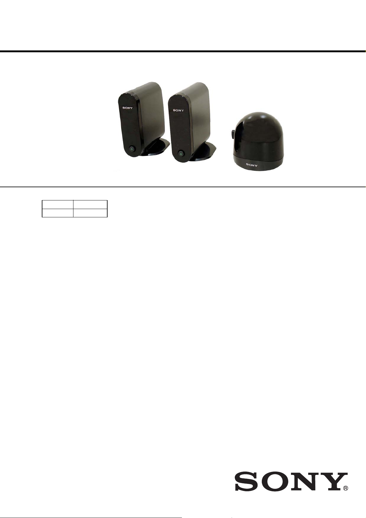
HWS-AV10T
• COMPONENT MODEL NAME FOR HWS-AV10K.
Transmitter HWS-AV10T
Receiver HWS-AV10R
Transmitter: HWS-AV10T
Video input: Impedance: 75 Ω
Level: 1 Vp-p
Audio input: Impedance: 81 kΩ
Level: 0.5 Vrms
Power consumption: Less than 240 mA
Power requirement: DC 6 V (supplied AC power adaptor)
Input terminal: Pin jack (Video, Audio L/R)
Output terminal: ø 3.5 mm monaural mini jack (IR Blaster)
Dimensions (w/h/d): approx. 2.7 × 4.9 × 4.3 inches
(approx. 68 × 124 × 110 mm)
Mass: approx. 6.7 oz (186 g)
Receiver: HWS-AV10R
Video output: Level: 1 Vp-p
Audio output: Level: 0.5 Vrms
Frequency response: 100 Hz - 20 kHz
Power consumption: Less than 260 mA
Power requirement: DC 6 V (supplied AC power adaptor)
Input terminal: 10-pin mini DIN jack (Dedicated antenna)
Output terminal: Pin jack (Video, Audio L/R)
Dimensions (w/h/d):
Main unit: approx. 2.7 × 4.9 × 4.3 inches
(approx. 68 × 124 × 110 mm)
Dedicated antenna:
approx. 3.4 × 3.2 × 3.2 inches
(approx. 86 × 82 × 82 mm)
(Cable length: approx. 39.4 inches/1 m)
Mass:
Main unit: approx. 5.8 oz (approx. 165 g)
Dedicated antenna:
approx. 4.7 oz (approx. 133 g)
HWS-AV10R
SPECIFICATIONS
US Model
DEDICATED
ANTENNA
General
Transmission frequency:
A/V signal Channel 1 : 2.415 GHz
Channel 2 : 2.429 GHz
Channel 3 : 2.443 GHz
Channel 4 : 2.457 GHz
Control signal 433.92 MHz
Max. communication range: Line of sight approx.100 ft. (30 m)
Operating temperature: 0°C to 40°C (32°F to 104°F)
Supplied accessories:
AC power adaptor (DC 6 V, 800 mA) (2), A/V cable
(approx. 39.4 inches/1 m, V/L/R y V/L/R) (2),
IR Blaster (1), Double sided seal (1), Operating instruc
tions (1), To enjoy clear images and sounds (1), Warranty
card (1)
Design and specifications are subject to change without notice.
9-887-109-01
2006B02-1
© 2006.02
HOME WIRELESS A/V SYSTEM
Sony Corporation
Personal Audio Division
Published by Sony Techno Create Corporation
Page 2

HWS-AV10K/AV10R/AV10T
Notes on chip component replacement
• Never reuse a disconnected chip component.
• Notice that the minus side of a tantalum capacitor may be
damaged by heat.
Unleaded solder
Boards requiring use of unleaded solder are printed with the lead
free mark (LF) indicating the solder contains no lead.
(Caution: Some printed circuit boards may not come printed with
the lead free mark due to their particular size.)
: LEAD FREE MARK
Unleaded solder has the following characteristics.
•Unleaded solder melts at a temperature about 40°C higher than
ordinary solder.
Ordinary soldering irons can be used but the iron tip has to be
applied to the solder joint for a slightly longer time.
Soldering irons using a temperature regulator should be set to
about 350°C.
Caution: The printed pattern (copper foil) may peel away if
the heated tip is applied for too long, so be careful!
• Strong viscosity
Unleaded solder is more viscous (sticky, less prone to flow)
than ordinary solder so use caution not to let solder bridges
occur such as on IC pins, etc.
• Usable with ordinary solder
It is best to use only unleaded solder but unleaded solder may
also be added to ordinary solder.
TABLE OF CONTENTS
Specifications ............................................................................ 1
1. GENERAL ................................................................... 3
2. DISASSEMBLY
2-1. Transmitter (HWS-AV10T), Receiver (HWS-AV10R) ... 4
3. DIAGRAMS ................................................................. 5
3-1. Printed Wiring Boards
– Transmitter Section (HWS-AV10T) – .......................... 7
3-2. Schematic Diagram
– Transmitter Section (HWS-AV10T) – .......................... 8
3-3. Printed Wiring Boards
– Receiver Section (HWS-AV10R) – .............................. 9
3-4. Schematic Diagram
– Receiver Section (HWS-AV10R) – .............................. 10
4. EXPLODED VIEWS
4-1. Transmitter Section (HWS-AV10T) ................................ 11
4-2. Receiver Section (HWS-AV10R) .................................... 12
4-3. Antenna Section .............................................................. 13
5. ELECTRICAL PARTS LIST .................................. 14
• Please repair transmitter (HWS-AV10T) and receiver (HWSAV10R) by the pair.
SAFETY-RELATED COMPONENT WARNING!!
COMPONENTS IDENTIFIED BY MARK ! OR DOTTED LINE WITH
MARK !ON THE SCHEMATIC DIAGRAMS AND IN THE PARTS
LIST ARE CRITICAL TO SAFE OPERATION.
REPLACE THESE COMPONENTS WITH SONY PARTS WHOSE
PA RT NUMBERS APPEAR AS SHOWN IN THIS MANUAL OR IN
SUPPLEMENTS PUBLISHED BY SONY.
2
Page 3
HWS-AV10K/AV10R/AV10T
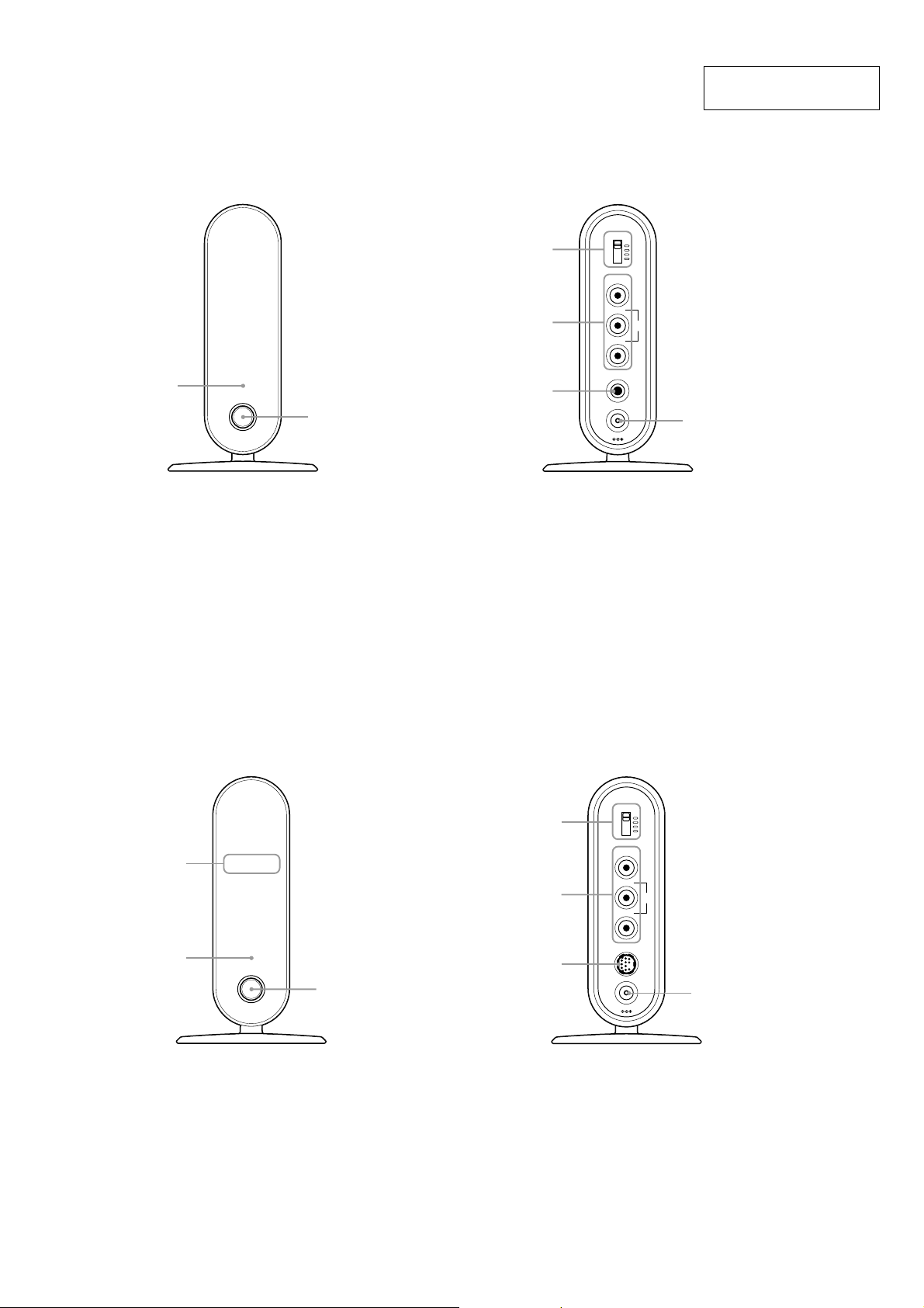
LOCATING THE CONTROLS
Transmitter
Front
1
1 Power indicator
Lights when the transmitter is turned on.
2 Power button
Turns the transmitter power on and off.
2
SECTION 1
GENERAL
Rear
3
4
5
3 CHANNEL switch*
Selects a desired channel (frequency) to
transmit.
4 VIDEO/AUDIO IN jacks
Connects the A/V cables to A/V
equipment in main room.
This section is extracted
from instruction manual.
CHANNEL
VIDEO IN
LEFT
AUDIO
IN
RIGHT
IR
EXTENDER
DC IN 6V
6
5 IR EXTENDER jack
Connects the IR Blaster (supplied).
Do not connect the other of supplied IR
Blaster.
6 DC IN 6V jack
Connects the AC power adaptor
(supplied).
* Make sure to set the CHANNEL switch of the
transmitter and receiver to the same position.
Receiver
Front
1
2
1 Infrared receiver
Receives the signal from the remote
control.
Point and operate the remote control of
A/V equipment at here.
2 Power indicator
Lights when the receiver is turned on.
3 Power button
Turns the receiver power on and off.
3
Rear
4
5
6
4 CHANNEL switch*
Selects a desired channel (frequency) to
receive.
5 VIDEO/AUDIO OUT jacks
Connects the A/V cables to your TV in
another room.
CHANNEL
VIDEO OUT
LEFT
AUDIO
OUT
RIGHT
ANT
b
DC IN 6V
7
6 ANT jack
Connects the dedicated antenna.
7 DC IN 6V jack
Connects the AC power adaptor
(supplied).
* Make sure to set the CHANNEL switch of the
transmitter and receiver to the same position.
3
Page 4
HWS-AV10K/AV10R/AV10T
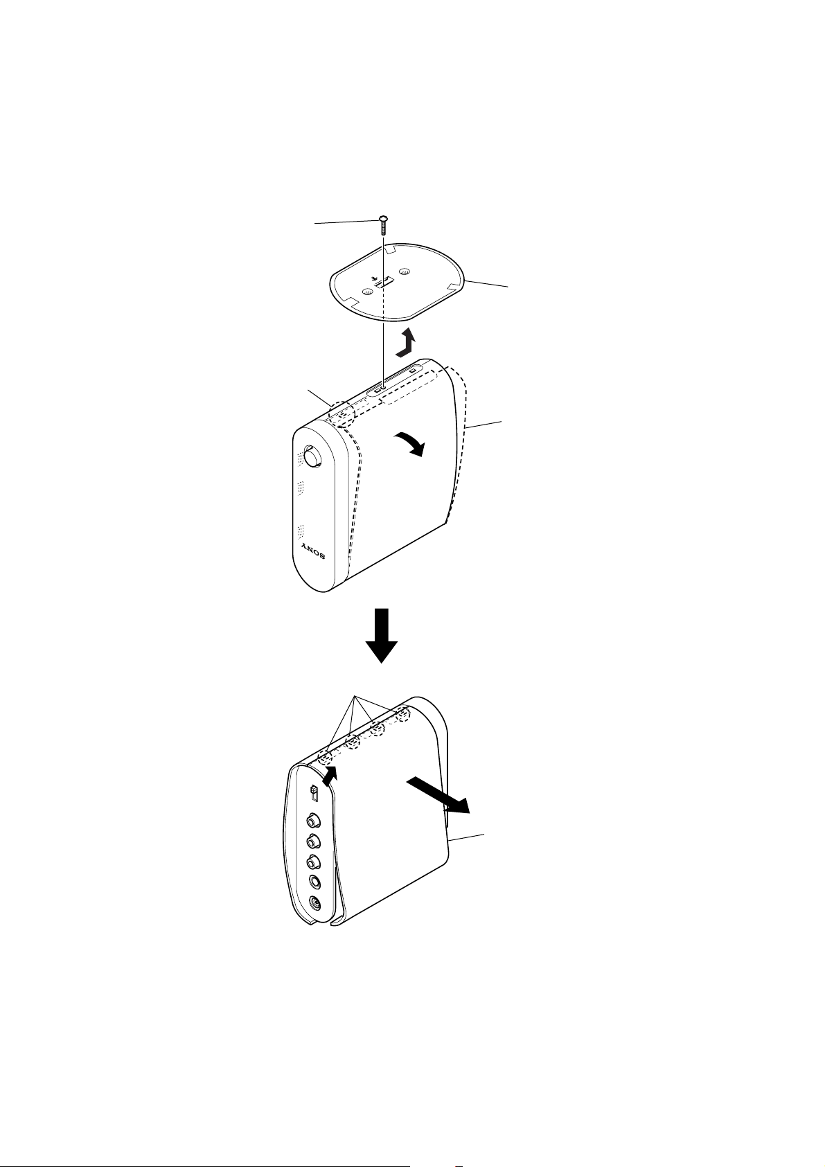
)
SECTION 2
DISASSEMBLY
• This set can be disassembled in the order shown below.
2-1. TRANSMITTER (HWS-AV10T), RECEIVER (HWS-AV10R)
1
screw
(+BVTP2.6)
2
3
claw
4
foot assy
cabinet (left
6
four claws
5
7
8
cabinet (left)
Note: Receiver (HWS-AV10R) is similarly removed through the illustration about Transmitter (HWS-AV10T).
4
Page 5

SECTION 3
DIAGRAMS
NOTE FOR PRINTED WIRING BOARDS AND SCHEMATIC DIAGRAMS.
HWS-AV10K/AV10R/AV10T
For schematic diagrams.
Note:
• All capacitors are in µF unless otherwise noted. (p: pF) 50 WV or
less are not indicated except for electrolytics and tantalums.
• All resistors are in Ω and 1/4 W or less unless otherwise specified.
•%: indicates tolerance.
• f : internal component.
• C : panel designation.
• A : B+ Line.
• Power voltage is dc 6 V and fed with regulated dc power supply
from dc in jack.
•Voltages are dc with respect to ground under no-signal conditions.
•Voltages are taken with a VOM (Input impedance 10 MΩ).
Voltage variations may be noted due to normal production tolerances.
For printed wiring boards.
Note:
• X : parts extracted from the component side.
• f : internal component.
• : Pattern from the side which enables seeing.
(The other layers' patterns are not indicated.)
Caution:
Parts face side: Parts on the parts face side seen from
(Side A) the parts face are indicated.
Pattern face side: Parts on the pattern face side seen from
(Side B) the pattern face are indicated.
• Indication of transistor.
C
Q
B
E
These are omitted.
5
Page 6
HWS-AV10K/AV10R/AV10T
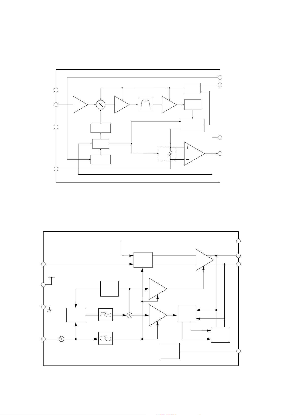
• IC BLOCK DIAGRAMS
– REMOCON R BOARD –
IC102 MICRF010YMTR
VSS
1
AGC
CONTROL
8
7
REFOSC
CAGC
ANT
2
VDD
3
CTH
4
– REMOCON T BOARD –
IC202 MICRF102YMTR
RF AMP
MIXER
SYNTHESIZER
CONTROL
LOGIC
REFERENCE
OSCILLATOR
IF AMP
SWITCHED-CAP
RESISTOR
IF AMP
SC
R
PEAK
DETECTOR
PROGRAMMABLE
L0W-PASS
FILTER
COMPARATOR
6
SHUT
DO
5
8
ASK
VDD
VSS
REF.OSC
7
TX
BIAS
VCO
CONTROL
BUFFER
BUFFER
REFERENCE
BIAS
ANTENNA
TUNING
CONTROL
PC
1
VDD
2
3
4
REFERENCE
OSCILLATOR
PHASE
DETECTOR
PRESCALER
DIVIDE
BY 32
POWER
AMP
VARACTOR
DEVICE
ANTP
6
ANTM
5
STBY
6
Page 7

HWS-AV10K/AV10R/AV10T
3-1. PRINTED WIRING BOARDS – TRANSMITTER SECTION (HWS-AV10T) –
3 4 5 6 7
FB104
TP106
TP102
TP103
TP100
TP101
FB102
ANTENNA
C100
BLK
YEL
BLU
WHT
RED
CABLE
11
7
1
R109
C115
4
5
8
1
IC102
2
C112
C111
R107
R110
C106
L103
IC101
1
3
C108
C114
C109
R106
5
4
L101
E
R103
C103
FB103
FB105
Q101
FB101
GND
ANT
1
A
BOARDREMOCON R
(SIDE A)
IC103
8
14
C113
B
R117
L106
C
C118
L104
R115
C116
1-869-899-
(11)
BOARDREMOCON R
X100
(SIDE B)
D
C110
E
C102
1-869-899-
11
(11)
TX-RF
BLOCK
: Uses unleaded solder.
BOARDJACK T
RED
WHT
BLU
YEL
BLK
RED
WHT
BLU
YEL
BLK
BRN
NAVY
WHT
RED
WHT
BLU
YEL
TP35
TP32
FB36
FB34
TP24
C22
TP22
TP21
TP20
TP31
FB30
FB31
TP23
TP28
TP25
TP26
TP27
FB22
TP33
TP36
TP34
FB32
FB21
FB33
FB35
C21
FL22
TP29
TP30
FB23
C20
FB20
FB24
FB29
FB26
FB27
FB28
FB25
R20
FL20
S20
2
4
6
8
10
FL21
1-869-896-
8
S20
CHANNEL
1
10
CN22
CN20
IR
CN21
DC IN 6V
2
VIDEO IN
LEFT
RIGHT
9
AUDIO IN
1
ttt
2
3
4
YEL
TP13
BLU
TP10
WHT
TP12
RED
TP11
FB13
FB12
FB11
BOARDPOWER SW
FB10
S10
D11
D10
(POWER)
R10
1-869-906-
11
(11)
1
3
5
7
9
K
EXTENDER
11
(11)
F
HWS-AV10K/AV10R/AV10T
77
Page 8

HWS-AV10K/AV10R/AV10T
3-2. SCHEMATIC DIAGRAM – TRANSMITTER SECTION (HWS-AV10T) –
S10
RB161L-40TE25
FB10
FB11
FB13
FB12
+6V
+6V
GND
GND
TP11
TP12
HT
RED
W
TP22
TP21
CHANNEL
TP13
YEL
TP31
FB22
FB21
FB23
S20
1
2
3
4
2
4
6
8
10
CN20
IR
EXTENDER
CN21
DC IN 6V
C20
470
10V
R20
82
TP10
BLU
TP20
FB20
1
3
5
7
9
• See page 6 for IC Block Diagrams.
D11
R10
470
D10
SLC-22MG3F
(POWER)
FB32
C22
470
10V
FB35
FB36
FB33
FB34
TP34
TP35
TP36
TP32
TP33
BLK
RED
YEL
WHT
BLU
TP106
TP101
TP102
TP100
TP103
EXIR
+5V
GND
+6V
GND
FB104
FB102
FB103
FB101
FB105
C100
1
C102
470
10V
C103
0.22
Q101
2SC4617R
BUFFER
R103
4.7k
CABLE
ANTENNA
IC101
TK11150CSCL-G
+5V REG
VIN
VOUT
CONT
GND
R106
4.7k
NP
C106
0.1
R107
1k
IC103
MC74HC00ADR2
CARRIER
FREQUENCY
C109
2p
L104
100nH
C108
0.22
L101
27nH
X100
13.4916MHz
R115
100k
C116
4.7
L106
39nH
R117
0
L103
27nH
C111
1
C114
100p
C115
C110
470
10V
VCC
1Y
2Y
3Y
4Y
GND
0.47
1A
1B
2A
2B
3A
3B
4A
4B
IC102
MICRF010YMTR
REMOTE CONTROL RECEIVER
VSS
ANT
VDD
CTH
R110
36k
R109
100k
C112
300p
C118
100p
REFOSC
C113
1
CAGC
SHUT
DO
CN22
VIDEO IN
LEFT
AUDIO
IN
RIGHT
HWS-AV10K/AV10R/AV10T
FL20
1
EMI
IN
GND
3
1
OUT
2
FL21
EMI
IN
GND
OUT
3
1
IN
C21
470
10V
2
FL22
EMI
GND
3
OUT
2
FB24
FB25
FB26
FB27
FB28
FB29
FB30
FB31
TP23
TP24
TP25
TP26
TP27
TP28
TP29
TP30
VIDEO
+6V
AUDIO-L
GND
AUDIO-R
GND
CH2
CH1
RED
BRN
BLU
YEL
BLK
WHT
NAVY
WHT
88
Page 9

HWS-AV10K/AV10R/AV10T
3-3. PRINTED WIRING BOARDS – RECEIVER SECTION (HWS-AV10R) –
1
2
3 4 5 6 7
A
BOARDREMOCON T
(SIDE A)
C206
3
1
IC201
5
4
L200
R204
C205
1
8
E
Q200
C212
R205
R200
R201
R202
C207
IC202
C203
4
5
C210
B
C200
C208
FB201
C202
C213
FB200
FB202
FB203
TP200
TP201
TP202
TP204
YEL
BLU
WHT
RED
: Uses unleaded solder.
BOARDJACK R
FB53
R46
FB49
FB51
FB50
C42
RED
WHT
BLU
YEL
TP45
TP44
TP43
TP47
C45
FL42
FL41
S40
2
4
6
8
10
1
3
5
7
9
C46
R40R41R42R43R44
K
CN40
S40
CHANNEL
2
10
VIDEO OUT
8
1
9
1
ttt
2
3
4
C43
LEFT
C
11
1-869-898-
BOARDREMOCON T
(SIDE B)
(11)
FL40
C41
AUDIO OUT
RIGHT
D
FB47
FB43
FB44
FB48
IC200
RED
3
E
1
X200
C209
C201
WHT
BLU
YEL
FB42
TP140
TP142
TP141
TP146
FB52
C44
FB41
FB40
C40
11
1-869-898-
(11)
C47
FB45
CN41
ANT
1-869-897-
11
(11)
CN42
DC IN 6V
YEL
BLU
WHT
RED
TP13
TP10
TP12
TP11
FB13
FB11
BOARDPOWER SW
FB10
FB12
S10
D11
D10
(POWER)
R10
1-869-906-
11
(11)
F
HWS-AV10K/AV10R/AV10T
99
Page 10

HWS-AV10K/AV10R/AV10T
3-4. SCHEMATIC DIAGRAM – RECEIVER SECTION (HWS-AV10R) –
S10
FB12
CN42
DC IN 6V
C40
470
10V
FB10
+6V
TP10
BLU
TP41
FB40
FB11
+6V
TP11
RED
TP40
FB42
R41
10k
R42
10k
R43
10k
R44
10k
GND
TP12
WHT
TP42
GND
TP13
YEL
TP46
R40
56k
FB13
RB161L-40TE25
FB52
FB41
1
3
5
7
9
• See page 6 for IC Block Diagrams.
D11
R10
470
D10
SLC-22MG3F
ER)
(POW
S40
CHANNEL
1
2
4
2
6
3
8
10
4
FB50
FB51
C46
C45
220
16V
R46
100
1
FB49
FB53
TP145
TP147
TP143
TP144
RED
W
BLU
YEL
IC202
MICRF102YMTR
REMOTE CONTROL TRANSMITTER
PC
0.1
C209
470
10V
VDD
VSS
REF.OSC
ASK
ANTP
ANTM
STBY
C210
3p
LOOP
ANTENNA
C212
5p
C205
100p
R204
100k
R205
C207
4.7
13.56MHz
C206
3k
X200
0.1
C208
0.22
C203
R202
47k
L200
39nH
Q200
R200
C202
0.22
10k
R201
10k
2SC4617R
INVERTER
IC201
TK11150CSCL-G
+5V REG
VIN
CONT
VOUT
GND
NP
FB202
FB201
FB200
FB203
VCC
GND
ROUT
C213
C200
0.1
1
C201
470
10V
IC200
RPM7140-H5
REMOTE
CONTROL
RECEIVER
TP204
TP202
HT
TP201
TP200
+5V
GND
+6V
GND
CN40
RIGHT
AUDIO
OUT
LEFT
VIDEO OUT
HWS-AV10K/AV10R/AV10T
C44
470
10V
FB45
FB47
FB44
FB43
FL41
EMI
GND
C41
100
10V
1
IN
3
2
OUT
FL42
EMI
GND
FB48
C43
100
10V
C47
1
1
IN
3
C42
470
10V
FL40
I
OUT
EM
GND
1
IN
3
2
OUT
2
NC
NC
NC
NC
+6V
CH1
AUDIO-R
+6V
VIDEO
AUDIO-L
CN41
10P
ANT
1010
Page 11

EXPLODED VIEWS
NOTE:
• -XX, -X mean standardized parts, so they may
have some differences from the original one.
• Items marked “*” are not stocked since they
are seldom required for routine service. Some
delay should be anticipated when ordering these
items.
4-1. TRANSMITTER SECTION (HWS-AV10T)
• The mechanical parts with no reference number
in the exploded views are not supplied.
• Accessories are given in the last of this parts
list.
HWS-AV10K/AV10R/AV10T
SECTION 4
not
supplied
5
6
2
3
12
4
13
not
supplied
7
11
8
1
8
not
supplied
9
8
Ref. No. Part No. Description Remarks
1 2-639-599-01 WINDOW (FRONT)
2 2-639-598-01 CABINET (LEFT) (TX)
3 1-479-698-11 TRANSMITTER (2.4G AV) (TX-RF BLOCK)
4 A-1134-055-A REMOCON R BOARD, COMPLETE
5 3-254-151-01 SCREW (B2.6), (+) P TAPPING
6 2-639-612-01 KNOB (SLIDE)
13
10
Ref. No. Part No. Description Remarks
7 2-639-597-01 CABINET (RIGHT) (TX)
8 2-581-618-02 FOOT, RUBBER
9 2-639-600-01 FOOT
10 3-254-140-01 SCREW (B2.6), (+) BV TAPPING
11 2-639-613-01 BUTTON (SW)
12 3-254-058-11 SCREW
13 3-255-655-01 SCREW (ST2 X 4)
11
Page 12

HWS-AV10K/AV10R/AV10T
4-2. RECEIVER SECTION (HWS-AV10R)
54
not
supplied
55
52
51
61
not
supplied
60
53
56
57
58
57
57
not
supplied
Ref. No. Part No. Description Remarks
51 2-639-599-01 WINDOW (FRONT)
52 2-682-796-01 CABINET (LEFT) (RX)
53 A-1134-058-A REMOCON T BOARD, COMPLETE
54 3-254-151-01 SCREW (B2.6), (+) P TAPPING
55 2-639-612-01 KNOB (SLIDE)
56 2-682-795-01 CABINET (RIGHT) (RX)
62
59
Ref. No. Part No. Description Remarks
57 2-581-618-02 FOOT, RUBBER
58 2-639-600-01 FOOT
59 3-254-140-01 SCREW (B2.6), (+) BV TAPPING
60 2-639-613-01 BUTTON (SW)
61 3-254-058-11 SCREW
62 3-255-655-01 SCREW (ST2 X 4)
12
Page 13

4-3. ANTENNA SECTION
HWS-AV10K/AV10R/AV10T
103
103
101
104
102
a
105
106
107
a
108
Ref. No. Part No. Description Remarks
101 2-639-607-01 KNOB (ANTENNA)
102 2-639-606-01 COVER (ANTENNA)
103 3-254-058-11 SCREW
104 2-639-609-01 HOLDER (LEFT)
105 2-639-608-01 HOLDER (RIGHT)
106 2-639-610-01 SPRING
109
110
110
111
Ref. No. Part No. Description Remarks
107 A-1134-006-A CASE ASSY (RX-RF BLOCK)
108 2-639-604-01 CASE (UPPER)
109 2-639-605-01 CASE (LOWER)
110 3-254-151-01 SCREW (B2.6), (+) P TAPPING
111 2-655-383-01 FOOT, RUBBER
13
Page 14

HWS-AV10K/AV10R/AV10T
JACK R JACK T
SECTION 5
ELECTRICAL PARTS LIST
NOTE:
• Due to standardization, replacements in the
parts list may be different from the parts
specified in the diagrams or the components
used on the set.
• -XX, -X mean standardized parts, so they
may have some difference from the original
one.
• Items marked “*” are not stocked since they
are seldom required for routine service.
Some delay should be anticipated when
ordering these items.
• CAPACITORS:
uF: µF
Ref. No. Part No. Description Remarks Ref. No. Part No. Description Remarks
JACK R BOARD
************
< CAPACITOR >
C40 1-104-652-11 ELECT 470uF 20% 10V
C41 1-126-933-61 ELECT 100uF 20% 16V
C42 1-104-652-11 ELECT 470uF 20% 10V
C43 1-126-933-61 ELECT 100uF 20% 16V
C44 1-104-652-11 ELECT 470uF 20% 10V
C45 1-126-934-11 ELECT 220uF 20% 16V
C46 1-115-156-11 CERAMIC CHIP 1uF 10V
C47 1-115-156-11 CERAMIC CHIP 1uF 10V
< CONNECTOR >
CN40 1-820-251-11 JACK, PIN 3P (AUDIO OUT, VIDEO OUT)
CN41 1-770-501-11 JACK 10P (ANT)
CN42 1-779-406-11 JACK, DC (POLARITY UNIFIED) (DC IN 6V)
< FERRITE BEAD >
FB40 1-481-092-11 INDUCTOR FERRITE BEAD
FB41 1-481-092-11 INDUCTOR FERRITE BEAD
FB42 1-481-092-11 INDUCTOR FERRITE BEAD
FB43 1-481-092-11 INDUCTOR FERRITE BEAD
FB44 1-481-092-11 INDUCTOR FERRITE BEAD
FB45 1-481-092-11 INDUCTOR FERRITE BEAD
FB47 1-481-092-11 INDUCTOR FERRITE BEAD
FB48 1-481-092-11 INDUCTOR FERRITE BEAD
FB49 1-481-092-11 INDUCTOR FERRITE BEAD
FB50 1-481-092-11 INDUCTOR FERRITE BEAD
FB51 1-481-092-11 INDUCTOR FERRITE BEAD
FB52 1-481-092-11 INDUCTOR FERRITE BEAD
FB53 1-481-092-11 INDUCTOR FERRITE BEAD
< FILTER >
FL40 1-234-561-21 FILTER, EMI REMOVAL (SMD)
FL41 1-234-561-21 FILTER, EMI REMOVAL (SMD)
FL42 1-234-561-21 FILTER, EMI REMOVAL (SMD)
• RESISTORS
All resistors are in ohms.
METAL: metal-film resistor
METAL OXIDE: Metal Oxide-film resistor
F: nonflammable
• COILS
uH: µH
•SEMICONDUCTORS
In each case, u: µ, for example:
uA...: µA... , uPA... , µPA... ,
uPB... , µPB... , uPC... , µPC... ,
uPD..., µPD...
R46 1-216-809-11 METAL CHIP 100 5% 1/10W
S40 1-786-950-11 SWITCH, SLIDE (CHANNEL)
************************************************************
C20 1-104-652-11 ELECT 470uF 20% 10V
C21 1-104-652-11 ELECT 470uF 20% 10V
C22 1-104-652-11 ELECT 470uF 20% 10V
CN20 1-563-836-21 JACK (IR EXTENDER)
CN21 1-779-406-11 JACK, DC (POLARITY UNIFIED) (DC IN 6V)
CN22 1-820-251-11 JACK, PIN 3P (AUDIO IN, VIDEO IN)
FB20 1-481-092-11 INDUCTOR FERRITE BEAD
FB21 1-481-092-11 INDUCTOR FERRITE BEAD
FB22 1-481-092-11 INDUCTOR FERRITE BEAD
FB23 1-481-092-11 INDUCTOR FERRITE BEAD
FB24 1-481-092-11 INDUCTOR FERRITE BEAD
FB25 1-481-092-11 INDUCTOR FERRITE BEAD
FB26 1-481-092-11 INDUCTOR FERRITE BEAD
FB27 1-481-092-11 INDUCTOR FERRITE BEAD
FB28 1-481-092-11 INDUCTOR FERRITE BEAD
FB29 1-481-092-11 INDUCTOR FERRITE BEAD
FB30 1-481-092-11 INDUCTOR FERRITE BEAD
FB31 1-481-092-11 INDUCTOR FERRITE BEAD
FB32 1-481-092-11 INDUCTOR FERRITE BEAD
FB33 1-481-092-11 INDUCTOR FERRITE BEAD
FB34 1-481-092-11 INDUCTOR FERRITE BEAD
FB35 1-481-092-11 INDUCTOR FERRITE BEAD
FB36 1-481-092-11 INDUCTOR FERRITE BEAD
The components identified by mark
0 or dotted line with mark 0 are
critical for safety.
Replace only with part number
specified.
When indicating parts by reference
number, please include the board.
< SWITCH >
JACK T BOARD
************
< CAPACITOR >
< CONNECTOR >
< FERRITE BEAD >
< RESISTOR >
R40 1-216-842-11 METAL CHIP 56K 5% 1/10W
R41 1-216-833-11 METAL CHIP 10K 5% 1/10W
R42 1-216-833-11 METAL CHIP 10K 5% 1/10W
R43 1-216-833-11 METAL CHIP 10K 5% 1/10W
R44 1-216-833-11 METAL CHIP 10K 5% 1/10W
14
< FILTER >
FL20 1-234-561-21 FILTER, EMI REMOVAL (SMD)
FL21 1-234-561-21 FILTER, EMI REMOVAL (SMD)
FL22 1-234-561-21 FILTER, EMI REMOVAL (SMD)
Page 15

HWS-AV10K/AV10R/AV10T
JACK T REMOCON R REMOCON T POWER SW
Ref. No. Part No. Description Remarks Ref. No. Part No. Description Remarks
< RESISTOR >
< VIBRATOR >
R20 1-216-808-11 METAL CHIP 82 5% 1/10W
< SWITCH >
S20 1-786-950-11 SWITCH, SLIDE (CHANNEL)
************************************************************
A-1134-055-A REMOCON R BOARD, COMPLETE
**************************
< CAPACITOR >
C100 1-115-156-11 CERAMIC CHIP 1uF 10V
C102 1-126-925-91 ELECT 470uF 20% 10V
C103 1-115-467-11 CERAMIC CHIP 0.22uF 10% 10V
C106 1-107-826-11 CERAMIC CHIP 0.1uF 10% 16V
C108 1-115-467-11 CERAMIC CHIP 0.22uF 10% 10V
C109 1-162-907-11 CERAMIC CHIP 2PF 0.25PF 50V
C110 1-126-925-91 ELECT 470uF 20% 10V
C111 1-125-837-91 CERAMIC CHIP 1uF 10% 6.3V
C112 1-164-389-11 CERAMIC CHIP 300PF 5% 50V
C113 1-125-837-91 CERAMIC CHIP 1uF 10% 6.3V
C114 1-162-927-11 CERAMIC CHIP 100PF 5% 50V
C115 1-113-619-11 CERAMIC CHIP 0.47uF 10V
C116 1-127-760-11 CERAMIC CHIP 4.7uF 10% 6.3V
C118 1-162-927-11 CERAMIC CHIP 100PF 5% 50V
< FERRITE BEAD >
FB101 1-481-092-11 INDUCTOR FERRITE BEAD
FB102 1-481-092-11 INDUCTOR FERRITE BEAD
FB103 1-481-092-11 INDUCTOR FERRITE BEAD
FB104 1-481-092-11 INDUCTOR FERRITE BEAD
FB105 1-481-092-11 INDUCTOR FERRITE BEAD
< IC >
IC101 6-705-337-01 IC TK11150CSCL-G
IC102 6-709-445-01 IC MICRF010YMTR
IC103 8-759-830-79 IC MC74HC00ADR2
< COIL >
L101 1-414-726-11 INDUCTOR 27nH
L103 1-414-726-11 INDUCTOR 27nH
L104 1-414-733-21 INDUCTOR 100nH
L106 1-414-728-21 INDUCTOR 39nH
< TRANSISTOR >
X100 1-813-767-11 VIBRATOR, CRYSTAL (13.4916MHZ)
************************************************************
A-1134-058-A REMOCON T BOARD, COMPLETE
**************************
< CAPACITOR >
C200 1-107-826-11 CERAMIC CHIP 0.1uF 10% 16V
C201 1-126-925-91 ELECT 470uF 20% 10V
C202 1-115-467-11 CERAMIC CHIP 0.22uF 10% 10V
C203 1-107-826-11 CERAMIC CHIP 0.1uF 10% 16V
C205 1-162-927-11 CERAMIC CHIP 100PF 5% 50V
C206 1-107-826-11 CERAMIC CHIP 0.1uF 10% 16V
C207 1-127-760-11 CERAMIC CHIP 4.7uF 10% 6.3V
C208 1-115-467-11 CERAMIC CHIP 0.22uF 10% 10V
C209 1-126-925-91 ELECT 470uF 20% 10V
C210 1-162-908-11 CERAMIC CHIP 3PF 0.25PF 50V
C212 1-162-910-11 CERAMIC CHIP 5PF 0.25PF 50V
C213 1-115-156-11 CERAMIC CHIP 1uF 10V
< FERRITE BEAD >
FB200 1-481-092-11 INDUCTOR FERRITE BEAD
FB201 1-481-092-11 INDUCTOR FERRITE BEAD
FB202 1-481-092-11 INDUCTOR FERRITE BEAD
FB203 1-481-092-11 INDUCTOR FERRITE BEAD
< IC >
IC200 6-600-129-01 IC RPM7140-H5
IC201 6-705-337-01 IC TK11150CSCL-G
IC202 6-709-452-01 IC MICRF102YMTR
< COIL >
L200 1-414-728-21 INDUCTOR 39nH
< TRANSISTOR >
Q200 8-729-927-99 TRANSISTOR 2SC4617R
< RESISTOR >
R200 1-216-833-11 METAL CHIP 10K 5% 1/10W
R201 1-216-833-11 METAL CHIP 10K 5% 1/10W
R202 1-216-841-11 METAL CHIP 47K 5% 1/10W
R204 1-216-845-11 METAL CHIP 100K 5% 1/10W
R205 1-216-865-11 METAL CHIP 3K 5% 1/10W
Q101 8-729-927-99 TRANSISTOR 2SC4617R
< RESISTOR >
R103 1-216-829-11 METAL CHIP 4.7K 5% 1/10W
R106 1-216-829-11 METAL CHIP 4.7K 5% 1/10W
R107 1-216-821-11 METAL CHIP 1K 5% 1/10W
R109 1-216-845-11 METAL CHIP 100K 5% 1/10W
R110 1-202-926-11 METAL CHIP 36K 5% 1/10W
R115 1-216-845-11 METAL CHIP 100K 5% 1/10W
R117 1-216-864-11 SHORT CHIP 0
< VIBRATOR >
X200 1-813-766-11 VIBRATOR, CRYSTAL (13.560MHZ)
************************************************************
POWER SW BOARD
**************
< DIODE >
D10 8-719-077-29 DIODE SLC-22MG3F (POWER)
D11 8-719-067-83 DIODE RB161L-40TE25
15
Page 16

HWS-AV10K/AV10R/AV10T
POWER SW
Ref. No. Part No. Description Remarks
< FERRITE BEAD >
FB10 1-481-092-11 INDUCTOR FERRITE BEAD
FB11 1-481-092-11 INDUCTOR FERRITE BEAD
FB12 1-481-092-11 INDUCTOR FERRITE BEAD
FB13 1-481-092-11 INDUCTOR FERRITE BEAD
< RESISTOR >
R10 1-216-817-11 METAL CHIP 470 5% 1/10W
< SWITCH >
S10 1-572-176-21 SWITCH, PUSH (1 KEY) (!)
************************************************************
MISCELLANEOUS
*************
3 1-479-698-11 TRANSMITTER (2.4G AV) (TX-RF BLOCK)
107 A-1134-006-A CASE ASSY (RX-RF BLOCK)
************************************************************
ACCESSORIES
***********
0 1-479-330-31 ADAPTOR, AC (AC-ES608K3)
1-759-586-22 CONTROLLER, VIDEO (AV MOUSE)
1-832-367-11 CORD, CONNECTION (AV)
(AUDIO/VIDEO CONNECTION CABLE)
2-674-819-01 MANUAL, INSTRUCTION (ENGLISH, SPANISH)
16
Page 17

MEMO
HWS-AV10K/AV10R/AV10T
17
Page 18

HWS-AV10K/AV10R/AV10T
REVISION HISTORY
Clicking the version allows you to jump to the revised page.
Also, clicking the version at the upper right on the revised page allows you to jump to the next revised
page.
Ver. Date Description of Revision
1.0 2006.02 New
 Loading...