

Sony HVRDR-60 Service manual
HVR-DR60
SERVICE MANUAL
Ver 1.2 2008.02
Revision History
Revision History
How to use
How to use
Acrobat Reader
Acrobat Reader
Revised-1
Replace the previously issued
SERVICE MANUAL 9-852-146-11
with this Manual.
US Model
Canadian Model
AEP Model
Chinese Model
Japanese Model
Link
Link
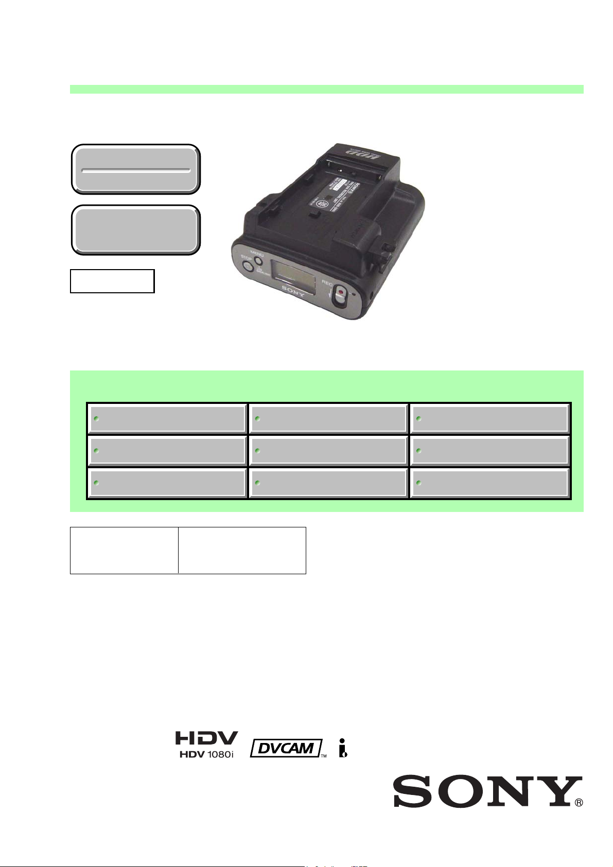
SPECIFICATIONS
SERVICE NOTE
DISASSEMBLY
The components identified by
mark 0 or dotted line with
mark 0 are critical for safety .
Replace only with part number specified.
BLOCK DIAGRAMS
FRAME SCHEMATIC DIAGRAM
SCHEMATIC DIAGRAMS
Les composants identifiés par une
marque 0 sont critiques pour la
sécurité.
Ne les remplacer que par une pièce
portant le numéro spécifié.
PRINTED WIRING BOARDS
REPAIR PARTS LIST
ADJUSTMENT
HVR-DR60
Sony EMCS Co.
HARD DISK RECORDING UNIT
2008B0800-1
© 2008.02
Published by Kohda TEC9-852-146-12

SPECIFICATIONS
System
File system FAT32
Hard disk 60 GB
The capacity is the value when 1 GB equals 1 billion bytes.
The actual usable capacity may be slightly less because administrative files etc. are included.
File format HDV recording MPEG-2TS (.m2t)
DVCAM/DV recording AVI-Type1 (.AVI)
RAW DV (.DV)
Input signal HDV recording/playback Video: MPEG-2TS
Audio: MPEG1 Audio Layer2 Stereo
DVCAM/DV recording/playback Video: DV embedded
Audio: PCM digital (12/16 bit, 32k, 48k)
Recording/playback time Approx. 270 minutes
General
Power requirement DC 7.2 V (battery pack)
DC 8.4 V (AC adaptor)
Power consumption 2.7 W
Operating temperature 0 °C to 40 °C (32 °F to 104 °F)
Storage temperature –20 °C to +60 °C (–4 °F to +140 °F)
Operating humidity 20 % (20 °C) to 90 % (35 °C) (no condensation)
Operating altitude Maximum 3,000 m (9,843 feet)
Dimensions Approx. 81 × 45 × 100 mm (w × h × d) (3 1/4 × 1 3/4 × 4 in.)
Mass Approx. 230 g (8 oz.)
Input/output jack i.LINK (IEEE1394 6-pin connector S400)
Included items i.LINK cable (6-pin – 4-pin) 70 cm (1)
Operating instructions (1)
Guide to supported models and their functions (1)
CD-ROM manual (1)
Shoe adaptor (1)
Optional accessories AC adaptor/charger AC-VQ1050B
Battery pack NP-F570/F770/F970
ENGLISH JAPANESE
ENGLISH JAPANESE
Design and specifications are subject to change without notice.
HVR-DR60
— 2 —

概略仕様
システム
ファイルシステム FAT32
ハードディスク 60GB
ファイルフォーマット
対応入力信号 HDV記録再生時 ビデオ: MPEG-2TS
録画/再生時間 約 270分
電源部、その他
電源電圧 バッテリー端子入力7.2V
消費電力 2.7 W
動作温度 0 °C~40 °C
保存温度
動作湿度
動作高度 海抜 3,000 m以下
外形寸法 約
本体質量 約 230 g
入力端子 i.LINK (IEEE1394 6 ピンコネクター s400)
付属品 i.LINKケーブル (6ピン –4ピン ) 約 70 cm (1)
別売アクセサリー ACアダプター /チャージャー AC-VQ1050B
本機の仕様および外観は、改良のため予告なく変更することがありますが、ご了承ください。
容量は、 1GBを 10億バイトで計算した場合の数値です。
また管理用ファイルなどを含むため、実際使用できる容量は若干減少する場合があります。
HDV記録時 MPEG-2TS (.m2 t)
DVCAM/DV記録時 AVI-Type1 (.AVI)
RAW DV (.DV)
オーディオ: MPEG1 Audio Layer2 Stereo
DVCAM/DV記録再生時 ビデオ: DV embedded
オーディオ: PCMデジタル (12/16 bit,32k,48k)
DC端子入力 8.4V
–20 °C~+60 °C
20 % (20 °C) ~90 (35 °C) % (結露がないこと )
81 × 45 × 100 mm (幅/高さ/奥行き )
保証書 (1)
取扱説明書 (1)
対応機種機能ガイド (1)
CD-ROMマニュアル (1)
シューアダプター (1)
バッテリーパック NP-F570/F770/F970
ENGLISH JAPANESE
ENGLISH JAPANESE
HVR-DR60
— 3 —
ENGLISH JAPANESE
ENGLISH JAPANESE
Danger of explosion if battery is incorrectly replaced.
CAUTION
Replace only with the same or equivalent type.
SAFETY-RELATED COMPONENT WARNING!!
COMPONENTS IDENTIFIED BY MARK 0 OR DO TTED LINE WITH
MARK 0 ON THE SCHEMATIC DIAGRAMS AND IN THE PARTS
LIST ARE CRITICAL TO SAFE OPERATION. REPLACE THESE
COMPONENTS WITH SONY PARTS WHOSE PART NUMBERS
APPEAR AS SHOWN IN THIS MANUAL OR IN SUPPLEMENTS
PUBLISHED BY SONY.
SAFETY CHECK-OUT
After correcting the original service problem, perform the following
safety checks before releasing the set to the customer.
1. Check the area of your repair for unsoldered or poorly-soldered
connections. Check the entire board surface for solder splashes
and bridges.
2. Check the interboard wiring to ensure that no wires are
"pinched" or contact high-wattage resistors.
3. Look for unauthorized replacement parts, particularly
transistors, that were installed during a previous repair. Point
them out to the customer and recommend their replacement.
4. Look for parts which, through functioning, sho w obvious signs
of deterioration. Point them out to the customer and
recommend their replacement.
5. Check the B+ voltage to see it is at the values specified.
6. Flexible Circuit Board Repairing
•Keep the temperature of the soldering iron around 270˚C
during repairing.
• Do not touch the soldering iron on the same conductor of the
circuit board (within 3 times).
• Be careful not to apply force on the conductor when soldering
or unsoldering.
ATTENTION AU COMPOSANT AYANT RAPPORT
À LA SÉCURITÉ!
LES COMPOSANTS IDENTIFÉS P AR UNE MARQ UE 0 SUR LES
DIAGRAMMES SCHÉMA TIQ UES ET LA LISTE DES PIÈCES SONT
CRITIQUES POUR LA SÉCURITÉ DE FONCTIONNEMENT. NE
REMPLACER CES COMPOSANTS QUE PAR DES PIÈSES SONY
DONT LES NUMÉROS SONT DONNÉS DANS CE MANUEL OU
DANS LES SUPPÉMENTS PUBLIÉS PAR SONY.
Unleaded solder
Boards requiring use of unleaded solder are printed with the leadfree mark (LF) indicating the solder contains no lead.
(Caution: Some printed circuit boards may not come printed with
the lead free mark due to their particular size.)
: LEAD FREE MARK
Unleaded solder has the following characteristics.
• Unleaded solder melts at a temperature about 40°C higher than
ordinary solder.
Ordinary soldering irons can be used but the iron tip has to be
applied to the solder joint for a slightly longer time.
Soldering irons using a temperature regulator should be set to
about 350°C.
Caution: The printed pattern (copper foil) may peel away if the
heated tip is applied for too long, so be careful!
• Strong viscosity
Unleaded solder is more viscous (sticky, less prone to flow) than
ordinary solder so use caution not to let solder bridges occur such
as on IC pins, etc.
•Usable with ordinary solder
It is best to use only unleaded solder but unleaded solder may
also be added to ordinary solder.
HVR-DR60
— 4 —
ENGLISH JAPANESE
ENGLISH JAPANESE
電池の交換は,正しく行わないと破裂する恐れがあり
注意
ます。電池を交換する場合には必ず同じ型名の電池
又は同等品と交換してください。
サービス,点検時には次のことにご注意下さい。
1. 注意事項をお守りください。
サービスのとき特に注意を要する個所については,
キャビネット,シャーシ,部品などにラベルや捺印で
注意事項を表示しています。これらの注意書き及び取
扱説明書等の注意事項を必ずお守り下さい。
2. 指定部品のご使用を
セットの部品は難燃性や耐電圧など安全上の特性を
持ったものとなっています。従って交換部品は,使用
されていたものと同じ特性の部品を使用して下さい。
特に回路図,部品表に0印で指定されている安全上重要
な部品は必ず指定のものをご使用下さい。
3. 部品の取付けや配線の引きまわしはもとどおりに
安全上,チューブやテープなどの絶縁材料を使用した
り,プリント基板から浮かして取付けた部品がありま
す。また内部配線は引きまわしやクランパによって発
熱部品や高圧部品に接近しないよう配慮されています
ので,これらは必ずもとどおりにして下さい。
4. サービス後は安全点検を
サービスのために取外したネジ,部品,配線がもとど
おりになっているか,またサービスした個所の周辺を
劣化させてしまったところがないかなどを点検し,安
全性が確保されていることを確認して下さい。
5. チップ部品交換時の注意
• 取外した部品は再使用しないで下さい。
• タンタルコンデンサのマイナス側は熱に弱いため交
換時は注意して下さい。
6. フレキシブルプリント基板の取扱いについて
• コテ先温度を270℃前後にして行って下さい。
• 同一パターンに何度もコテ先を当てないで下さい。
(3回以内)
• パターンに力が加わらないよう注意して下さい。
7. 無鉛半田について
無鉛半田を使用している基板には,無鉛(LeadFree)を
意味するレッドフリーマークがプリントされています。
(注意:基板サイズによっては,無鉛半田を使用して
いてもレッドフリーマークがプリントされて
いないものがあります)
:レッドフリーマーク
無鉛半田には,以下の特性があります。
• 融点が従来の半田よりも約40℃高い。
従来の半田こてをそのまま使用することは可能です
が,少し長めにこてを当てる必要があります。
温度調節機能のついた半田こてを使用する場合,約
350℃に設定して下さい。
注意: 半田こてを長く当てすぎると,基板のパター
ン(銅箔)がはがれてしまうことがあります
ので,注意して下さい。
• 粘性が強い
従来の半田よりも粘性が強いため,IC端子などが半田
ブリッジしないように注意して下さい。
• 従来の半田と混ぜて使用可能
無鉛半田には無鉛半田を追加するのが最適ですが,
従来の半田を追加しても構いません。
HVR-DR60
— 5 —

TABLE OF CONTENTS
Section Title Page
1. SERVICE NOTE
1-1. Service Note ···································································1-1
1-2. Description on Self-diagnosis Display ···························1-2
2. DISASSEMBLY
2-1. Disassembly ···································································2-2
3. BLOCK DIAGRAMS
3-1. Overall Block Diagram (1/2) ·········································3-1
3-2. Overall Block Diagram (2/2) ·········································3-2
3-3. Power Block Diagram ····················································3-3
4. PRINTED WIRING BOARDS AND
SCHEMATIC DIAGRAMS
4-1. Frame Schematic Diagram ·············································4-1
4-2. Schematic Diagrams·······················································4-3
4-3. Printed Wiring Boards ··················································4-13
4-4. Mounted Parts Location ···············································4-20
5. REPAIR PARTS LIST
5-1. Exploded Views······························································5-2
5-2. Electrical Parts List ························································5-6
6. ADJUSTMENT
6-1. Adjustment Items Required at Replacement
of Main Parts and Boards ···············································6-1
6-2. List of Service Tools ······················································6-2
6-3. Installation of Driver ······················································6-3
6-4. HDD Check ····································································6-7
6-5. HDD AVC Mode Recording Check ·····························6-10
6-6. Confirmation of HDV AVC Mode Playback ················6-10
6-7. Confirmation of DV SBP Mode Playback ···················6-10
6-8. Key Check ····································································6-11
6-9. LCD Indication Check ·················································6-11
6-10. Battery Check·······························································6-11
6-11. G-sensor Check ····························································6-12
6-12. HDD Format (File Erasure) ·········································6-12
6-13. History Clear ································································6-13
HVR-DR60
— 6 —
1. SERVICE NOTE
1-1. SERVICE NOTE
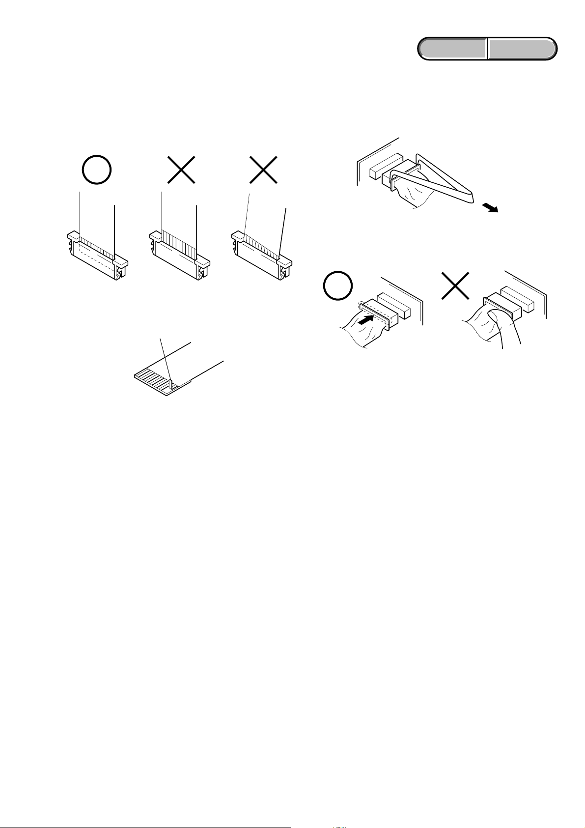
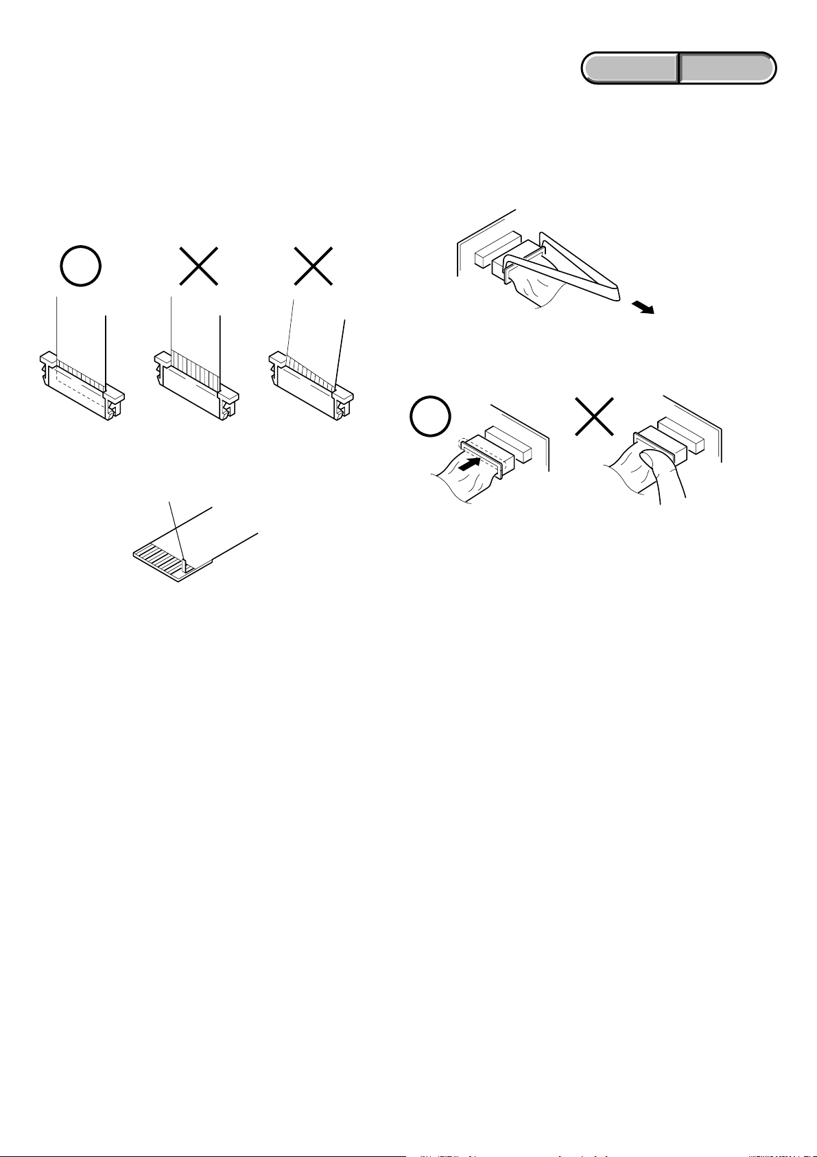
1. NOTE FOR REPAIR
Make sure that the flat cable and flexible board are not cracked of
bent at the terminal.
Do not insert the cable insufficiently nor crookedly.
Cut and remove the part of gilt
which comes off at the point.
(Take care that there are
some pieces of gilt left inside)
ENGLISH JAPANESE
ENGLISH JAPANESE
When remove a connector, don’t pull at wire of connector.
Be in danger of the snapping of a wire.
When installing a connector, don’t press do wn at wire of connector .
Be in danger of the snapping of a wire.
2. POWER SUPPLY DURING REPAIRS
In this unit, about 10 seconds after power is supplied to the battery terminal using the regulated power supply (8.4V),
the power is shut off so that the unit cannot operate.
This following method are available to prevent this.Take note of which to use during repairs.
Method 1.
Use the AC power adaptor.
HVR-DR60
1-1
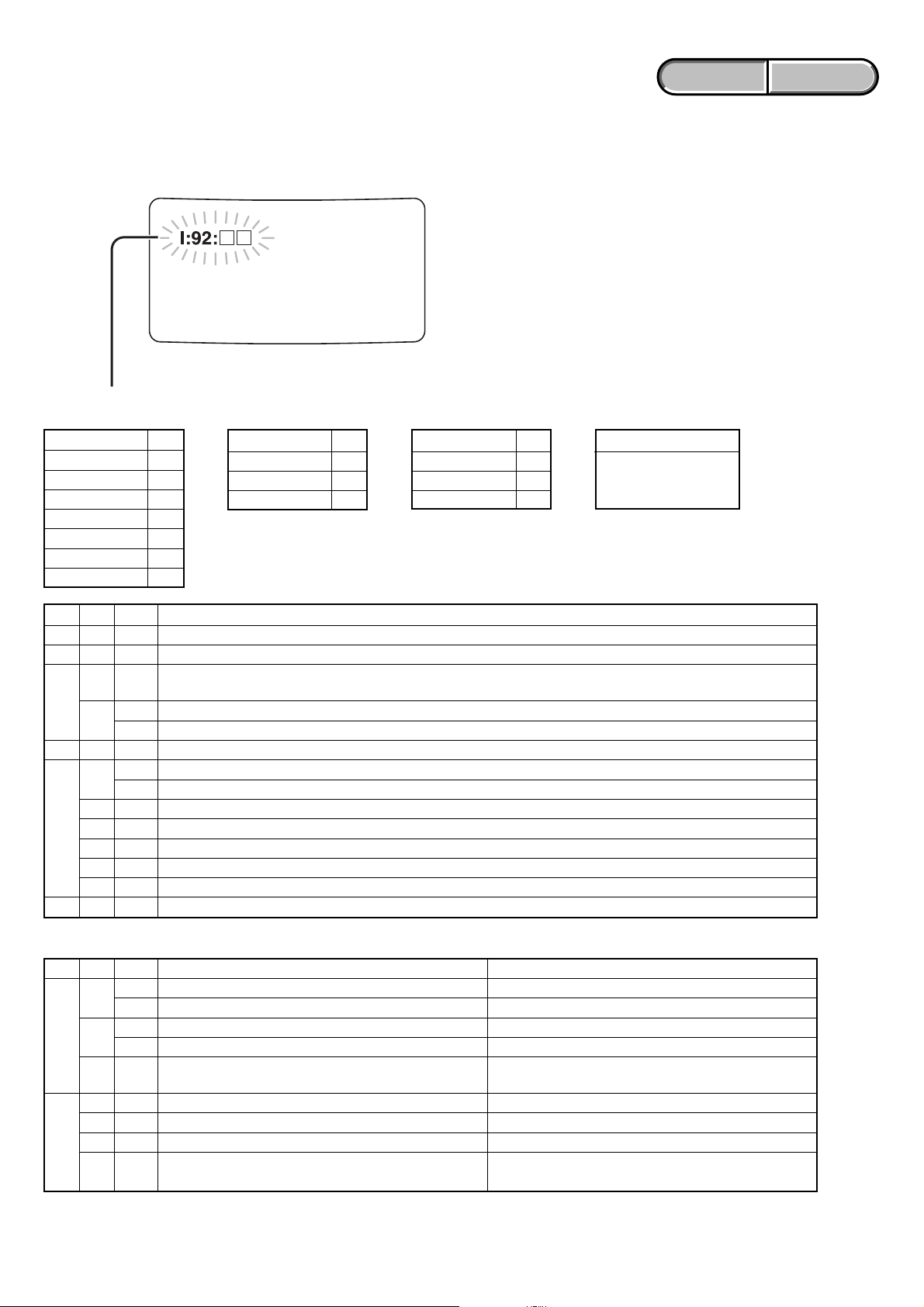
1-2. DESCRIPTION ON SELF-DIAGNOSIS DISPLAY
When an error occurs the following warning indicators may appear on the LCD screen.
And this unit is sent error code to camera.
Self-diagnosis display : X:Yy:ZZ
ENGLISH JAPANESE
ENGLISH JAPANESE
X
i.LINK I:
ATA A:
Power Supply P:
Button K:
MPEG/AVI M:
Other X:
Fatal Error F:
XYyZZDescription
I12ZZReturnable i.LINK-related error (The code that is corresponded to ZZ, is representative for status of i.LINK..)
A12ZZReturnable HDD-related error (The code that is corresponded to ZZ, is representative for error of ATA..)
12 ZZ
P
21
M12ZZStream processor abnormally (ZZ is given value. Such as, when AVI format is differed, ZZ becomes 01 etc.)
11
12 ZZ In case that error has been detected into file system etc.
F21ZZIn case that cannot communicates to Sub controller
22 ZZ In case that cannot controls the others device from Sub controller
91 ZZ Others, fatal error related with hardware
92 ZZ Others, fatal error related with software
X99ZZIn case that for DV SIGNAL PROCESSOR (IC501), error code etc. of firmware is to displaying.
Error is occurred when the power supply -related command is sent from Main controller to Sub controller. (ZZ is
given value)
01 In case that error has been occurred with power supply controller of each device using by Sub controller.
02 Cannot enter into sleep mode
01 HDD failure
02 i.LINK error
Y
Main 1y
Sub 2y
Other 9y
y
Physical Y1
Logical Y2
Other Y9
ZZ
When error is defined
in the devise, the error
code of it is displayed.
Principal Eroor Code
XYyZZ Countermeasure Description
01 Turn the unit back on again. Overflow of receiving buffer.
12
02 Turn the unit back on again. FAT error.
A90
F2001Turn the unit back on again. Unit failed PHY (Physical Layer) reset.
01 Store the unit at room temperature for a little Caution the unit to low temperature.
11 Store the unit at room temperature for a little Caution the unit to high temperature.
91 01
11 01 Turn the unit back on again. HDD has failed, or communication error between HDD.
12 01 Format the HDD HDD format error.
29 00
Turn the unit back on again. Detect the communication error with selecting the
There is partucularly no solution. (In this case, No writing into the sub controller firmware.
perform the firmware updates automatically.)
HVR-DR60
1-2
computer mode.

ENGLISH JAPANESE
ENGLISH JAPANESE
Following is error code that has been described to instructoin manual.
Display Code Countermeasure Cause
A:11:ss Turn this unit off and then back on. Cannot read or write to the HDD.
A:19:ss Turn this unit off and then back on. Internal error has occurred.
I:11:ss Turn this unit off and then back on. i.LINK communication error has occurred.
I:92:ss Turn this unit off and then back on. Internal error has occurred.
M:11:ss Turn this unit off and then back on. The recorded image cannot be manipulated.
X:ss:ss Turn this unit off and then back on. Internal error has occurred.
F:12:ss Format this unit by selecting DELETE and then FORMAT. There is a conflict in the HDD logic structure.
If you still cannot operate the unit, contact Sony Customer
Service.
F:29:ss Contact Sony Customer Service. There is an internal malfunction.
HVR-DR60
1-3
1. SERVICE NOTE
1-1. サービスノート
1. 修理時の注意
本フラットケーブルおよびフレキシブル基板の端子面に欠
け,折れ等がないことを確認する。
また,コネクタへの接続は,差し込み不足や斜め差しになら
ないように注意する。
ENGLISH JAPANESE
ENGLISH JAPANESE
コネクタを取り外す時に,線材部(極細)を持って引っ張る
と断線する恐れがありますので,絶対に線材部(極細)を
持って引っ張れないで下さい。
線材部(極細)を押さえながらコネクタを差し込むと,線材
部(極細)が断線する恐れがありますので,絶対に線材部
(極細)には負担をかけないで下さい。
先端の剥がれたメッキ部はカットして除去する。
(メッキ破片がコネクタ内に残っている場合もあるので注意)
2. 修理/調整時の電源供給について
本機では,安定化電源(8.4Vdc)からバッテリー端子に電源を供給した場合,約1 0 秒後にシャットオフし,動作しなくなりま
す。
これを避けるため,下記のいずれかの方法を用いてください。
方法1:
ACアダプタを使用する。
HVR-DR60
1-4
ENGLISH JAPANESE
ENGLISH JAPANESE
1-2. 自己診断表示について
エラーが発生した場合は,エラー内容に合わせて液晶表示画面にエラーコードが表示されます。
また,カメラ側にエラーコードが送信されます。
自己診断表示:X:Yy:ZZ
X
i.LINK I:
ATA A:
電源 P:
ボタン K:
MPEG/AVI M:
Other X:
致命的なエラー
XYyZZ エラー内容
I12ZZ復帰可能なi.LINK関連のエラー(ZZにあたる部分のコードは、i.LINKのステータスを返す)。
A12ZZ復帰可能なHDD関連エラー(ZZにあたる部分のコードは、ATAのエラーを返す)。
12 ZZ
21
M12ZZ
11
12 ZZ ファイルシステム等のエラー。
F21ZZSubコントローラーと通信できないとき。
22 ZZ Subコントローラーから他のデバイスを制御できないとき。
91 ZZ その他ハード関連の致命的なエラー。
92 ZZ その他ソフト関連の致命的エラー。
X99ZZDVSIGNALPROCESSOR(IC501)のファームウェアのエラーコード等を表示させたいとき。
F:
MainコントローラーからSubコントローラーに電源関連の命令を送信時に発生したエラー(ZZは任意
の値)。
01 Subコントローラーから各デバイスの電源制御時に発生したエラー。
02 スリープモードに入れなかったとき。
ストリームプロセッサ-のエラー(ZZは任意の値。例えば、AVIのフォーマットが違うときは01等。)。
01 HDD故障。HDD故障。
02 i.LINKエラー。
Y
Main 1y
Sub 2y
Other 9y
y
Physical Y1
Logical Y2
Other Y9
ZZ
デバイスにエラーの
規定があれば,その
コードを表示する。
主なエラーコード
XYyZZ 対処方法 原因
01 電源を再投入する。 受信バッファのオーバーフロー。
12
02 電源を再投入する。 FATの異常。
A
F2001電源を再投入する。 PHYのリセット失敗。
01 しばらく常温で保管する。 低温警告。
90
11 しばらく常温で保管する。 高温警告。
91 01 電源を再投入する。 コンピューターとの通信モード時にダウン検出。
11 01 電源を再投入する。 HDD故障,HDD間通信異常。
12 01 HDDのフォーマットを行う。 HDDフォーマットエラー。
29 00
特になし(ファームウェアの自動アップデートが Subコントローラーのファームウェアが書きこま
行われる)。 れていない。
HVR-DR60
1-5

ENGLISH JAPANESE
ENGLISH JAPANESE
下記は取扱説明書に記載されているエラーコードです。
表示コード 対処方法 原因
A:11:ss 本機の電源を切り,再度電源を入れなおしてください。HDDへの読み込み,または書き込みができません
でした。
A:19:ss 本機の電源を切り,再度電源を入れなおしてください。内部エラーです。
I:11:ss 本機の電源を切り,再度電源を入れなおしてください。i.LINKの通信エラーです。
I:92:ss 本機の電源を切り,再度電源を入れなおしてください。内部エラーです。
M:11:ss 本機の電源を切り,再度電源を入れなおしてください。記録動画を正しく処理できませんでした。
X:ss:ss 本機の電源を切り,再度電源を入れなおしてください。内部エラーです。
F:12:ss
F:29:ss コールセンターにお問い合わせください。 内部装置に異常があります。
メニュー設定画面で「DELETE」を選び,「FORMAT」
を選んで本機の初期化を行ってください。
初期化を行ってもだめな場合,コールセンターにお問
い合わせください。
HDD内の論理構造に矛盾を見つけました。
HVR-DR60
1-6E

NOTE FOR REPAIR
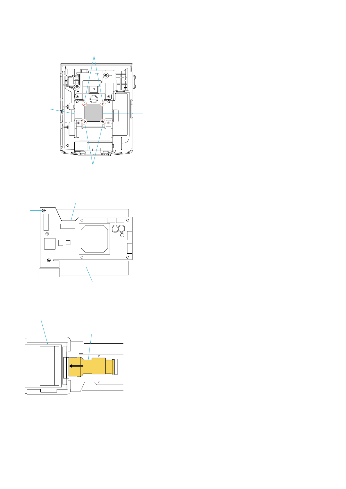
2. DISASSEMBLY
• Make sure that the flat cable and flexible board are not cracked of bent at the terminal.
Do not insert the cable insufficiently nor crookedly.
• When remove a connector, dont’ pull at wire of connector. It is possible that a wire is snapped.
• When installing a connector, dont’ press down at wire of connector.
It is possible that a wire is snapped.
Cut and remove the part of gilt
which comes off at the point.
(Be careful or some
pieces of gilt may be left inside)
HVR-DR60
2-1
EXPLODED VIEW
HELP
HELP
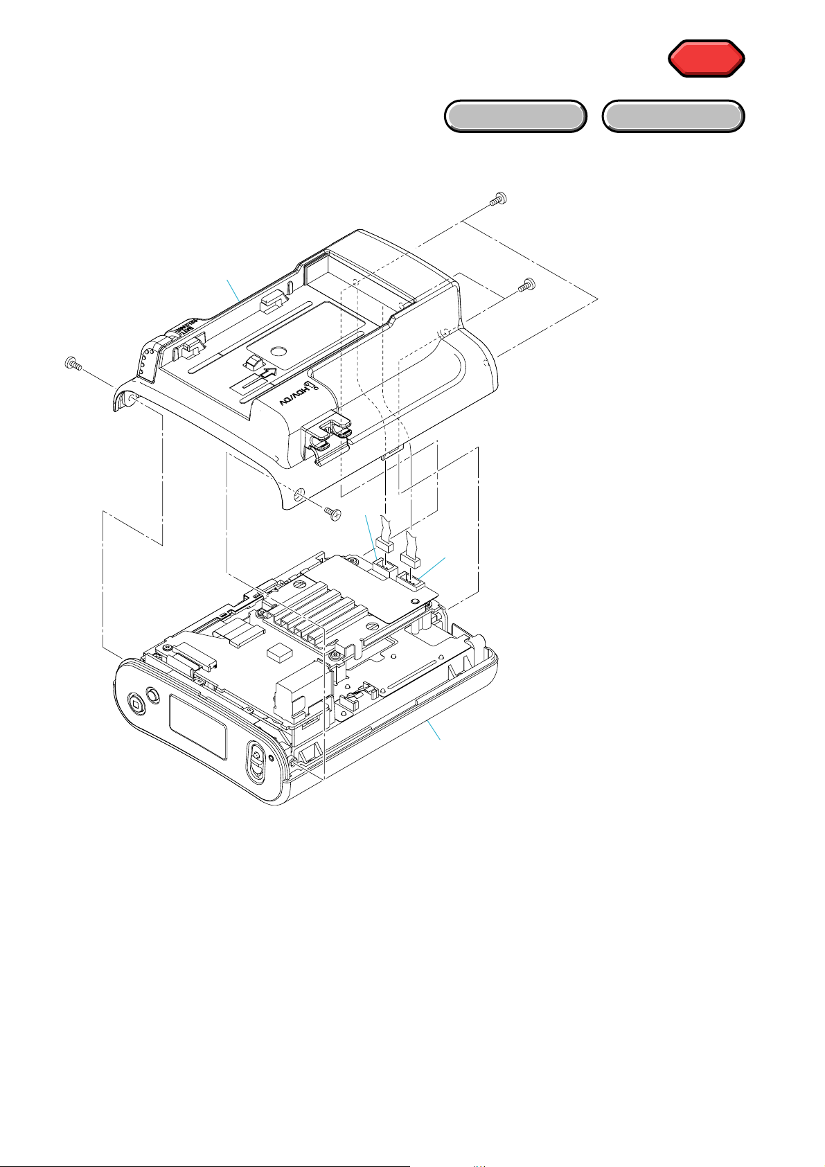
2-1. DISASSEMBLY
2-1-1. OVERALL ASSEMBLY
1
Bottom Case Block
1-1(#53)
HARDWARE LIST
1-4(#53)
1-3(#49)
1-6
1-2(#53)
1-5
HVR-DR60
2-2
2
Main Block
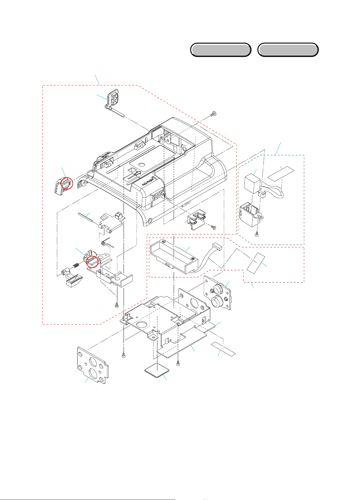
2-1-2. BOTTOM CASE ASSEMBLY
r
1
Bottom Case Block
1-1
EXPLODED VIEW
3-1(#49)
HARDWARE LIST
2
DC-IN Connecto
1-4(Clow)
1-6(Clow)
1-7
1-5
(#23)
1-3
(Boss)
4-1
1-2
(#53)
3-4
4
Board
3
Heatsink A
2-2
2-3
2-1(#23)
4-2
Battery Terminal
3-2(#23)
3-2(#23)
3-5
HVR-DR60
3-6
2-3
3-3
3-7
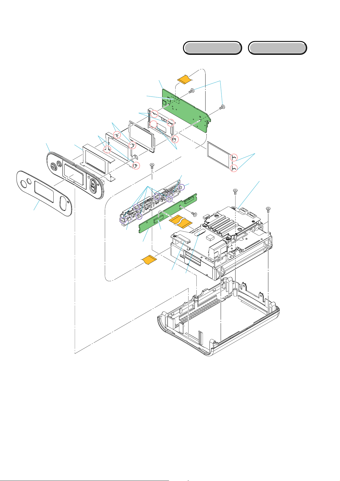
2-1-3. MAIN BLOCK
EXPLODED VIEW
k
HARDWARE LIST
1-10
1-1
1-6(Solder)
1-6(Solder)
1-5
1
LC-093 Board
1-7(Clow)
3-2(Clow)
1-3
3-1(#23)
3-4(Clow)
3-5
LC-093
1-9(Boss)
3-2(Clow)
SW-492
3-4(Clow)
3-3(#23)
1-4(#23)
2-2(#23)
1-8(Solder)
2
HDD Case Bloc
2-2 (#23)
3
SW-492
Board
1-2
2-1
HVR-DR60
2-4
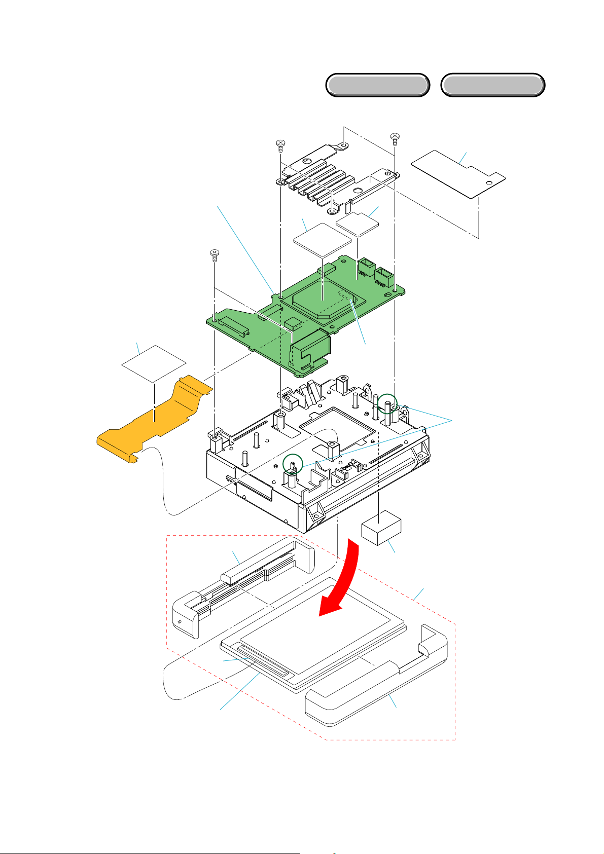
2-1-4. HDD CASE BLOCK
EXPLODED VIEW
HARDWARE LIST
2-7
2
HD-035 Board
2-4(#64)
2-2(#64)
2-2(#64)
2-1
2-9
2-3
HD-035
2-6
2-5(Boss)
1-3
1-2
1
HDD
HVR-DR60
2-5E
2-8
1-1
1-4
HELP
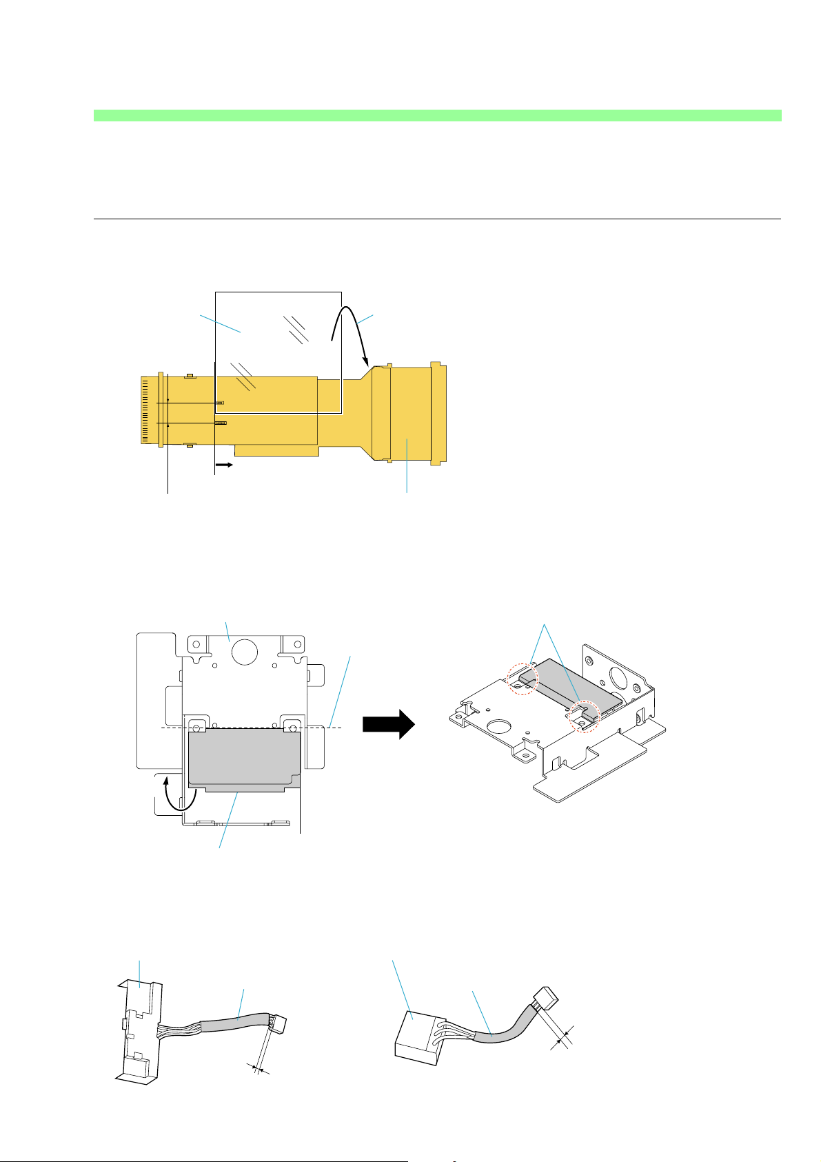
Sheet attachment positions and procedures of processing the flexible boards/harnesses are shown.
1. Attach the sheet (FP-431) to the FP-431 flexible cable of PWB by referring to the figure below.
Sheet (FP-431)
Tolerance: 0 to 2 mm
Reference
Attach the sheet starting from the
portion shown by the arrows.
Wind the sheet around the FP-431
mount.
FP-431 Mount.
2. Attach the sheet (heatsink A) to the heatsink A by referring to the figure below.
Attach the slit portion of the
Heatsink A
Attach the sheet
(Heatsink A) to
standard portion.
sheet to the bent portion.
Fold back
Sheet (Heatsink A)
3. Attach the harness sheet to the battery terminal board and DC-IN connector by referring to the figure below.
Cut the harness sheet into 40 x 40 mm square to use.
Battery Terminal Board
Harness Sheet Harness Sheet
1 to 3 mm
DC-IN Connector
HVR-DR60
1 to 3 mm
HELP
4. Attach the heat conduction sheet to the heatsink A by using four holes as a guide.
Holes
Heatsink A
Holes
Heat Conduction Sheet
5. Tighten two screws fixing the HDD board to the HDD case assembly in the order of numbers shown in the figure below.
HD-035 Board
2
1
HDD Case Assy
6. Insert the tip of FP-431 Flexible Board to the connector on HDD straight and firmly.
HDD
FP-431 Flexible Board
HVR-DR60
HELP
7. Attach the sheet (HD-035) sheet to the heatsink B fitting to the corner of connector.
Heatsink B
Sheet Bus (HD-035)
Connector
8. Insert the other end of FBH-002 connected to the SW-492 board to the connector on HD-035 board.
HD-035 Board
FBH-002
9. Place the FBH-002 cable connected to the LCD PWB board between the TOP CASE BLOCK ASSEMBLY and LCD PWB board.
Flexible Flat Cable (FBH-002)
LC-093 Board
Top Case Block Assy
10. Place the harnesses from the battery terminal board and DC-IN connector as shown in the figure below.
Harness of DC-IN Connector
Harness of Battery terminal board
HVR-DR60
HELP

3. BLOCK DIAGRAMS
Link
Link
OVERALL BLOCK DIAGRAM (1/2) POWER BLOCK DIAGRAM
OVERALL BLOCK DIAGRAM (2/2)
HVR-DR60
3. BLOCK DIAGRAMS
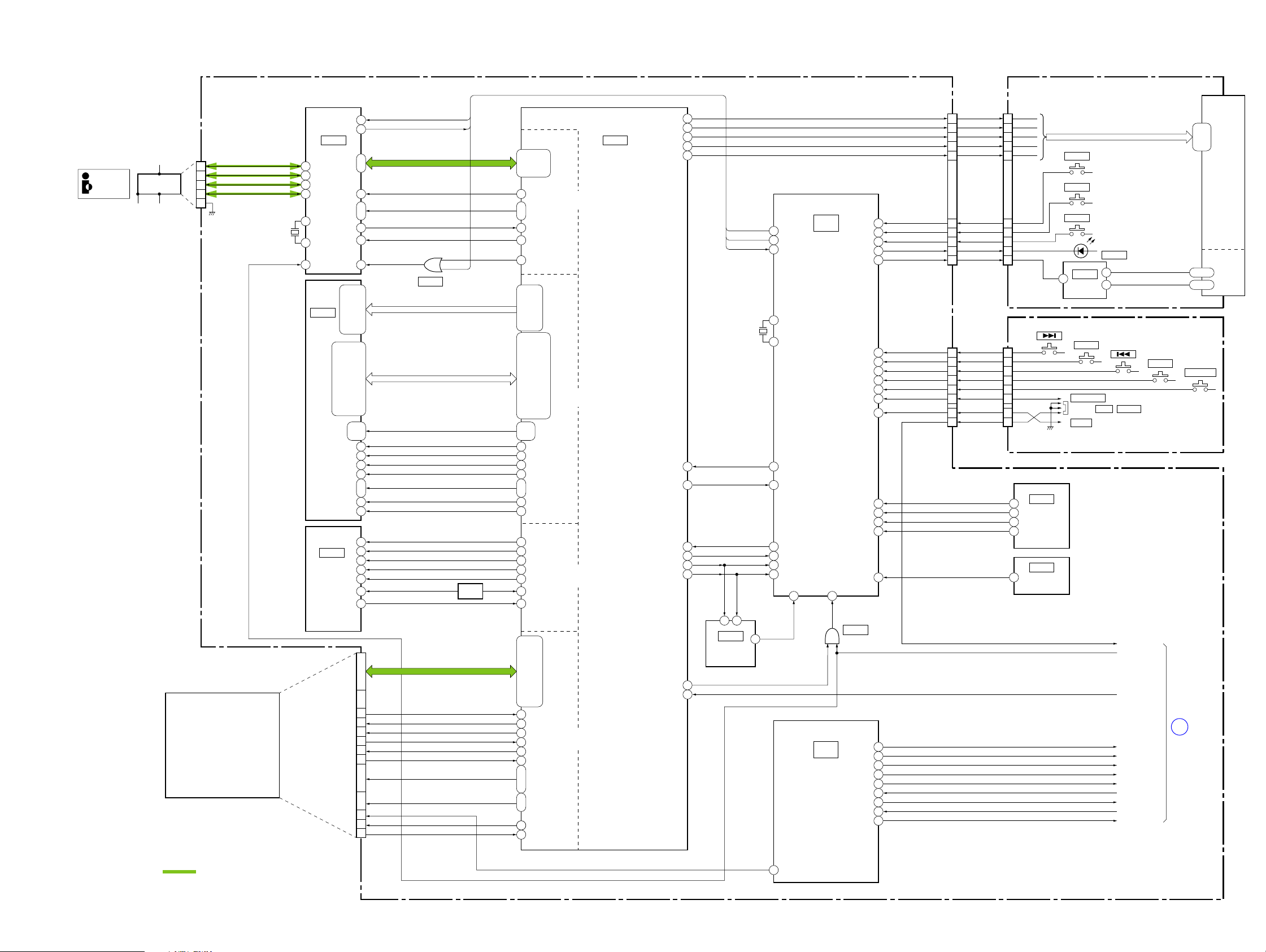
3-1. OVERALL BLOCK DIAGRAM (1/2)
HD-035 BOARD (1/2) LC-093 BOARD
34
35
36
37
59
60
53
PHY LINK
IC301
SDRAM
64M
(3/5)
MEMORY
HDV/DV
CN402
8
12
79
56
CN402
3
4
5
6
2
1.8 INCH HDD
(60GB)
TPBTPB+
TPATPA+
POR-
X401
24.576MHz
FP-431
FLEXIBLE BOARD
( ) : Number in parenthesis ( ) indicates the division number of schematic diagram where the component is located.
14
3
IC401
(4/5)
IC503
FLASH
(5/5)
6 - 134, 5
1
2
19
15
G7, H9, H3
G8, G9, F7, F3, G1
G2, G3, H1, H2, J3
A1, B1, R1, P1, E2, D2, C2, A2
C7, D7, M7, N7, A8, C8, D8, E8
L8, M8, N8, R8, A9, B9, P9, R9
R2, N2, M2, L2, D3, C3, N3, M3
F8, F2
K9, K1
J8 D1
J9
K7 F2
K8 G4
J7, H8
J2
J1
1
2
3
4
5
6
8
CN401
34 - 49
31
29
27
25
23
21
17, 19, 1614, 15
13
51
18
PD
CNA
LREQ
CTL0, CTL1
PCLK
LKON
LPS
4
LD0 - LD7
(IEEE 1394)
2
1
SUSPEND
IC402
(4/5)
DA0 - DA12
DDQ0 - DDQ31
DQM0 - DQM3
#CS
RAS
CAS
#WE
BA0, BA1
CLKE
CLKD
SI
SCLK
SRESET-
SCSSWE-
SD
DD0 - DD15
DMARQ
#DIOW-
#DIOR-
IORDY
#DMACK-
INTRQ
DA0 - DA2
#CS0-, #CS1-
HDD_NDASP
#RESET
#PDTAG
X503
27MHz
LPS
CLK
DV SIGNAL PROCESS
C7, A6
B7, A7
A10, A11
C11, B11
D7
C6
B12
A12
W2, W1, V2, U3, P4
D5, A3, B4, C5, A4, C8, B8, A8, D9, C10
H1, H3
E2
D2, E4 A5, B6
A17
C9
F18
E20
C19
E17
D19
L1
D20
W16, V16, T17, U20, T19
W15
V14
Y15
W14
W11
Y11
W9, Y10, V9U9, Y8
V10
M19
PHY LINK
INTERFACE
K1, J3, T2
R2, R1, P2, N2, M4
SDRAM
INTERFACE
J18, K19, R20, R19, U18, U19
A18, D16, C17, B17, A19, B19, B20, D18
C20, E18, E19, G17, G18, G19, H18, H20
G3, F1
FLASH ROM
INTERFACE
T18, V20, W17, Y17, V15
P19, N18, M18, N19, P20, T20
HDD
INTERFACE
IC501
(5/5)
E1
E3
F3
C2
B1
G1
C1
A20
C18
Y5
Y4
D3
V3
SUB_S_CNVSS
I2C_SDA
I2C_SCL
G_ALERT
SUB_TXD
SUB_RXD
56
IC202
LCD
EEPROM
(2/5)
PD
SUSPEND
CNA
X201
8MHz
7
SUB_S_RESET
LCD_RESET
LCD_CS1
LCD_A0
LCD_SDA
LCD_SCL
55
20
21
22
23
45
18
14
15
54
53
61 19
WP
IC203
(1/2)
SUB-CON
(2/5)
12
IC203
(2/2)
SUB-CON
(2/5)
CN203
15
13
11
9
7
EL_OFF
39
STOP
35
REC_ON
34
LED_ON
32
ENA
26
36
33
37
38
40
16
17
FF
PLAY
REW
REPEAT
CAM LINK
AVC_ON
SBP_ON
SW_OFF
5
4
3
2
17
CN201
22
33
44
5
6
8
9
7
CN601
#RES
15
#CS
13
A0
11 ND001
SDA
9
SCL
7
5
4
3
2
17
CN701
5
6
8
9
7
S706
S602
MENU
S601
STOP
S603
REC
3
LCD DRIVE
COMPUTER
VIDEO
IC601
S702
PLAY
D601
5
6
REC
S703
POWEROFF
S701
OUT1
OUT2
S704
REPEAT
26, 27
LND050
LND051
S705
CAM LINK
38, 39, 42
EL
SW-492 BOARD
1
2
3
62
58
4
IC212
(2/5)
AOZ
AOY
AOX
STBYB
VREF
3
4
5
10
6
SE201
G-SENSOR
(2/5)
IC213
2.5V REG
(2/5)
SW_OFF
POR-
MRESET
A
30
28
27
25
42
44
46
60
41
PWR_SUB_33
PWR_MAIN_33
PWR_HDD
PWR_LCD
PWR_P33
DCIN_AD
IB_ENABLE
BATT_AD
SLEEP
HD-035
BOARD (2/2)
(PAGE 3-2)
: VIDEO/AUDIO SIGNAL
08
HVR-DR60
31
3-1
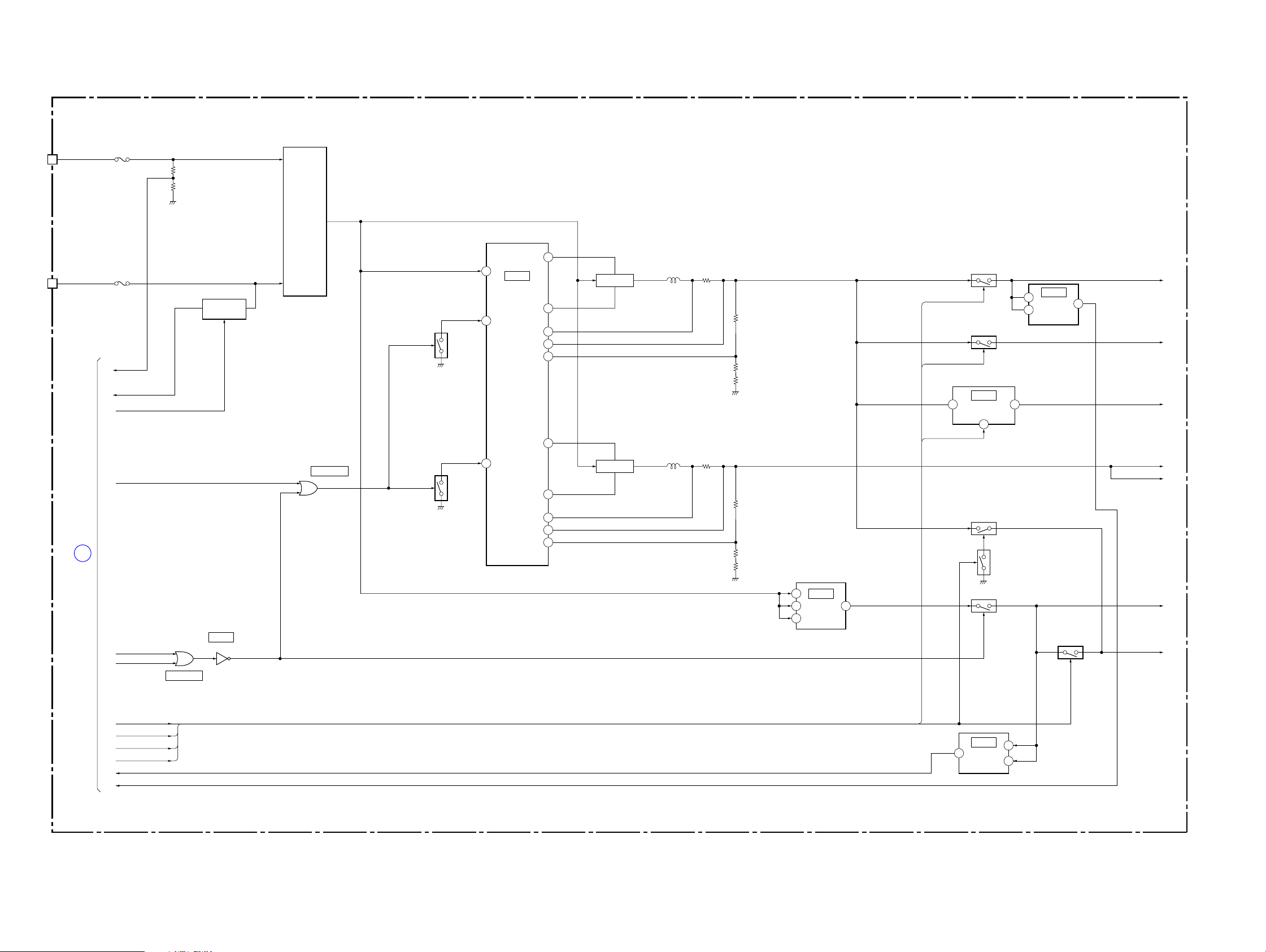
3-2. O VERALL BLOCK DIAGRAM (2/2) ( ) : Number in parenthesis ( ) indicates the division number of schematic diagram where the component is located.
HD-035 BOARD (2/2)
Q115, Q118
Q108, Q109
DC POWER
SELECT
SPWR
Q103
TG2
14
23
IC101
DC_DC
CONV.
(1/5)
13
BG2
18
12
11
9
SWTCHING
Q105
SENSE2+
SENSE2-
VOSENSE2
L101
1DC IN
1BATT IN
CN101
CN102
PLUS
BATT (+)
F101
F102
DCIN_AD
Q106, Q107
BATT
DATA
PWR_MAIN_33
PWR_HDD
Q111
Q110
MAIN M3.3V
IC110
2
RESET
4
1
GEN
(1/5)
HDD H3.3V
A
HD-035
BOARD (1/2)
(PAGE 3-1)
BATT_AD
IB_ENABLE
SLEEP
1SW_OFF
2PWR_SUB_33
IC116(2/2)
(1/5)
IC106
5
LCD POWER REG
(1/5)
TG1
26
L102
2
IC114
3.3V
5
6
REG.
(1/5)
3
Q102
28
BG1
22
30
31
1
IC116(1/2)
6SLEEP
(1/5)
5
3
IC115
(1/5)
42
7
SWTCHING
Q114
SENSE1+
SENSE1-
VOSENSE1
PWR_LCD
Q101
Q104
4
1
Q116
LCD 3.0V
Q117
1.8V
A1.8V
S3.3V
P3.3V
PWR_MAIN_33
PWR_HDD
PWR_P33
PWR_LCD
POR-
MRESET
08
HVR-DR60
3-2
PWR_P33
IC105
2
RESET
1
GEN
4
(1/5)
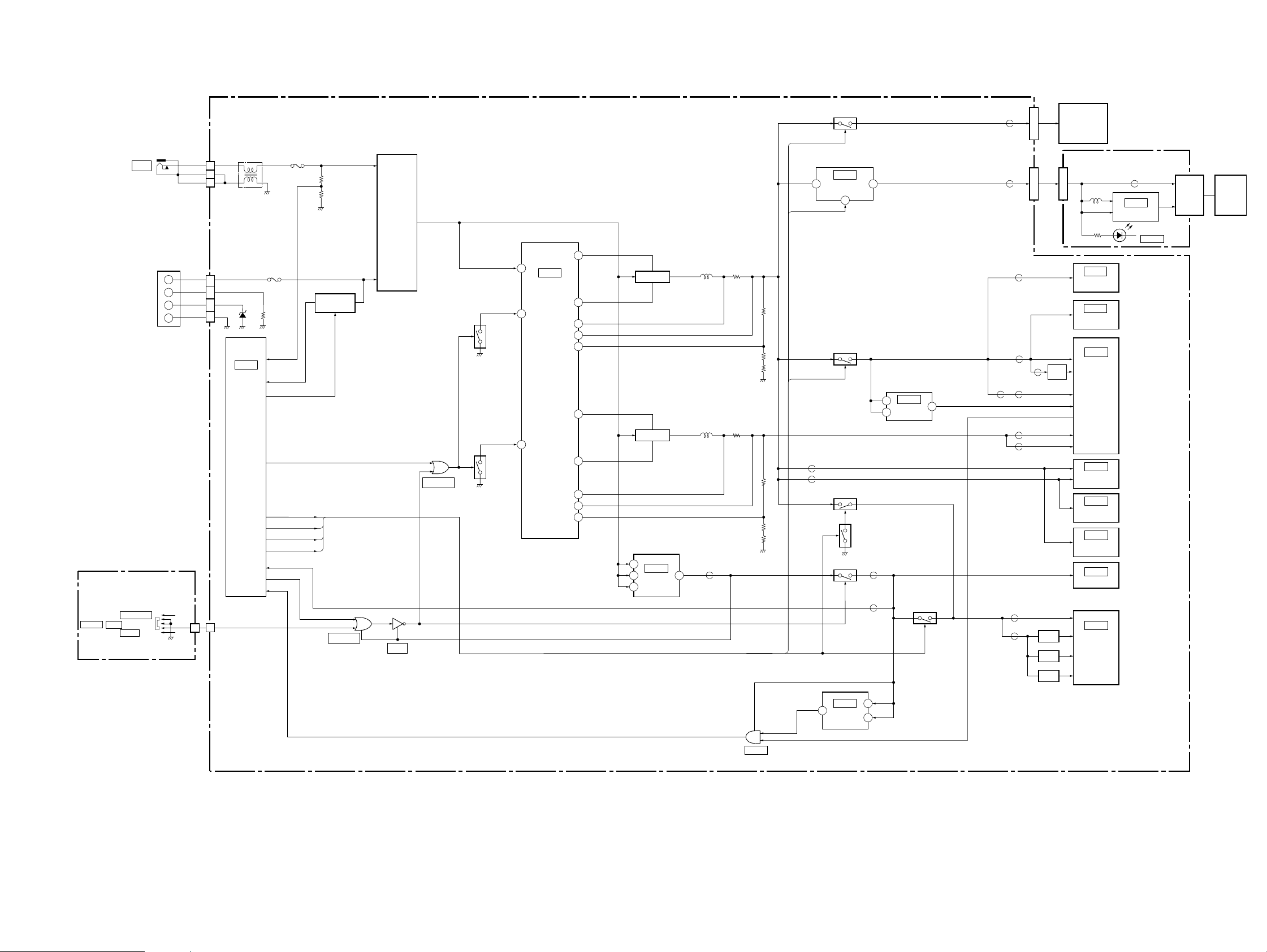
3-3. POWER BLOCK DIAGRAM
( ) : Number in parenthesis ( ) indicates the division number of schematic diagram where the component is located.
SW-492 BOARD
OFF
COMPUTER
VIDEO
S701
POWER
J001
DC IN
BH001
BATTERY
TERMINAL
3.3V
FB403
FB108
FB401
FB402
CN401
CN203
FB301
FB502
FB504FB106
FB102
FB501
5 - 1019,20
M3.3V
M3.3V
X503
27MHz
FB505
M3.3VA
MRESET
SUB_S_RESET
A1.8V
1.8V
FL401
FL402
FL403
1.8 INCH HDD
LC-093 BOARD
CN601
19,20
L601
IC301
SDRAM 64M
(3/5)
IC503
FLASH MEMORY
(5/5)
IC501
DV SIGNAL
PROCESS
(5/5)
SE201
G-SENSOR
(2/5)
IC202
LCD EEPROM
(2/5)
IC213
2.5V REG
(2/5)
IC402
AND GATE
IC401
PHY LINK
(4/5)
L602
IC601
LCD DRIVE
D601
REC
ND001
LCD901
LCD
MONITOR
IC106
LCD POWER REG
5
Q110
(1/5)
Q111
Q101
Q104
H3.3V
4
1
IC110
2
RESET GEN.
4
(1/5)
Q116
FB201
3.0V
MAIN M3.3V
1
A3.3V
S3.3V
Q117
P3.3V
HD-035 BOARD
Q115, Q118
CN101
1
2
3
1
2
3
4
7
CN102
CN201
BATT (+)
SUB-CON
LF101
IC203
(2/5)
D123
F101
F102
DCIN_AD
BATT_AD
IB_ENABLE
SLEEP
PWR_MAIN_33
PWR_HDD
PWR_P33
PWR_LCD
S3.3V
Q106, Q107
BATT
DATA
PWR_SUB_33
SW_OFF
IC116 (2/2)
(1/5)
2
1
PLUS
MINUS-A
MINUS-B
BATT(+)
+
SW
SIG
BATT(-)
−
CN701
7
Q108, Q109
DC POWER
SELECT
TG2
14
23
IC101
DC_DC
CONV.
(1/5)
13
Q103
28
6
5
3
IC116 (1/2)
(1/5)
452
7
8
IC115
(1/5)
Q102
BG2
18
12
11
9
TG1
26
BG1
22
30
31
1
SWTCHING
SENSE2+
SENSE2-
VOSENSE2
SWTCHING
SENSE1+
SENSE1-
VOSENSE1
2
5
6
Q105
Q114
IC114
3.3V REG.
(1/5)
L101
L102
FB109 FB112
3
PWR_HDD
PWR_LCD
PWR_MAIN_33
FB104
FB103
PWR_P33
HVR-DR60
3-3E
RESET GEN.
5
2
POR-
4
1
SUB_S_RESET
IC212
(2/5)
(1/5)
4
2
IC105
1
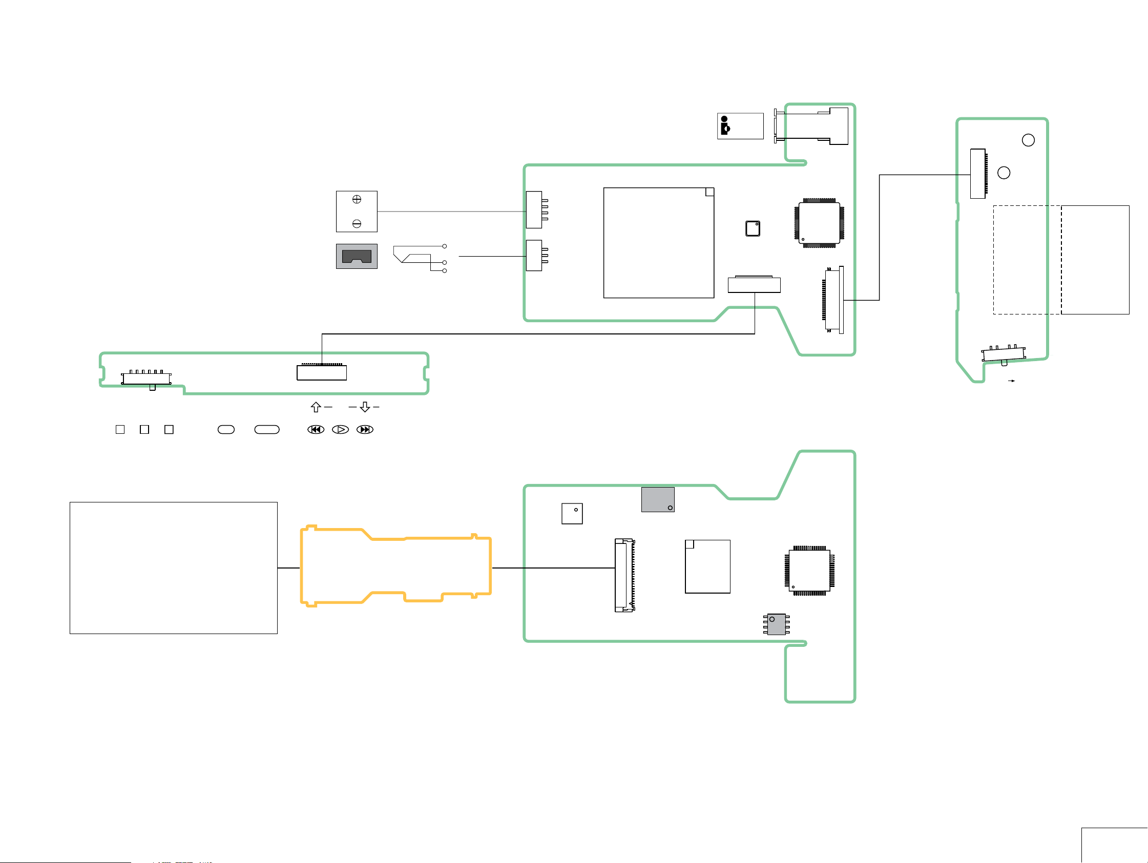
4-1. FRAME SCHEMATIC DIAGRAM
BATTERY
TERMINAL
DC IN
4. PRINTED WIRING BOARDS AND SCHEMATIC DIAGRAMS
HDV/DV
HD-035 BOARD (SIDE A)
4131
CN101 CN102
IC501
DV SIGNAL
PROCESS
SE201
G-SENSOR
SE201
120
CN201
CN402
49 32
IC401
64 17
LC-093 BOARD
(SIDE B)
12756
3
4
1 20
CN601
3348
65
161
201
CN203
S601
S602
ND001
S601
STOP
S602
MENU
LCD901
LCD MONITOR
SW-492 BOARD (SIDE B)
S701
POWER
OFF
S701
HDD
(1.8 INCH 60GB)
CAM LINK
S705
S603
1
REPEATCOMPUTER VIDEO
20
CN701
EXEC (MENU)
PLAY
S703 S702
S603
REC
S706S704
HD-035 BOARD (SIDE B)
5
4
IC503
FLASH MEMORY
FP-431
FLEXIBLE BOARD
8171
91632
IC101
24
25
CN401
IC503
8
1
(Not supplied)
51
IC301
64
1
IC202
LCD EEPROM
8
IC202
5
41
IC203
(Not supplied)
3348
3249
17
61
HVR-DR60
4-1
FRAME
 Loading...