

Sony HCD-DR3, HCD-DR330, HCD-XB200 Service manual

HCD-DR3/DR330/XB200
SERVICE MANUAL
HCD-DR3/DR330/XB200 is the tuner, dec k,
CD and amplifier section in LBT-DR3/
DR330/XB200.
Manufactured under license from Dolby Laboratories
Licensing Corporation.
“DOLBY” and the double-D symbol a are trademarks
of Dolby Laboratories Licensing Corporation.
CD
SECTION
T APE
DECK
SECTION
AEP Model
UK Model
HCD-XB200
E Model
HCD-DR3/DR330
Australian Model
HCD-DR3
Model Name Using Similar Mechanism HCD-G2500
Base Unit Type
Optical Pick-up Type KSS-213E/C2N
Model Name Using Similar Mechanism NEW
T ape Transport Mechanism Type CWL-44-RR
KSM-213ECM/C2NP
Amplifier section
(LBT -XB200)
DIN power output (Rated) 70W + 70W
(6 Ω at 1 kHz DIN)
Continuous RMS power output (Reference)
80W + 80W
(6 Ω at 1 kHz, 10%
THD)
Music power output (Reference)
140W + 140W
(6 Ω at 1 kHz, 10%
THD)
(LBT-DR330/DR3)
The following measured at AC 110/220V, 60Hz ;
Continuous RMS power output (Reference)
85W + 85W
(6 Ω at 1 kHz, 10%
THD)
DIN power output (Rated) 70W + 70W
(6 Ω at 1 kHz, DIN)
The following measured at AC 120/240V, 60Hz ;
Continuous RMS power output (Reference)
100W + 100W
(6 Ω at 1 kHz, 10%
THD)
DIN power output (Rated) 80W + 80W
(6 Ω at 1 kHz, DIN)
Inputs
PHONO IN (phono jack):
sensitivity 3mV,
impedance 47 kΩ
SPECIFICATIONS
SPECIFICATIONS
MD/VIDEO IN (phono jacks):
Outputs
PHONOS (stereo phono jacks):
MD/VIDEO OUT (phone jack):
SPEAKER: accepts impedance of 6 to
CD player section
System Compact disc and digital
Laser Semiconductor laser
Laser output Max. 44.6µW*
sensitivity 250mV,
impedance 47 kΩ
accepts headphones of 8 Ω
or more
voltage 250mV,
impedance 1 kΩ
16 Ω
audio system
(λ = 780 nm)
Emission
duration: continuous
*This output is the value
measured at a distance of
200 mm from the objective
lens surface on the Optical
Pock-up Block with 7 mm
aperture.
COMPACT Hi-Fi STEREO SYSTEM
Wavelength 780 – 790 nm
Frequency response 20Hz – 20kHz (±0.5 dB)
Signal-to-noise retio More than 90 dB
Dynamic range More than 90 dB
DIGITAL OUT
(Square optical connector jack, rear panel)
Wavelength 600 nm
Output Level –18 dBm
Tape deck section
Recording system 4-track 2-channel stereo
Frequency response (DOLBY NR OFF)
60 – 13,000 Hz (±3 dB),
using a Sony TYPE I
cassette
Tuner section
FM stereo, FM/AM superheterodyne tuner
FM tunr section
Tuning range 87.5 – 108.0 MHz
(50 kHz step)
Continued on next page
MICROFILM
AM tuner section
Tuning renge
European and Middle Eastern models:
531 – 1,602 kHz
(with the tuning interval set at 9 kHz)
Other models: 531 – 1,602 kHz
(with the tuning interval set at 9 kHz)
530 – 1,710 kHz
(with the tuning interval set at 10 kHz)
Antenna AM loop antenna,
External antenna terminals
Intermediate frequency 450 kHz
General
Power requirements
European model: 230 V AC, 50/60 Hz
Mexican model: 120V AC, 50/60 Hz
Australian model: 220 – 240 V AC, 50/60 Hz
Other models: 110 – 120 V or 220 – 240 V AC, 50/60 Hz Adjustable
with voltage selector
Power consumption
(HCD-DR330/DR3) 180W
(HCD-XB200) 135W
Dimensions(w/h/d) Approx. 355 × 425 × 442 mm
(14 × 163/4 × 171/2 in) incl.
projecting parts and controls
Mass Approx. 13.1 kg (28 lb 14 oz.)
Supplied accessories AM loop antenna (1)
Remote RM-SG7B (1)
FM wire antenna (1)
Design and specifications are subject to change without notice
MODEL IDENTIFICATION
Parts No.
PARTS No. MODEL
4-222-140-0π XB200 : AEP, UK
4-222-141-0π XB200 : EE, CIS
4-222-142-0π DR3 : E, SP, AR
4-222-143-0π DR3 : AUS
4-222-144-0π DR3 : MX
4-222-145-0π DR330
CAUTION
Use of controls or adjustments or performance of procedures
other than those specified herein may result in hazardous radiation
exposure.
Notes on chip component replacement
• Never reuse a disconnected chip component.
• Notice that the minus side of a tantalum capacitor may be
damaged by heat.
Flexible Circuit Board Repairing
• Keep the temperature of soldering iron around 270˚C
during repairing.
• Do not touch the soldering iron on the same conductor of the
circuit board (within 3 times).
• Be careful not to apply force on the conductor when soldering
or unsoldering.
Laser component in this product is capable
of emitting radiation exceeding the limit for
Class 1.
• Abbreviation
SP : Singapore model
MX : Mexican model
AR : Argentina model
AUS : Australian model
EE : East European model
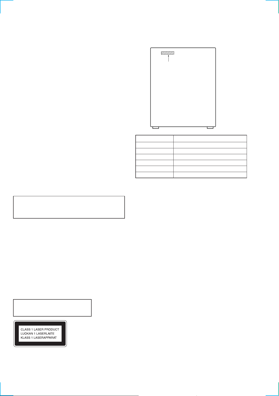
This appliance is classified as a CLASS 1 LASER product. The
CLASS 1 LASER PRODUCT MARKING is located on the rear
exterior.
The following caution label is located inside the unit.
2
SAFETY-RELATED COMPONENT WARNING!!
COMPONENTS IDENTIFIED BY MARK ! OR DO TTED LINE WITH
MARK ! ON THE SCHEMATIC DIAGRAMS AND IN THE PARTS
LIST ARE CRITICAL TO SAFE OPERATION. REPLACE THESE
COMPONENTS WITH SONY PARTS WHOSE PART NUMBERS
APPEAR AS SHOWN IN THIS MANUAL OR IN SUPPLEMENTS
PUBLISHED BY SONY.

TABLE OF CONTENTS
1. GENERAL ··········································································4
2. DISASSEMBLY
2-1. Top Cover ···········································································5
2-2. Front Panel Assy ································································· 5
2-3. Main Section······································································· 6
2-4. Main Board········································································· 6
2-5. CD Mechanism Deck Section ············································ 7
2-6. Tape Mechanism Deck Section ·········································· 7
2-7. Cassette Doors···································································· 8
2-8. CD Chassis Assy ································································ 8
2-9. Base Unit ············································································ 9
2-10. Turn Table ··········································································· 9
3. MECHANICAL ADJUSTMENTS ····························· 10
4. ELECTRICAL ADJUSTMENTS ······························· 10
5. DIAGRAMS
5-1. Ciecuit Boards Location··················································· 15
5-2. Block Diagrams································································ 16
Main Section····································································· 16
Tuner/CD Section····························································· 17
5-3. Printed Wiring Board Main Section ····························· 18
5-4. Schematic Diagram Main (1/3) Section ······················· 19
5-5. Schematic Diagram Main (2/3) Section ······················· 20
5-6. Schematic Diagram Main (3/3) Section ······················· 21
5-7. Printed Wiring Board AMP Section ····························· 22
5-8. Schematic Diagram AMP Section ································ 23
5-9. Printed Wiring Board CD Decoder Section ················· 24
5-10. Schematic Diagram CD Decoder Section ···················· 25
5-11. Printed Wiring Board Front Section····························· 26
5-12. Schematic Diagram Front (1/2) Section ······················· 27
5-13. Schematic Diagram Front (2/2) Section ······················· 28
5-14. IC Pin Function Description············································· 29
5-15. IC Block Diagrams ··························································· 31
6. EXPLODED VIEWS
6-1. Top Cover Section ···························································· 33
6-2. CD Door Section ······························································ 34
6-3. Panel Section ···································································· 35
6-4. Main Section····································································· 36
6-5. CD Mechanism Section···················································· 37
6-6. Base Unit Section (KSM-213ECM)································· 38
7. ELECTRICAL PARTS LIST······································· 39
3

SECTION 1
GENERAL
#§
%™
%¡
$∞
$¢
#£
#™
#¶
$¶$§
$™$¡ $£
$º#ª
#•
#∞#¢
1 %¢ %£
$ª$• %º
23 54
6
!ª
@™
7
!¶
8
9
0
!¡
!£!™
!§!∞!¢
!•
@¡@º
@£
#º#¡ @¢
1 1/u (POWER) button
2 TUNING MODE button
3 STEREO/MONO button
4 TUNER MEMORY button
5 ENTER/NEXT button
6 TUNER/BAND button
7 TUNING – button
8 TUNING + button
9 FUNCTION button
!º VOLUME knob
!¡ PHONES jack
!™ ª button (DECK B)
!£ · button (DECK B)
!¢ p button (DECK B)
!∞ 0 button (DECK B)
!§ ) button (DECK B)
!¶ P button (DECK B)
!• r REC button (DECK B)
@ª
@•
!ª CD SYNCHRO button
@º 0 button (CD)
@¡ ) button (CD)
@™ fl button (CD)
@£ p button (CD)
@¢ REPEAT button
@∞ PLAY MODE button
@§ AMS knob
@¶ DISC SKIP button
@• EDIT button
@ª DISC 5 button
#º DISC 4 button
#¡ DISC 3 button
#™ DISC 2 button
#£ DISC 1 button
#¢ DIRECTION button
#∞ DOLBY NR button
#§ p button (DECK A)
@¶
@§
@∞
#¶ 0 button (DECK A)
#• ) button (DECK A)
#ª ª button (DECK A)
$º · button (DECK A)
$¡ GROOVE button
$™ DBFB button
$£ SURROUND button
$¢ SPECTRUM ANALYZER button
$∞ DISPLAY/DEMO button
$§ ROCK button
$¶ POPS button
$• JAZZ button
$ª SALSA button
%º FLAT button
%¡ t /CLOCK SET button
%™ SLEEP button
%£ TIMER REC button
%¢ DAILY button
4

SECTION 2
DISASSEMBLY
Note : Follow the disassembly procedure in the numerical order given.
2-1. TOP COVER
1
Three screws
3
Top cover
1
Three screws
2-2. FRONT PANEL ASSY
2
Harness
(CN302)
9
Front panel assy
8
Board to board connector
(CN602)
(CN601)
1
Connector
(to deck A)
7
Screw
2
Seven screws
6
Four screws
4
Connector
(to deck B)
5
Connector
(CN702)
3
Connector board
(CN11)
5
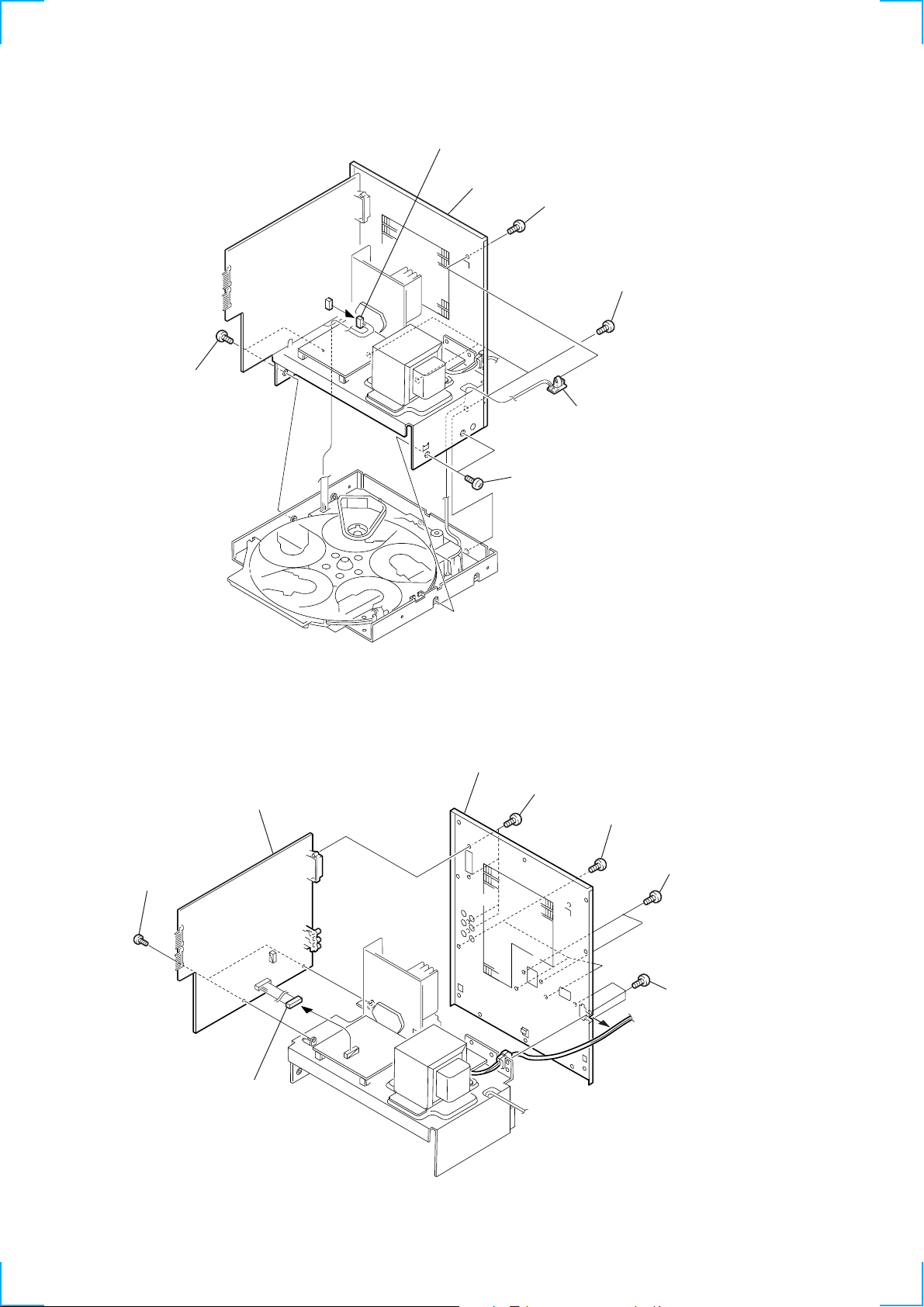
2-3. MAIN SECTION
6
Two screws
1
Connector
(CN301)
7
Main section
2
Screw
5
Two screws
4
Three screws
3
Photo Socket board
2-4. MAIN BOARD
7
Two screws
8
Main board
6
Connector
(CN701)
5
Rear panel
1
Four screws
2
Three screws
3
Four screws
4
Three screws
6

2-5. CD MECHANISM DECK SECTION
4
CD mechanism
deck section
3
Four screws
2
Holder, wire
2-6. TAPE MECHANISM DECK
1
Flexible flat cable
(to connector 16pin
on tape mechanism deck)
2
Six screws
1
Two screws
3
Tape mechanism deck
7

2-7. CASSETTE DOORS
)
Cassette door (L)
(Note: Four claws are used.)
Cassette door (R)
(Note: Four claws are used.
2-8. CD CHASSIS ASSY
!™
2
Connector
(CN606)
!¡
CD key board
4
six claws
!º
Three screws
CD chassis assy
Remove the
8
5
AMS knob
6
7
Three screws
Nut
Washer
1
(CN603)
Connector
9
AMS board
3
Five screws
8

2-9. BASE UNIT
t
e
1
Connector
(CN02)
4
Boss
2
Connector
(CN01)
5
Base uni
2-10. TURN T ABLE
Note:
When the disc table is installed, adjust the positions of
roller can and mark ” as shown in the figure, then set
to the groove of disc table.
A
1
Screw
2
Bracket (BU)
1
Screw
3
Yoke bracket
3
Step screw
4
Turn tabl
A
9

SECTION 3
MECHANICAL ADJUSTMENTS
SECTION 4
ELECTRICAL ADJUSTMENTS
Precaution
1. Clean the following parts with a denatured alcohol-moistened
swab:
record/playback head pinch rollers
erase head rubber belts
capstan idlers
2. Demagnetize the record/playback head with a head
demagnetizer.
3. Do not use a magnetized screwdriver for the adjustments.
4. After the adjustments, apply suitable locking compound to the
parts adjusted.
5. The adjustments should be performed with the rated power
supply voltage unless otherwise noted.
Torque Measurement
Torque
FWD
FWD
back tension
FF/REW
Torque meter
CQ-102C
CQ-102C
CQ-201B
Meter reading
40 to 70 g • cm
(0.56 - 0.97 oz • inch)
1 to 5 g • cm
(0.01 - 0.07 oz • inch)
55 to 140 g • cm
(0.76 - 1.94 oz • inch)
DECK SECTION 0 dB=0.775V
1. Demagnetize the record/playback head with a head
demagnetizer.
2. Do not use a magnetized screwdriver for the adjustments.
3. After the adjustments, apply suitable locking compound to the
parts adjusted.
4. The adjustments should be performed with the rated power
supply voltage unless otherwise noted.
5. The adjustments should be performed in the order given in this
service manual. (As a general rule, playback circuit adjustment
should be completed before performing recording circuit
adjustment.)
6. The adjustments should be performed for both L-CH and RCH.
Tape
P-4-A100
WS-48B
Record/Playback Head Azimuth Adjustment
(Deck A, Deck B)
Note: Perform this adjustments for both decks.
Procedure:
1. Mode : Playback
Signal
10 kHz, –10 dB
3 kHz, 0 dB
Used for
Azimuth Adjustment
Tape Speed Adjustment
test tape
P-4-A100
(10kHz, –10dB)
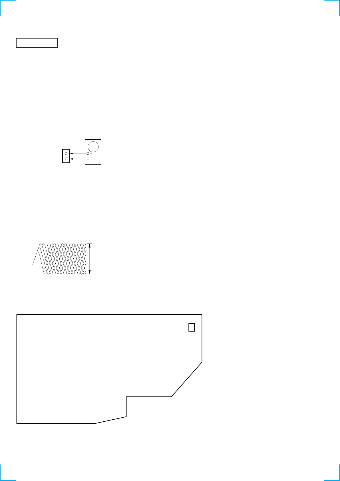
2. Turn the adjustment scre w and check output peaks. If the peaks
do not match for L-CH and R-CH, turn the adjustment screw
so that outputs match within 2 dB of peak.
L-CH
peak
screw
position
output
level
R-CH
peak
SPEAKER
terminal (JK703)
set
within
2dB
L-CH
peak
R-CH
peak
level meter
within 2dB
screw
position
10

e
r
3. Mode: Playback Tape Speed Adjustment (Deck A)
test tape
P-4-A100
(10kHz, –10dB)
in phase 45˚ 90˚ 135˚ 180˚
SPEAKER
terminal (JK703)
(L-CH)
L
R
SPEAKER
terminal (JK703)
(R-CH)
Waveform of oscilloscope
good wrong
oscilloscop
4. After the adjustments, apply suitable locking compound to the
parts adjusted.
Procedure:
1. Mode: Playback
test tape
WS-48B
(3kHz, 0dB)
set
SPEAKER
terminal (JK703)
frequency counte
+
–
2. Adjust the SFR601 so that the frequency counter reads 3,000
Hz ± 90Hz.
Adjustment Location: FRONT board
Sample Value of Wow and flutter
W. RMS (JIS) within 0.3%
(test tape: WS-48B)
Adjustment Location: FRONT board
[FRONT BOARD] — Component side —
Adjustment Location:
Remove the cassette lid before adjustment (See page 8)
Adjustment screws
PB head (deckA)
or REC/PB head (deck B)
SFR601
IC603
TAPE SPEED
CN603
11

TUNER SECTION 0 dB=1µV
r
AM T uning Volta ge Adjustment
Main board
TP1
G
VT
DC voltmete
+
–
Procedure:
1. Set the reception frequency of the unit to 530 kHz.
2. Adjust L105 for 1.2 ± 0.05 V reading on the DC voltmeter.
3. Set the reception frequency of the unit to 1,710 kHz.
4. Confirm that the voltage reading on the DC voltmeter is within
8.0 ± 0.5 V.
Adjustment Location: MAIN board (See page 13)
AM T racking Adjustment
loop antenna
AM RF SSG
loop antenna
(Supplied accessories)
set
30% amplitude
modulation by
400 Hz signal
Field strength dB (
Procedure:
1. Tune the set to 600 kHz.
2. Set the output of AM RF SSG so that the input level of the set
will become 60 dB (µV/m).
3. Adjust L104 so that when the waveform on the oscilloscope is
maximum, no noise appears.
4. Tune the set to 1,400 kHz.
60 cm
µ
V/m) =SSG output level dB (µV/m) –26 dB.
AM ANTENNA
terminal (TM1)
5. Adjust TC102 so that when the waveform on the oscilloscope
is maximum, no noise appears.
• Repeat the procedures in each adjustment several times, and the
tracking adjustment should be finally done by the trimmer
capacitors.
Adjustment Location: MAIN board (See page 13)
12

FM Tuned Level Adjustment
FM RF SSG
Ω
coaxial
75
set
Carrier frequency : 98 MHz
Modulation : AUDIO 1 kHz, 75 kHz
deviation (100%)
Output level : 28 dB (at 75 W open)
FM ANTENNA terminal
(JK101)
Procedure:
1. Supply a 28 dB 98 MHz signal from the ANTENN A terminal.
2. Tune the set to 98 MHz.
3. Adjust SFR101 to the point (moment) when the TUNED
indicator will change from going off to going on.
Adjustment Location: MAIN board
Adjustment Location
[MAIN BOARD] — Component side —
IC102
FM T uned Level
AM T rac king
L105
AM T uning Voltage
SFR101
L104
TC102
TP1
JK101
13
CD SECTION
V
Note:
1. CD Block is basically constructed to operate without
adjustment. Therefore, check each item in order given.
2. Use YEDS-18 disc (3-702-101-01) unless otherwise indicated.
3. Use an oscilloscope with more than 10MΩ impedance.
4. Clean the object lens by an applicator with neutral detergent
when the signal level is low than specified value with the
following checks.
5. Adjust the focus bias adjustment when optical pick-up block is
replaced.
RF Level Check
CD DECODER
board
TP01
RF
VC
oscilloscope
Procedure :
1. Connect oscilloscope to test point TP01 on CD DECODER
board.
2. Turned Power switch on.
3. Put disc (YEDS-18) in and playback.
4. Confirm that oscilloscope waveform is clear and check RF
signal level is correct or not.
Note: Clear RF signal waveform means that the shape “◊” can be
clearly distinguished at the center of the waveform.
VOLT/DIV: 200 m
TIME/DIV: 500 nS
level: 1.0 Vp-p
+0.3
–0.2
Adjustment Location:
[CD DECODER BOARD] — Component side —
14
TP01
(VC)

SECTION 5
d
DIAGRAMS
5-1. CIRCUIT BOARDS LOCATION • Wavef orm
TR board
MAIN board
POWER (AMP) board
POWER SUPPLY board
THIS NOTE IS COMMON FOR PRINTED WIRING
BOARDS AND SCHEMATIC DIAGRAMS.
(In addition to this necessary note is printed in each
block.)
For schematic diagrams.
MAIN BOARD
IC103 @™
1
Note:
CONNECTOR board
LED board
CD KEY board
CD SW board
PHOTO SOCKET board
AC SWITCH board
REM board
FRONT board
VR board
H/P board
AMS board
• All capacitors are in µF unless otherwise noted. pF: µµF
50 WV or less are not indicated except for electrolytics
and tantalums.
• All resistors are in Ω and 1/
specified.
• % : indicates tolerance.
¢
•
• 2 : nonflammable resistor.
• 1 : fusible resistor.
• C : panel designation.
• U : B+ Line.
• V : B– Line.
• H : adjustment for repair.
• Voltages and waveforms are dc with respect to ground
• Voltages are taken with a VOM (Input impedance 10 M Ω).
• Waveforms are taken with a oscilloscope.
• Circled numbers refer to waveforms.
• Signal path.
: internal component.
The components identified by mark ! or dotted
line with mark ! are critical for safety.
Replace only with part number specified.
under no-signal (detuned) conditions.
Voltage var iations may be noted due to normal produc-
tion tolerances.
F : FM
f : AM
E : PB (DECK A)
d : PB (DECK B)
G : REC (DECK B)
J : CD
g : MD/VIDEO
i : PHONO
4
W or less unless otherwise
L809 5
5
L809 6
6
FRONT BOARD
IC601 !§
2
CD DECODE BOARD
IC01 #£
3
7.2 MHz
111.7 kHz
111.0 kHz
6 MHz
3.6 Vp-p
32 Vp-p
96 Vp-p
3.8 Vp-p
CD SENSOR board
MOTOR board
DISC NO board
CD DECODE board
MOTOR (6P)(C) boar
For printed wiring boards.
Note:
• X : parts extracted from the component side.
®
•
•
• b : Pattern from the side which enables seeing.
• Indication of transistor.
• Abbreviation
: Through hole.
¢
: internal component.
Q
B
CE
SP : Singapore model
MX : Mexican model
AR : Argentina model
AUS : Australian model
This is omitted.
4
IC02 &¡
16.9345 MHz
1.3 Vp-p
5.0 Vp-p
1515

HCD-DR3/DR330/XB200
5-2. BLOCK DIAGRAM
MAIN SECTION
CD L
B
CD
SECTION
(PAGE 17)
PHONO
MD/VIDEO
IN
TAPE A
HP901
PB
HEAD
TAPE B
HRP901
REC/PB
HEAD
HE901
ERASE
HEAD
SECTION
(PAGE 17)
SECTION
(PAGE 17)
A
TUNER
C
CD
JK201
L
TU L
ST IND
TU MUTE
DO1
DATA IN
SCOR
SCOR
SENS1
SQSO
SENS2
XLAT
SQCK
DATA
CNIN
FOK
LOCK
CLK
STB
R CH
R CH
R CHR CH
R CH
Q803,805
PLAY/REC
CONTROL
Q823
PLAY/REC
CONTROL
DRIVE
D803
DI
CE
R
L
R
SFR8079SFR807
Q801
PLAY/REC
CONTROL
D802
CE
IC202
CLK
CLK
BIAS
+12V
DI
SFR801
L805
BIAS
TRAP
L609
BIAS OSC
6
5
7
Q816,817
BIAS
OSC
Q829,830
BIAS
SWITCH
EQ AMP
IC801
A/B
PB OUT
3
+12V
D804
2
SFR803
Q807
SW
Q825,826
MUTE
CONT
DI
CLK
10
14
13
Q833
LED DRIVE
IC603
1
2
3
PB/REC AMP
IC802
REC AMP
VALC
8 1
4
11
14
.
16
.
17
11
12
D807
Q809
LED610-615
JK201
L
IC203
8
9
6
10
12
Q201
AMP
IC607
IC606
PHOTO A
PHOTO B
A MODE SW
B MODE SW
Q607
SOL A
SOL B
Q204
MUTE
11
SELECTOR
IC201
Q305
SURROUND
CONTROL
Q306
IC301
IC302
Q301
Q303
2
L1 (CD)
9
8
7
3
M+12V
Q610,613
M+12V
SWITCH
4PLAY
Q612,615
SOL A
5
DRIVE
Q611,614
SOL B
6
DRIVE
3REC A
4REC B
5
6
11
12
13A HALF
14B HALF
IC604
12
13
4
5
8
6
10
12
L4 (AUX)
L3 (TAPE)
L2 (TUNER)
L (REC)
DATA CLK
13 14
1
3
9
11
MECHA
BLOCK
VR
11
Q709
MUTE
POWER AMP
IC701
14 7
Q713
MUTE
SWITCH
+12V
IC701 B+
IC701 B-
-30V
-5.6V
CD +7.5V
+12V
(TUNER)
+12V
(BIAS)
+12V
(CASSETTE)
D+12V
(MOTOR)
+5.6V
µCON B+
VCC
Q707
MUTE
D601
D602
Q308
-5.6V
REG
Q711
Q703
-27V
REG
Q702
+7.5V
REG
Q309
SITCHING
Q310
+5.6V
REG
Q708
Q701
+12V
REG
1
2
D715
IC702
SPEAKER
RELAY
DRIVE
4
Q704 705
AC OFF
DET
Q207
Q209
Q210
MUTE
DOLBY AMP
IC803
14
16
Q811
BUFFER
LED DRIVE
IC602
CLK
3
DI
2
4
16
11
14
7
9
.
5
6
SFR805
Q813
REC
MUTE
9
D808
DOLBY OUT
LED601-603
LED605-608
Q608,609
LED
DRIVE
12
5
LED516
Q822
11
IC303
Q831
Q815
Q832
PB
AMS
MUTE
MUTE
D811
Q205
CLK
BUS REGISTER
13
REC MUTE
7
TAPE PLAY
14
PLAY MUTE
11
A/B
12
BIAS
10
Q'S
1
STB
DI
2
SI
CLK
3
CLK
SHIFT REGISTER
CLK
2
CK
1
S/L
9
QH
6
D705-708
RECT
D701
RECT
R CH
R CH
+12V
RL701
T001
AC5.4V
AC5.4V
MD/VIDEO OUT
R
JK703
SPEAKER
EXCEPT E,SP,AR
F702
F703
E,SP,AR MODEL
JK701
PHONES
AC IN
F702
S001
AC VOLTAGE
220-240V
110-120V
AC IN
4
6
FLD601
FLUORESCENT
5
DBFB H/L
DBFB ON/OFF
G1 G16
45 3019 23
1
POWER OUT
2
SYSTEM MUTE
• RCH is omitted • Abbreviation
• Signal Path
: PB (DECK A)
: PB (DECK B)
: REC (DECK B)
: FM
: CD
: MD
SP:Singapore
AR:Argentina
91
100
98
100
93
CE
STB
SCLK
SCLK
SDATA OUT
16
95
94
96
11
27
99
9
73
SDATA IN
MD MUTE
FM ST IND
A
CD ENCODER
88
LATCH
CD ENCODER A
83
84
VR602
CD ENCODER B
B
S653
DOOR SW
CD DOOR
79
SYSTEM CONTROLLER/
FLD DRIVER
IC601
UP SW
77
S06
UP SW
78
TABLE
SENSOR
SENS01
TABLE SENSOR
86
80
26
10
S/L
VACS
DATA IN
SPEANA H/L
K0 K4
KEY
MATRIX
S601-651
Q601
DOWN DET
7 8 85
MD/VIDEO
POWER DOWN
13
POWER
MD (HI)
DATA
REMOTE
29
RM601
2
REMOTE
CONTROL
RECEIVER
3
VCCVCC
74
AMS
RESET
12
Q602
RESET
SWITCH
25
SPEANA 224SPEANA 1
SURROUND OUT
P1 P21
.
47 50 52 68
INDICATOR TUBE
87
76
28
FOK
LOCK
16
X601
6MHz
CNIN
X217X1
DATA97SQCK
75
XLAT
SQSO
SCOR
SENS1
SENS2
VR DOWN
VR UP
81
82
A
B
VR601
VOLUME
1616
 Loading...