

Sony HCDXB-20 Service manual
Tuner section
FM stereo, FM/AM superheterodyne tuner
FM tuner section
Tuning range 87.5 – 108.0 MHz
Antenna FM lead antenna
Antenna terminals 75 Ω unbalanced
Intermediate frequency 10.7 MHz
AM tuner section
Tuning range
(2 band model)
North American model:
530 – 1,710 kHz
(with the tuning interval set at 10 kHz)
Other models: 531 – 1,602 kHz
(with the tuning interval set at 9 kHz)
530 – 1,710 kHz
(with the tuning interval set at 10 kHz)
(3 band model)
MW: 531 – 1,602 kHz
(with the tuning interval set at 9 kHz)
LW: 153 – 279 kHz
(with the tuning interval set at 3 kHz)
Antenna AM loop antenna
Antenna terminals External antenna terminal
Intermediate frequency 450 kHz
General
Power requirements
North American model:
120 V AC, 60 Hz
Mexican model: 120 V AC, 50/60 Hz
European model: 230 V AC, 50/60 Hz
Australian, South African and Thailand models:
220 – 240 V AC, 50/60 Hz
Other models: 110 – 120 V AC or 220 – 240 V AC,
50/60 Hz (adjustable with voltage selector)
Power consumption 130 W
Dimensions (w/h/d) incl. projecting parts and controls
Approx.355 × 423 × 440 mm
(14 × 16 3/4 × 17 3/8 in)
Mass Approx. 14.0 kg (30 lb 14 oz.)
Supplied accessories AM loop antenna (1)
Remote RM-SG5 (1)
FM lead antenna (1)
SERVICING NOTE
NOTES ON HANDLING THE OPTICAL PICK-UP BLOCK
OR BASE UNIT
The laser diode in the optical pick-up block may suffer electrostatic
break-down because of the potential difference generated by the
charged electrostatic load, etc. on clothing and the human body.
During repair, pay attention to electrostatic break-down and also
use the procedure in the printed matter which is included in the
repair parts.
The flexible board is easily damaged and should be handled with
care.
NOTES ON LASER DIODE EMISSION CHECK
The laser beam on this model is concentrated so as to be focused on
the disc reflective surface by the objective lens in the optical pickup block. Therefore, when checking the laser diode emission,
observe from more than 30 cm away from the objective lens.
Design and specifications are subject to change without notice.
CAUTION
Use of controls or adjustments or performance of procedures
other than those specified herein may result in hazardous
radiation exposure.
Notes on chip component replacement
• Never reuse a disconnected chip component.
• Notice that the minus side of a tantalum capacitor may be
damaged by heat.
Flexible Circuit Board Repairing
• Keep the temperature of soldering iron around 270˚C
during repairing.
• Do not touch the soldering iron on the same conductor of the
circuit board (within 3 times).
• Be careful not to apply force on the conductor when soldering
or unsoldering.
SAFETY-RELATED COMPONENT WARNING!!
COMPONENTS IDENTIFIED BY MARK ! OR DOTTED LINE WITH
MARK ! ON THE SCHEMATIC DIAGRAMS AND IN THE PARTS
LIST ARE CRITICAL TO SAFE OPERATION. REPLACE THESE
COMPONENTS WITH SONY PARTS WHOSE PART NUMBERS
APPEAR AS SHOWN IN THIS MANUAL OR IN SUPPLEMENTS
PUBLISHED BY SONY.
Laser component in this product is capable of emitting radiation
exceeding the limit for Class 1.
This appliance is classified as
a CLASS 1 LASER product.
The CLASS 1 LASER
PRODUCT MARKING is
located on the rear exterior.
This caution
label is located
inside the unit.
— 2 —
SAFETY CHECK-OUT
After correcting the original service problem, perform the following
safety checks before releasing the set to the customer:
Check the antenna terminals, metal trim, “metallized” knobs, screws,
and all other exposed metal parts for AC leakage. Check leakage as
described below.
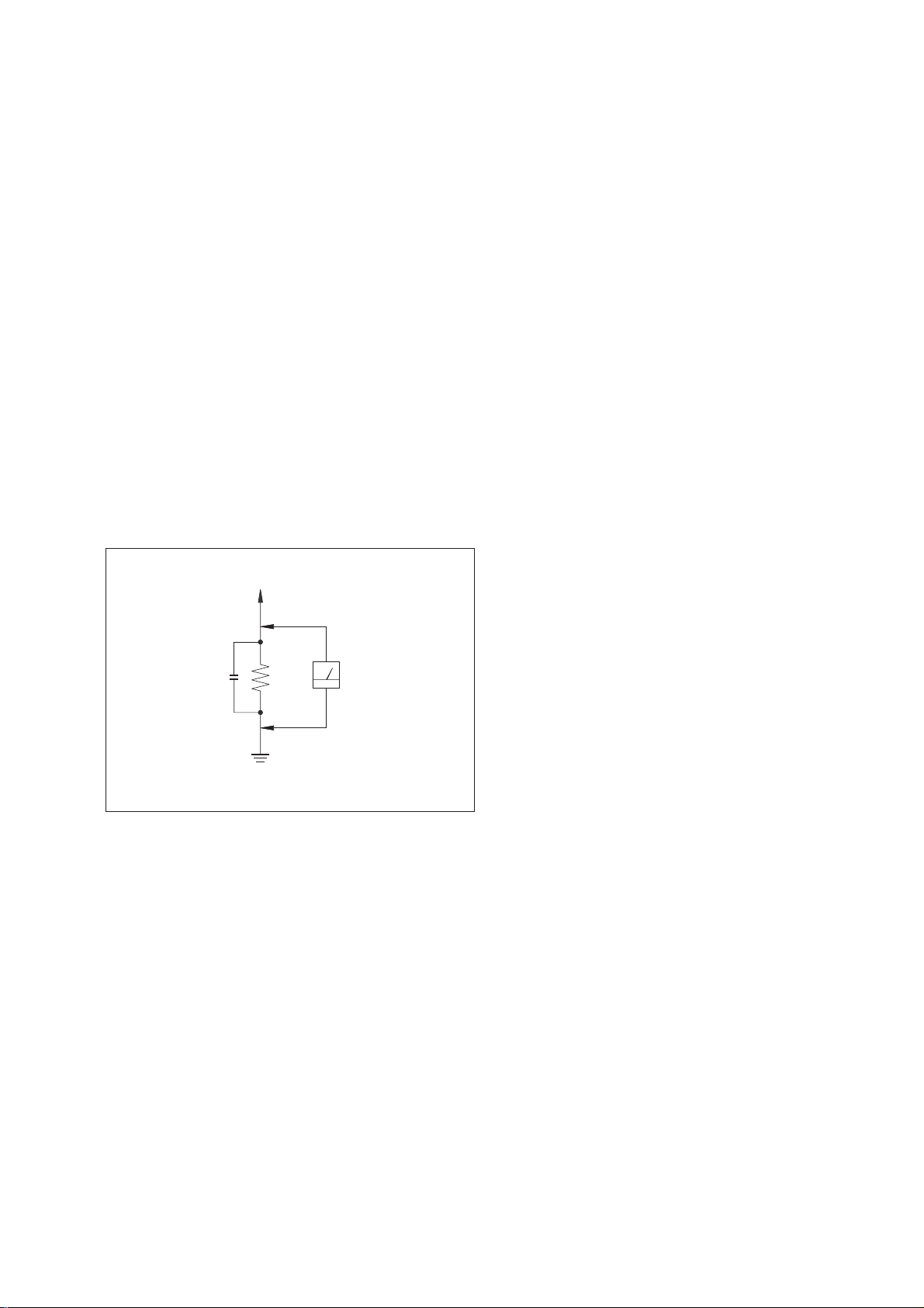
LEAKAGE
The AC leakage from any exposed metal part to earth Ground and
from all exposed metal parts to any exposed metal part having a
return to chassis, must not exceed 0.5 mA (500 microampers).
Leakage current can be measured by any one of three methods.
1. A commercial leakage tester, such as the Simpson 229 or RCA
WT -540A. F ollow the manufactur ers’ instructions to use these
instruments.
2. A battery-operated AC milliammeter. The Data Precision 245
digital multimeter is suitable for this job.
3. Measuring the voltage drop across a resistor by means of a
VOM or battery-operated A C voltmeter . The “limit” indication
is 0.75 V, so analog meters must have an accurate low-v oltage
scale. The Simpson 250 and Sanwa SH-63Trd are e xamples of
a passive VOM that is suitable. Nearly all battery operated
digital multimeters that have a 2V AC range are suitable. (See
Fig. A)
T o Exposed Metal
Parts on Set
AC
0.15
µ
F
Fig. A. Using an A C v oltmeter to check A C leakage.
1.5 k
Ω
Earth Ground
Voltmeter
(0.75 V)
TABLE OF CONTENTS
1. GENERAL ········································································· 4
—FRONT PANEL— ·························································4
—BACK PANEL—····························································5
2. DISASSEMBLY
2-1. Top Cover ··········································································· 6
2-2. Front Panel Assy································································· 6
2-3. Main Board········································································· 7
2-4. Main Section······································································· 7
2-5. CD Mechanism Deck Section ············································ 8
2-6. Tape Mechanism Deck ······················································· 8
2-7. Cassette Door ····································································· 9
2-8. CD Door Assy ···································································· 9
2-9. Base Unit ··········································································10
2-10. Disc T able········································································· 10
3. MECHANICAL ADJUSTMENTS ····························· 11
4. ELECTRICAL ADJUSTMENTS ······························· 11
5. DIAGRAMS
5-1. Circuit Boards Location ··················································· 16
5-2. Block Diagram —Deck Section— ··································· 17
5-3. Block Diagram —Tuner/CD Section— ··························· 19
5-4. Schematic Diagram —Main Section (1/2)— ··················· 21
5-5. Schematic Diagram —Main Section (2/2)—
(US, AUS, MX model) ····················································· 25
5-6. Printed Wiring Board —Main Section—
(US, AUS, MX model) ····················································· 29
5-7. Printed Wiring Board —Main Section—
(AEP, UK, E, SP, MY, AR model)···································· 34
5-8. Schematic Diagram —Main Section (2/2)—
(AEP, UK, E, SP, MY, AR model)···································· 39
5-9. Schematic Diagram —Display Section— ························ 43
5-10. Printed Wiring Board —Display Section— ····················· 47
5-11. Printed Wiring Board —CD Section—···························· 52
5-12. Schematic Diagram —CD Section— ······························· 57
5-13. Schematic Diagram —Power Section— ·························· 60
5-14. Printed Wiring Board —Power Section— ······················· 63
5-15. IC Block Diagrams ··························································· 68
5-16. IC Pin Function Description············································· 71
— 3 —
6. EXPLODED VIEWS
6-1. Top Cover Section ···························································· 73
6-2. CD Door Section ······························································ 74
6-3. Panel Section ····································································75
6-4. Main Section····································································· 76
6-5. Cassette Button Section···················································· 77
6-6. Cassette Mechanism Deck Section··································· 78
6-7. CD Mechanism Deck Section ·········································· 79
6-8. Base Unit Section ····························································· 80
7. ELECTRICAL PARTS LIST ······································ 81
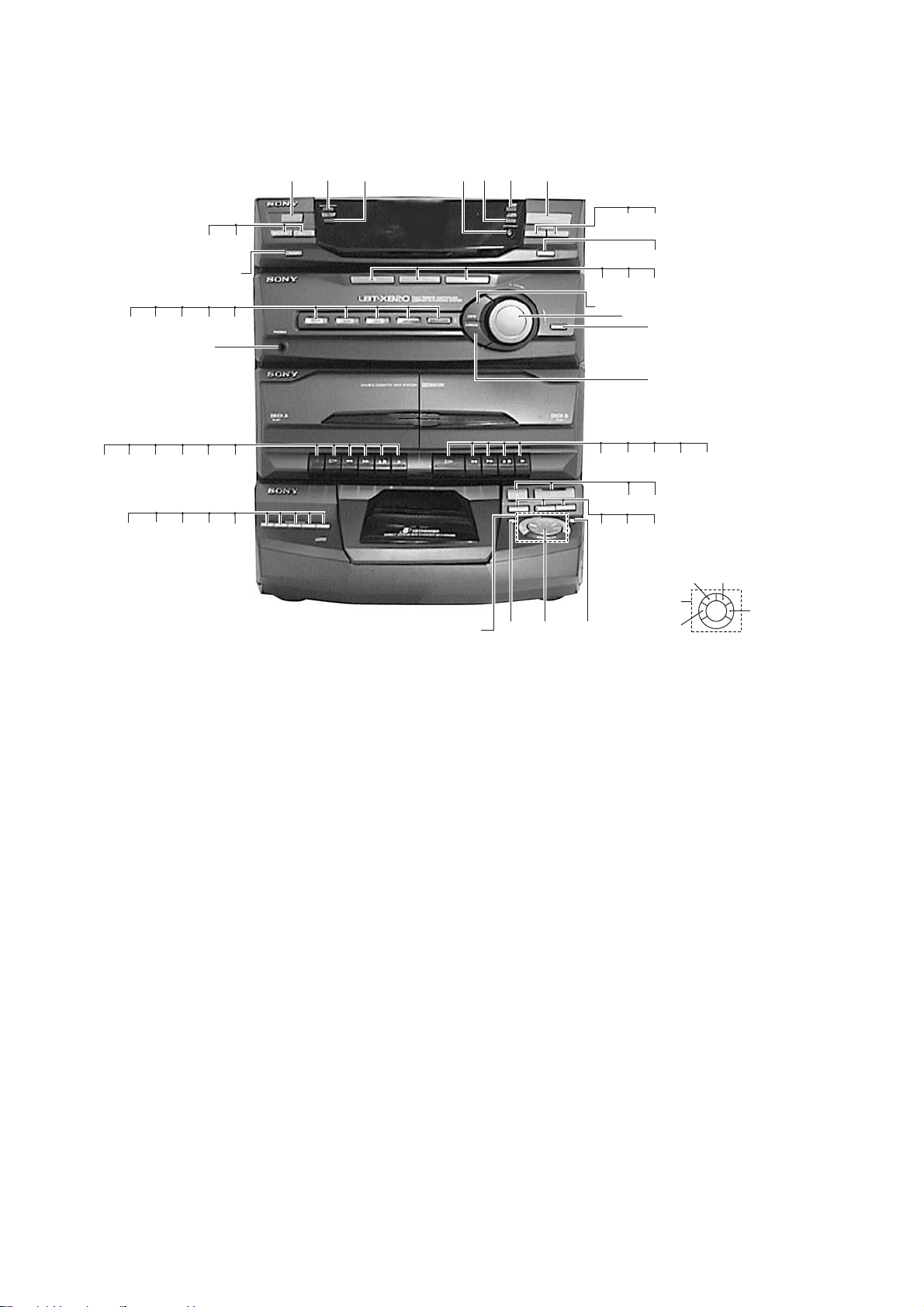
– FRONT PANEL –
SECTION 1
GENERAL
#§
#¶
#¡
$¢
$∞
#•
#ª
#™ #£
$ª
$§$£
$™
$º
#¢
%º
$•
$¶
$¡
#∞
1
2
3467
see
A
5
#º
@ª
@•
!¡
!¢
!•
@∞
89
!º
!™
!£
!∞
!§
!¶
!ª
@º
@¢
@£
@¶
@§
@¡
%¢ %¡
A
%£
@™
%™
1 I/u (POWER) button
2 DISPLA Y/DEMO button
3 SPECTRUM ANALYZER button
4 ENTER/NEXT button
5 TUNER MEMORY button
6 TUNING MODE button
7 TUNER/BAND button
8 TUNING – button
9 TUNING + button
0 STEREO/MONO button
!¡ TAPE button
!™ CD button
!£ PHONO button
!¢ DBFB button
!∞ VOLUME knob
!§ DOLBY NR button
!¶ SURROUND button
!• · button
!ª 0 button
@º ) button
@¡ 6p button
@™ P button
@£ 6 button
@¢ · button
@∞ DISC SKIP button
@§ P button
@¶ p button
@• ) button
@ª ≠ AMS ± button
#º 0 button
#¡ DISC1 button
#™ DISC2 button
#£ DISC3 button
#¢ DISC4 button
#∞ DISC5 button
#§ r button
#¶ · button
#• 0 button
#ª ) button
$º 6p button
$¡ P button
$™ PHONES jack
$£ ROCK button
$¢ POP button
$∞ JAZZ button
$§ SALSA button
$¶ FLAT button
$• SLEEP button
$ª t/CLOCK SET button
%º DAILY1 button
%¡ PLAY MODE button
%™ REPEAT button
%£ EDIT button
%¢ 1/ALL DISC button
— 4 —
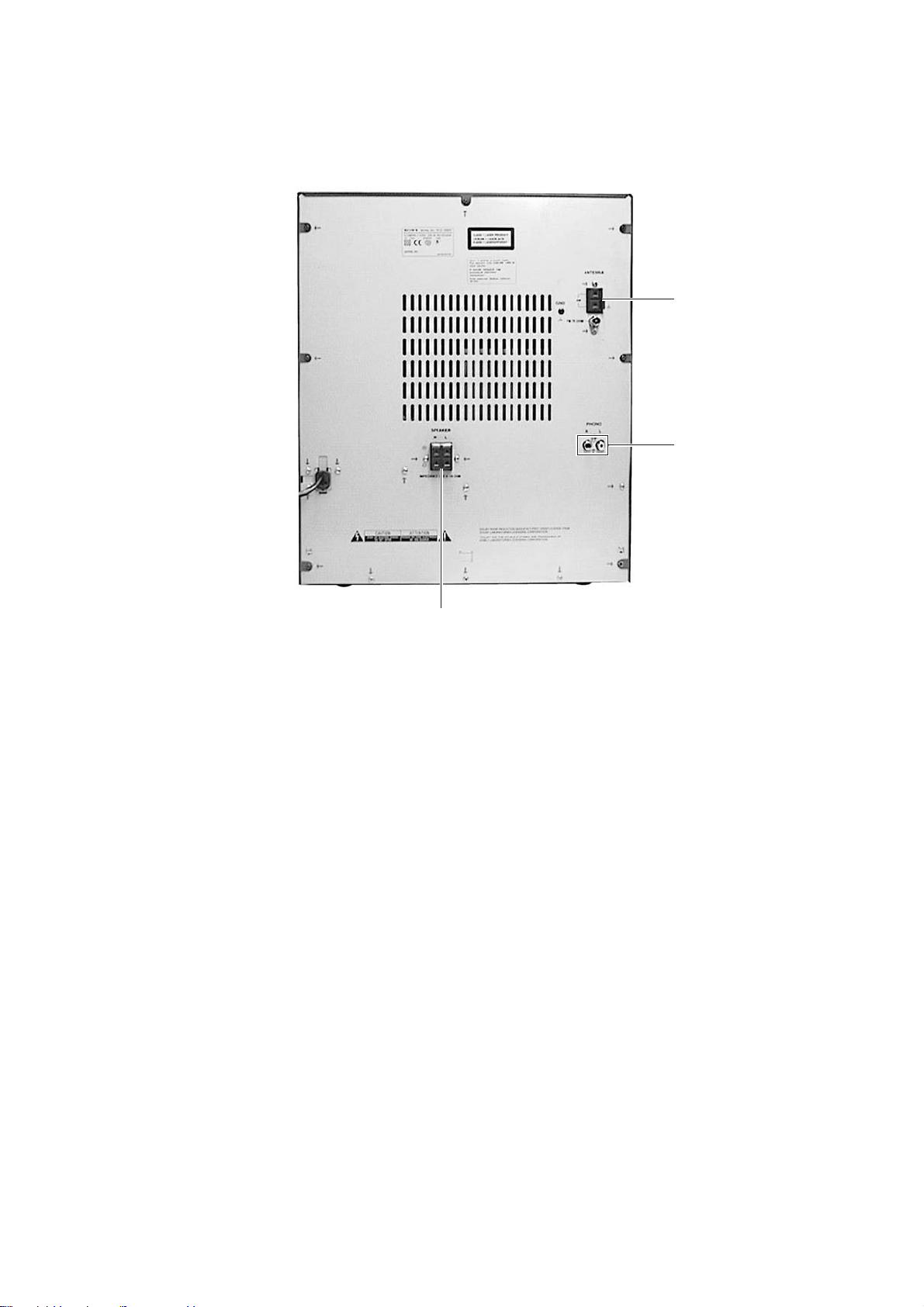
– BACK PANEL –
1
2
1 ANTENNA terminal
2 PHONO jack
3 SPEAKER terminal
3
— 5 —

SECTION 2
DISASSEMBLY
Note : Follow the disassembly procedure in the numerical order given.
2-1. TOP COVER
1
Three screws
3
Top cover
2
Seven screws
1
Three screws
2-2. FRONT PANEL ASSY
3
Front panel assy
1
Screw
2
Four screws
— 6 —
2-3. MAIN BOARD
1
Two screws
2
Three screws
2
Three screws
2
Two screws
1
Three screws
3
Rear panel
7
MAIN board
6
Two screws
5
Two flat wires
4
Connector
2-4. MAIN SECTION
1
Two screws
2
Main section
1
Two screws
— 7 —

2-5. CD MECHANISM DECK SECTION
3
Five screws
(BVTP 3 × 8)
4
CD mechanism
deck section
2
Flat wire and
lead wire
2-6. TAPE MECHANISM DECK
1
Open the clamp.
1
Six screws
2
Tape mechanism deck
— 8 —
2-7. CASSETTE DOOR
3
Door spring
2
Cassette door (L)
2-8. CD DOOR ASSY
1
Cassette door (R)
7
Connector
5
3
Door spring
DOOR SW board
6
Four screws
8
CD door assy
4
Screw
— 9 —
3
Three flat wires
1
Three screws
2
PLAY SW board
2-9. BASE UNIT
t
3
Base unit
1
Yoke bracke
2-10. DISC TABLE
Note:
When the disc table is installed, adjust the positions
of roller cam and mark z as shown in the figure,
then set to the groove of disc table.
A
2
1
Screw
(BVTP 3 × 8)
2
Bracket (BU)
Boss
1
Screw
(BVTP 3 × 8)
3
Step screw
4
Disc table
— 10 —
A

SECTION 3
MECHANICAL ADJUSTMENTS
SECTION 4
ELECTRICAL ADJUSTMENTS
Precaution
1. Clean the following parts with a denatured alcohol-moistened
swab:
record/playback head pinch rollers
erase head rubber belts
capstan idlers
2. Demagnetize the record/playback head with a head
demagnetizer.
3. Do not use a magnetized screwdriver for the adjustments.
4. After the adjustments, apply suitable locking compound to the
parts adjusted.
5. The adjustments should be performed with the rated power
supply voltage unless otherwise noted.
Torque Measurement
Torque
FWD
FWD
back tension
FF/REW
Torque meter
CQ-102C
CQ-102C
CQ-201B
Meter reading
40 to 70 g • cm
(0.56 - 0.97 oz • inch)
1 to 5 g • cm
(0.01 - 0.07 oz • inch)
55 to 140 g • cm
(0.76 - 1.94 oz • inch)
DECK SECTION 0 dB=0.775V
1. Demagnetize the record/playback head with a head
damagnetizer.
2. Do not use a magnetized screwdriver for the adjustments.
3. After the adjustments, apply suitable locking compound to the
parts adjusted.
4. The adjustments should be performed with the rated power
supply voltage unless otherwise noted.
5. The adjustments should be performed in the order given in this
service manual. (As a general rule, playback circuit adjustment
should be completed before performing recording circuit
adjustment.)
6. The adjustments should be performed for both L-CH and RCH.
Tape
P-4-A100
WS-48B
Record/Playback Head Azimuth Adjustment
(Deck A, Deck B)
Note: Perform this adjustments for both decks.
Procedure:
1. Mode : Playback
test tape
P-4-A100
(10kHz, –10dB)
Signal
10 kHz, –10 dB
3 kHz, 0 dB
SPEAKER
terminal (JK703)
Used for
Azimuth Adjustment
Tape Speed Adjustment
level meter
set
+
–
— 11 —

2. Turn the adjustment scre w and check output peaks. If the peaks
do not match for L-CH and R-CH, turn the adjustment screw
so that outputs match within 2 dB of peak.
L-CH
peak
screw
position
R-CH
peak
output
level
within
2dB
L-CH
peak
R-CH
peak
within 2dB
screw
position
4. After the adjustments, apply suitable locking compound to the
parts adjusted.
Adjustment Location:
Remove the cassette lid before adjustment (See page 9)
Adjustment screws
REC/PB head (deck A)
or PB head (deck B)
3. Mode: Playback
test tape
P-4-A100
(10kHz, –10dB)
in phase 45˚ 90˚ 135˚ 180˚
SPEAKER
terminal (JK703)
(L-CH)
L
set
R
SPEAKER
terminal (JK703)
(R-CH)
Waveform of oscilloscope
good
wrong
Tape Speed Adjustment (Deck A)
Procedure:
1. Mode: Playback
test tape
WS-48B
(3kHz, 0dB)
set
SPEAKER
terminal (JK703)
frequency counter
+
–
2. Adjust the SFR809 so that the frequency counter reads 3,000
Hz ± 90Hz.
Adjustment Location: MAIN board (See page 14)
Sample Value of Wow and flutter
W. RMS (JIS) within 0.3%
(test tape: WS-48B)
— 12 —
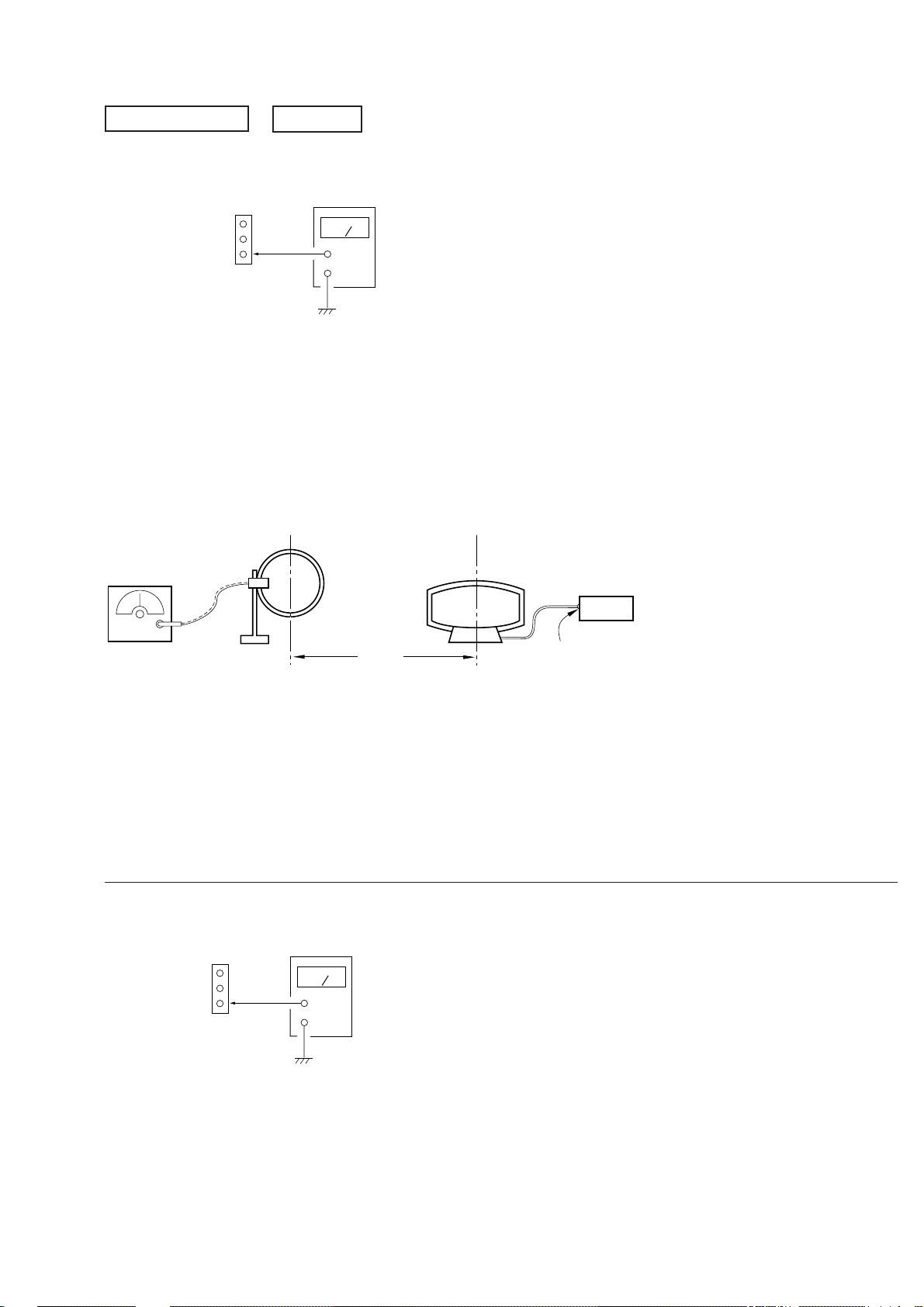
TUNER SECTION 0 dB=1µV
AM Tuning Voltage Adjustment
Main board
TP1
F
G
VT
DC voltmeter
+
–
Procedure:
1. Set the reception frequency of the unit to 530 kHz.
2. Adjust L105 for 1.2 ± 0.05 V reading on the DC voltmeter.
3. Set the reception frequency of the unit to 1,710 kHz.
4. Confirm that the voltage reading on the DC voltmeter is within
8.0 ± 0.5 V.
Adjustment Location: MAIN board (See page 14)
AM Tracking Adjustment
loop antenna
AM RF SSG
loop antenna
(Supplied accessories)
set
30% amplitude
modulation by
400 Hz signal
60 cm
Field strength dB (
µ
V/m) =SSG output level dB (µV/m) –26 dB.
Procedure:
1. Tune the set to 600 kHz.
2. Set the output of AM RF SSG so that the input le vel of the set
will become 60 dB (µV/m).
3. Adjust L104 so that when the waveform on the oscilloscope is
maximum, no noise appears.
4. Tune the set to 1,400 kHz.
FM Tuning Voltage Adjustment (US, Australian, Mexican model)
Main board
TP1
IF
G
VT
DC voltmeter
+
–
Procedure :
1. Set the reception frequency of the unit to 87.5 MHz.
2. Adjust L103 for 1.2 ± 0.05V reading on the DC voltmeter.
3. Set the reception frequency of the unit to 108 MHz.
4. Confirm that the voltage reading on the DC voltmeter is within
7.8 ± 0.5V.
AM ANTENNA
terminal (TM1)
5. Adjust TC102 so that when the waveform on the oscilloscope
is maximum, no noise appears.
• Repeat the procedures in each adjustment several times, and the
tracking adjustment should be finally done by the trimmer
capacitors.
Adjustment Location: MAIN board (See page 14)
Adjustment Location: MAIN board (See page 14)
— 13 —
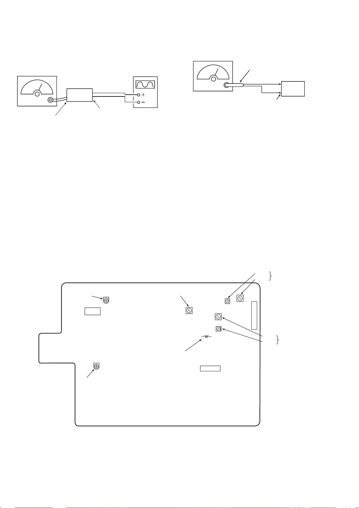
FM Tracking Adjustment
)
(US, Australian, Mexican model)
Procedure:
FM RF SSG
set
SPEAKER terminal (JK703)
FM ANTENNA terminal (JK101)
Carrier frequency : 90 MHz, 106 MHz
Modulation : AUDIO 1kHz, 75kHz deviation (100%)
Output level : 20 dB (at 75 Ω open)
oscilloscope
1. Tune the set to 90 MHz.
2. Adjust L102 so that when the waveform on the oscilloscope is
maximum, no noise appears.
3. Tune the set to 106 MHz.
4. Adjust TC101 so that when the waveform on the oscilloscope
is maximum, no noise appears.
• Repeat the procedures in each adjustment several times, and the
tracking adjustment should be finally done by the trimmer
capacitors.
Adjustment Location: MAIN board
FM Tuned Level Adjustment
FM RF SSG
Ω
coaxial
75
set
Carrier frequency : 98 MHz
Modulation : AUDIO 1 kHz, 75 kHz
Output level : 28 dB (at 75
deviation (100%)
Ω
open)
FM ANTENNA terminal
(JK101)
Procedure:
1. Supply a 28 dB 98 MHz signal from the ANTENN A terminal.
2. Tune the set to 98 MHz.
3. Adjust SFR101 to the point (moment) when the TUNED
indicator will change from going off to going on.
Adjustment Location: MAIN board
Adjustment Location
[MAIN BOARD] — Component side —
SFR101
(FM Tuned Level)
IC103
SFR809
(Tape speed)
L105
(AM Tuning
Voltage)
L103
(FM Tuning
Voltage)
IC301
JK101
TC102
L104
L102
TC101
(AM
Tracking)
(FM
Tracking
— 14 —
CD SECTION
)
Note:
1. CD Block is basically constructed to operate without
adjustment. Therefore, check each item in order given.
2. Use YEDS-18 disc (3-702-101-01) unless otherwise indicated.
3. Use an oscilloscope with more than 10MΩ impedance.
4. Clean the object lens by an applicator with neutral detergent
when the signal level is low than specified value with the
following checks.
5. Adjust the focus bias adjustment when optical block is replaced.
Focus Bias Adjustment
CD DECODER
board
TP02
FEO
VC
Procedure:
1. Connect DC voltmeter to test point TP02 on CD DECODER
board.
2. Turned Power switch on.
3. Put disc (YEDS-18) in and stop.
4. Adjust VR01 so that the DC voltmeter reading is 0 ± 20 mV.
DC voltmeter
+
–
RF Level Check
CD DECODER
board
TP01
RF
VC
oscilloscope
Procedure :
1. Connect oscilloscope to test point TP01 on CD DECODER
board.
2. Turned Power switch on.
3. Put disc (YEDS-18) in and playback.
4. Confirm that oscilloscope waveform is clear and check RF
signal level is correct or not.
Note: Clear RF signal waveform means that the shape “◊” can be
clearly distinguished at the center of the waveform.
VOLT/DIV: 200 mV
TIME/DIV: 500 nS
level: 1.0 Vp-p
+0.3
–0.2
Adjustment Location: CD DECODER board
Adjustment Location: CD DECODER board
Focus Gain Adjustment (VR02)
This gain has a margin, so even if it is slightly off.
There is no problem.
Therefore, do not perform this adjustment.
Please note that it should be fixed to mechanical center position
when you moved and do not know original position.
Adjustment Location
[CD DECODER BOARD] — Component side —
TP01
VR01
(Focus Bias)
IC01
VR02
(Focus Gain
TP02
— 15 —
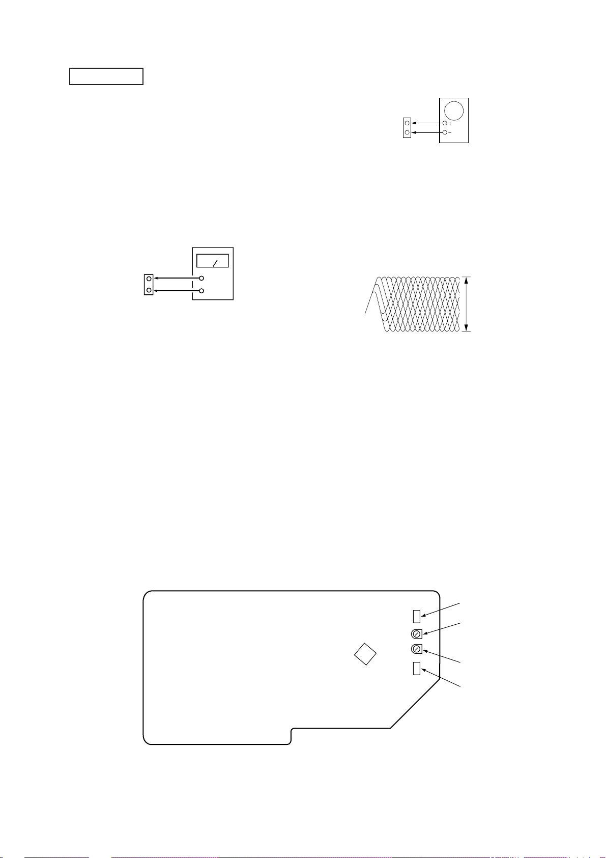
5-1. CIRCUIT BOARDS LOCATION
MAIN board
SECTION 5
DIAGRAMS
AMP board
POWER SELECT board
LED board
DISC board
DOOR SW board
POWER SUPPLY
board
FRONT board
VR board
PLAY SW board
JOG board
R/P SWITCH board
TABLE SENSOR board
MOTOR board
CONNECTOR board
— 16 —
DISC NO LED board
MOTOR (6P)(C) board
CD DECODER board
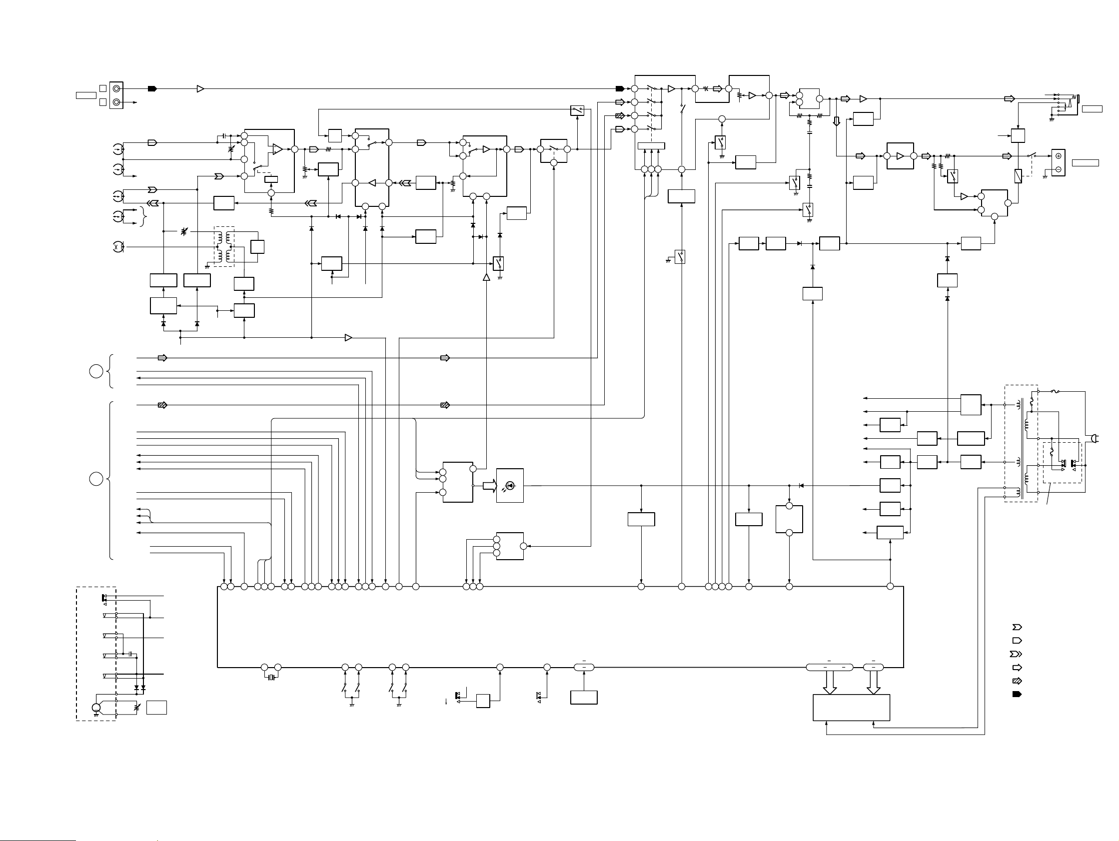
5-2. BLOCK DIAGRAM — DECK SECTION —
PHONO
TAPE B
TAPE A
HRP901
REC/PB
SECTION
SECTION
MECHANISM
BLOCK
SW201
S804
S804
S803
S802
S801
16
HP901
PB
HEAD
HEAD
HE901
ERASE
HEAD
A
TUNER
B
CD
M
JK301
L
R
TU MUTE
TABLE SENSOR
TU L
ST IND
CD L
SCOR
SENS
SQSO
XLAT
SQCK
DATA
COUNT
FOK
CLK
STB
DO
CE
DI
UP SW
R CH
R CHR CH
Q803,805
R CH
PLAY/REC
CONTROL
Q823
PLAY/REC
CONTROL
D803
SFR809
TAPE
SPEED
DRIVE
SFR807
SFR807
Q801
D802
REC +B
REC +B
A MOTOR +B
B PLAY +B
MOTOR +12V
IC402
PLAY/REC
CONTROL
SFR801
BIAS OSC
+12V
L805
BIAS
TRAP
L809
Q818
Q809
78
77
UP SW
TABLE SENSOR
6
5
9
7
Q816,817
BIAS
SWITCH
MUTE
CONT
91
STB
BIAS
OSC
CE
93CE97
EQ AMP
IC801
PB OUT
A/B
CLK
98
CLK
16
12
X601
6MHz
2
SFR803
3
DO
76
28
SO
FOK
COUNT
X217X1
Q803
10
MPX
14
Q807
REC
MUTE
MUTE
13
D805
D804
D801 D806
Q825,826
MUTE
CONT
B PLAY +B A MOTOR +B
Q819
95
97
34
96
75
27
XLAT
DATA
SQCK
SQSO
A
SENS
SCOR
81
VR601
VOLUME
VR UP
REC AMP
MUTE
15 1
89
3
SI
VR DOWN
82
B
PB/REC
AMP
IC802
D807
73
TU MUTE
FM ST IND
11
12
10
74
CD SYNC
FUNCTION TAPE
CD ENCODER A83CD ENCODER B
84
A
B
VR602
CD
ENCODER
BUFFER
CLK
98
ALATCH
Q811
Q813
MUTE
DI
SFR805
2
3
4
SW101
10k
9k
14
16
D808
LED DRIVE
IC602
+5.6V
HCD-G2500/XB20/XB22
SELECTOR
IC301
11
Q602
Q602
9
10
12
CONTROL
RESET
SWITCH
12
DI
RESET
CLK14DI15CE
CLK
16
CE
Q301
DOLBY
AMP
IC803
IC803
11
9
12
5
Q815
PB
MUTE
MUTE
D810
D809
Q820
Q822
LED601-609
16
SPANA
IC603
1
8
26
25
24
SPANA 3
SPANA 2
SPANA 1
Q605,606
SW
SYSTEM CONTROLLER/
MODE
68
S641
DOOR
514
FLD DRIVER
IC601
23
IC302
K 0
89
6
K1 K4
22 19
KEY
MATRIX
S601-624
S601-624
S626-640
LT COM
4
Q307
SURROUND
CONTROL
Q310
7
3 2
SURROUND
8
FLAT
ROCK
8
Q303
5
6
DBFB HIGH
DBFB NORMAL
Q311
MUTE
Q603
MUTE
SWITCH
Q601
Q601
POWER
DOWN DET
2
13
SYSTEM MUTE
1
POWER DOWN
Q604
MUTE
RM601
Q305
HIGH
Q308
NORMAL
3
REMOTE
CONTROL
RECEIVER
2
29
REMOTE
LINE AMP
4
3
D302
D602
IC303
Q402
POWER
MUTE
45
.
D303
47 50
2
Q410
MUTE
DRIVE
P1 P21
+30V
-30V
-12V
-27V
+12V
CD +7.5V
+12V
M +12V
.
52 67
FLD601
FLD DISPLAY
HP AMP
IC401
3
Q407
MUTE
Q709
MUTE
1
G1 G15
30 44
POWER AMP
IC701
3 11
Q401
-12V
REG
Q702
+7.5V
REG
Q409
+5.6V
REG
Q403
FILTER
Q405,406
SITCHING
1
POWER
Q703
-27V
REG
Q701
+12V
REG
Q712
P MUTE
CONT
D719
D714
Q706
Q708
Q711
AC OFF
DET
D701
RECT
D731,732
VOLTAGE
DOUBLER
D705-708
RECT
R CH
Q404
IC702
SP
RELAY
DRIVE
4
AC3.4V
AC3.4V
SP
DET
6
PT301
• RCH is omitted
• Signal Path
RL701
F702
F703
E, SP, MY, AR MODEL
: PB (DECK A)
: PB (DECK B)
: REC (DECK A)
: FM
: CD
+12V
1
2
SW401
JK401
PHONES
JK703
SPEAKER
AC
IN
: PHONO
— 17 — — 18 —
 Loading...