

Page 1
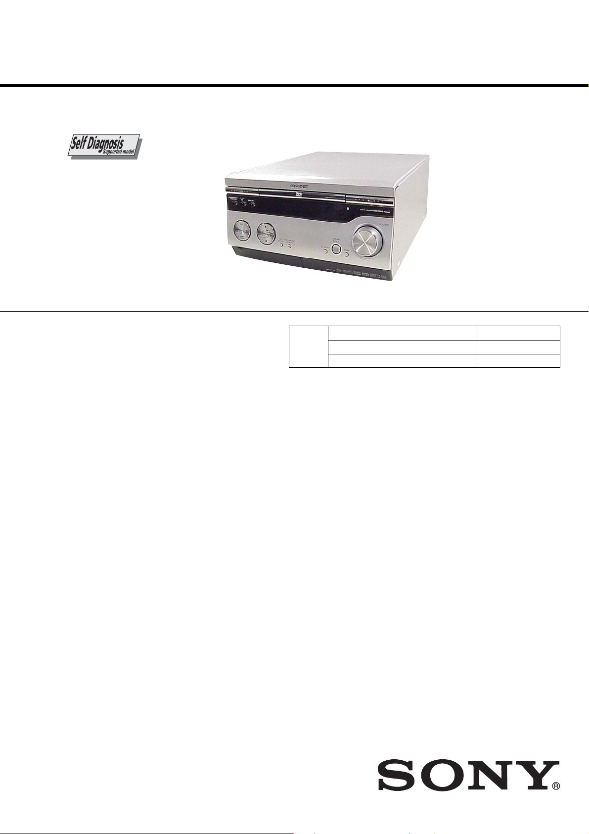
HCD-WZ88D
SERVICE MANUAL
Ver. 1.1 2005.11
HCD-WZ88D is the Tuner, and the CD/DVD
player section in MHC-WZ88D.
This system incorporates with Dolby* Digital and Dolby Pro Logic
(II) adaptive matrix surround decoder and the DTS** Digital
Surround System.
* Manufactured under license from Dolby Laboratories.
“Dolby,” “Pro Logic,” and the double-D symbol are
trademarks of Dolby Laboratories.
** Manufactured under license from Digital Theater Systems, Inc.
“DTS” and “DTS Digital Surround” are trademarks of
Digital Theater Systems, Inc.
DVD
Section
SPECIFICATIONS
E Model
Australian Model
Model Name Using Similar Mechanism NEW
DVD Mechanism Type CDM85-DVBU102
Optical Pick-up Name KHM-310CAA/C2NP
Disc player section
System Compact disc and digital
audio and video system
Laser Semiconductor laser
(DVD: λ = 650 nm,
CD: λ = 790 nm)
Emission duration:
continuous
Frequency response DVD (PCM 48 kHz):
2 Hz – 22 kHz (±1dB)
CD: 2 Hz – 20 kHz
(±0.5 dB)
Video color system format
Latin American models NTSC
Other models NTSC, PAL
Tuner section
FM stereo, FM/AM superheterodyne tun er
FM tuner section
Tuning range 87.5 – 108.0 MHz
Antenna FM lead antenna
Antenna terminals 75 ohms unbalanced
Intermediate frequency 10.7 MHz
AM tuner section
Tuning range
Latin American model: 530 – 1,710 kHz
(with the tuning interval
set at 10 kHz)
531 – 1,710 kHz
(with the tuning interval
set at 9 kHz)
Saudi Arabian model: 531 – 1,602 kHz
(with the tuning interval
set at 9 kHz)
Other models: 531 – 1,602 kHz
(with the tuning interval
set at 9 kHz)
530 – 1,710 kHz
(with the tuning interval
set at 10 kHz)
Antenna AM loop antenna
Antenna terminals External antenna terminal
Intermediate frequency 450 kHz
General
Power requirements
Argentina models: 220 V AC, 50/60 Hz
Australian model: 230 – 240 V AC, 50/60 Hz
Saudi Arabian model: 120 – 127 V, 220 V or
230 – 240 V AC, 50/60 Hz
Adjustable with voltage
selector
Thai model: 220 V AC, 50/60 Hz
Other models: 120 V, 220 V or
230 – 240 V AC, 50/60 Hz
Adjustable with voltage
selector
Power consumption 225 watts
Dimensions (w/h/d)
DVD player/Tuner: Approx. 255 × 134 ×
343 mm
Mass
DVD player/Tuner: Approx. 3.0 kg
Supplied accessories: Remote Commander (1)
Batteries (2)
AM loop antenna (1)
FM lead antenna (1)
Speaker pads (20)
Speaker cords (5)
Video cord (1)
Design and specifications are subject to change
without notice.
9-879-693-02
2005K16-1
© 2005.11
CD/DVD PLAYER TUNER
Sony Corporation
Home Audio Division
Published by Sony Engineering Corporation
Page 2

HCD-WZ88D
Notes on chip component replacement
• Never reuse a disconnected chip component.
• Notice that the minus side of a tantalum capacitor may be
damaged by heat.
Flexible Circuit Board Repairing
• Keep the temperature of the soldering iron around 270 °C
during repairing.
• Do not touch the soldering iron on the same conductor of the
circuit board (within 3 times).
• Be careful not to apply force on the conductor when soldering
or unsoldering.
UNLEADED SOLDER
Boards requiring use of unleaded solder are printed with the leadfree mark (LF) indicating the solder contains no lead.
(Caution: Some printed circuit boards may not come printed with
the lead free mark due to their particular size)
: LEAD FREE MARK
Unleaded solder has the following characteristics.
• Unleaded solder melts at a temperature about 40 °C higher
than ordinary solder.
Ordinary soldering irons can be used but the iron tip has to be
applied to the solder joint for a slightly longer time.
Soldering irons using a temperature regulator should be set to
about 350 °C.
Caution: The printed pattern (copper foil) may peel away if
the heated tip is applied for too long, so be careful!
• Strong viscosity
Unleaded solder is more viscou-s (sticky, less prone to flow)
than ordinary solder so use caution not to let solder bridges
occur such as on IC pins, etc.
• Usable with ordinary solder
It is best to use only unleaded solder but unleaded solder may
also be added to ordinary solder.
SAFETY-RELATED COMPONENT WARNING!!
COMPONENTS IDENTIFIED BY MARK 0 OR DOTTED LINE
WITH MARK 0 ON THE SCHEMATIC DIAGRAMS AND IN
THE PARTS LIST ARE CRITICAL TO SAFE OPERATION.
REPLACE THESE COMPONENTS WITH SONY PARTS WHOSE
PART NUMBERS APPEAR AS SHOWN IN THIS MANUAL OR
IN SUPPLEMENTS PUBLISHED BY SONY.
TABLE OF CONTENTS
1. SERVICING NOTES ................................................ 3
2. GENERAL ................................................................... 6
3. DISASSEMBLY
3-2. Case ................................................................................. 10
3-3. Front Panel Assy.............................................................. 10
3-4. VR Board, FL Board, FUNCTION SW Board ............... 11
3-5. 4CH-VOL Board, VIDEO Board .................................... 11
3-6. MAIN Board, REGULATOR Board, MIC Board ........... 12
3-7. DVD Mechanism (CDM85-DVBU102).......................... 12
3-8. DMB10 Board ................................................................. 13
3-9 Tray.................................................................................. 13
3-10. MS-203 Board ................................................................. 14
3-11. Base Unit ......................................................................... 15
3-12 Optical Pick-up (KHM-310CAA/C2NP) ........................ 15
4. TEST MODE ............................................................... 16
5. DIAGRAMS
5-1. Block Diagrams – RF/SERVO Section – ....................... 22
– VIDEO Section –.......................................................... 23
– AUDIO Section – .......................................................... 24
– MAIN Section – ........................................................... 25
5-2. Printed Wiring Board – DMB10 Section (Side A) –....... 26
5-3. Printed Wiring Board – DMB10 Section (Side B) – ....... 27
5-4. Schematic Diagram – DMB10 Section (1/4) – .............. 28
5-5. Schematic Diagram – DMB10 Section (2/4) – .............. 29
5-6. Schematic Diagram – DMB10 Section (3/4) – .............. 30
5-7. Schematic Diagram – DMB10 Section (4/4) – .............. 31
5-8. Printed Wiring Board – MAIN Section – ........................ 32
5-9. Schematic Diagram – MAIN Section (1/2) – ................. 33
5-10. Schematic Diagram – MAIN Section (2/2) – ................. 34
5-11. Printed Wiring Boards – FL/FUNCTION SW Section – 35
5-12. Schematic Diagram – FL/FUNCTION SW Section – .. 36
5-13. Printed Wiring Board – REGULATOR Section – ........... 37
5-14. Schematic Diagram – REGULATOR Section –............. 38
5-15. Printed Wiring Board – 4-CH-VOL Section – ................ 39
5-16. Schematic Diagram – 4-CH-VOL Section – .................. 40
5-17. Printed Wiring Boards
– VIDEO/MIC/VR/MS-203 Section – ............................ 41
5-18. Schematic Diagram
– VIDEO/MIC/VR/MS-203 Section – ............................ 42
6. EXPLODED VIEWS
6-1. Front Panel Section ......................................................... 54
6-2. Chassis Section................................................................ 55
6-3. Dvd Mechanism Section (CDM85B-DVBU102)............ 56
7. ELECTRICAL PARTS LIST .................................. 58
2
Page 3
SECTION 1
SERVICING NOTES
HCD-WZ88D
NOTES ON HANDLING THE OPTICAL PICK-UP BLOCK
OR BASE UNIT
The laser diode in the optical pick-up block may suffer electrostatic
break-down because of the potential difference generated by the
charged electrostatic load, etc. on clothing and the human body.
During repair, pay attention to electrostatic break-down and also
use the procedure in the printed matter which is included in the
repair parts.
The flexible board is easily damaged and should be handled with
care.
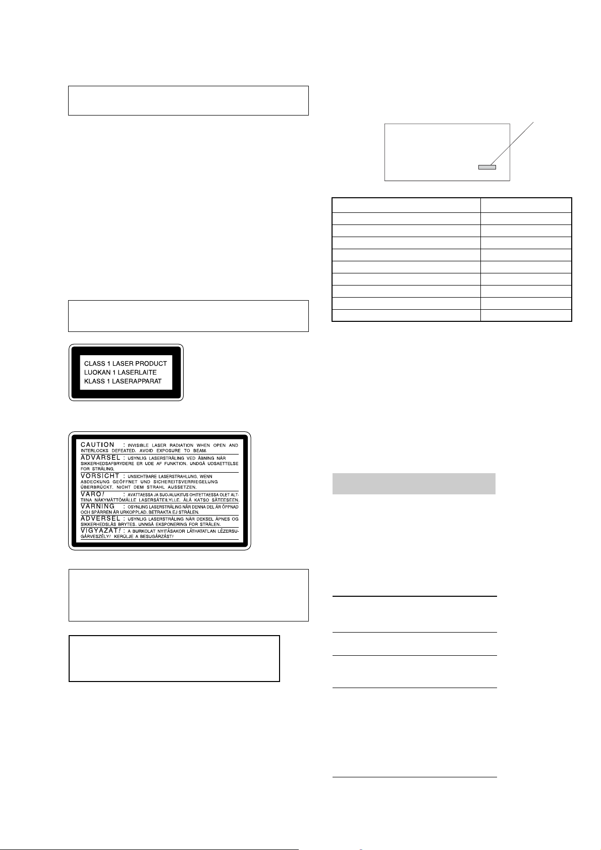
NOTES ON LASER DIODE EMISSION CHECK
The laser beam on this model is concentrated so as to be focused on
the disc reflective surface by the objective lens in the optical pickup block. Therefore, when checking the laser diode emission,
observe from more than 30 cm away from the objective lens.
Laser component in this product is capable of emitting radiation
exceeding the limit for Class 1.
This appliance is classified as
a CLASS 1 LASER product.
The CLASS 1 LASER
PRODUCT MARKING is
located on the rear exterior.
The following caution label is located inside the apparatus.
MODEL IDENTIFICATION
– Rear Panel –
PARTS No.
Model Part No.
SP model 2-580-702-0[]
E12, E13 models 2-580-702-1[]
E15, E3 models 2-580-702-3[]
PL model 2-580-702-4[]
EA model 2-580-702-5[]
AUS model 2-580-702-6[]
TH model 2-580-702-7[]
E51 model 2-580-702-8[]
AR model 2-580-702-9[]
•Abbreviation
AR : Argentine model.
AUS: Australian model.
E3 : 240 V AC area in E model.
E12 : 220-240 V AC area in E model.
E13 : 220-230 V AC area in E model.
E15 : 220-240 V AC area in E model.
E51 : Chilean and peruvian models.
EA : Saudi Arabia model.
PL : Phillippines model.
SP : Singapore and Malaysia models.
TH : Thai model.
CAUTION
Use of controls or adjustments or performance of procedures
other than those specified herein may result in hazardous radiation
exposure.
Note:
HCD-WZ88D does not operate independently.
DXA-WZ88D is required to operate this.
In this case of a service, please connect DXA-WZ88D.
Note on DMB10 board replacement
New part of EEP ROM (IC103) on the DMB10 board cannot be
used. Therefore, if the mounted DMB10 board (A-1122-695-A,
etc. ) is replaced, exchange new EEP ROM (IC103) with that used
before the replacement.
Self-diagnosis function
(When letters/numbers appear in the
display)
When the self-diagnosis function is activated to
prevent the system from malfunctioning, a
5-character service number (e.g. C 13 50) with a
combination of a letter and 4 digits appears in
the on-screen display and the front panel
display. In this case, check the following table.
First 3
characters of
the service
number
C 13 The disc is dirty.
C 31 The disc is not inserted correctly.
E XX
(XX is a number)
Cause and corrective action
t Clea n the disc with a soft cloth
t Restart the system, then
re-insert the disc correctly.
To prevent a malfunction, the
system has performed the selfdiagnosis function.
t Contact your nearest Sony
dealer or local authorized
Sony service facility and give
the 5-character service
number.
Example: E 61 10
3
Page 4
HCD-WZ88D
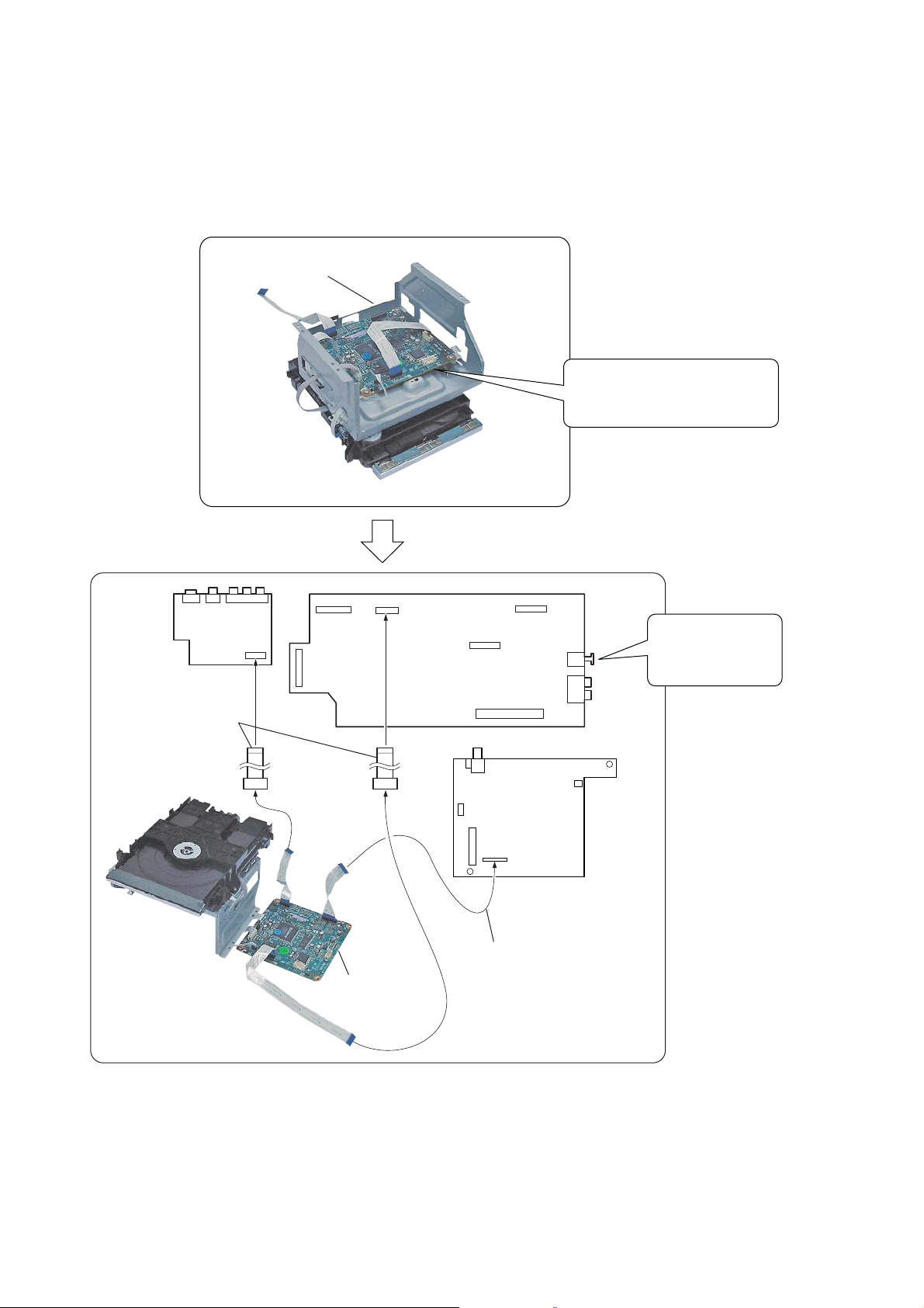
• DMB10 board service position
DMB10 board
Remove the DMB10 board once.
Then create the service position.
VIDEO BOARD
Extension cable :
J-2501-102-A
(1mm / 13pin / L300)
CN801
CN101
MAIN BOARD
DMB10 board
In such a case, the
extension cables
became necessary.
4CH-VOL BOARD
CN303
Extension cable :
J-2501-244-A
(1mm / 21pin / L300)
4
Page 5
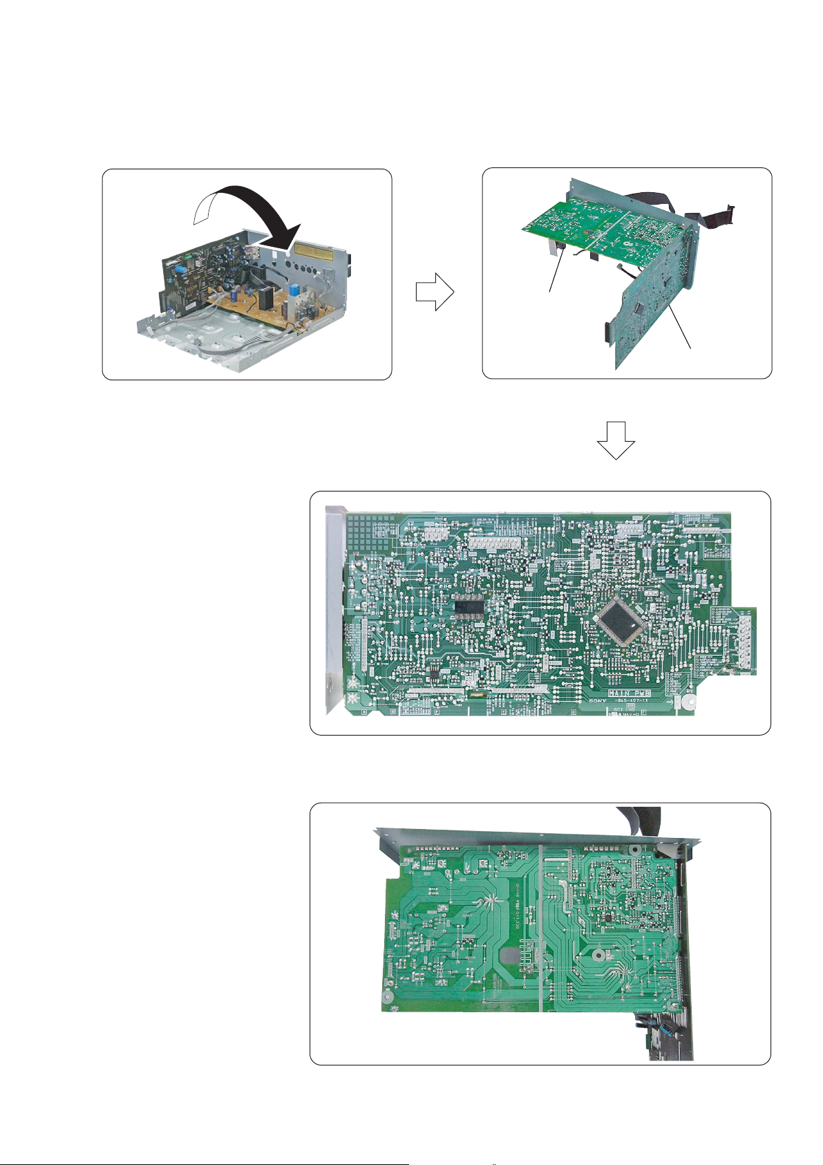
• REGULATOR board service position
REGULATOR board
HCD-WZ88D
MAIN
board
MAIN BOARD
REGULATOR BOARD
5
Page 6
HCD-WZ88D
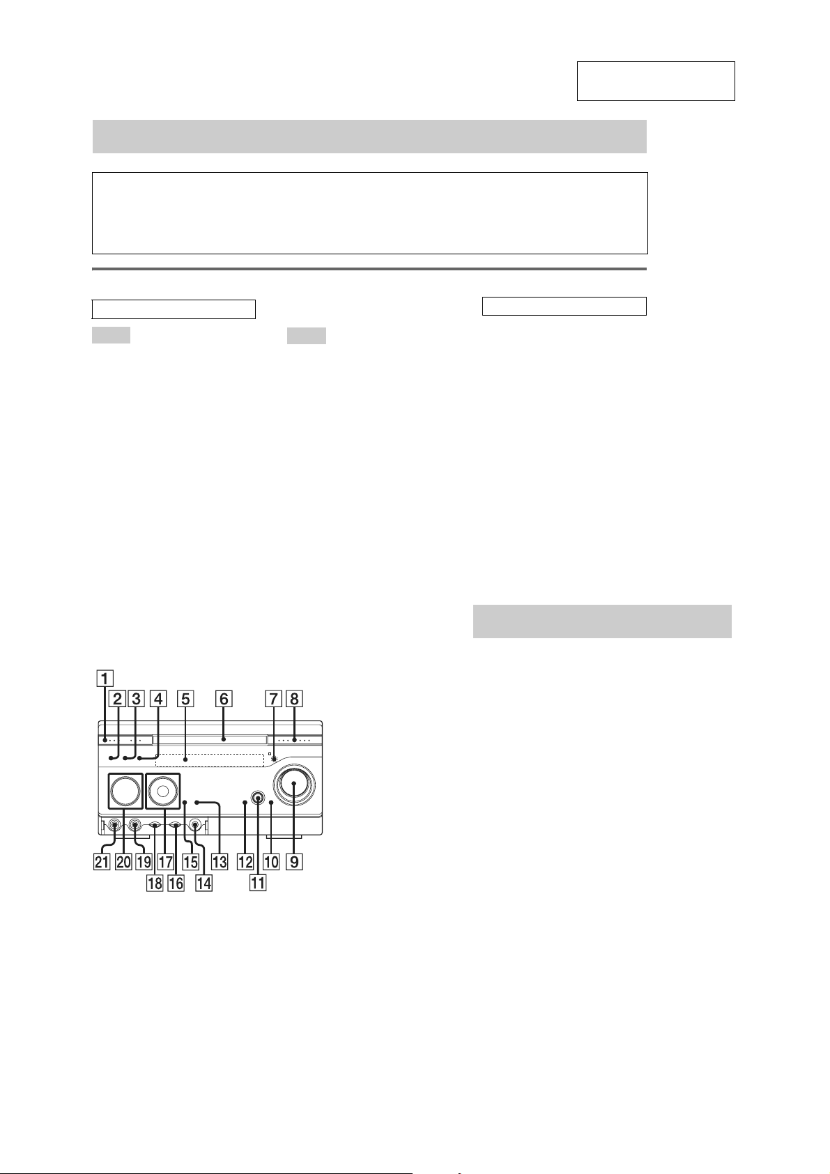
Illustrati
List of button locations and reference pages
SECTION 2
GENERAL
This section is extracted
from instruction manual.
How to use this page
Use these pages to find the location of buttons and
other parts of the unit and the remote that are
mentioned in the text.
Main unit
ALPHABETICAL ORDER
A – L
CD SYNC qg (62, 63, 89)
DIRECTION 2 (61, 63, 71, 75)
Disc tray 6 (15, 18, 30, 31, 33,
37)
DISPLAY 4 (76)
Display window 5 (11)
DSGX q; (64)
DVD
w; (14, 17, 19, 62, 63, 67,
87)
ECHO LEVEL qh (67, 68)
EQ SELECT qs (66, 67)
IR (receptor) 7 (85)
DVD player/Tuner
M – Z
MIC 1 m wa (67, 71, 84)
MIC 2 m ql (67, 71, 84)
MIC LEVEL
PHONES (headphone jack) qf
(84)
PRESET +/– qj (58)
PROGRESSIVE 2 (10, 17, 53,
81, 87)
REC PAUSE/START qd (62, 63,
71)
SA-CD/CD 3 (26, 62)
SOUND FIELD qa (65)
TAPE A/B
TUNER/BAND
63)
VIDEO/SAT
VOLUME 9 (56, 57, 73, 84)
w; (61, 64, 71, 72, 75)
TAPE A/B w; (61, 64, 71, 72, 75)
Name of button/part Reference page
qk (67, 68, 71, 84)
w; (58, 59, 60,
w; (63, 81)
on number
r
RR
BUTTON DESCRIPTIONS
?/1 (power) 1 (11, 59, 81, 89)
X (pause) qj (11)
hH (play) qj (19–21, 27, 30,
33, 36–39, 49, 52, 61–64, 72,
75, 84, 86)
x (stop) qj (59, 62–64, 71, 72,
89)
M> (fast forward/go
forward) qj (19, 27, 30, 31, 38,
61, 62, 64–67)
.m (rewind/go backuard)
qj (19, 27, 30, 31, 38, 61, 62,
64–67)
Z 8 (15, 18, 86)
Setting the clock
1
Press ?/1 to turn on the system.
2
Press TIMER MENU.
The hour indication flashes in the display.
3
Press V or v repeatedly to set the
hour.
4
Press ENTER.
The minute indication flashes in the
display.
5
Press V or v repeatedly to set the
minute.
6
Press ENTER.
The clock starts functioning.
To adjust the clock
1
Press TIMER MENU.
2
Press V or v repeatedly to select “CLOCK
SET?”, then press ENTER.
The hour indication flashes in the display.
3
Do the same procedure as steps 3 to 6
above.
Notes
The clock s ettings are canceled w hen you d isconnect
the power cord or if a power failure occurs.
You cannot set the clock in Power Saving Mode
6
Page 7
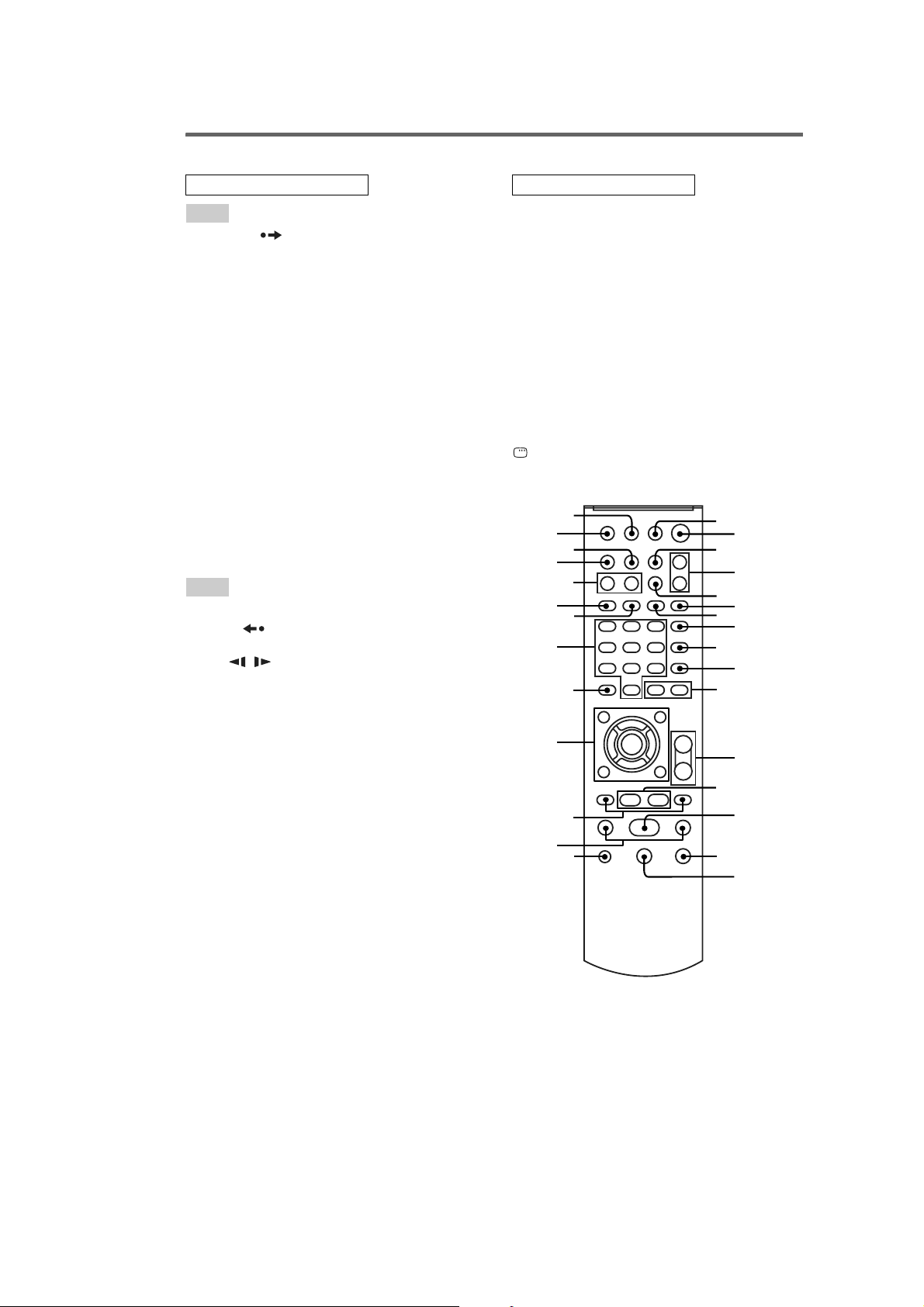
Remote control
HCD-WZ88D
ALPHABETICAL ORDER
A – P
ADVANCE qj (19)
ALBUM +/– ql (16, 19)
ANGLE w; (45)
AUDIO ws (43, 44, 82)
CLEAR 9 (16, 22, 24, 41, 55)
DISC SKIP wj
DISPLAY 4 (76)
ENTER q; (13–15, 19, 21–27, 31–35, 37, 41, 42,
46–51, 55, 56–60, 68–71, 73–75, 89)
FM MODE wd (60, 88)
FUNCTION +/– wh (14, 17, 19, 58, 60, 61, 67, 75, 87)
KARAOKE MODE 6 (68, 82, 87)
KARAOKE PON 7 (68)
KEY CONTROL #/2 5 (69)
MENU 0 (25, 30–33, 37, 58, 59)
Numeric Buttons 8
60)
PICTURE NAVI wf (31, 33, 42)
PRESET –/+ qa (58–60)
R – Z
REPEAT wd (24)
REPLAY qj (19)
SLEEP 2 (16, 73)
SLOW / qs (39)
SOUND FIELD wg (65, 66, 82)
STEP c/C qj (39)
SUBTITLE wa (45)
THEATRE SYNC wl (16)
TIMER MENU 1 (13, 73, 74, 75)
TIME/TEXT 3 (76, 77, 78)
TOP MENU 0 (25)
TUNING +/– qs (58, 60)
TV qd (11)
TV CH +/– qa (11)
TV/VIDEO 2 (11)
TV VOL +/– qk
TV &/1 wk (11)
VOLUME +/– qk
-/-- 9 (11)
10/0 8
1)
2)
(11, 16, 19, 25, 27, 41, 47–51,
2)
(11)
2)
(56, 57, 73, 84)
SYMBOLS
?/1 (power) wk (11, 13, 14, 74, 75, 84)
x (stop) qg (19, 20, 27, 30–33, 37, 46, 59, 61, 75, 86)
X (pause) qf (19, 61)
H (play) qh
61, 62, 75, 84, 86)
. (go backward) qa (19, 27, 30, 31, 38, 62,
64)
> (go forward) qa (16, 19, 27, 30, 31, 38, 62,
64)
m (rewind) qs (38, 61)
M (fast forward) qs (38, 61)
V/v/B/b
40–42, 46–51, 56, 57, 65, 68–71, 73–75, 89)
O RETURN 0 (27, 31, 37, 42)
DISPLAY 0 (15, 21–26, 33, 34, 40–42, 46,
48, 50, 56, 68–71, 79, 89, 97)
2)
(19–21, 27, 30, 33, 36–39, 49, 52,
0 (13–15, 21–23, 25, 26, 30–35, 37,
1
2
3
4
5
6
7
8
wl
wj
wg
wd
wa
wk
wh
wf
ws
w;
9
ql
q;
qk
qj
qh
qg
qs
qa
qd
qf
1)
This button is not available for this model.
2)
The numeric button 5, TV VOL +, VOLUME + and
H buttons have a tactile dot. Use t he tactile dot as
a reference when operating the system.
7
Page 8
HCD-WZ88D
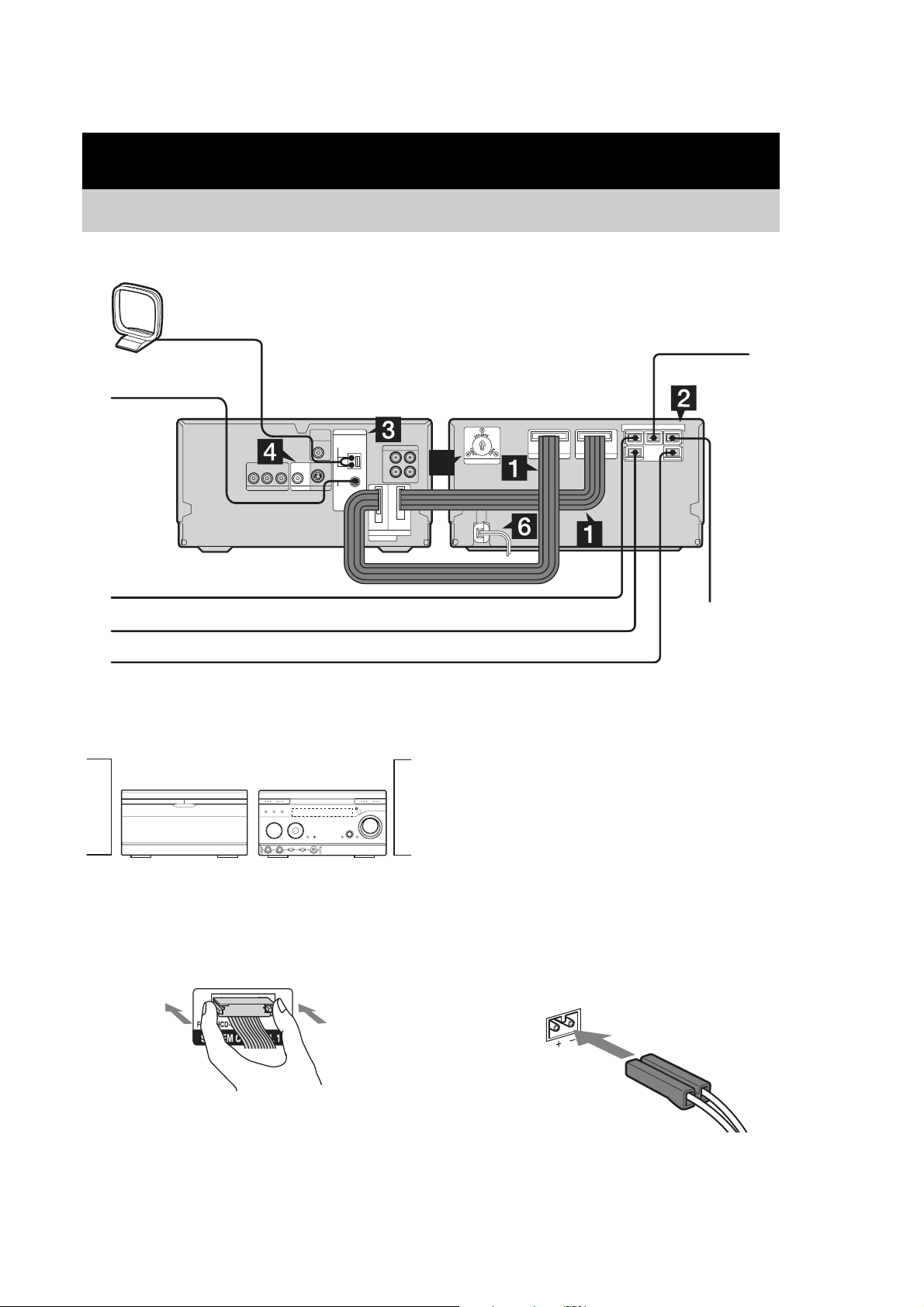
Getting Started
Hooking up the system
Do the following procedures 1 to 7 to hook up your system using the supplied cords and accesso ries.
AM loop antenna
FM lead antenna
To front speaker (right)
To surround speaker (right)
To surround speaker (left)
[HCD-WZ88D] [DXA-WZ88D]
DVD player/Tuner Amplifier/Tape deck
Preparation
Place the components as shown below.
Amplifier/
Tape deck
DVD player/
Tuner
To center
speaker
5
To front speaker
(left)
Note
The system control cables are used to send audio and
electrical signals between the components for
interlinked operation.
Be sure to insert the connector horizontally until it
clicks into place. Otherwise the system will no t operate
correctly.
1 Connect the system control cables
from the DVD player/Tuner component
to the appropriate (same numbered)
SYSTEM CONTROL connectors on the
Amplifier/Tape deck component.
8
2 Connect the speakers.
Be sure to match the appropriate speaker
cords from the speaker terminals to the
corresponding SPEAKER terminals on the
Amplifier/Tape deck component as shown
below.
Amplifier/Tape deck
Page 9
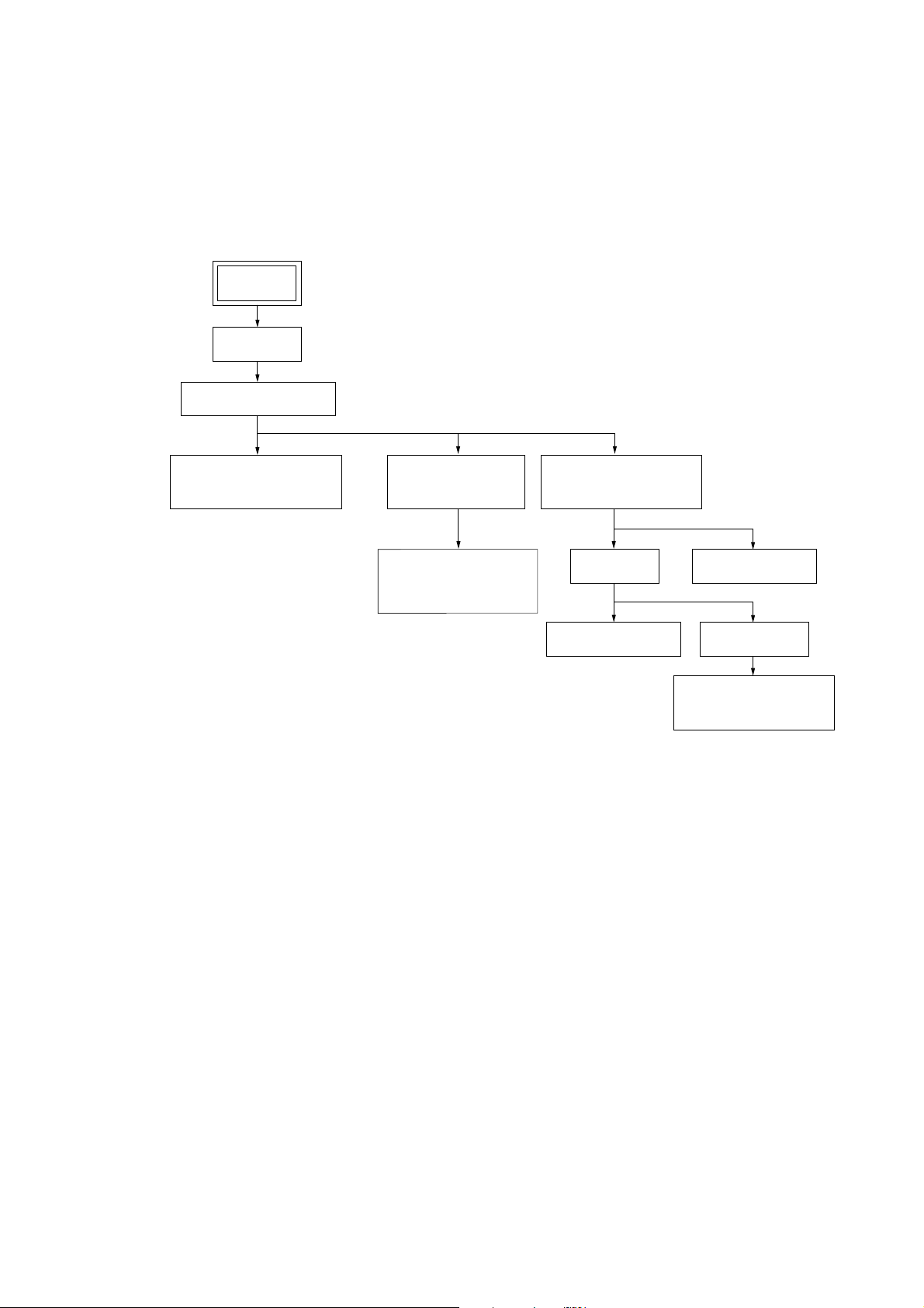
3-1. DISASSEMBLY FLOW
•This set can be disassembled in the order shown below.
SET
3-2.CASE
(Page 10)
3-3.FRONT PANEL ASSY
(Page 10)
3-4.
VR BOARD, FL BOARD,
FUNCTION SW BOARD
(Page 11) (Page 11) (Page 12)
3-5.4CH-VOL BOARD,
SECTION 3
DISASSEMBLY
VIDEO BOARD
(CDM85-DVBU102)
HCD-WZ88D
3-7.DVD MECHANISM
3-6.MAIN BOARD,
REGULATOR BOARD,
MIC BOARD
(Page 12)
3-9.TRAY
(Page 13) (Page 13)
3-10.MS-203 BOARD 3-11.BASE UNIT
(Page 14) (Page 15)
3-8.DMB10 BOARD
3-12.OPTICAL PICK-UP
(KHM-310CAA/C2NP)
(Page 15)
9
Page 10
HCD-WZ88D
Note: Follow the disassembly procedure in the numerical order given.
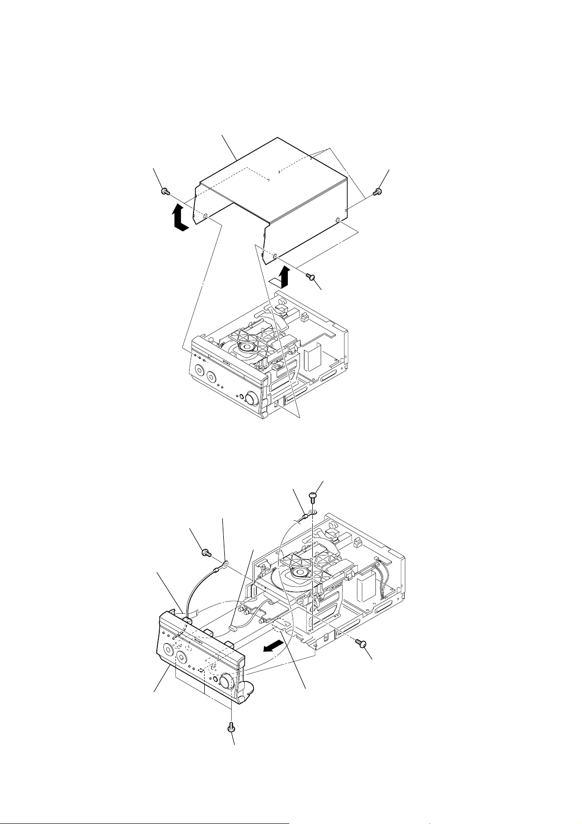
3-2. CASE
4
case
3
two screws
(case 3 TP2)
2
two screws
(case 3 TP2)
1
three screws
(+BVTP 3
×
8)
3-3. FRONT PANEL ASSY
5
wire (flat type)
(23 core) (CN109)
0
front panel
section
2
screw
(+BVTP 3 × 8)
3
earth wire
4
connector
(CN109)
9
7
earth wire
7
6
claw
screw
(+BV 3)
1
screw
(+BVTP 3 × 8)
10
8
three screws
(+BV 3 × 6)
Page 11
3-4. VR BOARD, FL BOARD, FUNCTION SW BOARD
qf
two screws
(+BVTP 2.6 × 8)
7
bracket
(HOLDER-L)
qj
nine screws
(+BVTP 2.6 × 8)
6
screw
(2.6 × 10)
qa
bracket (FL)
0
screw
(2.6 × 10)
9
bracket
(HOLDER-R)
5
knob (MIC)
3
8
screw
qd
bracket (FL)
HCD-WZ88D
two screws
(+BVTP 2.6 × 8)
4
VR board
qg
two screws
(+BVTP 2.6 × 8)
qs
screw
(2.6 × 10)
1
knob (vol)
2
nut
3-5. 4CH-VOL BOARD, VIDEO BOARD
1
9
connector
(CN304)
6
wire (flat type)
(19 core)
wire (flat type)
(23 core)
7
two screws
(+BVTP 3 × 8)
8
4CH-VOL board
2
wire (flat type)
(9 core)
5
(CN302)
cord
qk
qd
(CN107)
connector
qh
FL board
FUNCTION SW board
cord
connector
3
six screws
(+BVTP 3
×
8)
4
two screws
(+BVTP 3 × 8)
0
connector
(CN800)
qs
qa
wire (flat type)
(13 core)
qf
cord
(CN503,CN504)
VIDEO
board
connector
qg
back panel
11
Page 12
HCD-WZ88D
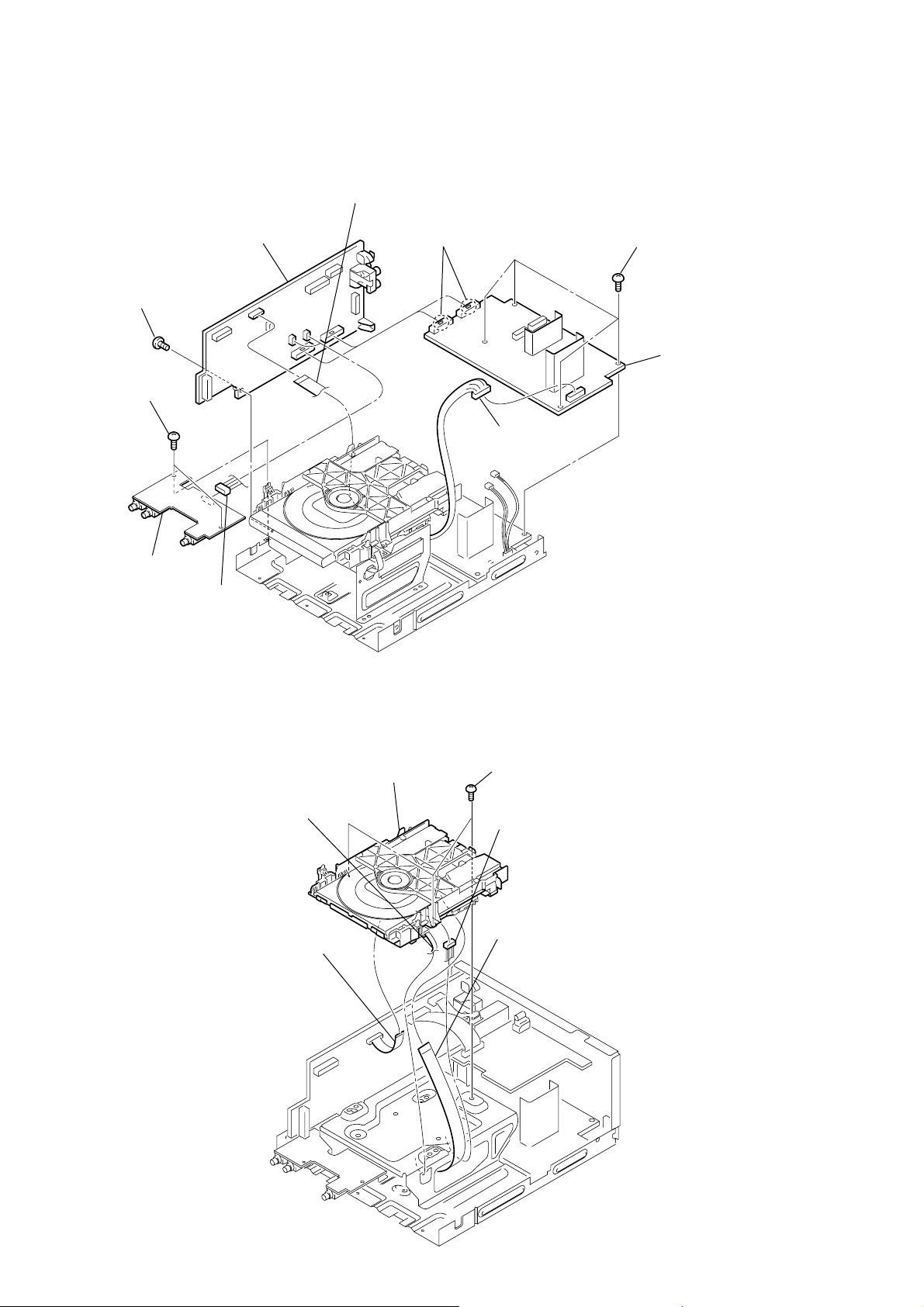
3-6. MAIN BOARD, REGULATOR BOARD, MIC BOARD
1
wire (flat type)
(12 core) (CN101)
5
2
screw
(+BVTP 3
8
two
(+BVTP 3
screws
MAIN board
×
8)
×
8)
4
two claws
6
connector
(CN506)
3
four screws
(+BVTP 3
7
REGULATOR board
×
8)
0
MIC board
9
connector
(CN701)
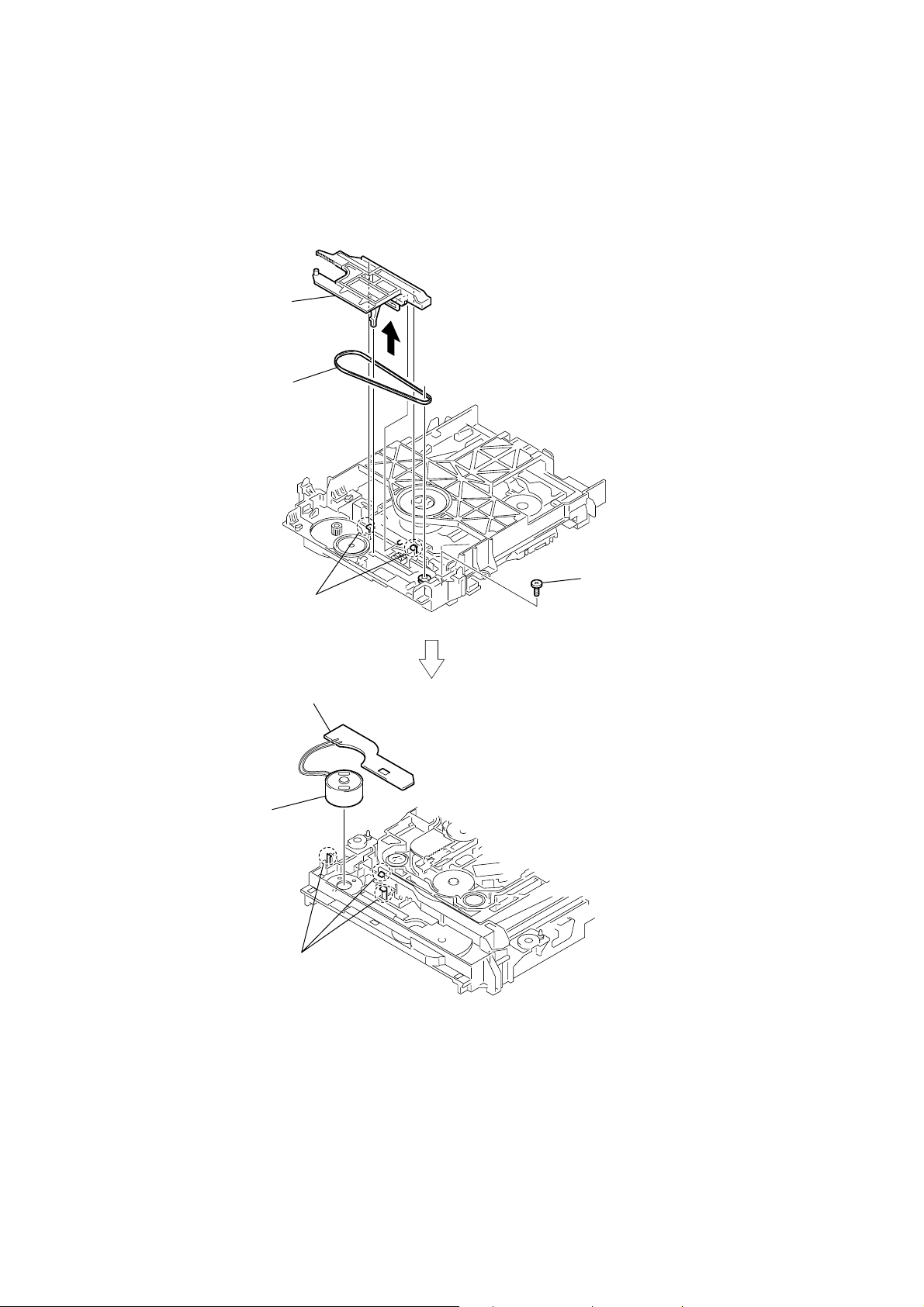
3-7. DVD MECHANISM (CDM85-DVBU102)
6
DVD mechanism
(CDM85-DVBU102)
1
wire (flat type)
(6 core) (CN202)
5
wire (flat type)
(13 core) (CN106)
2
three screws
(+BVTP 3 × 8)
3
connector
(CN201)
4
wire (flat type)
(24 core) (CN101)
12
Page 13
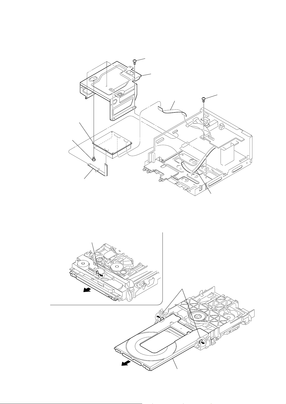
3-8. DMB10 BOARD
8
DMB10 board
7
four screws
(+BVTP 3
HCD-WZ88D
2
four screws (+BV)
6
bracket (CDM)
3
wire (flat type)
(20 core) (CN302)
×
8)
1
screw
(+BVTP 3
×
8)
3-9 TRAY
1
5
wire (flat type)
(13 core) (CN106)
Move the Chuck cam
in the direction of the arrow.
2
bottom side
two claws
3
4
wire (flat type)
(12 core) (CN301)
4
5
tray
13
Page 14
HCD-WZ88D
3-10. MS-203 BOARD
2
chuck cam
3
belt
6
DC motor
1
two claws
7
MS-203 board
5
three claws
4
screw
(M 1.7
×
2.5)
14
Page 15
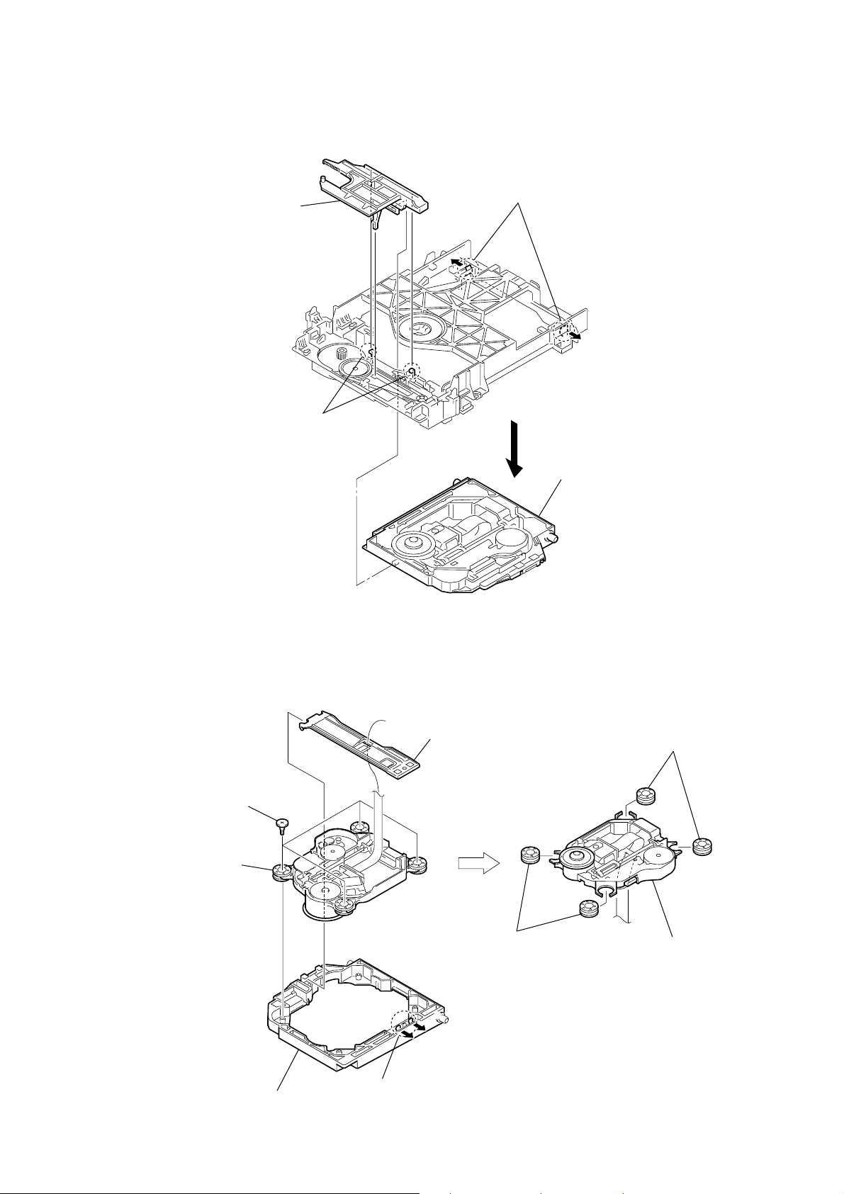
3-11. BASE UNIT
2
chuck cam
1
two claws
3
two claws
HCD-WZ88D
3-12 OPTICAL PICK-UP (KHM-310CAA/C2NP)
3
four insulator screws
4
CDM85-DVBU102
2
loading base
4
base unit (DVBU102)
5
two insulators
bu holder
1
two claws
6
two insulators
7
optical pick-up
(KHM-310CAA/C2NP)
15
Page 16
HCD-WZ88D
SECTION 4
TEST MODE
Note 1:Regarding the notification symbol “R”
Because the number of the operating buttons of this product are
limited, some operations require use of the operatingbuttons
of the remote commander, When a specific operation requires
use of the operating buttons of the remote commander, “R” is
added to the specific operating procedure in this manual.
Example MENU/NO “R” The MENU/NO button of remote
commander.
Note 2:Incorrect operations may be performed if the test mode is not
entered properly.
In this case, press the ?/1 button to turn the power off, and
retry to enter the test mode.
[P ANEL TEST MODE]
• This mode is used to check the fluorescent indicator tube,
LEDs, keys, VOLUME jog, model, destination, software
version and VACS level.
Procedure:
1. Press x button, [REC PAUSE/START] button and [DSGX]
button simultaneously.
2. All LEDs and segments in fluorescent indicator tube are lighted
up.
3. When you want to enter to the software version display mode,
press .m button. Each time .m button is pressed,
the display changes from tentative model name, software
destination, MC version, SYS version, UI version, DVD
version, ST version, TA version, TM version, TC version in
this order, and returns to the model name display. The model
name for this system is “WDZ5D”.
4. When M> button is pressed while the version numbers
are being displayed except model and destination, the date of
the software creation appears on the fluorescent indicator tube.
When M> button is pressed again, the display returns
to the software version display. When .m button is
pressed while the date of the software creation is being
displayed, the date of the software creation is displayed in the
same order of software version display.
5. Press H button, the key check mode is activated.
6. In the key check mode, the fluorescent indicator tube displays
“K 0 V0”.
Each time a button is pressed, “K” value increases. However,
once a button has been pressed, it is no longer taken into
account.
“V” value increases in the manner of 0,1, 2, 3 ... if [VOLUME+]
knob is turned clockwise, or it decreases in the manner of 0,
9, 8,7 ... if [VOLUME--] knob is turned counterclockwise.
7. When X button is pressed after all LEDs and segments in
fluorescent indicator tube light up, the fluorescent indicator
tube displays “VACS A”. A is VACS level which is triggered
by signal level.
8. When x button is pressed after all LEDs and segments in
fluorescent indicator tube light up, alternate segments in
fluorescent indicator tube would light up. If you press x
button again, another half of alternate segments in fluorescent
indicator tube would light up. Pressing x button again would
cause all segments lights off. Pressing x button again would
cause all segments lights up.
9. To release from this mode, press three buttons in the same
manner as step 1, or disconnect the power cord.
[COMMON TEST MODE]
• This mode is used to check operations of the respective sections
of Amplifier, T uner, and Tape.
Procedure:
• To enter Common Test Mode
1. Press ?/1 button to turn on the system.
2. Press x button, [REC PAUSE/START] button and
[EQ SELECT] button simultaneously.
3. The T APE A and B indicators flash on the fluorescent indicator
tube. The function is changed to VIDEO.
• Check of Amplifier
1. Press [EQ SELECT] button repeatedly until the message “GEQ
MAX” appears on the fluorescent indicator tube. GEQ
increases to its maximum.
2. Press [EQ SELECT] button repeatedly until the message “GEQ
MIN” appears on the fluorescent indicator tube. GEQ
decreases to its minimum.
3. Press [EQ SELECT] button repeatedly until the message “GEQ
FLAT” appears on the fluorescent indicator tube. GEQ set to
flat.
4. When the [VOLUME+] knob is turned clockwise even slightly,
the sound volume increases to its maximum and the message
“VOLUME MAX” appears on the fluorescent indicator tube.
5. When the [VOLUME--] knob is turned counterclockwise even
slightly, the sound volume decreases to its minimum and the
message “VOLUME MIN” appears on the fluorescent
indicator tube.
• Tape function
1. When a tape is inserted in Deck B and recording is started, the
function is changed to VIDEO automatically. When [DSGX]
button is pressed during recording in function, ALC (Automatic
Logic Control) is turned on.
2. During recording, press .m will stop the recording
and the function is changed to T APE B and re wind the tape in
Deck B until the recording start position and playback of the
tape in Deck B is started. If the [REC PAUSE/ START] button
is pressed for a pause and pressed again to resume recording
during recording time, when the tape is rewind, the tape will
be rewind until the position where the pause is applied.
• AMS T est Mode
1. Select the function “TAPE A” or “TAPE B”.
2. Select Loop or Relay direction mode by pressing the
[PROGRESSIVE/DIRECTION] button. Insert a test tape AMS110A or AMS-120 to selected tape deck.
3. Press the [CD SYNC] button to enter the AMS test mode.
4. After the test tape is rewind to the beginning of the tape, the
AMS+ is checked, and the mechanism is shut off after detecting
the AMS signal twice.
5. Then the AMS- is checked and the mechanism is shut off after
detecting the AMS signal twice.
6. When the check is complete, a message of either OK or NG
appears on the fluorescent indicator tube.
• To release from Common Test mode
1. To release from this mode, press ?/1 button.
2. The cold reset is enforced at the same time.
16
Page 17

HCD-WZ88D
[COLD RESET]
• The cold reset reset all data including preset data stored in the
RAM to initial conditions. Execute this mode when returning
the set to the customer.
Procedure:
1. Press ?/1 button to turn on the system.
2. Press x button, [CD SYNC] button, and ?/1 button
simultaneously.
3. The message “COLD RESET” appears on the fluorescent
indicator tube. Then, the fluorescent indicator tube becomes
blank for a while, and the set is reset.
[VACS ON/OFF]
• This mode is used to switch on and off the VACS (Variable
Attenuation Control System).
Procedure:
1. Press ?/1 button to turn on the system.
2. Press x button, [REC PAUSE/START] button and
[SOUND FIELD] button simultaneously. The message “VACS
OFF” or “VACS ON” appears on the fluorescent indicator
tube.
[TUNER STEP CHANGE]
• The step interval of AM channels can be toggled between 9
kHz and 10 kHz. This mode is not available for Saudi Arabian
and Russian models.
Procedure:
1. Press ?/1 button to turn on the system.
2. Press [TUNER/BAND] button repeatedly to select the “AM”.
3. Press ?/1 button to turn off the system .
4. Press x button and ?/1 button simultaneously. The system
will turn on automatically. The message “AM 9k Step” or
“AM 10k Step” appears on the fluorescent indicator tube and
thus the channel step is changed.
[DVD SHIP MODE (WITH MEMORY CLEAR)]
• This mode moves the optical pick-up to the position durable
to vibration and reset all data including preset data stored in
the RAM to initial conditions during next time you plug in
power supply. Use this mode when returning the set to the
customer after repair.
Procedure:
1. Press ?/1 button to turn on the system.
2. Select DVD function.
3. Press x button, [DVD] button and ?/1 button simultaneously.
The system will power off automatically.
4. After the “STANDBY” blinking display f inishes, the message
“MECHA LOCK” appears on the fluorescent indicator tube
and the DVD ship mode is set.
[DVD TRAY LOCK MODE]
• This mode let you lock the disc tray. When this mode is
activated, the disc tray will not open when A button is pressed.
The message “LOCKED” appears on the fluorescent indicator
tube.
[DVD COLOR SYSTEM SWITCHING]
• This mode let you change the color system of the video output
from PAL to NTSC or vice-versa. This mode is not available
for Latin American and Russian models.
Procedure:
1. Press ?/1 button to turn on the system.
2. Select DVD function.
3. Press ?/1 button to turn off the system.
4. Press X button and ?/1 button simultaneously. The system
will power on automatically.
The message “COLOR P AL” or “COLOR NTSC” appears on
the fluorescent indicator tube.
[VIDEO/SAT SWITCHING]
• This mode let you switch from VIDEO to SA T and vice-versa.
Procedure:
1. Press ?/1 button to turn on the system.
2. Select VIDEO function.
3. Press [VIDEO/SAT] button and ?/1 button simultaneously.
The function will change to SA T . Press the same b uttons again
to change from SAT to VIDEO.
[REMOTE COMMANDER DISABLE MODE]
• This mode let you disable the remote commander reception.
When this mode is activated, the system will not response if
the button on the remote commander is pressed. The message
“RM Disable” appears on the fluorescent indicator tube. Use
this mode during aging to avoid disturbance. This mode is
cancelled automatically when the system is turned off.
Procedure:
1. Press ?/1 button to turn on the system.
2. Press x button, [REC PAUSE/START] button and
[PROGRESSIVE/DIRECTION] button simultaneously. The
message “SIRCS OFF” appears on the fluorescent indicator
tube.
• To release from this mode
Press the same buttons again. The message “SIRCS ON” appears
on the fluorescent indicator tube.
[AUT O TUNING MODE]
• This mode let you tuned in any radio station automatically
without using the remote commander.
Procedure:
1. Press ?/1 button to turn on the system.
2. Press [TUNER/BAND] button repeatedly to select the “FM” or
“AM”.
3. Press x button and [TUNER/BAND] button simultaneously
and hold down until the “AUTO” lights up in the fluorescent
indicator tube and the frequency indication starts to change.
(around 3 seconds). Scanning stops automatically when a
station is tuned in.
Procedure:
1. Press ?/1 button to turn on the system.
2. Select DVD function.
3. Press x button and A button simultaneously and hold down
until the message “LOCKED” or “UNLOCKED” appears on
the fluorescent indicator tube (around 5 seconds).
17
Page 18
HCD-WZ88D
[SELECTOR MUTE RELEASE MODE]
• This mode let you output the audio signal during function other
than DVD function when the DVD decoder has been
disconnected. This system cannot output the audio signal in
the normal condition if the DVD decoder is disconnected.
Procedure:
1. Press ?/1 button to turn on the system.
2. Press x button, [REC PAUSE/START] button and
[VIDEO/SAT] button simultaneously. The message “SEL
MUTE OFF” appears on the fluorescent indicator tube.
3. Insert a microphone into the microphone jack. The audio signal
is outputted.
• To release from this mode
Press ?/1 button to turn off the system.
[DVD SERVICE MODE]
• This mode let you make diagnosis and adjustment easily by
using the remote commander and the TV. The instructions,
diagnostic results, etc. are given on the on-screen display.
Procedure to enter to DVD Service Mode:
1. Press ?/1 button to turn on the system.
2. Select DVD function.
3. Press x button and A button simultaneously and then turn
the [VOLUME+] knob clockwise.
4. The message “SERVICE IN” appears on the fluorescent
indicator tube and the T op Menu of Remocon Diagnosis Menu
appears on the on-screen display on the TV. The model name
and revision number is displayed at the bottom of the on-screen
display.
Remocon Diagnosis Menu
0. External Chip Check
1. Servo Parameter Check
2. Drive Manual Operation
3. Emergency History
4. Version information
5. Video Level Adjustment
Model Name : WDZ5D-GA
IF-con : Ver. 01.00 (0000)
Syscon : Ver. 1.311
5. To execute each function, press its number by using numeric
button on the remote commander.
6. To release from this mode, press ?/1 button to turn off the
system.
2. Select “3. Manual Adjustment” by pressing the 3 “R” button
on the remote commander. The following screen appears on
the on-screen display.
Manual Adjust
1. Track Balance Adjust:
2. Track Gain Adjust:
3. Focus Balance Adjust:
4. Focus Gain Adjust:
5. Eg boost Adjust:
6. Iop:
7. TRV. Level:
8. S curve(FE) Level:
9. RFL(PI) Level:
0. MIRR Time:
X x Change Value
RETURN
Return to previous menu
3. Select “6. Iop:” by pressing 6 “R” button on the remote
commander.
4. Wait until a hexadecimal number appear in the on-screen
display as below:
Manual Adjust
1. Track Balance Adjust:
2. Track Gain Adjust:
3. Focus Balance Adjust:
4. Focus Gain Adjust:
5. Eg Boost Adjust:
6. Iop: ED:
7. TRV. Level:
8. S curve(FE) Level:
9. RFL(PI) Level:
0. MIRR Time:
X x Change Value
RETURN
Return to previous menu
5. Convert data from hexadecimal to decimal by using con version
table.
6. Press RETURN “R” button on the remote commander to
return to previous menu.
7. Press 0 “R” button on the remote commander to return to the
Top Menu of Remocon Diagnosis Menu.
8. Press ?/1 button to turn off the system.
• Check Emergency History
To check the emergency history, please follow the following
procedure.
• Execute IOP Measurement
In order to execute mirror time adjustment, the following standard
procedures must be followed.
1. From the Top Menu of Remocon Diagnosis Menu, select “2.
Drive Manual Operation” by pressing the 2 “R” button on
the remote commander. The following screen appears on the
on-screen display.
Drive Manual Operation
1. Servo Control
2. Track/Layer Jump
3. Manual Adjustment
4. Tray Aging Mode
5. MIRR time adjust
0. Return to top Menu
18
1. From the T op Menu of Remocon Diagnosis Menu, select “3.
Emergency History” by pressing the 3 “R” button on the
remote commander. The following screen appears on the onscreen display.
Emg. History Check
Laser Hours CD 999h 59min
1. 01 05 04 04 00 92 46 00
00 00 00 00 00 00 23 45
2. 02 02 01 01 00 A9 4B 00
00 00 00 00 00 00 23 45
Next
Next Page
0
Return to Top Menu
DVD 999h 59min
Prev
Prev Page
Page 19

HCD-WZ88D
2. Y ou can check the total time when the laser is turned on during
playback of DVD and CD from the abov e menu. The maximum
time, which can be displayed are 999h 59min.
3. You can check the error code of latest 10 emergency history
from the above menu. To view the previous or next page of
emergency history, press . “R” or . “R” on the
remote commander. The error code consists of
(a) Error Code
Example of Error code
1. 01 05 04 04 00 92 46 00
00 00 00 00 00 00 23 45
The meaning of error code is as below:
01: Communication error (No reply from syscon)
02: Syscon hung up
03: Power OFF request when syscon hung up
19: Thermal shutdown
24: MoveSledHome error
25: Mechanical move error (5 Changer)
26: Mechanical move stack error
30: DC motor adjustment error
31: DPD offset adjustment error
32: TE balance adjustment error
33. TE sensor adjustment error
34. TE loop gain adjustment error
35. FE loop gain adjustment error
36. Bad jitter after adjustment
40. Focus NG
42. Focus layer jump NG
52. Open kick spindle error
51: Spindle stop error
60: Focus on error
61: Seek fail error
62: Read Q data/ID error
70: Lead in data read fail
71: TOC read time out (CD)
80: Can’t buffering
81: Unknown media type
(b) Parameter of error code
This is the detail of error code.
Example of Error code
1. 01 05 04 04 00 92 46 00
00 00 00 00 00 00 23 45
(c) Time of error code
This is the laser time when an error occurred.
Example of Error code
1. 01 05 04 04 00 92 46 00
00 00 00 00 00 00 23 45
To clear the Laser Hour
Press
DISPLAY “R” button and then press CLEAR “R” button.
The data for both CD and DVD data are reset.
Emg. History Check
Laser Hours CD 0h 0min
1. 01 05 04 04 00 92 46 00
00 00 00 00 00 00 23 45
2. 02 02 01 01 00 A9 4B 00
00 00 00 00 00 00 23 45
Next
Next Page
0
Return to Top Menu
DVD 0h 0min
Prev
Prev Page
To clear the Emergency History
Press MENU “R” button and then press CLEAR “R” button. The
error code for all emergency history would be reset.
Emg. History Check
Laser Hours CD 999h 59min
1. 00 00 00 00 00 00 00 00
00 00 00 00 00 00 00 00
2. 00 00 00 00 00 00 00 00
00 00 00 00 00 00 00 00
Next
Next Page
0
Return to Top Menu
DVD 999h 59min
Prev
Prev Page
To return to the Top Menu of Remocon Diagnosis Menu
Press 0 “R” button on the remote commander.
• Check Version Information
To check the version information, please follow the following
procedure.
1. From the Top Menu of Remocon Diagnosis Menu, select “4.
Version Information” by pressing the 4 “R” button on the
remote commander. The following screen appears on the onscreen display.
Version information
Firm (Main) : Ver. xxxxx
Firm (Sub) : xxxxx
RISC : xxxxx
8032 : xxxxx
Audio DSP : xxxxx
Servo DSP : xxxxx
0
Return to Top Menu
To return to the Top Menu of Remocon Dia gnosis Menu, press
0 “R” on the remote commander.
19
Page 20
HCD-WZ88D
B
These are omitted.
CQE
B
These are omitted.
CE
Q
SECTION 5
DIAGRAMS
THIS NOTE IS COMMON FOR PRINTED WIRING BOARDS AND SCHEMATIC DIAGRAMS.
(In addition to this, the necessary note is printed in each block.)
For Schematic Diagrams.
Note:
• All capacitors are in µF unless otherwise noted. (p: pF)
50 WV or less are not indicated except f or electrolytics and
tantalums.
• All resistors are in Ω and 1/
specified.
• f : internal component.
• 2 : nonflammable resistor.
• 5 : fusible resistor.
• C : panel designation.
Note: The components identified by mark 0 or dotted
line with mark 0 are critical for safety.
Replace only with part number specified.
✩ IC103 (EEP ROM) can not be replaced individually.
Replace it with DMB10 board assembly for service
• A : B+ Line.
• B : B– Line.
• H : adjusment for repair.
•Power voltage is fed with DXA-WZ88D from external connector (SYSTEM CONTROL 1, 2).
•Voltages and waveforms are dc with respect to ground under no-signal (detuned) conditions.
•Voltages are taken with VOM (Input impedance 10 MΩ).
Voltage v ariations ma y be noted due to normal production
tolerances.
•Waveforms are taken with a oscilloscope.
Voltage v ariations ma y be noted due to normal production
tolerances.
no mark : DVD STOP
• Circled numbers refer to waveforms.
• Signal path.
F : AUDIO
f : AUDIO IN
L : VIDEO
j : PB (TAPE)
k : REC (TAPE)
J : CD PLAY
c : DVD PLAY
I : SACD PLAY
d : TUNER
E : Y
a : CHROMA
r : COMPONENT VIDEO
N : MIC
•Abbreviation
AR : Argentine model.
AUS: Australian model.
E3 : 240 V AC area in E model.
E12 : 220-240 V AC area in E model.
E13 : 220-230 V AC area in E model.
E15 : 220-240 V AC area in E model.
E51 : Chilean and peruvian models.
EA : Saudi Arabia model.
PL : Phillippines model.
SP : Singapore and Malaysia models.
TH : Thai model.
4
W or less unless otherwise
For Printed Wiring Boards.
Note:
• X : parts extracted from the component side.
• Y : parts extracted from the conductor side.
•
• Indication of transistor.
: Pattern from the side which enables seeing.
Caution:
Pattern face side: Parts on the pattern face side seen from
(SIDE B) the pattern face are indicated.
Parts face side: Parts on the parts face side seen from
(SIDE A) the parts face are indicated.
C
Q
B
E
These are omitted.
20
Page 21
HCD-WZ88D
• Circuit Boards Location
DMB10 board
FUNCTION SW
board
MEMO
4CH-VOL board
VIDEO board
FL board
MAIN board
VR board
MIC board
MS-203 board
REGULATOR board
HCD-WZ88D
2121
Page 22
HCD-WZ88D
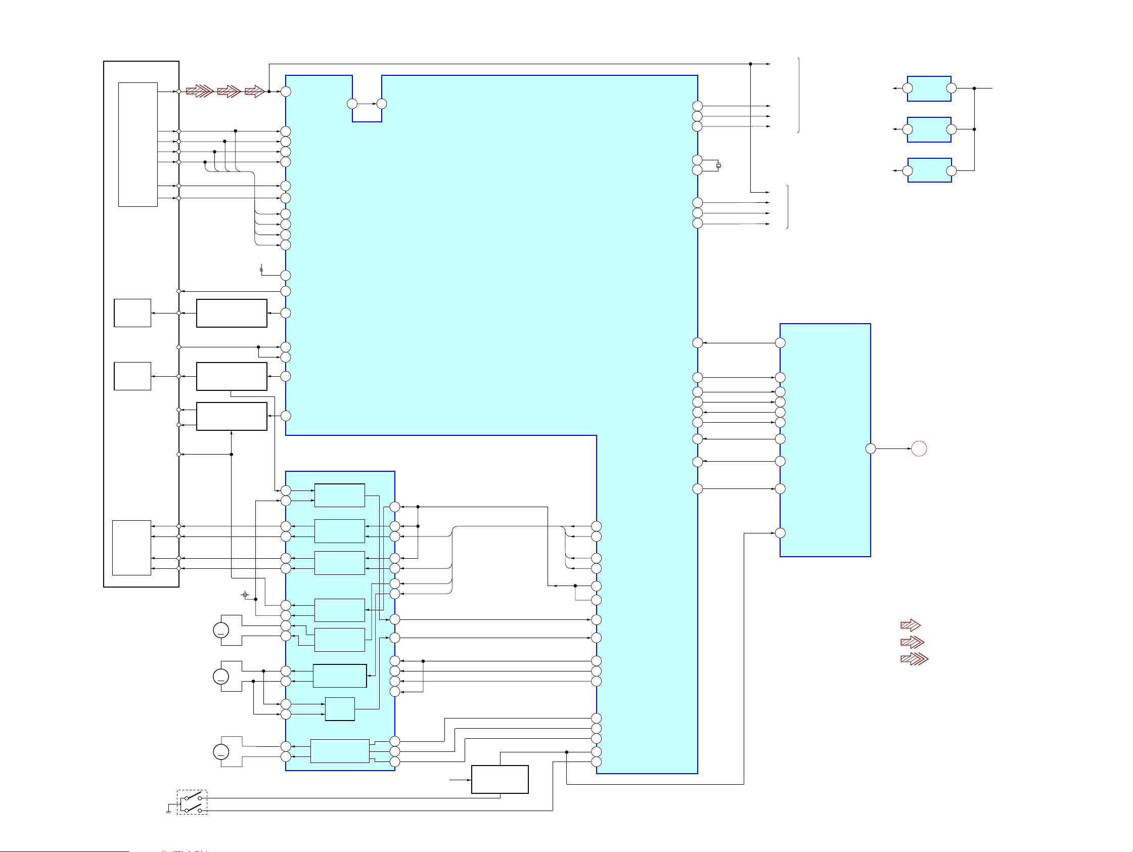
5-1. BLOCK DIAGRAM – RF/SERVO SECTION –
RFMON
RF
DETECTOR
OPTICAL PICK-UP
BLOCK
(KHM 310 CAA/C2NP)
VC
LASER
DIODE
(FOR CD)
LASER
DIODE
(FOR DVD)
2AXIS
DEVICE
FOCUS/
TRACKING
COIL
CD LD
PD
DVD LD
VR650
VR780
VCC
FCS+
FCS–
TRK+
TRK–
COADING MOTOR
A
B
C
D
F
E
(SPINDLE)
M203
C
D
Q102 (1/2)
AUTOMATIC POWER
CONTROL (FOR CD)
Q102 (2/2)
AUTOMATIC POWER
CONTROL (FOR DVD)
Q101, Q103
VOLUME CONTROL
M2
MM
(SLED)
M1
MM
MM
S001
IC107
DVDRFIP
6
OSP
252 253
DVDA
2
DVDB
3
DVDC
4
DVDD
B
A
SW+3.3V
+3.3V
SP+
SP–
5
19
TPI
18
A
B
D
C
SL–
SL+
TNI
8
NA
9
NB
10
MD
11
MC
176
LI M SW
V20
29
23
LD01
20
MD12
MD11
21
LD02
22
MSW
187
FOCUS/TRACKING COIL DRIVER,
SPINDLE, SLED MOTOR DRIVER
42
41
36 48
37 1
35 3
34 4
32
31
30
29
27
28
47
46
24
25
IC201
BUFFER
FOCUS COIL
DRIVE
TRACKING COIL
DRIVE
SLED MOTOR
DRIVE
SPINDLE MOTOR
DRIVE
BUFFER
LOADING MOTOR
DRIVER
TSD
OSN
43
10
13
40
45
19
20
22
21
TROPENPWM
15
FWD
16
REV
17
IC102 (1/3)
CD/DVD RF AMP,
FOCUS/TRACKING ERROR AMP
DVD SYSTEM PROCESSOR
DIGITAL SERVO PROCESSOR
VREF0
FOO
TRO
FMO
DMO
SW+3.3V
Q2001
VOLTAGE DETECT
OCSW
CKSW
VREF0
FMO
FOO
DMO
TRO
38
FMO
42
FOO
37
DND
41
TRO
V REFO
30
246
V REFO
40
IOPMON
47
SPFG
184
MUTE123
183
MUTE
181
TSDM
TROPENPWM
39
FWD
186
REV
185
OCSW
177
CKSW
179
V2REF0
RXD
TXD
XTALO
XTALI
FED
TEO
RFLVL
PRST
IFCK
MREQ
IFSDO
IFSDI
XIFCS
MIC/VSYNC
IFBSY
KRMOD/HSYNC
28
106
107
228
229
31
32
26
110
99
114
98
101
100
205
105
207
X101
27MH
Z
RF
FE
TE
PI
V2REF0
RXD
TXD
38
MTK_RESET
MTK_CLK
33
35
REQ
32
MTK_SOD
31
SID
27
XIFCK
26
MIC_STATUS
28
IFBUSY
24
KRMOB
87
OPEN_SW
for TEST
for TEST
VIDEO_MUTE
IC401 (1/3)
SYSTEM
CONTROLLER
RF +3.3V
+3.3V
+1.8V
37
4 1
4 5
3 1
VMUTE
SECTION
(Page 23)
• Signal Path
+3.3V REG
IC105
+3.3V REG
IC106
+1.8V REG
A
VIDEO
SW +5.5V
: CD PLAY
: DVD PLAY
:SACD PLAY
HCD-WZ88D
2222
Page 23
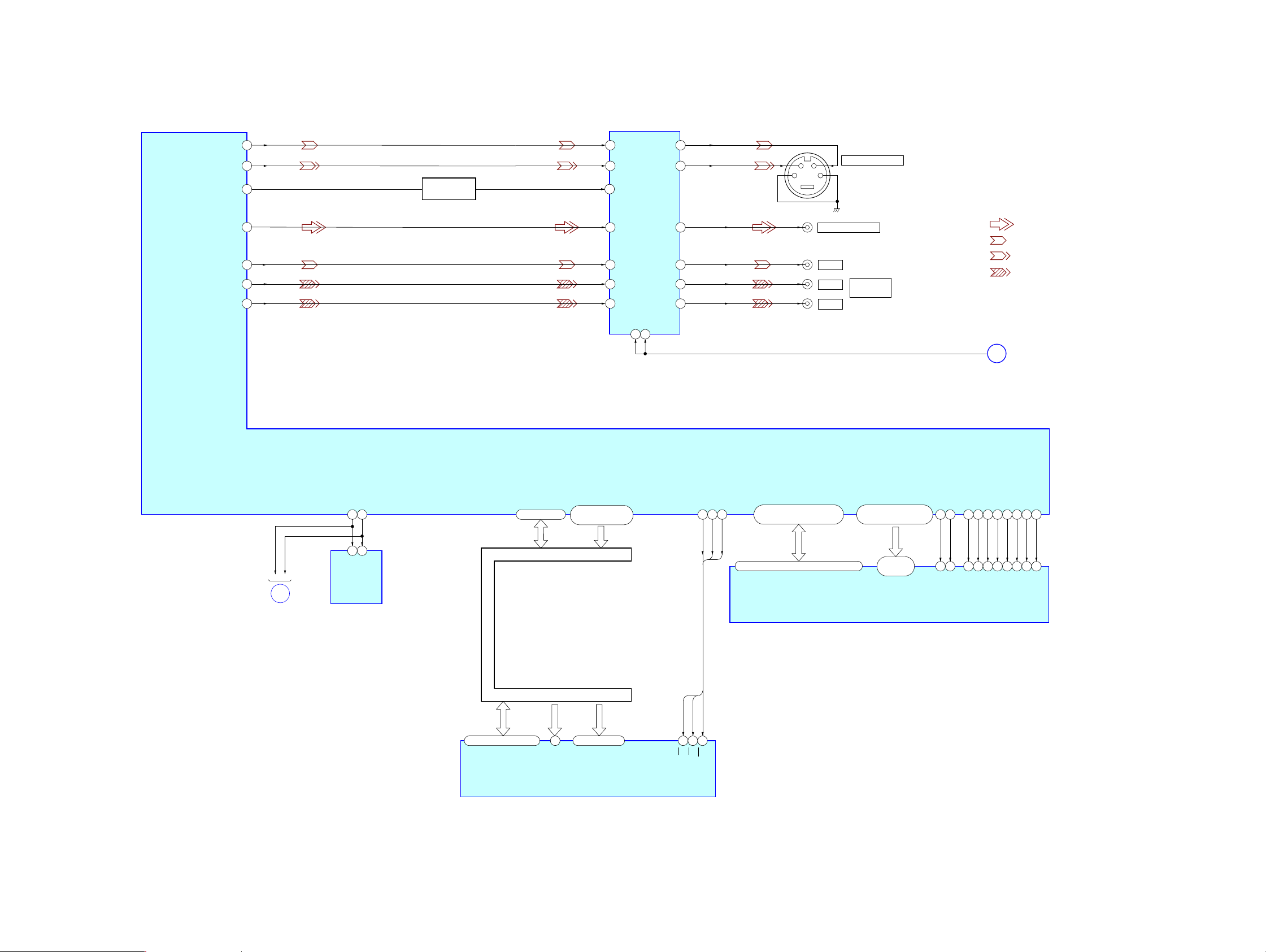
– VIDEO SECTION –
YUV1
YUV2
WODE
YUV3
YUV4
YUV5
YUV6
HCD-WZ88D
IC801
VIDEO AMP, 75Ω DRIVER
Y
194
C
196
171
V
198
200
202
203
Y/G
Cb
Cr
Q800
WIDE SWITCH
10
12
14
6
2
9
4
YIN
CIN
I/P
CVBSIN
CYIN
CBIN
CRIN
MUTE1
3
CVBSOUT
CYOUT
CBOUT
CROUT
MUTE2
13
YOUT
COUT
21
26
21
43
J801
S VIDEO OUT
• Signal Path
VOUT
23
J802
VIDEO OUT
: VIDEO
: Y
CYOUT
20
CBOUT
18
CROUT
16
P
P
Y
B / CB
R / CR
J803
COMPONENT
VIDEO OUT
VMUTE
: CHROMA
: COMPONENT VIDEO
RF/SERVO
A
SECTION
(Page 22)
SCL
SDA
B
AUDIO
SECTION
(Page 24)
SCL
102
103
6 5
SCL
IC103
EEPROM
SDA
SDA
IC102(2/3)
DVD SYSTEM PROCESSOR
AD0 – AD7
81-84,86-88,91
HD0 – HD7 A0 – A21
DATA & ADDRESS BUS
DATA & ADDRESS BUS
HD0 – HD7
29,31,33,35,38,40,42,44 25-16,10-1, 48
DQ0 – DQ7
HIGHA0-7
IOA0-7, IOA18-IOA20
A16, A17
53-61, 67-72, 74-76,
78, 89, 92, 93
A0
A0 – A19DQ15/A-1
IC101
FLASH ROM
A1-A21
XRD
XROMCS
2645
28OE11
CE
IOCS
77
79
XRD
XROMCS
XWR
WE
IOWR
IOUE
66
XWR
2,4,5,7,8,10,11,13,42,44,45,47,48,50,51,53
RD0 – RD15
125-123, 121, 120, 118,
117, 115, 135, 133-128, 126
RD0 – RD15
RA0 – RA11
146, 147, 149-151,
158-160, 162, 164-166
22-26,
29-35
RA0 – RA11
IC104
SDRAM
RCLK
RCS
RWE
MRAS
BA0
BA1
143
20
142
145 156 113 137 157
38
19
21
BS0
BS1
DRCLK
138
RCS
CAS
140
139
16
18
17
CAS
RAS
RWE
MDQM0
15
DQM0
MDQM1
39
DQM1
CKE
37
DRCKE
HCD-WZ88D
2323
Page 24

HCD-WZ88D
– AUDIO SECTION –
IC102(3/3)
DSP
ASDATA0
ASDAT1
ASDATA2
ALRCK
ABCK
ALCK
XRST
SPDATA/SMSDI
IC301
D/A CONVERTER
IC3711(1/2)
FL
2
LOUT1+
1
DATA0
DATA1
BCK
LRCK
XCK
DATA2
LRCK
BCK
XCK
XRST
B
IC3601
A/D CONVERTER
12
DOUT
11
BCK
10
LRCK
15
SCKI
SCL
SDA
LIN
RIN
217
218
219
213
214
215
220
209
DATA0
DATA1
DATA2
XRST
LRCK
BCK
XCK
ADC_DATA
VIDEO
SECTION
(Page 23)
ADC_DATA
ANALOG-IN-L
1
2
14
SDTI1
15
SDTI2
16
SDTI3
17
LRCK
9
BICK
10
MCLK
8
PDN
34
MDI
35
MC
R-CH
LOUT1-
ROUT1+
ROUT1-
LOUT2+
LOUT2-
ROUT2+
ROUT2-
LOUT3+
LOUT3-
ROUT3+
ROUT3-
LOUT4+
LOUT4-
ROUT4+
ROUT4-
L
FR
48
47
SL
46
45
SR
44
43
C
42
41
SW
40
39
DM_L
38
37
DM_R
33
32
MAIN
SECTION
(Page 25)
IC3711(2/2)
IC3731(1/2)
IC3731(2/2)
IC3751(1/2)
IC3751(2/2)
IC3771(1/2)
IC3771(2/2)
DVD MUTE
Q276,277
MUTE
CONTROL
Q304
MUTE
Q305
MUTE
Q307
MUTE
Q308
MUTE
Q306
MUTE
Q309
MUTE
Q302
MUTE
Q303
MUTE
41
FL-IN
2
FR-IN
6
SL-IN
10
SR-IN
13
C-IN
14
LFE-IN
37
DM-L
40
DM-R
IC301
SOUND PROCESSOR
SURROUND-IN-L
SURROUND-IN-R
DATA
CLK
17 18
FL-OUT
FR-OUT
SL-OUT
SR-OUT
C-OUT
L-OUT
R-OUT
SW-IN
SW-OUT
34
32
29
26
25
38
39
3
7
15
22
SURROUND-IN-L
SURROUND-IN-R
Q274,275
MUTE
CONTROL
Q301
MUTE
FL
FR
SL
SR
C
DOWNMIX-L
DOWNMIX-R
VRSWIN
SW
SECTION
M
(Page 25)
DXA-WZ88D (1/3)
REAR-L
REAR-R
DVD MUTE
CENTER
SECTION
N
(Page 25)
MAIN
SECTION
O
(Page 25)
MAIN
SECTION
P
(Page 25)
SUB WOOFER OUT
MAIN
DVD MUTE
MAIN
J302
21
DVD-A-MUTE
IC401 (2/3)
SYSTEM CONTROL
50 49
VOL-IC-CLK
VOL-IC-DATA
48
SW MUTE
DVD MUTE
• R-ch is omitted due
to same as L-ch.
• Signal Path
: AUDIO
HCD-WZ88D
2424
Page 25

– MAIN SECTION –
J101(1/2)
L
VIDEO SAT
J701
IN
MIC1
R
R-CH
m
J702
MIC2
m
TUNER UNIT
+9V
L OUT
R OUT
ST D OUT
ST DIN
ST CLK
ST CE
TUNED
DXA-WZ88D(2/3)
PB-L
PB-R
REC-L
REC-R
TA MUTE
• R-CH is omitted due to same as L-CH.
• Signal Path
: AUDIO
: TUNER
: AUDIO IN
: MD
: PB (TAPE)
: REC (TAPE)
: MIC
ST A+9V
R-CH
R-CH
R-CH
MUTE
Q501
MUTE
Q502
PB SW
Q581,582
IC702(1/2)
MIC AMP
31
Q521,523
Q522,524
IC581
MUTE
CONT
MUTE
CONT
Q583-585
AMS
RV702
MIC LEVEL
3
Q520
IC501
REC
AMP
HCD-WZ88D
IC101
SOUND PROCESSOR
37
R-CH
RECT
Q272,273
MUTE
CONT
D+3.3V
D294
D295
39
38
40
35
41
19
21
22
D+4V
µCOM
µCOM
+VCC
N
L
9
DOWNMIX-L
ANALOG-IN-L
RV701
ECHO LEVEL
R-CH
R-CH
+
CN401
JIG
IC702(2/2)
MIC AMP
67
MUTE
D+3.3V
IC640
REMOTE
CONTROL
RECEIVER
I2CDATA
I2CCLK
X401
32.768kHz
X402
5MHz
1
MIC-DETECT
45
ST-DOUT
46
ST-DIN
47
ST-CLK
44
ST-CE
43
TUNED
TC-MUTE
55
ALC
56
57
REC-MUTE
AMS-IN
54
66
LINE-MUTE
(TA MUTE)
4SIRCS
IIC DATA
30
30
IIC CLK
29
XC-IN
10
XC-OUT
11
X-IN
15
X-OUT
13
IC401(3/3)
SYSTEM CONTROL
AUDIO-IC-DATA
AUDIO-IC-CLK
HP/REC OUT MUTE
HEADPHONE IN
ANALOG IN MUTE
IO-EXP DATA IN
IO-EXP DATA OUT
FL-DRIVER-DATA
FL-DRIVER-CLK
FL-DRIVER-CS
FL-DRIVER-RESET
DISPLAY KEY
LED-SOUND MODE
LED-VIDEO/SAT
LED-TAPE A/B
LED TUNER/BAND
IF-DVD-POWER
VACS IN
IO EXP CLK
IO EXP LAT
STK POWER
A SHUT
B SHUT
A TRG
B TRG
CN CHECK
AD KEY2
VOL A
VOL B
POWER KEY
LED-DVD
AC-CUT
AUDIO
SECTION
(Page 24)
97
52
51
77
63
22
59
58
61
60
65
89
90
91
88
53
81
82
83
100
95AD KEY1
94
67
68
74
73
75
69
71
70
72
76STBY-LED
20
12RESET
3039
Q105
MUTE
MUTE
CONT
Q293
RESET
SWITCH
Q278,279
63
IC610
62
FL DRIVER
61
60
Q664-668
LED
DRIVE
Q641
LED
DRIVE
3
M
FL1
FL2
VFL
S651-652
S641-644
FUNCTION
KEY
S650
4 DIRECTION
SWITCH
S653-655
FUNCTION
KEY
S656
5 DIRECTION
SWITCH
S661
VOLUME
ENCODER
S642
I/
S643
DISPLAY
D664-668
D641
IC251
RESET
Q191
VACS
F-L
Q610,611
GRID
DRIVER
VFL
VOLUME
(STANDBY)
1
D601 – 604
PUSH ENTER
PUSH ENTER
AUDIO
SECTION
(Page 24)
AUDIO
SECTION
(Page 24)
IC701
ECHO
2
AMP
2
5
IND2
INB2
INC2
2
MIC
INA2
REC B2
SUR2
SA OUT
DATA
CLOCK
DC/DC CONVERTER
T601
FL601
FLOURESCENT
INDIDATOR
TUBE
REC A2
OUT2
BB A2
BB B2
D402
D403
36
25
27
26
24SW OUT
29TOUT
OSC
Q602
+SW3.3V
(DMB10)
D/DCON+9V
+SW9V
3
IC906
+3.3V
REG
+SW5V
V +5V
Q101
DBFB
1
Q270
MUTE
IC903
+9V
2
Q903,904
DVD PWR
CONTROL
REG
HEADPHONE AMP
IC103
31
Q171
MUTE
1
5
AU+9V
ST A+9V
A+4.5V
HP AMP
D/DCON+9V
Q161
RIPPLE
FILTER
Q182
RIPPLE
FILTER
LED +9V
IC913
2
D911-D913
+5V
REG
5
R-CH
R-CH
R-CH
1
3
VRSWIN
SURROUND-IN-L
R CH
D901
IC901
+9V
1
REG
J101(2/2)
L
VIDEO SAT
OUT
R
J703
i
AUDIO
SECTION
P
(Page 24)
AUDIO
O
SECTION
(Page 24)
DXA-WZ88D(3/3)
HP MUTE
FRONT-L
FRONT-R
DBFB FB
IO EXP DATA OUT
IO EXP DATA IN
IO EXP CLK
IO EXP LAT
STK MUTE
A SHUT
B SHUT
A TRG
B TRG
CN CHECK
EVER +4V
M +9V
DVD AC
DVD AC
AMP +9V
UNREG
HCD-WZ88D
2525
Page 26

HCD-WZ88D
5-2. PRINTED WIRING BOARD – DMB10 SECTION (SIDE A) –
12
A
C
VIDEO
BOARD
CN801
(Page 41)
B
• See page 21 for Circuit Boards Location.
3456
:Uses unleaded solder.
EXCEPT
TH
E
✩ IC103 (EEP ROM) can not be replaced individually.
Replace it with DMB10 board assembly for service
4CH-VOL
BOARD
CN303
A
(Page 39)
2
1
CN302
18
19
• Semiconductor
Location
Ref. No.
D1001 C-5
D3501 A-4
D3502 A-4
IC101 D-3
IC102 C-3
IC103 C-4
IC104 C-4
IC106 C-5
IC201 D-5
Q103 C-2
Q3801 B-4
Location
C
D
OPTICAL
PICK-UP
BLOCK
(KHM-310CAA)
for
CHECK
MAIN
BOARD
CN101
(Page 32)
D
E
R1111
IC102
IC103
IC104
1
5
IC106
B
REGULATOR
C 228
C 223
C 227
IC201
IC101
C 226
C 226
R 243
C 225
1
5
CN 202
2
4
1 5 4 5
12
10
13
11
BOARD
CN506
(Page 37)
for
TEST
HCD-WZ88D
E
E
MS-203
BOARD
CN001
(Page 41)
2626
Page 27

HCD-WZ88D
5-3. PRINTED WIRING BOARD – DMB10 SECTION (SIDE B) –
12
A
IC3601
B
• See page 21 for Circuit Boards Location.
3456
10
1
20
11
IC3711
IC3731
IC3771
IC3751
IC301
:Uses unleaded solder.
IC107
3
4
• Semiconductor
Location
Ref. No.
D3601 B-2
D3602 B-2
IC105 D-5
IC107 B-5
R308
1
5
IC301 C-3
IC3601 B-2
IC3711 B-3
IC3731 B-3
IC3751 B-3
IC3771 B-3
Q101 C-5
Q102 C-5
Q2001 E-5
Location
C
D
R222
R1555
R236
R238
S
R239
E
IC105
3
4
5
1
R237
S
S
E
HCD-WZ88D
E
2727
Page 28

HCD-WZ88D
5-4. SCHEMATIC DIAGRAM – DMB10 SECTION (1/4) –
CN401
5P
IC3601
PCM1803DBR
C3607
0.1
R3602
100
D3601
1SS355TE-17
D3602
1SS355TE-17
R314
100
C301
0.01
JL3653
IC301
AK4358VQ-L
JL3652
JL344
JL343
R3605
L3601
C3602
JL345
C3601
JL346
JL347
JL348
JL349
10
R3651
0.1
0
R3653
R3652
ICT301
0
0
R3609
0
R3601
100
R3606
0
0
• See page 45 for IC Block Diagram.
JL4601
JL4602
JL4603 JL4604
JL4605 JL4606
JL4607 JL4608
JL4609 JL4610
R3611
100
R3621
C3621
0.01
C3611
L3602
C3605
47
6.3V
2SC2712-YG-TE85L
R3803
10k
0
R3804
18k
R3802
0
C3801
R3801
0
JL3651
C3610
C3609
10
0.1 0.01
R3607
0
0.1
10 16V
C3603
R3603
16V
0.1
10k
C306
C305
100
0.47
6.3V
R319
C307
100
6.3V
C3608
C3606
C302
0.47
FL401
FB402
0UH
0UH
100
Q3801
C3805
47
4V
C3802
10
R3805
1k
C3803
*
C3804
100
6.3V
*
FB404
0UH
FL403
FB403
0UH
0UH
C402 C403
47
16V
FL402
FB401
EMI
0UH
R3743
R3741
2.2k 5.6k
C3742C3741
0.00220.0015
R3742 R3744
R3745
5.6k
2.2k
4.7k
C3743
C3704
0.1
C3703
0.1
C3733
2.2k 5.6k
2.2k
2.2k
R3712
2.2k
C3711
0.0015
R3711
2.2k
C3701
R3733
5.6k
R3723
5.6k
R3724
5.6k
0.1
R3714
5.6k
R3713
5.6k
R3735
C3732
0.0022
4.7k
R3725
4.7k
C3723
C3702
0.1
C3713
C3712
0.0022
R3732 R3734
C3731
0.0015
R3731
R3721
C3721 C3722
0.0015 0.0022
R3722
2.2k
47
6.3V
R3747 R3748
R3746
1k
470p
IC3731
NJM3414AV(TE2)
470p
R3736
R3727
R3726
1k
5.6K
470p
R3716R3715
FB406
0UH
FB405
0UH
1k 4.7k
470p
C3744
1k
R3737
1k
1k
470p
C3724
1k4.7k
R3717
1k
470
C3734
R3728
4.7k
470p
C3714
R3738
4.7k
R3719
R3718
4.7k
1k
IC3711
3414AV(TE2)
NJM
R3729
R3749
R3739
R3781 R3783
2.2k
5.6k
C3781 C3782
0.0015 0.0022
R3784
R3782
5.6k
2.2k
1k
C3707
1k
1k
0.1
R3772
R3771
2.2k
R3773
R3761
2.2k
R3763
R3762 R3764
2.2k
C3705
0.1
R3752
2.2k
R3751
2.2k
R3774
0.0015
0.0015
5.6k2.2k
C3771
C3761
C3751
R3753
5.6k
R3754
5.6k
5.6k
R3787 R3788
1k 4.7k
470p
R3786
1k
R3785
4.7k
C3783
C3708
0.1
C3773
R3775
4.7k
C3772
0.022
5.6k
5.6k
C3762
0.0022
R3765
4.7k
C3763
C3753
R3755
C3752
0.00220.0015
C3706
C3784
470p
470p
R3776
1k
R3777
1k
R3767
1k
R3766
1k
470p
0.1
470
R3756
1k4.7k
R3757
1k
470p
C3774
R3768
4.7k
C3764
470p
470
C3754
R3778
R3758
4.7k
4.7k
IC3771
3414AV(TE2)
NJM
IC3751
3414AV(TE2)
NJM
R3789
R3779
R3769
R3759
1k
1k
1k
1k
D3502
1SS355TE-17
D3501
JL3503
JL3504
JL3505
JL3506
JL3507
JL3508
JL3509
JL3510
JL3511
JL3512
JL3513
JL3514
JL3515
JL3516
JL3517
JL3518
JL3519
JL3520
JL3521
CN302
19P1SS355TE-17
HCD-WZ88D
2828
Page 29

HCD-WZ88D
5-5. SCHEMATIC DIAGRAM – DMB10 SECTION (2/4) –
28 30 31
CAA
for CHECK
31
FL101
0UH
31
CN101
24P
C101
JL139
0.01
JL140
JL141
JL142
JL143
JL144
CL112
JL145
JL146
CL113
JL147
JL148
CL114
JL149
CL115
JL150
CL116
JL151
JL152
JL153
CL117
JL154
CL118
JL155
JL156
JL157
JL158
JL159
UM6K1N-TN
31
R101
30
31
100
ICT121
ICT123
R110
47k
R107
CL106
10k
CL107
31
ICT114
ICT115
ICT117
31
72
CN103
31
5P
RF
GND
FE
TE
PI
ICT116
ICT119
ICT118
ICT112
ICT120
R126
0
ICT129
IC107
C192
TK11133CSCL-G
0.01
R116
1k
C117
10 16V
C115
0.1
Q101
ICT127
R108
R111
1M
100
R113
R112
R115
22
22
C105
47
6.3V
ICT124
R114
C106
R1129
100k
0.01
100k
R109
0
FE
TE
PI
C118
10 16V
C116
R117
0.1
47k
RT1N241C-TP-1
22
22
22
C112
ICT126
47
6.3V
120
121
R
R
R118
Q102
QST8TR
22
• See page 43 for Waveforms. • See page 46 for IC Pin Function Description.
30
z
H
6
27M
12p
05
16V
10
150
JL
JL1
C
01
52
10
X1
C1
k
1
100
0k
.00
0
75
142
R
151
141
C
R
T113
JL168
IC
C193 C195
0.22
C114
0.1
C119
10
16V
Q103
R124
47k
R123
0
C113
0.01
C120
C121
C122
C123
C124
CL1501
ICT125
p
R138
100k
22
0.110.1
0.1
0.1
39
143
140
141
C1
C
C
C132C130
0.10.1
ICT128
0.22
1
1
1
1
1
C125
0.1
PI
FE
TE
C126
0.1
C196
0.0047
R133
3.3k
R134
3.3k
R135
3.3k
C127
0.01
C128
0.0015
ICT112
CL105
C129
JL101
JL130
JL167
JL102
JL127
JL132
JL133
CL101
JL135
CL104
CL108
CL109
CL110
JL136
FL105
0UH
10
16V
5k
1
R136
C131
2.2
0.033
C133
0.1
C135
C136
0.01
C
0.1
0.001
0.1
8
37
13
C1
C
C142
C144
0.01
4
JL103
JL10
C146
C145
C149
0.1
C147
C148
0.047
0.047
28
4.7k
7
7
4
4
T133
12p
0
0
IC
6
53
154
1
1547
144
C153
R
470
0.1
8
4
C15
R116
IC102
CXD9804R
C155
9
70
0.01
JL16
JL1
151
4.7k
R
C15
0.01
R
R
R
8
154
4.7k
R
0
2
15
R
28
28
R1551
R1526 0
R1524 0
61
C1
4.7k
0
C159
0.01
R1527
10k
R1543
JL129
JL160
JL128
JL172
JL164
JL173
4
150
0
R
k
4.7
0
0
7
4
1
49
0
155
47
1530
15
16
153
R
R
R
R
R
550
1
4.7k
R
165
JL
JL166
JL171
C158
0.01
C160
100
0.01
100
R164
1557
161
100
R
R
30
0
R308
JL4701
JL4702
0
0
92
89
15
15
R1
R190
.01
0
10K
542
1
R
RB112
22
R1
C163
0.01
C164
C162
0.01
0.01
RB113
22
50
195
1102
150
1
150
R
R1120
0
R
150
R197
R1121
0
R1125
0
R1124
0
R1123
0
R1122
0
36
ICT1
R1101
2.2k
R1553
0
C170
0.01
ICT134
C171
0.01
0.01
C172
R1108
*
R1554
4.7k
C175
0.01
C176
0.01
JL163
RB108
22
RB107
22
CL120
JL161
JL162
JL113
R196
0
C177
47
6.3V
R4701
0
JL4703
JL4704
JL4705
JL4706
R4702
0
JL4707
JL4708
R4703
0
JL4709
JL4710
R4704
0
JL4711
JL4712
R4705
0
JL4713
R4706
0
CN301
13P
VIDEO
42
28 30 31
R1103
10k
10k
R1104
10k
R1105
ICT138
73
31
31
R1107
0
R1109
0
R1111
C173
0
0.01
C174
0.01
RB104
RB111
ICT109
ICT130
ICT1501
4.7k
R1555
0
RB103
0
0
R1108
*
0:TH
10K:EXCEPT
TH
74
31
31
30
FL106
0UH
HCD-WZ88D
30
2929
Page 30

HCD-WZ88D
5-6. SCHEMATIC DIAGRAM – DMB10 SECTION (3/4) –
IC101
MBM29DL32TF-70
29 29
✩ IC103 (EEP ROM) can not be replaced individually.
Replace it with DMB10 board assembly for service
C181
0.1
RB106
47
C180
0.1
C191
0.1
RB105
0
R104
R105
10k
R106
10k
0
CN106
CN105
R1545
13P
6P
JL108
JL109
JL110
JL111
JL112
JL138
JL114
JL115
JL116
JL117
JL118
JL119
JL120
JL121
JL122
JL123
JL124
JL125
71
OCSW1
31
33
KRMOD
C102
0.01
R169
10k
R1133
R1134
ICT110
ICT111
0
IC106
PQ018EZ01ZPH
0
FL104
0UH
R193
R191
1k
IC103
ICT104
ICT106
ICT102
R1546
3.3k
ICT107
ICT101
ICT103
ICT105
0.001
C108
R1110
ICT137
FB111
0UH
FB112
0.001
C109
2.7k
R1502
FB113
FB114
FB115
0UH
0UH
0UH
0
0UH
R1150
R1152
3.3k
R1151
3.3k
3.3k
BR24L64F-WE2
C167
0.01
1k
FL107
0UH
C178
47
4V
IC104
HY57V64162
0HGTP-HDR
ICT108
C184
0.01
C182 C188
0.22 0.22
IC105
TK11133CSCL-G
C189
0.33
R187
0
D1001
RB501V-40TE-17
C179
0.1
FL108C190
0UH47 6 . 3V
C187
47
4V
47
28 29 31
29
28 29 31
HCD-WZ88D
KRMOD
101
29
MIC
29
SCL
100
SDA
28
3030
Page 31

5-7. SCHEMATIC DIAGRAM – DMB10 SECTION (4/4) –
29
HCD-WZ88D
28 29 30
29
29
CL205
C211
0.033
R225
100k
R226
R232
18k
CL207
CL208
R234
R233
33k
10k
C215
0.01
C217
16V
CL209
CL210
CL211
CL212
C219
0.01
C224
0.01
C218
10
16V
C223
0.1
47
C220
16V
10
C221
0.1
C222
0.1
R246
4.7k
4.7k
R239
29
R238
4.7k
JL201
JL202
JL203
JL204
JL205
JL206
R247
1k
1k
R237
R236
S
1k
Q2001
2SK1828TE8
VOLTAGE
DETECT
100
R243
ICT203
0.001
C226
ICT204
0.001
C225
JL207
JL208
JL209
JL210
JL211
CN201
6P
CN202
5P
CKSW
OCSW
OCSW1
OCSW1
CKSW1
GND
LDMLDM+
74
29
71
28 29 30
E
MS-203
CN001
CAA
29
30
42
R231
15k
R230
82k
C212
56k
0.01
0.001
C214
C213
0.01
IC201
FAN8036L
CL206
ICT207
R223
100k
R221
56k
C209
C233
0.033
0.0047
R220
R219
27k
R224
10k
10k
C210
0.01
R212
10k
C205
220p
C208
0.01
R215
12k
R216
R214
15k
12k
CL201
CL202
CL203
CL204
R208
33k
R206
10k
R209
33k
R207 C203
2.7k 0.01
R204
1.2k
R205
10k
29
R210
R213
6.8k
47k
C206
220p
28
HCD-WZ88D
29
29
R222
T R O P E N P W M
72
29
73
F W D
R E V
R228
0
R227
0
33k
29
3131
Page 32

HCD-WZ88D
5-8. PRINTED WIRING BOARD – MAIN SECTION –
12
A
B
L
R
TH
E
TH
E
• See page 21 for Circuit Boards Location.
34567 9
TUNER
F
(Page 39)
E
E
E
:Uses unleaded solder.
4CH-VOL
BOARD
CN301
E
E
E
8
DMB10
for JIG
E
E
E
E
E
E
D
BOARD
CN106
(Page 26)
For CHECK
IC251
E
C
D
E
OUT IN
VIDEO/SAT
SYSTEM CONTROL 2
(TO DXA-WZ88D)
(CHASSIS)
IC103
REGULATOR BOARD
G
CN501
(Page 37)
IC101
E
IC401
E
K
E
E
E
REGULATOR BOARD
H
CN502
(Page 37)
J
(Page 41)
MIC
BOARD
CN701
I
MIC
BOARD
CN701
(Page 41)
(CHASSIS)
FL BOARD
CN601
(Page 35)
HCD-WZ88D
• Semiconductor Location
Ref. No.
D191 D-5
D192 D-5
D193 C-8
D201 B-7
D202 B-7
D292 C-8
D293 C-8
D294 B-8
Location
Ref. No.
D295 B-8
D402 B-6
D403 B-6
IC101 C-4
IC103 D-3
IC251 B-8
IC401 C-7
Location
Ref. No.
Q101 B-4
Q105 B-3
Q151 C-4
Q155 B-4
Q161 C-5
Q171 D-4
Q181 D-4
Q182 D-4
Location
Ref. No.
Q191 C-4
Q270 B-2
Q271 B-2
Q272 B-5
Q273 B-5
Q274 B-5
Q275 B-5
Q276 B-6
Location
Ref. No.
Q277 B-6
Q278 B-7
Q279 B-7
Q293 B-8
Location
3232
Page 33

5-9. SCHEMATIC DIAGRAM – MAIN SECTION (1/2) –
HCD-WZ88D
J101
CN101
13P
CN111
R267
47k
R268
47k
CN105
23P
NO1
2SC3661-TB-E
TP449
TP464
TP450
MT
Q274
DTA114EKA
Q155
R157
C151
10k
R161
10k
R169
C101
10
50V
R111
Q105
R108R158
2SC3661-TB-E
47k47k
R107
1k
47k
47k
R119
C105
10
50V
100
100
50V
50V
0
R170
0
R115
R114
C123
100
10V
100
10
50V
50V
10
C104
100
R122
50V
10
C152
C154C124
20
10
10
R135
R1
C103
C102
C153
10
50V
R145
100
10
50V
C106
0.022
C272
100
10V
R101
2.2k
C108
R102
0.022
10k
C107
IC101
M61529FP-D60G
0.022
0.068
0.022
C156
C159
C157
R152
10k
C158
R151
2.2k
50V
R280
100k
50V
10
R277
220
C271
R276
100
22k
10V
10
0.0033
C111
10
0.15
50V
C110
0.0033
C161
C160
10
50V
Q151
2SC2412K
0.15
C162
C112
0.27
C163
0.068
C109
10
50V
1k
C155
10
50V
0.27
C113
R269
100k
R153
10k
1k
R104
DTC114EKA
R154
1k
C269
2.2
50V
Q275
R103
R112
10k
TP452
R113
TP451
Q272
DTA114EKA
R273
220
R272
22k
C270
2.2
50V
2SC2412K
10k
10k
R168
330
Q101
C166
100
10V
Q161
2SC3661
DTC114EKA
C125
0.1
R155
100k
C129
Q273
R105
100k
R140
1M
C140
1
50V
10V
100
C126
10
50V
R193
22k
68k
R194
2SC2412K
Q191
C165
R167
4.3k
R166
3.3k
NO2
MT
1k
R197
C133
10
50V
R196
330
10
100
50V
50V
C134
47
R195
0.1
C400
TP401
NO807
4P
CN110
16P
TP439
C242
0.1
TP3
C244
0.1
TP1
TP2
CN104
9P
C119
0.1
Q270
2SC3661
Q271
2SC3661
0
R291
TP443
100
25V
R274
1k
R265
47k
R266
47k
R275
1k
TP447
TP446
TP444
TP445
0
R241
C174
C173
R174
10 50V
220p
C183
C171
220p
C181
220p
C175
0.1
D201
1SS355TE
D202
1SS355TE
C201
0.1
220p
100k
R172
100k
R182
100k
R184
C184
10 50V
C182
10
50V
100k
C172
10 50V
R270
R271
C180
1k
1k
R173
1k
R183
1k
JR1
0
R171
1k
R181
1k
16P
TP466
TP465
TP454
TP455
TP456
TP457
TP424
TP4
TP426
TP433
TP435
TP432
TP431
TP428
TP427
TP438
TP487
C227
0.01
HCD-WZ88D
C402
0.1
3333
Page 34

HCD-WZ88D
5-10. SCHEMATIC DIAGRAM – MAIN SECTION (2/2) –
NO808
4P
TP463
EP101
CN107
15P
TP492
TP490
TP491
TP489
TP461
TP460
TP459
TP458
TP453
C114
CN109
10 50V
23P
TP476
TP475
TP474
TP473
TP481
TP482
TP483
TP500
TP472
TP471
TP470
TP469
TP468
TP467
TP495
TP494
TP404
C403R106
0.10
C121
1000
10V
C120
0.1
• See page 43 for Waveforms. • See page 51 for IC Pin Function Description.
R180
10k
R190
C164
10 50V
Q171
2SC3661
R177
100k
R149
R179
22
22
C177
220
10V
R176
47k
C170
22p
R178
R175
1k
10k
C179
10
R150
50V
R156
0
47k
Q278
DTA114EKA
C194
100 10V
C193
1000
10V
NJM3414AM-TE2
R198
1k
DTC114EKA
Q276
DTA114EKA
10k
Q181
2SC3661
100
10V
R284
DTC114EKA
R159
R189
22
22
C187
220
10V
R186
47k
22p
C190
R185
R188
10k
1k
C189
R160
10
47k
50V
R481
Q182
2SD2525
R283
22k
100
10V
100k
Q277
R278
22k
C274
100
10V
R281
100k
100
R482
100
R483
100
R485
R487
R496
R494
R493
470
R498
R499
R495 R435
D191
470
RB501V
D192
RB501V
R199
100k
EP102
D193
1SS355TE
C198
1
50V
C401
0.1
TP484
TP485
TP486
10k
100
1k
R488
R489
1k
R490
1k
R491
1k
0
R486
*
*
15k
15k
0.1
C497
10 50V
C498
R400
100
R402
10k
0.1
C499
D402
1SS355TE
D403
1SS355TE
IC103
Q279
R187
100k
R282
220
R279
C273
100 10V
C275 C276
100
FB499
0.01
0.01
C475
C476
100
10k
10k
10k
10k
10k
R414
R408
R410
100
100
100
100
100
100
R473
Q293
R471
R472
330k
32.768KHz
R411
X401
22p
22p
C411
C410
100
R470
R469
M30622MEP -A04FPU0
C412
0.1
1SS355TE
100
R476
R475
TP478
TP403
TP405
TP406
TP407
R474
SP7
R409
10k
DTC114EKA
TP480
TP479
0
TP402
R403
R452
10k
R404
100
100
R463
R497
R412
100
100
R468
R467
IC401
0
R413
X402
5MHz
SP1
D292
0
100
100
R466
C416
0.1
C417
2200
6.3V
R294
10k
R296
1k
1k
1k
100
1k
R420
100
R459
R461
R458
R460
R457
TP423
100
100
100
R421
R422
R424
R297
1k
D293
1SS355TE
M62703SL-TP
C462
100
10V
FB462
R465
0.01
C463
10k
R417
TP419
0
FB416
JR418
SP4
C292
0.1
0
C293
0.1
IC251
100
R456
TP429
100
R426
1M
10k
R451
R434
100
100
10k
R455
R454
R453
100
R450
100
R449
100
R448
100
R547
TP436
10k
100
100
R545
10k
100
100
R543
10k
0
100
100
100
100
100
R433
100
R432
100
R535
47k
CN401
4P
CN402
10P
R447
R446
R445
R444
R443
TP442
TP441
JR440
R439
R438
R437
TP434 R436
R431
100
100
100
R430
100
100
R428
R427
R429
10k
R416
10k
R415
D294
1SS355TE
D295
R298
1SS355TE
220
C294
R299
10
10k
50V
HCD-WZ88D
3434
Page 35

HCD-WZ88D
5-11. PRINTED WIRING BOARDS – FL/FUNCTION SW SECTION –
12
A
B
E
IC640
C
D
• See page 21 for Circuit Boards Location.
34567 9
FL601
(FLUORESCENT INDICATOR TUBE)
:Uses unleaded solder.
DISPLAY
8
E
SA-CD/
CD
PROGRESSIVE/
DIRECTION
IC610
E
E
MAIN BOARD
CN109
K
(Page 32)
• Semiconductor
Location
Ref. No.
D601 C-2
D602 C-2
D603 C-2
D604 C-2
D605 C-2
D606 D-8
D607 D-8
D608 D-8
D641 B-8
D664 F-7
D665 F-5
D666 F-5
D667 F-5
D668 G-3
IC610 C-6
IC640 B-2
Q602 B-2
Q610 C-5
Q611 C-5
Q641 B-8
Q664 F-5
Q665 F-5
Q666 F-5
Q667 F-4
Q668 G-3
Location
E
F
G
VOLUME
DSGX
SOUND
FIELD
SOUND
FIELD
E
EQ SELECT
(CHASSIS)
DVD
PRESET
E
E
E
REC PAUSE
/START
E
PRESET
CD
SYNC
VIDEO/SAT
TUNER
/BAND
TAPE A/B
HCD-WZ88D
H
3535
Page 36

HCD-WZ88D
5-12. SCHEMATIC DIAGRAM – FL/FUNCTION SW SECTION –
FL601
14ST50GNK
C664
0.01
D664
SELU5E23C-P
R663 R664 R665 R666 R667 R668 R669 R670 R671 R672
1.5k 1.5k 1.5k 1.5k 1.5k 1.5k 1.5k 1.5k 4.7k 4.7k
D665
SELU5E23C-P
D666
SELU5E23C-P
D667
SELU5E23C-P
C668C667C666C665
0.010.010.010.01
D668
SELU5E23C-P
S661
R661
2.2k
R662
2.2k
CN601
Q664
DTC114EKA
C620
680p
C636
0.1
C603
C604
0.01
L601
R601
Q602(1/2)
3.3k
CPH5504
C601
22
50V
Q602(2/2)
CPH5504
D641
SEL5223S
R641
270
Q641
DTC114EKA
23P
T601
0.022
C602
S642 S643
R642
470
D601
1SS355
D602
1SS355
D603
1SS355
D604
1SS355
S646
R643
470
S645
S644
D606
1SS355
D605
220
50V
RD6.2FM
50V
F
C605
0.01
R605
50V
2.2k
F
1W
R604
100
R602
R603
R606
22k
22k
100
IC640
RPM7240-H9
C642
0.001
C641
47
R646
1k
R645
680
10V
47
R640
JW601
100
R612
C610
10
6.3V
M
T
39p
R611
100
100
3.3k
100
16
C6
615
614
R
R
R613
C617
10
50V
ML9208-03MBZ03B
R617
4.7k
Q610
DTC143TKA
CN602
12P
IC610
JR601
R618
0
4.7k
Q611
DTC143TKA
C633
680p
C635
0.1
R659 R658 R652 R651
4.7k 3.3k 6.8k 4.7k
Q665
DTC114EKA
R656
1.5k
S656
SMK
Q666
DTC114EKA
S652 S651
R655 R654
1.5k 1k
Q668Q667
DTC114EKADTC114EKA
R649 R648R650 R647R657
2.2k 1.5k3.3k 1.5k2.2k
S650
R653
680
S653S654S655
C645
0.1
NO610
12P
HCD-WZ88D
CLP601
D607
1SS355
D608
1SS355
C606
MT
0.1
3636
Page 37

HCD-WZ88D
5-13. PRINTED WIRING BOARD – REGULATOR SECTION –
12
A
B
H
MAIN BOARD
CN110
(Page 32)
C
E
E
E
E
E
IC501
D
E
G
MAIN BOARD
CN111
(Page 32)
E
E
E
E
E
E
• See page 21 for Circuit Boards Location.
34567 9
(CHASSIS)
:Uses unleaded solder.
HS901
8
IC903
B
DMB10
BOARD
CN401
(Page 26)
4CH-VOL
BOARD
L
(Page 39)
BOARD
M
(Page 41)
CN304
VIDEO
CN800
• Semiconductor
Location
Ref. No.
D581 C-2
D901 E-7
D902 B-7
D903 C-7
E
E
E
IC581
IC906
IC901
EE
IC913
HS903
Location
HCD-WZ88D
SYSTEM CONTROL 2
(TO DXA-WZ88D)
IC501 E-2
IC581 C-3
(CHASSIS)
IC901 B-5
IC903 B-8
IC906 B-8
IC913 C-8
Q501 D-2
Q502 E-3
Q520 E-2
Q521 D-2
Q522 D-3
Q523 D-2
Q524 E-3
Q551 D-2
Q552 E-3
Q581 C-2
Q582 C-2
Q583 C-2
Q584 C-2
Q585 C-2
Q903 C-7
Q904 C-7
3737
Page 38

HCD-WZ88D
5-14. SCHEMATIC DIAGRAM – REGULATOR SECTION –
CN503
8P
CN504
12P
JW928
IC501
BA3308
0.1
R521
100
C523
22 50V
C522
C521
100
10V
R522
2.2M
Q520
DTC114EKA
R511
33k
18k
R559
R500
390
220
R560
C556
22
50V
R557
3.9k
R558
1k
C553
R561
10
50V
33k
R509
C506
22 50V
18k
R510
390
R507R508
3.9k1k
C503
10
50V
C559
R563
10 50V
1k
Q552
R554
2SC3661
100k
R504
Q502
100k
2SC3661
R556
10k
R506
10k
R513
1k
DTC114EKA
Q524
DTA114EKA
Q522
C509
10 50V
R525
100
NO505
CN506
5P
Q551
2SC3661
2SC3661
TA7809S
Q501
IC901
R553
IC581(1/2)
NJM4558M
R552
100
10k
C510
R515
2.2
22k
R503
R502
100
R597
0
50V
C511
R517
2.2
50V
4.7k
R596
22k
C589
10
50V
R592
4.7k
Q583
2SC2412K
R591
10k
Q584
DTC114EKA
C590
22
50V
C914
2200
16V
DTC114EKA
R594
10k
R593
10k
Q521
Q523
DTA114EKA
R595
Q585
DTC114EKA
10k
D581
1SS355TE
CN501
16P
CN502
16P
TP1
XX
R564
3.3k
C551
R551
0.0015
100k
D901
C906
0.01
C905
IC903
SI-8090JF
C910
3300
JW923
L901
1.8k
1.8k
R905
10
16V
R906
MT
L911
R915
C920
10
3300
10V
IC913
SI-8050JF
D902
R904
RK36LF-A4
820
RK36LF-A4
C919
1000
35V
R914
D903
JW922
5P
JW908
JW905
JW907
IC906
BA033T
C923
1000
6.3V
C922
0.1
0.01
C909
1000
35V
Q903
D3SBA20
C583
1 50V
R586
1k
R588
C586
C585
C584
100
470
10V
10V
R587
1k
R582
R581 R585
100k
100k 10k
C907
6800
35V
JW903
R907
22k
Q904
DTC114EKADTC114EKA
C929
0.1
EP901
R583
8.2k
JW939
R584
2.2k
Q581
DTC114EKA
Q582
DTC114EKA
R598
100
R501
C501
0.0015 10k
100k
R514
3.3k
R516
100k
IC581(2/2)
NJM4558M
2.2M
22p
R589
15k
C587
0.01
C588
0.01
R590
15k
C915
0.1
HCD-WZ88D
EP502
JW927
JW931
TP2
XX
3838
Page 39

HCD-WZ88D
5-15. PRINTED WIRING BOARD – 4-CH-VOL SECTION –
12
A
F
B
MAIN
BOARD
CN105
(Page 32)
• See page 21 for Circuit Boards Location.
3456
DMB10
A
BOARD
CN302
E
E
(Page 26)
E
:Uses unleaded solder.
E
E
E
• Semiconductor
Location
Ref. No.
D324 B-2
IC301 C-4
Q301 D-4
E
E
E
Q302 A-4
Q303 A-5
Q304 A-4
Q305 B-4
Q306 B-3
Q307 B-4
Q308 B-3
Q309 B-3
Q323 D-4
Q324 B-2
Location
C
D
SYSTEM CONTROL 2
(TO DXA-WZ88D)
SUB
WOOFER
OUT
IC301
REGULATOR
BOARD
L
E
E
NO505
(Page 37)
HCD-WZ88D
3939
Page 40

HCD-WZ88D
5-16. SCHEMATIC DIAGRAM – 4-CH-VOL SECTION –
CN303
19P
28
C301
CN301
23P
JR302
0
16V
50V
10
C361
0.0022
C309
R309
R310
47k
R311
50V
16V
C344
50V
C345
10
100
470
0.001
C310
1M
C308
2.2k
50V
R312
10
2.2k
C311
C312
R313
C362
1M
R330
10
10
50V
C330
0.047
R363
R362
10k
10k
C315
1M
10
C365
50V
10
50V
C331
R331
50V
10
1k
C332
R332
C334
10
50V
0.22
0.1
C333
2.2k
R324
2.2k
47k
C360
R301
R302
470
R303
10
R361
50V
47k
C358
0.001
2.2k
R359
C303
220p
2.2k
R360
C359
0.0022
10k
10
50V
C302
220p
C373
C374
C375
C376
Q324
2SC5053
D324
5.6B
C370
R370
10
50V
2.2k
R368
R371
47k
10k
C371
R373
10
50V
2.2k
R369
R374
47k
10k
C372
R376
10
50V
2.2k
R394
R377
47k
10k
10
R379
50V
2.2k
R395
R380
47k
10k
10
R382
50V
2.2k
R396
R383
47k
10k
R385
10
50V
2.2k
R397
R386
47k
10k
R388
10
50V
2.2k
R398
R389
10k
47k
C377
R391
10
50V
2.2k
R399
R392
47k
10k
Q302
2SC3661
Q303
2SC3661
Q304
2SC3661
Q305
2SC3661
Q306
2SC3661
Q307
2SC3661
2SC3661
Q309
2SC3661
Q308
R393
R375
R372
R378
R381
R384
R387
R390
1k
1k
1k
1k
1k
1k
1k
1k
IC301
M61530FP-D60G
C351
10
50V
C352
220p
R352
470
R351
Q301
2SC3661
R340
R335
1k
R336
1k
Q323
DTC114EKA
FB301
0UH
0
R333
2.2k
R338
R334
100k
100k
C357
R306
4.7k
C304
50V
10
50V
47k
47k
R358
R357
10k
R304
0.001
0.022
10
C306
C366
C320
10
C355
0.001
50V
R356 R322
4.7k
1k
0.001
10k
R355
C356
R354
C354
10
50V
1k
R321
50V
10
C322
47k
C321
0.001
4.7k
10k
R320
C323
0.001
R323
50V
10
C325
C324
1k
R342
R341
10
50V
C342
0.1
C341
100 16V
L341
C343
1k
1
50V
C307
10
50V
C305
0.001
0.022
10k
R353
C353
47k
220p
C316
47k
R308
47k
R307
1k
R305
R337
100k
C338
470p
CN302
C337
0.01
CN304
2P
4P
J302
HCD-WZ88D
4040
Page 41

HCD-WZ88D
5-17. PRINTED WIRING BOARDS – VIDEO/MIC/VR/MS-203 SECTION –
12
34567 9
A
P
/C
RR
VIDEO OUT
COMPONENT
VIDEO OUT
P
/C
Y
BB
B
M
REGULATOR
C
BOARD
NO505
(Page 37)
E
IC801
• See page 21 for Circuit Boards Location.
S VIDEO OUT
C Y
G G
:Uses unleaded solder.
PHONES
i
8
MIC LEVELECHO LEVEL
MIC 2 MIC 1
mm
• Semiconductor
Location
Ref. No.
D702 E-7
D703 E-5
D704 E-5
D705 F-9
D706 F-9
IC701 E-6
IC702 F-9
IC801 C-3
Q800 C-1
Location
D
E
F
E
DMB10
BOARD
CN202
(Page 26)
C
DMB10
BOARD
CN301
(Page 26)
MS-203 BOARD
CN001
+
(LOADING)
M
M203
S001
(CHUCK/TRAY DETECT)
1-861-327-
12,21
MAIN BOARD
NO808
(Page 32)
IC701
IC702
(CHASSIS)
MAIN BOARD
J
I
NO807
(Page 32)
HCD-WZ88D
4141
Page 42

HCD-WZ88D
5-18. SCHEMATIC DIAGRAM – VIDEO/MIC/VR/MS-203 SECTION –
R725
D705
1SS355
10k
1k
R724
0.01
C730
C721
150p
R718
150k
IC702(2/2)
NJM4565M
47p
C723
R737
120k
C722
10
50V
R711
1
5k
C709
47
16V
IC701
M65850FP-E1
0.068
C710
R714
C716
2.2 50V
C727
47p
100k
723
R
D702
UDZSTE-175.1B
IC702(1/2)
NJM4565M
R721
47k
R722
C726
1k
560p
C736
220
10V
C708
47
16V
R736
470
R719
10k
C724
C725
0.47
0.22
50V
50V
R720
100
C706
1
50V
732
470
R
C729
R727
0.1
1k
50V
C728
R726
0.001
10k
C731
0.01
C741
0.1
EP701
J702
J701
D706
1SS355
• See page 45 for IC Block Diagram. • See page 44 for Waveforms.
CN801
13P
C719
2.2
R716
50V
10k
C715
C713
0.0068
R738
22k
R739 R740
711
22k 22k
C
0.001
100
R712
0
R713
100k
R715
10k
0.022
R710
15k
C714
1
50V
R741
47k
C712
0.15
NO702
5P
TP800
R800
CN800
3P
MT
JW814
C800
1
50V
C801
1 50V
1 50V
C802
0.1
C804
22 50V
C803
1 50V
C805
1 50V
100
Q800
DTC114EKA
L801
C806
10k
R814
1 50V
C807
C808
C809
0.1
100 10V
10k
R801
100
R811
IC801
MM1623BFBE
JW815
J803
J802
J801
75
FB804
JR803
0
FB802
0
22p
22p
22p
FB803
0
25
26
C8
0
C8
C824
22p
C822
22p
.1
0
C827
830
C
C829
0.1
C828
0.1
C821
1000 6.3V
C819
1000 6.3V
TP801
0
JR801
TP802
R807
100
JR802
0
MT
C810
0.1
R809
1000 6.3V
1000 6.3V
C813
1000
6.3V
10k
FB800
R802
75
0
FB801
R803
75
0
R804
C817
R805
C815
75
R806
75
FB805
R808
0
75
C823
22p
C704
C705
0.0068
J703
D704
1SS355
D703
1SS355
C740
EP702
0.1
0.001
R734
22k
R735
22k
100
R746
C703
R733
0.068
22k
50V
C702
C701
0.47
0.47
50V
R747
0
R748
0
JW702
MT
CN701
8P
CN703
CNP001
5P
RV702
RV701
50k
50k
5P
S001
M203
HCD-WZ88D
4242
Page 43

HCD-WZ88D
•Waveforms
– DMB10 Board –
1
IC102 6 (DVDRFIP)
200 mV/DIV, 100 ns/DIV
2
IC102 <xx. (XTALI)
37 ns
1 V/DIV, 10 ns/DIV
3
IC102 <z., (YUV3)
700 mVp-p
1.8 Vp-p
1.5 Vp-p
5
IC102 <z.v (YUV1)
1 V/DIV, 20
6
IC102 <x// (YUV4)
1 V/DIV, 20 µs/DIV
7
IC102 <x/x (YUV5)
µ
s/DIV
– MAIN Board –
9
IC401 q; (XC-IN)
1.5 Vp-p
H
1 V/DIV, 10 µs/DIV
q;
1.5 Vp-p
H
1 V/DIV, 100 ns/DIV
30.5 µs
IC401 qg (X-IN)
200 ns
1.2 Vp-p
2.7 Vp-p
H
500 mV/DIV, 20 µs/DIV
4
IC102 <z.n (YUV2)
H
1 V/DIV, 20 µs/DIV
1.3 Vp-p
H
500 mV/DIV, 20
8
IC102 <x/c (YUV6)
H
500 mV/DIV, 20 µs/DIV
µ
s/DIV
1.4 Vp-p
1.3 Vp-p
43
Page 44

HCD-WZ88D
– VIDEO Board –
qa
IC801 wd (CVBSOUT)
qf
IC801 w; (CYOUT)
H
500 mV/DIV, 20 µs/DIV
qs
IC801 wg (COUT)
H
1 V/DIV, 20 µs/DIV
qd
IC801 wa (YOUT)
1 V/DIV, 20
µ
s/DIV
2.2 Vp-p
1.6 Vp-p
1.6 Vp-p
s/DIV
H
µ
s/DIV
H
3.0 Vp-p
1 V/DIV, 20
qg
IC801 qk (CbOUT)
2.0 Vp-p
500 mV/DIV, 20
qh
IC801 qh (CrOUT)
H
2.2 Vp-p
500 mV/DIV, 20 µs/DIV
µ
H
44
Page 45

• IC Block Diagrams
– DMB10 Board –
IC3601 PCM1803DBR
HCD-WZ88D
VINL 1
VINR
VERF1
VERF2
VCC
AGND
PDWN 7
BYPAS
FSYNC
LRCK
Single-End
2
3
4
5
6
8
9
10
/Differential
Converter
Reference
Single-End
/Differential
Converter
Power Supply
5 th Order
Delta-Sigma
Modulator
5 th Order
Delta-Sigma
Modulator
× 1/64 (× 1/128)
Decimation
Filter
with
DC Cut Filter
Clock and Timing Control
Serial
Interface
Mode/
Format
Control
MODE120
MODE0
19
FMT1
18
FMT0
17
OSR16
SCKI15
14
VDD
DGCD
13
DOUT
12
BCK
11
– MIC Board –
IC701 M65850FP-E1
LPF2 IN
CC1
D/A
OP2 OUT
MO
MI
CC2
20Kbit/
SRAM
OP2 IN
DO1
DO0
A/D
OP1 IN
OSCILLATOR
CLOCK
RESET
LPF1 OUT
REF
MAIN CONTROL
D1
OP1 OUT
AUTO
RESET
CLOCK
LPF1
NC
16 15 14 13 12 11 10 9
1 2 3 4 5 6 7 8
NC
VCC
1/2 Vcc
LPF1 IN
LPF2 OUT
LPF2
GND
45
Page 46

HCD-WZ88D
• IC Pin Function Description
DMB10 BOARD IC102 CXD9804R
(CD/DVD RF AMP, FOCUS/TRACKING ERR AMP, DVD SYSTEM PROCESSOR, DIGITAL SERVO PROCESSOR)
Pin No. Pin Name I/O Description
1AGND — Terminal Ground
2DVDA I AC coupled input path A
3DVDB I AC coupled input path B
4DVDC I AC coupled input path C
5DVDD I AC coupled input path D
6DVDRFIP I AC coupled DVD RF signal input RFIP
7DVDRFIN I AC coupled DVD RF signal input RFIN (not used)
8NAIDC coupled main-beam RF signal input A
9NBIDC coupled main-beam RF signal input B
10 MC I DC coupled main-beam RF signal input C
11 MD I DC coupled main-beam RF signal input D
12 SA I DC coupled sub-beam RF signal input A (not used)
13 SB I DC coupled sub-beam RF signal input B (not used)
14 SC I DC coupled sub-beam RF signal input C (not used)
15 SD I DC coupled sub-beam RF signal input D (not used)
16 CDFON I CD focusing error negative input (not used)
17 CDFOP I CD focusing error positive input (not used)
18 TNI I 3 beam satellite PD signal negative input
19 TPI I 3 beam satellite PD signal positive input
20 MDI1 I Laser power PD monitor input
21 MDI2 I Laser power PD monitor input
22 LDO2 O Laser drive output 2
23 LDO1 O Laser drive output 1
24 SVDD3 — Power Supply (+3.3V)
25 CSO O Central servo, Positive main beam summing output (not used)
26 RFLVL O RFRP low pass, or Positive main beam summing output (not used)
27 SGND — Terminal Ground
28 V2REFO O Reference voltage 2.8V
29 V2O O Reference voltage 2.0V
30 VREFO O Reference voltage 1.4V
31 FEO O Focus error monitor output (not used)
32 TEO O Tracking error monitor output (not used)
33 TEZISLY O TE Slicing Level (not used)
34 OPOUT O Op amp output (not used)
35 OPINN I Op amp negative input (not used)
36 OPINP I Op amp positive input (not used)
37 DMO O Disk motor control output.PWM output
38 FMO O Feed motor control PWM output
39 TROPENPWM O Tray PWM output/Tray open output.
40 IOPMON I General PWM input
41 TRO O Tracking servo output
42 FOO O Focus servo output
43 USBVSS — Terminal Ground
44 USBP I USB port DPLUS analog pin (not used)
45 USBM I USB port DMINUS analog pin (not used)
46 USBVDD3 — Power Supply (+3.3V)
46
Page 47

Pin No. Pin Name I/O Description
47 SPFG I Moter Hall sensor input
48 AN0 I Not Used
49 AN1 I Not Used
50 AN2 I Not Used
51 MAMUTE O MAMUTE signal output to System Controller (IC401) (not used)
52 DVDD18 — Power Supply (+1.8V)
53 to 58 IOA 2 to 7 O Address bus 2 to 7 output to PROM (IC101)
59 HIGHA0 O Address bus 8 output to PROM (IC101)
60, 61 IOA18, 19 O Address bus 18, 19 output to PROM (IC101)
62 DVSS — Terminal Ground
63 APLLCAP I APLL External Capacitance connection
64 APLLVSS — Terminal Ground
65 DVDD3 — Power Supply (+3.3V)
66 I OWR O WE signal output to PROM (IC101)
67 A16 O Address bus 16 output to PROM (IC101)
68 to 72 HIGHA 7 to 3 O Address bus 15 to 11 output to PROM (IC101)
73 DVDD3 — Power Supply (+3.3V)
74, 75 HIGHA 2, 1 O Address bus 10, 9 output to PROM (IC101)
76 IOA20 O Address bus 20 output to PROM (IC101)
77 IOCS O CE signal output to PROM (IC101)
78 IOA1 O Address bus 1 output to PROM (IC101)
79 IOOE O OE signal output to PROM (IC101)
80 DVDD3 — Power Supply (+3.3V)
81 to 84 AD 0 to 3 I Data bus 0 to 3 input from PROM (IC101)
85 DVSS — Terminal Ground
86 to 88 AD 4 to 6 I Data bus 4 to 6 input from PROM (IC101)
89 IOA21 O Address bus 21 output to PROM (IC101)
90 ALE O Address latch enable (not used)
91 AD7 I Data bus 7 input from PROM (IC101)
92 A17 O Address bus 17 output to PROM (IC101)
93 IOA0 O Address bus 0 output to PROM (IC101)
94 DVSS — Terminal Ground
95 UWA I System Controller write strobe (not used)
96 URB I System Controller read strobe (not used)
97 DVDD18 — Power Supply (+1.8V)
98 IFSDO O DVD SOD signal output to System Controller (IC401)
99 IFCK O DVD SCO signal output to System Controller (IC401)
100 XIFCS O DVD XIFCS signal output to System Controller (IC401)
101 IFSDI I VIFBUSY signal input from System Controller (IC401)
102 SCL O SCL signal output to EEPROM (IC103)
103 SDA O SDA signal output to EEPROM (IC103)
104 TRG-SW O RS232 RXD signal output (not used)
105 IF-BSY I RS232 TXD signal input from System Controller (IC401)
106 RXD I RD232 RXD clock
107 TXD I RD232 TXD data
108 DVDD3 — Power Supply (+3.3V)
109 IEC I ICE mode enable (not used)
110 PRST I MTRST signal input from System Controller (IC401)
111 IR I IR control signal input (not used)
HCD-WZ88D
47
Page 48

HCD-WZ88D
Pin No. Pin Name I/O Description
112 INT0 I External interrupt0 (not used)
113 DQMO O DQM0 signal output to SD-RAM (IC104)
114 MREQ O MREQ signal output
115 RD7 I Data bus 7 from SD-RAM (IC104)
116 DVSS — Terminal Ground
117, 118 RD 6, 5 I Data bus 6, 5 from SD-RAM (IC104)
119 DVSS — Terminal Ground
120, 121 RD 4, 3 I Data bus 4, 3 from SD-RAM (IC104)
122 DVDD18 — Power Supply (+1.8V)
123 to 125 RD 2 to 0 I Data bus 2 to 0 from SD-RAM (IC104)
126 RD15 I Data bus 15 from SD-RAM (IC104)
127 DVDD3 — Power Supply (+3.3V)
128 RD 14 I Data bus 14 from SD-RAM (IC104)
129 to 133 RD 13 to 9 I Data bus 13 to 9 from SD-RAM (IC104)
134 DVSS — Terminal Ground
135 RD8 I Data bus 8 from SD-RAM (IC104)
136 GPI0 — Not Used
137 DQM1 O DQM1 signal output to SD-RAM (IC104)
138 REW O WE signal output to SD-RAM (IC104)
139 CAS O CAS signal output to SD-RAM (IC104)
140 RAS O RAS signal output to SD-RAM (IC104)
141 DVDD3 — Power Supply (+3.3V)
142 RCS O RCS signal output to SD-RAM (IC206)
143 BAO O BAO signal output to SD-RAM (IC206)
144 DVSS — Terminal Ground
145 BA1 O BA1 signal output to SD-RAM (IC104)
146 RA10 O Address bus 10 output to SD-RAM (IC104)
147 RA0 O Address bus 0 output to SD-RAM (IC104)
148 DVSS — Terminal Ground
149 to 151 RA 1 to 3 O Address bus 1 to 3 output to SD-RAM (IC104)
152 DVDD18 — Power Supply (+1.8V)
153 RVREF I Reference voltage (not used)
154 RCLKB I Dram clock (not used)
155 DVDD3 — Power Supply (+3.3V)
156 RCLK O CLK signal output to SD-RAM (IC104)
157 CLE O CLE signal output to SD-RAM (IC104)
158 to 160 RA 11, 9, 8 O Address bus 11, 9, 8 output to SD-RAM (IC104)
161 DVSS — Terminal Ground
162 RA7 O Address bus 7 output to SD-RAM (IC104)
163 DVSS — Terminal Ground
164 to 166 RA 6 to 4 O Address bus 6 to 4 output to SD-RAM (IC104)
167 DVDD3 — Power Supply (+3.3V)
168 DISC/X — Not Used
169 RGB — Not Used
170 XSMRST — Not Used
171 WODE O SI signal output to VIDEO AMP (IC201)
172 NT — Not Used
173 DVDD18 — Power Supply (+1.8V)
174 EUR — Not Used
48
Page 49

Pin No. Pin Name I/O Description
175 DVSS — Terminal Ground
176 LIMSW O LIMSW signal output to Optical pick-up
177 OCSW I SEN signal input from System Controller (IC401)
178 VCLK — Not Used
179 CKSW I CK SW signal input
180 IO3 — Not Used
181 TSDM O TSDM signal output to Moter driver (IC201)
182 DVDD3 — Power Supply (+3.3V)
183 MUTE O MUTE signal output to Moter driver (IC201)
184 MUTE123 O MUTE signal output to Moter driver (IC201)
185 REW O REW signal output to Moter driver (IC201)
186 FWD O FWD signal output to Moter driver (IC201)
187 MSW O Volume control signal output to Optical pick-up
188 DSEL O Select signal output (not used)
189 DAVCC — Power Supply (+3.3V)
190 VREF I Bandgap reference voltage (not used)
191 FS O Full scale adjustment (pull down)
192 YUV0 — Not Used
193 DVSS — Terminal Ground
194 YUV1 O Y signal output to VIDEO AMP (IC201)
195 DAVDD — Power Supply (+3.3V)
196 YUV2 O CHROMA signal output to VIDEO AMP (IC201)
197 DVSS — Terminal Ground
198 YUV3 O VIDEO signal output to VIDEO AMP (IC201)
199 DAVDD — Power Supply (+3.3V)
200 YUV4 O G signal output to VIDEO AMP (IC201)
201 DVSS — Terminal Ground
202 YUV5 O B signal output to VIDEO AMP (IC201)
203 YUV6 O R signal output to VIDEO AMP (IC201)
204 DVDD3 — Power Supply (+3.3V)
205 MIC/VSYNC — Not Used
206 VOICE/YUV7 — Not Used
207 KRMOB/HSYNC O KRMOB signal output to System Controller (IC401)
208 SMSCK — Not Used
209 SPDATA/SMSDI I Audio data of SPDIF input
210 SMSDO — Not Used
211 XSMCS — Not Used
212 DVDD3 — Power Supply (+3.3V)
213 ALRCK O Audio L/R channel clock
214 ABCK O Audio bit clock
215 ACLK O Audio DAC master clock
216 DVSS — Terminal Ground
217 ASDATA0 O Audio serial data
218 ASDATA1 O Audio serial data
219 ASDATA2 O Audio serial data
220 XRST O RESET signal output to D/A converter(IC301)
221 DVDD18 — Power Supply (+1.8V)
222 ASDATA4 O Audio serial data (not used)
223 DVSS — Terminal Ground
HCD-WZ88D
49
Page 50

HCD-WZ88D
Pin No. Pin Name I/O Description
224 DWIDE — Not Used
225 SDPIF O SPDIF output (not used)
226 RFGND18 — Terminal Ground
227 RFVDD18 — Power Supply (+1.8V)
228 ZTALO O Oscillator output signal
229 ZTALI I Oscillator input signal
230 JITFO O RF jitter meter output
231 JITFN I Negative input of operation amplifier for RF jigger meter
232 PLLVSS — Terminal Ground
233 IDAC — Not Used
234 PLLVDD3 — Power Supply (+3.3V)
235 LPFON O Negative output of loop filter amplifier
236 LPFIP I Positive input of loop filter amplifier
237 LPFIN I Negative input of loop filter amplifier
238 LPFOP O Positive output of loop filter amplifier
239 VDD3 — Power Supply (+3.3V)
240 VCM I SACD-Common mode Reference
241 VSS — Terminal Ground
242 VREEP I SACD-TOP Reference
243 VREEN I SACD-Bottom Reference
244 RFVDD3 — Power Supply (+3.3V)
245 RFRPDC O RFRP signal output (not used)
246 RFRPAC O RFRP signal output (not used)
247 HRFZC I High frequency RF ripple zero crossing
248 CRTPLP O Defect level filter capacitor connecting
249 RFGND — Terminal Ground
250 CEQP O EQ offset loop capacitance (not used)
251 CEQN O EQ offset loop capacitance (not used)
252 OSP O RF offset cancellation capacitor connecting
253 OSN I RF offset cancellation capacitor connecting
254 RFGC O RF offset loop capacitor connecting for DVD-ROM
255 IREF I Current reference input
256 AVDD3 — Power Supply (+3.3V)
50
Page 51

MAIN BOARD IC401 M30622MEP-A04FPU0(SYSTEM CONTROLLER)
Pin No. Pin Name I/O Description
1 MIC-DETECT I Microphone connection detection signal input “L”: headphone connected
2 NO USE I Not Used
3 NO USE I Not Used
4 SIRCS I Remote control signal input
5 NO USE I Not Used
6 NO USE I Not Used
7 NO USE I Not Used
8 BYTE — Ground terminal
9 VSS — Ground terminal
10 XC-IN I Sub system clock input terminal (32.768kHz)
11 XC-OUT O Sub system clock output terminal (32.768kHz)
12 RESET I System reset signal input from the reset signal IC “L”: reset
13 X-OUT O Main system clock output terminal (16MHz)
14 VSS — Ground terminal
15 X-IN I Main system clock input terminal (16MHz)
16 VCC — Power supply terminal (+3.3V)
17 NMI I Non-maskable interrupt input terminal
18 RDS-INT I Not Used
19 NO USE I Not Used
20 AC-CUT I AC off detection signal input from the reset signal IC “L”: AC Cut detected
21 DVD-A-MUTE O DVD analog signal muting on/off control signal output “H”:muting on
22 ANALOG-IN-MUTE O
23 NO USE I Not Used
24 KRMOB I KRMOB Signal input
25 NO USE I Not Used
26 MIC-STATUS O Mic status output to DVD Motherboard “L”:
27 XIFCS I
28 IF-BUSY O Communication Initialization Request signal output to DVD Motherboard
29 IIC-CLK I/O
30 IIC-DATA I/O
31 SIO O Serial data output signal output to DVD Motherboard
32 MTK-SOD I Serial data input signal input from DVD Motherboard
33 MTK-CLK I Serial data clock signal input from DVD Motherboard
34 SOFT-TEST O Soft test signal output
35 MREQ I Muting request signal input from DVD Motherboard “L”:Muting requested
36 NO USE — Not Used
37 VIDEO MUTE O Video muting on/off control signal output “L”:muting on
38 MTK-RESET O Reset signal output to DVD Motherboard “L”: reset
39 MTK-POWER O Power supply control signal to DVD Motherboard “H”: Power supply on
40 RD-S-DATA I Not Used
41 NO USE — Not Used
42 NO USE — Not Used
43 TUNED I Tuning detection signal input from the tuner unit “L”:tuned
44 ST-CE O PLL chip enable signal output to the tuner unit
DVD Motherboard analog input signal muting on/off control signal output
“H”:muting on
Communication Initialization Request Acknowledgment signal input from
DVD Motherboard
Clock signal for IIC communication between Master Control controller and
Display Control controller
Data signal for IIC communication between Master Control controller and
Display Control controller
HCD-WZ88D
51
Page 52

HCD-WZ88D
Pin No. Pin Name I/O Description
45 ST-DOUT I PLL serial data input from the tuner unit
46 ST-DIN O PLL serial data output to the tuner unit
47 ST-CLK O PLL serial data transfer clock signal output to the tuner unit
48 SW-MUTE O Subwoofer muting on/off control signal output “L”:muting on
49 VOL-IC-CLK O Serial data transfer clock signal output to 4-ch volume IC, M61530FP
50 VOL-IC-DATA O Serial data output to 4-ch volume IC, M61530FP
51 AUDIO-IC-CLK O Serial data transfer clock signal output to audio signal processor, M61529FP
52 AUDIO-IC-DATA O Serial data output to audio signal processor, M61529FP
53 CN CHECK I Connector unplug protection detection input terminal “L”: over-voltage detected
54 AMS-IN I Music detection signal input from automatic music sensor
55 TC-MUTE O Tape playback muting on/off control signal output “H”:muting on
56 ALC O Automatic limiter control signal output “H”:limiter ON
57 REC-MUTE O Recording muting on/off control signal output “L”:muting on
58 IO-EXP_DATA_OUT O Serial data output signal to IO expander, PT8300
59 IO-EXP-DATA_IN I Serial data input signal from IO expander, PT8300
60 IO-EXP_LAT O Serial data clock signal to I/O expander, PT8300
61 IO-EXP_CLK O Serial data latch signal to I/O expander, PT8300
62 VCC — Power supply terminal (+3.3V)
63 HP-DETECT I Headphone connection detection signal input “H”: headphone connected
64 VSS — Ground terminal
65 STK-POWER O Power amplifier on/off control signal output “H”: amplifier on
66 LINE-MUTE O Line muting on/off control signal “H”:muting on
67 VOL-A I Jog dial pulse input from the VOLUME rotary encoder (A phase input)
68 VOL-B I Jog dial pulse input from the VOLUME rotary encoder (B phase input)
69 LED - VIDEO/SAT O LED drive signal output of the SOUND FIELD indicator “H”:LED on
70 LED - DVD O LED drive signal output of the DVD indicator “H”:LED on
71 LED - TAPE A/B O LED drive signal output of the TAPE A/B indicator “H”:LED on
72 LED - TUNER/BAND O LED drive signal output of the TUNER/BAND indicator “H”:LED on
73 DISPLAY_KEY I DISPLAY key press detection signal (Interrupt input)
74 POWER_KEY I POWER key press detection signal (Interrupt input)
75 LED - SOUND MODE O LED drive signal output of the VIDEO/SAT indicator “H”:LED on
76 STBY-LED O LED drive signal output of POWER indicator “H”:Green Color “L”: Red Color
77 HP-MUTE O Headphone muting on/off control signal “L”: muting on
78 NO USE I Not Used
79 NO USE I Not Used
80 NO USE I Not Used
81 FL-DRIVER-DATA O Serial data output signal to FL Driver, ML9208
82 FL-DRIVER-CLK O Serial data clock signal to FL Driver, ML9208
83 FL-DRIVER-CS O Serial data chip select signal to FL Driver, ML9208
84 NO USE I Not Used
85 NO USE I Not Used
86 NO USE I Not Used
87 OUT-SW I Eject detection signal input from CDM
88 B-TRIG O Deck B side trigger plunger drive signal output “H”:plunger on
89 A-SHUT I Shut off detection signal input from deck A side reel pulse detector (A/D input)
90 B-SHUT I Shut off detection signal input from deck A side reel pulse detector (A/D input)
91 A-TRIG O Deck A side trigger plunger drive signal output “H”:plunger on
92 3.3V-MNT I Not Used
93 DEST-IN I Destination setting terminal (A/D input)
52
Page 53

Pin No. Pin Name I/O Description
94 AD-KEY2 I Key input terminal (A/D input)
95 AD-KEY1 I Key input terminal (A/D input)
96 AVSS — Ground terminal (for A/D conversion)
97 VACS-IN I VACS level detection signal
98 VREF I A/D Converter reference voltage input terminal (+3.3V)
99 AVCC — Power supply terminal (+3.3V) (for A/D conversion)
100 FL-DRIVER-RESET O Serial data reset signal to FL Driver, ML9208
HCD-WZ88D
53
Page 54

HCD-WZ88D
NOTE:
• -XX and -X mean standardized parts, so they
may have some difference from the original
one.
• Items marked “*” are not stocked since they
are seldom required for routine service.
Some delay should be anticipated when
ordering these items.
• The mechanical parts with no reference
number in the exploded views are not supplied.
6-1. FRONT PANEL SECTION
SECTION 6
EXPLODED VIEWS
•Abbreviation
AR : Argentine model.
AUS: Australian model.
E3 : 240 V AC area in E model.
E12 : 220-240 V AC area in E model.
E13 : 220-230 V AC area in E model.
E15 : 220-240 V AC area in E model.
E51 : Chilean and peruvian models.
EA : Saudi Arabia model.
The components identified by mark 0 or
dotted line with mark 0 are critical for safety .
Replace only with part number specified.
PL : Phillippines model.
SP : Singapore and Malaysia models.
TH : Thai model.
not
supplied
not
supplied
#1
4
3
7
DVD mechanism section
(CDM85B-DVBU102)
6
not
supplied
11
3
5
11
3
11
not
supplied
#1
8
9
12
#1
8
not
supplied
3
11
10
#1
1
2
not
supplied
12
Ref. No. Part No. Description Remark
1 X-2050-194-1 PANEL (CD) ASSY, FRONT (EXCEPT AR, E51)
1 X-2059-769-1 PANEL (CD) ASSY, FRONT (AR, E51)
2 2-580-712-01 KNOB (VOL)
3 3-087-053-01 +BVTP2.6 (3CR)
4 A-1099-242-A FL BOARD, COMPLETE (EXCEPT TH)
4 A-1122-759-A FL BOARD, COMPLETE (TH)
5 2-580-715-01 KNOB (MIC)
6 1-827-729-11 WIRE (FLAT TYPE) (23 CORE)
54
Ref. No. Part No. Description Remark
7 2-580-711-01 PANEL, LOADING
8 3-363-099-11 SCREW (CASE 3 TP2)
9 2-580-698-11 CASE
10 4-225-252-01 CUSHION (FOOT)
11 3-087-053-11 +BVTP2.6X10 (3CR)
12 3-077-331-21 +BV3 (3-CR)
#1 7-685-646-79 SCREW +BVTP 3X8 TYPE2 N-S
Page 55

6-2. CHASSIS SECTION
HCD-WZ88D
Ver. 1.1
#1
52
51
#1
not supplied
not supplied
54
53
56
57
55
60
58
not
supplied
not supplied
#1
#1
not supplied
#1
59
not
supplied
#1
#1
#1
#1
#1
not supplied
Ref. No. Part No. Description Remark Ref. No. Part No. Description Remark
✩ 51 A-1099-409-A DMB10 BOARD, COMPLETE (PL, SP)
✩ 51 A-1122-695-A DMB10 BOARD, COMPLETE
✩ 51 A-1122-767-A DMB10 BOARD, COMPLETE (TH)
✩ 51 A-1122-862-A DMB10 BOARD, COMPLETE (AR, E51)
52 A-1099-233-A MAIN BOARD, COMPLETE (PL, SP)
52 A-1122-677-A MAIN BOARD, COMPLETE (TH)
52 A-1122-687-A MAIN BOARD, COMPLETE (E15, E3)
52 A-1122-693-A MAIN BOARD, COMPLETE (AUS)
52 A-1122-793-A MAIN BOARD, COMPLETE (E12)
52 A-1122-821-A MAIN BOARD, COMPLETE (E13)
52 A-1122-833-A MAIN BOARD, COMPLETE (EA)
52 A-1122-868-A MAIN BOARD, COMPLETE (AR, E51)
53 3-077-331-21 +BV3 (3-CR)
#1
not supplied
54 1-827-003-11 CORD (WITH CONNECTOR) 19P
55 1-827-012-11 CORD (WITH CONNECTOR) 20P
(E15, E3, EA, E12, E13, AUS)
56 1-693-671-11 TUNER (FM/AM) (TM-10E)
57 1-828-954-11 WIRE (FLAT TYPE) (9 CORE)
58 1-400-043-11 CORE, FERRITE (EA, AUS)
58 1-400-640-11 CORE, FERRITE (EA, AUS)
58 1-469-089-11 FILTER, CLAMP (FERRITE CORE) (EA, AUS)
58 1-543-982-12 CORE, FERRITE
59 A-1099-237-A 4CH-VOL BOARD, COMPLETE (EXCEPT TH)
59 A-1122-762-A 4CH-VOL BOARD, COMPLETE (TH)
60 A-1099-244-A REGULATOR BOARD, COMPLETE (EXCEPT TH)
60 A-1122-766-A REGULATOR BOARD, COMPLETE (TH)
#1 7-685-646-79 SCREW +BVTP 3X8 TYPE2 N-S
✩ New part of EEP ROM (IC103) on the DMB10 board cannot be used.
Therefore, if the mounted DMB10 board (A-1122-695-A, etc.) is replaced,
exchange new EEP ROM (IC103) with that used before the replacement.
55
Page 56

HCD-WZ88D
6-3. DVD MECHANISM SECTION (CDM85B-DVBU102)
102
104
not supplied
101
not supplied
not supplied
not supplied
not supplied
not supplied
not supplied
105
106
105
105
not supplied
not
supplied
107
103
106
105
106
106
Ref. No. Part No. Description Remark Ref. No. Part No. Description Remark
101 A-6071-669-A LOADING ASSY (M)
102 3-088-371-01 BELT
103 4-974-725-11 SCREW (M1.7X2.5), P
104 4-674-137-11 SCREW (PTP2X5)
105 3-088-372-01 INSULATOR
106 3-087-599-01 INSULATOR SCREW
0107 8-820-290-02 OPTICAL PICK-UP (KHM-310CAA/C2RP)
56
Page 57

HCD-WZ88D
SECTION 7
ELECTRICAL PARTS LIST
NOTE:
• Due to standardization, replacements in the
parts list may be different from the parts
specified in the diagrams or the components
used on the set.
• -XX and -X mean standardized parts, so they
may have some difference from the original
one.
• Items marked “*” are not stocked since they
are seldom required for routine service.
Some delay should be anticipated when
ordering these items.
• CAPACITORS
uF: µF
• COILS
uH: µH
Ref. No. Part No. Description Remark Ref. No. Part No. Description Remark
A-1099-237-A 4CH-VOL BOARD, COMPLETE (EXCEPT TH)
A-1122-762-A 4CH-VOL BOARD, COMPLETE (TH)
***********************
< CAPACITOR >
• RESISTORS
All resistors are in ohms.
METAL: Metal-film resistor .
METAL OXIDE: Metal oxide-film resistor.
F: nonflammable
• SEMICONDUCTORS
In each case, u: µ, for example:
uA. . : µA. . , uPA. . , µPA. . ,
uPB. . : µPB. . , uPC. . , µPC. . ,
uPD. . : µPD. .
•Abbreviation
AR : Argentine model.
AUS: Australian model.
E3 : 240 V AC area in E model.
E12 : 220-240 V AC area in E model.
C359 1-162-966-11 CERAMIC CHIP 0.0022uF 10% 50V
C360 1-126-964-11 ELECT 10uF 20% 50V
C361 1-126-964-11 ELECT 10uF 20% 50V
C362 1-126-964-11 ELECT 10uF 20% 50V
C365 1-126-964-11 ELECT 10uF 20% 50V
When indicating parts by reference number,
please include the board name.
The components identified by mark 0 or
dotted line with mark 0 are critical for safety .
Replace only with part number specified.
E13 : 220-230 V AC area in E model.
E15 : 220-240 V AC area in E model.
E51 : Chilean and peruvian models.
EA : Saudi Arabia model.
PL : Phillippines model.
SP : Singapore and Malaysia models.
TH : Thai model.
4CH-VOL
C301 1-126-964-11 ELECT 10uF 20% 50V
C302 1-162-960-11 CERAMIC CHIP 220PF 10% 50V
C303 1-162-960-11 CERAMIC CHIP 220PF 10% 50V
C304 1-126-964-11 ELECT 10uF 20% 50V
C305 1-162-964-11 CERAMIC CHIP 0.001uF 10% 50V
C306 1-162-964-11 CERAMIC CHIP 0.001uF 10% 50V
C307 1-126-964-11 ELECT 10uF 20% 50V
C308 1-162-964-11 CERAMIC CHIP 0.001uF 10% 50V
C309 1-162-966-11 CERAMIC CHIP 0.0022uF 10% 50V
C310 1-126-964-11 ELECT 10uF 20% 50V
C311 1-126-964-11 ELECT 10uF 20% 50V
C312 1-126-964-11 ELECT 10uF 20% 50V
C315 1-126-964-11 ELECT 10uF 20% 50V
C316 1-164-227-11 CERAMIC CHIP 0.022uF 10% 25V
C320 1-126-964-11 ELECT 10uF 20% 50V
C321 1-162-964-11 CERAMIC CHIP 0.001uF 10% 50V
C322 1-126-964-11 ELECT 10uF 20% 50V
C323 1-162-964-11 CERAMIC CHIP 0.001uF 10% 50V
C324 1-126-964-11 ELECT 10uF 20% 50V
C325 1-126-964-11 ELECT 10uF 20% 50V
C330 1-165-176-11 CERAMIC CHIP 0.047uF 10% 16V
C331 1-126-964-11 ELECT 10uF 20% 50V
C332 1-137-190-91 FILM 0.22uF 5% 50V
C333 1-136-497-81 FILM 0.1uF 5% 50V
C334 1-126-964-11 ELECT 10uF 20% 50V
C366 1-164-227-11 CERAMIC CHIP 0.022uF 10% 25V
C370 1-126-964-11 ELECT 10uF 20% 50V
C371 1-126-964-11 ELECT 10uF 20% 50V
C372 1-126-964-11 ELECT 10uF 20% 50V
C373 1-126-964-11 ELECT 10uF 20% 50V
C374 1-126-964-11 ELECT 10uF 20% 50V
C375 1-126-964-11 ELECT 10uF 20% 50V
C376 1-126-964-11 ELECT 10uF 20% 50V
C377 1-126-964-11 ELECT 10uF 20% 50V
< CONNECTOR >
CN301 1-569-939-31 SOCKET, CONNECTOR 23P
* CN302 1-566-460-11 PIN, CONNECTOR 4P (SYSTEM CONTROL 2)
CN303 1-779-287-11 CONNECTOR, FFC (LIF (NON-ZIF)) 19P
CN304 1-564-718-11 PIN, CONNECTOR (SMALL TYPE) 2P
< DIODE >
D324 8-719-069-55 DIODE UDZSTE-175.6B
< SHORT >
FB301 1-216-864-11 SHORT CHIP 0
< IC >
IC301 6-703-651-11 IC M61530FP-D60G
C337 1-162-970-11 CERAMIC CHIP 0.01uF 10% 25V
C338 1-164-362-11 CERAMIC CHIP 470PF 5% 50V
C341 1-126-933-11 ELECT 100uF 20% 16V
C342 1-164-360-11 CERAMIC CHIP 0.1uF 16V
C343 1-126-960-11 ELECT 1uF 20% 50V
C344 1-126-933-11 ELECT 100uF 20% 16V
C345 1-126-935-11 ELECT 470uF 20% 16V
C351 1-126-964-11 ELECT 10uF 20% 50V
C352 1-162-960-11 CERAMIC CHIP 220PF 10% 50V
C353 1-162-960-11 CERAMIC CHIP 220PF 10% 50V
C354 1-126-964-11 ELECT 10uF 20% 50V
C355 1-162-964-11 CERAMIC CHIP 0.001uF 10% 50V
C356 1-162-964-11 CERAMIC CHIP 0.001uF 10% 50V
C357 1-126-964-11 ELECT 10uF 20% 50V
C358 1-162-964-11 CERAMIC CHIP 0.001uF 10% 50V
< JACK >
J302 1-770-377-31 JACK, PIN 1P (SUBWOOFER OUT)
< SHORT >
JR300 1-216-864-11 SHORT CHIP 0
JR302 1-216-864-11 SHORT CHIP 0
JR303 1-216-864-11 SHORT CHIP 0
< COIL >
L341 1-412-064-11 INDUCTOR 100uH
< TRANSISTOR >
Q301 8-729-802-80 TRANSISTOR 2SC3661
Q302 8-729-802-80 TRANSISTOR 2SC3661
57
Page 58

HCD-WZ88D
Ver. 1.1
4CH-VOL DMB10
Ref. No. Part No. Description Remark Ref. No. Part No. Description Remark
Q303 8-729-802-80 TRANSISTOR 2SC3661
Q304 8-729-802-80 TRANSISTOR 2SC3661
Q305 8-729-802-80 TRANSISTOR 2SC3661
Q306 8-729-802-80 TRANSISTOR 2SC3661
Q307 8-729-802-80 TRANSISTOR 2SC3661
Q308 8-729-802-80 TRANSISTOR 2SC3661
Q309 8-729-802-80 TRANSISTOR 2SC3661
Q323 8-729-027-43 TRANSISTOR DTC114EKA-T146
Q324 8-729-056-46 TRANSISTOR 2SC5053T100Q
< RESISTOR >
R301 1-216-841-11 METAL CHIP 47K 5% 1/10W
R302 1-216-817-11 METAL CHIP 470 5% 1/10W
R303 1-216-833-11 METAL CHIP 10K 5% 1/10W
R304 1-216-833-11 METAL CHIP 10K 5% 1/10W
R305 1-216-821-11 METAL CHIP 1K 5% 1/10W
R306 1-216-829-11 METAL CHIP 4.7K 5% 1/10W
R307 1-216-841-11 METAL CHIP 47K 5% 1/10W
R308 1-216-841-11 METAL CHIP 47K 5% 1/10W
R309 1-216-825-11 METAL CHIP 2.2K 5% 1/10W
R310 1-216-825-11 METAL CHIP 2.2K 5% 1/10W
R311 1-216-841-11 METAL CHIP 47K 5% 1/10W
R312 1-216-857-11 METAL CHIP 1M 5% 1/10W
R313 1-216-833-11 METAL CHIP 10K 5% 1/10W
R314 1-216-819-11 METAL CHIP 680 5% 1/10W
R320 1-216-833-11 METAL CHIP 10K 5% 1/10W
R321 1-216-821-11 METAL CHIP 1K 5% 1/10W
R322 1-216-829-11 METAL CHIP 4.7K 5% 1/10W
R323 1-216-841-11 METAL CHIP 47K 5% 1/10W
R324 1-216-825-11 METAL CHIP 2.2K 5% 1/10W
R330 1-216-857-11 METAL CHIP 1M 5% 1/10W
R331 1-216-821-11 METAL CHIP 1K 5% 1/10W
R332 1-216-825-11 METAL CHIP 2.2K 5% 1/10W
R333 1-216-825-11 METAL CHIP 2.2K 5% 1/10W
R334 1-216-845-11 METAL CHIP 100K 5% 1/10W
R335 1-216-821-11 METAL CHIP 1K 5% 1/10W
R336 1-216-821-11 METAL CHIP 1K 5% 1/10W
R337 1-216-845-11 METAL CHIP 100K 5% 1/10W
R338 1-216-845-11 METAL CHIP 100K 5% 1/10W
R340 1-216-864-11 SHORT CHIP 0
R341 1-216-821-11 METAL CHIP 1K 5% 1/10W
R342 1-216-821-11 METAL CHIP 1K 5% 1/10W
R351 1-216-841-11 METAL CHIP 47K 5% 1/10W
R352 1-216-817-11 METAL CHIP 470 5% 1/10W
R353 1-216-833-11 METAL CHIP 10K 5% 1/10W
R354 1-216-833-11 METAL CHIP 10K 5% 1/10W
R355 1-216-821-11 METAL CHIP 1K 5% 1/10W
R356 1-216-829-11 METAL CHIP 4.7K 5% 1/10W
R357 1-216-841-11 METAL CHIP 47K 5% 1/10W
R358 1-216-841-11 METAL CHIP 47K 5% 1/10W
R359 1-216-825-11 METAL CHIP 2.2K 5% 1/10W
R360 1-216-825-11 METAL CHIP 2.2K 5% 1/10W
R361 1-216-841-11 METAL CHIP 47K 5% 1/10W
R362 1-216-857-11 METAL CHIP 1M 5% 1/10W
R363 1-216-833-11 METAL CHIP 10K 5% 1/10W
R364 1-216-819-11 METAL CHIP 680 5% 1/10W
R368 1-216-841-11 METAL CHIP 47K 5% 1/10W
R369 1-216-841-11 METAL CHIP 47K 5% 1/10W
R370 1-216-825-11 METAL CHIP 2.2K 5% 1/10W
R371 1-216-833-11 METAL CHIP 10K 5% 1/10W
R372 1-216-821-11 METAL CHIP 1K 5% 1/10W
R373 1-216-825-11 METAL CHIP 2.2K 5% 1/10W
R374 1-216-833-11 METAL CHIP 10K 5% 1/10W
R375 1-216-821-11 METAL CHIP 1K 5% 1/10W
R376 1-216-825-11 METAL CHIP 2.2K 5% 1/10W
R377 1-216-833-11 METAL CHIP 10K 5% 1/10W
R378 1-216-821-11 METAL CHIP 1K 5% 1/10W
R379 1-216-825-11 METAL CHIP 2.2K 5% 1/10W
R380 1-216-833-11 METAL CHIP 10K 5% 1/10W
R381 1-216-821-11 METAL CHIP 1K 5% 1/10W
R382 1-216-825-11 METAL CHIP 2.2K 5% 1/10W
R383 1-216-833-11 METAL CHIP 10K 5% 1/10W
R384 1-216-821-11 METAL CHIP 1K 5% 1/10W
R385 1-216-825-11 METAL CHIP 2.2K 5% 1/10W
R386 1-216-833-11 METAL CHIP 10K 5% 1/10W
R387 1-216-821-11 METAL CHIP 1K 5% 1/10W
R388 1-216-825-11 METAL CHIP 2.2K 5% 1/10W
R389 1-216-833-11 METAL CHIP 10K 5% 1/10W
R390 1-216-821-11 METAL CHIP 1K 5% 1/10W
R391 1-216-825-11 METAL CHIP 2.2K 5% 1/10W
R392 1-216-833-11 METAL CHIP 10K 5% 1/10W
R393 1-216-821-11 METAL CHIP 1K 5% 1/10W
R394 1-216-841-11 METAL CHIP 47K 5% 1/10W
R395 1-216-841-11 METAL CHIP 47K 5% 1/10W
R396 1-216-841-11 METAL CHIP 47K 5% 1/10W
R397 1-216-841-11 METAL CHIP 47K 5% 1/10W
R398 1-216-841-11 METAL CHIP 47K 5% 1/10W
R399 1-216-841-11 METAL CHIP 47K 5% 1/10W
************************************************************
✩ A-1099-409-A DMB10 BOARD, COMPLETE (PL, SP)
✩ A-1122-695-A DMB10 BOARD, COMPLETE
(E15, E3, EA, E12, E13, AUS)
✩ A-1122-767-A DMB10 BOARD, COMPLETE (TH)
✩ A-1122-862-A DMB10 BOARD, COMPLETE (AR, E51)
**********************
< CAPACITOR >
C101 1-162-970-11 CERAMIC CHIP 0.01uF 10% 25V
C102 1-162-970-11 CERAMIC CHIP 0.01uF 10% 25V
C105 1-126-205-11 ELECT CHIP 47uF 20% 6.3V
C106 1-162-970-11 CERAMIC CHIP 0.01uF 10% 25V
C108 1-162-964-11 CERAMIC CHIP 0.001uF 10% 50V
C109 1-162-964-11 CERAMIC CHIP 0.001uF 10% 50V
C112 1-126-205-11 ELECT CHIP 47uF 20% 6.3V
C113 1-162-970-11 CERAMIC CHIP 0.01uF 10% 25V
C114 1-107-826-11 CERAMIC CHIP 0.1uF 10% 16V
C115 1-107-826-11 CERAMIC CHIP 0.1uF 10% 16V
C116 1-107-826-11 CERAMIC CHIP 0.1uF 10% 16V
C117 1-124-779-00 ELECT CHIP 10uF 20% 16V
C118 1-124-779-00 ELECT CHIP 10uF 20% 16V
C119 1-124-779-00 ELECT CHIP 10uF 20% 16V
C120 1-165-908-11 CERAMIC CHIP 1uF 10% 10V
C121 1-165-908-11 CERAMIC CHIP 1uF 10% 10V
C122 1-165-908-11 CERAMIC CHIP 1uF 10% 10V
C123 1-165-908-11 CERAMIC CHIP 1uF 10% 10V
58
✩ New part of EEP ROM (IC103) on the DMB10 board cannot be used.
Therefore, if the mounted DMB10 board (A-1122-695-A, etc.) is replaced,
exchange new EEP ROM (IC103) with that used before the replacement.
Page 59

HCD-WZ88D
DMB10
Ref. No. Part No. Description Remark Ref. No. Part No. Description Remark
C124 1-165-908-11 CERAMIC CHIP 1uF 10% 10V
C125 1-107-826-11 CERAMIC CHIP 0.1uF 10% 16V
C126 1-107-826-11 CERAMIC CHIP 0.1uF 10% 16V
C127 1-162-970-11 CERAMIC CHIP 0.01uF 10% 25V
C128 1-162-965-11 CERAMIC CHIP 0.0015uF 10% 50V
C129 1-124-779-00 ELECT CHIP 10uF 20% 16V
C130 1-107-826-11 CERAMIC CHIP 0.1uF 10% 16V
C131 1-125-838-11 CERAMIC CHIP 2.2uF 10% 6.3V
C132 1-107-826-11 CERAMIC CHIP 0.1uF 10% 16V
C133 1-107-826-11 CERAMIC CHIP 0.1uF 10% 16V
C135 1-164-677-11 CERAMIC CHIP 0.033uF 10% 16V
C136 1-162-970-11 CERAMIC CHIP 0.01uF 10% 25V
C137 1-107-826-11 CERAMIC CHIP 0.1uF 10% 16V
C138 1-162-964-11 CERAMIC CHIP 0.001uF 10% 50V
C139 1-162-919-11 CERAMIC CHIP 22PF 5% 50V
C140 1-107-826-11 CERAMIC CHIP 0.1uF 10% 16V
C141 1-107-826-11 CERAMIC CHIP 0.1uF 10% 16V
C142 1-107-826-11 CERAMIC CHIP 0.1uF 10% 16V
C143 1-107-826-11 CERAMIC CHIP 0.1uF 10% 16V
C144 1-162-970-11 CERAMIC CHIP 0.01uF 10% 25V
C145 1-165-908-11 CERAMIC CHIP 1uF 10% 10V
C146 1-107-826-11 CERAMIC CHIP 0.1uF 10% 16V
C147 1-165-176-11 CERAMIC CHIP 0.047uF 10% 16V
C148 1-165-176-11 CERAMIC CHIP 0.047uF 10% 16V
C149 1-107-826-11 CERAMIC CHIP 0.1uF 10% 16V
C150 1-124-779-00 ELECT CHIP 10uF 20% 16V
C151 1-115-416-11 CERAMIC CHIP 0.001uF 5% 25V
C152 1-162-916-11 CERAMIC CHIP 12PF 5% 50V
C153 1-162-916-11 CERAMIC CHIP 12PF 5% 50V
C154 1-107-826-11 CERAMIC CHIP 0.1uF 10% 16V
C155 1-162-970-11 CERAMIC CHIP 0.01uF 10% 25V
C156 1-162-970-11 CERAMIC CHIP 0.01uF 10% 25V
C158 1-162-970-11 CERAMIC CHIP 0.01uF 10% 25V
C159 1-162-970-11 CERAMIC CHIP 0.01uF 10% 25V
C160 1-162-970-11 CERAMIC CHIP 0.01uF 10% 25V
C161 1-162-970-11 CERAMIC CHIP 0.01uF 10% 25V
C162 1-162-970-11 CERAMIC CHIP 0.01uF 10% 25V
C163 1-162-970-11 CERAMIC CHIP 0.01uF 10% 25V
C164 1-162-970-11 CERAMIC CHIP 0.01uF 10% 25V
C167 1-162-970-11 CERAMIC CHIP 0.01uF 10% 25V
C170 1-162-970-11 CERAMIC CHIP 0.01uF 10% 25V
C171 1-162-970-11 CERAMIC CHIP 0.01uF 10% 25V
C172 1-162-970-11 CERAMIC CHIP 0.01uF 10% 25V
C173 1-162-970-11 CERAMIC CHIP 0.01uF 10% 25V
C174 1-162-970-11 CERAMIC CHIP 0.01uF 10% 25V
C175 1-162-970-11 CERAMIC CHIP 0.01uF 10% 25V
C176 1-162-970-11 CERAMIC CHIP 0.01uF 10% 25V
C177 1-126-205-11 ELECT CHIP 47uF 20% 6.3V
C178 1-126-208-21 ELECT CHIP 47uF 20% 4V
C179 1-107-826-11 CERAMIC CHIP 0.1uF 10% 16V
C180 1-107-826-11 CERAMIC CHIP 0.1uF 10% 16V
C181 1-107-826-11 CERAMIC CHIP 0.1uF 10% 16V
C182 1-127-715-91 CERAMIC CHIP 0.22uF 10% 16V
C184 1-162-970-11 CERAMIC CHIP 0.01uF 10% 25V
C187 1-126-208-21 ELECT CHIP 47uF 20% 4V
C188 1-127-715-91 CERAMIC CHIP 0.22uF 10% 16V
C189 1-128-934-91 CERAMIC CHIP 0.33uF 20% 10V
C190 1-126-205-11 ELECT CHIP 47uF 20% 6.3V
C191 1-107-826-11 CERAMIC CHIP 0.1uF 10% 16V
C192 1-162-970-11 CERAMIC CHIP 0.01uF 10% 25V
C193 1-127-715-91 CERAMIC CHIP 0.22uF 10% 16V
C195 1-127-715-91 CERAMIC CHIP 0.22uF 10% 16V
C196 1-162-968-11 CERAMIC CHIP 0.0047uF 10% 50V
C203 1-162-970-11 CERAMIC CHIP 0.01uF 10% 25V
C205 1-164-230-11 CERAMIC CHIP 220PF 5% 50V
C206 1-164-230-11 CERAMIC CHIP 220PF 5% 50V
C208 1-162-970-11 CERAMIC CHIP 0.01uF 10% 25V
C209 1-164-677-11 CERAMIC CHIP 0.033uF 10% 16V
C210 1-162-970-11 CERAMIC CHIP 0.01uF 10% 25V
C211 1-164-677-11 CERAMIC CHIP 0.033uF 10% 16V
C212 1-162-970-11 CERAMIC CHIP 0.01uF 10% 25V
C213 1-162-970-11 CERAMIC CHIP 0.01uF 10% 25V
C214 1-162-964-11 CERAMIC CHIP 0.001uF 10% 50V
C215 1-162-970-11 CERAMIC CHIP 0.01uF 10% 25V
C217 1-126-204-11 ELECT CHIP 47uF 20% 16V
C218 1-124-779-00 ELECT CHIP 10uF 20% 16V
C219 1-162-970-11 CERAMIC CHIP 0.01uF 10% 25V
C220 1-124-779-00 ELECT CHIP 10uF 20% 16V
C221 1-107-826-11 CERAMIC CHIP 0.1uF 10% 16V
C222 1-107-826-11 CERAMIC CHIP 0.1uF 10% 16V
C223 1-107-826-11 CERAMIC CHIP 0.1uF 10% 16V
C224 1-162-970-11 CERAMIC CHIP 0.01uF 10% 25V
C225 1-162-964-11 CERAMIC CHIP 0.001uF 10% 50V
C226 1-162-964-11 CERAMIC CHIP 0.001uF 10% 50V
C233 1-162-968-11 CERAMIC CHIP 0.0047uF 10% 50V
C301 1-162-970-11 CERAMIC CHIP 0.01uF 10% 25V
C302 1-125-891-11 CERAMIC CHIP 0.47uF 10% 10V
C305 1-125-891-11 CERAMIC CHIP 0.47uF 10% 10V
C306 1-126-206-11 ELECT CHIP 100uF 20% 6.3V
C307 1-126-206-11 ELECT CHIP 100uF 20% 6.3V
C402 1-126-204-11 ELECT CHIP 47uF 20% 16V
C403 1-126-205-11 ELECT CHIP 47uF 20% 6.3V
C3601 1-117-370-11 CERAMIC CHIP 10uF 10V
C3602 1-107-826-11 CERAMIC CHIP 0.1uF 10% 16V
C3603 1-107-826-11 CERAMIC CHIP 0.1uF 10% 16V
C3605 1-126-205-11 ELECT CHIP 47uF 20% 6.3V
C3606 1-107-826-11 CERAMIC CHIP 0.1uF 10% 16V
C3607 1-107-826-11 CERAMIC CHIP 0.1uF 10% 16V
C3608 1-124-779-00 ELECT CHIP 10uF 20% 16V
C3609 1-124-779-00 ELECT CHIP 10uF 20% 16V
C3610 1-107-826-11 CERAMIC CHIP 0.1uF 10% 16V
C3611 1-162-970-11 CERAMIC CHIP 0.01uF 10% 25V
C3621 1-162-970-11 CERAMIC CHIP 0.01uF 10% 25V
C3701 1-107-826-11 CERAMIC CHIP 0.1uF 10% 16V
C3702 1-107-826-11 CERAMIC CHIP 0.1uF 10% 16V
C3703 1-107-826-11 CERAMIC CHIP 0.1uF 10% 16V
C3704 1-107-826-11 CERAMIC CHIP 0.1uF 10% 16V
C3705 1-107-826-11 CERAMIC CHIP 0.1uF 10% 16V
C3706 1-107-826-11 CERAMIC CHIP 0.1uF 10% 16V
C3707 1-107-826-11 CERAMIC CHIP 0.1uF 10% 16V
C3708 1-107-826-11 CERAMIC CHIP 0.1uF 10% 16V
C3711 1-162-965-11 CERAMIC CHIP 0.0015uF 10% 50V
C3712 1-162-966-11 CERAMIC CHIP 0.0022uF 10% 50V
C3713 1-162-962-11 CERAMIC CHIP 470PF 10% 50V
C3714 1-162-962-11 CERAMIC CHIP 470PF 10% 50V
59
Page 60

HCD-WZ88D
DMB10
Ref. No. Part No. Description Remark Ref. No. Part No. Description Remark
C3721 1-162-965-11 CERAMIC CHIP 0.0015uF 10% 50V
C3722 1-162-966-11 CERAMIC CHIP 0.0022uF 10% 50V
C3723 1-162-962-11 CERAMIC CHIP 470PF 10% 50V
C3724 1-162-962-11 CERAMIC CHIP 470PF 10% 50V
C3731 1-162-965-11 CERAMIC CHIP 0.0015uF 10% 50V
C3732 1-162-966-11 CERAMIC CHIP 0.0022uF 10% 50V
C3733 1-162-962-11 CERAMIC CHIP 470PF 10% 50V
C3734 1-162-962-11 CERAMIC CHIP 470PF 10% 50V
C3741 1-162-965-11 CERAMIC CHIP 0.0015uF 10% 50V
C3742 1-162-966-11 CERAMIC CHIP 0.0022uF 10% 50V
C3743 1-162-962-11 CERAMIC CHIP 470PF 10% 50V
C3744 1-162-962-11 CERAMIC CHIP 470PF 10% 50V
C3751 1-162-965-11 CERAMIC CHIP 0.0015uF 10% 50V
C3752 1-162-966-11 CERAMIC CHIP 0.0022uF 10% 50V
C3753 1-162-962-11 CERAMIC CHIP 470PF 10% 50V
C3754 1-162-962-11 CERAMIC CHIP 470PF 10% 50V
C3761 1-162-965-11 CERAMIC CHIP 0.0015uF 10% 50V
C3762 1-162-966-11 CERAMIC CHIP 0.0022uF 10% 50V
C3763 1-162-962-11 CERAMIC CHIP 470PF 10% 50V
C3764 1-162-962-11 CERAMIC CHIP 470PF 10% 50V
C3771 1-162-965-11 CERAMIC CHIP 0.0015uF 10% 50V
C3772 1-162-966-11 CERAMIC CHIP 0.0022uF 10% 50V
C3773 1-162-962-11 CERAMIC CHIP 470PF 10% 50V
C3774 1-162-962-11 CERAMIC CHIP 470PF 10% 50V
C3781 1-162-965-11 CERAMIC CHIP 0.0015uF 10% 50V
C3782 1-162-966-11 CERAMIC CHIP 0.0022uF 10% 50V
C3783 1-162-962-11 CERAMIC CHIP 470PF 10% 50V
C3784 1-162-962-11 CERAMIC CHIP 470PF 10% 50V
C3801 1-126-206-11 ELECT CHIP 100uF 20% 6.3V
C3802 1-117-370-11 CERAMIC CHIP 10uF 10V
C3803 1-124-779-00 ELECT CHIP 10uF 20% 16V
C3803 1-126-209-11 ELECT CHIP 100uF 20% 4V
(EXCEPT TH)
C3804 1-124-779-00 ELECT CHIP 10uF 20% 16V
C3804 1-126-205-11 ELECT CHIP 47uF 20% 6.3V
(EXCEPT TH)
C3805 1-126-208-21 ELECT CHIP 47uF 20% 4V
(EXCEPT TH)
< CONNECTOR >
CN101 1-815-763-32 CONNECTOR, FFC/FPC 24P
CN103 1-784-365-21 CONNECTOR, FFC/FPC 5P
* CN105 1-770-470-21 PIN, CONNECTOR (PC BOARD) 6P
CN106 1-793-989-21 FFC/CONNECTOR, FPC (LIF (NON-ZIF)) 13P
* CN201 1-770-470-21 PIN, CONNECTOR (PC BOARD) 6P
CN202 1-784-365-21 CONNECTOR, FFC/FPC 5P
CN301 1-793-989-21 FFC/CONNECTOR, FPC (LIF (NON-ZIF)) 13P
CN302 1-778-691-11 CONNECTOR, FFC/FPC 19P
CN401 1-779-993-11 PIN, CONNECTOR (PWB) 5P
< DIODE >
D1001 8-719-058-24 DIODE RB501V-40TE-17
D3501 8-719-988-61 DIODE 1SS355TE-17
D3502 8-719-988-61 DIODE 1SS355TE-17
D3601 8-719-988-61 DIODE 1SS355TE-17
D3602 8-719-988-61 DIODE 1SS355TE-17
FB111 1-414-226-21 INDUCTOR, FERRITE BEAD
FB112 1-414-226-21 INDUCTOR, FERRITE BEAD
FB113 1-414-226-21 INDUCTOR, FERRITE BEAD
FB114 1-414-226-21 INDUCTOR, FERRITE BEAD
FB115 1-414-226-21 INDUCTOR, FERRITE BEAD
FB401 1-469-324-21 FERRITE, EMI (SMD) (2012)
FB402 1-469-324-21 FERRITE, EMI (SMD) (2012)
FB403 1-469-324-21 FERRITE, EMI (SMD) (2012)
FB404 1-469-324-21 FERRITE, EMI (SMD) (2012)
FB405 1-469-324-21 FERRITE, EMI (SMD) (2012)
FB406 1-469-324-21 FERRITE, EMI (SMD) (2012)
FL101 1-234-177-21 FILTER, CHIP EMI
FL104 1-234-177-21 FILTER, CHIP EMI
FL105 1-234-177-21 FILTER, CHIP EMI
FL106 1-234-177-21 FILTER, CHIP EMI
FL107 1-234-177-21 FILTER, CHIP EMI
FL108 1-234-177-21 FILTER, CHIP EMI
FL401 1-234-177-21 FILTER, CHIP EMI
FL402 1-233-893-21 FILTER, CHIP EMI
FL403 1-234-177-21 FILTER, CHIP EMI
IC101 6-805-252-01 IC MBM29DL32TF70-OBA3-0501UC (AR, E51)
IC101 6-805-253-01 IC MBM29DL32TF70-OBA3-0501CE
IC101 6-805-254-01 IC MBM29DL32TF70-OBA3-0501GA
IC102 6-706-727-01 IC CXD9804R
(TH)
✩ IC103 (Not supplied) IC BR24L64F-WE2
IC104 6-706-346-01 IC A2V64S40DTP-G75-T
IC105 6-702-302-01 IC TK11133CSCL-G
(TH)
IC106 6-708-153-01 IC PQ018EN01ZPH
IC107 6-702-302-01 IC TK11133CSCL-G
IC201 6-704-524-01 IC FAN8036L
IC301 6-704-222-01 IC AK4358VQ-L
IC3601 6-707-608-01 IC PCM1803DBR
IC3711 8-759-359-49 IC NJM3414AV (TE2)
IC3731 8-759-359-49 IC NJM3414AV (TE2)
IC3751 8-759-359-49 IC NJM3414AV (TE2)
IC3771 8-759-359-49 IC NJM3414AV (TE2)
L3601 1-469-555-21 INDUCTOR 10uH
L3602 1-469-555-21 INDUCTOR 10uH
Q101 6-550-008-01 TRANSISTOR UM6K1N-TN
Q102 6-550-653-01 TRANSISTOR QST8TR
Q103 8-729-027-52 TRANSISTOR DTC124EKA-T146
Q2001 8-729-025-28 TRANSISTOR 2SK1828
Q3801 8-729-230-49 TRANSISTOR 2SC2712-YG
R101 1-216-809-11 METAL CHIP 100 5% 1/10W
< FERRITE BEAD >
< FLUORESCENT INDICATOR >
< IC >
(E15, E3, EA, E12, E13, AUS)
(PL, TH, SP)
< COIL >
< TRANSISTOR >
< RESISTOR >
60
IC103 (EEP ROM) can not be replaced individually.
✩
Replace it with DMB10 board assembly for service.
Page 61

HCD-WZ88D
DMB10
Ref. No. Part No. Description Remark Ref. No. Part No. Description Remark
R104 1-216-864-11 SHORT CHIP 0
R105 1-216-833-11 METAL CHIP 10K 5% 1/10W
R106 1-216-833-11 METAL CHIP 10K 5% 1/10W
R107 1-216-833-11 METAL CHIP 10K 5% 1/10W
R108 1-216-857-11 METAL CHIP 1M 5% 1/10W
R109 1-216-864-11 SHORT CHIP 0
R110 1-216-841-11 METAL CHIP 47K 5% 1/10W
R111 1-216-809-11 METAL CHIP 100 5% 1/10W
R112 1-211-977-11 METAL CHIP 22 0.5% 1/10W
R113 1-211-977-11 METAL CHIP 22 0.5% 1/10W
R114 1-216-845-11 METAL CHIP 100K 5% 1/10W
R115 1-211-977-11 METAL CHIP 22 0.5% 1/10W
R116 1-216-821-11 METAL CHIP 1K 5% 1/10W
R117 1-216-841-11 METAL CHIP 47K 5% 1/10W
R118 1-216-801-11 METAL CHIP 22 5% 1/10W
R120 1-216-801-11 METAL CHIP 22 5% 1/10W
R121 1-216-801-11 METAL CHIP 22 5% 1/10W
R123 1-216-864-11 SHORT CHIP 0
R124 1-216-841-11 METAL CHIP 47K 5% 1/10W
R126 1-216-864-11 SHORT CHIP 0
R127 1-216-809-11 METAL CHIP 100 5% 1/10W
R133 1-216-827-11 METAL CHIP 3.3K 5% 1/10W
R134 1-216-827-11 METAL CHIP 3.3K 5% 1/10W
R135 1-216-827-11 METAL CHIP 3.3K 5% 1/10W
R136 1-216-835-11 METAL CHIP 15K 5% 1/10W
R138 1-216-845-11 METAL CHIP 100K 5% 1/10W
R141 1-218-916-11 METAL CHIP 750K 0.5% 1/10W
R142 1-216-845-11 METAL CHIP 100K 5% 1/10W
R143 1-216-809-11 METAL CHIP 100 5% 1/10W
R144 1-216-864-11 SHORT CHIP 0
R146 1-216-805-11 METAL CHIP 47 5% 1/10W
R151 1-216-805-11 METAL CHIP 47 5% 1/10W
R152 1-216-864-11 SHORT CHIP 0
R153 1-216-805-11 METAL CHIP 47 5% 1/10W
R155 1-216-805-11 METAL CHIP 47 5% 1/10W
R160 1-216-805-11 METAL CHIP 47 5% 1/10W
R161 1-216-809-11 METAL CHIP 100 5% 1/10W
R164 1-216-809-11 METAL CHIP 100 5% 1/10W
R169 1-216-833-11 METAL CHIP 10K 5% 1/10W
R187 1-216-864-11 SHORT CHIP 0
R189 1-218-827-11 METAL CHIP 150 0.5% 1/10W
R190 1-218-827-11 METAL CHIP 150 0.5% 1/10W
R191 1-216-821-11 METAL CHIP 1K 5% 1/10W
R192 1-218-827-11 METAL CHIP 150 0.5% 1/10W
R193 1-216-821-11 METAL CHIP 1K 5% 1/10W
R195 1-218-827-11 METAL CHIP 150 0.5% 1/10W
R196 1-216-864-11 SHORT CHIP 0
R197 1-218-827-11 METAL CHIP 150 0.5% 1/10W
R204 1-216-822-11 METAL CHIP 1.2K 5% 1/10W
R205 1-216-833-11 METAL CHIP 10K 5% 1/10W
R206 1-216-833-11 METAL CHIP 10K 5% 1/10W
R207 1-216-826-11 METAL CHIP 2.7K 5% 1/10W
R208 1-216-839-11 METAL CHIP 33K 5% 1/10W
R209 1-216-839-11 METAL CHIP 33K 5% 1/10W
R210 1-216-841-11 METAL CHIP 47K 5% 1/10W
R212 1-216-833-11 METAL CHIP 10K 5% 1/10W
R213 1-218-867-11 METAL CHIP 6.8K 0.5% 1/10W
R214 1-216-835-11 METAL CHIP 15K 5% 1/10W
R215 1-216-834-11 METAL CHIP 12K 5% 1/10W
R216 1-216-834-11 METAL CHIP 12K 5% 1/10W
R219 1-216-838-11 METAL CHIP 27K 5% 1/10W
R220 1-216-833-11 METAL CHIP 10K 5% 1/10W
R221 1-218-889-11 METAL CHIP 56K 0.5% 1/10W
R222 1-216-839-11 METAL CHIP 33K 5% 1/10W
R223 1-218-895-11 METAL CHIP 100K 0.5% 1/10W
R224 1-216-833-11 METAL CHIP 10K 5% 1/10W
R225 1-218-895-11 METAL CHIP 100K 0.5% 1/10W
R226 1-218-889-11 METAL CHIP 56K 0.5% 1/10W
R227 1-216-864-11 SHORT CHIP 0
R228 1-216-864-11 SHORT CHIP 0
R230 1-218-893-11 METAL CHIP 82K 0.5% 1/10W
R231 1-218-875-11 METAL CHIP 15K 0.5% 1/10W
R232 1-218-877-11 METAL CHIP 18K 0.5% 1/10W
R233 1-218-883-11 METAL CHIP 33K 0.5% 1/10W
R234 1-216-833-11 METAL CHIP 10K 5% 1/10W
R236 1-216-821-11 METAL CHIP 1K 5% 1/10W
R237 1-216-821-11 METAL CHIP 1K 5% 1/10W
R238 1-216-829-11 METAL CHIP 4.7K 5% 1/10W
R239 1-216-829-11 METAL CHIP 4.7K 5% 1/10W
R243 1-216-809-11 METAL CHIP 100 5% 1/10W
R246 1-216-829-11 METAL CHIP 4.7K 5% 1/10W
R247 1-216-821-11 METAL CHIP 1K 5% 1/10W
R308 1-216-864-11 SHORT CHIP 0
R314 1-216-809-11 METAL CHIP 100 5% 1/10W
R319 1-216-864-11 SHORT CHIP 0
R1101 1-216-825-11 METAL CHIP 2.2K 5% 1/10W
R1102 1-218-827-11 METAL CHIP 150 0.5% 1/10W
R1103 1-216-833-11 METAL CHIP 10K 5% 1/10W
R1104 1-216-833-11 METAL CHIP 10K 5% 1/10W
R1105 1-216-833-11 METAL CHIP 10K 5% 1/10W
R1107 1-216-864-11 SHORT CHIP 0
R1108 1-216-833-11 METAL CHIP 10K 5% 1/10W
(EXCEPT TH)
R1108 1-216-864-11 SHORT CHIP 0 (TH)
R1109 1-216-864-11 SHORT CHIP 0
R1110 1-216-826-11 METAL CHIP 2.7K 5% 1/10W
R1111 1-216-864-11 SHORT CHIP 0
R1120 1-216-864-11 SHORT CHIP 0
R1121 1-216-864-11 SHORT CHIP 0
R1122 1-216-864-11 SHORT CHIP 0
R1123 1-216-864-11 SHORT CHIP 0
R1124 1-216-864-11 SHORT CHIP 0
R1125 1-216-864-11 SHORT CHIP 0
R1129 1-216-845-11 METAL CHIP 100K 5% 1/10W
R1133 1-216-864-11 SHORT CHIP 0
R1134 1-216-864-11 SHORT CHIP 0
R1150 1-216-827-11 METAL CHIP 3.3K 5% 1/10W
R1151 1-216-827-11 METAL CHIP 3.3K 5% 1/10W
R1152 1-216-827-11 METAL CHIP 3.3K 5% 1/10W
R1168 1-216-817-11 METAL CHIP 470 5% 1/10W
R1502 1-216-864-11 SHORT CHIP 0
R1504 1-216-864-11 SHORT CHIP 0
R1524 1-216-864-11 SHORT CHIP 0
R1526 1-216-864-11 SHORT CHIP 0
R1527 1-216-864-11 SHORT CHIP 0
61
Page 62

HCD-WZ88D
DMB10
Ref. No. Part No. Description Remark Ref. No. Part No. Description Remark
R1530 1-216-864-11 SHORT CHIP 0
R1531 1-216-864-11 SHORT CHIP 0
R1540 1-216-829-11 METAL CHIP 4.7K 5% 1/10W
R1542 1-216-833-11 METAL CHIP 10K 5% 1/10W
R1543 1-216-833-11 METAL CHIP 10K 5% 1/10W
R1545 1-216-864-11 SHORT CHIP 0
R1546 1-216-827-11 METAL CHIP 3.3K 5% 1/10W
R1547 1-216-829-11 METAL CHIP 4.7K 5% 1/10W
R1548 1-216-829-11 METAL CHIP 4.7K 5% 1/10W
R1549 1-216-829-11 METAL CHIP 4.7K 5% 1/10W
R1550 1-216-829-11 METAL CHIP 4.7K 5% 1/10W
R1551 1-216-829-11 METAL CHIP 4.7K 5% 1/10W
R1553 1-216-864-11 SHORT CHIP 0
R1554 1-216-829-11 METAL CHIP 4.7K 5% 1/10W
R1555 1-216-829-11 METAL CHIP 4.7K 5% 1/10W
R1557 1-216-809-11 METAL CHIP 100 5% 1/10W
R3501 1-216-864-11 SHORT CHIP 0
R3601 1-216-809-11 METAL CHIP 100 5% 1/10W
R3602 1-216-809-11 METAL CHIP 100 5% 1/10W
R3603 1-216-833-11 METAL CHIP 10K 5% 1/10W
R3605 1-216-864-11 SHORT CHIP 0
R3606 1-216-864-11 SHORT CHIP 0
R3607 1-216-864-11 SHORT CHIP 0
R3609 1-216-864-11 SHORT CHIP 0
R3611 1-216-809-11 METAL CHIP 100 5% 1/10W
R3621 1-216-809-11 METAL CHIP 100 5% 1/10W
R3651 1-216-864-11 SHORT CHIP 0
R3652 1-216-864-11 SHORT CHIP 0
R3653 1-216-864-11 SHORT CHIP 0
R3711 1-216-825-11 METAL CHIP 2.2K 5% 1/10W
R3712 1-216-825-11 METAL CHIP 2.2K 5% 1/10W
R3713 1-216-830-11 METAL CHIP 5.6K 5% 1/10W
R3714 1-216-830-11 METAL CHIP 5.6K 5% 1/10W
R3715 1-216-829-11 METAL CHIP 4.7K 5% 1/10W
R3716 1-216-821-11 METAL CHIP 1K 5% 1/10W
R3717 1-216-821-11 METAL CHIP 1K 5% 1/10W
R3718 1-216-829-11 METAL CHIP 4.7K 5% 1/10W
R3719 1-216-821-11 METAL CHIP 1K 5% 1/10W
R3721 1-216-825-11 METAL CHIP 2.2K 5% 1/10W
R3722 1-216-825-11 METAL CHIP 2.2K 5% 1/10W
R3723 1-216-830-11 METAL CHIP 5.6K 5% 1/10W
R3724 1-216-830-11 METAL CHIP 5.6K 5% 1/10W
R3725 1-216-829-11 METAL CHIP 4.7K 5% 1/10W
R3726 1-216-821-11 METAL CHIP 1K 5% 1/10W
R3727 1-216-821-11 METAL CHIP 1K 5% 1/10W
R3728 1-216-829-11 METAL CHIP 4.7K 5% 1/10W
R3729 1-216-821-11 METAL CHIP 1K 5% 1/10W
R3731 1-216-825-11 METAL CHIP 2.2K 5% 1/10W
R3732 1-216-825-11 METAL CHIP 2.2K 5% 1/10W
R3733 1-216-830-11 METAL CHIP 5.6K 5% 1/10W
R3734 1-216-830-11 METAL CHIP 5.6K 5% 1/10W
R3735 1-216-829-11 METAL CHIP 4.7K 5% 1/10W
R3736 1-216-821-11 METAL CHIP 1K 5% 1/10W
R3737 1-216-821-11 METAL CHIP 1K 5% 1/10W
R3738 1-216-829-11 METAL CHIP 4.7K 5% 1/10W
R3743 1-216-830-11 METAL CHIP 5.6K 5% 1/10W
R3744 1-216-830-11 METAL CHIP 5.6K 5% 1/10W
R3745 1-216-829-11 METAL CHIP 4.7K 5% 1/10W
R3746 1-216-821-11 METAL CHIP 1K 5% 1/10W
R3747 1-216-821-11 METAL CHIP 1K 5% 1/10W
R3748 1-216-829-11 METAL CHIP 4.7K 5% 1/10W
R3749 1-216-821-11 METAL CHIP 1K 5% 1/10W
R3751 1-216-825-11 METAL CHIP 2.2K 5% 1/10W
R3752 1-216-825-11 METAL CHIP 2.2K 5% 1/10W
R3753 1-216-830-11 METAL CHIP 5.6K 5% 1/10W
R3754 1-216-830-11 METAL CHIP 5.6K 5% 1/10W
R3755 1-216-829-11 METAL CHIP 4.7K 5% 1/10W
R3756 1-216-821-11 METAL CHIP 1K 5% 1/10W
R3757 1-216-821-11 METAL CHIP 1K 5% 1/10W
R3758 1-216-829-11 METAL CHIP 4.7K 5% 1/10W
R3759 1-216-821-11 METAL CHIP 1K 5% 1/10W
R3761 1-216-825-11 METAL CHIP 2.2K 5% 1/10W
R3762 1-216-825-11 METAL CHIP 2.2K 5% 1/10W
R3763 1-216-830-11 METAL CHIP 5.6K 5% 1/10W
R3764 1-216-830-11 METAL CHIP 5.6K 5% 1/10W
R3765 1-216-829-11 METAL CHIP 4.7K 5% 1/10W
R3766 1-216-821-11 METAL CHIP 1K 5% 1/10W
R3767 1-216-821-11 METAL CHIP 1K 5% 1/10W
R3768 1-216-829-11 METAL CHIP 4.7K 5% 1/10W
R3769 1-216-821-11 METAL CHIP 1K 5% 1/10W
R3771 1-216-825-11 METAL CHIP 2.2K 5% 1/10W
R3772 1-216-825-11 METAL CHIP 2.2K 5% 1/10W
R3773 1-216-830-11 METAL CHIP 5.6K 5% 1/10W
R3774 1-216-830-11 METAL CHIP 5.6K 5% 1/10W
R3775 1-216-829-11 METAL CHIP 4.7K 5% 1/10W
R3776 1-216-821-11 METAL CHIP 1K 5% 1/10W
R3777 1-216-821-11 METAL CHIP 1K 5% 1/10W
R3778 1-216-829-11 METAL CHIP 4.7K 5% 1/10W
R3779 1-216-821-11 METAL CHIP 1K 5% 1/10W
R3781 1-216-825-11 METAL CHIP 2.2K 5% 1/10W
R3782 1-216-825-11 METAL CHIP 2.2K 5% 1/10W
R3783 1-216-830-11 METAL CHIP 5.6K 5% 1/10W
R3784 1-216-830-11 METAL CHIP 5.6K 5% 1/10W
R3785 1-216-829-11 METAL CHIP 4.7K 5% 1/10W
R3786 1-216-821-11 METAL CHIP 1K 5% 1/10W
R3787 1-216-821-11 METAL CHIP 1K 5% 1/10W
R3788 1-216-829-11 METAL CHIP 4.7K 5% 1/10W
R3789 1-216-821-11 METAL CHIP 1K 5% 1/10W
R3801 1-216-864-11 SHORT CHIP 0
R3802 1-216-864-11 SHORT CHIP 0
R3803 1-216-833-11 METAL CHIP 10K 5% 1/10W
R3804 1-216-836-11 METAL CHIP 18K 5% 1/10W
R3805 1-216-821-11 METAL CHIP 1K 5% 1/10W
R4701 1-216-864-11 SHORT CHIP 0
R4702 1-216-864-11 SHORT CHIP 0
R4703 1-216-864-11 SHORT CHIP 0
R4704 1-216-864-11 SHORT CHIP 0
R4705 1-216-864-11 SHORT CHIP 0
R4706 1-216-864-11 SHORT CHIP 0
R3739 1-216-821-11 METAL CHIP 1K 5% 1/10W
R3741 1-216-825-11 METAL CHIP 2.2K 5% 1/10W
R3742 1-216-825-11 METAL CHIP 2.2K 5% 1/10W
62
< COMPOSITION CIRCUIT BLOCK >
RB103 1-234-795-21 RES, NETWORK 0X4 (2010)
Page 63

HCD-WZ88D
FLDMB10 FUNCTION SW
Ref. No. Part No. Description Remark Ref. No. Part No. Description Remark
RB104 1-234-795-21 RES, NETWORK 0X4 (2010)
RB105 1-234-371-21 RES, NETWORK 47 (1005X4)
RB106 1-234-371-21 RES, NETWORK 47 (1005X4)
RB107 1-234-370-21 RES, NETWORK 22 (1005X4)
RB108 1-234-370-21 RES, NETWORK 22 (1005X4)
RB111 1-234-795-21 RES, NETWORK 0X4 (2010)
RB112 1-234-370-21 RES, NETWORK 22 (1005X4)
RB113 1-234-370-21 RES, NETWORK 22 (1005X4)
JR601 1-216-864-11 SHORT CHIP 0
L601 1-410-671-31 INDUCTOR 47uH
< SHORT >
< COIL >
< TRANSISTOR >
< VIBRATOR >
X101 1-781-867-21 VIBRATOR, CRYSTAL (27MHz)
************************************************************
A-1099-242-A FL BOARD, COMPLETE (EXCEPT TH)
A-1122-759-A FL BOARD, COMPLETE (TH)
******************
* 4-921-941-11 CUSHION (FL)
< CAPACITOR >
C601 1-128-131-11 ELECT 22uF 20% 50V
C602 1-162-995-11 CERAMIC CHIP 0.022uF 50V
C603 1-162-974-11 CERAMIC CHIP 0.01uF 50V
C604 1-126-969-11 ELECT 220uF 20% 50V
C605 1-162-974-11 CERAMIC CHIP 0.01uF 50V
C606 1-164-156-11 CERAMIC CHIP 0.1uF 25V
C610 1-126-157-11 ELECT 10uF 20% 16V
C616 1-162-922-11 CERAMIC CHIP 39PF 5% 50V
C617 1-124-261-00 ELECT 10uF 20% 50V
C620 1-115-412-11 CERAMIC CHIP 680PF 5% 25V
C633 1-115-412-11 CERAMIC CHIP 680PF 5% 25V
C635 1-165-319-11 CERAMIC CHIP 0.1uF 50V
C636 1-165-319-11 CERAMIC CHIP 0.1uF 50V
C641 1-124-589-11 ELECT 47uF 20% 16V
C642 1-115-416-11 CERAMIC CHIP 0.001uF 5% 25V
< CONNECTOR >
CN601 1-770-530-11 CONNECTOR, FFC/FPC 23P
CN602 1-785-338-11 PIN, CONNECTOR (LIGHT ANGLE) 12P
< DIODE >
D601 8-719-988-61 DIODE 1SS355TE-17
D602 8-719-988-61 DIODE 1SS355TE-17
D603 8-719-988-61 DIODE 1SS355TE-17
D604 8-719-988-61 DIODE 1SS355TE-17
D605 8-719-059-18 DIODE RD6.2FM-T1
Q602 6-550-065-01 TRANSISTOR CPH5504-TL-E
Q610 8-729-027-56 TRANSISTOR DTC143TKA-T146
Q611 8-729-027-56 TRANSISTOR DTC143TKA-T146
Q641 8-729-027-43 TRANSISTOR DTC114EKA-T146
< RESISTOR >
R601 1-216-827-11 METAL CHIP 3.3K 5% 1/10W
R602 1-216-837-11 METAL CHIP 22K 5% 1/10W
R603 1-216-809-11 METAL CHIP 100 5% 1/10W
R604 1-216-809-11 METAL CHIP 100 5% 1/10W
R605 1-215-871-11 METAL OXIDE 2.2K 5% 1W
R606 1-216-837-11 METAL CHIP 22K 5% 1/10W
R611 1-216-827-11 METAL CHIP 3.3K 5% 1/10W
R612 1-216-809-11 METAL CHIP 100 5% 1/10W
R613 1-216-809-11 METAL CHIP 100 5% 1/10W
R614 1-216-809-11 METAL CHIP 100 5% 1/10W
R615 1-216-809-11 METAL CHIP 100 5% 1/10W
R617 1-216-829-11 METAL CHIP 4.7K 5% 1/10W
R618 1-216-829-11 METAL CHIP 4.7K 5% 1/10W
R640 1-216-805-11 METAL CHIP 47 5% 1/10W
R641 1-216-814-11 METAL CHIP 270 5% 1/10W
R642 1-216-817-11 METAL CHIP 470 5% 1/10W
R643 1-216-817-11 METAL CHIP 470 5% 1/10W
R645 1-216-819-11 METAL CHIP 680 5% 1/10W
R646 1-216-821-11 METAL CHIP 1K 5% 1/10W
< SWITCH >
S642 1-762-875-21 SWITCH, KEYBOARD (?/1)
S643 1-762-875-21 SWITCH, KEYBOARD (DISPLAY)
S644 1-762-875-21 SWITCH, KEYBOARD
(PROGRESSIVE/DIRECTION)
S645 1-762-875-21 SWITCH, KEYBOARD (SA-CD/CD)
S646 1-762-875-21 SWITCH, KEYBOARD (Z)
< TRANSFORMER >
T601 1-443-627-11 DC-DC CONVERTER TRANSFORMER
************************************************************
D606 8-719-988-61 DIODE 1SS355TE-17
D607 8-719-988-61 DIODE 1SS355TE-17
D608 8-719-988-61 DIODE 1SS355TE-17
D641 8-719-058-04 DIODE SEL5223S-TP15 (?/1)
< FLUORESCENT INDICATOR >
FL601 1-519-791-11 VACUUM FLUORESCENT DISPLAYS
< IC >
IC610 6-705-899-01 IC ML9208-03MBZ03B
IC640 6-600-309-01 IC RPM7240-H9
FUNCTION SW BOARD
******************
< CAPACITOR >
C645 1-164-156-11 CERAMIC CHIP 0.1uF 25V
C664 1-107-726-91 CERAMIC CHIP 0.01uF 10% 16V
C665 1-107-726-91 CERAMIC CHIP 0.01uF 10% 16V
C666 1-107-726-91 CERAMIC CHIP 0.01uF 10% 16V
C667 1-107-726-91 CERAMIC CHIP 0.01uF 10% 16V
C668 1-107-726-91 CERAMIC CHIP 0.01uF 10% 16V
63
Page 64

HCD-WZ88D
FUNCTION SW MAIN
Ref. No. Part No. Description Remark Ref. No. Part No. Description Remark
< DIODE >
D664 6-500-329-01 DIODE SELU5E23C-PTP15 (VIDEO/SAT)
D665 6-500-329-01 DIODE SELU5E23C-PTP15 (DVD)
D666 6-500-329-01 DIODE SELU5E23C-PTP15 (TAPE A/B)
D667 6-500-329-01 DIODE SELU5E23C-PTP15 (TUNER/BAND)
D668 6-500-329-01 DIODE SELU5E23C-PTP15 (SOUND FIELD)
< TRANSISTOR >
Q664 8-729-027-43 TRANSISTOR DTC114EKA-T146
Q665 8-729-027-43 TRANSISTOR DTC114EKA-T146
Q666 8-729-027-43 TRANSISTOR DTC114EKA-T146
Q667 8-729-027-43 TRANSISTOR DTC114EKA-T146
Q668 8-729-027-43 TRANSISTOR DTC114EKA-T146
< RESISTOR >
R647 1-216-823-11 METAL CHIP 1.5K 5% 1/10W
R648 1-216-823-11 METAL CHIP 1.5K 5% 1/10W
R649 1-216-825-11 METAL CHIP 2.2K 5% 1/10W
R650 1-216-827-11 METAL CHIP 3.3K 5% 1/10W
R651 1-216-829-11 METAL CHIP 4.7K 5% 1/10W
R652 1-218-867-11 METAL CHIP 6.8K 0.5% 1/10W
R653 1-216-819-11 METAL CHIP 680 5% 1/10W
R654 1-216-821-11 METAL CHIP 1K 5% 1/10W
R655 1-216-823-11 METAL CHIP 1.5K 5% 1/10W
R656 1-216-823-11 METAL CHIP 1.5K 5% 1/10W
R657 1-216-825-11 METAL CHIP 2.2K 5% 1/10W
R658 1-216-827-11 METAL CHIP 3.3K 5% 1/10W
R659 1-216-829-11 METAL CHIP 4.7K 5% 1/10W
R661 1-216-825-11 METAL CHIP 2.2K 5% 1/10W
R662 1-216-825-11 METAL CHIP 2.2K 5% 1/10W
R663 1-216-823-11 METAL CHIP 1.5K 5% 1/10W
R664 1-216-823-11 METAL CHIP 1.5K 5% 1/10W
R665 1-216-823-11 METAL CHIP 1.5K 5% 1/10W
R666 1-216-823-11 METAL CHIP 1.5K 5% 1/10W
R667 1-216-823-11 METAL CHIP 1.5K 5% 1/10W
R668 1-216-823-11 METAL CHIP 1.5K 5% 1/10W
R669 1-216-823-11 METAL CHIP 1.5K 5% 1/10W
R670 1-216-823-11 METAL CHIP 1.5K 5% 1/10W
R671 1-216-829-11 METAL CHIP 4.7K 5% 1/10W
R672 1-216-829-11 METAL CHIP 4.7K 5% 1/10W
< SWITCH >
S650 1-786-880-11 MULTIWAY SWITCH
(DVD/ VIDEO/SAT / TUNER/BAND TAPE A/B)(EXCEPT TH)
S651 1-762-875-21 SWITCH, KEYBOARD (CD SYNC)
S652 1-762-875-21 SWITCH, KEYBOARD (z REC PAUSE/START)
S653 1-762-875-21 SWITCH, KEYBOARD (DSGX)
S654 1-762-875-21 SWITCH, KEYBOARD (SOUND FIELD)
S655 1-762-875-21 SWITCH, KEYBOARD (EQ SELECT)
S656 1-786-528-11 SWITCH, ROTARY
(hH / x / PRESET – / X / PRESET +)
S661 1-418-632-11 ENCODER, ROTARY (VOLUME)
************************************************************
C101 1-124-261-00 ELECT 10uF 20% 50V
C102 1-124-261-00 ELECT 10uF 20% 50V
C103 1-124-261-00 ELECT 10uF 20% 50V
C104 1-124-261-00 ELECT 10uF 20% 50V
C105 1-124-261-00 ELECT 10uF 20% 50V
C106 1-164-227-11 CERAMIC CHIP 0.022uF 10% 25V
C107 1-164-227-11 CERAMIC CHIP 0.022uF 10% 25V
C108 1-126-964-11 ELECT 10uF 20% 50V
C109 1-110-563-11 CERAMIC CHIP 0.068uF 10% 16V
C110 1-162-967-11 CERAMIC CHIP 0.0033uF 10% 50V
C111 1-126-964-11 ELECT 10uF 20% 50V
C112 1-136-167-00 FILM 0.15uF 5% 50V
C113 1-136-170-00 FILM 0.27uF 5% 50V
C114 1-124-261-00 ELECT 10uF 20% 50V
C119 1-128-111-11 ELECT 100uF 20% 25V
C120 1-164-156-11 CERAMIC CHIP 0.1uF 25V
C121 1-126-926-11 ELECT 1000uF 20% 10V
C123 1-124-584-00 ELECT 100uF 20% 10V
C124 1-124-261-00 ELECT 10uF 20% 50V
C125 1-164-156-11 CERAMIC CHIP 0.1uF 25V
C126 1-104-658-91 ELECT 100uF 20% 10V
C129 1-126-964-11 ELECT 10uF 20% 50V
C133 1-126-964-11 ELECT 10uF 20% 50V
C134 1-126-967-11 ELECT 47uF 20% 50V
C140 1-126-960-11 ELECT 1uF 20% 50V
C151 1-124-261-00 ELECT 10uF 20% 50V
C152 1-126-964-11 ELECT 10uF 20% 50V
C153 1-126-964-11 ELECT 10uF 20% 50V
C154 1-124-261-00 ELECT 10uF 20% 50V
C155 1-124-261-00 ELECT 10uF 20% 50V
C156 1-164-227-11 CERAMIC CHIP 0.022uF 10% 25V
C157 1-164-227-11 CERAMIC CHIP 0.022uF 10% 25V
C158 1-126-964-11 ELECT 10uF 20% 50V
C159 1-110-563-11 CERAMIC CHIP 0.068uF 10% 16V
C160 1-162-967-11 CERAMIC CHIP 0.0033uF 10% 50V
C161 1-126-964-11 ELECT 10uF 20% 50V
C162 1-136-167-00 FILM 0.15uF 5% 50V
C163 1-136-170-00 FILM 0.27uF 5% 50V
C164 1-124-261-00 ELECT 10uF 20% 50V
C165 1-126-964-11 ELECT 10uF 20% 50V
C166 1-104-658-91 ELECT 100uF 20% 10V
C170 1-162-919-11 CERAMIC CHIP 22PF 5% 50V
C171 1-162-960-11 CERAMIC CHIP 220PF 10% 50V
C172 1-124-261-00 ELECT 10uF 20% 50V
C173 1-162-960-11 CERAMIC CHIP 220PF 10% 50V
A-1099-233-A MAIN BOARD, COMPLETE (PL, SP)
A-1122-677-A MAIN BOARD, COMPLETE (TH)
A-1122-687-A MAIN BOARD, COMPLETE (E15, E3)
A-1122-693-A MAIN BOARD, COMPLETE (AUS)
A-1122-793-A MAIN BOARD, COMPLETE (E12)
A-1122-821-A MAIN BOARD, COMPLETE (E13)
A-1122-833-A MAIN BOARD, COMPLETE (EA)
A-1122-868-A MAIN BOARD, COMPLETE (AR, E51)
********************
< CAPACITOR >
64
C174 1-124-261-00 ELECT 10uF 20% 50V
C175 1-164-156-11 CERAMIC CHIP 0.1uF 25V
Page 65

HCD-WZ88D
MAIN
Ref. No. Part No. Description Remark Ref. No. Part No. Description Remark
C177 1-126-923-91 ELECT 220uF 20% 10V
C179 1-124-261-00 ELECT 10uF 20% 50V
C180 1-164-156-11 CERAMIC CHIP 0.1uF 25V
CN402 1-785-322-11 PIN, CONNECTOR (STRAIGHT) 10P
< DIODE >
C181 1-162-960-11 CERAMIC CHIP 220PF 10% 50V
C182 1-124-261-00 ELECT 10uF 20% 50V
C183 1-162-960-11 CERAMIC CHIP 220PF 10% 50V
C184 1-124-261-00 ELECT 10uF 20% 50V
C187 1-126-923-91 ELECT 220uF 20% 10V
C189 1-124-261-00 ELECT 10uF 20% 50V
C190 1-162-919-11 CERAMIC CHIP 22PF 5% 50V
C193 1-126-926-11 ELECT 1000uF 20% 10V
C194 1-104-658-91 ELECT 100uF 20% 10V
C198 1-126-960-11 ELECT 1uF 20% 50V
C201 1-164-156-11 CERAMIC CHIP 0.1uF 25V
C227 1-162-974-11 CERAMIC CHIP 0.01uF 50V
C242 1-164-156-11 CERAMIC CHIP 0.1uF 25V
C244 1-164-156-11 CERAMIC CHIP 0.1uF 25V
C267 1-216-841-11 METAL CHIP 47K 5% 1/10W
(EXCEPT TH)
C268 1-216-841-11 METAL CHIP 47K 5% 1/10W
(EXCEPT TH)
C269 1-126-961-11 ELECT 2.2uF 20% 50V
C270 1-126-961-11 ELECT 2.2uF 20% 50V
C271 1-104-658-91 ELECT 100uF 20% 10V
C272 1-104-658-91 ELECT 100uF 20% 10V
C273 1-104-658-91 ELECT 100uF 20% 10V
C274 1-104-658-91 ELECT 100uF 20% 10V
C275 1-104-658-91 ELECT 100uF 20% 10V
C276 1-104-658-91 ELECT 100uF 20% 10V
C292 1-136-497-81 FILM 0.1uF 5% 50V
C293 1-136-497-81 FILM 0.1uF 5% 50V
C294 1-126-964-11 ELECT 10uF 20% 50V
C400 1-164-156-11 CERAMIC CHIP 0.1uF 25V
C401 1-164-156-11 CERAMIC CHIP 0.1uF 25V
C402 1-164-156-11 CERAMIC CHIP 0.1uF 25V
C403 1-164-156-11 CERAMIC CHIP 0.1uF 25V
C410 1-162-919-11 CERAMIC CHIP 22PF 5% 50V
C411 1-162-919-11 CERAMIC CHIP 22PF 5% 50V
C412 1-164-156-11 CERAMIC CHIP 0.1uF 25V
C416 1-164-156-11 CERAMIC CHIP 0.1uF 25V
C417 1-104-656-11 ELECT 2200uF 20% 6.3V
C462 1-104-658-91 ELECT 100uF 20% 10V
C463 1-162-974-11 CERAMIC CHIP 0.01uF 50V
C475 1-162-974-11 CERAMIC CHIP 0.01uF 50V
C476 1-162-974-11 CERAMIC CHIP 0.01uF 50V
C497 1-164-156-11 CERAMIC CHIP 0.1uF 25V
C498 1-126-964-11 ELECT 10uF 20% 50V
C499 1-164-156-11 CERAMIC CHIP 0.1uF 25V
< CONNECTOR >
CN101 1-779-281-11 CONNECTOR, FFC (LIF (NON-ZIF)) 13P
CN104 1-569-927-11 SOCKET, CONNECTOR 9P
CN105 1-569-939-31 SOCKET, CONNECTOR 23P
CN107 1-691-907-11 PIN, CONNECTOR 15P (SYSTEM CONTROL 2)
CN109 1-569-939-31 SOCKET, CONNECTOR 23P
CN110 1-770-827-21 CONNECTOR, BOARD TO BOARD 16P
CN111 1-770-827-21 CONNECTOR, BOARD TO BOARD 16P
CN401 1-785-316-11 PIN, CONNECTOR (STRAIGHT) 4P
D191 8-719-058-24 DIODE RB501V-40TE-17
D192 8-719-058-24 DIODE RB501V-40TE-17
D193 8-719-988-61 DIODE 1SS355TE-17
D201 8-719-988-61 DIODE 1SS355TE-17
D202 8-719-988-61 DIODE 1SS355TE-17
D292 8-719-988-61 DIODE 1SS355TE-17
D293 8-719-988-61 DIODE 1SS355TE-17
D294 8-719-988-61 DIODE 1SS355TE-17
D295 8-719-988-61 DIODE 1SS355TE-17
D402 8-719-988-61 DIODE 1SS355TE-17
D403 8-719-988-61 DIODE 1SS355TE-17
< EARTH TERMINAL >
EP102 1-537-738-21 TERMINAL, GROUND
< FERRITE BEAD >
FB416 1-500-445-21 FERRITE, EMI (SMD) (2012)
FB462 1-216-864-11 SHORT CHIP 0
FB499 1-216-864-11 SHORT CHIP 0
< IC >
IC101 6-703-650-11 IC M61529FP-D60G
IC103 8-759-545-66 IC NJM3414AMP (TE2)
IC251 8-759-532-64 IC M62703SL-TP
IC401 6-805-074-01 IC M30622MEP-A04FPU0
< JACK >
J101 1-794-212-11 JACK, PIN 4P (VIDEO/SAT)
< SHORT >
JR1 1-216-864-11 SHORT CHIP 0
JR100 1-216-296-11 SHORT CHIP 0
JR102 1-216-864-11 SHORT CHIP 0
JR103 1-216-864-11 SHORT CHIP 0
JR104 1-216-864-11 SHORT CHIP 0
JR105 1-216-296-11 SHORT CHIP 0
JR106 1-216-296-11 SHORT CHIP 0
JR107 1-216-864-11 SHORT CHIP 0
JR108 1-216-296-11 SHORT CHIP 0
JR110 1-216-296-11 SHORT CHIP 0
JR111 1-216-864-11 SHORT CHIP 0
JR112 1-216-864-11 SHORT CHIP 0
JR113 1-216-864-11 SHORT CHIP 0
JR418 1-216-864-11 SHORT CHIP 0
JR440 1-216-864-11 SHORT CHIP 0
< TRANSISTOR >
Q101 8-729-901-81 TRANSISTOR 2SC2412K-T-146-R
Q105 8-729-802-80 TRANSISTOR 2SC3661
Q151 8-729-901-81 TRANSISTOR 2SC2412K-T-146-R
Q155 8-729-802-80 TRANSISTOR 2SC3661
Q161 8-729-802-80 TRANSISTOR 2SC3661
Q171 8-729-802-80 TRANSISTOR 2SC3661
Q181 8-729-802-80 TRANSISTOR 2SC3661
65
Page 66

HCD-WZ88D
MAIN
Ref. No. Part No. Description Remark Ref. No. Part No. Description Remark
Q182 8-729-026-68 TRANSISTOR 2SD2525 (TP)
Q191 8-729-901-81 TRANSISTOR 2SC2412K-T-146-R
Q270 8-729-802-80 TRANSISTOR 2SC3661
Q271 8-729-802-80 TRANSISTOR 2SC3661
Q272 8-729-027-23 TRANSISTOR DTA114EKA-T146
Q273 8-729-027-43 TRANSISTOR DTC114EKA-T146
Q274 8-729-027-23 TRANSISTOR DTA114EKA-T146
Q275 8-729-027-43 TRANSISTOR DTC114EKA-T146
Q276 8-729-027-23 TRANSISTOR DTA114EKA-T146
Q277 8-729-027-43 TRANSISTOR DTC114EKA-T146
Q278 8-729-027-23 TRANSISTOR DTA114EKA-T146
Q279 8-729-027-43 TRANSISTOR DTC114EKA-T146
Q293 8-729-027-43 TRANSISTOR DTC114EKA-T146
< RESISTOR >
R101 1-216-825-11 METAL CHIP 2.2K 5% 1/10W
R102 1-216-833-11 METAL CHIP 10K 5% 1/10W
R103 1-216-833-11 METAL CHIP 10K 5% 1/10W
R104 1-216-821-11 METAL CHIP 1K 5% 1/10W
R105 1-216-845-11 METAL CHIP 100K 5% 1/10W
R106 1-216-864-11 SHORT CHIP 0
R107 1-216-821-11 METAL CHIP 1K 5% 1/10W
R108 1-216-841-11 METAL CHIP 47K 5% 1/10W
R111 1-216-833-11 METAL CHIP 10K 5% 1/10W
R112 1-216-833-11 METAL CHIP 10K 5% 1/10W
R113 1-216-833-11 METAL CHIP 10K 5% 1/10W
R114 1-216-864-11 SHORT CHIP 0
R115 1-216-864-11 SHORT CHIP 0
R119 1-216-841-11 METAL CHIP 47K 5% 1/10W
R120 1-216-809-11 METAL CHIP 100 5% 1/10W
R122 1-216-809-11 METAL CHIP 100 5% 1/10W
R135 1-216-809-11 METAL CHIP 100 5% 1/10W
R140 1-216-857-11 METAL CHIP 1M 5% 1/10W
R145 1-216-809-11 METAL CHIP 100 5% 1/10W
R149 1-216-801-11 METAL CHIP 22 5% 1/10W
R150 1-216-841-11 METAL CHIP 47K 5% 1/10W
R151 1-216-825-11 METAL CHIP 2.2K 5% 1/10W
R152 1-216-833-11 METAL CHIP 10K 5% 1/10W
R153 1-216-833-11 METAL CHIP 10K 5% 1/10W
R154 1-216-821-11 METAL CHIP 1K 5% 1/10W
R155 1-216-845-11 METAL CHIP 100K 5% 1/10W
R156 1-216-864-11 SHORT CHIP 0
R157 1-216-821-11 METAL CHIP 1K 5% 1/10W
R158 1-216-841-11 METAL CHIP 47K 5% 1/10W
R159 1-216-801-11 METAL CHIP 22 5% 1/10W
R160 1-216-841-11 METAL CHIP 47K 5% 1/10W
R161 1-216-833-11 METAL CHIP 10K 5% 1/10W
R166 1-216-827-11 METAL CHIP 3.3K 5% 1/10W
R167 1-218-707-11 METAL CHIP 4.3K 0.5% 1/10W
R168 1-216-815-11 METAL CHIP 330 5% 1/10W
R169 1-216-841-11 METAL CHIP 47K 5% 1/10W
R170 1-216-809-11 METAL CHIP 100 5% 1/10W
R171 1-216-821-11 METAL CHIP 1K 5% 1/10W
R172 1-216-845-11 METAL CHIP 100K 5% 1/10W
R173 1-216-821-11 METAL CHIP 1K 5% 1/10W
R174 1-216-845-11 METAL CHIP 100K 5% 1/10W
R175 1-216-833-11 METAL CHIP 10K 5% 1/10W
R176 1-216-841-11 METAL CHIP 47K 5% 1/10W
R177 1-216-845-11 METAL CHIP 100K 5% 1/10W
R178 1-216-821-11 METAL CHIP 1K 5% 1/10W
R179 1-216-801-11 METAL CHIP 22 5% 1/10W
R180 1-216-833-11 METAL CHIP 10K 5% 1/10W
R181 1-216-821-11 METAL CHIP 1K 5% 1/10W
R182 1-216-845-11 METAL CHIP 100K 5% 1/10W
R183 1-216-821-11 METAL CHIP 1K 5% 1/10W
R184 1-216-845-11 METAL CHIP 100K 5% 1/10W
R185 1-216-833-11 METAL CHIP 10K 5% 1/10W
R186 1-216-841-11 METAL CHIP 47K 5% 1/10W
R187 1-216-845-11 METAL CHIP 100K 5% 1/10W
R188 1-216-821-11 METAL CHIP 1K 5% 1/10W
R189 1-216-801-11 METAL CHIP 22 5% 1/10W
R190 1-216-833-11 METAL CHIP 10K 5% 1/10W
R193 1-216-837-11 METAL CHIP 22K 5% 1/10W
R194 1-216-843-11 METAL CHIP 68K 5% 1/10W
R195 1-216-809-11 METAL CHIP 100 5% 1/10W
R196 1-216-815-11 METAL CHIP 330 5% 1/10W
R197 1-216-821-11 METAL CHIP 1K 5% 1/10W
R198 1-216-821-11 METAL CHIP 1K 5% 1/10W
R199 1-216-845-11 METAL CHIP 100K 5% 1/10W
R241 1-216-864-11 SHORT CHIP 0
R265 1-216-841-11 METAL CHIP 47K 5% 1/10W
R266 1-216-841-11 METAL CHIP 47K 5% 1/10W
R267 1-216-841-11 METAL CHIP 47K 5% 1/10W
(TH)
R268 1-216-841-11 METAL CHIP 47K 5% 1/10W
(TH)
R269 1-216-845-11 METAL CHIP 100K 5% 1/10W
R270 1-216-821-11 METAL CHIP 1K 5% 1/10W
R271 1-216-821-11 METAL CHIP 1K 5% 1/10W
R272 1-216-837-11 METAL CHIP 22K 5% 1/10W
R273 1-216-813-11 METAL CHIP 220 5% 1/10W
R274 1-216-821-11 METAL CHIP 1K 5% 1/10W
R275 1-216-821-11 METAL CHIP 1K 5% 1/10W
R276 1-216-837-11 METAL CHIP 22K 5% 1/10W
R277 1-216-813-11 METAL CHIP 220 5% 1/10W
R278 1-216-837-11 METAL CHIP 22K 5% 1/10W
R279 1-216-809-11 METAL CHIP 100 5% 1/10W
R280 1-216-845-11 METAL CHIP 100K 5% 1/10W
R281 1-216-845-11 METAL CHIP 100K 5% 1/10W
R282 1-216-813-11 METAL CHIP 220 5% 1/10W
R283 1-216-837-11 METAL CHIP 22K 5% 1/10W
R284 1-216-845-11 METAL CHIP 100K 5% 1/10W
R291 1-216-864-11 SHORT CHIP 0
R294 1-216-833-11 METAL CHIP 10K 5% 1/10W
R296 1-216-864-11 SHORT CHIP 0
R297 1-216-821-11 METAL CHIP 1K 5% 1/10W
R298 1-216-813-11 METAL CHIP 220 5% 1/10W
R299 1-216-833-11 METAL CHIP 10K 5% 1/10W
R400 1-216-809-11 METAL CHIP 100 5% 1/10W
R402 1-216-833-11 METAL CHIP 10K 5% 1/10W
R403 1-216-833-11 METAL CHIP 10K 5% 1/10W
R404 1-216-809-11 METAL CHIP 100 5% 1/10W
R408 1-216-833-11 METAL CHIP 10K 5% 1/10W
R409 1-216-833-11 METAL CHIP 10K 5% 1/10W
R410 1-216-833-11 METAL CHIP 10K 5% 1/10W
R411 1-216-851-11 METAL CHIP 330K 5% 1/10W
66
Page 67

HCD-WZ88D
MICMAIN
Ref. No. Part No. Description Remark Ref. No. Part No. Description Remark
R412 1-216-833-11 METAL CHIP 10K 5% 1/10W
R413 1-216-864-11 SHORT CHIP 0
R414 1-216-833-11 METAL CHIP 10K 5% 1/10W
R415 1-216-833-11 METAL CHIP 10K 5% 1/10W
R416 1-216-833-11 METAL CHIP 10K 5% 1/10W
R417 1-216-833-11 METAL CHIP 10K 5% 1/10W
R420 1-216-821-11 METAL CHIP 1K 5% 1/10W
R421 1-216-809-11 METAL CHIP 100 5% 1/10W
R422 1-216-809-11 METAL CHIP 100 5% 1/10W
R424 1-216-809-11 METAL CHIP 100 5% 1/10W
R426 1-216-809-11 METAL CHIP 100 5% 1/10W
R427 1-216-809-11 METAL CHIP 100 5% 1/10W
R428 1-216-809-11 METAL CHIP 100 5% 1/10W
R429 1-216-809-11 METAL CHIP 100 5% 1/10W
R430 1-216-809-11 METAL CHIP 100 5% 1/10W
R431 1-216-809-11 METAL CHIP 100 5% 1/10W
R432 1-216-809-11 METAL CHIP 100 5% 1/10W
R433 1-216-809-11 METAL CHIP 100 5% 1/10W
R434 1-216-833-11 METAL CHIP 10K 5% 1/10W
R435 1-216-809-11 METAL CHIP 100 5% 1/10W
R436 1-216-809-11 METAL CHIP 100 5% 1/10W
R437 1-216-809-11 METAL CHIP 100 5% 1/10W
R438 1-216-809-11 METAL CHIP 100 5% 1/10W
R439 1-216-809-11 METAL CHIP 100 5% 1/10W
R443 1-216-809-11 METAL CHIP 100 5% 1/10W
R444 1-216-809-11 METAL CHIP 100 5% 1/10W
R445 1-216-809-11 METAL CHIP 100 5% 1/10W
R446 1-216-809-11 METAL CHIP 100 5% 1/10W
R447 1-216-809-11 METAL CHIP 100 5% 1/10W
R448 1-216-809-11 METAL CHIP 100 5% 1/10W
R449 1-216-809-11 METAL CHIP 100 5% 1/10W
R450 1-216-809-11 METAL CHIP 100 5% 1/10W
R451 1-216-857-11 METAL CHIP 1M 5% 1/10W
R452 1-216-809-11 METAL CHIP 100 5% 1/10W
R453 1-216-833-11 METAL CHIP 10K 5% 1/10W
R454 1-216-809-11 METAL CHIP 100 5% 1/10W
R455 1-216-809-11 METAL CHIP 100 5% 1/10W
R456 1-216-809-11 METAL CHIP 100 5% 1/10W
R457 1-216-809-11 METAL CHIP 100 5% 1/10W
R458 1-216-821-11 METAL CHIP 1K 5% 1/10W
R459 1-216-821-11 METAL CHIP 1K 5% 1/10W
R482 1-216-809-11 METAL CHIP 100 5% 1/10W
R483 1-216-809-11 METAL CHIP 100 5% 1/10W
R485 1-216-833-11 METAL CHIP 10K 5% 1/10W
R486 1-216-296-11 SHORT CHIP 0
R487 1-216-809-11 METAL CHIP 100 5% 1/10W
R488 1-216-821-11 METAL CHIP 1K 5% 1/10W
R489 1-216-821-11 METAL CHIP 1K 5% 1/10W
R490 1-216-821-11 METAL CHIP 1K 5% 1/10W
R491 1-216-821-11 METAL CHIP 1K 5% 1/10W
R493 1-216-815-11 METAL CHIP 330 5% 1/10W
(E15, E3)
R493 1-216-819-11 METAL CHIP 680 5% 1/10W
(E12)
R493 1-216-821-11 METAL CHIP 1K 5% 1/10W
(EA)
R493 1-216-823-11 METAL CHIP 1.5K 5% 1/10W
(AUS)
R493 1-216-829-11 METAL CHIP 4.7K 5% 1/10W
(AR, E51, E13)
R493 1-216-864-11 SHORT CHIP 0 (PL, TH, SP)
R494 1-216-817-11 METAL CHIP 470 5% 1/10W
R495 1-216-817-11 METAL CHIP 470 5% 1/10W
R496 1-216-811-11 METAL CHIP 150 5% 1/10W
(E13)
R496 1-216-821-11 METAL CHIP 1K 5% 1/10W
(AR, E51)
R496 1-216-829-11 METAL CHIP 4.7K 5% 1/10W
(EXCEPT AR,E51,E13)
R497 1-216-833-11 METAL CHIP 10K 5% 1/10W
R498 1-216-835-11 METAL CHIP 15K 5% 1/10W
R499 1-216-835-11 METAL CHIP 15K 5% 1/10W
R535 1-216-841-11 METAL CHIP 47K 5% 1/10W
R543 1-216-833-11 METAL CHIP 10K 5% 1/10W
R545 1-216-833-11 METAL CHIP 10K 5% 1/10W
R547 1-216-833-11 METAL CHIP 10K 5% 1/10W
< VIBRATOR >
X401 1-567-098-41 VIBRATOR, CRYSTAL (32.768kHz)
X402 1-795-058-21 VIBRATOR, CERAMIC (5MHz)
************************************************************
MIC BOARD
*********
R460 1-216-809-11 METAL CHIP 100 5% 1/10W
R461 1-216-821-11 METAL CHIP 1K 5% 1/10W
R463 1-216-809-11 METAL CHIP 100 5% 1/10W
R465 1-216-809-11 METAL CHIP 100 5% 1/10W
R466 1-216-809-11 METAL CHIP 100 5% 1/10W
R467 1-216-809-11 METAL CHIP 100 5% 1/10W
R468 1-216-809-11 METAL CHIP 100 5% 1/10W
R469 1-216-809-11 METAL CHIP 100 5% 1/10W
R470 1-216-809-11 METAL CHIP 100 5% 1/10W
R471 1-216-809-11 METAL CHIP 100 5% 1/10W
R472 1-216-809-11 METAL CHIP 100 5% 1/10W
R473 1-216-809-11 METAL CHIP 100 5% 1/10W
R474 1-216-809-11 METAL CHIP 100 5% 1/10W
R475 1-216-809-11 METAL CHIP 100 5% 1/10W
R476 1-216-809-11 METAL CHIP 100 5% 1/10W
R481 1-216-809-11 METAL CHIP 100 5% 1/10W
< CAPACITOR >
C701 1-124-465-00 ELECT 0.47uF 20% 50V
C702 1-124-465-00 ELECT 0.47uF 20% 50V
C703 1-136-495-11 FILM 0.068uF 5% 50V
C704 1-162-964-11 CERAMIC CHIP 0.001uF 10% 50V
C705 1-162-969-11 CERAMIC CHIP 0.0068uF 10% 25V
C706 1-126-160-11 ELECT 1uF 20% 50V
C708 1-124-589-11 ELECT 47uF 20% 16V
C709 1-124-589-11 ELECT 47uF 20% 16V
C710 1-136-495-11 FILM 0.068uF 5% 50V
C711 1-162-964-11 CERAMIC CHIP 0.001uF 10% 50V
C712 1-136-167-00 FILM 0.15uF 5% 50V
C713 1-162-969-11 CERAMIC CHIP 0.0068uF 10% 25V
C714 1-126-160-11 ELECT 1uF 20% 50V
C715 1-164-227-11 CERAMIC CHIP 0.022uF 10% 25V
C716 1-124-257-00 ELECT 2.2uF 20% 50V
67
Page 68

HCD-WZ88D
MIC MS-203 REGULATOR
Ref. No. Part No. Description Remark Ref. No. Part No. Description Remark
R733 1-216-837-11 METAL CHIP 22K 5% 1/10W
C719 1-124-257-00 ELECT 2.2uF 20% 50V
C721 1-162-955-11 CERAMIC CHIP 150PF 5% 50V
C722 1-124-261-00 ELECT 10uF 20% 50V
C723 1-162-949-11 CERAMIC CHIP 47PF 5% 50V
C724 1-124-465-00 ELECT 0.47uF 20% 50V
C725 1-124-464-11 ELECT 0.22uF 20% 50V
C726 1-164-739-11 CERAMIC CHIP 560PF 5% 50V
C727 1-162-949-11 CERAMIC CHIP 47PF 5% 50V
C728 1-162-964-11 CERAMIC CHIP 0.001uF 10% 50V
C729 1-124-463-00 ELECT 0.1uF 20% 50V
C730 1-162-974-11 CERAMIC CHIP 0.01uF 50V
C731 1-162-974-11 CERAMIC CHIP 0.01uF 50V
C736 1-126-176-11 ELECT 220uF 20% 10V
C740 1-164-156-11 CERAMIC CHIP 0.1uF 25V
C741 1-164-156-11 CERAMIC CHIP 0.1uF 25V
R734 1-216-837-11 METAL CHIP 22K 5% 1/10W
R735 1-216-837-11 METAL CHIP 22K 5% 1/10W
R736 1-216-817-11 METAL CHIP 470 5% 1/10W
R737 1-216-846-11 METAL CHIP 120K 5% 1/10W
R738 1-216-837-11 METAL CHIP 22K 5% 1/10W
R739 1-216-837-11 METAL CHIP 22K 5% 1/10W
R740 1-216-837-11 METAL CHIP 22K 5% 1/10W
R741 1-216-841-11 METAL CHIP 47K 5% 1/10W
R746 1-216-809-11 METAL CHIP 100 5% 1/10W
R747 1-216-864-11 SHORT CHIP 0
R748 1-216-864-11 SHORT CHIP 0
************************************************************
MS-203 BOARD
************
< CONNECTOR >
* CN701 1-564-724-11 PIN, CONNECTOR (SMALL TYPE) 8P
< DIODE >
D702 8-719-069-54 DIODE UDZSTE-175.1B
D703 8-719-988-61 DIODE 1SS355TE-17
D704 8-719-988-61 DIODE 1SS355TE-17
D705 8-719-988-61 DIODE 1SS355TE-17
D706 8-719-988-61 DIODE 1SS355TE-17
< EARTH TERMINAL >
EP701 1-537-738-21 TERMINAL, GROUND
< IC >
IC701 8-759-496-41 IC M65850FP-E1
IC702 8-759-710-97 IC NJM4565M-D
< JACK >
J701 1-817-630-11 JACK (LARGE TYPE) (MIC 1)
J702 1-817-630-11 JACK (LARGE TYPE) (MIC 2)
J703 1-794-702-11 JACK, HEADPHONE (PHONES)
< RESISTOR >
R710 1-216-835-11 METAL CHIP 15K 5% 1/10W
R711 1-216-835-11 METAL CHIP 15K 5% 1/10W
R712 1-216-864-11 SHORT CHIP 0
R713 1-216-845-11 METAL CHIP 100K 5% 1/10W
R714 1-216-833-11 METAL CHIP 10K 5% 1/10W
< CONNECTOR >
CN001 1-815-412-11 CONNECTOR, FFC/FPC 5P
< SWITCH >
S001 1-786-693-11 SWITCH, DETECTION (CHUCK/TRAY DETECT)
************************************************************
A-1099-244-A REGULATOR BOARD, COMPLETE (EXCEPT TH)
A-1122-766-A REGULATOR BOARD, COMPLETE (TH)
**************************
7-685-646-79 SCREW +BVTP 3X8 TYPE2 N-S
< CAPACITOR >
C501 1-162-965-11 CERAMIC CHIP 0.0015uF 10% 50V
C503 1-124-261-00 ELECT 10uF 20% 50V
C506 1-128-131-11 ELECT 22uF 20% 50V
C509 1-124-261-00 ELECT 10uF 20% 50V
C510 1-124-257-00 ELECT 2.2uF 20% 50V
C511 1-124-257-00 ELECT 2.2uF 20% 50V
C521 1-124-584-00 ELECT 100uF 20% 10V
C522 1-164-156-11 CERAMIC CHIP 0.1uF 25V
C523 1-128-131-11 ELECT 22uF 20% 50V
C551 1-162-965-11 CERAMIC CHIP 0.0015uF 10% 50V
C553 1-124-261-00 ELECT 10uF 20% 50V
C556 1-128-131-11 ELECT 22uF 20% 50V
C559 1-124-261-00 ELECT 10uF 20% 50V
C583 1-126-160-11 ELECT 1uF 20% 50V
C584 1-126-925-91 ELECT 470uF 20% 10V
R715 1-216-833-11 METAL CHIP 10K 5% 1/10W
R716 1-216-809-11 METAL CHIP 100 5% 1/10W
R718 1-216-847-11 METAL CHIP 150K 5% 1/10W
R719 1-216-833-11 METAL CHIP 10K 5% 1/10W
R720 1-216-809-11 METAL CHIP 100 5% 1/10W
R721 1-216-841-11 METAL CHIP 47K 5% 1/10W
R722 1-216-821-11 METAL CHIP 1K 5% 1/10W
R723 1-216-845-11 METAL CHIP 100K 5% 1/10W
R724 1-216-821-11 METAL CHIP 1K 5% 1/10W
R725 1-216-833-11 METAL CHIP 10K 5% 1/10W
R726 1-216-833-11 METAL CHIP 10K 5% 1/10W
R727 1-216-821-11 METAL CHIP 1K 5% 1/10W
R732 1-216-817-11 METAL CHIP 470 5% 1/10W
68
C585 1-124-584-00 ELECT 100uF 20% 10V
C586 1-162-945-11 CERAMIC CHIP 22PF 5% 50V
C587 1-130-483-00 MYLAR 0.01uF 5% 50V
C588 1-130-483-00 MYLAR 0.01uF 5% 50V
C589 1-124-261-00 ELECT 10uF 20% 50V
C590 1-128-131-11 ELECT 22uF 20% 50V
C905 1-130-483-00 MYLAR 0.01uF 5% 50V
C906 1-130-483-00 MYLAR 0.01uF 5% 50V
C907 1-119-939-51 ELECT 6800uF 20% 35V
C909 1-126-952-11 ELECT 1000uF 20% 35V
C910 1-137-852-21 ELECT 3300uF 20% 16V
C914 1-126-768-11 ELECT 2200uF 20% 16V
C915 1-100-566-91 CERAMIC CHIP 0.1uF 10% 25V
Page 69

HCD-WZ88D
REGULATOR
Ref. No. Part No. Description Remark Ref. No. Part No. Description Remark
C919 1-126-952-11 ELECT 1000uF 20% 35V
C920 1-128-947-31 ELECT 3300uF 20% 10V
C922 1-100-566-91 CERAMIC CHIP 0.1uF 10% 25V
C923 1-126-916-11 ELECT 1000uF 20% 6.3V
C929 1-164-156-11 CERAMIC CHIP 0.1uF 25V
Q583 8-729-901-81 TRANSISTOR 2SC2412K-T-146-R
Q584 8-729-027-43 TRANSISTOR DTC114EKA-T146
Q585 8-729-027-43 TRANSISTOR DTC114EKA-T146
Q903 8-729-027-43 TRANSISTOR DTC114EKA-T146
Q904 8-729-027-43 TRANSISTOR DTC114EKA-T146
< CONNECTOR >
CN501 1-770-828-41 CONNECTOR, BOARD TO BOARD 16P
CN502 1-770-828-41 CONNECTOR, BOARD TO BOARD 16P
CN503 1-568-373-11 PIN, CONNECTOR 8P (SYSTEM CONTROL 1)
CN504 1-794-568-11 PIN, CONNECTOR 12P (SYSTEM CONTROL 1)
CN506 1-564-707-11 PIN, CONNECTOR (SMALL TYPE) 5P
< DIODE >
D581 8-719-988-61 DIODE 1SS355TE-17
D901 6-500-385-01 DIODE D3SBA20-4100
D902 8-719-079-47 DIODE RK36LF-A4
D903 8-719-079-47 DIODE RK36LF-A4
< EARTH TERMINAL >
EP502 1-537-738-21 TERMINAL, GROUND
EP901 1-537-738-21 TERMINAL, GROUND
< HEAT SINK >
* HS901 4-931-401-01 HEAT SINK, V.OUT
< IC >
IC501 8-759-939-73 IC BA3308
IC581 8-759-100-96 IC uPC4558G2
IC901 8-759-701-59 IC NJM78M09FA
IC903 6-703-241-01 IC SI-8090JF
IC906 8-759-445-59 IC BA033T
< RESISTOR >
R500 1-216-813-11 METAL CHIP 220 5% 1/10W
R501 1-216-845-11 METAL CHIP 100K 5% 1/10W
R502 1-216-809-11 METAL CHIP 100 5% 1/10W
R503 1-216-833-11 METAL CHIP 10K 5% 1/10W
R504 1-216-845-11 METAL CHIP 100K 5% 1/10W
R506 1-216-833-11 METAL CHIP 10K 5% 1/10W
R507 1-216-828-11 METAL CHIP 3.9K 5% 1/10W
R508 1-216-821-11 METAL CHIP 1K 5% 1/10W
R509 1-216-836-11 METAL CHIP 18K 5% 1/10W
R510 1-216-816-11 METAL CHIP 390 5% 1/10W
R511 1-216-839-11 METAL CHIP 33K 5% 1/10W
R513 1-216-821-11 METAL CHIP 1K 5% 1/10W
R514 1-216-827-11 METAL CHIP 3.3K 5% 1/10W
R515 1-216-837-11 METAL CHIP 22K 5% 1/10W
R516 1-216-845-11 METAL CHIP 100K 5% 1/10W
R517 1-216-829-11 METAL CHIP 4.7K 5% 1/10W
R521 1-216-809-11 METAL CHIP 100 5% 1/10W
R522 1-216-861-11 METAL CHIP 2.2M 5% 1/10W
R525 1-216-809-11 METAL CHIP 100 5% 1/10W
R551 1-216-845-11 METAL CHIP 100K 5% 1/10W
R552 1-216-809-11 METAL CHIP 100 5% 1/10W
R553 1-216-833-11 METAL CHIP 10K 5% 1/10W
R554 1-216-845-11 METAL CHIP 100K 5% 1/10W
R556 1-216-833-11 METAL CHIP 10K 5% 1/10W
R557 1-216-828-11 METAL CHIP 3.9K 5% 1/10W
IC913 6-700-812-01 IC SI-8050JF
< SHORT >
JR501 1-216-864-11 SHORT CHIP 0
JR502 1-216-864-11 SHORT CHIP 0
JR503 1-216-864-11 SHORT CHIP 0
JR504 1-216-864-11 SHORT CHIP 0
JR505 1-216-864-11 SHORT CHIP 0
< COIL >
L901 1-456-468-11 INDUCTOR 100uH
L911 1-456-467-11 INDUCTOR 100uH
< TRANSISTOR >
Q501 8-729-802-80 TRANSISTOR 2SC3661
Q502 8-729-802-80 TRANSISTOR 2SC3661
Q520 8-729-027-43 TRANSISTOR DTC114EKA-T146
Q521 8-729-027-43 TRANSISTOR DTC114EKA-T146
Q522 8-729-027-43 TRANSISTOR DTC114EKA-T146
Q523 8-729-027-23 TRANSISTOR DTA114EKA-T146
Q524 8-729-027-23 TRANSISTOR DTA114EKA-T146
Q551 8-729-802-80 TRANSISTOR 2SC3661
Q552 8-729-802-80 TRANSISTOR 2SC3661
Q581 8-729-027-43 TRANSISTOR DTC114EKA-T146
Q582 8-729-027-43 TRANSISTOR DTC114EKA-T146
R558 1-216-821-11 METAL CHIP 1K 5% 1/10W
R559 1-216-836-11 METAL CHIP 18K 5% 1/10W
R560 1-216-816-11 METAL CHIP 390 5% 1/10W
R561 1-216-839-11 METAL CHIP 33K 5% 1/10W
R563 1-216-821-11 METAL CHIP 1K 5% 1/10W
R564 1-216-827-11 METAL CHIP 3.3K 5% 1/10W
R581 1-216-845-11 METAL CHIP 100K 5% 1/10W
R582 1-216-845-11 METAL CHIP 100K 5% 1/10W
R583 1-216-832-11 METAL CHIP 8.2K 5% 1/10W
R584 1-216-825-11 METAL CHIP 2.2K 5% 1/10W
R585 1-216-833-11 METAL CHIP 10K 5% 1/10W
R586 1-216-821-11 METAL CHIP 1K 5% 1/10W
R587 1-216-821-11 METAL CHIP 1K 5% 1/10W
R588 1-216-861-11 METAL CHIP 2.2M 5% 1/10W
R589 1-216-835-11 METAL CHIP 15K 5% 1/10W
R590 1-216-835-11 METAL CHIP 15K 5% 1/10W
R591 1-216-833-11 METAL CHIP 10K 5% 1/10W
R592 1-216-829-11 METAL CHIP 4.7K 5% 1/10W
R593 1-216-833-11 METAL CHIP 10K 5% 1/10W
R594 1-216-833-11 METAL CHIP 10K 5% 1/10W
R595 1-216-833-11 METAL CHIP 10K 5% 1/10W
R596 1-216-837-11 METAL CHIP 22K 5% 1/10W
R597 1-216-864-11 SHORT CHIP 0
R598 1-216-809-11 METAL CHIP 100 5% 1/10W
R904 1-216-824-11 METAL CHIP 1.8K 5% 1/10W
69
Page 70

HCD-WZ88D
REGULATOR
Ref. No. Part No. Description Remark Ref. No. Part No. Description Remark
R905 1-216-797-11 METAL CHIP 10 5% 1/10W
R906 1-216-824-11 METAL CHIP 1.8K 5% 1/10W
R907 1-216-837-11 METAL CHIP 22K 5% 1/10W
R914 1-216-820-11 METAL CHIP 820 5% 1/10W
R915 1-216-797-11 METAL CHIP 10 5% 1/10W
************************************************************
C800 1-126-960-11 ELECT 1uF 20% 50V
C801 1-126-960-11 ELECT 1uF 20% 50V
C802 1-126-960-11 ELECT 1uF 20% 50V
C803 1-126-965-91 ELECT 22uF 20% 50V
C804 1-164-360-11 CERAMIC CHIP 0.1uF 16V
C805 1-126-960-11 ELECT 1uF 20% 50V
C806 1-126-960-11 ELECT 1uF 20% 50V
C807 1-126-960-11 ELECT 1uF 20% 50V
C808 1-164-360-11 CERAMIC CHIP 0.1uF 16V
C809 1-104-658-91 ELECT 100uF 20% 10V
C810 1-164-156-11 CERAMIC CHIP 0.1uF 25V
C813 1-126-916-11 ELECT 1000uF 20% 6.3V
C815 1-126-916-11 ELECT 1000uF 20% 6.3V
C817 1-126-916-11 ELECT 1000uF 20% 6.3V
C819 1-126-916-11 ELECT 1000uF 20% 6.3V
VIDEO VR
VIDEO BOARD
***********
< CAPACITOR >
< SHORT >
JR801 1-216-864-11 SHORT CHIP 0
< COIL >
L801 1-412-058-11 INDUCTOR 10uH
< TRANSISTOR >
Q800 8-729-027-43 TRANSISTOR DTC114EKA-T146
< RESISTOR >
R800 1-216-809-11 METAL CHIP 100 5% 1/10W
R801 1-216-833-11 METAL CHIP 10K 5% 1/10W
R802 1-218-285-11 METAL CHIP 75 5% 1/10W
R803 1-218-285-11 METAL CHIP 75 5% 1/10W
R804 1-218-285-11 METAL CHIP 75 5% 1/10W
R805 1-218-285-11 METAL CHIP 75 5% 1/10W
R806 1-218-285-11 METAL CHIP 75 5% 1/10W
R807 1-216-809-11 METAL CHIP 100 5% 1/10W
R808 1-218-285-11 METAL CHIP 75 5% 1/10W
R809 1-216-833-11 METAL CHIP 10K 5% 1/10W
R811 1-216-809-11 METAL CHIP 100 5% 1/10W
R814 1-216-833-11 METAL CHIP 10K 5% 1/10W
************************************************************
C821 1-126-916-11 ELECT 1000uF 20% 6.3V
C822 1-162-919-11 CERAMIC CHIP 22PF 5% 50V
C823 1-162-919-11 CERAMIC CHIP 22PF 5% 50V
C824 1-162-919-11 CERAMIC CHIP 22PF 5% 50V
C825 1-162-919-11 CERAMIC CHIP 22PF 5% 50V
C826 1-162-919-11 CERAMIC CHIP 22PF 5% 50V
C827 1-162-919-11 CERAMIC CHIP 22PF 5% 50V
C828 1-107-826-11 CERAMIC CHIP 0.1uF 10% 16V
C829 1-107-826-11 CERAMIC CHIP 0.1uF 10% 16V
C830 1-107-826-11 CERAMIC CHIP 0.1uF 10% 16V
< CONNECTOR >
* CN800 1-564-719-11 PIN, CONNECTOR (SMALL TYPE) 3P
CN801 1-779-281-11 CONNECTOR, FFC (LIF (NON-ZIF)) 13P
< SHORT >
FB800 1-216-864-11 SHORT CHIP 0
FB801 1-216-864-11 SHORT CHIP 0
FB802 1-216-864-11 SHORT CHIP 0
FB803 1-216-864-11 SHORT CHIP 0
FB804 1-216-864-11 SHORT CHIP 0
FB805 1-216-864-11 SHORT CHIP 0
< IC >
IC801 6-705-602-01 IC MM1623BFBE
VR BOARD
********
< CONNECTOR >
CN703 1-785-331-11 PIN, CONNECTOR (LIGHT ANGLE) 5P
< VARIABLE RESISTOR >
RV701 1-227-709-11 RES, VAR, CARBON 50K
(ECHO LEVEL 2)
RV702 1-227-709-11 RES, VAR, CARBON 50K
(MIC LEVEL 2)
************************************************************
MISCELLANEOUS
**************
6 1-827-729-11 WIRE (FLAT TYPE) (23 CORE)
54 1-827-003-11 CORD (WITH CONNECTOR) 19P
55 1-827-012-11 CORD (WITH CONNECTOR) 20P
56 1-693-671-11 TUNER (FM/AM) (TM-10E)
57 1-828-954-11 WIRE (FLAT TYPE) (9 CORE)
58 1-400-043-11 CORE, FERRITE (EA, AUS)
58 1-400-640-11 CORE, FERRITE (EA, AUS)
58 1-469-089-11 FILTER, CLAMP (FERRITE CORE) (EA, AUS)
58 1-543-982-12 CORE, FERRITE
0107 8-820-290-02 OPTICAL PICK-UP (KHM-310CAA/C2RP)
< JACK >
J801 1-537-943-11 TERMINAL, S (S VIDEO OUT)
J802 1-774-227-11 JACK, PIN 1P (VIDEO OUT)
J803 1-817-601-11 JACK, PIN 3P (COMPONENT VIDEO OUT)
70
Page 71

MEMO
HCD-WZ88D
71
Page 72

HCD-WZ88D
SERVICE MANUAL
Ver. 1.1 2005.11
SUPPLEMENT-1
Subject : Addition of ELECTRICAL ADJUSTMENT
E Model
Australian Model
9-879-693-81
Page 73

HCD-WZ88D
ELECTRICAL ADJSTMENT
Note 1:HCD-WZ88D does not operate independently.
DXA-WZ88D is required to operate this.
In this case of a service, please connect DXA-WZ88D.
Note 2:Regarding the notification symbol “R”
Because the number of the operating buttons of this product are
limited, some operations require use of the operatingbuttons
of the remote commander, When a specific operation requires
use of the operating buttons of the remote commander, “R” is
added to the specific operating procedure in this manual.
Example MENU/NO “R” The MENU/NO button of remote
commander.
Note 3:Incorrect operations may be performed if the test mode is not
entered properly.
In this case, press the ?/1 button to turn the power off, and
retry to enter the test mode.
DVD SECTION
[TEST DISC LIST]
Be sure to use the DVD disc that matches the signal standards of
your region.
• CD
YEDS-18 (Part No.: 3-702-101-01)
PATD-012 (Part No.: 4-225-203-01)
• DVD SL (Single Layer)
NTSC : HLX-503 (Part No.: J-6090-069-A)
HLX-504 (Part No.: J-6090-088-A)
PAL : HLX-506 (Part No.: J-6090-077-A)
• DVD DL (Dual Layer)
NTSC : HLX-501 (Part No.: J-6090-071-A)
HLX-505 (Part No.: J-6090-089-A)
PAL : HLX-507 (Part No.: J-6090-078-A)
When the base unit is replaced, perform the adjustment and the
measurement as shown below in this order.
[ST ARTING TEST MODE]
[DRIVE MANUAL OPERATION]
The Drive Manual Operation menu consists of five main
function. By pressing 2 “R” button on the remote commander in
the Remocon Diagnosis Menu, the screen will appear as below.
Drive Manual Operation
1. Servo Control
2. Track/Layer Jump
3. Manual Adjustment
4. Mecha t est mode
5. MIRR time Adjust
0. Return to Top Menu
[MIRROR TIME ADJUSTMENT]
To enter Mirror Time Adjustment, press 5 “R” button on the remote
commander. The screen will appear as below.
MIRR time Adjust Menu
1. CD MIRR time Check:
2. DVD MIRR time Check:
3. Threshold:
4. Save to EEPROM
5. Default set MIRR time
[Open] Tray open [Close] Tray close
[0] Return to previous menu
There are five main commands in the Mirr time Adjust menu as
shown in the figure above. The functions of each command are
described in the following page.
1. CD MIRR time Check
This command checks the Mirror time value for CD disc.
Press three buttons x , A and VOLUME + simultaneously
with the DVD player in standby mode.
The Test Mode starts, then the menu shown below will be
displayed on the TV screen.
Remocon Diagnosis Menu
0. External Chip Check
1. Servo Parameter Check
2. Drive Manual Operation
3. Emergency History
4. Version Information
5. Video Level Adjustment
Model Name : WDZ5D_GA
IF-con : V
Syscon : Ver.
er. xx.xx (xxxx)
x.xxx
The menu above is the Remocon Diagnosis Menu screen which
consists of six main function. At the bottom of the menu screen,
the model name and IF-con version. To enter Mirror Time
Adjustment menu, press button 2 “R” on the remote commander
to enter Drive Manual Operation menu. To exit from the Test Mode,
press the power button on the remote commander.
2. DVD MIRR time Check
This command checks the Mirror time value for DVD disc.
3. Threshold
This command displays the threshold value between CD and DVD
mirror time.
4. Save to EEPROM
This command saves an adjusted mirror time value to the EEPR OM.
5. Default set MIRR time
This command will set CD and DVD mirror time to f irmware default
value.
[Open] / [Close]
Pressing the A button controls the tray for disc change
during mirror time adjustment.
[0] Return to previous menu
Press 0 “R” button to return to previous menu.
2
Page 74

HCD-WZ88D
[EXECUTING MIRROR TIME ADJUSTMENT]
In order to execute mirror time adjustment, the following standard
procedures must be followed.
(1) In standby mode, press three buttons x , A and
VOLUME + simultaneously.
(2) Select “2. Drive Manual Operation”.
Remocon Diagnosis Menu
0. External Chip Check
1. Servo Parameter Check
2. Drive Manual Operation
3. Emergency History Check
4. Version information
5. Video Level Adjustment
Model : WDZ5D_GA
IF-con : Ver. xx.xx (xxxx)
Syscon : Ver. x.xxx
(3) Select “5. MIRR time Adjust”.
Drive Manual Operation
1. Servo Control
2. Track/Layer Jump
3. Manual Adjustment
4. Mecha test mode
5. MIRR time Adjust
0. Return to Top Menu
(4) Select “5. Default set MIRR time”.
MIRR time Adjust Menu
1. CD MIRR time Check:
2. DVD MIRR time Check:
3. Threshold:
4. Save to EEPROM:
5. Default set MIRR time:
[Open] Tray open [Close] Tray close
[0] Return to previous menu
(5) Select “3. Threshold”.
(6) Confirm the number. If it is 75, go to next step. If it is any
other value, return to step 4.
MIRR time Adjust Menu
1. CD MIRR time Check:
2. DVD MIRR time Check:
3. Threshold: 75
4. Save to EEPROM:
5. Default set MIRR time:
[Open] Tray open [Close] Tray close
[0] Return to previous menu
(7) Push A button to eject tray.
(8) Insert Test Disc HLX-504 into tray.
(9) Push A button to close tray.
(12) Confirm the number, if XX is 28 to 70, proceed with next
step. If no, return to 8.
MIRR time Adjust Menu
1. CD MIRR time Check:
2. DVD MIRR time Check: xx xx
3. Thereshold:
4. Save to EEPROM:
5. Default set MIRR time:
[Open] tray open [close] Tray close
[0] Return to previous menu
(13) Push “4. Save to EEPROM”.
(14) Confirm the same values are displayed. If it is not same,
return to step 7.
MIRR time Adjust Menu
1. CD MIRR time Check:
2. DVD MIRR time Check: XX XX
3. Threshold:
4. Save to EEPROM:
5. Default set MIRR time:
[Open] Tray open [close] Tray close
[0] Return to previous menu
(15) Push A button to eject tray.
(16) Take out HLX-504 and insert Test Disc YEDS-18 into
tray.
(17) Push A button to close tray.
(18) Push “1. CD MIRR time check”.
(19) Wait for HEX number to display.
(20) Confirm the number, if YY is 5A to E8, proceed with next
step. If no, return to 15.
MIRR time Adjust Menu
1. CD MIRR time Check: yy YY
2. DVD MIRR time Check: XX XX
3. Threshold:
4. Save to EEPROM:
5. Default set MIRR time:
[Open] Tray open [close] Tray close
[0] Return to previous menu
(21) Push “4. Save to EEPROM”.
(22) Confirm the same values are displayed. If it is not the
same, return to step 15.
MIRR time Adjust Menu
1. CD MIRR time check: YY YY
2. DVD MIRR time check: XX XX
3. Threshold:
4. Save to EEPROM:
5. Default set MIRR time:
(10) Push “2. DVD MIRR time Check”.
(11) Wait for HEX number to display.
[Open] Tray open [close] Tray close
[0] Return to previous menu
3
Page 75

HCD-WZ88D
)
(23) Push A button to eject tray.
(24) Remove Test Disc YEDS-18 from tray.
(25) Push A button to close tray.
(26) Press 0 “R” button to the Drive Manual Operation menu.
(27) Press 0 “R” button to return to the Remocon Diagnosis
Menu.
(28) Press the ?/1 button to switch OFF set.
[EXECUTING IOP MEASUREMENT]
Refer to “• Execute IOP Measurement” on page 18.
[RF Level Check]
Connection:
oscilloscope
DMB10 board
CN105 pin 6 (RFMON)
CN105 pin
3
(GND)
+
–
Checking Location: DMB10 board (Side A)
IC104
IC102
IC101
CN106
CN105 pin 6 (RFMON)
IC201
6
CN105
CN105 pin 3 (GND
1
Procedure:
1. Conect an oscilloscope to CN105 pin 6 (RFMON) and CN105
pin 3 (GND) on the DMB10 board.
2. Turn the power on.
3. Insert the CD test disc (refer to the TEST DISC LIST), and
press the H button to play the disc back.
4. Confirm that oscilloscope waveform is clear and check RF
signal level is correct or not.
Note: A clear RF signal wav eform means that the shape “◊” can be
clearly distinguished at the center of the waveform.
5. Eject the CD disc, and insert the DVD SL test disk (refer to the
TEST DISC LIST), and press the H button to play the disc
back.
RF signal waveform
VOLT/DIV: 200 mV
TIME/DIV: 500 ns
level: 0.57 ± 1.1 Vp-p (CD)
0.58 ± 1.23 Vp-p (DVD)
4
Page 76

HCD-WZ88D
REVISION HISTORY
Clicking the version allows you to jump to the revised page.
Also, clicking the version at the upper right on the revised page allows you to jump to the next revised
page.
Ver. Date Description of Revision
1.0 2005.05 New
1.1 2005.11 Addition of Note on DMB10 board replacement
SUPPLEMENT-1 : Addition of ELECTRICAL ADJUSTMENT (SPM-05077)
 Loading...