

Page 1

HCD-WS2D
SERVICE MANUAL
Ver. 1.0 2005.04
HCD-WS2D is the amplifier, DVD/CD and
tuner section in CMT-WS2D.
This system incorporates Dolby1) and DTS2) Digital
Surround System.
1)
Manufactured under license from Dolby Laboratories.
“Dolby” and the double-D symbol are trademarks of
Dolby Laboratories.
2)
Manufactured under license from Digital Theater
Systems, Inc. “DTS” and “DTS 2.0 + Digital Out” are
trademarks of Digital Theater Systems, Inc.
AEP Model
UK Model
E Model
Model Name Using Similar Mechanism NEW
Model Name Using Similar Mechanism HCD-DZ300
Mechanism T ype CDM85-DVBU102//M
Mechanism T ype CDM85-DVBU102
Optical Pick-up Name
Optical Pick-up Name
KHM-310CAA/C2NP
KHM-310CAA/C2NP
Main unit
Amplifier section
European and Russian models:
DIN power output (rated): 55 + 55 watts (4 ohms at
1kHz, DIN)
Continuous RMS power output (refe ren ce) :
75 + 75 watts ( 4 oh ms at
1kHz, 10% THD)
Other models:
The following measured at AC 120 V, 220 – 240 V,
50/60 Hz
DIN power output (rated) 55 + 55 watts
(4 ohms at 1 kHz, DIN)
Continuous RMS power output (refe ren ce)
75 + 75 watts
(4 ohms at 1 kHz, 10%
THD)
Inputs
VIDEO/SAT IN (phono jacks):
voltage 250/450 mV,
impedance 47 kilohms
Outputs
VIDEO/SAT OUT (phono jacks):
voltage 250 mV,
impedance 1 kilohm
VIDEO OUT (phono jack):
max. output level
1 Vp-p, unbalanced, Sync
negative, load impedance
75 ohms
SPECIFICATIONS
S VIDEO OUT (4-pin/mini-DIN jack):
COMPONENT VIDEO OUT:
DVD DIGITAL OUT (Square optical connector jack,
rear panel)
Wavelength: 660 nm
PHONES (stereo mini jack):
SPEAKER: Use only the supplied
Disc player section
System Compact disc and dig ital
Laser Semiconductor laser
Frequency response DVD (PCM 48 kHz):
Video color system format
Y: 1 Vp-p, unbalanced,
Sync negative,
C: 0.286 Vp-p, load
impedance 75 ohms
Y: 1 Vp-p, 75 ohms
B
, PR: 0.7 Vp-p, 75 ohms
P
accepts headphones of
8ohms or more
speaker SS-WS2D
audio and video system
(DVD: λ=650 nm,
CD: λ=790 nm)
Emission duration:
continuous
2 Hz – 22 kHz (±1 dB)
CD: 2 Hz – 20 kHz (±1 dB)
European and Russian
models: PAL
Other models: NTSC, PAL
Tuner section
FM stereo, FM/AM superheterodyne tuner
FM tuner section
Tuning range 87.5 – 108.0 MHz
(50 kHz step)
Antenna FM lead antenna
Antenna terminals 75 ohms unbalanced
Intermediate frequency 10.7 MHz
AM tuner section
Tuning range
European and Russian models:
531 – 1,602 kHz
(with the interval set at
9kHz)
Other models: 531 – 1,602 kHz
(with the interval set at
9kHz)
530 – 1,710 kHz
(with the interval set at
10 kHz)
Antenna AM loop antenna
Antenna terminals External antenna terminal
Intermediate frequency 450 kHz
— Continued on next page —
DVD RECEIVER
9-879-665-01
2005D1678-1
© 2005.04
Sony Corporation
Audio Group
Published by Sony Engineering Corporation
Page 2

HCD-WS2D
General
Power requirements
European and Russian models:
230 V AC, 50/60 Hz
Other models: 120 V or 220 – 240 V AC,
50/60 Hz
Adjustable with voltage
selector
Power consumption 50 watts
0.3 watts (in Power Saving
mode)
Dimensions (w/h/d) (excl. speakers)
Approx. 254.5 × 136 ×
346.5 mm
Mass Approx. 3.4 kg
Design and specifications are subject to change
without notice.
Laser component in this product is capable of emitting radiation
exceeding the limit for Class 1.
This appliance is classified as
a CLASS 1 LASER product.
This markng is located on the
rear exterior.
CAUTION
Use of controls or adjustments or performance of procedures
other than those specified herein may result in hazardous radiation
exposure.
Notes on chip component replacement
• Never reuse a disconnected chip component.
• Notice that the minus side of a tantalum capacitor may be
damaged by heat.
Flexible Circuit Board Repairing
• Keep the temperature of the soldering iron around 270 °C
during repairing.
• Do not touch the soldering iron on the same conductor of the
circuit board (within 3 times).
• Be careful not to apply force on the conductor when soldering
or unsoldering.
MODEL IDENTIFICATION
– Rear Panel –
Part No.
Model Part No.
AEP, UK 2-580-682-0[]
RU 2-580-682-2[]
SP6 2-580-682-5[]
E3 2-580-682-6[]
HK 2-580-682-7[]
•Abbreviation
E3 : 240 V AC Area in E model.
HK : Hong Kong model.
RU : Russian model.
SP6 : Singapore and Malaysia models.
UNLEADED SOLDER
Boards requiring use of unleaded solder are printed with the leadfree mark (LF) indicating the solder contains no lead.
(Caution: Some printed circuit boards may not come printed with
the lead free mark due to their particular size)
: LEAD FREE MARK
Unleaded solder has the following characteristics.
• Unleaded solder melts at a temperature about 40 °C higher
than ordinary solder.
Ordinary soldering irons can be used but the iron tip has to be
applied to the solder joint for a slightly longer time.
Soldering irons using a temperature regulator should be set to
about 350 °C.
Caution: The printed pattern (copper foil) may peel away if
the heated tip is applied for too long, so be careful!
• Strong viscosity
Unleaded solder is more viscou-s (sticky, less prone to flow)
than ordinary solder so use caution not to let solder bridges
occur such as on IC pins, etc.
• Usable with ordinary solder
It is best to use only unleaded solder but unleaded solder may
also be added to ordinary solder.
SAFETY-RELATED COMPONENT WARNING!!
COMPONENTS IDENTIFIED BY MARK 0 OR DOTTED LINE
WITH MARK 0 ON THE SCHEMATIC DIAGRAMS AND IN
THE PARTS LIST ARE CRITICAL TO SAFE OPERATION.
REPLACE THESE COMPONENTS WITH SONY PARTS WHOSE
PART NUMBERS APPEAR AS SHOWN IN THIS MANUAL OR
IN SUPPLEMENTS PUBLISHED BY SONY.
2
Page 3

TABLE OF CONTENTS
HCD-WS2D
1. SERVICING NOTE ................................................... 4
2. GENERAL ................................................................... 9
3. DISASSEMBLY
3-1. Disassembly Flow ........................................................... 11
3-2. Case, Front Panel Section................................................ 12
3-3. DISPLAY Board, FUNCTION Board............................. 13
3-4. VIDEO Board, Tuner, DC Fan ........................................ 13
3-5. REGULATOR Board,
DVD Mechanism Deck (CDM85-DVBU102) ................ 14
3-6. MAIN Board, Switching Regulator,
HEADPHONE Board...................................................... 14
3-7. DMB10 Board ................................................................. 15
3-8. S-MASTER Board .......................................................... 15
3-9. Tray.................................................................................. 16
3-10. Belt, MS-203 Board ........................................................ 17
3-11. Base Unit ......................................................................... 18
3-12. Optical Pick-up (KHM-310CAA/C2NP) ........................ 18
4. TEST MODE ............................................................... 19
5. DIAGRAMS
5-1. Block Diagram – RF/SERVO Section –......................... 24
5-2. Block Diagram – VIDEO Section – ............................... 25
5-3. Block Diagram – SPEAKER Section –.......................... 26
5-4. Block Diagram – POWER Section –.............................. 27
5-5. Printed Wiring Board – DMB10 Section (Side A) – ...... 28
5-6. Printed Wiring Board – DMB10 Section (Side B) – ...... 29
5-7. Schematic Diagram – DMB10 Section (1/4) – .............. 30
5-8. Schematic Diagram – DMB10 Section (2/4) – .............. 31
5-9. Schematic Diagram – DMB10 Section (3/4) – .............. 32
5-10. Schematic Diagram – DMB10 Section (4/4) – .............. 33
5-11. Printed Wiring Board – DISPLAY Section – ................. 34
5-12. Schematic Diagram – DISPLAY Section – .................... 35
5-13. Printed Wiring Board – MAIN Section –....................... 36
5-14. Schematic Diagram – MAIN Section (1/2) – ................. 37
5-15. Schematic Diagram – MAIN Section (2/2) – ................. 38
5-16. Printed Wiring Board – REGULATOR Board – ............ 39
5-17. Schematic Diagram – REGULATOR Board –............... 40
5-18. Printed Wiring Board – S-MASTER Board – ................ 41
5-19. Schematic Diagram – S-MASTER Board – ................... 42
5-20. Printed Wiring Board – SPEAER OUT Section – ......... 43
5-21. Schematic Diagram – SPEAKER OUT Section – ......... 44
5-22. Printed Wiring Board – VIDEO Board –........................ 45
5-23. Schematic Diagram – VIDEO Board – .......................... 46
6. EXPLODED VIEWS
6-1. Overall Section ................................................................ 60
6-2. Front Panel Section ......................................................... 61
6-3. Chassis Section-1 ............................................................ 62
6-4. Chassis Section-2 ............................................................ 63
6-5.
DVD Mechanism Deck Section (CDM85-DVBU102)....
64
7. ELECTRICAL PARTS LIST .................................. 65
3
Page 4

HCD-WS2D
SECTION 1
SERVICING NOTE
NOTES ON HANDLING THE OPTICAL PICK-UP BLOCK
OR BASE UNIT
The laser diode in the optical pick-up block may suffer electrostatic
break-down because of the potential difference generated by the
charged electrostatic load, etc. on clothing and the human body.
During repair, pay attention to electrostatic break-down and also
use the procedure in the printed matter which is included in the
repair parts.
The flexible board is easily damaged and should be handled with
care.
NOTES ON LASER DIODE EMISSION CHECK
The laser beam on this model is concentrated so as to be focused on
the disc reflective surface by the objective lens in the optical pickup block. Therefore, when checking the laser diode emission,
observe from more than 30 cm away from the objective lens.
LASER DIODE AND FOCUS SEARCH OPERATION
CHECK
Carry out the “S curve check” in “CD section adjustment” and check
that the S curve waveform is output several times.
Self-diagnosis Function
(When letters/numbers appear in the
display)
When the s elf -diagnosis function is activate d to
prevent the system from malfunctioning, a 5character service number (e.g., C 13 50) with a
combination of a letter and 4 digits appears on
the screen and the front pa nel display. In this
case, check the following table.
First 3
characters of
the service
number
C 13 The disc is dirty.
C 31 The disc is not inserted corr ect ly.
E XX
(xx is a number)
Cause and/or corrective action
,Clean the disc with a soft cloth .
,Restart the system, then rensert
the disc correctly.
To prevent a malfunction, the
system has performed the selfdiagnosis function.
,Contact your nearest Sony
dealer or local authorized Sony
service facility and giv e the 5character service number.
Example: E 61 10
4
Page 5

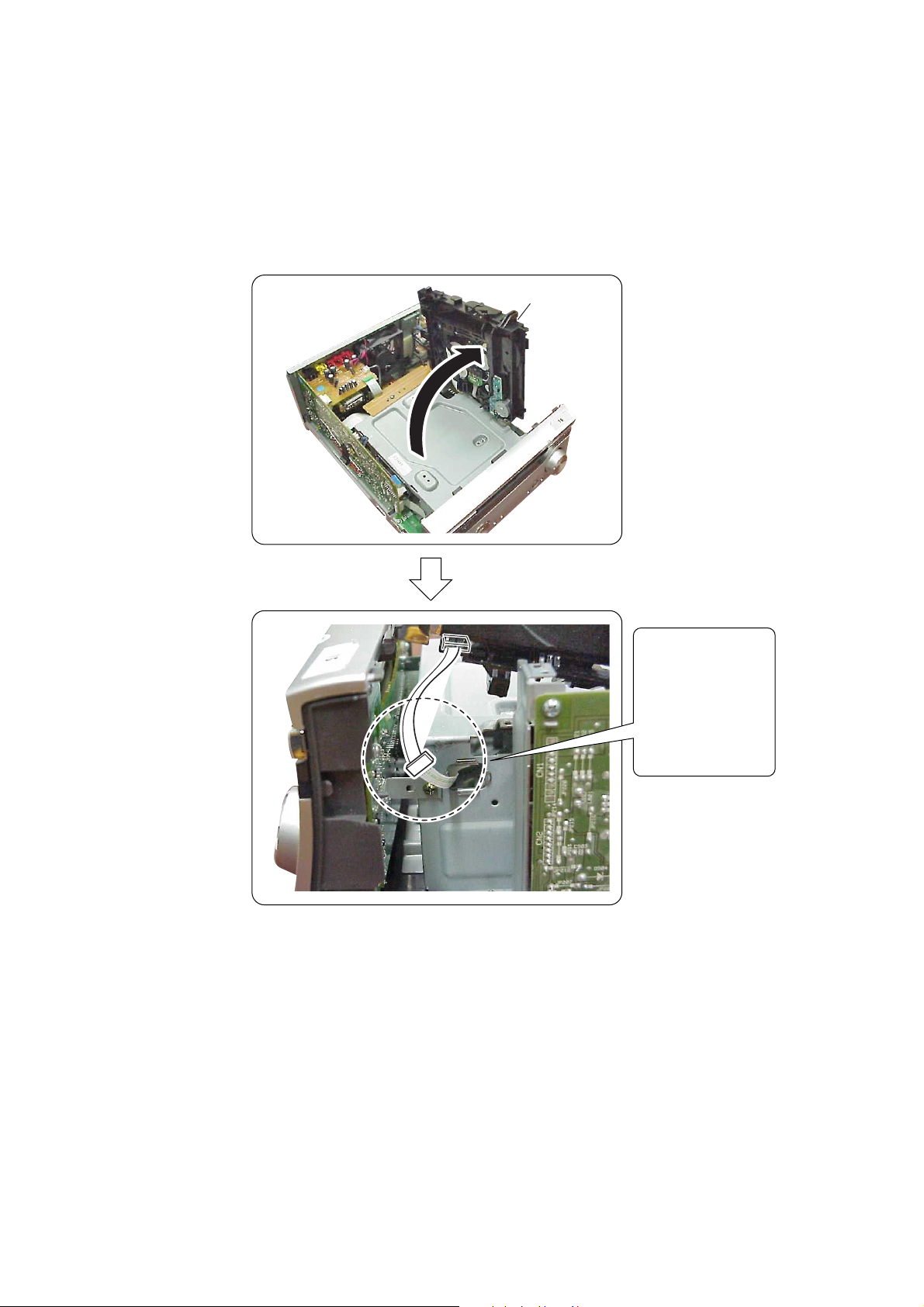
• REGULATOR board service position
HCD-WS2D
REGULATOR board
S-MASTER
BOARD
CN700
DMB10 BOARD
CN106
MAIN board
CN313
CN305
To check the soldering side of
the REGULATOR board, remove
the REGULATOR board and
MAIN boards.
It becames a resolution with
MAIN board.
CN302
MAIN BOARD
Extension cable :
J-2501-102-A
(1mm / 13pin / L300)
Extension cable :
J-2501-011-B
(1.25mm / 19pin / L300)
In such a case, the
extension cables
became necessary.
MAIN board
REGULATOR
board
5
Page 6

HCD-WS2D
• DMB10 board service position
DMB10 board
Remove the DMB10 board once.
Then create the service position.
VIDEO BOARD
Extension cable :
J-2501-102-A
(1mm / 13pin / L300)
CN100
CN313
CN302
MAIN BOARD
In such a case, the
extension cables
became necessary.
DMB10 board
Extension cable :
J-2501-244-A
(1mm / 21pin / L300)
6
Page 7

• S-MASTER board service position
HCD-WS2D
S-MASTER board
S-MASTER board
7
Page 8
HCD-WS2D
• Mechanism deck service position
Mechanism deck
In such a case, the
extension cables
became necessary.
Extension cable :
J-2501-239-A
(1mm / 5pin / L300)
8
Page 9
SECTION 2
GENERAL
List of button locations and reference pages
HCD-WS2D
This section is extracted
from instruction manual.
How to use this page
Use this page to find the location of buttons and other
parts of the system that are mentioned in the text.
Main unit
ALPHABETICAL ORDER
A – R S – Z
BASS/TREBLE 8 (45)
DIMMER qj (49)
Disc tray 2 (13)
DISPLAY qg (49, 53)
Display window 9
DSGX 6 (45)
DVD qf (10, 13, 35)
Headphones jack qd
PRESET +/– qs (43)
PROGRESSIVE 0 (35)
Remote sensor 4
SA-CD/CD qa (15)
SOUND FIELD 7 (45, 62)
TUNER AM qf (42, 43)
TUNER FM qf (42, 43)
TIME/TEXT qh (44, 50, 51)
VIDEO/SAT qf (56)
VOLUME control 5
Illustration number
SA-CD/CD
RR
Name of button/part Reference page
BUTTON DESCRIPTIONS
?/1 (power) 1 (9, 43, 62)
Z (open/close) 3 (13)
H (play) qs (13, 40)
X (pause) qs (10, 14)
x (stop) qs (14, 37, 62)
./> (go back/go forward)
qs (12, 14, 45)
r
qa (15)
9
Page 10

HCD-WS2D
Remote control
ALPHABETICAL ORDER
A – Q
ALBUM +/– wf (14)
ANGLE 5 (41)
AUDIO 4 (30, 46)
CLEAR es (16, 17, 19, 24, 27)
DISC SKIP
DISPLAY qj (49, 53)
ENTER qs (11, 12, 16, 17, 18, 19,
20, 23, 25, 27, 28, 31, 32, 37,
42, 43, 48)
FM MODE ws (44)
FUNCTION +/– 2 (13, 35, 42,
43)
KARAOKE MODE qg (46)
KARAOKE PON qh (47)
MENU 6 (19, 23, 25)
Number buttons
33, 37, 43, 54)
PICTURE NAVI 3 (24, 28)
PRESET + wh (43)
PRESET – e; (43)
1)
w;
2)
qf (19, 20, 27,
R – Z
REPEAT ws (18)
SLEEP qk (48)
SOUND FIELD wa (45)
SUBTITLE wd (41)
THEATRE SYNC ql (54)
TIMER MENU eg (11, 48)
TIME/TEXT ef (44, 50, 51)
TOP MENU qd (19)
TUNING + 9 (42, 44)
TUNING – qa (42, 44)
TV wk (54)
TV CH + wh (54)
TV CH – e; (54)
TV/VIDEO qk (54)
TV VOL +/–
VOLUME +/–
2)
7 (54)
2)
7 (48)
BUTTON DESCRIPTIONS
?/1 (power) 1 (9, 48)
TV ?/1 1 (54)
REPLAY/ADVANCE
8 (14)
c STEP/STEP C 8 (14)
SLOW y 9 (14)
M (fast forward) 9 (14)
X (pause) q; (14)
SLOW qa (14)
m (rewind) qa (14)
M/m/</, qs (11, 17, 31, 48)
DISPLAY wg (12, 17, 31, 46,
53)
> (go forward) wh (14, 45)
x (stop) wj (14, 37)
H (play)
. (go back) e; (12, 14, 45)
O RETURN ea (20)
-/-- es
KEY CONTROL
1)
The DISC SKIP button is not
available for this model.
2)
The H, number 5 and
VOLUME + (TV VOL +)
buttons have tactile dots. Use
the tactile dots as referenc es
when op erating the system.
2)
wl (13, 40)
#/2
ed (47)
Setting the clock
Use buttons on the remote for the operation.
1
Press ?/1 to turn on the system.
2
Press TIMER MENU.
3
Press M or m repeatedly to set the hour.
4
Press ENTER.
5
Press M or m repeatedly to set the
minute.
6
Press ENTER.
The clock starts wo rking.
To adjust the clock
1
Press TIMER MENU.
2
Press M or m to select “CLOCK SET?”, then
press ENTER.
3
Do the same procedures as step 3 to 6
above.
Notes
The clock settings are canceled when you disconnect
the power cord or if a power failure occurs.
You cannot set the clock in Power Saving Mode
(page 49).
10
Page 11

3-1. DISASSEMBLY FLOW
•This set can be disassembled in the order shown below.
•The dotted square with arrow (
) are completed.
(
SET
) prompts you to move to the next job when all of the works within the dotted square
HCD-WS2D
SECTION 3
DISASSEMBLY
3-2.CASE, FRONT PANEL SECTION
3-3.DISPLAY BOARD,
FUNCTION BOARD
(Page 13)
(Page 12)
3-4.VIDEO BOARD,
TUNER,DC FAN
(Page 13)
3-5.REGULATOR BOARD,
DVD MECHANISM DECK
(CDM85-DVBU102)
(Page 14)
3-6.MAIN BOARD,
SWITCHING REGULATOR,
HEADPHONE BOARD
(Page 14)
3-9.TRAY
(Page 16)
3-8.S-MASTER BOARD
3-7.DMB10 BOARD
(Page 15)(Page 15)
3-10.BELT, MS-203 BOARD
(Page 17)
3-12.OPTICAL PICK-UP
(KHM-310CAA/C2NP)
(Page 18)
3-11.BASE UNIT
(Page 18)
11
Page 12

HCD-WS2D
)
Note: Follow the disassembly procedure in the numerical order given.
3-2. CASE, FRONT PANEL SECTION
1
Push down the F spring in the
arrow direction and release
the claw.
three claws
2
Insert your hand from the rear and
push up the front of case as shown.
qs
front panel section
9
screw
(+BVTP 3
qa
three
(+BVTP 3
×
8)
screws
Be careful not to give scar on this part.
4
screw
(case 3 TP2
6
0
screw
(+BVTP 3
8
screw
×
8)
(+BV3)(3-CR)
×
8)
7
wire (flat type)
(17 core)
(CN315)
case
3
screw
(case 3 TP2)
5
three
screws
(+BVTP 3
×
8)
12
Page 13
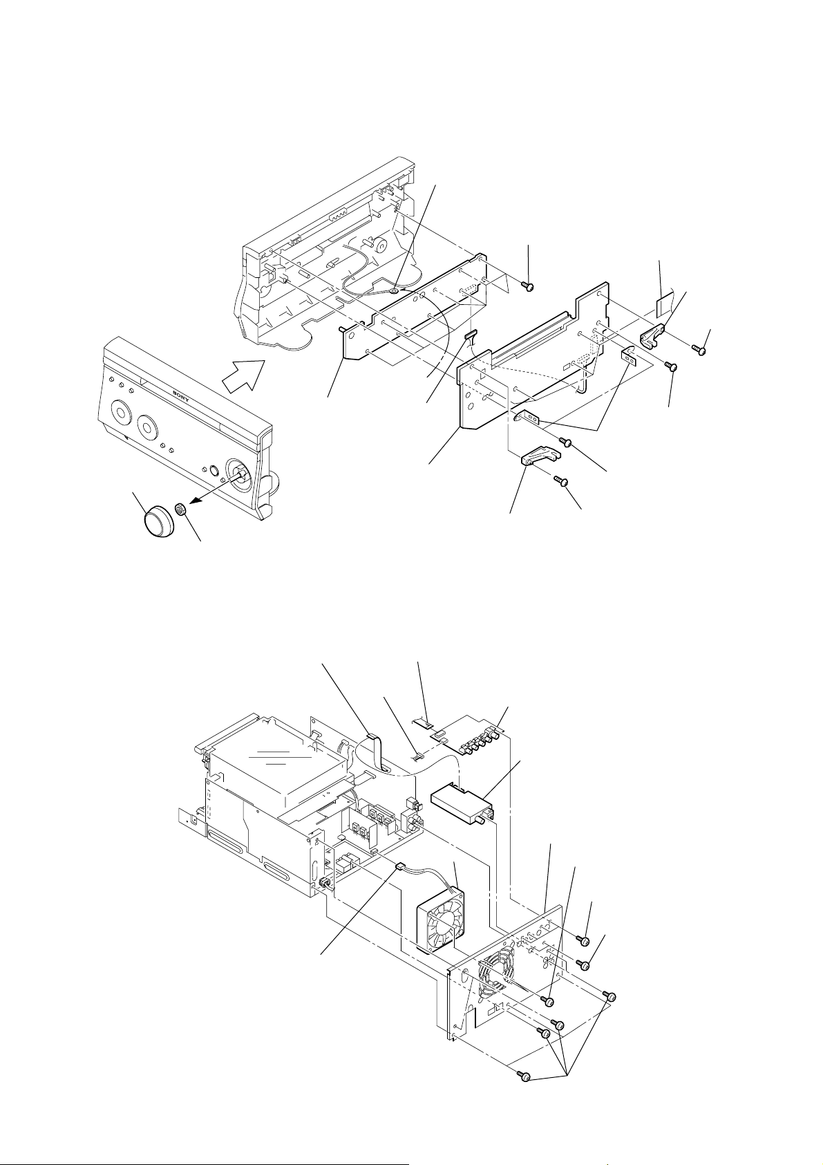
3-3. DISPLAY BOARD, FUNCTION BOARD
qa
DISPLAY
board
4
two
brackets (FL)
qg
FUNCTION
board
1
knob (vol)
2
nut
5
t
apping screw
(+BVTP 2.6
×
10)
7
t
apping screw
(+BVTP 2.6
×
10)
9
five t
apping screws
(+BVTP 2.6
×
8)
6
fixing CDM R
8
fixing CDM L
3
two t
apping screws
(+BVTP 2.6
×
8)
qs
nine t
apping screw
(+BVTP 2.6
×
8)
qd
earth wire
q;
wire (flat type)
(17 core)
(CN001)
qf
connector
(CN003)
HCD-WS2D
3-4. VIDEO BOARD, TUNER, DC FAN
6
wire (flat type)
(11 core) (CN311)
qa
(CN211)
3
connector
(CN101)
connector
2
wire (flat type)
(13 core) (CN100)
qs
DC fan
4
VIDEO board
7
tuner
q;
back panel
8
two screws
(+BVTP 3 × 8)
1
four screws
(+BVTP 3 × 8)
5
two screws
(+BVTP 3 × 8)
9
eight screws
(+BVTP 3 × 8)
13
Page 14

HCD-WS2D
3-5. REGULATOR BOARD, DVD MECHANISM DECK (CDM85-DVBU102)
8
loading panel
4
spring (loading panel)
5
HIMERON sheet
9
DVD mechanism deck
(CDM85-DVBU102)
6
wire (flat type)
(7 core) (CN202)
7
connector
(CN201)
2
cover
three claws
1
two
(+BVTP 3
screws
×
8)
3
three
(+BVTP 3
screws
×
8)
8
wire (flat type)
(24 core) (CN101)
qh
connector
(CN204)
qj
connector
(CN301)
qg
connector
(CN203)
qf
(CN201)
0
connector
screw
(+BV3 )
qd
three
screws
(+BV3 )
qk
REGULATOR board
3
panel comb
board
3-6. MAIN BOARD, SWITCHING REGULATOR, HEADPHONE BOARD
4
wire (flat type)
(19 core) (CN305)
6
5
screw
(+BVTP 3
MAIN board
×
8)
qk
bracket (CDM)
3
wire (flat type)
(21 core) (CN302)
qh
three
screws
(+BV3)(3-CR)
qj
clip coating
qs
bracket (SWA)
0
screw
(+BV 3)
qa
(CN215)
9
bracket (SWB)
qs
SPEAKER OUT board
connector
qf
cord bushing (2104)
qd
power cord
14
1
screw
(+BVTP 3
2
HEADPHONE
×
8)
board
qa
wire holder
7
connector
(CN1)
9
SW cover
qg
switching regulator
8
four
(+BVTP 3
screws
×
8)
Page 15

3-7. DMB10 BOARD
2
wire (flat type)
(7 core) (CN202)
1
wire (flat type)
(13 core) (CN106)
6
four
screws (3CR)
3
connector
(CN103)
4
connector
(CN401)
7
DMB10 board
5
connector
(CN101)
HCD-WS2D
3-8. S-MASTER BOARD
2
s-master
heat sink
3
four
(+BV 3)
screws
1
two
screws
(+BVTP 3
4
sheet radiation
5
×
12)
S-MASTER board
15
Page 16

HCD-WS2D
3-9. TRAY
1
Move the chuck cam
in the direction of the arrow.
bottom side
2
4
two claws
3
5
tray
16
Page 17

3-10. BELT, MS-203 BOARD
2
chuck cam
3
HCD-WS2D
belt
6
DC motor
1
two claws
7
MS-203 board
5
three claws
4
screw
(M 1.7
×
2.5)
17
Page 18

HCD-WS2D
3-11. BASE UNIT
2
chuck cam
1
two claws
3
two claws
3-12. OPTICAL PICK-UP (KHM-310CAA/C2NP)
3
four insulator screws
2
loading base
4
base unit
4
two insulators
18
bu holder
1
two claws
5
two insulators
6
optical pick-up
(KHM-310CAA/C2NP)
Page 19

SECTION 4
TEST MODE
HCD-WS2D
Note 1:Regarding the notification symbol “R”
Because the number of the operating buttons of this product
are limited, some operations require use of the operating buttons
of the remote commander.When a specific operation requires
use of the operating buttons of the remote commander, “R” is
added to the specific operating procedure in this manual.
Example MENU/NO “R” The MENU/NO button of remote
commander.
Note 2:Incorrect operations may be performed if the test mode is not
entered properly.
In this case, press the ?/1 button to turn the power off, and
retry to enter the test mode.
1. Cold Reset
• The cold reset clears all data including preset data stored in
the RAM to initial conditions. Execute this mode when
returning the set to the customers.
Procedure:
1. Press the ?/1 button to turn the power on.
2. Press three buttons x , [SOUND FIELD] and ?/1 simulta-
neously.
3. When this button is operated, display as “COLD RESET” for
a while and all of the settings are reset.
2. Panel Test Mode
•This mode is used to check the software version, LCD, LED
and keyboard.
Procedure:
1. Press the ?/1 button to turn on the power.
2. Press three bottons x , [PROGRESSIVE] and [TUNER AM]
simultaneously.
3. When the panel test mode is activated, all segments are turned
on.
2-1. V ersion T est Mode
Procedure:
1. When the panal test mode is activated, press the
PRESET –
displyed, the version test mode is activated.
2. Whenever press the PRESET – . button, the version is
displayed in order of CE2, MC, SYS, UI, DVD, ST, TA, TM
and WDS2D.
3. Press the PRESET > + button and the date of the softw are
production is displayed.
4. Press the PRESET > + button again and the version is
displayed.
5. To exit from this mode, press three buttons x ,
[PROGRESSIVE] and [TUNER AM] simultaneously.
2-2. Key Test Mode
Procedure:
1. When the panel test mode is activated, press the [DSGX] button,
to select the key test mode. In the key check mode, the
fluorecent indicator displays “K 0 V0”. Each time a b utton is
pressed, “K” value increases. However, once a button is
pressed, it is no longer taken into account. When all keys are
pressed correctly, “K18 V0” is displayed.
2. To exit from this mode, press three buttons
[PROGRESSIVE] and [TUNER AM] simultaneously.
.
button and the message “WDS2D” is
x
,
3. Common Test
Procedure:
1. Press the ?/1 button to turn the power on.
2. To enter the common test mode, press three buttons x , the
[PROGRESSIVE] and [TIME/TEXT] simultaneously.
3. To exit from this mode, press the ?/1 button.
3-1. AMP Test
1. When the common test mode is activated, each time press the
[BASS/TREBLE] button, the message “EQ LVL MAX”, “EQ
LVL MIN”, “EQ LVL FLAT” is displayed in this order.
2. The message “VOLUME MAX” is displayed, when press the
[VOLUME +] button. The message “VOLUME MIN” is displayed, when press the VOLUME – button.
3. To exit from this mode, press the ?/1 button to turn off the
main power.
4. Function Change
Procedure:
1. Press the ?/1 button to turn the power on.
2. Press the [FUNCTION] button to the function “VIDEO”.
3. Press the [VIDEO/SAT] button and the ?/1 button simulta-
neously, and the display changes to “VIDEO” or “SAT”.
4. To exit from this mode, press the ?/1 button.
5. Disc Tray Lock
The disc tray lock function for the antitheft of an demonstration
disc in the store is equipped.
Setting Procedure :
1. Press the ?/1 button to turn the set on.
2. Press the [FUNCTION] button to set DVD function.
3. Insert a disc.
4. Press the x button and the A button simultaneously for f ive
seconds.
5. The message “LOCKED” is displayed and the tray is locked.
Releasing Procedure :
1. Press the x button and the A button simultaneously for fi ve
seconds again.
2. The message “UNLOCKED” is displayed and the tray is
unlocked.
Note: When “LOCKED” is displayed, the slot lock is not released by
turning power on/off with the ?/1 button.
6. AM Step Change
•A step of AM channels can be changed over between 9 kHz
and 10 kHz.
Procedure:
1. Press ?/1 button to turn the set ON.
2. Select the function “TUNER”, and press the [TUNER AM]
button.
3. Press ?/1 button to turn the set OFF.
4. Press x and ?/1 buttons simultaneously , and the display of
fluorescent indicator tube changes to “ AM 9 k STEP” or “ AM
10 k STEP”, and thus the channel step is changed over.
19
Page 20

HCD-WS2D
DVD SECTION
4-1. GENERAL DESCRIPTION
The Mirror Time and IOP measurement allows you to make
diagnosis and adjustment simply by using the remote commander
and monitor TV. The instructions, diagnosis results, etc. are given
on the on screen display (OSD).
The Mirror Time and IOP measurement is required is such events
where servicing a DVD-Player includes changing the Base Unit
(BU). For each new BU to be used with a certain MV-044 board,
Mirror Time and IOP measurement need to be carried out.
4-2. STARTING TEST MODE
Press three buttons x , A and VOLUME + simultaneously
with the DVD player in standby mode.
The Test Mode starts, then the menu shown below will be
displayed on the TV screen.
Remocon Diagnosis Menu
0. External Chip Check
1. Servo Parameter Check
2. Drive Manual Operation
3. Emergency History
4. Version Information
5. Video Level Adjustment
4-4. MIRROR TIME ADJUSTMENT
To enter Mirror Time Adjustment, press 5 “R” button on the remote
commander. The screen will appear as below.
MIRR time Adjust Menu
1. CD MIRR time Check:
2. DVD MIRR time Check:
3. Threshold:
4. Save to EEPROM
5. Default set MIRR time
[Open] Tray open [Close] Tray close
[0] Return to previous menu
There are five main commands in the Mirr time Adjust menu as
shown in the figure above. The functions of each command are
described in the following page.
1. CD MIRR time Check
This command checks the Mirror time value for CD disc.
2. DVD MIRR time Check
This command checks the Mirror time value for DVD disc.
3. Threshold
This command displays the threshold value between CD and DVD
mirror time.
Model Name : WDS2D_XX
IF-con : V
Syscon : Ver.
er. xx.xx (xxxx)
x.xxx
The menu above is the Remocon Diagnosis Menu screen which
consists of six main function. At the bottom of the menu screen,
the model name and IF-con version. To enter Mirror Time
Adjustment menu, press button 2 “R” on the remote commander
to enter Drive Manual Operation menu. To exit from the Test Mode,
press the power button on the remote commander.
4-3. DRIVE MANUAL OPERATION
The Drive Manual Operation menu consists of five main
function. By pressing 2 “R” button on the remote commander in
the Remocon Diagnosis Menu, the screen will appear as below.
Drive Manual Operation
1. Servo Control
2. Track/Layer Jump
3. Manual Adjustment
4. Mecha t est mode
5. MIRR time Adjust
0. Return to Top Menu
4. Save to EEPROM
This command saves an adjusted mirror time value to the EEPR OM.
5. Default set MIRR time
This command will set CD and DVD mirror time to firmware def ault
value.
[Open] / [Close]
Pressing the A button controls the tray for disc change
during mirror time adjustment.
[0] Return to previous menu
Press 0 “R” button to return to previous menu.
4-4-1. EXECUTING MIRROR TIME ADJUSTMENT
In order to execute mirror time adjustment, the following standard
procedures must be followed.
(1) In standby mode, press three buttons x , A and V OLUME
+ simultaneously.
(2) Select “2. Drive Manual Operation”.
Remocon Diagnosis Menu
0. External Chip Check
1. Servo Parameter Check
2. Drive Manual Operation
3. Emergency History Check
4. Version information
5. Video Level Adjustment
20
Model : WDS2D_xx
IF-con : Ver. xx.xx (xxxx)
Syscon : Ver. x.xxx
Page 21

HCD-WS2D
(3) Select “5. MIRR time Adjust”.
Drive Manual Operation
1. Servo Control
2. Track/Layer Jump
3. Manual Adjustment
4. Mecha test mode
5. MIRR time Adjust
0. Return to Top Menu
(4) Select “5. Default set MIRR time”.
MIRR time Adjust Menu
1. CD MIRR time Check:
2. DVD MIRR time Check:
3. Threshold:
4. Save to EEPROM:
5. Default set MIRR time:
[Open] Tray open [Close] Tray close
[0] Return to previous menu
(5) Select “3. Threshold”.
(6) Confirm the number. If it is 75, go to next step. If it is any
other value, return to step 4.
MIRR time Adjust Menu
(14) Confirm the same values are displayed. If it is not same,
return to step 7.
MIRR time Adjust Menu
1. CD MIRR time Check:
2. DVD MIRR time Check: XX XX
3. Threshold:
4. Save to EEPROM:
5. Default set MIRR time:
[Open] Tray open [close] Tray close
[0] Return to previous menu
(15) Push A button to eject tray.
(16) Take out HLX-504 and insert Test Disc YEDS-18 into
tray.
(17) Push A button to close tray.
(18) Push “1. CD MIRR time check”.
(19) Wait for HEX number to display.
(20) Confirm the number, if YY is 5A ~ E8, proceed with next
step. If no, return to 15.
MIRR time Adjust Menu
1. CD MIRR time Check:
2. DVD MIRR time Check:
3. Threshold: 75
4. Save to EEPROM:
5. Default set MIRR time:
[Open] Tray open [Close] Tray close
[0] Return to previous menu
(7) Push A button to eject tray.
(8) Insert Test Disc HLX-504 into tray.
(9) Push A button to close tray.
(10) Push “2. DVD MIRR time Check”.
(11) Wait for HEX number to display.
(12) Confirm the number, if XX is 28 ~ 70, proceed with next
step. If no, return to 8.
MIRR time Adjust Menu
1. CD MIRR time Check:
2. DVD MIRR time Check: xx xx
3. Thereshold:
4. Save to EEPROM:
5. Default set MIRR time:
[Open] tray open [close] Tray close
[0] Return to previous menu
1. CD MIRR time Check: yy YY
2. DVD MIRR time Check: XX XX
3. Threshold:
4. Save to EEPROM:
5. Default set MIRR time:
[Open] Tray open [close] Tray close
[0] Return to previous menu
(21) Push “4. Save to EEPROM”.
(22) Confirm the same values are displayed. If it is not the
same, return to step 15.
MIRR time Adjust Menu
1. CD MIRR time check: YY YY
2. DVD MIRR time check: XX XX
3. Threshold:
4. Save to EEPROM:
5. Default set MIRR time:
[Open] Tray open [close] Tray close
[0] Return to previous menu
(23) Push A button to eject tray.
(24) Remove Test Disc YEDS-18 from tray.
(25) Push A button to close tray.
(26) Press 0 “R” button to the Drive Manual Operation menu.
(13) Push “4. Save to EEPROM”.
(27) Press 0 “R” button to return to the Remocon Diagnosis
Menu.
(28) Press the ?/1 button to switch OFF set.
21
Page 22

HCD-WS2D
4-5. EXECUTING IOP MEASUREMENT
In order to execute mirror time adjustment, the following standard
procedures must be followed.
(1) In standby mode, press three buttons x , A and VOLUME
+ simultaneously.
Remocon Diagnosis Menu
0. External Chip Check
1. Servo Parameter Check
2. Drive Manual Operation
3. Emergency History Check
4. Version information
5. Video Level Adjustment
Model : WDS2D XX
IF-con Ver : XX.XX (XXXX)
Syscon Ver : X.XX
(2) Select “2. Drive Manual Operation” by pressing the 2 “R”
button on the remote commander. The screen will appear as
below.
Drive Manual Operation
1. Servo Control
2. Track/Layer Jump
3. Manual Adjustment
4. Tray Aging Mode
5. MIRR time adjust
0. Return to top Menu
(5) Wait until a hexadecimal number appear.
Manual Adjust
1. Track Balance Adjust:
2. Track Gain Adjust:
3. Focus Balance Adjust:
4. Focus Gain Adjust:
5. Eq Boost Adjust:
6. Iop. ED 9E:
7. TRV. Level:
8. S curve(FE) Level:
9. RFL(PI) Level:
0. MIRR Time:
Change Value
[0] Return to previous menu
(6) Convert each data from hexadecimal to decimal using
conversion table.
(7) Substract between these two values.
(8) If the remainder is smaller than 93 (decimal), then it is
OK. However if the value is higher than 93, then the BU
is defective and need to be change.
(9) Press RETURN “R” button to return back to previous menu.
(10) Press 0 “R” button to return to Top Menu and power OFF
the DVD Player.
(3) Select “3. Manual Adjustment” by pressing the 3 “R” b utton
on the remote commander. The screen will appear as below.
Manual Adjust
1. Track Balance Adjust:
2. Track Gain Adjust:
3. Focus Balance Adjust:
4. Focus Gain Adjust:
5. Eg boost Adjust:
6. Iop:
7. TRV. Level:
8. S curve(FE) Level:
9. RFL(PI) Level:
0. MIRR Time:
o O Change Value
[RETURN] Return to previous menu
(4) Select Iop by pressing 6 “R” button on the remote commander .
22
Page 23

SECTION 5
DIAGRAMS
THIS NOTE IS COMMON FOR PRINTED WIRING BOARDS AND SCHEMATIC DIAGRAMS.
(In addition to this, the necessary note is printed in each block.)
For Schematic Diagrams.
Note:
• All capacitors are in µF unless otherwise noted. (p: pF)
50 WV or less are not indicated except f or electrolytics and
tantalums.
• All resistors are in Ω and 1/
specified.
• f : internal component.
• C : panel designation.
Note: The components identified by mark 0 or dotted
line with mark 0 are critical for safety.
Replace only with part number specified.
• A : B+ Line.
• B : B– Line.
•Voltages and wavef orms are dc with respect to ground under no-signal (detuned) conditions.
•Voltages and waveforms are dc with respect to ground in
service mode.
•Waveforms are taken with a oscilloscope.
Voltage variations may be noted due to normal production
tolerances.
no mark : DVD STOP
•Voltages are taken with VOM (Input impedance 10 MΩ).
• Circled numbers refer to waveforms.
• Signal path.
J : CD PLAY
c : DVD PLAY
I : SACD PLAY
L : VIDEO
E : Y
a : CHROMA
r : COMPONENT VIDEO
q : R, G, B
f : AUDIO (TUNER)
h : AUDIO (ANALOG)
i : AUDIO (DIGITAL)
•Abbreviation
E3 : 240 V AC Area in E model.
HK : Hong Kong model.
RU : Russian model.
SP6 : Singapore and Malaysia models.
4
W or less unless otherwise
For Printed Wiring Boards.
Note:
• X : parts extracted from the component side.
• a : Through hole.
• : Pattern from the side which enables seeing.
(The other layers' patterns are not indicated.)
Caution:
Pattern face side: Parts on the pattern face side seen from
(SIDE A) the pattern face are indicated.
Parts face side: Parts on the parts face side seen from
(SIDE B) the parts face are indicated.
• Indication of transistor.
C
Q
B
E
B
These are omitted.
Q
CE
These are omitted.
• Circuit Boards Location
DISPLAY board
HEADPHONE board
MS-203 board
FUNCTION board
HCD-WS2D
VIDEO board
MAIN board
DMB10 board
DROP TEST board
SPEAKER OUT board
REGULATOR board
SWITCHING REGULATOR
S-MASTER board
HCD-WS2D
2323
Page 24

HCD-WS2D
5-1. BLOCK DIAGRAM – RF/SERVO SECTION –
RFMON
RF
DETECTOR
OPTICAL PICK-UP
BLOCK
(KHM-310CAA/C2NP)
VC
LASER
DIODE
(FOR CD)
LASER
DIODE
(FOR DVD)
CD LD
PD
DVD LD
VR650
VR780
DVDRFIP
6
OSP
252 253
A
B
C
D
F
E
B
A
C
D
SW+3.3V
Q102 (1/2)
AUTOMATIC POWER
CONTROL (FOR CD)
Q102 (2/2)
AUTOMATIC POWER
CONTROL (FOR DVD)
Q101, Q103
VOLUME CONTROL
A
B
D
C
2
3
4
5
19
18
8
9
10
11
176
29
23
20
21
22
187
DVDA
DVDB
DVDC
DVDD
TPI
TNI
NA
NB
MD
MC
LI M SW
V20
LD01
MD12
MD11
LD02
MSW
OSN
IC102 (1/3)
CD/DVD RF AMP,
FOCUS/TRACKING ERROR AMP
DVD SYSTEM PROCESSOR
DIGITAL SERVO PROCESSOR
V2REF0
RXD
TXD
XTALO
XTALI
PRST
IFCK
MREQ
IFSDO
IFSDI
XIFCS
28
106
107
228
229
110
99
114
98
101
100
X101
27MH
Z
V2REF0
RXD
TXD
for TEST
34
P_ID_IO_SYSRST
PI_DVD_SCK
33
25
P_I_MREQ
32
P_I_DVD_SI
31
P_O_DVD_SO
26
P_I_DVD_XIFCS
2AXIS
DEVICE
FOCUS/
TRACKING
COIL
VCC
FCS+
FCS–
TRK+
TRK–
M2
(SLED)
M1
(SPINDLE)
M203
LOADING MOTOR
MM
MM
MM
+3.3V
SP+
SP–
FOCUS/TRACKING COIL DRIVER,
SPINDLE, SLED MOTOR DRIVER
42
41
36 48
37 1
35 3
34 4
32
31
SL–
30
SL+
29
27
28
47
46
24
25
IC201
BUFFER
FOCUS COIL
DRIVE
TRACKING COIL
DRIVE
SLED MOTOR
DRIVE
SPINDLE MOTOR
DRIVE
BUFFER
LOADING MOTOR
DRIVER
TSD
43
10
13
40
45
19
20
22
21
15
16
17
VREF0
FOO
TRO
FMO
DMO
TROPENPWM
FWD
REV
OCSW
CKSW
VREF0
FMO
FOO
DMO
TRO
38
FMO
42
FOO
37
DND
41
TRO
V REFO
30
246
V REFO
40
IOPMON
47
SPFG
184
MUTE123
183
MUTE
181
TSDM
TROPENPWM
39
FWD
186
REV
185
OCSW
177
CKSW
179
IFBSY
KRMOD
105
207
P_VIDEO_MUTE
28
P_O_DVD_BUSY
27
P_I_KRMOD
IC401 (1/3)
SYSTEM
CONTROLLER
19
P_DVD_I_MTK_SLOT_IN
23
VMUTE
SECTION
(Page 25)
• Signal Path
A
VIDEO
: CD PLAY
: DVD PLAY
:SACD PLAY
HCD-WS2D
2424
Page 25

5-2. BLOCK DIAGRAM – VIDEO SECTION –
Y
194
YUV1
C
196
YUV2
V
198
YUV3
200
YUV4
202
YUV5
203
YUV6
171
WODE
Y/G
HCD-WS2D
IC100
VIDEO AMP, 75Ω DRIVER
6
YIN
2
CIN
4
CVBSIN
10
CYIN
Cb
Cr
12
CBIN
14
CRIN
25
SI
MUTE1
3
139
YOUT
COUT
CVBSOUT
CYOUT
CBOUT
CROUT
MUTE2
21
26
21
43
J100
S VIDEO OUT
• Signal Path
VOUT
23
J102
VIDEO OUT
: VIDEO
: Y
CYOUT
20
CBOUT
18
CROUT
16
Y,P
CB,P
C
B
R
R
J103
COMPONENT
VIDEO OUT
VMUTE
: CHROMA
: COMPONENT VIDEO
: R, G, B
RF/SERVO
A
SECTION
(Page 24)
SCL
SDA
B
SPEAKER
SECTION
(Page 26)
SCL
102
103
6 5
SCL
IC103
EEPROM
SDA
SPA
IC102(2/3)
DVD SYSTEM PROCESSOR
AD0 – AD7
81-84,86-88,91
HD0 – HD7 A0 – A21
DATA & ADDRESS BUS
DATA & ADDRESS BUS
HD0 – HD7
29,31,33,35,38,40,42,44 25-16,10-1, 48
DQ0 – DQ7
HIGHA0-7
IOA0-7, IOA18-IOA20
A16, A17
53-61, 67-72, 74-76,
78, 89, 92, 93
A0
A0 – A19DQ15/A-1
IC101
FLASH ROM
188
DSEL
A1-A21
XRD
XROMCS
2645
28OE11
CE
IOCS
77
79
XRD
XROMCS
XWR
WE
IOWR
IOUE
66
XWR
2,4,5,7,8,10,11,13,42,44,45,47,48,50,51,53
RD0 – RD15
125-123, 121, 120, 118,
117, 115, 135, 133-128, 126
RD0 – RD15
RA0 – RA11
146, 147, 149-151,
158-160, 162, 164-166
22-26,
29-35
RA0 – RA11
IC104
SDRAM
RCLK
RCS
RWE
MRAS
BA0
BA1
143
20
142
145 156 113 137 157
38
19
21
BS0
BS1
DRCLK
138
RCS
CAS
140
139
16
18
17
CAS
RAS
RWE
MDQM0
15
DQM0
MDQM1
39
DQM1
CKE
37
DRCKE
HCD-WS2D
2525
Page 26

HCD-WS2D
5-3. BLOCK DIAGRAM – SPEAKER SECTION –
IC102(3/3)
DVD SYSTEM PROCESSOR
225
VIDEO
AUDIO OUT
SPDIF
217
ASDATA0
ASDATA1
218
ASDATA2
219
ASDATA4
222
215
ACLK
214
ABCK
213
ALRCK
220
XRST
VIDEO SECTION
(Page 25)
FM/AM
TUNER UNIT
L CHFM IN
R CHAM IN
RDS CLK
RDS DATA
TUNED
DI
CLK
DO
CE
L
R
J301(1/2)
S055
CD/SACD
B
L-IN
R-IN
S044
S045
PROGRESSIVE
S056
14
15
16
13
10
9
17
8
19
20
AM
FM
DVD
PLAY
AMS+
AMS–
PAUSE
S054
DSGX
STOP
IC301
8-CH D/A CONVERTER
STDI1
STDI2
STDI3
STDI4
MCLK
BICK
LRCK
PDN
SCL
SDA
TIME/TEXT
S039
DIMMER
S052
BASS/TREBLE
S053
SOUND
FIELD
LOUT1– FL
1
LOUT1+
2
ROUT1+
48
47
ROUT1–
LOUT4+
38
LOUT4–
37
ROUT4+
33
32
ROUT4–
S043
S041
POWER
S040
DISPLAY
S042
CD OPEN
IC3711
L.P.F
2
3
5
6
3
2
5
6
IC3771
L.P.F
Q307,308
SURR/2ch STEREO
IC391
RESET
3 1
2
–
+
–
+
–
+
–
+
SELECT
1
7
1
7
Q391
FR
LT
RT
32.768KHz
X401
X402
5KHz
Q311-314
SIGNAL
SELECT
88
43
37
38
39
40
41
75
76
12
20
94
95
97
71
72
10
11
13
15
IC401(2/3)
SYSTEM CONTROLLER
P_VACS
SURR
ST TUNED
ST DIN
ST CLK
ST DOUT
ST CE
RDS CLK
RDS DATA
RESET
ACCUT
KEY_2
KEY_1
KEY_0
VOL A
VOL B
XC IN
XC OUT
X OUT
X IN
P_RECOUT_MUTING
P_SM_NSP_MUTING
AUDIO SELECTOR
SUR2 L RECA2
41
SUR1 R
42
INC2
38
INC1
5
39
INB2
4
INB1
37
IND2
IND1
6
RECB2
35
RECB1
8
CLOCK
22
DATA
21
P_AMPIC_CLK
P_AMPIC_DATA
P_HP_MUTING
P_HEADPHONE_IN
P_SM_DRV_RST
P_SM_SD
P_SM_OTW
P_ADC_RESET
SOFT_MUTE
PG_MUTE
P_SM_DATE
P_SM_CLK
P_SM_CS1
P_SM_INT
P_SM_ODF
IC301
70
69
61
42
60
54
55
56
59
57
68
67
1
2
52
58
53
RECA1
OUT2
OUT1
IC303
DIGITAL
OPTICAL OUT
36
7
25
18
A+9V
Q304
RIPPLE FILTER
2
3
5
6
Q310,368,369
MUTE
8
–
+
–
+
IC302
HP AMP
LT
1
RT
7
L-OUT
R-OUT
Q370,371
MUTE
HP SW
Q305,306
MUTE
HP R
HP L
J301(2/2)
L
R
VIDEO
AUDIO OUT
J066
i
• Signal Path
: AUDIO(TUNER)
: AUDIO(ANALOG)
: AUDIO(DIGITAL)
Q301
MUTE DRIVE
Q302
MUTE DRIVE
IC707
IC701
A/D CONVERTER
LIN
1
2
7
CLOCK GEN
2 4 1 3
49.152MHz
X702
RIN
PDWN
IC709
DOUT
BCK
LRCK
SCKI
12
11
10
15
IC703
24.576MHz GEN
CK Q
IC705
DATA CONVERTER
DATA
31
BCK
30
LRCK
29
XFSOIN
48
XFSIIN
36
NSPMUTE
18
SOFTMUTE
19
PGMUTE
20
SCDT
21
SCSHIFT
22
SCLATCH
23
INIT
27
OVF FLAGR
24
OVF FLAGL
25
OUTL1
OUTL2
OUTR1
OUTR2
/RST
/SD
/OTW
11
9
6
4
4
/RST
13
/SD
15
/OTW
2
BP
17
AP
4
13
15
2
17
POWER AMP
OUTB
OUTB
OUTA
OUTA
Q701
PROTECT
/RST
/SD
/OTW
BP
AP
IC708
POWER AMP
OUTB
OUTB
OUTA
OUTA
30
29
26
25
Q702,703
DC OFFSET
DETECT
Q752,753
DC OFFSET
DETECT
L-CH
SPEAKER
FAN CTRL
C
POWER
SECTION
(Page 27)
30
29
26
25
R-CH
SPEAKER
HCD-WS2D
2
S060
VOLUME ENCODER
1
3
2626
Page 27

5-4. BLOCK DIAGRAM – POWER SECTION –
30.5V
G+12V
A+5V
IC710
A+5V REG
HCD-WS2D
A+9V
Q011, Q012
D006
D+4V
FL001
FLOURESCENT INDICATOR
5
40
45
58
4
SEG1
39
SEG5
41
COM2
52
COM13
COM1
40
COM14
53
IC001
FL DRIVER
RESET
D+3.3V
1.8V
T001
DC/DC CONVERTER
TRANSFOTMER
D001-004
VP
Q202
OSC
–32V
63
DA
CP
62
CS
61
60
DVD M+9V
M+9V
AUDIO+9V
UNREG+10.5V
SW+5V
DVD A+5V
3.3V
3.3V
SW3.3V
1.8V REG
IC105
3.3V REG
IC107
3.3V REG
IC704
IC706
D3.3V REG
IC204
DVD M+9V REG
IC201
M9V REG
IC202
AUDIO +9V REG
IC205
SW +5V REG
IC206
SW3.3V REG
AC IN
UNREG+12V
POWER UNIT
UNREG+10.5V
EVER+4V
ON/OFF
EVER+4V
D385
IC041
REMOTE CONTROL
RECIVER
3
+3.3V
OUT
1.8V
RF1.8V
IC401(3/3)
SYSTEM CONTROLER
FAN DRIVE
47
48
49
5
DATA
7
D041
STANBY
2
CLK
6
CS
3
RESET
100
STANBY LED
4
SIRCS
P_O_DVD_POWER
STBY_RELAY
EVER+4V
D+4V
DVD_P_ON
ON/OFF
FAN DRV
IC106
1.8V REG
Q209,208
PWR CONT
SPEAKER
SECTION
(Page 26)
IC203
D+4V REG
c
FAN CTRL
Q271
Q272,273
Q274
DC FAN
HCD-WS2D
2727
Page 28

HCD-WS2D
5-5. PRINTED WIRING BOARD – DMB10 SECTION (SIDE A) –
H
VIDEO
BOARD
CN100
(Page 45)
• See page 23 for Circuit Boards Location. :Uses unleaded solder.
C3803
R3805
C3804
C3802
E
Q3801
R3804
C3805
AEP, UK, RU
E
2
1
R3803
R3788
R3787
C3784
C3783
R3785
R3786
R3782
R3784
C3781
R3782
R3781
IC103
C3777
C3773
R3775
R3782
R3778
R3777
C3774
R3776
R3774
R3772
C302
C3772
C3771
M
CN302
R3773
R3771
C306
MAIN
BOARD
CN302
(Page 36)
R3728
C3722
C3724
C3723
R3725
R3726
C3722
R3722
C3724
R3721
C3721
R3723
C305
R3653
C3701
20
21
C3718
R3718
C3711
R3712
R3776
R3718
R3717
C3774
R3716
C3712
R3713
R3711
R3651
R3802
C307
C3801
R3801
R319
IC103 (EEP ROM) can not be replaced individually.
✩
Replace it with DMB10 board assembly for service.
• Semiconductor
Location
Ref. No.
D1001 D-6
D3501 A-5
D3502 A-5
IC101 E-4
IC103 C-5
IC104 D-5
IC106 D-6
IC201 E-6
Q103 C-3
Q3801 B-5
Location
OPTICAL
PICK-UP
BLOCK
(KHM-310CAA/C2NP)
R243
CN202
C226
C225
IC101
R1545
IC102
IC104
1
5
IC106
F
R227
C223
R228
IC201
10
11
REGULATOR
BOARD
CN203
(Page 39)
for
TEST
HCD-WS2D
G
MS-203
BOARD
CN001
(Page 43)
A
MAIN
BOARD
CN313
(Page 36)
2828
Page 29

HCD-WS2D
5-6. PRINTED WIRING BOARD – DMB10 SECTION (SIDE B) –
• See page 23 for Circuit Boards Location. :Uses unleaded solder.
R3779
R3719
1
4
IC3711
C301
R314
C3702
R3729
8
5
48
1
IC301
13
IC3771
C3708
R3789
1
8
4
5
R1524
36
25
R3501
R1161
R1126
R1552
R1526
IC107
3
4
• Semiconductor
Location
R321
IC105 D-5
IC107 B-5
IC301 C-2
Ref. No.
R308
IC3711 B-2
IC3771 B-3
Q101 C-5
Q102 D-5
1
5
S
S
Location
R222
R1555
R236
R238
R2505
IC105
4
5
R239
E
E
3
1
R237
HCD-WS2D
2929
Page 30

HCD-WS2D
5-7. SCHEMATIC DIAGRAM – DMB10 SECTION (1/4) –
CN401
5P
JL4601
JL4602
JL4603 JL4604
JL4605 JL4606
JL4607 JL4608
JL4609 JL4610
40
FB402
FL401
0UH
0UH
C402
16V
47
FB404
0UH
FB403
FB401
FL403
0UH
0UH
C403
47
6.3V
FL402
EMI
0UH
FB406
0UH
FB405
0UH
31, 32, 33
31, 32, 33
33
R3781
R3783
2.2k
R3651
0
C301
ICT301
0
R3653
R3652
0
31
JL345
JL346
JL347
JL348
JL349
R314
JL344
100
JL343
0.01
IC301
AK4358VQ-L
JL3653
JL3652
JL3651
C305
0.47
C306
6.3V
100
C3771
1500p
R3803
10k
R3802
R3804
15k
C3801
6.3V
R3801
0
Q3801
2SC2712-YG
-TE85L
C3802
10
100
0
R3805
1k
C3805
47
4V
C3803
100
4V
C3804
47
6.3V
L.P.F
C3781
1500p
R3782
R3772
2.2k
R3771
2.2k
C3721
1500p
R3722
2.2k
L.P.F
R3721
2.2k
2.2k
C3701
0.1
R3784
5.6k
R3785
R3775
4.7k
R3774
5.6k
R3773
5.6k
R3724
5.6k
R3725
4.7k
5.6k
4.7k
R3723
5.6k
C3782
2200p
C3708
0.1
C3773
C3722
2200p
C3702
0.1
C3783
470p
470p
C3772
2200p
C3723
470p
R3787 R3788
1k
R3786
1k
0.1
C3707
R3776
1k
R3777
R3727
1k
R3726
1k
4.7k
C3784
470p
R3779
C3774
470p
R3778
1k 4.7k
R3728
4.7k
C3724
470p
R3789
IC3771
NJM3414AV(TE2)
1k
IC3711
NJM3414AV(TE2)
1k
R3729
CN302
R3501
1k
JL3501
0
JL3502
JL3503
JL3504
JL3505
JL3506
JL3507
JL3508
JL3509
JL3510
JL3511
JL3512
JL3513
JL3514
JL3515
JL3516
JL3517
17P
31
37
HCD-WS2D
C3714
R3719
31
R319
0
C307
100
C302
0.47
6.3V
R3712
2.2k
C3711 C3712
1500p 2200p
R3711
2.2k
4.7k
R3714
5.6k
R3713
5.6k
C3713
470p
R3716R3715
1k
R3717
1k
470p
R3718
4.7k
1k
D3501
1SS355TE-17
D3502
1SS355TE-17
3030
Page 31

HCD-WS2D
5-8. SCHEMATIC DIAGRAM – DMB10 SECTION (2/4) –
(Page 33)
R126
0
(Page 30, 32, 33)
(
KHM-
310CAA/
C2NP
(Page 33)
)
(Page 33)
(Page 32)
(Page 33)
(Page 33)
(Page 33)
TROPENPWM
CN101
FL101
0UH
24P
R101
100
CL106
C101
JL139
0.01
JL140
JL141
JL142
JL143
JL144
CL112
JL145
JL146
CL113
JL147
JL148
CL114
JL149
CL115
JL150
CL116
JL151
JL152
JL153
CL117
JL154
CL118
JL155
JL156
JL157
JL158
JL159
Q101
UM6K1N-TN
R108
ICT121
ICT123
R110
47k
R107
10k
CL107
ICT114
ICT115
ICT117
ICT118
TROPENPWM
ICT129
IC107
C192
TK11133CSCL-G
0.01
R116
1k
C117
10 16V
C115
0.1
C118
10 16V
C116
R117
0.1
47k
ICT127
R111
1M
100
R113
R112
R115
22
22
22
C105
47
6.3V
ICT124
R114
C106
R1129
100k
0.01
100k
R109
0
ICT126
RT1N241C-TP-1
22
22
22
C112
47
6.3V
121
R120
R
R118
Q102
QST8TR
• See page 55 for IC Pin Function Description. • See page 47 for Waveforms.
(Page 32)
R138
C193 C195
0.22
C114
0.1
C119
10
16V
Q103
R124
47k
R123
0
C113
0.01
C120
C121
C122
C123
C124
CL1501
ICT125
2p
100k
2
0.1
40
39
1
C
C132C130
0.10.1
ICT128
0.22
1
1
1
1
1
C125
0.1
C126
0.1
C196
0.0047
TROPENPWM
R133
3.3k
R134
3.3k
R135
3.3k
C127
0.01
C128
0.0015
CL105
JL101
JL130
JL167
JL102
JL127
JL132
JL133
CL101
JL135
CL104
CL108
CL109
CL110
JL136
k
15
C133
0.1
136
R
C1
1
.00
0.1
0
0.033
137
138
135
C
C
C
.1
0
0.1
0.1
1
141
C
JL103
C143
C146
C145
C147
0.047
.1
0
142
C
V
04
JL1
C149
0.1
C148
0.047
12p
16
150
JL105
C
JL106
10
152
C
k
0.001
750
151
141
C
R
DMB10 BOARD
(Page 30)
4
TA
A
D
AS
z
H
M
p
27
101
X
100k
142
R
T133
12
0
IC
R143
4
547
100
153
C
470
68
11
R
CXD9804R
156
14
4.7k
0.01
C
R1
R
0.1
154
C
IC102
(Page 30)
ST
XR
4.7k
7
4.7k
0
0
4
47
0
154
R
R151
47
49
53
155
47
15
160
1531
R
R1
R
R
R
1550
4.7k
R
548
.7k
1
166
4
R
JL
R
30
15
R
R1551
4.7k
C159
0.01
R1543
5
29
16
JL
10k
JL1
(3/4)
104
(Page 32)
D
O
IC
RM
M
K
4
52
1
R
0
6
52
1
0
.01
0
C161
0
2
R154
160
JL128
JL
7
C163
0.01
6
8
0
89
192
19
150
150
R
R1
1102
150
150
150
197
R1120
R195
R
R
ICT136
ICT134
JL113
CL120
JL161
JL162
0UH
150
R
R1121
0UH
R1125
0UH
R1124
0UH
R1123
0UH
R1122
0UH
R1101
2.2k
R1553
C170
0
0.01
R1161
C172
R1108
R1554
JL163
R1126
0
2.2k
C171
0.01
R1107
0.01
10k
R1109
4.7k
C173
0.01
C174
0.01
C175
0.01
C176
0.01
RB108
22
JL4701
JL4702
R4701
0
JL4703
JL4704
JL4705
JL4706
R4702
0
JL4707
JL4708
R4703
0
JL4709
JL4710
R4704
0
JL4711
JL4712
R4705
0
JL4713
R4706
0
R1103
10k
10k
R1104
10k
R1105
0
ICT1501
0
4.7k
R1555
R1111
0
RB104
0
RB103
0
RB111
0
ICT138
ICT109
ICT130
CN301
13P
R321
(Page 30, 32, 33)
0
R308
0
DMB10 BOARD
FWD
101
REV
CKSW
102
OCSW
(Page 33)
(4/4)
(Page 33)
(Page 33)
DMB10 BOARD
(4/4)
(Page 33)
H
VIDEO
BOARD
CN100
(Page 46)
HCD-WS2D
DMB10
BOARD
(1/4)
(Page 30)
100
ICT112
FL105
0UH
C129
10
16V
SCL
SDA
C131
2.2
1
C136
0.0
C144
0.01
13
T1
JL168
IC
C155
9
0.01
JL16
JL170
0
152
R
JL171
JL172
C158
0.01
C160
100
0.01
100
557
R164
1
161
100
R
R
JL164
RB113
C164
0.01
22
173
JL
0
1504
R
RB112
22
R196
C177
C162
47
0.01
6.3V
RB107
0
22
FL106
0UH
(Page 32)
(Page 32)
3131
Page 32

HCD-WS2D
5-9. SCHEMATIC DIAGRAM – DMB10 SECTION (3/4) –
IC101
*
MBM29DL32TF70-OBA4-0501GA(E3,HK,SP6)
MBM29DL32TF70-OBA4-0501CE(AEP,UK,RU)
IC101
*
(Page 31)
(Page 31)
IC103 (EEP ROM) can not be replaced individually.
✩
Replace it with DMB10 board assembly for service.
C181
0.1
RB106
47
C180
0.1
C191
0.1
A
MAIN
BOARD
CN313
(Page 38)
DMB10
BOARD
(4/4)
(Page 33)
103
OSCW1
MIC
VOICE 12
KRMOD
CN106
13
CN105
RB105
R104
0
R105
10k
R106
10k
R1546
3.3k
13P
6P
JL107
JL108
JL109
JL110
JL111
JL112
JL138
JL114
JL115
JL116
JL117
JL118
JL119
JL120
JL121
JL122
JL123
C102
0.01
R169
10k
R1133
R1134
ICT110
ICT111
0
IC106
PQ018EZ01ZP
0
FL104
0UH
R193
R191
1k
IC103
ICT104
ICT106
ICT102
R1546
3.3k
ICT107
ICT105
ICT101
R1150
R1152
3.3k
R1151
3.3k
3.3k
ICT103
0.001
C108
R1110
ICT137
FB111
0UH
FB112
0.001
C109
2.7k
R1502
FB113
FB114
FB115
0UH
0UH
0UH
0
0UH
BR24L64F-WE2
C167
0.01
1k
FL107
0UH
C178
47
4V
IC104
HY57V64162
0HGTP-HDR
ICT108
C184
0.01
C182 C188
0.22 0.22
IC105
TK11133CSCL-G
C189
0.33
R187
0
D1001
RB501V-40TE-17
C179
0.1
FL108C190
0UH47 6 . 3V
C187
47
4V
47
(Page 30, 31, 33)
(Page 31)
(Page 30, 31, 33)
HCD-WS2D
104
KRMOD
VOICE
DMB10
BOARD
(2/4)
(Page 31)
(Page 31)
3232
Page 33

5-10. SCHEMATIC DIAGRAM – DMB10 SECTION (4/4) –
(Page 31)
(Page 30, 31, 32)
(Page 31)
R212
10k
C233
0.0047
C209
0.033
R220
10k
R223
100k
R221
56k
C211
0.033
R226
R225
100k
HCD-WS2D
DMB10
102
103
BOARD
(2/4)
(Page 31)
DMB10
BOARD
(3/4)
(Page 32)
G
MS-203
BOARD
CN001
(Page 44)
CKSW
C225
0.001
R250
R236
R237
R232
18k
CL207
CL208
R234
R233
33k
10k
C215
0.01
CL209
R231
15k
R230
82k
C212
56k
0.01
0.001
C214
CL206
R238
4.7k
50
1k
1k
R239
4.7k
R246
4.7k
50V
C226
0.001
50V
R243
100
OCSW
OCSW1
OCSW1
CKSW1
GND
LDM–
LDM+
NC
7 TRG_SW
CN202
(Page 31 )
(Page 31)
TROPENPWM
R222
C205
220p
C206
220p
C208
0.01
R215
12k
R216
R214
15k
12k
CL202
CL203
CL204
CL201
R219
27k
R224
CL210
CL211
CL212
C219
0.01
C224
0.01
C218
10
16V
IC201
FAN8036L
C223
0.1
16V
C213
R228
0.01
0
ICT207
C217
16V
47
10k
C210
0.01
CL205
R227
0
C220
16V
10
C221
0.1
C222
0.1
JL201
JL202
JL203
JL204
JL205
JL206
R247
1k
R208
33k
R206
10k
R209
33k
R207 C203
2.7k 0.01
R204
1.2k
R205
10k
R210
47k
R213
6.8k
33k
CN201
6P
(Page 31)
SLED
MOTOR
SPINDLE
MOTOR
(Page 31)
(Page 30, 32, 33)
(Page 30)
HCD-WS2D
(Page 31)
(Page 31)
FWD
101
REV
DMB10
BOARD
(2/4)
(Page 31)
3333
Page 34

HCD-WS2D
5-11. PRINTED WIRING BOARD – DISPLAY SECTION –
Z
IC041
• See page 23 for Circuit Boards Location. :Uses unleaded solder.
DISPLAY
I/1
DIMMER
TIME/
TEXT
• Semiconductor
Location
Ref. No.
D001 B-1
D002 B-1
D003 B-1
D004 B-1
D005 B-1
D006 C-6
D041 A-7
IC001 C-5
IC041 B-2
Q002 C-2
Q011 C-3
Q012 C-3
Location
IC001
E
E
MAIN
BOARD
C
CN315
(Page 36)
71
X
PRESET
–
.
PRESET
N
+
>
x
TUNER
AM
DVD
TUNER
FM
VIDEO/
SAT
HCD-WS2D
VOLUME
DSGX
SOUND
FIELD
BASS/
TREBLE
PROGRESSIVE
3434
SA-CD/
CD
7
1
Page 35

5-12. SCHEMATIC DIAGRAM – DISPLAY SECTION –
FL001
14ST50GNK
HCD-WS2D
C041
47
10V
RPM7240-H9
C007
100000p
R042
C042
0.001
47
D041
SELU5223C-STP15
D005
PTZTE25-6.2A
C005
0.1
C004
R003
R005
C024
680p
100000p
C032
330
6.3V
0.1
R040
1k
IC001
ML9208
100
R018
100
R017
100
R016
R015
R014
C025
100
C026
39p
3.3k
Q012
DTC143TKA
-T146
C030
C029
C028
C027
Q011
DTC143TKA-T146
100p
100p
100p
470
C031
10
50V
R020
3.9k
R011
3.9k
2.2k
R004
C006
100
100
D006
10EDB40-TB3
220
50V
R002
10k
D001
C003
1SS355TE-17
0.01
D002
1SS355TE-17
1SS355TE-17
D004
1SS355TE-17
T001
DC TRANS
D003
Q002(1/2)
CPH5504
C002
0.022
L001
R001
3.9k
-TL-E
Q002(2/2)
CPH5504
-TL-E
C001
22
50V
CN001
C008
0.1
17P
38
PL001
MOUNT
S041
R046
1k
S043
R043
2.2k
S039
MT
S042
S040
CN003
7P
HCD-WS2D
NO002
7P
R051
1k
R047
2.2k
R048
4.7k
S044
R049
10k
MT
SMK
R052
2.2k
R053
2.2k
R054
4.7k
S045
MT
R055
10k
R056
22k
SMK
R057
1k
S052
R058
2.2k
S053
R059
2.2k
S054
R062
4.7k
S056
R060
10k
S055
S060
VOL_ENCODER
3535
Page 36

HCD-WS2D
5-13. PRINTED WIRING BOARD – MAIN SECTION –
E
E
E
DVD DIGITAL OUT
OPTICAL
IC303
• See page 23 for Circuit Boards Location. :Uses unleaded solder.
ANTENA
TUNER
PACK
E
E
E
DMB10
BOARD
M
CN302
(Page 28)
Not used
Not used
IC391
31
51
IC401
1
100
81
AEP, UK, RU,E3
HK, SP6
, RU,E3
DMB10
BOARD
A
CN106
(Page 28)
S-MASTER
BOARD
B
CN700
(Page 41)
VIDEO/
SAT
L-IN
R-IN
L-OUT
R-OUT
E
E
• Semiconductor Location
Ref. No.
D383 C-2
D384 C-2
D385 C-7
D386 D-7
D387 D-7
D389 B-6
D390 B-6
D391 A-6
D392 A-6
D393 B-7
D394 B-6
D395 B-6
D396 C-6
D398 B-6
Location
Ref. No.
D399 C-6
D400 B-6
D401 B-7
D402 B-7
D403 B-2
D404 B-2
D405 B-4
D406 B-4
IC301 C-3
IC302 C-6
IC303 C-2
IC391 A-6
IC401 B-5
Location
IC301
Ref. No.
Location
Q301 C-5
Q302 C-5
Q304 D-5
Q305 D-6
Q306 D-6
Q307 B-2
Q308 B-2
Q310 D-4
Q311 B-2
Q312 B-2
Q313 C-2
Q314 C-2
Q368 C-3
Q369 C-4
E
REGULATOR
BOARD
E
CN207
(Page 39)
Ref. No.
Q370 C-2
Q371 D-2
Q391 A-6
Q704 E-3
Q705 D-3
Q706 D-2
Q707 E-2
Q708 B-6
Q801 C-8
Q851 C-7
Q852 C-6
Q881 C-8
Q882 C-8
Q883 C-8
Location
E
E
DISPLAY
BOARD
C
CN001
(Page 34)
IC302
E
E
E
E
HEADPHONE
BOARD
D
NO004
(Page 43)
HCD-WS2D
3636
Page 37

5-14. SCHEMATIC DIAGRAM – MAIN SECTION (1/2) –
CN311
*
FB401
HCD-WS2D
CN302
17P
0
2SC3052EF 2SC3052EF
R310
100k
1k
1k
L370
R342
10k
0.047
R303R304
47k47k
Q314 Q313
100k
R312
C302
100k
10
50V
C318
22
50V
SIGNAL SELECT
Q311
2SC3052EF
R309
10k
R313
100k
C303C301R311
105010
50
C304
10
50V
R314
100k
DTC114EKA
R301
47k
R315
2.2k
0.022
50V
PET
C312 C314
0.022
50V
PET
R316
2.2k
C305
10
50V
C313C311
0.022
50V
PET
0.022
50V
PET 10k
C306
10
50V
Q307Q308
DTC114EKA
R317
10k
IC301
M61529FP-D60G
R318
0.0047
C333
100 10V
SURR/2ch STELEO
R360
1k
C315
0.0047
C309
0.068
50V
PET
C310
0.068
50V
PET
C316
50V
1 50V 2.2k
C332 R334
SELECT
10 50V
C308
50V
Q310
2SC3052EF
30
1SS355
D403
1SS355
D404
R323
C307
10
R333C331
C334
10
50V
100k
C382
1500p
10V
100
1500p
C323
C381
C371
0.1
R336
100k
R340
2SC5938
1k
Q369
2.2k1 50V
R337
4.3k
R338R339
3.3k330
Q368
2SC5938
R335
100k
R341
1k
C330
1
50V
RB551V
D405
RB551V
D406
38
C370
100 10V
R243
0
R241
0
IC303
TOTX141
C375
10 50
C379
10 50
R379
1k
R375
100k
R376
100k
R377
100k
R378
100k
Q370 Q371
2SC5938 2SC5938
C376
10 50
XX NM
220p
RB551V
D384
RB551V
D383
R369
C373
1k
220p
1k
R368
470p
C390
C374
220p
R373
0
R372
0
J301
C388
C377
220p
C378
CN305
19P
C352 C351
22
50V
Q312
2SC3052EF
R302
47k
R308
10k
1k
R361
C320
100
10V
C380
R380
10 50
1k
R370
R371
HCD-WS2D
42
CN301
16P
40
3737
Page 38

HCD-WS2D
5-15. SCHEMATIC DIAGRAM – MAIN SECTION (2/2) –
1SS355
D398
D399 D400
1SS355 1SS355
37
• See page 52 for IC Pin Function Description. • See page 47 for Waveforms.
R462 R461
1M
R398
100 100
R475R476
100100
F
50V
C465
0.001
R469
100
R470
100
50V
0.1
C389
R492R450
**
R494
10k
R495
10k
C499
R491
0.1 25V F
10k
R400
100
0.1
C400
10k
R468
100
R466
100
R465
47
R464
47
R463
R467
10k
C464
0.001
50V
F
IC401
M30620MCP
-A09FPU0
C462
100 10V
C463
0.1
25V
F
100
100
100
100
100
R456
R455
R454
R453
100
R452
10k
R471
100
100
100
R458
R459
R460
R457
CN313
13P
R472
10k
D401
R410
10k
R444
100
R443
100
R442
100
R445
100
R412
10k
R446
100
R441
100
R440
100
R439
100
R438
100
R437
100
R434
100
R433
100
R432
100
R431
100
R408
10k
1SS355
1SS355
D402
C350
100
10V
CN315
17P,FFC
1.25MM
3/4
32
35
C347
1000
10V
HP AMP
R364
C336
R359
C498
10
50V
C412
0.1
100
100
100
100
100
100
100
R401
R402
R404
R403
R405
R406
R407
R350
R355
100k
R352
R356
100k
68
C406
1000p
C407
1000p
Q305R351
2SC593868
Q306
2SC5938
10k
10 50V
C342
C405
1000p
R349
10k
C339
22p
R347
150k
IC302
NJM3414AV
R348
150k
C343
470
10V
C344
470
C340
10V
22p
C348
10
50V
C341
10
50V
C335
R343
10
1k
50V
0
R345
47k
R346
10
47k
50V
R344
1k
1k
Q304
2SD1616
RIPPLE FILTER
R357
R358
1k
1k
32.768KHz
X401
22p
10k
C410
R409
220k
R411
22p
C411
0
R413
X402 C417
5MHz 1000
R391
10k
2SC3052EF
D391
1SS355
R417
10k
100
R393
22k
22k
R419
R418 R420
10k 47k
C391
0.1
EP401
MT
47k
R435
C392
0.1
C416
0.1
6.3V
Q391
R392
100
R425
R423
100
4.7k
R394
D392
D386D387
1SS3551SS355
C326
4.7
50V
C327
4.7
50V
100
100
100
R426
R428
R427
R415 R416
10k 10k
1SS355
IC391
BD4828G-TR
DTA114EKA
Q302
100
R429
100
R430
R395
C393
R327
D390
1SS355
D395
1SS355
D388
D393
1SS355
220
D394
1SS355
R396
10k
10
50V
1k
R328
100k
R329
100k
10EDB40
D389
1SS355
MUTE DRIVE
C324
220
C325
220
D385
1SS355
Q301
DTA114EKA
R326
100k
D396
1SS355
R324
1k
R325
100k
CN402
10P,FFC
1.0MM
CN401
AMP-S
NO314
4P
4P
44
HCD-WS2D
3838
Page 39

HCD-WS2D
5-16. PRINTED WIRING BOARD – REGULATOR BOARD –
SPEAKER
(Page 43)
• See page 23 for Circuit Boards Location. :Uses unleaded solder.
E
DC FAN
E
IC206
E
1
4
E
IC205
1
4
OUT
BOARD
W201
J
IC204
1
• Semiconductor
Location
Ref. No.
D251 G-7
D252 G-4
E
IC203
IC202
D270 B-8
D271 B-7
D272 B-6
IC201 E-9
IC202 D-9
IC203 C-9
IC204 E-6
IC205 D-6
IC206 C-9
Q208 C-6
Q209 B-7
Q271 B-8
Q272 B-7
Q273 B-7
Q274 G-6
Location
IC201
AC IN
POWER
UNIT
4
MAIN
BOARD
E
CN301
(Page 36)
1
VIDEO
BOARD
I
7
1
1
3
5
CN101
(Page 45)
S-MASTER
K
BOARD
CN701
(Page 41)
F
DMB10
BOARD
CN401
(Page 28)
HCD-WS2D
3939
Page 40

HCD-WS2D
5-17. SCHEMATIC DIAGRAM – REGULATOR BOARD –
JW251
XX
MT
CN205
3P
CN203
5P
30
IC201
C216
TA7809S
C211
1
50
C202
4700
16V
IC202
TA7809S
C213
1
50
NO201
7P
IC203
TA7804LS
C215
100
10V
1
50
C201
2200
16V
PQ09RD21
C222
1000
10V
PQ05RD11
1000
6.3V
IC204
J00H
IC205
J00H
IC206
PQ3RD13
C223C224
C221
1
50
1
50V
SW +5V REG
C212
100
10V
C214
100
10V
46
D252
1SS355TE-17
D251
1SS355TE-17
CN204
3P
R211
R206
22k
EP201
C226
1000
Q208
DTC114EKA
100
DTC114EKA
-T146
Q209
-T146
6.3V
C225
50V
1
EARTH PLATE
42
D273
Q274
2SD2525
R280
C273
0.01
JR
R274
Q272
R273
220k
C272
22k
D272
UDZSTE-176.2B
R275
22k
Q273
2SC3052EF
22
-T1-LEF
50
UDZSTE-176.2B
Q271
DTC114EKA-T146
R212
100
C270
10 50V
1SS355TE-17
1SS355TE-17
D270
37
CN207
16P
C271
D271
4.7
50V
R271
4.7k
R272
47k
2SC3052EF-T1-LEF
C274
0.01
CN211
W202
3P
44
HCD-WS2D
4040
Page 41

HCD-WS2D
5-18. PRINTED WIRING BOARD – S-MASTER BOARD –
S-MASTER BOARD (SIDE A) S-MASTER BOARD (SIDE B)
IC703
IC706
L703
FL703
IC709
1
3
C785
4
R781
FL704
R758
R782
R783
R757
R759
5
R731
X702
FL706
R739
1
2
3
R764
C759
R779
FB702
C758
C737
R732
R756
C704
R754
IC708
C764
C766
C768
C767
R770
R752
C757
C765
R769
C763
• See page 23 for Circuit Boards Location. :Uses unleaded solder.
L701
FL702
C733
C806
C708
R789
R788
R706
C717
R720
R730
R729
R704
IC707
C800
R701
CN700
B
MAIN
BOARD
CN305
(Page 36)
CHASSIS
C822
C734
IC705
R714
C715
R713
C710
IC701
R787
R786
R785
C709
C714
R719
C713
R741
R742
R708
R709
C732
R743
R790
R784
R707
C716
C718
D708
C748
D707
D712
D711
C701
R751
C802
EP701
R722
D709
D710
C706
C749
C751
C801
C731
D701
D703
D702
D705
C730
C781
C795
L709
C729
D704
R710
L708
L702
C745
C788
C787
R711
C735
C703
R712
D706
R744
C747
C712
R745
R747
R749
L716
R746
C700
C756
R748
L715
C780
L713
C798
L714
C736
C746
L704
C753
C754
3
4
R750
C782
D755
1
5
C750
C799
C779
L759
IC704
C786
C741
R761
R760
C797
C783
L705
L758
C784
R762
D756
C762
R767
C790
C805
R795
L712
C823
C804
C752
EP702
CHASSIS
• Semiconductor
Location
Ref. No.
D701 B-7
D702 B-7
D703 B-7
D704 B-7
D705 D-7
D707 B-6
D708 B-6
D709 B-7
D710 B-7
D711 C-7
D712 C-7
D755 D-9
D756 D-9
IC701 A-4
IC703 A-3
IC704 B-9
IC705 B-3
IC706 C-1
IC707 D-4
IC708 D-2
IC709 B-2
IC710 E-1
Q701 G-3
Q702 F-4
Q703 F-7
Q752 G-9
Q753 G-2
Location
LP701
3
2
1
IC710
Q753
C778
E
R773
R766
L761
L760
Q701
C792
E
1-861-480-
C803
CN701
1
3
4
8
C829
C830
11
(11)
REGURATOR
K
(Page 39)
POWER
UNIT
BOARD
AC IN
R717
R772
L711
C794
R793
E
R792
L710
R716
R723
E
C726
1-861-480-
Q702
11
(11)
Q703
R727
R721
E
C720
R726
R728
C702
R724
C722
C728
C719
C723
R718
C721
C727
R725
C724
C725
R771
R774
C773
C772
NO702
C770
C771
C769
C775
C776
C791
C774
C777
R768
R776
R775
Q752
R778
R777
L
SPEAKER OUT BOARD
CN210
(Page 43)
HCD-WS2D
4141
Page 42

HCD-WS2D
5-19. SCHEMATIC DIAGRAM – S-MASTER BOARD –
CN700
19P
FFC-S
D710
D709
1SS355TE-17
1SS355TE-17
D708
1SS355TE-17
R743
100
C806
0.1
R744
0
R747
100
R749
0
C746
0.1
C747
100
10V
C797
0.01
IC B/D
PCM1802DBR
A/D CONVERTER
C802
0.1
D711
1SS355TE-17
R751
C751
50V
D701
1SS355TE-17
D702
1SS355TE-17
C730
R729
C732
0.1
IC701
D712
1SS355TE-17
TC7WH74FU(TE12R)
24.576MHz GEN
0
1
0.1
1k
IC B/D
IC703
C734
0.1
VCC
PR
CLR
Q
R701
C701
0
1
50V
L701
C748
50V
10
C749
C735
0.1
10
50V
GND
C801
0UH
D703
1SS355TE-17
D704
1SS355TE-17
C795
0.1
R745
R746
100
FL703
0UH
C737
0.1
0.1
R795
0
100
R739
0
C736
4.7
50V
FL702
C752
0.1
PDWN
C731
100
10V
C729
0.1
R730
100
C733
0.1
L702
L703
CK
D
Q
R732
100
• See page 49 for IC Block Diagrams. • See page 47 for Waveform.
D707
1SS355TE-17
OVF
INIT
R742
10k
R748
47k
C745
0.1
IC704
NJM2870F18(TF12)
+1.8V REGULATOR
IC B/D
FL704
0UH
C790
100
10V
L713
C750
0.01
R741
100
0
/RST
INIT
PDWN
R750
100k
C798
100
10V
IC706
D+3.3V
REGULATOR
B
SCLATCH
C800
0.1
SCSHIFT
R790
100
R779
CN305
SCDT
0
C805
PGMUTE
0.1
37
SOFTMUTE
NSPMUTE
SCSHIFT
SCLATCH
100
100
R788
R789
DATA CONVERTER
L714
0
C700
100
10V
L712
/SD
OVF
/OTW
SCDT
PGMUTE
SOFTMUTE
100
100
R786
R787
IC705
CXD9788AR
IC B/D
C804
100
10V
NSPMUTE
100
100
R785
C799
0.1
R784
REGULATOR
IC710
A+5V REGULATOR
C788
0.1
C779
0.1
L715
0
L704
0
BOARD
CN204
(Page 40)
C780
0.1
FB702
C803
C787
FL706
R731
100
0.1
50V
0.1
0UH
0
K
UNREG +10.5V
C704
0.1
C754
0.1
L716
0
C741
22
50V
R783
0
C703
100
10V
C786
0.01
C785
5p
C753
100
10V
L705
C783
10p
POWER
CN701
8P
EH-S
/RST
/SD
/OTW
R756
100
R761
100
R764
0
C823
0
EP702
(CHASSIS)
IC709
MC74VHC1GU04DFT1
CLOCK GEN
R782
1M
X702
49.152M
UNIT
R706
R710
100
100
R781
100
R723
1/10W
C784
0.001
47k
C709
0.1
R714
R754
C758
R759
R762
100
AC IN
C822
0
R716
4.7k
1/10W
R704
0
C781
0.1
R707
0
C708
1
R708
0
R709
0
R711
100
R712
100
560
560
1
0
R713
22k
R752
22k
R760
C710
47p
C759
0.1
DIGITAL POWER AMP
C762
1
C757
47p
C782
0.1
R757
0
R758
0
100
(CHASSIS)
EP701
IC707
CXD9774M
DIGITAL POWER AMP
IC708
CXD9774M
IC B/D
C713
C712
1
IC B/D
0.033
C706
1
C718
0.033
D705
P6SMB39AT3
P6SMB39AT3
C714
C715
0.22
R717
0
C756
1
R772
C768
0.033
D755
P6SMB39AT3
P6SMB39AT3
C764
0.22
C763
0.033
R767
0
0.22
D706
0
D756
C716
0.22
C766
0.22
C765
0.22
R722
0
L710
C792
470
16V
Q701
2SC1623
-T1-L5L6
PROTECT
Q702,703,752,753
DC OFFSET
DETECT
L760
1
C770
1
C777
1
L761
1
C720
C728
L711
R793
100k
R771
4.7k
1/10W
R768
4.7k
1/10W
1
1
1/10W
1/10W
Q702
2SA1235
TP-1EF
R792
0
C794
1
R721
4.7k
R718
4.7k
C771
C776
0.22
C721
0.22
0.22
C726
2.2
2SA1235
C727
0.22
Q752
TP-1EF
C778
2.2
C772
0.0022
R774
2.7
1/10W
R775
2.7
1/10W
C775
0.0022
R727
100k
C722
0.0022
R724
2.7
1/10W
C724
0.0022
0.0022
0.0022
C773
C774
C723
0.0022
R725
2.7
1/10W
C725
0.0022
Q703
2SA1235
TP-1EF
Q753
2SA1235
TP-1EF
R777
100k
R728
100k
R726
100k
R778
100k
R776
100k
NO702
4P
EH-S
L
SPEAKER
OUT
BOARD
CN210
(Page 44)
3.3
C767
0.22
C717
0.22
R719
1/10W
1/4W
R766
4.7k
L708
L759
L758
L709
0
0
R769
1/4W
0
R720
1/4W
0
C702
0.1
C791
0.1
C769
2200
35V
R770
1/4W
3.3
3.3
3.3
R773
47k
1/10W
C719
2200
35V
HCD-WS2D
4242
Page 43

HCD-WS2D
5-20. PRINTED WIRING BOARD – SPEAER OUT SECTION –
REGULATOR
• See page 23 for Circuit Boards Location. :Uses unleaded solder.
BOARD
W202
(Page 39)
S-MASTER
BOARD
NO702
(Page 41)
J
L
FRONT L+
FRONT L–
SPEAKER
FRONT R–
FRONT R–
HCD-WS2D
J066
i
G
DMB10
BOARD
CN204
(Page 28)
MS-203 BOARD
CN001
5
42
1
-
M
+
M203
(LOADING)
S001
(CHUCK/TRAY DETECT)
1-861-327-
4343
D
21
MAIN
BOARD
CN314
(Page 36)
Page 44

HCD-WS2D
5-21. SCHEMATIC DIAGRAM – SPEAKER OUT SECTION –
CN210
6P
C232
0.00047
C231
0.00047
TM211
C067
15000p
0
R066
0
R067
R068
C066
0
C065
470p
15000p
NO004
4P
38
FB066
D068
1SS355TE-17
FB067
J066
C233
0.00047
42
C234
0.00047
R201
47k
47k
R203
47k
R208
R210
47k
W201
1SS355TE-17
D069
EP001
EARTH PLATE
40
CNP001
5P
M203
G
S001
33
HCD-WS2D
4444
Page 45

HCD-WS2D
5-22. PRINTED WIRING BOARD – VIDEO BOARD –
• See page 23 for Circuit Boards Location. :Uses unleaded solder.
COMPONENT
VIDEO OUT
C
R
C
B, PR
Y, P
B
VIDEO OUT S VIDEO OUT
CY
GG
I
REGULATOR
BOARD
CN205
(Page 39)
IC100
H
DMB10
BOARD
CN301
(Page 28)
HCD-WS2D
4545
Page 46

HCD-WS2D
5-23. SCHEMATIC DIAGRAM – VIDEO BOARD –
CN101
4P
40
2/4
31
CN100
13P
• See page 48 for Waveforms. • See page 51 for IC Block Diagram.
IC100
MM1623BFBE
C100
0.1
C101
10 50V
C133
10 50V
0.1
C102
JW125
C105
1
50V
C127
22 25V
R113
R102
R103
100
10k
10k
R133
100
C103
150V
C104
1
50V
C134
15
C135
13
100
10V
C109
C110
C111
C112
C113
12
R131
10k
C108
1000 6.3V
1000 6.3V
1000 6.3V
1000 6.3V
1000 6.3V
J100
C122
C123
C116
22p
C118
22p
C119
22p
C121
22p
22p
22p
C117
220p
GND04
C120
220p
GND03
J102
J103
R104
75
0.1
R106
75
R107
75
R109
75
R111
75
R108
75
FB100
FB101
FB102
FB103
FB104
FB105
0.1
14
HCD-WS2D
IC B/D
C124
220p
GND05
4646
Page 47

•Waveforms
– DMB10 Board –
1
IC102 6 (DVDRFIP)
4
IC102 <xx. (XTALI)
1.8 Vp-p
7
IC102 <x/x (YUV5)
HCD-WS2D
1.1 Vp-p
200 mV/DIV, 100 ns/DIV
2
IC102 es (TEO)
500 mV/DIV, 1 ms/DIV
3
IC102 ea (FED)
100 mV/DIV, 1 ms/DIV
700 mVp-p
0.5 Vp-p
0.3 Vp-p
37 ns
1 V/DIV, 10 ns/DIV
5
IC102 <z., (YUV3)
H
500 mV/DIV, 20 µs/DIV
6
IC102 <x// (YUV4)
500 mV/DIV, 20 µs/DIV
H
500 mV/DIV, 20 µs/DIV
8
IC102 <x/c (YUV6)
1.2 Vp-p
1.5 Vp-p
500 mV/DIV, 20 µs/DIV
H
1.1 Vp-p
H
– MAIN Board –
9
IC401 q; (XC-IN)
30.5 µs
1 V/DIV, 10 µs/DIV
q;
IC401 qg (X-IN)
30.5 µs
1.4 Vp-p
2.7 Vp-p
– S-MASTER Board –
qa
IC705 rk (XFSOIN)
20.3 ns
1 V/DIV, 10 ns/DIV
5.3 Vp-p
47
Page 48

HCD-WS2D
– VIDEO Board –
qs
IC100 wd (CVBSOUT)
qf
IC100 qk (CbOUT)
1.7 Vp-p
H
1 V/DIV, 20 µs/DIV
qd
IC100 w; (CYOUT)
500 mV/DIV, 20 µs/DIV
3 Vp-p
500 mV/DIV, 20 µs/DIV
qg
IC100 qh (CrOUT)
H
1.7 Vp-p
500 mV/DIV, 20 µs/DIV
H
1.7 Vp-p
H
48
Page 49

• IC Block Diagrams
HCD-WS2D
– S-MASTER Board –
IC701 PCM1802DBR
VINL
VINR
VREF1
VREF2
VCC
AGND
PDWN
BYPAS
FSYNC
LRCK
SINGLE-END/
1
DIFFERENTIAL
CONVERTER
2
3
4
5
6
7
8
9
10
REFERENCE
SINGLE-END/
DIFFERENTIAL
CONVERTER
POWER
SUPPLY
IC703 TC7WH74FU (TE12R)
CLR
PR
VCC
7
8
Q
6
5
5TH ORDER
DELTA-SIGMA
MODULATOR
5TH ORDER
DELTA-SIGMA
MODULATOR
x16 1/64
(x1/128)
DECIMATION
FILTER
WITH
DC CUT
FILTER
CLOCK & TIMING CONTROL
SERIAL
INTERFACE
&
MODE/FORMAT
CONTROL
IC704 NJM2870F18 (TE12)
VIN
5
20
19
18
17
16
15
14
13
12
11
MODE1
MODE0
FMT1
FMT0
OSR
SCKI
VDD
DGND
DOUT
BCK
VOUT
4
RSQ
QDC
3
2
1
D
CK
4
Q
GND
1
CONTROL
BANDGAP
REFERENCE
2
GND
THERMAL
PROTECTION
3
NOISE
BYPASS
49
Page 50

HCD-WS2D
IC705 CXD9788AR
1
XVSS
2
VSUBC
3
PWM
4
VSSR
XVDD35HPVDDL
XFSOIN
47
46
48
Clock Generator
(Secondary Clock System)
567
OUTR2
VDDR
OUTR1
VSSR
8
VSSL
9
OUTL2
10 11
VDDL
IC707, 708 CXD9774M
HPVSSL
HPOUTL1
4445
∆ ∑ Converter
12
13
VSSL
OUTL1
XOVSS
HPOUTL2
15
14
XFSOOUT
HPVDDR30HPOUTR1
424341
Interpolator
16
17
DVDD
XOVDD
HPVSSR
HPOUTR2
39
40
Liner
INIT/MUTE
18
19
DVSS
NSPMUTE
FSOI
38 37
20
PGMUTE
SOFTMUTE
FSOCKO
Gain
Control
Filter
&
LOW
CUT
Filter
Serial Control
23
22
21
SCDT
SCSHIFT
Sampling Rate
Converter
DF2
Clock Generator
(Primary Clock System)
27
24
26
25
SFLAG
SCLATCH
OVF FLAGL
OVF FLAGR
INIT
28
MCKSEL
DF1
S P
XFSIIN
36
DVDD
TEST
34
33
BFVSS
BFVDD
32
29
31
BCK
DATA
LRCK
GND
PWM BP
GND
RESET 4
DREG RTN 5
GVDD
M3 7
DREG 8
DGND
M1 10
M2 11
DVDD
SD 13
DGND
OTW 15
GND
PWM AP
GND
12
14
16
17
18
1
2
3
6
9
DREG DREG
DVDD
PWM
RECEIVER
DGND
DIGITAL
REGULATOR
DREG
PROTECTION
LOGIC
OT
&
UVP
DVDD DREG
PWM
RECEIVER
DGND
DREG
GVDD
TIMING
CONTROL
&
PROTECTION
TIMING
CONTROL
&
PROTECTION
DREG
GVDD
GVDD
GATE
DRIVE
GATE
DRIVE
GATE
DRIVE
GATE
DRIVE
OCH
OCL
OCL
OCH
34
32
31
30
29
28
27
26
25
24
23
22
21
20
19
GVDD B36
GVDD B35
GND
BST B33
PVDD B
PVDD B
OUT B
OUT B
GND
GND
OUT A
OUT A
PVDD A
PVDD A
BST A
GND
GVDD A
GVDD A
50
Page 51

– VIDEO Board –
IC100 MM1623BFBE
HCD-WS2D
S-DC OUT
S1/S2
150kΩ
1VCC1
BIAS
CLAMP
CLAMP
BIAS
CLAMP
150kΩ
BIAS
150kΩ
BIAS
6dB
6dB
6dB
6dB
6dB
6dB
+
150kΩ
BIAS
6dB–6dB
2C IN
3MUTE 1
4CVBS IN
5YC MIX
6Y IN
7GND
8BIAS
9I/P
10CY IN
11CLP
12CB IN
13MUTE2
14CR IN
LOW-PASS
LOW-PASS
LOW-PASS
6.75MHz
LOW-PASS
FILTER
LOW-PASS
FILTER
13.5MHz
6.75MHz
LOW-PASS
FILTER
LOW-PASS
FILTER
13.5MHz
6.75MHz
LOW-PASS
FILTER
LOW-PASS
FILTER
13.5MHz
6.75MHz
FILTER
6.75MHz
FILTER
6.75MHz
FILTER
75Ω
DRIVER
75Ω
DRIVER
75Ω
DRIVER
75Ω
DRIVER
75Ω
DRIVER
75Ω
DRIVER
28 VCC2
27 S-DC OUT
26 C OUT
25 S1
24 S2
23 CVBS OUT
22 GND2
21 Y OUT
20 CY OUT
19 GND2
18 CB OUT
17 GND2
16 CR OUT
15 GND2
51
Page 52

HCD-WS2D
• IC Pin Function Description
MAIN BOARD IC401 M30620MCP-A09FPU0 (SYSTEM CONTROLLER)
Pin No. Pin Name I/O Description
1P _SM_DATA O Data converter (IC705) data output
2 P _SM_CLK O Datal converter (IC705) clock output
3 ML9208 RESET O FL driver (IC001) reset signal output
4 SIRCS I Sircs input
5 ML9208 DATA O FL driver (IC001) data output
6 ML9208 CS O FL driver (IC001) chip select output
7 ML9208 CLK O FL driver (IC001) clock output
8 BYTE — Ground terminal
9 CN VSS I Ground terminal
10 XC-IN I Crystal cock input
11 XC-OUT O Crystal clock output
12 RESET I System reset signal input
13 X-OUT O System clock output
14 VSS — Ground terminal
15 X-IN I System clock input
16 VCC — Power supply (+3.3V)
17 NMI I Not used
18 NO USE — Not used
19 P_DVD_I_MTKSDT_IN I SEN signal input from DVD RF (IC102)
20 AC_CUT I Detect AC-CUT (primary power off)
21 NO USE — Not used
22 NO USE — Not used
23 P_VIDEO_MUTE O Video mute signal output
24 NO USE — Not used
25 P_I_MREQ I MREQ signal input from DVD RF (IC102)
26 P_I_DVD_XIFCS O Chip select signal output to DVD RF(IC102)
27 P_I_KRMOB I Karaoke mode signal input from DVD RF (IC102)
28 P_O_DVD_BUSY O BUSY signal output to DVD RF (IC102)
29 IIC- CLK I IIC clock input (not used)
30 IIC- DATA I IIC data input (not used)
31 P_O_DVD_SO O SID data output to DVD RF (IC102)
32 P_O_DVD SI I SOD data input from DVD RF (IC102)
33 PI_DVD_SCK I Clock signal input from DVD RF (IC102)
34 P_ID_IO_SYSRTS O Reset signal output to DVD RF (IC102)
35 NO USE — Not used
36 NO USE — Not used
37 ST TUNED I Tuner pack tuned input
38 ST-DIN I Tuner data input
39 ST-CLK O Tuner clock
40 ST-DOUT O Tuner data output
41 ST-CE O Tuner chip enable output
42 P_RECOUT_MUTING O OCSW signal output
43 SURR O SURR signal output
44 NO USE O Not used
45 NO USE — Not used
46 NO USE — Flash Write CE (not used)
47 P_O_DVD_POWER O DVD power on control signaloutput
52
Page 53

Pin No. Pin Name I/O Description
48 STBY-RELAY O Power relay control signal
49 FAN DRIVE O Fan drive signal output
50 NO USE — Not used
51 NO USE — Not used
52 P_SM_CS1 O Data converter(IC705) chip select signal output
53 P_SM_OVF I OVF signal input from Data converter(IC705)
54 P_SM_DRV_RST O Reset signal output to POWER AMP (IC707,708 )
55 P_SM_SD I SD signal input from POWER AMP (IC707,708 )
56 P_SW_OTW I OTW signal input from POWER AMP (IC707,708 )
57 P_SM_NSP_MUTING O NSP muting signal output to Data converter(IC705)
58 P_SM_INT O INT signal output to Data converter(IC705)
59 P_ADC_RESET O Power down signal output to A/D CONVERTER(IC701)
60 P_HEADPHONE_IN I Switch headphone is insert
61 P_HP_MUTING O Control of muting headphone signal
62 VCC — Power supply (+3.3V)
63 P_LINE_MUTING O Line muting signal (Not used)
64 VSS — Ground terminal
65 NO USE — Not used
66 NO USE — Not used
67 PG MUTE O PG mute signal output to Data converter(IC705)
68 SOFT MUTE O SOFT mute signal output to Data converter(IC705)
69 P_AMPIC_DATA O Serial data output to AUDIO SELECTOR(IC301)
70 P_AMPIC_CLK O Serial clock output to AUDIO SELECTOR(IC301)
71 P_JOG_A I Volume signal input from ENCODER (A)
72 P_JOG_B I Volume signal input from ENCODER (B)
73 WAKE UP 2 POWER I Wake up from ECO mode by key input
74 WAKE UP 1 POWER I Wake up from ECO mode by key input
75 RDS-CLK I Tuner RDS clock input
76 RDS-DATA I Tuner RDS data input
77 P_A_MUTE O Not used
78 NO USE — Not used
79 NO USE — Not used
80 NO USE — Not used
81 NO USE — Not used
82 NO USE — Not used
83 NO USE — Not used
84 NO USE — Not used
85 NO USE — Not used
86 NO USE — Not used
87 NO USE — Not used
88 P_VACS I Not used
89 NO USE — Not used
90 NO USE — Not used
91 NO USE — Not used
92 SPEC-IN I Not used
93 MODEL_IN I Not used
94 KEY_2 I Key input 2
95 KEY1 I Key input 1
96 AVSS — Ground
HCD-WS2D
53
Page 54

HCD-WS2D
Pin No. Pin Name I/O Description
97 KEY0 I Key input 0
98 VREF I Reference Voltage (+3.3V)
99 AVCC I Power supply (+3.3V)
100 STANBY LED O STANBY LED drive signal output
54
Page 55

HCD-WS2D
DMB10 BOARD IC102 CXD9804R
(CD/DVD RF AMP, FOCUS/TRACKING ERR AMP, DVD SYSTEM PROCESSOR, DIGITAL SERVO PROCESSOR)
Pin No. Pin Name I/O Description
1AGND — Terminal Ground
2DVDA I AC coupled input path A
3DVDB I AC coupled input path B
4DVDC I AC coupled input path C
5DVDD I AC coupled input path D
6DVDRFIP I AC coupled DVD RF signal input RFIP
7DVDRFIN I AC coupled DVD RF signal input RFIN (not used)
8NAIDC coupled main-beam RF signal input A
9NBIDC coupled main-beam RF signal input B
10 MC I DC coupled main-beam RF signal input C
11 MD I DC coupled main-beam RF signal input D
12 SA I DC coupled sub-beam RF signal input A (not used)
13 SB I DC coupled sub-beam RF signal input B (not used)
14 SC I DC coupled sub-beam RF signal input C (not used)
15 SD I DC coupled sub-beam RF signal input D (not used)
16 CDFON I CD focusing error negative input (not used)
17 CDFOP I CD focusing error positive input (not used)
18 TNI I 3 beam satellite PD signal negative input
19 TPI I 3 beam satellite PD signal positive input
20 MDI1 I Laser power PD monitor input
21 MDI2 I Laser power PD monitor input
22 LDO2 O Laser drive output 2
23 LDO1 O Laser drive output 1
24 SVDD3 — Power Supply (+3.3V)
25 CSO O Central servo, Positive main beam summing output (not used)
26 RFLVL O RFRP low pass, or Positive main beam summing output (not used)
27 SGND — Terminal Ground
28 V2REFO O Reference voltage 2.8V
29 V2O O Reference voltage 2.0V
30 VREFO O Reference voltage 1.4V
31 FEO O Focus error monitor output (not used)
32 TEO O Tracking error monitor output (not used)
33 TEZISLY O TE Slicing Level (not used)
34 OPOUT O Op amp output (not used)
35 OPINN I Op amp negative input (not used)
36 OPINP I Op amp positive input (not used)
37 DMO O Disk motor control output.PWM output
38 FMO O Feed motor control PWM output
39 TROPENPWM O Tray PWM output/Tray open output.
40 IOPMON I General PWM input
41 TRO O Tracking servo output
42 FOO O Focus servo output
43 USBVSS — Terminal Ground
44 USBP I USB port DPLUS analog pin (not used)
45 USBM I USB port DMINUS analog pin (not used)
46 USBVDD3 — Power Supply (+3.3V)
47 SPFGG I Moter Hall sensor input
55
Page 56

HCD-WS2D
Pin No. Pin Name I/O Description
48 AN0 I Not Used
49 AN1 I Not Used
50 AN2 I Not Used
51 MAMUTE O MAMUTE signal output to System Controller (IC401)
52 DVDD18 — Power Supply (+1.8V)
53 to 58 IOA 2 to 7 O Address bus 2 to 7 output to PROM (IC101)
59 HIGHA0 O Address bus 8 output to PROM (IC101)
60, 61 IOA18, 19 O Address bus 18, 19 output to PROM (IC101)
62 DVSS — Terminal Ground
63 APLLCAP I APLL External Capacitance connection
64 APLLVSS — Terminal Ground
65 DVDD3 — Power Supply (+3.3V)
66 I OWR O WE signal output to PROM (IC101)
67 A16 O Address bus 16 output to PROM (IC101)
68 to 72 HIGHA 7 to 3 O Address bus 15 to 11 output to PROM (IC101)
73 DVDD3 — Power Supply (+3.3V)
74, 75 HIGHA 2, 1 O Address bus 10, 9 output to PROM (IC101)
76 IOA20 O Address bus 20 output to PROM (IC101)
77 IOCS O CE signal output to PROM (IC101)
78 IOA1 O Address bus 1 output to PROM (IC101)
79 IOOE O OE signal output to PROM (IC101)
80 DVDD3 — Power Supply (+3.3V)
81 to 84 AD 0 to 3 I Data bus 0 to 3 input from PROM (IC101)
85 DVSS — Terminal Ground
86 to 88 AD 4 to 6 I Data bus 4 to 6 input from PROM (IC101)
89 IOA21 O Address bus 21 output to PROM (IC101)
90 ALE O Address latch enable (not used)
91 AD7 I Data bus 7 input from PROM (IC101)
92 A17 O Address bus 17 output to PROM (IC101)
93 IOA0 O Address bus 0 output to PROM (IC101)
94 DVSS — Terminal Ground
95 UWA I System Controller write strobe (not used)
96 URB I System Controller read strobe (not used)
97 DVDD18 — Power Supply (+1.8V)
98 IFSDO O DVD SOD signal output to System Controller (IC401)
99 IFCK O DVD SCO signal output to System Controller (IC401)
100 XIFCS I DVD XIFCS signal input from System Controller (IC401)
101 IFSDI I VIFBUSY signal input from System Controller (IC401)
102 SCL O SCL signal output to EEPROM (IC103)
103 SDA O SDA signal output to EEPROM (IC103)
104 TRG-SW O RS232 RXD signal output
105 IF-BSY I RS232 TXD signal input from System Controller (IC401)
106 RXD I RD232 RXD clock
107 TXD I RD232 TXD data
108 DVDD3 — Power Supply (+3.3V)
109 IEC I ICE mode enable (not used)
110 PRST I MTRST signal input from System Controller (IC401)
111 IR I IR control signal input (not used)
112 INT0 I External interrupt0 (not used)
56
Page 57

Pin No. Pin Name I/O Description
113 DQMO O DQM0 signal output to SD-RAM (IC104)
114 MREQ O MREQ signal output
115 RD7 I Data bus 7 from SD-RAM (IC104)
116 DVSS — Terminal Ground
117, 118 RD 6, 5 I Data bus 6, 5 from SD-RAM (IC104)
119 DVSS — Terminal Ground
120, 121 RD 4, 3 I Data bus 4, 3 from SD-RAM (IC104)
122 DVDD18 — Power Supply (+1.8V)
123 to 125 RD 2 to 0 I Data bus 2 to 0 from SD-RAM (IC104)
126 RD15 I Data bus 15 from SD-RAM (IC104)
127 DVDD3 — Power Supply (+3.3V)
128 RD 14 I Data bus 14 from SD-RAM (IC104)
129 to 133 RD 13 to 9 I Data bus 13 to 9 from SD-RAM (IC104)
134 DVSS — Terminal Ground
135 RD8 I Data bus 8 from SD-RAM (IC104)
136 GPI0 — Not Used
137 DQM1 O DQM1 signal output to SD-RAM (IC104)
138 REW O WE signal output to SD-RAM (IC104)
139 CAS O CAS signal output to SD-RAM (IC104)
140 RAS O RAS signal output to SD-RAM (IC104)
141 DVDD3 — Power Supply (+3.3V)
142 RCS O RCS signal output to SD-RAM (IC206)
143 BAO O BAO signal output to SD-RAM (IC206)
144 DVSS — Terminal Ground
145 BA1 O BA1 signal output to SD-RAM (IC104)
146 RA10 O Address bus 10 output to SD-RAM (IC104)
147 RA0 O Address bus 0 output to SD-RAM (IC104)
148 DVSS — Terminal Ground
149 to 151 RA 1 to 3 O Address bus 1 to 3 output to SD-RAM (IC104)
152 DVDD18 — Power Supply (+1.8V)
153 RVREF I Reference voltage (not used)
154 RCLKB I Dram clock (not used)
155 DVDD3 — Power Supply (+3.3V)
156 RCLK O CLK signal output to SD-RAM (IC104)
157 CLE O CLE signal output to SD-RAM (IC104)
158 to 160 RA 11, 9, 8 O Address bus 11, 9, 8 output to SD-RAM (IC104)
161 DVSS — Terminal Ground
162 RA7 O Address bus 7 output to SD-RAM (IC104)
163 DVSS — Terminal Ground
164 to 166 RA 6 to 4 O Address bus 6 to 4 output to SD-RAM (IC104)
167 DVDD3 — Power Supply (+3.3V)
168 DISC/X — Not Used
169 RGB — Not Used
170 XSMRST — Not Used
171 WODE O SI signal output to VIDEO AMP (IC201)
172 NT — Not Used
173 DVDD18 — Power Supply (+1.8V)
174 EUR — Not Used
175 DVSS — Terminal Ground
HCD-WS2D
57
Page 58

HCD-WS2D
Pin No. Pin Name I/O Description
176 LIMSW O LIMSW signal output to Optical pick-up
177 OCSW I SEN signal input from System Controller (IC401)
178 VCLK — Not Used
179 CKSW — CK SW signal input
180 IO3 — Not Used
181 TSDM O TSDM signal output to Moter driver (IC201)
182 DVDD3 — Power Supply (+3.3V)
183 MUTE O MUTE signal output to Moter driver (IC201)
184 MUTE123 O MUTE signal output to Moter driver (IC201)
185 REW O REW signal output to Moter driver (IC201)
186 FWD O FWD signal output to Moter driver (IC201)
187 MSW O Volume control signal output to Optical pick-up
188 DSEL O Select signal output (not used)
189 DAVCC — Power Supply (+3.3V)
190 VREF I Bandgap reference voltage (not used)
191 FS O Full scale adjustment (pull down)
192 YUV0 — Not Used
193 DVSS — Terminal Ground
194 YUV1 O Y signal output to VIDEO AMP (IC201)
195 DAVDD — Power Supply (+3.3V)
196 YUV2 O CHROMA signal output to VIDEO AMP (IC201)
197 DVSS — Terminal Ground
198 YUV3 O VIDEO signal output to VIDEO AMP (IC201)
199 DAVDD — Power Supply (+3.3V)
200 YUV4 O G signal output to VIDEO AMP (IC201)
201 DVSS — Terminal Ground
202 YUV5 O B signal output to VIDEO AMP (IC201)
203 YUV6 O R signal output to VIDEO AMP (IC201)
204 DVDD3 — Power Supply (+3.3V)
205 MIC/VSYNC — Not Used
206 VOICE/YUV7 — Not Used
207 KRMOB/HSYNC I KRMOB signal input from System Controller (IC401)
208 SMSCK — Not Used
209 SPDATA/SMSDI I Audio data of SPDIF input (not used)
210 SMSDO — Not Used
211 XSMCS — Not Used
212 DVDD3 — Power Supply (+3.3V)
213 ALRCK O Audio L/R channel clock
214 ABCK O Audio bit clock
215 ACLK O Audio DAC master clock
216 DVSS — Terminal Ground
217 ASDATA0 O Audio serial data
218 ASDATA1 O Audio serial data
219 ASDATA2 O Audio serial data
220 XRST O RESET signal output to D/A converter(IC301)
221 DVDD18 — Power Supply (+1.8V)
222 ASDATA4 O Audio serial data
223 DVSS — Terminal Ground
224 DWIDE — Not Used
58
Page 59

Pin No. Pin Name I/O Description
225 SDPIF — SPDIF output
226 RFGND18 — Terminal Ground
227 RFVDD18 — Power Supply (+1.8V)
228 ZTALO O Oscillator output signal
229 ZTALI I Oscillator input signal
230 JITFO O RF jitter meter output
231 JITFN I Negative input of operation amplifier for RF jigger meter
232 PLLVSS — Terminal Ground
233 IDAC — Not Used
234 PLLVDD3 — Power Supply (+3.3V)
235 LPFON O Negative output of loop filter amplifier
236 LPFIP I Positive input of loop filter amplifier
237 LPFIN I Negative input of loop filter amplifier
238 LPFOP O Positive output of loop filter amplifier
239 VDD3 I Power Supply (+3.3V)
240 VCM I SACD-Common mode Reference
241 VSS — Terminal Ground
242 VREEP I SACD-TOP Reference
243 VREEN I SACD-Bottom Reference
244 RFVDD3 — Power Supply (+3.3V)
245 RFRPDC I RFRP signal input
246 RFRPAC I RFRP signal input
247 HRFZC I High frequency RF ripple zero crossing
248 CRTPLP O Defect level filter capacitor connecting
249 RFGND — Terminal Ground
250 CEQP O EQ offset loop capacitance (not used)
251 CEQN O EQ offset loop capacitance (not used)
252 OSP O RF offset cancellation capacitor connecting
253 OSN I RF offset cancellation capacitor connecting
254 RFGC O RF offset loop capacitor connecting for DVD-ROM
255 IREF I Current reference input
256 AVDD3 — Power Supply (+3.3V)
HCD-WS2D
59
Page 60

HCD-WS2D
NOTE:
• -XX and -X mean standardized parts, so they
may have some difference from the original
one.
• Items marked “*” are not stocked since they
are seldom required for routine service.
Some delay should be anticipated when
ordering these items.
• The mechanical parts with no reference
number in the exploded views are not supplied.
6-1. OVERALL SECTION
SECTION 6
EXPLODED VIEWS
•Abbreviation
E3 : 240 V AC Area in E model.
HK : Hong Kong model.
RU : Russian model.
SP6 : Singapore and Malaysia models.
2
The components identified by mark 0 or
dotted line with mark 0 are critical for safety .
Replace only with part number specified.
1
#1
front panel section
2
#1
chassis section-1
#1
3
4
#1
Ref. No. Part No. Description Remark Ref. No. Part No. Description Remark
1 2-580-698-11 CASE
2 3-363-099-11 SCREW (CASE 3 TP2)
3 3-077-331-21 +BV3 (3-CR)
4 4-225-252-01 CUSHION (FOOT)
#1 7-685-646-71 SCREW +BVTP 3X8 TYPE2 IT-3
60
Page 61

6-2. FRONT PANEL SECTION
51
52
55
55
53
53
53
53
54
not
supplied
not
supplied
not
supplied
not
supplied
not
supplied
not
supplied
HCD-WS2D
Ref. No. Part No. Description Remark Ref. No. Part No. Description Remark
51 2-580-712-01 KNOB (VOL)
52 X-2048-535-1 FRONT PANEL ASSY (AEP, UK)
52 X-2048-536-1 FRONT PANEL ASSY (E3, HK, SP6, RU)
53 3-087-053-01 +BVTP2.6 (3CR)
54 A-1092-946-A DISPLAY BOARD, COMPLETE
55 3-087-053-11 +BVTP2.6 (3X10)
61
Page 62

HCD-WS2D
d
6-3. CHASSIS SECTION-1
101
102
103
104
#1
107
not
supplied
IC201
IC204
IC202
IC203
IC205
IC206
#1
108
not
supplied
#1
#1
#1
#1
#1
#1
#1
#1
105
108
not
supplie
not
supplied
106
chassis section-2
109
Ref. No. Part No. Description Remark Ref. No. Part No. Description Remark
101 A-1093-005-A MAIN BOARD, COMPLETE (AEP, UK)
101 A-1093-013-A MAIN BOARD, COMPLETE (RU)
101 A-1118-703-A MAIN BOARD, COMPLETE (E3)
101 A-1118-706-A MAIN BOARD, COMPLETE (HK, SP6)
102 1-773-115-11 WIRE (FLAT TYPE) (19 CORE)
103 1-773-038-11 WIRE (FLAT TYPE) (17 CORE)
104 1-769-905-11 WIRE (FLAT TYPE) (9 CORE) (E3, HK, SP6, RU)
104 1-769-938-11 WIRE (FLAT TYPE) (11 CORE) (AEP, UK)
105 1-693-669-11 TUNER (TM-10CE) (AEP, UK)
105 1-693-670-11 TUNER (TM-10KR) (RU)
105 1-693-671-11 TUNER (TM-10E) (E3, HK, SP6)
106 1-787-099-11 FAN, DC
107 A-1093-008-A REGULATOR BOARD, COMPLETE
108 3-077-331-21 +BV3 (3-CR)
109 1-500-082-11 CLAMP, SLEEVE FERRITE
IC201 8-759-701-59 IC TA7809S
IC202 8-759-701-59 IC TA7809S
IC203 6-703-546-01 IC TA7804LS
IC204 8-759-653-07 IC PQ09RD21J00H
IC205 8-759-471-81 IC PQ05RD11J00H
IC206 6-707-921-01 IC PQ3RD13
#1 7-685-646-71 SCREW +BVTP 3X8 TYPE2 IT-3
62
Page 63

6-4. CHASSIS SECTION-2
not
supplied
#2
152
152
not
supplied
not
supplied
#1
152
not
supplied
154
#1
158
#1
152
not
supplied
HCD-WS2D
DVD mechanism
deck section
155
156
not
supplied
152
not
supplied
#1
157
not
#1
supplied
#1
153
not
supplied
not
supplied
151
159
Ref. No. Part No. Description Remark Ref. No. Part No. Description Remark
151 A-1096-331-A DMB10 BOARD, COMPLETE (AEP, UK, RU)
151 A-1118-712-A DMB10 BOARD, COMPLETE (E3, HK, SP6)
152 3-077-331-21 +BV3 (3-CR)
153 A-1096-573-A S-MASTER BOARD, COMPLETE
154 2-580-711-01 PANEL, LOADING
0 155 1-769-744-11 CORD, POWER (EXCEPT E3)
0 155 1-783-531-22 CORD, POWER (E3)
* 156 3-703-244-00 BUSHING (2104), CORD
0157 1-468-902-11 REGULATOR, SWITCHING (E3, HK, SP6)
0157 1-468-903-11 REGULATOR, SWITCHING (AEP, UK, RU)
158 2-634-098-01 SPRING (LOADING PANEL)
159 1-500-082-11 CLAMP, SLEEVE FERRITE
#1 7-685-646-71 SCREW +BVTP 3X8 TYPE2 IT-3
#2 7-685-648-71 SCREW +BVTP 3X12 TYPE2 IT-3
63
Page 64

HCD-WS2D
6-5. DVD MECHANISM DECK SECTION (CDM85-DVBU102)
not supplied
202
204
not supplied
201
not supplied
not supplied
not supplied
not supplied
not supplied
205
206
205
205
not supplied
not
supplied
207
203
206
205
206
206
Ref. No. Part No. Description Remark Ref. No. Part No. Description Remark
201 A-6071-669-A LOADING ASSY (J)
202 3-088-371-01 BELT
203 4-974-725-11 SCREW (M1.7X2.5), P
204 4-674-137-11 SCREW (PTP2X5)
205 3-088-372-01 INSULATOR
206 3-087-599-01 INSULATOR SCREW
0 207 8-820-290-02 OPTICAL PICK-UP (KHM-310CAA/C2NP)
64
Page 65

HCD-WS2D
SECTION 7
ELECTRICAL PARTS LIST
NOTE:
• Due to standardization, replacements in the
parts list may be different from the parts
specified in the diagrams or the components
used on the set.
• -XX and -X mean standardized parts, so they
may have some difference from the original
one.
• Items marked “*” are not stocked since they
are seldom required for routine service.
Some delay should be anticipated when
ordering these items.
• CAPACITORS
uF: µF
Ref. No. Part No. Description Remark Ref. No. Part No. Description Remark
A-1092-946-A DISPLAY BOARD, COMPLETE
***********************
< CAPACITOR >
C001 1-128-131-11 ELECT 22uF 20% 50V
C002 1-162-995-11 CERAMIC CHIP 0.022uF 50V
C003 1-162-974-11 CERAMIC CHIP 0.01uF 50V
C004 1-126-969-11 ELECT 220uF 20% 50V
C005 1-164-360-11 CERAMIC CHIP 0.1uF 16V
C006 1-131-992-91 CERAMIC CHIP 100000PF 35V
C007 1-131-992-91 CERAMIC CHIP 100000PF 35V
C008 1-164-360-11 CERAMIC CHIP 0.1uF 16V
C011 1-100-156-91 CERAMIC CHIP 680PF 5% 100V
C024 1-100-156-91 CERAMIC CHIP 680PF 5% 100V
C025 1-164-360-11 CERAMIC CHIP 0.1uF 16V
C026 1-162-922-11 CERAMIC CHIP 39PF 5% 50V
C027 1-100-155-91 CERAMIC CHIP 470PF 5% 100V
C028 1-162-927-11 CERAMIC CHIP 100PF 5% 50V
C029 1-162-927-11 CERAMIC CHIP 100PF 5% 50V
C030 1-162-927-11 CERAMIC CHIP 100PF 5% 50V
C031 1-124-261-00 ELECT 10uF 20% 50V
C032 1-126-245-11 ELECT 330uF 20% 6.3V
C041 1-124-589-11 CAP, ELECT 47MF
C042 1-115-416-11 CERAMIC CHIP 0.001uF 5% 25V
< CONNECTOR >
CN001 1-568-860-11 SOCKET, CONNECTOR 17P
* CN003 1-506-486-11 PIN, CONNECTOR 7P
• RESISTORS
All resistors are in ohms.
METAL: Metal-film resistor.
METAL OXIDE: Metal oxide-film resistor.
F: nonflammable
• COILS
uH: µH
• SEMICONDUCTORS
In each case, u: µ, for example:
uA. . : µA. ., uPA. . : µPA. .,
uPB. . : µPB. ., uPC. . : µPC. .,
uPD. . : µPD. .
L001 1-410-671-31 INDUCTOR 47uH
Q002 6-550-065-01 TRANSISTOR CPH5504-TL-E
Q011 8-729-027-56 TRANSISTOR DTC143TKA-T146
Q012 8-729-027-56 TRANSISTOR DTC143TKA-T146
R001 1-216-828-11 METAL CHIP 3.9K 5% 1/10W
R002 1-216-833-11 METAL CHIP 10K 5% 1/10W
R003 1-216-809-11 METAL CHIP 100 5% 1/10W
R004 1-216-809-11 METAL CHIP 100 5% 1/10W
R005 1-215-871-11 METAL OXIDE 2.2K 5% 1W
R011 1-216-828-11 METAL CHIP 3.9K 5% 1/10W
R014 1-216-827-11 METAL CHIP 3.3K 5% 1/10W
R015 1-216-809-11 METAL CHIP 100 5% 1/10W
R016 1-216-809-11 METAL CHIP 100 5% 1/10W
R017 1-216-809-11 METAL CHIP 100 5% 1/10W
R018 1-216-809-11 METAL CHIP 100 5% 1/10W
R020 1-216-828-11 METAL CHIP 3.9K 5% 1/10W
R040 1-216-821-11 METAL CHIP 1K 5% 1/10W
R042 1-216-805-11 METAL CHIP 47 5% 1/10W
R043 1-216-825-11 METAL CHIP 2.2K 5% 1/10W
R046 1-216-821-11 METAL CHIP 1K 5% 1/10W
When indicating parts by reference number,
please include the board name.
The components identified by mark 0 or
dotted line with mark 0 are critical for safety .
Replace only with part number specified.
•Abbreviation
E3 : 240 V AC Area in E model.
HK : Hong Kong model.
RU : Russian model.
SP6 : Singapore and Malaysia models.
< COIL >
< TRANSISTOR >
< RESISTOR >
< SWITCH >
DISPLAY
DMB10
< DIODE >
D001 8-719-988-61 DIODE 1SS355TE-17
D002 8-719-988-61 DIODE 1SS355TE-17
D003 8-719-988-61 DIODE 1SS355TE-17
D004 8-719-988-61 DIODE 1SS355TE-17
D005 8-719-073-69 DIODE PTZ-TE25-6.2A
D006 6-500-522-21 DIODE 10EDB40-TB3
D041 6-500-809-01 DIODE SELU5223C-STP15
< FLUORESCENT INDICATOR >
FL001 1-519-791-11 VACUUM FLUORESCENT DISPLAYS
< IC >
IC001 6-705-899-01 IC ML9208-03MBZ03B
IC041 6-600-309-01 IC RPM7240-H9 ( )
S039 1-762-875-21 SWITCH, KEYBOARD (DIMMER)
S040 1-762-875-21 SWITCH, KEYBOARD (DISPLAY)
S041 1-762-875-21 SWITCH, KEYBOARD (?/1)
S042 1-762-875-21 SWITCH, KEYBOARD (Z)
S043 1-762-875-21 SWITCH, KEYBOARD (TIME/TEXT)
< TRANSFORMER >
T001 1-443-627-11 DC-DC CONVERTER TRANSFORMER
************************************************************
A-1096-331-A DMB10 BOARD, COMPLETE (AEP, UK, RU)
A-1118-712-A DMB10 BOARD, COMPLETE (E3, HK, SP6)
**********************
< CAPACITOR >
C101 1-162-970-11 CERAMIC CHIP 0.01uF 10% 25V
C102 1-162-970-11 CERAMIC CHIP 0.01uF 10% 25V
C105 1-126-205-11 ELECT CHIP 47uF 20% 6.3V
65
Page 66

HCD-WS2D
DMB10
Ref. No. Part No. Description Remark Ref. No. Part No. Description Remark
C106 1-162-970-11 CERAMIC CHIP 0.01uF 10% 25V
C108 1-162-964-11 CERAMIC CHIP 0.001uF 10% 50V
C109 1-162-964-11 CERAMIC CHIP 0.001uF 10% 50V
C112 1-126-205-11 ELECT CHIP 47uF 20% 6.3V
C113 1-162-970-11 CERAMIC CHIP 0.01uF 10% 25V
C114 1-107-826-11 CERAMIC CHIP 0.1uF 10% 16V
C115 1-107-826-11 CERAMIC CHIP 0.1uF 10% 16V
C116 1-107-826-11 CERAMIC CHIP 0.1uF 10% 16V
C117 1-124-779-00 ELECT CHIP 10uF 20% 16V
C118 1-124-779-00 ELECT CHIP 10uF 20% 16V
C119 1-124-779-00 ELECT CHIP 10uF 20% 16V
C120 1-165-908-11 CERAMIC CHIP 1uF 10% 10V
C121 1-165-908-11 CERAMIC CHIP 1uF 10% 10V
C122 1-165-908-11 CERAMIC CHIP 1uF 10% 10V
C123 1-165-908-11 CERAMIC CHIP 1uF 10% 10V
C124 1-165-908-11 CERAMIC CHIP 1uF 10% 10V
C125 1-107-826-11 CERAMIC CHIP 0.1uF 10% 16V
C126 1-107-826-11 CERAMIC CHIP 0.1uF 10% 16V
C127 1-162-970-11 CERAMIC CHIP 0.01uF 10% 25V
C128 1-162-965-11 CERAMIC CHIP 0.0015uF 10% 50V
C129 1-124-779-00 ELECT CHIP 10uF 20% 16V
C130 1-107-826-11 CERAMIC CHIP 0.1uF 10% 16V
C131 1-125-838-11 CERAMIC CHIP 2.2uF 10% 6.3V
C132 1-107-826-11 CERAMIC CHIP 0.1uF 10% 16V
C133 1-107-826-11 CERAMIC CHIP 0.1uF 10% 16V
C135 1-164-677-11 CERAMIC CHIP 0.033uF 10% 16V
C136 1-162-970-11 CERAMIC CHIP 0.01uF 10% 25V
C137 1-107-826-11 CERAMIC CHIP 0.1uF 10% 16V
C138 1-162-964-11 CERAMIC CHIP 0.001uF 10% 50V
C139 1-162-919-11 CERAMIC CHIP 22PF 5% 50V
C140 1-107-826-11 CERAMIC CHIP 0.1uF 10% 16V
C141 1-107-826-11 CERAMIC CHIP 0.1uF 10% 16V
C142 1-107-826-11 CERAMIC CHIP 0.1uF 10% 16V
C143 1-107-826-11 CERAMIC CHIP 0.1uF 10% 16V
C144 1-162-970-11 CERAMIC CHIP 0.01uF 10% 25V
C145 1-165-908-11 CERAMIC CHIP 1uF 10% 10V
C146 1-107-826-11 CERAMIC CHIP 0.1uF 10% 16V
C147 1-165-176-11 CERAMIC CHIP 0.047uF 10% 16V
C148 1-165-176-11 CERAMIC CHIP 0.047uF 10% 16V
C149 1-107-826-11 CERAMIC CHIP 0.1uF 10% 16V
C150 1-124-779-00 ELECT CHIP 10uF 20% 16V
C151 1-115-416-11 CERAMIC CHIP 0.001uF 5% 25V
C152 1-162-916-11 CERAMIC CHIP 12PF 5% 50V
C153 1-162-916-11 CERAMIC CHIP 12PF 5% 50V
C154 1-107-826-11 CERAMIC CHIP 0.1uF 10% 16V
C155 1-162-970-11 CERAMIC CHIP 0.01uF 10% 25V
C156 1-162-970-11 CERAMIC CHIP 0.01uF 10% 25V
C158 1-162-970-11 CERAMIC CHIP 0.01uF 10% 25V
C159 1-162-970-11 CERAMIC CHIP 0.01uF 10% 25V
C160 1-162-970-11 CERAMIC CHIP 0.01uF 10% 25V
C161 1-162-970-11 CERAMIC CHIP 0.01uF 10% 25V
C162 1-162-970-11 CERAMIC CHIP 0.01uF 10% 25V
C163 1-162-970-11 CERAMIC CHIP 0.01uF 10% 25V
C164 1-162-970-11 CERAMIC CHIP 0.01uF 10% 25V
C167 1-162-970-11 CERAMIC CHIP 0.01uF 10% 25V
C170 1-162-970-11 CERAMIC CHIP 0.01uF 10% 25V
C171 1-162-970-11 CERAMIC CHIP 0.01uF 10% 25V
C172 1-162-970-11 CERAMIC CHIP 0.01uF 10% 25V
C173 1-162-970-11 CERAMIC CHIP 0.01uF 10% 25V
C174 1-162-970-11 CERAMIC CHIP 0.01uF 10% 25V
C175 1-162-970-11 CERAMIC CHIP 0.01uF 10% 25V
C176 1-162-970-11 CERAMIC CHIP 0.01uF 10% 25V
C177 1-126-205-11 ELECT CHIP 47uF 20% 6.3V
C178 1-126-208-21 ELECT CHIP 47uF 20% 4V
C179 1-107-826-11 CERAMIC CHIP 0.1uF 10% 16V
C180 1-107-826-11 CERAMIC CHIP 0.1uF 10% 16V
C181 1-107-826-11 CERAMIC CHIP 0.1uF 10% 16V
C182 1-127-715-91 CERAMIC CHIP 0.22uF 10% 16V
C184 1-162-970-11 CERAMIC CHIP 0.01uF 10% 25V
C187 1-126-208-21 ELECT CHIP 47uF 20% 4V
C188 1-127-715-91 CERAMIC CHIP 0.22uF 10% 16V
C189 1-128-934-91 CERAMIC CHIP 0.33uF 20% 10V
C190 1-126-205-11 ELECT CHIP 47uF 20% 6.3V
C191 1-107-826-11 CERAMIC CHIP 0.1uF 10% 16V
C192 1-162-970-11 CERAMIC CHIP 0.01uF 10% 25V
C193 1-127-715-91 CERAMIC CHIP 0.22uF 10% 16V
C195 1-127-715-91 CERAMIC CHIP 0.22uF 10% 16V
C196 1-162-968-11 CERAMIC CHIP 0.0047uF 10% 50V
C203 1-162-970-11 CERAMIC CHIP 0.01uF 10% 25V
C205 1-164-230-11 CERAMIC CHIP 220PF 5% 50V
C206 1-164-230-11 CERAMIC CHIP 220PF 5% 50V
C208 1-162-970-11 CERAMIC CHIP 0.01uF 10% 25V
C209 1-164-677-11 CERAMIC CHIP 0.033uF 10% 16V
C210 1-162-970-11 CERAMIC CHIP 0.01uF 10% 25V
C211 1-164-677-11 CERAMIC CHIP 0.033uF 10% 16V
C212 1-162-970-11 CERAMIC CHIP 0.01uF 10% 25V
C213 1-162-970-11 CERAMIC CHIP 0.01uF 10% 25V
C214 1-162-964-11 CERAMIC CHIP 0.001uF 10% 50V
C215 1-162-970-11 CERAMIC CHIP 0.01uF 10% 25V
C217 1-126-204-11 ELECT CHIP 47uF 20% 16V
C218 1-124-779-00 ELECT CHIP 10uF 20% 16V
C219 1-162-970-11 CERAMIC CHIP 0.01uF 10% 25V
C220 1-124-779-00 ELECT CHIP 10uF 20% 16V
C221 1-107-826-11 CERAMIC CHIP 0.1uF 10% 16V
C222 1-107-826-11 CERAMIC CHIP 0.1uF 10% 16V
C223 1-107-826-11 CERAMIC CHIP 0.1uF 10% 16V
C224 1-162-970-11 CERAMIC CHIP 0.01uF 10% 25V
C225 1-162-964-11 CERAMIC CHIP 0.001uF 10% 50V
C226 1-162-964-11 CERAMIC CHIP 0.001uF 10% 50V
C233 1-162-968-11 CERAMIC CHIP 0.0047uF 10% 50V
C301 1-162-970-11 CERAMIC CHIP 0.01uF 10% 25V
C302 1-125-891-11 CERAMIC CHIP 0.47uF 10% 10V
C305 1-125-891-11 CERAMIC CHIP 0.47uF 10% 10V
C306 1-126-206-11 ELECT CHIP 100uF 20% 6.3V
C307 1-126-206-11 ELECT CHIP 100uF 20% 6.3V
C402 1-126-204-11 ELECT CHIP 47uF 20% 16V
C403 1-126-205-11 ELECT CHIP 47uF 20% 6.3V
C3701 1-107-826-11 CERAMIC CHIP 0.1uF 10% 16V
C3702 1-107-826-11 CERAMIC CHIP 0.1uF 10% 16V
C3707 1-107-826-11 CERAMIC CHIP 0.1uF 10% 16V
C3708 1-107-826-11 CERAMIC CHIP 0.1uF 10% 16V
C3711 1-162-965-11 CERAMIC CHIP 0.0015uF 10% 50V
C3712 1-162-966-11 CERAMIC CHIP 0.0022uF 10% 50V
C3713 1-162-962-11 CERAMIC CHIP 470PF 10% 50V
C3714 1-162-962-11 CERAMIC CHIP 470PF 10% 50V
66
Page 67

HCD-WS2D
DMB10
Ref. No. Part No. Description Remark Ref. No. Part No. Description Remark
C3721 1-162-965-11 CERAMIC CHIP 0.0015uF 10% 50V
C3722 1-162-966-11 CERAMIC CHIP 0.0022uF 10% 50V
C3723 1-162-962-11 CERAMIC CHIP 470PF 10% 50V
C3724 1-162-962-11 CERAMIC CHIP 470PF 10% 50V
C3771 1-162-965-11 CERAMIC CHIP 0.0015uF 10% 50V
C3772 1-162-966-11 CERAMIC CHIP 0.0022uF 10% 50V
C3773 1-162-962-11 CERAMIC CHIP 470PF 10% 50V
C3774 1-162-962-11 CERAMIC CHIP 470PF 10% 50V
C3781 1-162-965-11 CERAMIC CHIP 0.0015uF 10% 50V
C3782 1-162-966-11 CERAMIC CHIP 0.0022uF 10% 50V
C3783 1-162-962-11 CERAMIC CHIP 470PF 10% 50V
C3784 1-162-962-11 CERAMIC CHIP 470PF 10% 50V
C3801 1-126-206-11 ELECT CHIP 100uF 20% 6.3V
C3802 1-117-370-11 CERAMIC CHIP 10uF 10V
C3803 1-126-209-11 ELECT CHIP 100uF 20% 4V
C3804 1-126-205-11 ELECT CHIP 47uF 20% 6.3V
C3805 1-126-208-21 ELECT CHIP 47uF 20% 4V
IC101 6-805-250-01 IC MBM29DL32TF70-OBA4-0501GA
IC101 6-805-251-01 IC MBM29DL32TF70-OBA4-0501CE
IC102 6-706-727-01 IC CXD9804R
✩ IC103 (Not Supplied) IC BR24L64F-WE2
IC104 6-705-929-01 IC K4S641632H-UC75T
IC105 6-702-302-01 IC TK11133CSCL-G
IC106 8-759-667-18 IC PQ018EZ01ZPH
IC107 6-702-302-01 IC TK11133CSCL-G
IC201 6-704-524-01 IC FAN8036L
IC301 6-704-222-01 IC AK4358VQ-L
IC3711 8-759-359-49 IC NJM3414AV (TE2)
IC3771 8-759-359-49 IC NJM3414AV (TE2)
< IC >
(E3, HK, SP6)
(AEP, UK, RU)
< TRANSISTOR >
< CONNECTOR >
CN101 1-815-763-32 CONNECTOR, FFC/FPC 24P
* CN105 1-770-470-21 PIN, CONNECTOR (PC BOARD) 6P
CN106 1-793-989-21 CONNECTOR, FFC/FPC 13P
* CN201 1-770-470-21 PIN, CONNECTOR (PC BOARD) 6P
CN202 1-784-365-21 CONNECTOR, FFC/FPC 5P
CN301 1-793-989-21 CONNECTOR, FFC/FPC 13P
CN302 1-784-376-11 CONNECTOR, FFC/FPC 17P
CN401 1-779-993-11 PIN, CONNECTOR (PWB) 5P
< DIODE >
D1001 8-719-058-24 DIODE RB501V-40TE-17
D3501 8-719-988-61 DIODE 1SS355TE-17
D3502 8-719-988-61 DIODE 1SS355TE-17
< FERRITE BEAD >
FB111 1-414-226-21 INDUCTOR, FERRITE BEAD
FB112 1-414-226-21 INDUCTOR, FERRITE BEAD
FB113 1-414-226-21 INDUCTOR, FERRITE BEAD
FB114 1-414-226-21 INDUCTOR, FERRITE BEAD
FB115 1-414-226-21 INDUCTOR, FERRITE BEAD
FB401 1-469-324-21 FERRITE, EMI (SMD) (2012)
FB402 1-469-324-21 FERRITE, EMI (SMD) (2012)
FB403 1-469-324-21 FERRITE, EMI (SMD) (2012)
FB404 1-469-324-21 FERRITE, EMI (SMD) (2012)
FB405 1-469-324-21 FERRITE, EMI (SMD) (2012)
FB406 1-469-324-21 FERRITE, EMI (SMD) (2012)
< FLUORESCENT INDICATOR >
FL101 1-234-177-21 FILTER, CHIP EMI
FL104 1-234-177-21 FILTER, CHIP EMI
FL105 1-234-177-21 FILTER, CHIP EMI
FL106 1-234-177-21 FILTER, CHIP EMI
FL107 1-234-177-21 FILTER, CHIP EMI
FL108 1-234-177-21 FILTER, CHIP EMI
FL401 1-234-177-21 FILTER, CHIP EMI
FL402 1-233-893-21 FILTER, CHIP EMI
FL403 1-234-177-21 FILTER, CHIP EMI
Q101 6-550-008-01 TRANSISTOR UM6K1N-TN
Q102 6-550-653-01 TRANSISTOR QST8TR
Q103 8-729-027-52 TRANSISTOR RT1N241C-TP-1
Q3801 8-729-230-49 TRANSISTOR 2SC2712-YG-TE85L
< RESISTOR >
R101 1-216-809-11 METAL CHIP 100 5% 1/10W
R104 1-216-864-11 SHORT CHIP 0
R105 1-216-833-11 METAL CHIP 10K 5% 1/10W
R106 1-216-833-11 METAL CHIP 10K 5% 1/10W
R107 1-216-833-11 METAL CHIP 10K 5% 1/10W
R108 1-216-857-11 METAL CHIP 1M 5% 1/10W
R109 1-216-864-11 SHORT CHIP 0
R110 1-216-841-11 METAL CHIP 47K 5% 1/10W
R111 1-216-809-11 METAL CHIP 100 5% 1/10W
R112 1-211-977-11 METAL CHIP 22 0.5% 1/10W
R113 1-211-977-11 METAL CHIP 22 0.5% 1/10W
R114 1-216-845-11 METAL CHIP 100K 5% 1/10W
R115 1-211-977-11 METAL CHIP 22 0.5% 1/10W
R116 1-216-821-11 METAL CHIP 1K 5% 1/10W
R117 1-216-841-11 METAL CHIP 47K 5% 1/10W
R118 1-216-801-11 METAL CHIP 22 5% 1/10W
R120 1-216-801-11 METAL CHIP 22 5% 1/10W
R121 1-216-801-11 METAL CHIP 22 5% 1/10W
R123 1-216-864-11 SHORT CHIP 0
R124 1-216-841-11 METAL CHIP 47K 5% 1/10W
R126 1-216-864-11 SHORT CHIP 0
R127 1-216-809-11 METAL CHIP 100 5% 1/10W
R133 1-216-827-11 METAL CHIP 3.3K 5% 1/10W
R134 1-216-827-11 METAL CHIP 3.3K 5% 1/10W
R135 1-216-827-11 METAL CHIP 3.3K 5% 1/10W
R136 1-216-835-11 METAL CHIP 15K 5% 1/10W
R138 1-216-845-11 METAL CHIP 100K 5% 1/10W
R141 1-218-916-11 RES, CHIP 750K (1608)
R142 1-216-845-11 METAL CHIP 100K 5% 1/10W
R143 1-216-809-11 METAL CHIP 100 5% 1/10W
R144 1-216-864-11 SHORT CHIP 0
R146 1-216-805-11 METAL CHIP 47 5% 1/10W
R151 1-216-805-11 METAL CHIP 47 5% 1/10W
R152 1-216-864-11 SHORT CHIP 0
R153 1-216-805-11 METAL CHIP 47 5% 1/10W
IC103 (EEP ROM) can not be replaced individually.
✩
Replace it with DMB10 board assembly for service.
67
Page 68

HCD-WS2D
DMB10
Ref. No. Part No. Description Remark Ref. No. Part No. Description Remark
R155 1-216-805-11 METAL CHIP 47 5% 1/10W
R160 1-216-805-11 METAL CHIP 47 5% 1/10W
R161 1-216-809-11 METAL CHIP 100 5% 1/10W
R164 1-216-809-11 METAL CHIP 100 5% 1/10W
R169 1-216-833-11 METAL CHIP 10K 5% 1/10W
R187 1-216-864-11 SHORT CHIP 0
R189 1-218-827-11 METAL CHIP 150 0.5% 1/10W
R190 1-218-827-11 METAL CHIP 150 0.5% 1/10W
R191 1-216-821-11 METAL CHIP 1K 5% 1/10W
R192 1-218-827-11 METAL CHIP 150 0.5% 1/10W
R193 1-216-821-11 METAL CHIP 1K 5% 1/10W
R195 1-218-827-11 METAL CHIP 150 0.5% 1/10W
R196 1-216-864-11 SHORT CHIP 0
R197 1-218-827-11 METAL CHIP 150 0.5% 1/10W
R204 1-216-822-11 METAL CHIP 1.2K 5% 1/10W
R205 1-216-833-11 METAL CHIP 10K 5% 1/10W
R206 1-216-833-11 METAL CHIP 10K 5% 1/10W
R207 1-216-826-11 METAL CHIP 2.7K 5% 1/10W
R208 1-216-839-11 METAL CHIP 33K 5% 1/10W
R209 1-216-839-11 METAL CHIP 33K 5% 1/10W
R210 1-216-841-11 METAL CHIP 47K 5% 1/10W
R212 1-216-833-11 METAL CHIP 10K 5% 1/10W
R213 1-218-867-11 RES, CHIP 6.8K (1608)
R214 1-216-835-11 METAL CHIP 15K 5% 1/10W
R215 1-216-834-11 METAL CHIP 12K 5% 1/10W
R216 1-216-834-11 METAL CHIP 12K 5% 1/10W
R219 1-216-838-11 METAL CHIP 27K 5% 1/10W
R220 1-216-833-11 METAL CHIP 10K 5% 1/10W
R221 1-218-889-11 METAL CHIP 56K 0.5% 1/10W
R222 1-216-839-11 METAL CHIP 33K 5% 1/10W
R223 1-218-895-11 METAL CHIP 100K 0.5% 1/10W
R224 1-216-833-11 METAL CHIP 10K 5% 1/10W
R225 1-218-895-11 METAL CHIP 100K 0.5% 1/10W
R226 1-218-889-11 METAL CHIP 56K 0.5% 1/10W
R227 1-216-864-11 SHORT CHIP 0
R228 1-216-864-11 SHORT CHIP 0
R230 1-218-893-11 METAL CHIP 82K 0.5% 1/10W
R231 1-218-875-11 METAL CHIP 15K 0.5% 1/10W
R232 1-218-877-11 METAL CHIP 18K 0.5% 1/10W
R233 1-218-883-11 METAL CHIP 33K 0.5% 1/10W
R234 1-216-833-11 METAL CHIP 10K 5% 1/10W
R236 1-216-821-11 METAL CHIP 1K 5% 1/10W
R237 1-216-821-11 METAL CHIP 1K 5% 1/10W
R238 1-216-829-11 METAL CHIP 4.7K 5% 1/10W
R239 1-216-829-11 METAL CHIP 4.7K 5% 1/10W
R243 1-216-809-11 METAL CHIP 100 5% 1/10W
R246 1-216-829-11 METAL CHIP 4.7K 5% 1/10W
R247 1-216-821-11 METAL CHIP 1K 5% 1/10W
R308 1-216-864-11 SHORT CHIP 0
R314 1-216-809-11 METAL CHIP 100 5% 1/10W
R319 1-216-864-11 SHORT CHIP 0
R321 1-216-864-11 SHORT CHIP 0
R1101 1-216-825-11 METAL CHIP 2.2K 5% 1/10W
(AEP, UK, RU)
R1102 1-218-827-11 METAL CHIP 150 0.5% 1/10W
R1103 1-216-833-11 METAL CHIP 10K 5% 1/10W
R1104 1-216-833-11 METAL CHIP 10K 5% 1/10W
R1105 1-216-833-11 METAL CHIP 10K 5% 1/10W
R1107 1-216-864-11 SHORT CHIP 0
R1108 1-216-833-11 METAL CHIP 10K 5% 1/10W
R1109 1-216-864-11 SHORT CHIP 0
R1110 1-216-826-11 METAL CHIP 2.7K 5% 1/10W
R1111 1-216-864-11 SHORT CHIP 0
R1120 1-216-864-11 SHORT CHIP 0
R1121 1-216-864-11 SHORT CHIP 0
R1122 1-216-864-11 SHORT CHIP 0
R1123 1-216-864-11 SHORT CHIP 0
R1124 1-216-864-11 SHORT CHIP 0
R1125 1-216-864-11 SHORT CHIP 0
R1126 1-216-833-11 METAL CHIP 10K 5% 1/10W
R1129 1-216-845-11 METAL CHIP 100K 5% 1/10W
R1133 1-216-864-11 SHORT CHIP 0
R1134 1-216-864-11 SHORT CHIP 0
R1150 1-216-827-11 METAL CHIP 3.3K 5% 1/10W
R1151 1-216-827-11 METAL CHIP 3.3K 5% 1/10W
R1152 1-216-827-11 METAL CHIP 3.3K 5% 1/10W
R1161 1-216-864-11 SHORT CHIP 0
R1168 1-216-817-11 METAL CHIP 470 5% 1/10W
R1502 1-216-864-11 SHORT CHIP 0
R1504 1-216-864-11 SHORT CHIP 0
R1524 1-216-864-11 SHORT CHIP 0
R1526 1-216-864-11 SHORT CHIP 0
R1530 1-216-864-11 SHORT CHIP 0
R1531 1-216-864-11 SHORT CHIP 0
R1540 1-216-829-11 METAL CHIP 4.7K 5% 1/10W
R1542 1-216-833-11 METAL CHIP 10K 5% 1/10W
R1543 1-216-833-11 METAL CHIP 10K 5% 1/10W
R1545 1-216-864-11 SHORT CHIP 0
R1546 1-216-827-11 METAL CHIP 3.3K 5% 1/10W
R1547 1-216-829-11 METAL CHIP 4.7K 5% 1/10W
R1548 1-216-829-11 METAL CHIP 4.7K 5% 1/10W
R1549 1-216-829-11 METAL CHIP 4.7K 5% 1/10W
R1550 1-216-829-11 METAL CHIP 4.7K 5% 1/10W
R1551 1-216-829-11 METAL CHIP 4.7K 5% 1/10W
R1552 1-216-833-11 METAL CHIP 10K 5% 1/10W
R1553 1-216-864-11 SHORT CHIP 0
R1554 1-216-829-11 METAL CHIP 4.7K 5% 1/10W
R1555 1-216-829-11 METAL CHIP 4.7K 5% 1/10W
R1557 1-216-809-11 METAL CHIP 100 5% 1/10W
R2505 1-216-864-11 SHORT CHIP 0
R3501 1-216-864-11 SHORT CHIP 0
R3651 1-216-864-11 SHORT CHIP 0
R3652 1-216-864-11 SHORT CHIP 0
R3653 1-216-864-11 SHORT CHIP 0
R3711 1-216-825-11 METAL CHIP 2.2K 5% 1/10W
R3712 1-216-825-11 METAL CHIP 2.2K 5% 1/10W
R3713 1-216-830-11 METAL CHIP 5.6K 5% 1/10W
R3714 1-216-830-11 METAL CHIP 5.6K 5% 1/10W
R3715 1-216-829-11 METAL CHIP 4.7K 5% 1/10W
R3716 1-216-821-11 METAL CHIP 1K 5% 1/10W
R3717 1-216-821-11 METAL CHIP 1K 5% 1/10W
R3718 1-216-829-11 METAL CHIP 4.7K 5% 1/10W
R3719 1-216-821-11 METAL CHIP 1K 5% 1/10W
R3721 1-216-825-11 METAL CHIP 2.2K 5% 1/10W
R3722 1-216-825-11 METAL CHIP 2.2K 5% 1/10W
68
Page 69

HCD-WS2D
DMB10 FUNCTION HEADPHONE MAIN
Ref. No. Part No. Description Remark Ref. No. Part No. Description Remark
R3723 1-216-830-11 METAL CHIP 5.6K 5% 1/10W
R3724 1-216-830-11 METAL CHIP 5.6K 5% 1/10W
R3725 1-216-829-11 METAL CHIP 4.7K 5% 1/10W
R3726 1-216-821-11 METAL CHIP 1K 5% 1/10W
R3727 1-216-821-11 METAL CHIP 1K 5% 1/10W
R3728 1-216-829-11 METAL CHIP 4.7K 5% 1/10W
R3729 1-216-821-11 METAL CHIP 1K 5% 1/10W
R3771 1-216-825-11 METAL CHIP 2.2K 5% 1/10W
R3772 1-216-825-11 METAL CHIP 2.2K 5% 1/10W
R3773 1-216-830-11 METAL CHIP 5.6K 5% 1/10W
R3774 1-216-830-11 METAL CHIP 5.6K 5% 1/10W
R3775 1-216-829-11 METAL CHIP 4.7K 5% 1/10W
R3776 1-216-821-11 METAL CHIP 1K 5% 1/10W
R3777 1-216-821-11 METAL CHIP 1K 5% 1/10W
R3778 1-216-829-11 METAL CHIP 4.7K 5% 1/10W
R3779 1-216-821-11 METAL CHIP 1K 5% 1/10W
R3781 1-216-825-11 METAL CHIP 2.2K 5% 1/10W
R3782 1-216-825-11 METAL CHIP 2.2K 5% 1/10W
R3783 1-216-830-11 METAL CHIP 5.6K 5% 1/10W
R3784 1-216-830-11 METAL CHIP 5.6K 5% 1/10W
R3785 1-216-829-11 METAL CHIP 4.7K 5% 1/10W
R3786 1-216-821-11 METAL CHIP 1K 5% 1/10W
R3787 1-216-821-11 METAL CHIP 1K 5% 1/10W
R3788 1-216-829-11 METAL CHIP 4.7K 5% 1/10W
R3789 1-216-821-11 METAL CHIP 1K 5% 1/10W
R3801 1-216-864-11 SHORT CHIP 0
R3802 1-216-864-11 SHORT CHIP 0
R3803 1-216-833-11 METAL CHIP 10K 5% 1/10W
R3804 1-216-835-11 METAL CHIP 15K 5% 1/10W
R3805 1-216-821-11 METAL CHIP 1K 5% 1/10W
R4701 1-216-864-11 SHORT CHIP 0
R4702 1-216-864-11 SHORT CHIP 0
R4703 1-216-864-11 SHORT CHIP 0
R4704 1-216-864-11 SHORT CHIP 0
R4705 1-216-864-11 SHORT CHIP 0
R4706 1-216-864-11 SHORT CHIP 0
R049 1-216-833-11 METAL CHIP 10K 5% 1/10W
R051 1-216-821-11 METAL CHIP 1K 5% 1/10W
R052 1-216-825-11 METAL CHIP 2.2K 5% 1/10W
R053 1-216-825-11 METAL CHIP 2.2K 5% 1/10W
R054 1-216-829-11 METAL CHIP 4.7K 5% 1/10W
R055 1-216-833-11 METAL CHIP 10K 5% 1/10W
R056 1-216-837-11 METAL CHIP 22K 5% 1/10W
R057 1-216-821-11 METAL CHIP 1K 5% 1/10W
R058 1-216-825-11 METAL CHIP 2.2K 5% 1/10W
R059 1-216-825-11 METAL CHIP 2.2K 5% 1/10W
R060 1-216-833-11 METAL CHIP 10K 5% 1/10W
R062 1-216-829-11 METAL CHIP 4.7K 5% 1/10W
< SWITCH >
S044 1-786-880-11 SWITCH, TACTILE
(DVD, TUNER AM, TUNER FM, VIDEO/SAT)
S045 1-786-528-11 SWITCH, ROTARY
(X, PRESET – ., N, PRESET + >, x)
S052 1-762-875-21 SWITCH, KEYBOARD (BASS/TREBLE)
S053 1-762-875-21 SWITCH, KEYBOARD (SOUND FIELD)
S054 1-762-875-21 SWITCH, KEYBOARD (DSGX)
S055 1-762-875-21 SWITCH, KEYBOARD (SA-CD/CD)
S056 1-762-875-21 SWITCH, KEYBOARD (PROGRESSIVE)
S060 1-418-632-11 ENCODER, ROTARY (VOLUME)
************************************************************
HEADPHONE BOARD
*****************
< CAPACITOR >
C065 1-162-962-11 CERAMIC CHIP 470PF 10% 50V
C066 1-162-968-11 CERAMIC CHIP 0.0047uF 10% 50V
C067 1-162-968-11 CERAMIC CHIP 0.0047uF 10% 50V
< DIODE >
D68 8-719-988-61 DIODE 1SS355TE-17
D69 8-719-988-61 DIODE 1SS355TE-17
< COMPOSITION CIRCUIT BLOCK >
RB103 1-234-795-21 RES, NETWORK 0X4 (2010)
RB104 1-234-795-21 RES, NETWORK 0X4 (2010)
RB105 1-234-371-21 RES, NETWORK 47 (1005X4)
RB106 1-234-371-21 RES, NETWORK 47 (1005X4)
RB107 1-234-370-21 RES, NETWORK 22 (1005X4)
RB108 1-234-370-21 RES, NETWORK 22 (1005X4)
RB111 1-234-795-21 RES, NETWORK 0X4 (2010)
RB112 1-234-370-21 RES, NETWORK 22 (1005X4)
RB113 1-234-370-21 RES, NETWORK 22 (1005X4)
< VIBRATOR >
X101 1-781-867-21 VIBRATOR, CRYSTAL 27MHz
************************************************************
FUNCTION BOARD
**************
< RESISTOR >
R047 1-216-825-11 METAL CHIP 2.2K 5% 1/10W
R048 1-216-829-11 METAL CHIP 4.7K 5% 1/10W
< EARTH TERMINAL >
EP001 1-537-738-21 TERMINAL, GROUND
< JACK >
J066 1-750-032-11 JACK (DIA. 3.5) (i)
< RESISTOR >
R066 1-216-864-11 SHORT CHIP 0
R067 1-216-864-11 SHORT CHIP 0
R068 1-216-864-11 SHORT CHIP 0
************************************************************
A-1093-005-A MAIN BOARD, COMPLETE (AEP, UK)
A-1093-013-A MAIN BOARD, COMPLETE (RU)
A-1118-703-A MAIN BOARD, COMPLETE (E3)
A-1118-706-A MAIN BOARD, COMPLETE (HK, SP6)
*********************
< CAPACITOR >
C301 1-126-964-11 ELECT 10uF 20% 50V
C302 1-126-964-11 ELECT 10uF 20% 50V
69
Page 70

HCD-WS2D
MAIN
Ref. No. Part No. Description Remark Ref. No. Part No. Description Remark
C303 1-126-964-11 ELECT 10uF 20% 50V
C304 1-126-964-11 ELECT 10uF 20% 50V
C305 1-126-964-11 ELECT 10uF 20% 50V
C306 1-126-964-11 ELECT 10uF 20% 50V
C307 1-126-964-11 ELECT 10uF 20% 50V
C308 1-126-964-11 ELECT 10uF 20% 50V
C309 1-137-374-11 MYLAR 0.047uF 5% 50V
C310 1-137-374-11 MYLAR 0.047uF 5% 50V
C311 1-137-372-11 MYLAR 0.022uF 5% 50V
C312 1-137-372-11 MYLAR 0.022uF 5% 50V
C313 1-137-372-11 MYLAR 0.022uF 5% 50V
C314 1-137-372-11 MYLAR 0.022uF 5% 50V
C315 1-137-367-11 MYLAR 0.0033uF 5% 50V
C316 1-137-367-11 MYLAR 0.0033uF 5% 50V
C318 1-165-176-11 CERAMIC CHIP 0.047uF 10% 16V
C320 1-104-658-91 ELECT 100uF 20% 10V
C323 1-104-658-91 ELECT 100uF 20% 10V
C324 1-126-963-11 ELECT 4.7uF 20% 50V
C325 1-126-963-11 ELECT 4.7uF 20% 50V
C326 1-126-963-11 ELECT 4.7uF 20% 50V
C327 1-126-963-11 ELECT 4.7uF 20% 50V
C330 1-126-960-11 ELECT 1uF 20% 50V
C331 1-126-964-11 ELECT 10uF 20% 50V
C332 1-126-964-11 ELECT 10uF 20% 50V
C333 1-104-658-91 ELECT 100uF 20% 10V
C334 1-126-964-11 ELECT 10uF 20% 50V
C335 1-126-964-11 ELECT 10uF 20% 50V
C336 1-126-964-11 ELECT 10uF 20% 50V
C339 1-162-919-11 CERAMIC CHIP 22PF 5% 50V
C340 1-162-919-11 CERAMIC CHIP 22PF 5% 50V
C341 1-126-964-11 ELECT 10uF 20% 50V
C342 1-126-964-11 ELECT 10uF 20% 50V
C343 1-126-925-91 ELECT 470uF 20% 10V
C344 1-126-925-91 ELECT 470uF 20% 10V
C347 1-126-926-11 ELECT 1000uF 20% 10V
C348 1-126-964-11 ELECT 10uF 20% 50V
C350 1-104-658-91 ELECT 100uF 20% 10V
C351 1-126-965-91 ELECT 22uF 20% 50V
C352 1-126-965-91 ELECT 22uF 20% 50V
C370 1-104-658-91 ELECT 100uF 20% 10V
C371 1-107-826-11 CERAMIC CHIP 0.1uF 10% 16V
C373 1-162-960-11 CERAMIC CHIP 220PF 10% 50V
C374 1-162-960-11 CERAMIC CHIP 220PF 10% 50V
C375 1-126-964-11 ELECT 10uF 20% 50V
C376 1-126-964-11 ELECT 10uF 20% 50V
C377 1-162-960-11 CERAMIC CHIP 220PF 10% 50V
C378 1-162-960-11 CERAMIC CHIP 220PF 10% 50V
C379 1-126-964-11 ELECT 10uF 20% 50V
C380 1-126-964-11 ELECT 10uF 20% 50V
C381 1-162-966-11 CERAMIC CHIP 0.0022uF 10% 50V
C382 1-162-966-11 CERAMIC CHIP 0.0022uF 10% 50V
C388 1-162-960-11 CERAMIC CHIP 220PF 10% 50V
C389 1-126-956-91 ELECT 0.1uF 20% 50V
C390 1-162-962-11 CERAMIC CHIP 470PF 10% 50V
C391 1-136-497-81 FILM 0.1uF 5% 50V
C392 1-136-497-81 FILM 0.1uF 5% 50V
C393 1-126-964-11 ELECT 10uF 20% 50V
C400 1-164-156-11 CERAMIC CHIP 0.1uF 25V
C405 1-162-971-11 CERAMIC CHIP 0.001uF 10% 50V
C406 1-162-971-11 CERAMIC CHIP 0.001uF 10% 50V
C407 1-162-971-11 CERAMIC CHIP 0.001uF 10% 50V
C410 1-162-919-11 CERAMIC CHIP 22PF 5% 50V
C411 1-162-919-11 CERAMIC CHIP 22PF 5% 50V
C412 1-164-156-11 CERAMIC CHIP 0.1uF 25V
C416 1-164-156-11 CERAMIC CHIP 0.1uF 25V
C417 1-126-916-11 ELECT 1000uF 20% 6.3V
C462 1-104-658-91 ELECT 100uF 20% 10V
C463 1-164-156-11 CERAMIC CHIP 0.1uF 25V
C464 1-162-971-11 CERAMIC CHIP 0.001uF 10% 50V
C465 1-162-971-11 CERAMIC CHIP 0.001uF 10% 50V
C498 1-126-964-11 ELECT 10uF 20% 50V
C499 1-164-156-11 CERAMIC CHIP 0.1uF 25V
< CONNECTOR >
CN301 1-770-827-21 CONNECTOR, BOARD TO BOARD 16P
CN302 1-779-285-11 CONNECTOR, FFC (LIF (NON-ZIF)) 17P
CN305 1-784-780-11 CONNECTOR, FFC 19P
CN311 1-568-828-11 CONNECTOR, FFC 9P (E3, HK, SP6, RU)
CN311 1-568-830-11 CONNECTOR, FFC 11P (AEP, UK)
CN313 1-779-281-11 CONNECTOR, FFC (LIF (NON-ZIF)) 13P
CN315 1-784-778-11 CONNECTOR, FFC 17P
CN401 1-785-316-11 PIN, CONNECTOR (STRAIGHT) 4P
CN402 1-779-278-11 CONNECTOR, FFC (LIF (NON-ZIF)) 10P
< DIODE >
D383 8-719-073-35 DIODE RB551V-30TE-17
D384 8-719-073-35 DIODE RB551V-30TE-17
D385 8-719-988-61 DIODE 1SS355TE-17
D386 8-719-988-61 DIODE 1SS355TE-17
D387 8-719-988-61 DIODE 1SS355TE-17
D388 6-500-522-21 DIODE 10EDB40-TB3
D389 8-719-988-61 DIODE 1SS355TE-17
D390 8-719-988-61 DIODE 1SS355TE-17
D391 8-719-988-61 DIODE 1SS355TE-17
D392 8-719-988-61 DIODE 1SS355TE-17
D393 8-719-988-61 DIODE 1SS355TE-17
D394 8-719-988-61 DIODE 1SS355TE-17
D395 8-719-988-61 DIODE 1SS355TE-17
D396 8-719-988-61 DIODE 1SS355TE-17
D398 8-719-988-61 DIODE 1SS355TE-17
D399 8-719-988-61 DIODE 1SS355TE-17
D400 8-719-988-61 DIODE 1SS355TE-17
D401 8-719-988-61 DIODE 1SS355TE-17
D402 8-719-988-61 DIODE 1SS355TE-17
D403 8-719-988-61 DIODE 1SS355TE-17
D404 8-719-988-61 DIODE 1SS355TE-17
D405 8-719-073-35 DIODE RB551V-30TE-17
D406 8-719-073-35 DIODE RB551V-30TE-17
< EARTH TERMINAL >
EP401 1-537-738-21 TERMINAL, GROUND
< FERRITE BEAD >
FB401 1-216-864-11 SHORT CHIP 0
70
Page 71

HCD-WS2D
MAIN
Ref. No. Part No. Description Remark Ref. No. Part No. Description Remark
< IC >
R333 1-216-825-11 METAL CHIP 2.2K 5% 1/10W
IC301 6-703-650-11 IC M61529FP-D60G
IC302 8-759-359-49 IC NJM3414AV (TE2)
IC303 8-749-019-25 IC TOTX141 (DVD DIGITAL OUT)(OPTICAL)
IC391 6-707-920-01 IC BD4828G-TR
IC401 6-805-075-01 IC M30620MCP-A09FPU0
< JACK >
J301 1-794-212-11 JACK, PIN 4P (VIDEO/SAT)
< COIL >
L370 1-412-064-11 INDUCTOR 100uH
< TRANSISTOR >
Q301 8-729-027-23 TRANSISTOR DTA114EKA-T146
Q302 8-729-027-23 TRANSISTOR DTA114EKA-T146
Q304 8-729-142-48 TRANSISTOR 2SD1616-TP-LK
Q305 6-550-889-01 TRANSISTOR 2SC5938-T112-1B
Q306 6-550-889-01 TRANSISTOR 2SC5938-T112-1B
Q307 8-729-027-43 TRANSISTOR DTC114EKA-T146
Q308 8-729-027-43 TRANSISTOR DTC114EKA-T146
Q310 8-729-120-28 TRANSISTOR 2SC3052EF-T1-LEF
Q311 8-729-120-28 TRANSISTOR 2SC3052EF-T1-LEF
Q312 8-729-120-28 TRANSISTOR 2SC3052EF-T1-LEF
Q313 8-729-120-28 TRANSISTOR 2SC3052EF-T1-LEF
Q314 8-729-120-28 TRANSISTOR 2SC3052EF-T1-LEF
Q368 6-550-889-01 TRANSISTOR 2SC5938-T112-1B
Q369 6-550-889-01 TRANSISTOR 2SC5938-T112-1B
Q370 6-550-889-01 TRANSISTOR 2SC5938-T112-1B
Q371 6-550-889-01 TRANSISTOR 2SC5938-T112-1B
Q391 8-729-120-28 TRANSISTOR 2SC3052EF-T1-LEF
< RESISTOR >
R241 1-216-864-11 SHORT CHIP 0
R243 1-216-864-11 SHORT CHIP 0
R301 1-216-841-11 METAL CHIP 47K 5% 1/10W
R302 1-216-841-11 METAL CHIP 47K 5% 1/10W
R303 1-216-841-11 METAL CHIP 47K 5% 1/10W
R304 1-216-841-11 METAL CHIP 47K 5% 1/10W
R308 1-216-833-11 METAL CHIP 10K 5% 1/10W
R309 1-216-833-11 METAL CHIP 10K 5% 1/10W
R310 1-216-845-11 METAL CHIP 100K 5% 1/10W
R311 1-216-845-11 METAL CHIP 100K 5% 1/10W
R312 1-216-845-11 METAL CHIP 100K 5% 1/10W
R313 1-216-845-11 METAL CHIP 100K 5% 1/10W
R314 1-216-845-11 METAL CHIP 100K 5% 1/10W
R315 1-216-825-11 METAL CHIP 2.2K 5% 1/10W
R316 1-216-825-11 METAL CHIP 2.2K 5% 1/10W
R317 1-216-833-11 METAL CHIP 10K 5% 1/10W
R318 1-216-833-11 METAL CHIP 10K 5% 1/10W
R323 1-216-845-11 METAL CHIP 100K 5% 1/10W
R324 1-216-821-11 METAL CHIP 1K 5% 1/10W
R325 1-216-845-11 METAL CHIP 100K 5% 1/10W
R326 1-216-845-11 METAL CHIP 100K 5% 1/10W
R327 1-216-821-11 METAL CHIP 1K 5% 1/10W
R328 1-216-845-11 METAL CHIP 100K 5% 1/10W
R329 1-216-845-11 METAL CHIP 100K 5% 1/10W
R334 1-216-825-11 METAL CHIP 2.2K 5% 1/10W
R335 1-216-845-11 METAL CHIP 100K 5% 1/10W
R336 1-216-845-11 METAL CHIP 100K 5% 1/10W
R337 1-218-707-11 RES, CHIP (SQUARE) 4.3K (1608)
R338 1-216-827-11 METAL CHIP 3.3K 5% 1/10W
R339 1-216-815-11 METAL CHIP 330 5% 1/10W
R340 1-216-821-11 METAL CHIP 1K 5% 1/10W
R341 1-216-821-11 METAL CHIP 1K 5% 1/10W
R342 1-216-833-11 METAL CHIP 10K 5% 1/10W
R343 1-216-821-11 METAL CHIP 1K 5% 1/10W
R344 1-216-821-11 METAL CHIP 1K 5% 1/10W
R345 1-216-841-11 METAL CHIP 47K 5% 1/10W
R346 1-216-841-11 METAL CHIP 47K 5% 1/10W
R347 1-216-847-11 METAL CHIP 150K 5% 1/10W
R348 1-216-847-11 METAL CHIP 150K 5% 1/10W
R349 1-216-833-11 METAL CHIP 10K 5% 1/10W
R350 1-216-833-11 METAL CHIP 10K 5% 1/10W
R351 1-249-403-11 CARBON 68 5% 1/4W
R352 1-249-403-11 CARBON 68 5% 1/4W
R355 1-216-845-11 METAL CHIP 100K 5% 1/10W
R356 1-216-845-11 METAL CHIP 100K 5% 1/10W
R357 1-216-821-11 METAL CHIP 1K 5% 1/10W
R358 1-216-821-11 METAL CHIP 1K 5% 1/10W
R359 1-216-821-11 METAL CHIP 1K 5% 1/10W
R360 1-216-821-11 METAL CHIP 1K 5% 1/10W
R361 1-216-821-11 METAL CHIP 1K 5% 1/10W
R364 1-216-864-11 SHORT CHIP 0
R368 1-216-821-11 METAL CHIP 1K 5% 1/10W
R369 1-216-821-11 METAL CHIP 1K 5% 1/10W
R370 1-216-821-11 METAL CHIP 1K 5% 1/10W
R371 1-216-821-11 METAL CHIP 1K 5% 1/10W
R372 1-216-864-11 SHORT CHIP 0
R373 1-216-864-11 SHORT CHIP 0
R375 1-216-845-11 METAL CHIP 100K 5% 1/10W
R376 1-216-845-11 METAL CHIP 100K 5% 1/10W
R377 1-216-845-11 METAL CHIP 100K 5% 1/10W
R378 1-216-845-11 METAL CHIP 100K 5% 1/10W
R379 1-216-821-11 METAL CHIP 1K 5% 1/10W
R380 1-216-821-11 METAL CHIP 1K 5% 1/10W
R391 1-216-833-11 METAL CHIP 10K 5% 1/10W
R392 1-216-837-11 METAL CHIP 22K 5% 1/10W
R393 1-216-837-11 METAL CHIP 22K 5% 1/10W
R394 1-216-829-11 METAL CHIP 4.7K 5% 1/10W
R395 1-216-813-11 METAL CHIP 220 5% 1/10W
R396 1-216-833-11 METAL CHIP 10K 5% 1/10W
R398 1-216-857-11 METAL CHIP 1M 5% 1/10W
R400 1-216-809-11 METAL CHIP 100 5% 1/10W
R401 1-216-809-11 METAL CHIP 100 5% 1/10W
R402 1-216-809-11 METAL CHIP 100 5% 1/10W
R403 1-216-809-11 METAL CHIP 100 5% 1/10W
R404 1-216-809-11 METAL CHIP 100 5% 1/10W
R405 1-216-809-11 METAL CHIP 100 5% 1/10W
R406 1-216-809-11 METAL CHIP 100 5% 1/10W
R407 1-216-809-11 METAL CHIP 100 5% 1/10W
R408 1-216-833-11 METAL CHIP 10K 5% 1/10W
R409 1-216-833-11 METAL CHIP 10K 5% 1/10W
71
Page 72

HCD-WS2D
MAIN MS-203 REGULATOR
Ref. No. Part No. Description Remark Ref. No. Part No. Description Remark
R410 1-216-833-11 METAL CHIP 10K 5% 1/10W
R411 1-216-849-11 METAL CHIP 220K 5% 1/10W
R412 1-216-833-11 METAL CHIP 10K 5% 1/10W
R413 1-216-864-11 SHORT CHIP 0
R415 1-216-833-11 METAL CHIP 10K 5% 1/10W
R416 1-216-833-11 METAL CHIP 10K 5% 1/10W
R417 1-216-833-11 METAL CHIP 10K 5% 1/10W
R418 1-216-833-11 METAL CHIP 10K 5% 1/10W
R419 1-216-809-11 METAL CHIP 100 5% 1/10W
R420 1-216-841-11 METAL CHIP 47K 5% 1/10W
R423 1-216-809-11 METAL CHIP 100 5% 1/10W
R425 1-216-809-11 METAL CHIP 100 5% 1/10W
R426 1-216-809-11 METAL CHIP 100 5% 1/10W
R427 1-216-809-11 METAL CHIP 100 5% 1/10W
R428 1-216-809-11 METAL CHIP 100 5% 1/10W
R429 1-216-809-11 METAL CHIP 100 5% 1/10W
R430 1-216-809-11 METAL CHIP 100 5% 1/10W
R431 1-216-809-11 METAL CHIP 100 5% 1/10W
R432 1-216-809-11 METAL CHIP 100 5% 1/10W
R491 1-216-833-11 METAL CHIP 10K 5% 1/10W
R492 1-216-811-11 METAL CHIP 150 5% 1/10W
(RU)
R492 1-216-815-11 METAL CHIP 330 5% 1/10W
(E3)
R492 1-216-864-11 SHORT CHIP 0 (AEP, UK)
R494 1-216-833-11 METAL CHIP 10K 5% 1/10W
R495 1-216-833-11 METAL CHIP 10K 5% 1/10W
< VIBRATOR >
X401 1-760-252-12 VIBRATOR, CRYSTAL 32.768kHz
X402 1-795-058-21 VIBRATOR, CERAMIC 5MHz
************************************************************
MS-203 BOARD, COMPLETE
***********************
< CONNECTOR >
CN001 1-815-412-11 CONNECTOR, FFC/FPC 5P
R433 1-216-809-11 METAL CHIP 100 5% 1/10W
R434 1-216-809-11 METAL CHIP 100 5% 1/10W
R435 1-216-841-11 METAL CHIP 47K 5% 1/10W
R437 1-216-809-11 METAL CHIP 100 5% 1/10W
R438 1-216-809-11 METAL CHIP 100 5% 1/10W
R439 1-216-809-11 METAL CHIP 100 5% 1/10W
R440 1-216-809-11 METAL CHIP 100 5% 1/10W
R441 1-216-809-11 METAL CHIP 100 5% 1/10W
R442 1-216-809-11 METAL CHIP 100 5% 1/10W
R443 1-216-809-11 METAL CHIP 100 5% 1/10W
R444 1-216-809-11 METAL CHIP 100 5% 1/10W
R445 1-216-809-11 METAL CHIP 100 5% 1/10W
R446 1-216-809-11 METAL CHIP 100 5% 1/10W
R450 1-216-829-11 METAL CHIP 4.7K 5% 1/10W
(E3, RU)
R450 1-216-864-11 SHORT CHIP 0 (HK, SP6)
R452 1-216-809-11 METAL CHIP 100 5% 1/10W
R453 1-216-809-11 METAL CHIP 100 5% 1/10W
R454 1-216-809-11 METAL CHIP 100 5% 1/10W
R455 1-216-809-11 METAL CHIP 100 5% 1/10W
R456 1-216-809-11 METAL CHIP 100 5% 1/10W
R457 1-216-809-11 METAL CHIP 100 5% 1/10W
R458 1-216-809-11 METAL CHIP 100 5% 1/10W
R459 1-216-809-11 METAL CHIP 100 5% 1/10W
R460 1-216-809-11 METAL CHIP 100 5% 1/10W
R461 1-216-809-11 METAL CHIP 100 5% 1/10W
R462 1-216-809-11 METAL CHIP 100 5% 1/10W
R463 1-216-805-11 METAL CHIP 47 5% 1/10W
R464 1-216-805-11 METAL CHIP 47 5% 1/10W
R465 1-216-809-11 METAL CHIP 100 5% 1/10W
R466 1-216-809-11 METAL CHIP 100 5% 1/10W
R467 1-216-833-11 METAL CHIP 10K 5% 1/10W
R468 1-216-833-11 METAL CHIP 10K 5% 1/10W
R469 1-216-809-11 METAL CHIP 100 5% 1/10W
R470 1-216-809-11 METAL CHIP 100 5% 1/10W
R471 1-216-833-11 METAL CHIP 10K 5% 1/10W
< SWITCH >
S001 1-786-693-11 SWITCH, DETECTION (CHUCK/TRAY DETECT)
************************************************************
A-1093-008-A REGULATOR BOARD, COMPLETE
**************************
< CAPACITOR >
C201 1-126-768-11 ELECT 2200uF 20% 16V
C202 1-126-937-11 ELECT 4700uF 20% 16V
C211 1-126-960-11 ELECT 1uF 20% 50V
C212 1-104-658-91 ELECT 100uF 20% 10V
C213 1-126-960-11 ELECT 1uF 20% 50V
C214 1-104-658-91 ELECT 100uF 20% 10V
C215 1-126-960-11 ELECT 1uF 20% 50V
C216 1-104-658-91 ELECT 100uF 20% 10V
C221 1-126-960-11 ELECT 1uF 20% 50V
C222 1-126-926-11 ELECT 1000uF 20% 10V
C223 1-126-960-11 ELECT 1uF 20% 50V
C224 1-126-916-11 ELECT 1000uF 20% 6.3V
C225 1-126-960-11 ELECT 1uF 20% 50V
C226 1-126-916-11 ELECT 1000uF 20% 6.3V
C270 1-126-964-11 ELECT 10uF 20% 50V
C271 1-126-963-11 ELECT 4.7uF 20% 50V
C272 1-126-965-91 ELECT 22uF 20% 50V
C273 1-107-726-91 CERAMIC CHIP 0.01uF 10% 16V
C274 1-107-726-91 CERAMIC CHIP 0.01uF 10% 16V
< CONNECTOR >
CN203 1-564-707-11 PIN, CONNECTOR (SMALL TYPE) 5P
CN204 1-564-506-11 PLUG, CONNECTOR 3P
CN207 1-770-828-41 CONNECTOR, BOARD TO BOARD 16P
* CN211 1-564-518-11 PLUG, CONNECTOR 3P
NO201 1-691-769-11 PLUG (MICRO CONNECTOR) 7P
< DIODE >
R472 1-216-833-11 METAL CHIP 10K 5% 1/10W
R475 1-216-809-11 METAL CHIP 100 5% 1/10W
R476 1-216-809-11 METAL CHIP 100 5% 1/10W
72
D251 8-719-988-61 DIODE 1SS355TE-17
D252 8-719-988-61 DIODE 1SS355TE-17
D270 8-719-988-61 DIODE 1SS355TE-17
Page 73

HCD-WS2D
REGULATOR S-MASTER
Ref. No. Part No. Description Remark Ref. No. Part No. Description Remark
D271 8-719-988-61 DIODE 1SS355TE-17
D272 8-719-978-33 DIODE UDZSTE-176.8B
C721 1-125-898-91 CERAMIC CHIP 0.22uF 10% 50V
C722 1-162-966-11 CERAMIC CHIP 0.0022uF 10% 50V
D273 8-719-069-56 DIODE UDZSTE-176.2B
< EARTH TERMINAL >
EP201 1-537-738-21 TERMINAL, GROUND
< IC >
IC201 8-759-701-59 IC TA7809S
IC202 8-759-701-59 IC TA7809S
IC203 6-703-546-01 IC TA7804LS
IC204 8-759-653-07 IC PQ09RD21J00H
IC205 8-759-471-81 IC PQ05RD11J00H
IC206 6-707-921-01 IC PQ3RD13
< TRANSISTOR >
Q208 8-729-027-43 TRANSISTOR DTC114EKA-T146
Q209 8-729-027-43 TRANSISTOR DTC114EKA-T146
Q271 8-729-027-43 TRANSISTOR DTC114EKA-T146
Q272 8-729-120-28 TRANSISTOR 2SC3052EF-T1-LEF
Q273 8-729-120-28 TRANSISTOR 2SC3052EF-T1-LEF
Q274 8-729-026-68 TRANSISTOR 2SD2525 (TP)
< RESISTOR >
R206 1-216-837-11 METAL CHIP 22K 5% 1/10W
R211 1-216-809-11 METAL CHIP 100 5% 1/10W
R212 1-216-809-11 METAL CHIP 100 5% 1/10W
R271 1-216-829-11 METAL CHIP 4.7K 5% 1/10W
R272 1-216-841-11 METAL CHIP 47K 5% 1/10W
R273 1-216-849-11 METAL CHIP 220K 5% 1/10W
R274 1-216-837-11 METAL CHIP 22K 5% 1/10W
R275 1-216-837-11 METAL CHIP 22K 5% 1/10W
R280 1-216-864-11 SHORT CHIP 0
************************************************************
A-1096-573-A S-MASTER BOARD, COMPLETE
*************************
< CAPACITOR >
C700 1-104-658-91 ELECT 100uF 20% 10V
C701 1-126-960-11 ELECT 1uF 20% 50V
C702 1-136-850-11 MYLAR 0.1uF 5% 63V
C703 1-104-658-91 ELECT 100uF 20% 10V
C704 1-164-156-11 CERAMIC CHIP 0.1uF 25V
C706 1-164-346-11 CERAMIC CHIP 1uF 16V
C708 1-164-346-11 CERAMIC CHIP 1uF 16V
C709 1-164-156-11 CERAMIC CHIP 0.1uF 25V
C710 1-162-923-11 CERAMIC CHIP 47PF 5% 50V
C712 1-164-346-11 CERAMIC CHIP 1uF 16V
C713 1-163-078-11 CERAMIC CHIP 0.033uF 10% 25V
C714 1-115-340-11 CERAMIC CHIP 0.22uF 10% 25V
C715 1-115-340-11 CERAMIC CHIP 0.22uF 10% 25V
C716 1-115-340-11 CERAMIC CHIP 0.22uF 10% 25V
C717 1-115-340-11 CERAMIC CHIP 0.22uF 10% 25V
C718 1-163-078-11 CERAMIC CHIP 0.033uF 10% 25V
C719 1-126-041-11 ELECT 2200uF 20% 35V
C720 1-136-177-00 FILM 1uF 5% 50V
C723 1-162-966-11 CERAMIC CHIP 0.0022uF 10% 50V
C724 1-162-966-11 CERAMIC CHIP 0.0022uF 10% 50V
C725 1-162-966-11 CERAMIC CHIP 0.0022uF 10% 50V
C726 1-164-505-11 CERAMIC CHIP 2.2uF 16V
C727 1-125-898-91 CERAMIC CHIP 0.22uF 10% 50V
C728 1-136-177-00 FILM 1uF 5% 50V
C729 1-164-156-11 CERAMIC CHIP 0.1uF 25V
C730 1-164-156-11 CERAMIC CHIP 0.1uF 25V
C731 1-104-658-91 ELECT 100uF 20% 10V
C732 1-164-156-11 CERAMIC CHIP 0.1uF 25V
C733 1-164-156-11 CERAMIC CHIP 0.1uF 25V
C734 1-164-156-11 CERAMIC CHIP 0.1uF 25V
C735 1-126-964-11 ELECT 10uF 20% 50V
C736 1-126-963-11 ELECT 4.7uF 20% 50V
C737 1-107-826-11 CERAMIC CHIP 0.1uF 10% 16V
C741 1-126-965-91 ELECT 22uF 20% 50V
C745 1-164-156-11 CERAMIC CHIP 0.1uF 25V
C746 1-164-156-11 CERAMIC CHIP 0.1uF 25V
C747 1-104-658-91 ELECT 100uF 20% 10V
C748 1-126-964-11 ELECT 10uF 20% 50V
C749 1-164-156-11 CERAMIC CHIP 0.1uF 25V
C750 1-162-970-11 CERAMIC CHIP 0.01uF 10% 25V
C751 1-126-960-11 ELECT 1uF 20% 50V
C752 1-162-960-11 CERAMIC CHIP 220PF 10% 50V
C753 1-104-658-91 ELECT 100uF 20% 10V
C754 1-164-156-11 CERAMIC CHIP 0.1uF 25V
C756 1-164-346-11 CERAMIC CHIP 1uF 16V
C757 1-162-923-11 CERAMIC CHIP 47PF 5% 50V
C758 1-164-346-11 CERAMIC CHIP 1uF 16V
C759 1-164-156-11 CERAMIC CHIP 0.1uF 25V
C762 1-164-346-11 CERAMIC CHIP 1uF 16V
C763 1-163-078-11 CERAMIC CHIP 0.033uF 10% 25V
C764 1-115-340-11 CERAMIC CHIP 0.22uF 10% 25V
C765 1-115-340-11 CERAMIC CHIP 0.22uF 10% 25V
C766 1-115-340-11 CERAMIC CHIP 0.22uF 10% 25V
C767 1-115-340-11 CERAMIC CHIP 0.22uF 10% 25V
C768 1-163-078-11 CERAMIC CHIP 0.033uF 10% 25V
C769 1-126-041-11 ELECT 2200uF 20% 35V
C770 1-136-177-00 FILM 1uF 5% 50V
C771 1-125-898-91 CERAMIC CHIP 0.22uF 10% 50V
C772 1-162-966-11 CERAMIC CHIP 0.0022uF 10% 50V
C773 1-162-966-11 CERAMIC CHIP 0.0022uF 10% 50V
C774 1-162-966-11 CERAMIC CHIP 0.0022uF 10% 50V
C775 1-162-966-11 CERAMIC CHIP 0.0022uF 10% 50V
C776 1-125-898-91 CERAMIC CHIP 0.22uF 10% 50V
C777 1-136-177-00 FILM 1uF 5% 50V
C778 1-164-505-11 CERAMIC CHIP 2.2uF 16V
C779 1-164-156-11 CERAMIC CHIP 0.1uF 25V
C780 1-164-156-11 CERAMIC CHIP 0.1uF 25V
C781 1-164-156-11 CERAMIC CHIP 0.1uF 25V
C782 1-164-156-11 CERAMIC CHIP 0.1uF 25V
C783 1-162-910-11 CERAMIC CHIP 5PF 0.25PF 50V
C784 1-162-964-11 CERAMIC CHIP 0.001uF 10% 50V
C785 1-162-910-11 CERAMIC CHIP 5PF 0.25PF 50V
C786 1-162-970-11 CERAMIC CHIP 0.01uF 10% 25V
73
Page 74

HCD-WS2D
S-MASTER
Ref. No. Part No. Description Remark Ref. No. Part No. Description Remark
C787 1-164-156-11 CERAMIC CHIP 0.1uF 25V
C788 1-164-156-11 CERAMIC CHIP 0.1uF 25V
C790 1-104-658-91 ELECT 100uF 20% 10V
C791 1-136-850-11 MYLAR 0.1uF 5% 63V
C792 1-126-935-11 ELECT 470uF 20% 16V
C794 1-164-346-11 CERAMIC CHIP 1uF 16V
C795 1-164-156-11 CERAMIC CHIP 0.1uF 25V
C797 1-162-970-11 CERAMIC CHIP 0.01uF 10% 25V
C798 1-104-658-91 ELECT 100uF 20% 10V
C799 1-164-156-11 CERAMIC CHIP 0.1uF 25V
C800 1-164-156-11 CERAMIC CHIP 0.1uF 25V
C801 1-164-156-11 CERAMIC CHIP 0.1uF 25V
C802 1-164-156-11 CERAMIC CHIP 0.1uF 25V
C803 1-126-956-91 ELECT 0.1uF 20% 50V
C804 1-104-658-91 ELECT 100uF 20% 10V
C805 1-107-826-11 CERAMIC CHIP 0.1uF 10% 16V
C806 1-164-156-11 CERAMIC CHIP 0.1uF 25V
C822 1-162-960-11 CERAMIC CHIP 220PF 10% 50V
C823 1-162-960-11 CERAMIC CHIP 220PF 10% 50V
< CONNECTOR >
CN700 1-784-780-11 CONNECTOR, FFC 19P
* CN701 1-564-511-11 PLUG, CONNECTOR 8P
* NO702 1-568-453-11 PIN, CONNECTOR (PC BOARD) 4P
< DIODE >
D701 8-719-988-61 DIODE 1SS355TE-17
D702 8-719-988-61 DIODE 1SS355TE-17
D703 8-719-988-61 DIODE 1SS355TE-17
D704 8-719-988-61 DIODE 1SS355TE-17
D705 6-500-260-01 DIODE P6SMB39AT3
D706 6-500-260-01 DIODE P6SMB39AT3
D707 8-719-988-61 DIODE 1SS355TE-17
D708 8-719-988-61 DIODE 1SS355TE-17
D709 8-719-988-61 DIODE 1SS355TE-17
D710 8-719-988-61 DIODE 1SS355TE-17
D711 8-719-988-61 DIODE 1SS355TE-17
D712 8-719-988-61 DIODE 1SS355TE-17
D755 6-500-260-01 DIODE P6SMB39AT3
D756 6-500-260-01 DIODE P6SMB39AT3
IC705 6-705-979-01 IC CXD9788AR
IC706 8-759-583-47 IC uPC2933T-E2
IC707 6-704-802-01 IC CXD9774M
IC708 6-704-802-01 IC CXD9774M
IC709 6-701-189-01 IC MC74VHC1GU04DFT1
IC710 8-759-473-95 IC uPC2905T-E1
< COIL >
L701 1-412-951-11 INDUCTOR 10uH
L702 1-412-951-11 INDUCTOR 10uH
L703 1-412-951-11 INDUCTOR 10uH
L704 1-216-295-91 SHORT CHIP 0
L705 1-412-939-11 INDUCTOR 1uH
L708 1-456-813-11 COIL, AIR-CORE
L709 1-456-813-11 COIL, AIR-CORE
L710 1-456-680-11 INDUCTOR 10uH
L711 1-456-680-11 INDUCTOR 10uH
L712 1-412-951-11 INDUCTOR 10uH
L713 1-216-295-91 SHORT CHIP 0
L714 1-216-295-91 SHORT CHIP 0
L715 1-216-295-91 SHORT CHIP 0
L716 1-216-295-91 SHORT CHIP 0
L758 1-456-813-11 COIL, AIR-CORE
L759 1-456-813-11 COIL, AIR-CORE
L760 1-456-680-11 INDUCTOR 10uH
L761 1-456-680-11 INDUCTOR 10uH
< TRANSISTOR >
Q701 8-729-120-28 TRANSISTOR 2SC1623-T1-L5L6
Q702 8-729-600-22 TRANSISTOR 2SA1235TP-1EF
Q703 8-729-600-22 TRANSISTOR 2SA1235TP-1EF
Q752 8-729-600-22 TRANSISTOR 2SA1235TP-1EF
Q753 8-729-600-22 TRANSISTOR 2SA1235TP-1EF
< RESISTOR >
R701 1-216-864-11 SHORT CHIP 0
R704 1-216-864-11 SHORT CHIP 0
R706 1-216-809-11 METAL CHIP 100 5% 1/10W
R707 1-216-864-11 SHORT CHIP 0
R708 1-216-864-11 SHORT CHIP 0
< EARTH TERMINAL >
EP701 1-537-738-21 TERMINAL, GROUND
EP702 1-537-738-21 TERMINAL, GROUND
< FERRITE BEAD >
FB702 1-216-864-11 SHORT CHIP 0
< FLUORESCENT INDICATOR >
FL702 1-234-177-21 FILTER, CHIP EMI
FL703 1-234-177-21 FILTER, CHIP EMI
FL704 1-234-177-21 FILTER, CHIP EMI
FL706 1-234-177-21 FILTER, CHIP EMI
< IC >
IC701 6-701-834-01 IC PCM1802DBR
IC703 8-759-447-77 IC TC7WH74FU (TE12R)
IC704 6-700-263-01 IC NJM2870F18 (TE2)
74
R709 1-216-864-11 SHORT CHIP 0
R710 1-216-809-11 METAL CHIP 100 5% 1/10W
R711 1-216-809-11 METAL CHIP 100 5% 1/10W
R712 1-216-809-11 METAL CHIP 100 5% 1/10W
R713 1-216-837-11 METAL CHIP 22K 5% 1/10W
R714 1-216-818-11 METAL CHIP 560 5% 1/10W
R716 1-216-829-11 METAL CHIP 4.7K 5% 1/10W
R717 1-216-864-11 SHORT CHIP 0
R718 1-216-829-11 METAL CHIP 4.7K 5% 1/10W
R719 1-220-942-11 METAL CHIP 3.3 1% 1/4W
R720 1-220-942-11 METAL CHIP 3.3 1% 1/4W
R721 1-216-829-11 METAL CHIP 4.7K 5% 1/10W
R722 1-216-864-11 SHORT CHIP 0
R723 1-216-841-11 METAL CHIP 47K 5% 1/10W
R724 1-216-302-00 RES-CHIP 2.7 5% 1/10W
R725 1-216-302-00 RES-CHIP 2.7 5% 1/10W
R726 1-216-845-11 METAL CHIP 100K 5% 1/10W
R727 1-216-845-11 METAL CHIP 100K 5% 1/10W
Page 75

HCD-WS2D
S-MASTER SPEAKER OUT VIDEO
Ref. No. Part No. Description Remark Ref. No. Part No. Description Remark
R728 1-216-845-11 METAL CHIP 100K 5% 1/10W
R729 1-216-821-11 METAL CHIP 1K 5% 1/10W
R730 1-216-809-11 METAL CHIP 100 5% 1/10W
R731 1-216-809-11 METAL CHIP 100 5% 1/10W
R732 1-216-809-11 METAL CHIP 100 5% 1/10W
R739 1-216-864-11 SHORT CHIP 0
R741 1-216-809-11 METAL CHIP 100 5% 1/10W
R742 1-216-833-11 METAL CHIP 10K 5% 1/10W
R743 1-216-809-11 METAL CHIP 100 5% 1/10W
R744 1-216-864-11 SHORT CHIP 0
R745 1-216-809-11 METAL CHIP 100 5% 1/10W
R746 1-216-809-11 METAL CHIP 100 5% 1/10W
R747 1-216-809-11 METAL CHIP 100 5% 1/10W
R748 1-216-841-11 METAL CHIP 47K 5% 1/10W
R749 1-216-864-11 SHORT CHIP 0
R750 1-216-845-11 METAL CHIP 100K 5% 1/10W
R751 1-216-864-11 SHORT CHIP 0
R752 1-216-837-11 METAL CHIP 22K 5% 1/10W
R754 1-216-818-11 METAL CHIP 560 5% 1/10W
R756 1-216-809-11 METAL CHIP 100 5% 1/10W
R757 1-216-864-11 SHORT CHIP 0
R758 1-216-864-11 SHORT CHIP 0
R759 1-216-864-11 SHORT CHIP 0
R760 1-216-809-11 METAL CHIP 100 5% 1/10W
R761 1-216-809-11 METAL CHIP 100 5% 1/10W
R762 1-216-809-11 METAL CHIP 100 5% 1/10W
R764 1-216-864-11 SHORT CHIP 0
************************************************************
SPEAKER OUT BOARD
******************
< CAPACITOR >
C231 1-130-467-00 MYLAR 470PF 5% 50V
C232 1-130-467-00 MYLAR 470PF 5% 50V
C233 1-130-467-00 MYLAR 470PF 5% 50V
C234 1-130-467-00 MYLAR 470PF 5% 50V
< CONNECTOR >
* CN210 1-564-521-11 PLUG, CONNECTOR 6P
< RESISTOR >
R201 1-216-841-11 METAL CHIP 47K 5% 1/10W
R203 1-216-841-11 METAL CHIP 47K 5% 1/10W
R208 1-216-841-11 METAL CHIP 47K 5% 1/10W
R210 1-216-841-11 METAL CHIP 47K 5% 1/10W
< TERMINAL >
TM211 1-780-226-11 TERMINAL BOARD (SP) (2P) (SPEAKER)
************************************************************
VIDEO BOARD
************
< CAPACITOR >
R766 1-216-829-11 METAL CHIP 4.7K 5% 1/10W
R767 1-216-864-11 SHORT CHIP 0
R768 1-216-829-11 METAL CHIP 4.7K 5% 1/10W
R769 1-220-942-11 METAL CHIP 3.3 1% 1/4W
R770 1-220-942-11 METAL CHIP 3.3 1% 1/4W
R771 1-216-829-11 METAL CHIP 4.7K 5% 1/10W
R772 1-216-864-11 SHORT CHIP 0
R773 1-216-841-11 METAL CHIP 47K 5% 1/10W
R774 1-216-302-00 RES-CHIP 2.7 5% 1/10W
R775 1-216-302-00 RES-CHIP 2.7 5% 1/10W
R776 1-216-845-11 METAL CHIP 100K 5% 1/10W
R777 1-216-845-11 METAL CHIP 100K 5% 1/10W
R778 1-216-845-11 METAL CHIP 100K 5% 1/10W
R779 1-216-864-11 SHORT CHIP 0
R781 1-216-809-11 METAL CHIP 100 5% 1/10W
R782 1-216-857-11 METAL CHIP 1M 5% 1/10W
R783 1-216-864-11 SHORT CHIP 0
R784 1-216-809-11 METAL CHIP 100 5% 1/10W
R785 1-216-809-11 METAL CHIP 100 5% 1/10W
R786 1-216-809-11 METAL CHIP 100 5% 1/10W
R787 1-216-809-11 METAL CHIP 100 5% 1/10W
R788 1-216-809-11 METAL CHIP 100 5% 1/10W
R789 1-216-809-11 METAL CHIP 100 5% 1/10W
R790 1-216-809-11 METAL CHIP 100 5% 1/10W
R792 1-216-864-11 SHORT CHIP 0
C100 1-164-156-11 CERAMIC CHIP 0.1uF 25V
C101 1-126-964-11 ELECT 10uF 20% 50V
C102 1-104-662-91 ELECT 22uF 20% 25V
C103 1-126-960-11 ELECT 1uF 20% 50V
C104 1-126-960-11 ELECT 1uF 20% 50V
C105 1-126-960-11 ELECT 1uF 20% 50V
C108 1-164-156-11 CERAMIC CHIP 0.1uF 25V
C109 1-126-916-11 ELECT 1000uF 20% 6.3V
C110 1-126-916-11 ELECT 1000uF 20% 6.3V
C111 1-126-916-11 ELECT 1000uF 20% 6.3V
C112 1-126-916-11 ELECT 1000uF 20% 6.3V
C113 1-126-916-11 ELECT 1000uF 20% 6.3V
C116 1-162-919-11 CERAMIC CHIP 22PF 5% 50V
C117 1-162-960-11 CERAMIC CHIP 220PF 10% 50V
C118 1-162-919-11 CERAMIC CHIP 22PF 5% 50V
C119 1-162-919-11 CERAMIC CHIP 22PF 5% 50V
C120 1-162-960-11 CERAMIC CHIP 220PF 10% 50V
C121 1-162-919-11 CERAMIC CHIP 22PF 5% 50V
C122 1-162-919-11 CERAMIC CHIP 22PF 5% 50V
C123 1-162-919-11 CERAMIC CHIP 22PF 5% 50V
C124 1-162-960-11 CERAMIC CHIP 220PF 10% 50V
C127 1-164-156-11 CERAMIC CHIP 0.1uF 25V
C133 1-126-964-11 ELECT 10uF 20% 50V
C134 1-164-156-11 CERAMIC CHIP 0.1uF 25V
C135 1-104-658-91 ELECT 100uF 20% 10V
R793 1-216-845-11 METAL CHIP 100K 5% 1/10W
R795 1-216-864-11 SHORT CHIP 0
< VIBRATOR >
X702 1-795-660-21 QUARTZ CRYSTAL UNIT 49.152MHz
< CONNECTOR >
CN100 1-779-550-21 CONNECTOR, FFC (LIF (NON-ZIF)) 13P
* CN101 1-564-519-11 PLUG, CONNECTOR 4P
75
Page 76

HCD-WS2D
VIDEO
Ref. No. Part No. Description Remark
< IC >
IC100 6-705-602-01 IC MM1623BFBE
< JACK >
J100 1-537-943-11 CONNECTOR (DIN) 1P (S VIDEO OUT)
J102 1-794-970-11 JACK, PIN 1P (VIDEO OUT)
J103 1-817-601-11 JACK, PIN 3P (COMPONENT VIDEO OUT)
< RESISTOR >
R102 1-216-833-11 METAL CHIP 10K 5% 1/10W
R103 1-216-833-11 METAL CHIP 10K 5% 1/10W
R104 1-218-285-11 METAL CHIP 75 5% 1/10W
R106 1-218-285-11 METAL CHIP 75 5% 1/10W
R107 1-218-285-11 METAL CHIP 75 5% 1/10W
R108 1-218-285-11 METAL CHIP 75 5% 1/10W
R109 1-218-285-11 METAL CHIP 75 5% 1/10W
R111 1-218-285-11 METAL CHIP 75 5% 1/10W
R113 1-216-809-11 METAL CHIP 100 5% 1/10W
R131 1-216-833-11 METAL CHIP 10K 5% 1/10W
R133 1-216-809-11 METAL CHIP 100 5% 1/10W
************************************************************
MISCELLANEOUS
**************
105 1-693-669-11 TUNER (TM-10CE) (AEP, UK)
105 1-693-670-11 TUNER (TM-10KR) (RU)
105 1-693-671-11 TUNER (TM-10E) (E3, HK, SP6)
106 1-787-099-11 FAN, DC
109 1-500-082-11 CLAMP, SLEEVE FERRITE
0 155 1-769-744-11 CORD, POWER (EXCEPT E3)
0 155 1-783-531-22 CORD, POWER (E3)
0 157 1-468-902-11 REGULATOR, SWITCHING (E3, HK, SP6)
0 157 1-468-903-11 REGULATOR, SWITCHING (AEP, UK, RU)
159 1-500-082-11 CLAMP, SLEEVE FERRITE
0 207 8-820-290-02 OPTICAL PICK-UP (KHM-310CAA/C2NP)
76
Page 77

MEMO
HCD-WS2D
77
Page 78

HCD-WS2D
REVISION HISTORY
Clicking the version allows you to jump to the revised page.
Also, clicking the version at the upper right on the revised page allows you to jump to the next revised
page.
Ver. Date Description of Revision
1.0 2005.04 New
 Loading...