Sony HCDGRX-40-AV Service manual
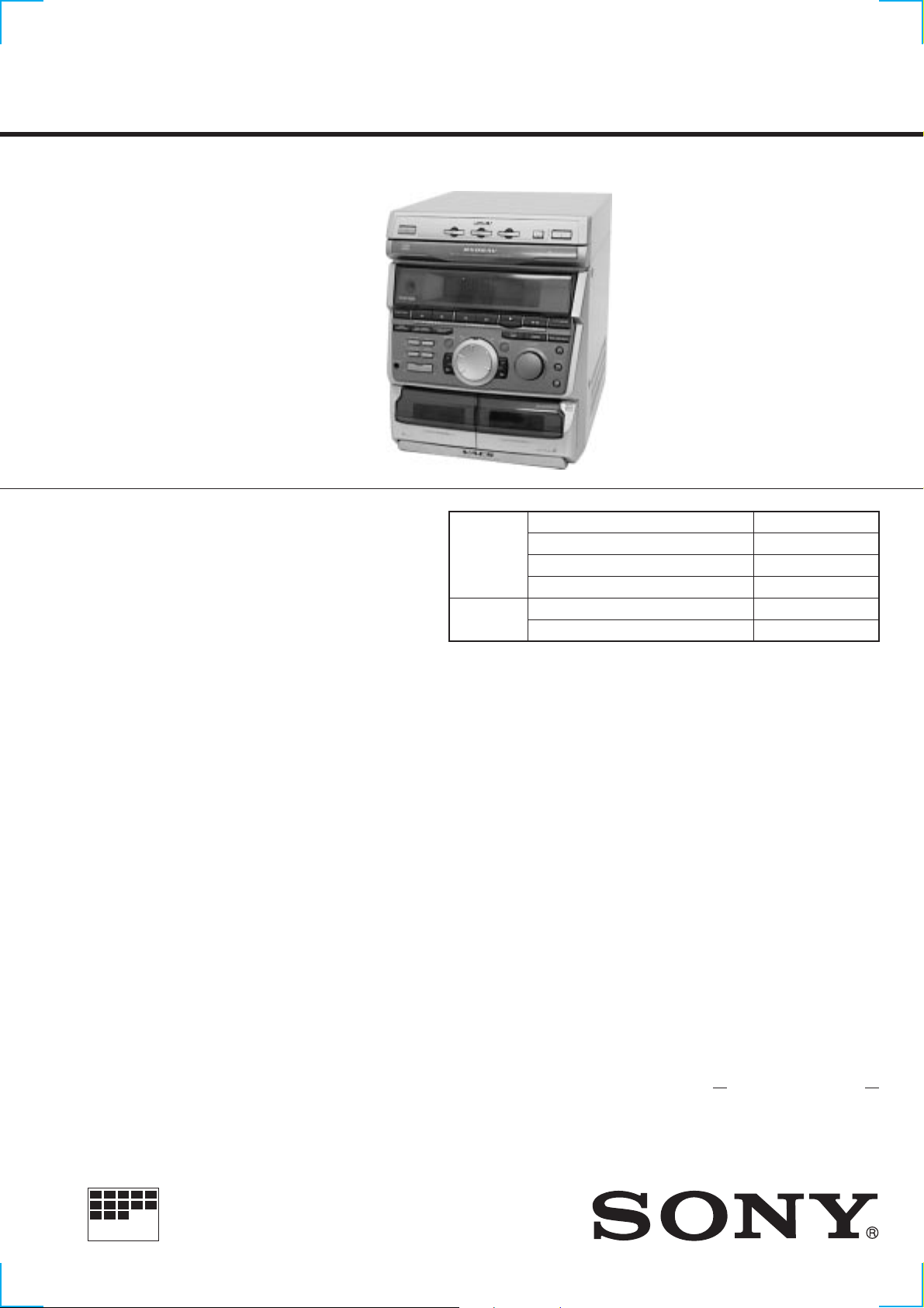
HCD-GRX40AV/RXD6AV
SERVICE MANUAL
HCD-GRX40AV/RXD6A V is the Amplifier ,
CD player, Tape Deck and Tuner section
in MHC-GRX40A V/RXD6AV.
Photo : HCD-RXD6AV
Manufactured under license from Dolby Laboratories
Licensing Corporation.
“DOLBY” and the double-D symbol a are trademarks
of Dolby Laboratories Licensing Corporation.
CD CD Mechanism Type CX3
Section Base Unit Name KSM-213ECM
Tape deck Model Name Using Similar Mechanism HCD-RXD3
Section T ape Transport Mechanism Type CWL-44-RR
AEP Model
UK Model
HCD-RXD6AV
E Model
Australian Model
HCD-GRX40AV
Model Name Using Similar Mechanism HCD-RXD3
Optical Pick-up Name KSS-213ECM/C2NP
Amplifier section
MHC-RXD6AV (Eur opean model):
Front Speaker :
DIN power output (rated)50 + 50 W
(6 Ω at 1 kHz, DIN)
Continuous RMS power output (reference)
60 + 60 W
(6 Ω at 1 kHz, 10% THD)
Music power output (reference)
100 + 100 W
(6 Ω at 1 kHz, 10% THD)
Center Surround Speaker :
DIN power output (rated) 25 W
(12 Ω at 1 kHz, DIN)
Continuous RMS power output (reference)
30 W
(12 Ω at 1 kHz, 10% THD)
Music power output (reference)
50 W
(12 Ω at 1 kHz, 10% THD)
Rear Surround Speaker :
DIN power output (rated) 12.5 + 12.5 W
(6 Ω at 1 kHz, DIN)
Continuous RMS power output (reference)
15 + 15 W
(6 Ω at 1 kHz, 10% THD)
Music power output (reference)
25 + 25 W
(6 Ω at 1 kHz, 10% THD)
SPECIFICA TIONS
MHC-GRX40AV (Other model):
The following measured at AC 120, 240 V, 50/60 Hz
Front Speaker :
DIN power output (rated)60 + 60 W
(6 Ω at 1 kHz, DIN)
Continuous RMS power output (reference)
70 + 70 W
(6 Ω at 1 kHz, 10% THD)
Center Surround Speaker :
DIN power output (rated) 25 W
(12 Ω at 1 kHz, DIN)
Continuous RMS power output (reference)
30 W
(12 Ω at 1 kHz, 10% THD)
Rear Surround Speaker :
DIN power output (rated) 12.5 + 12.5 W
(6 Ω at 1 kHz, DIN)
Continuous RMS power output (reference)
15 + 15 W
(6 Ω at 1 kHz, 10% THD)
Inputs
MD/VIDEO IN : voltage 450 mV/250 mV
(phono jacks) inpedance 47 kΩ
MINI Hi-Fi COMPONENT SYSTEM
Outputs
MD/VIDEO OUT : voltage 250 mV
(phono jacks) impedance 1 kΩ
PHONES : accepts headphones of 8 Ω or
(stereo phone jack) more
FRONT SPEAKER : accepts impedance of 6 to 16 Ω
REAR SPEAKER : accepts impedance of 6 to 16 Ω
CENTER SPEAKER : accepts impedance of 12 to 16 Ω
SUPER WOOFER : Voltage 1 V, impedance 1 kΩ
CD player section
System Compact disc and digital audio
system
Laser Semiconductor laser (λ=780nm)
Emission duration: continuous
Laser output Max. 44.6 µW*
*This output is the value
measured at a distance of 200
mm from the objective lens
surface on the Optical Pick-up
Block with 7 mm aperture.
Frequency response 20 Hz - 20 kHz (±0.5 dB)
Wavelength 780 -790 nm
Signal-to-noise ratio More than 90 dB
Dynamic range More than 90 dB
Continued on next page
MICROFILM

CD DIGITAL OUT
(Square optical connector jack, rear panel)
Wavelength 600 nm
Output Level –18 dBm
Tape player section
Recording system 4-track 2-channel stereo
Frequency response 60 - 13,000 Hz (±3 dB),
(DOLBY NR OFF) using Sony TYPE I cassette
Tuner section
FM stereo, FM/AM superheterodyne tuner
FM tuner section
Tuning range 87.5 - 108.0 MHz
Antenna FM lead antenna
Antenna terminals 75 Ω unbalanced
Intermediate frequency 10.7 MHz
AM tuner section
Tuning range 531 - 1,602 kHz
Antenna AM loop antenna
Antenna terminals External antenna terminal
Intermediate frequency 450 kHz
(with the interval set at 9 kHz)
530 - 1,710 kHz
(with the interval set at 10 kHz)
General
Power requirements
European model: 230 V AC, 50/60 Hz
Australian and South African models:
Mexican model: 120 V AC, 50/60 Hz
Power consumption 190 W
Dimensions (w/h/d) Approx. 280 × 340 × 390 mm
Mass: Approx. 9.2 kg
Design and specifications are subject to change without notice.
240 V AC, 50/60 Hz
(111/8 × 131/2 × 153/8 in.)
(20 lb 5 oz.)
SAFETY-RELATED COMPONENT WARNING!!
COMPONENTS IDENTIFIED BY MARK ! OR DO TTED LINE WITH
MARK ! ON THE SCHEMATIC DIAGRAMS AND IN THE PARTS
LIST ARE CRITICAL TO SAFE OPERATION. REPLACE THESE
COMPONENTS WITH SONY PARTS WHOSE PART NUMBERS
APPEAR AS SHOWN IN THIS MANUAL OR IN SUPPLEMENTS
PUBLISHED BY SONY.
2
TABLE OF CONTENTS
1. SERVICING NOTES ··················································· 3
2. GENERAL ······································································ 4
3. DISASSEMBLY
3-1. CD door ·············································································· 6
3-2. CD Mechanism Deck ························································· 6
3-3. Front Panel ········································································· 7
3-4. Main Board········································································· 7
3-5. Key Board··········································································· 8
3-6. Mech Deck ········································································· 8
3-7. Front Panel (B) ··································································· 9
3-8. Front Board, H/P Board······················································ 9
3-9. Front AMP Board, AMP Board, Photo Socket Board, Fuse
Board ················································································ 10
3-10. CD Tray ············································································ 10
3-11. CD Decord Board ····························································· 11
3-12. Base Unit ·········································································· 12
3-13. Cassette Lid (A)/(B) ························································· 12
4. TEST MODE ································································ 13
5. MECHANICAL ADJUSTMENTS··························14
6. ELECTRICAL ADJUSTMENTS ··························· 14
7. DIAGRAMS
7-1. Block Diagrams
Tuner CD Section ························································ 19
Main Section ·······························································20
7-2. Circrit Boards Location ···················································· 21
7-3. Printed Wiring Board Main Section ······························ 22
7-4. Schematic Diagram Tuner Section ································ 23
7-5. Schematic Diagram Dolby Section ······························· 24
7-6. Schematic Diagram Tape Power Section······················· 25
7-7. Printed Wiring Board Front Section ······························ 26
7-8. Schematic Diagram Front Section································· 27
7-9. Printed Wiring Board FLD Section ······························· 28
7-10. Schematic Diagram FLD Section·································· 29
7-11. Printed Wiring Board CD Section································· 30
7-12. Schematic Diagram CD Section···································· 31
7-13. Printed Wiring Board Center/Rear AMP Section ·········· 32
7-14. Schematic Diagram Center/Rear AMP Section············· 33
7-15. Schematic Diagram Front AMP Section ······················· 34
7-16. Printed Wiring Board Front AMP Section ····················35
7-17. IC Block Diagrams ··························································· 36
7-23. IC PIN Function Description············································40
SECTION 1
SERVICING NOTES
NOTES ON HANDLING THE OPTICAL PICK-UP
BLOCK OR BASE UNIT
The laser diode in the optical pick-up block may suffer electrostatic
break-down because of the potential difference generated by the
charged electrostatic load, etc. on clothing and the human body.
During repair, pay attention to electrostatic break-down and also
use the procedure in the printed matter which is included in the
repair parts.
The flexible board is easily damaged and should be handled with
care.
NOTES ON LASER DIODE EMISSION CHECK
The laser beam on this model is concentrated so as to be focused on
the disc reflective surface by the objective lens in the optical pickup block. Therefore, when checking the laser diode emission,
observe from more than 30 cm away from the objective lens.
Notes on chip component replacement
• Never reuse a disconnected chip component.
• Notice that the minus side of a tantalum capacitor may be damaged by heat.
Flexible Circuit Board Repairing
• Keep the temperature of the soldering iron around 270 ˚C during repairing.
• Do not touch the soldering iron on the same conductor of the
circuit board (within 3 times).
• Be careful not to apply force on the conductor when soldering
or unsoldering.
CAUTION
Use of controls or adjustments or performance of procedures
other than those specified herein may result in hazardous
radiation exposure.
This appliance is classified as a CLASS 1 LASER product.
The CLASS 1 LASER PRODUCT MARKING is located on
the rear exterior.
8. EXPLODED VIEWS
8-1. Cabinet Section································································· 42
8-2. Front Panel Section-1 ······················································· 43
8-3. Front Panel Section-2 ······················································· 44
8-4. CD Mechanism Deck Section-1 ······································· 45
8-5. CD Mechanism Deck Section-2 ······································· 46
8-6. Base Unit Section (KSM-213ECM)································· 47
9. ELECTRICAL PARTS LIST ··································· 48
Laser component in this product is capable of emitting radiation
exceeding the limit for Class 1.
The following caution label is located inside the unit.
3
@£
@™
@¡
@º
!ª
!•
!¶
!§
!∞
SECTION 2
GENARAL
12 34
5
6
7
8
9
0
!¡
!™
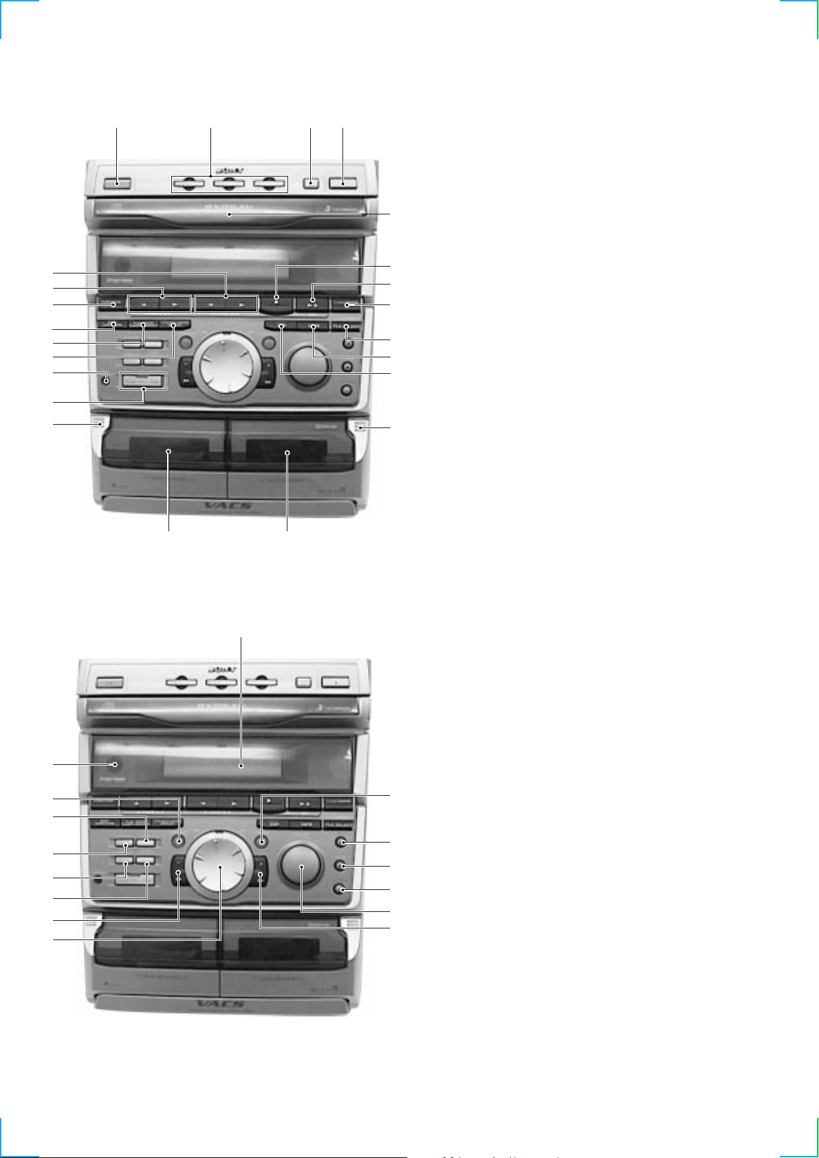
1 1/u (Power) button and indicator
2 DISC 1 to 3 button and indicators
3 DISC SKIP button
4 § (CD) button
5 CD disc tray
6 p button
7 CD, ^ button and indicator
8 TUNER/BAND button
9 FILE SELECT button
0 DBFB button
!¡ DSP button
!™ § (deck B)
!£ Tape deck B
!¢ Tape deck A
!∞ § (deck A)
!§ DOLBY PRO LOGIC button
!¶ PHONES jack
!• REPEAT, STEREO/MONO button
!ª PLAY MODE, TUNER MEMORY button
@º EDIT DIRECTION button
@¡ FUNCTION button
@™ TAPE A, 9 and ( buttons and indications
@£ TAPE B, 9 and ( buttons and indications
#•
#¶
#§
#∞
#¢
#£
#™
#¡
@¢
!£!¢
@¢ Fluorescent indicator tube
@∞ ENTER/NEXT button and indicator
@§ REC button and indicator
@¶ PAUSE button
@• CD SYNC button
@ª VOLUME knob
#º +, ) button and indicator
#¡ JOG dial
@∞
#™ –, 0 button and indicator
#£ TIMER SELECT button and indicator
#¢ CLOCK/TIMER SET button
@§
@¶
#∞ DISPLAY button
#§ DEMO button
#¶ GROOVE button and indicator
#• Remote sensor
@•
@ª
#º
4
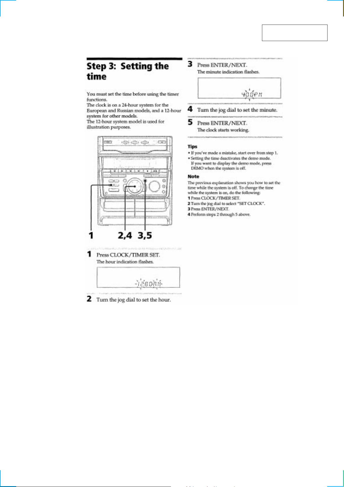
This section is extracted
from instruction manual.
5
)
SECTION 3
DISASSEMBLY
Note : Follow the disassembly procedure in the numerical order given.
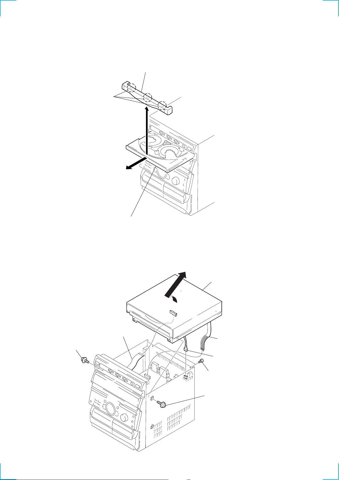
3-1. CD DOOR
2
CD door
Three claws
1
Pull out the CD tray and remove the CD door
with releasing claws into the direction of arrow.
3-2. CD MECHANISM DECK
2
Screw (PTPWH 3 × 10)
4
Flat type wire (CN705)
7
CD mechanism deck
5
Harness (CN304
6
Connector (CN703)
3
Screws (BVTP 3 × 10)
1
Screw (PTPWH 3 × 10)
6
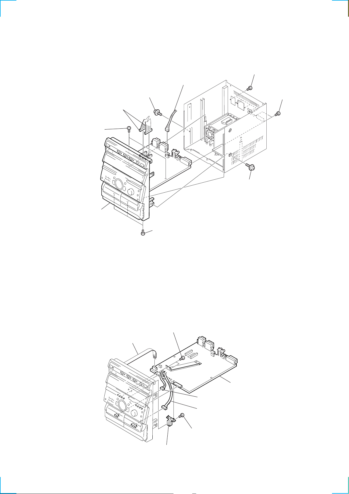
3-3. FRONT PANEL
)
d
1
(CN302)
6
Screws
(BVTP 3
9
Front panel
Connector (CN301)
×
10)
5
Screw
(PTPWH 3
2
Connector (CN502)
×
10)
8
Screws (BVTP 3 × 10)
7
Screws (BVTP 3 × 14
4
Screw (PTPWH 3 × 10)
3-4. MAIN BOARD
1
Harness (CN303)
3
Screws (BVTT 3 × 10)
6
Screws (BVTP 3 × 10)
7
2
Connector (CN201)
MAIN boar
5
PWB stopper
3
Connector (CN202)
4
Screw (BVTP 3 × 8)
7
)
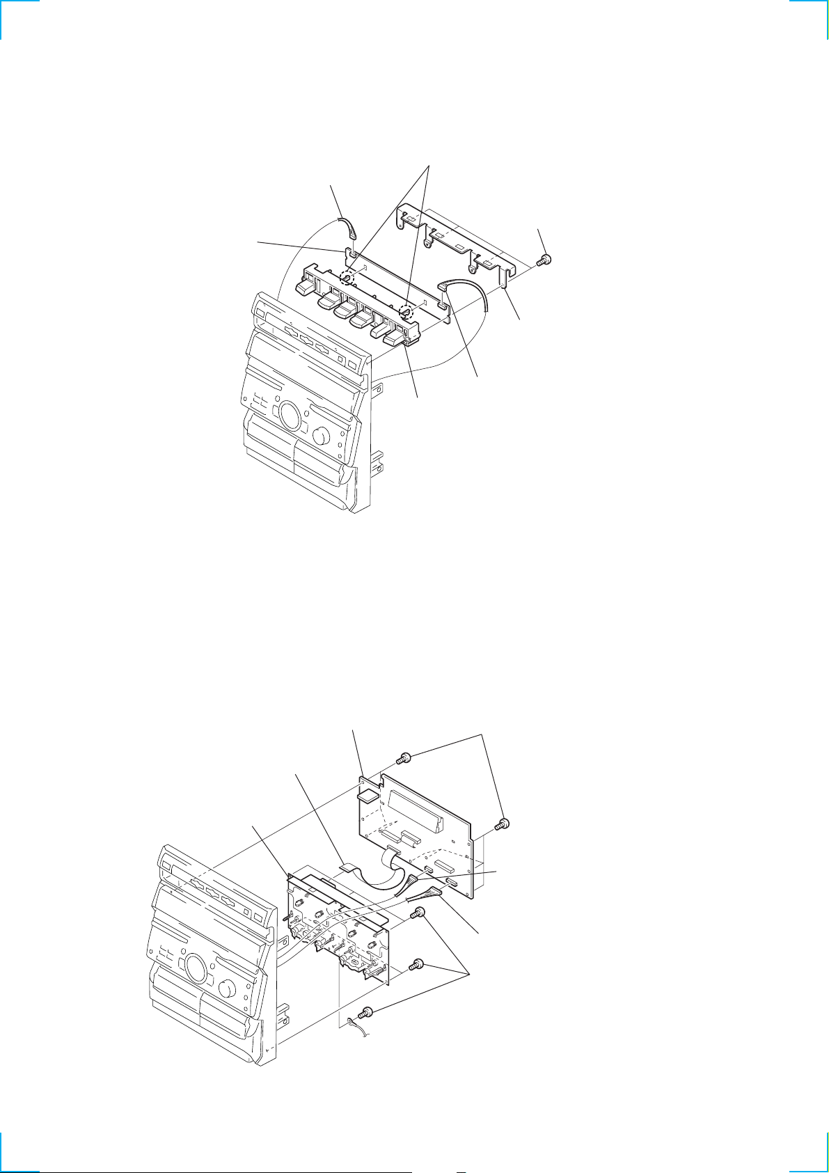
3-5. KEY BOARD
)
6
KEY BOARD
3
Connector (CN607)
Two claws
5
Button
1
Screws (BVTP 3 × 12
2
CD PC board
bracket
4
Connector (CN606)
3-6. MECH DECK, FLD BOARD
1
Flat type wire (CN603)
3
Mech deck
7
FLD board
4
Screws (BVTP 3 × 10)
5
6
Connector (CN602)
2
Screws (BVTP 3 × 8)
Connector (CN601
8
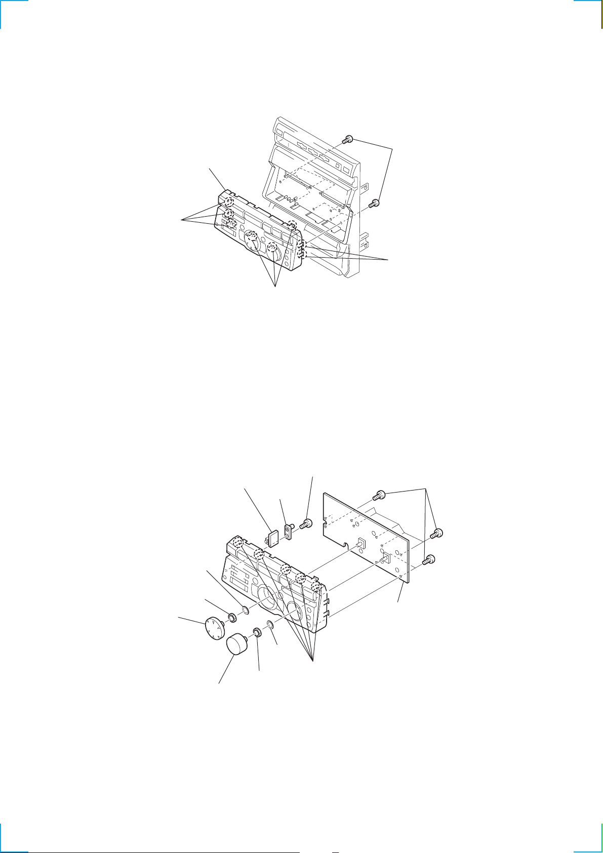
3-7. FRONT PANEL (B)
)
Three claws
2
Front panel (B)
Three claws
1
Screws (BVTP 3 × 10
Two claws
3-8. FRONT BOARD, H/P BOARD
9
Washer
(VR601)
3
Nut
(VR601)
1
Jog knob
2
Volume knob
H/P board
4
Nut(VR602)
7
Screw (BVTP 3 × 10)
8
Holder
Washer
(VR602)
Five claws
5
Screws (BVTP 3 × 10)
6
Front board
9
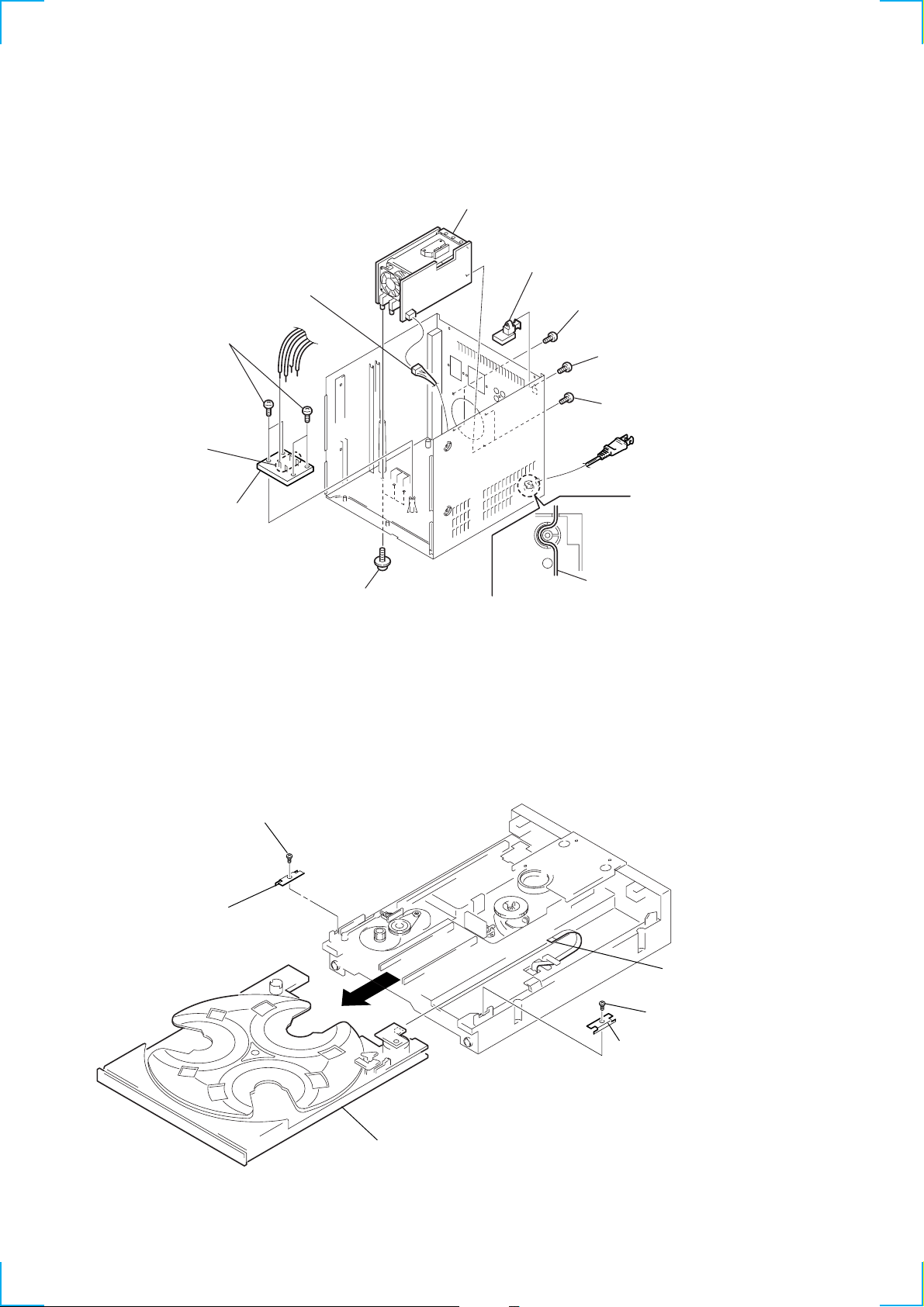
3-9. FRONT AMP BOARD, AMP BOARD, PHOTO SOCKET BOARD, FUSE BOARD
)
5
Front amp/Amp board
7
Photo socket board
1
9
Screws (BVTP 3 × 10)
8
Remove the four
solderings
0
Fuse board
Connector (CN501)
3
Screws (BVTP 3 × 10)
6
Screw (BVTP 3 × 10)
2
HOW TO SET THE
POWER CORD
Screws (BVTP 3 × 10
3-10. CD TRAY
2
Bracket
4
1
Screw (+P 2.6 × 4)
Screws (P 4 × 12)
Power cord
5
Flat type wire
(CN06)
3
Screw (+P 2.6 × 4)
10
6
CD tray
4
Bracket
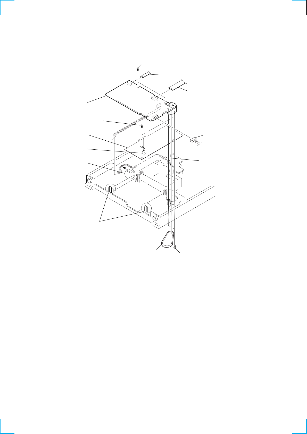
3-11. CD DECORD BOARD
0
CD decord board
7
T wo screw
(+BVTP 3
8
Sheet
Claw
Claw
×
10)
1
Two screws (+BVTP 3 × 10)
6
Flat type wire (CN06)
5
Flat type wire (CN01)
4
Connector (CN05)
9
Connector (CN03)
Two claws
3
Belt
2
Two screws (+BVTP 3 × 10)
11
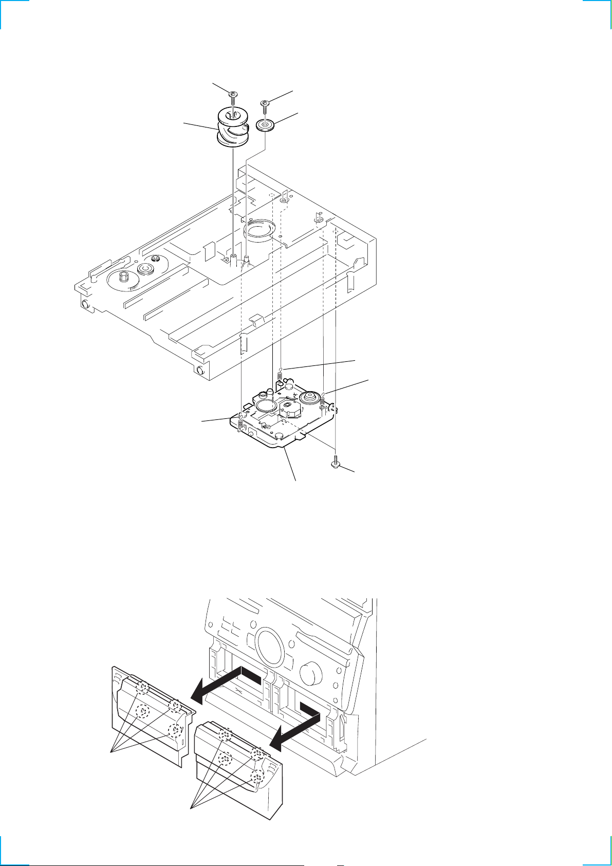
3-12. BASE UNIT
5
UD-cam
4
Screw (+PTPWH 2.6 × 8)
2
Screw (+PTPWH 3 × 8)
3
UD-gear
7
Spring
3-13. CASSETTE LID (A)/(B)
8
Spring
1
9
Base unit
1
Remove the cassette lids in the direction of arrow.
6
Spring
Two screws (+KTP 3 × 8)
12
Four claws
Four claws

SECTION 4
TEST MODE
Initialization
Press the STOP button and POWER OFF button at the same time.
All preset data is re-set to the initial (default) value.
Model display
Press the STOP button and DISC 1 button at the same time.
Model name is displayed.
Destination display
Press the STOP button and DISC 2 button at the same time.
Destination is displayed.
Version display
Press the STOP button and DISC 3 button at the same time.
Version number of the microprocessor is displayed.
CD aging mode
Press the STOP button and DISC SKIP/EX-CHANGE button at the
same time.
Set discs to DISC 1 and DISC 3. The following operations are
repeated when aging
starts:
1. DISC 1: TOC Read
2. Plays back the last music of the DISC 1
3. DISC 3 : TOC Read
4. Plays back the last music of the DISC 3.
5. STOP
6. Tray is open and closed.
CD service mode
Press the STOP button and OPEN/CLOSE button at the same time.
The message “CD S - -” is displayed on the screen. The sled is
moved to the outer circumference while the FF button is pressed.
Also, the SLED is moved to the inner circumference while the REW
button is pressed. After pressing the PLAY button, FOCUS is turned
ON, CLV-S is set, TRACKING and SLED servos are turned OFF
and ADDRESS 3 = 3F, 37 is set.
Display
Press the STOP button and DBFB button at the same time.
All displays are turned ON.
Balance adjustment value
Press the STOP button and DISPLAY button at the same time.
The balance adjustment value is displayed.
Key check
Press the STOP button and FILE SELECT button at the same time.
Function of the pressed key is displayed.
TAPE aging mode
Press the STOP button and PLAY A button at the same time.
Insert a commercially available cassette tape (10 min) to the decks
A and B. When aging starts, each tape is rewound and the follo wing
operations are repeated:
1. TAPE A: FWD PLAY for one minute
2. TAPE A: FWD STOP for one second
3. TAPE A: FWD PLAY for three minutes
4. TAPE A: FWD FF to tape end
5. TAPE B: FWD PLAY for one minute
6. TAPE B: FWD REC PAUSE for one second
7. TAPE B: FWD REC for three minutes
8. TAPE B: FWD FF to tape end
9. TAPE B: REV PLAY for one minute
10. TAPE B: REV REC PAUSE for one second
11. TAPE B: REV REC for three minutes
12. TAPE B: REV FF to tape end.
13
SECTION 5
MECHANICAL ADJUSTMENTS
SECTION 6
ELECTRICAL ADJUSTMENTS
Precaution
1. Clean the following parts with a denatured alcohol-moistened
swab:
record/playback head pinch rollers
erase head rubber belts
capstan idlers
2. Demagnetize the record/playback head with a head
demagnetizer.
3. Do not use a magnetized screwdriver for the adjustments.
4. After the adjustments, apply suitable locking compound to the
parts adjusted.
5. The adjustments should be performed with the rated power
supply voltage unless otherwise noted.
Torque Measurement
Torque
FWD
FWD
back tension
FF/REW
Torque meter
CQ-102C
CQ-102C
CQ-201B
Meter reading
40 to 70 g • cm
(0.56 - 0.97 oz • inch)
1 to 5 g • cm
(0.01 - 0.07 oz • inch)
55 to 140 g • cm
(0.76 - 1.94 oz • inch)
DECK SECTION 0 dB=0.775V
1. Demagnetize the record/playback head with a head
demagnetizer.
2. Do not use a magnetized screwdriver for the adjustments.
3. After the adjustments, apply suitable locking compound to the
parts adjusted.
4. The adjustments should be performed with the rated power
supply voltage unless otherwise noted.
5. The adjustments should be performed in the order giv en in this
service manual. (As a general rule, playback circuit adjustment
should be completed before performing recording circuit
adjustment.)
6. The adjustments should be performed for both L-CH and RCH.
Tape
P-4-A100
WS-48B
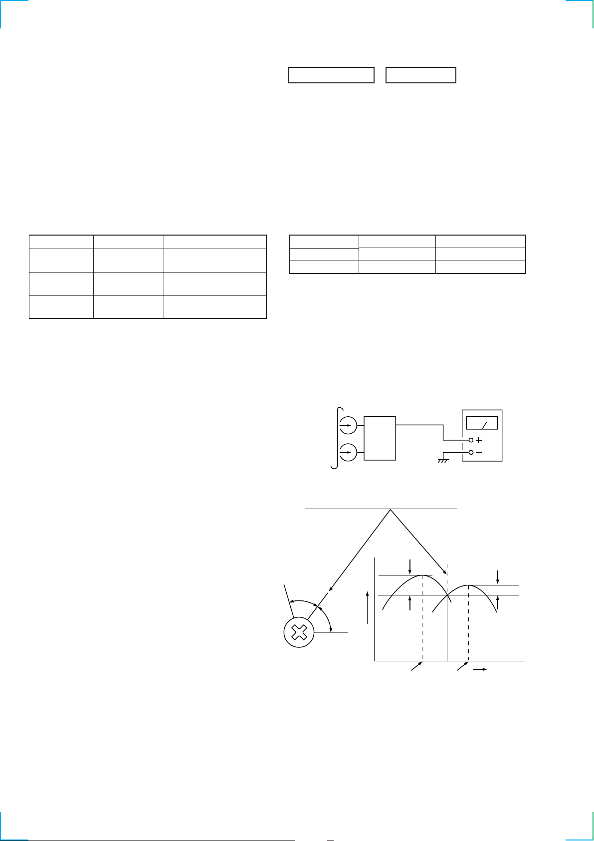
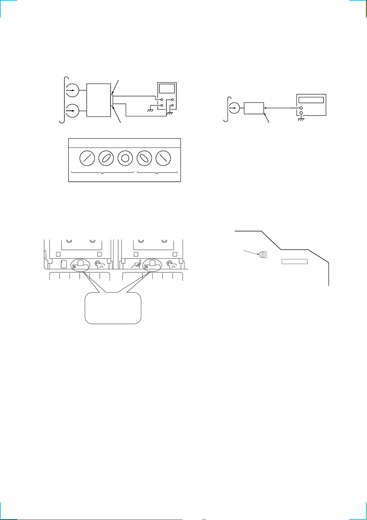
Record/Playback Head Azimuth Adjustment
(Deck A, Deck B)
Note: Perform this adjustments for both decks.
Procedure:
1. Mode : Playback
Signal
10 kHz, –10 dB
3 kHz, 0 dB
Used for
Azimuth Adjustment
Tape Speed Adjustment
test tape
P-4-A100
(10kHz, –10dB)
2. Turn the adjustment scr ew and check output peaks. If the peaks
do not match for L-CH and R-CH, turn the adjustment screw
so that outputs match within 2 dB of peak.
L-CH
peak
screw
position
output
level
R-CH
peak
SPEAKER
terminal (JK401)
set
within
2dB
L-CH
peak
R-CH
peak
level meter
within 2dB
screw
position
14
3. Mode: Playback
e
r
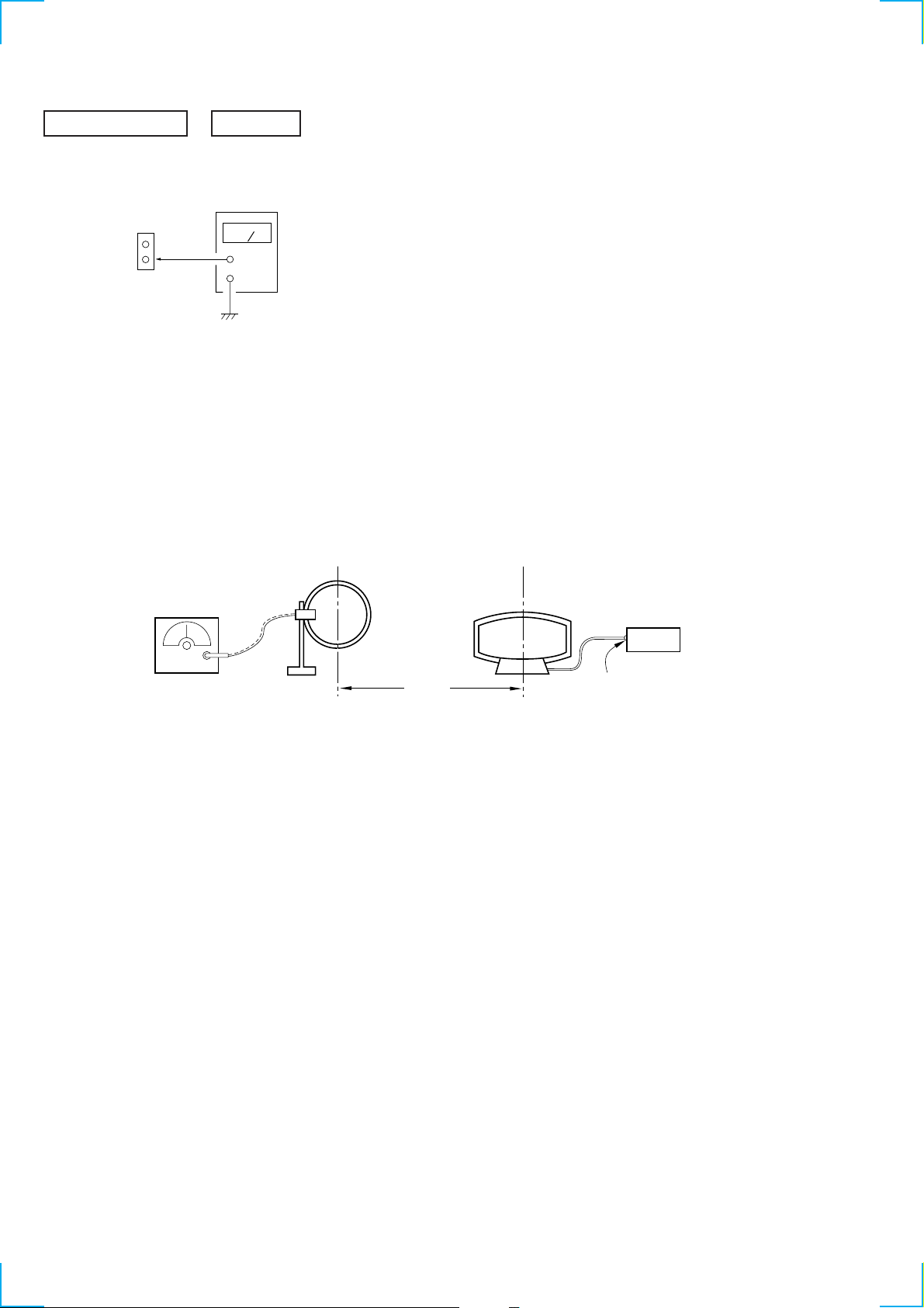
Tape Speed Adjustment (Deck A)
test tape
P-4-A100
(10kHz, –10dB)
in phase 45˚ 90˚ 135˚ 180˚
SPEAKER
terminal (JK401)
(L-CH)
L
R
SPEAKER
terminal (JK401)
(R-CH)
Waveform of oscilloscope
good wrong
oscilloscop
4. After the adjustments, apply suitable locking compound to the
parts adjusted.
Adjustment Location:
Remove the cassette lid before adjustment (See page 9)
Procedure:
1. Mode: Playback
test tape
WS-48B
(3kHz, 0dB)
set
SPEAKER
terminal (JK401)
frequency counte
+
–
2. Adjust the SFR601 so that the frequency counter reads 3,000
Hz ± 90Hz.
Adjustment Location: MAIN board
Sample Value of Wow and flutter
W. RMS (JIS) within 0.3%
(test tape: WS-48B)
[FLD BOARD] — Component side —
Adjustment screws
REC/PB head (deck B)
or PB head (deck A)
Tape Speed
SFR601
CN604
15
TUNER SECTION 0 dB=1µV
r
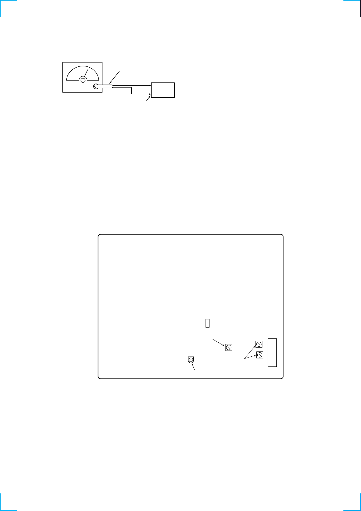
AM T uning Volta ge Adjustment
Main board
TP1
G
VT
DC voltmete
+
–
Procedure:
1. Set the reception frequency of the unit to 530 kHz.
2. Adjust L107 for 1.2 ± 0.05 V reading on the DC voltmeter.
3. Set the reception frequency of the unit to 1,710 kHz.
4. Confirm that the voltage reading on the DC v oltmeter is within
8.0 ± 0.5 V.
Adjustment Location: MAIN board (See page 17)
AM T racking Adjustment
loop antenna
AM RF SSG
loop antenna
(Supplied accessories)
set
30% amplitude
modulation by
400 Hz signal
Field strength dB (
Procedure:
1. Tune the set to 600 kHz.
2. Set the output of AM RF SSG so that the input level of the set
will become 60 dB (µV/m).
3. Adjust L104 so that when the wav eform on the oscilloscope is
maximum, no noise appears.
4. Tune the set to 1,400 kHz.
60 cm
µ
V/m) =SSG output level dB (µV/m) –26 dB.
AM ANTENNA
terminal (TM1)
5. Adjust TC101 so that when the wa v eform on the oscilloscope
is maximum, no noise appears.
• Repeat the procedures in each adjustment several times, and the
tracking adjustment should be finally done by the trimmer
capacitors.
Adjustment Location: MAIN board (See page 17)
16
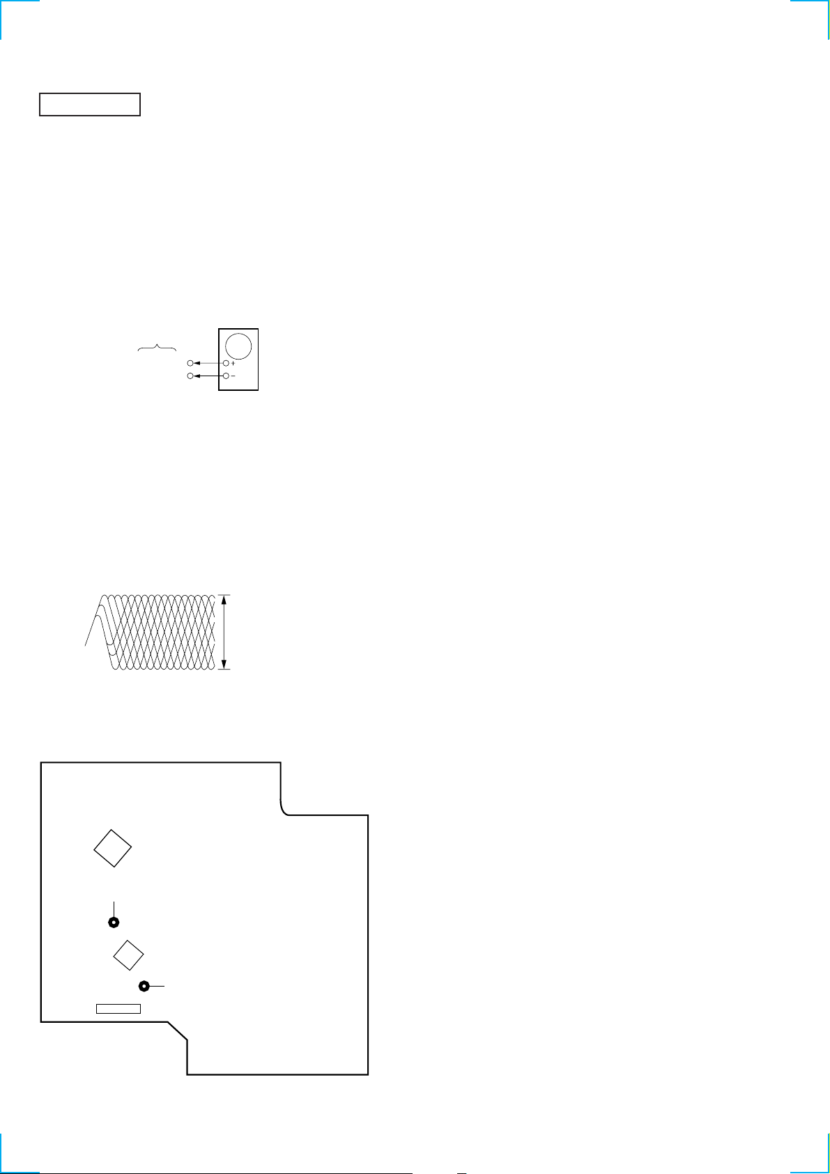
FM Tuned Level Adjustment
FM RF SSG
Ω
coaxial
75
set
Carrier frequency : 98 MHz
Modulation : AUDIO 1 kHz, 75 kHz
deviation (100%)
Output level : 28 dB (at 75 W open)
FM ANTENNA terminal
(JK101)
Procedure:
1. Supply a 28 dB 98 MHz signal from the ANTENN A terminal.
2. Tune the set to 98 MHz.
3. Adjust SFR101 to the point (moment) when the TUNED
indicator will change from going off to going on.
Adjustment Location: MAIN board
Adjustment Location
[MAIN BOARD] Component side
TP1
AM T uning
Voltage
SFR101
FM T uned Level
L107
AM T rac king
L104
TC101
JK101
17
CD SECTION
V
Note:
1. CD Block is basically constructed to operate without
adjustment. Therefore, check each item in order given.
2. Use YEDS-18 disc (3-702-101-01) unless otherwise indicated.
3. Use an oscilloscope with more than 10MΩ impedance.
4. Clean the object lens by an applicator with neutral detergent
when the signal level is low than specified value with the
following checks.
5. Adjust the focus bias adjustment when optical block is replaced.
RF Level Check
CD DECODER
board
TP (RF)
TP (VC)
oscilloscope
Procedure :
1. Connect oscilloscope to test point TP (RF) on CD DECODER
board.
2. Turned Power switch on.
3. Put disc (YEDS-18) in and playback.
4. Confirm that oscilloscope waveform is clear and check RF
signal level is correct or not.
Note: Clear RF signal waveform means that the shape “◊” can be
clearly distinguished at the center of the waveform.
VOLT/DIV: 200 m
TIME/DIV: 500 nS
level: 1.0 Vp-p
+0.3
–0.2
Adjustment Location:
[CD DECODER BOARD] Component side
IC702
J778
TP (VC)
IC701
J789
CN701
TP
(RF)
18
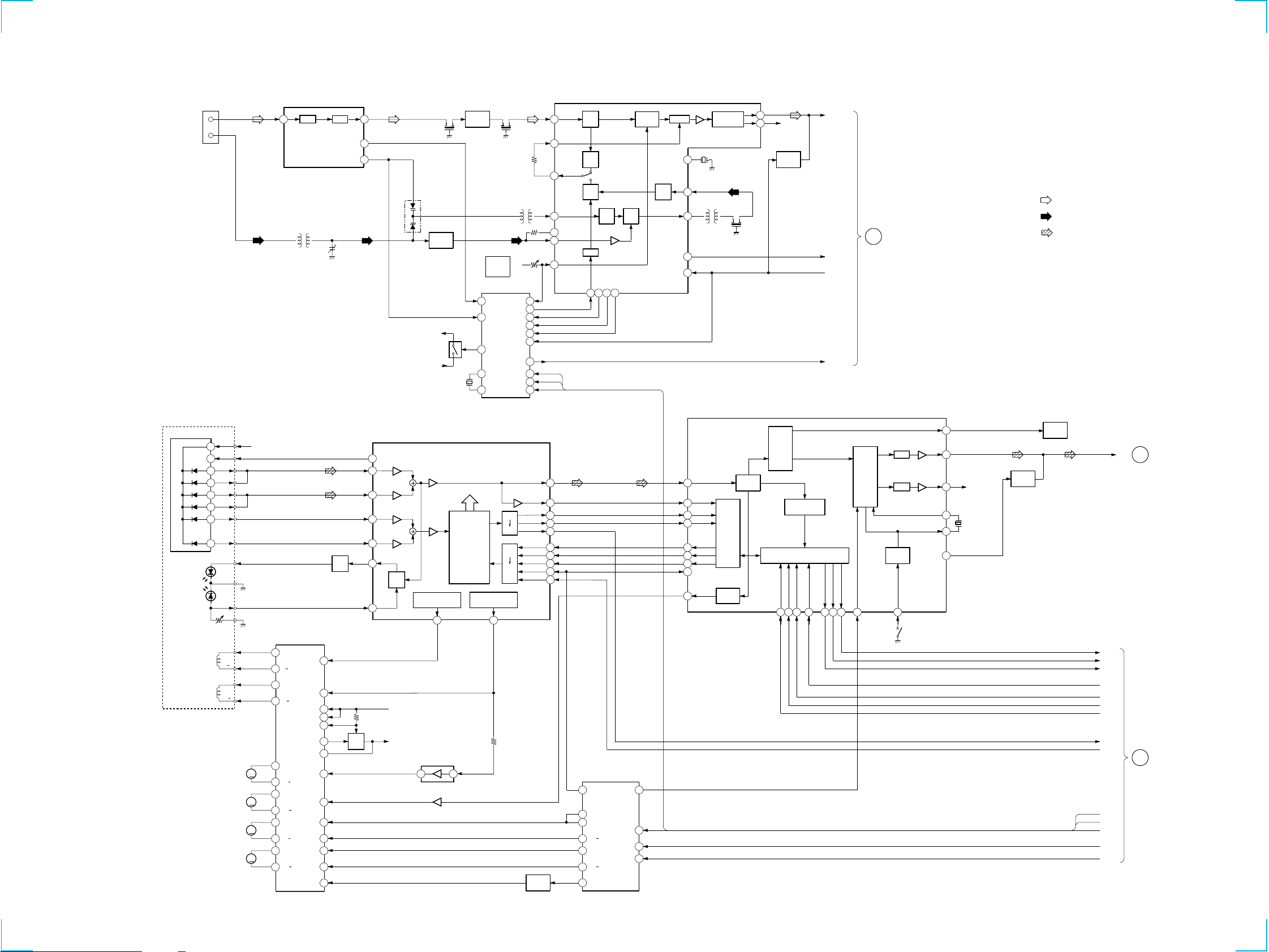
7-1. BLOCK DIAGRAMS
TUNER/CD SECTION
FM
AM
JK101
SECTION 7
HCD-GRX40AV/RXD6AV
DIAGRAMS
FM
IF
FM
DET
AM
DET
AGC
SMET
20
FM/AM MPX
AM
OSCAMMIX
TU LED
ST MONO
12
6
11
IC102
PH DET
AM/FM
IF BUFF
AM
IF
FM DET
ST IND
AM/FM
MUTE
L
CF103
450kHz
13
R
14
R CH
Q109
MUTE
DECODER
CF104
8
10.7MHz
4
T102
AM IFT
2
7
10
TU L
ST IND
TU MUTE
DO
A
MAIN
SECTION
(Page 20)
• RCH is omitted
• SIGNAL PATH
:FM
:AM
:CD
FM FRONT END
FE101
8
RF
L104
AM ANT
MIX
TC101
1
3
OSC
4
VT
D105
Q104
AM RF
AMP
TUB+
Q103
+12V
CF101
10.7MHz
X201
7.2MHz
Q101
RF IF
AMP
CF102
10.7MHz
L107
MW OSC
SFR101
FM
B+
TUNED
LEVEL
PLL
IC103
FM
PD1
FM B+
XO
XI
SD SPEED
SD IN
ST/MONO
AM/FM
IF IN
CLK
AM
DO
DI
CE
16
18
7
22
1
FM IF
1
MPX
16
FM OUT
19
OSC
23
AFC
22
AM RF
21
OSC/FMSD
24
15
10
11
9
8
12
DO
6
DI
4
CLK
5
CE
3
16
OPTICAL PICK-UP
BLOCK
DETECTOR
7
8
4
1
2
5
6
10
LD
PD
FOCUS
COIL
TRACKING
COIL
GND
VR
VC
A
C
B
D
E
F
LD
PD
F+
F
T+
T
M102
SLED
MOTOR
M101
SPINDOL
MOTOR
T/T
MOTOR
TRAY
MOTOR
MUTE
PH701
DIGITAL
OUT
SCOR
SENS1
SQSO
XLAT
SQCK
CLK
DATA
SENS2
LOCK
DI
CLK
CE
DATA IN
STB
CD L
B
MAIN
SECTION
(Page 20)
C
MAIN
SECTION
(Page 20)
GEN.
PWM
PWM
15
SPOA
D OUT
L MUTE
XTA1
XTA0
53
NL
67
Q705,707
NR
74
R-CH
70
X701
16.9344MHz
71
2
CD RF/SERVO
PROSSESOR
+5V
VC
51
PD1
38
PD2
39
E
42
F
Q703
41
LD
36
APC
PD
PD
37
B+
REG
+5V
Q701
APC
F/T COIL
SL/SP MOTOR
T.T/TRAY MOTOR
DRIVER
IC703
2
F+
F IN
REG I
REG B
REG OUT
SL IN
SP IN
T.T F IN
T.T R IN
TR F IN
TR T IN
MUTE IN
6
T IN
5
VCC
8
VCC
7
9
10
11
22
21
13
12
29
28
27
1
F
3
T+
4
T
SL+
18
M
SL
17
SP+
19
M
SP
20
T.T+
14
M
T.T
15
TR+
30
M
TR
31
IC701 (1/2)
RF
AMP
FE
AMP
FOCUS PHASE
COMPENSATION
FEO TAO
6
IC701 (2/2)
16
IC705
67
COMAND
PARALLEL
CONVERTER
DECODER
14
SERIAL/
TRACKING PHASE
COMPENSATION
13
RFO
33
FOK
27
C OUT
IIL
TTL
TTL
IIL
SENS1
SENS2
DATA
XLT
CLK
XRST
LOCK
Q702
SWITCH
24
25
26
22
21
20
23
19
T.T/TRAY
MOTOR DRIVE
REG CONTROL
IC704
XRST
CONTROL
T.T+
T.T
TR+
TR
CONTROL
MUTE
CLOK
DATA
4
3
2
STB
1
6
11
7
14
13
12
5
RF
35
FOK
18
CIN
11
SE
10
DAT
12
XLT
13
CLK
14
79
XRST
MDP
21
CD DIGITAL
SIGNAL PROCESSOR
IC702
DEMO.
CLV
SERVO
DIGITAL
CLV
D/A
I/F
SERIAL
I/F
EFM
SUB CODE
PROSSESOR
S05
STOP
SWITCH
CLOCK
CPU I/F
SQSO
SENS
XLAT
SQCK
CLOK
DATA
7 9 4 5 6 6257
8
SCOR
SYS M
19
19
 Loading...