

Page 1
HCD-GNZ333D/GNZ444D
SERVICE MANUAL
Ver. 1.4 2008.09
• HCD-GNZ333D/GNZ444D are the tuner,
deck, DVD and amplifier section in
MHC-GNZ333D/GNZ333DL/GNZ444D.
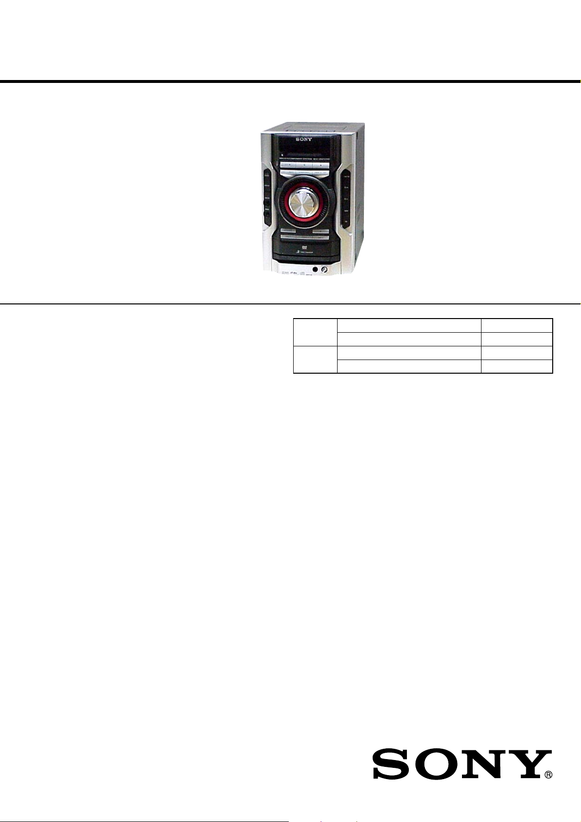
(Photo: HCD-GNZ444D)
DVD
Section
Tape Deck
Section
SPECIFICATIONS
E Model
Model Name Using Similar Mechanism NEW
Optical Pick-up Name KHM-313CAB
Model Name Using Similar Mechanism HCD-EC55/EC77
Tape Transport Mechanism Type CS-21SC-901TP
Amplifier section
The following are measured at AC 120, 127,
220, 240V 50/60 Hz
Front speaker:
Power output (rated)
72 W + 72 W (at 6 Ω, 1 kHz, 1%
THD)
RMS output power (reference)
120 W + 120 W (per channel at 6 Ω,
1 kHz, 10% THD)
Subwoofer (HCD-GNZ444D only):
RMS output power (reference)
150 W (at 6 Ω, 80 Hz, 10% THD)
Inputs
AUDIO IN (stereo mini jack):
Voltage 700 mV, impedance
47 kilohms
Outputs
DIGITAL OUT (square optical connector
jack):
Wavelength 650 nm
VIDEO OUT (phono jack):
Max. output level 1 Vp-p, unbalanced,
Sync. negative load impedance 75 Ω
PHONES (stereo mini jack):
accepts headphones of 8 Ω or more
SUBWOOFER OUT (HCD-GNZ444D
only)
Power consumption:
190 W
Dimensions (w/h/d):
Approx. 200 × 306 × 410 mm
Mass:
Approx. 8.0 kg
Disc player section
System
Compact disc and digital audio and
video system
Laser
Semiconductor laser (DVD:
λ=650 nm, CD: λ=790 nm)
Emission duration: continuous
Frequency response
DVD (PCM 48 kHz): 2 Hz – 22 kHz
(±1dB)
CD: 2 Hz – 20 kHz (±0.5 dB)
Video color system format
NTSC and PAL
Tape deck section
Recording system: 4-track 2-channel, stereo
– Continued on next page –
9-887-709-05
2008I04-1
© 2008.09
DVD DECK RECEIVER
Sony Corporation
Audio&Video Business Group
Published by Sony Techno Create Corporation
Page 2

HCD-GNZ333D/GNZ444D
Tuner section
FM stereo, FM/AM superheterodyne tuner
FM tuner section
Tuning range:
87.5 – 108.0 MHz (50 kHz step)
Antenna
FM lead antenna
Antenna terminals
75 Ω unbalanced
Intermediate frequency
10.7 MHz
AM tuner section
Tuning range:
Saudi Arabian and Russian models:
531 – 1,602 kHz (with the interval set
at 9 kHz)
Other models:
531 – 1,602 kHz (with the interval set
at 9 kHz)
530 – 1,610 kHz (with the interval set
at 10 kHz)
Antenna
AM loop antenna
Antenna terminals
External antenna terminal
Intermediate frequency
450 kHz
General
Power requirements:
Russian model:
AC 220 – 240 V, 50/60 Hz
Saudi Arabian model:
AC 120 – 127, 220 – 240 V,
50/60 Hz, adjustable with voltage
selector
Other models:
AC 120, 220 or 230 – 240 V,
50/60 Hz, adjustable with voltage
selector
Design and specifications are subject to
change without notice.
U.S. and foreign patents licensed from
Dolby Laboratories.
SAFETY-RELATED COMPONENT WARNING!!
COMPONENTS IDENTIFIED BY MARK 0 OR DOTTED LINE
WITH MARK 0 ON THE SCHEMATIC DIAGRAMS AND IN
THE PARTS LIST ARE CRITICAL TO SAFE OPERATION.
REPLACE THESE COMPONENTS WITH SONY P AR TS WHOSE
PART NUMBERS APPEAR AS SHOWN IN THIS MANU AL OR
IN SUPPLEMENTS PUBLISHED BY SONY.
2
Page 3
HCD-GNZ333D/GNZ444D
Ver. 1.2
Notes on chip component replacement
• Never reuse a disconnected chip component.
• Notice that the minus side of a tantalum capacitor may be
damaged by heat.
Flexible Circuit Board Repairing
• Keep the temperature of the soldering iron around 270 ˚C
during repairing.
• Do not touch the soldering iron on the same conductor of the
circuit board (within 3 times).
• Be careful not to apply force on the conductor when soldering
or unsoldering.
UNLEADED SOLDER
Boards requiring use of unleaded solder are printed with the leadfree mark (LF) indicating the solder contains no lead.
(Caution: Some printed circuit boards may not come printed with
the lead free mark due to their particular size)
: LEAD FREE MARK
Unleaded solder has the following characteristics.
• Unleaded solder melts at a temperature about 40 ˚C higher
than ordinary solder.
Ordinary soldering irons can be used but the iron tip has to be
applied to the solder joint for a slightly longer time.
Soldering irons using a temperature regulator should be set to
about 350 ˚C.
Caution: The printed pattern (copper foil) may peel away if
the heated tip is applied for too long, so be careful!
• Strong viscosity
Unleaded solder is more viscou-s (sticky, less prone to flow)
than ordinary solder so use caution not to let solder bridges
occur such as on IC pins, etc.
• Usable with ordinary solder
It is best to use only unleaded solder but unleaded solder may
also be added to ordinary solder.
NOTES ON LASER DIODE EMISSION CHECK
The laser beam on this model is concentrated so as to be focused on
the disc reflective surface by the objective lens in the optical pickup block. Therefore, when checking the laser diode emission,
observe from more than 30 cm away from the objective lens.
Laser component in this product is capable
of emitting radiation exceeding the limit for
Class 1.
This appliance is
claassified as a CLASS 1
LASER product. This
label is located on the
rear exterior.
CAUTION
Use of controls or adjustments or performance of procedures
other than those specified herein may result in hazardous radiation
exposure.
NOTES ON HANDLING THE OPTICAL PICK-UP
BLOCK OR BASE UNIT
The laser diode in the optical pick-up block may suffer electrostatic
break-down because of the potential difference generated by the
charged electrostatic load, etc. on clothing and the human body.
During repair, pay attention to electrostatic break-down and also
use the procedure in the printed matter which is included in the
repair parts.
The flexible board is easily damaged and should be handled with
care.
3
Page 4
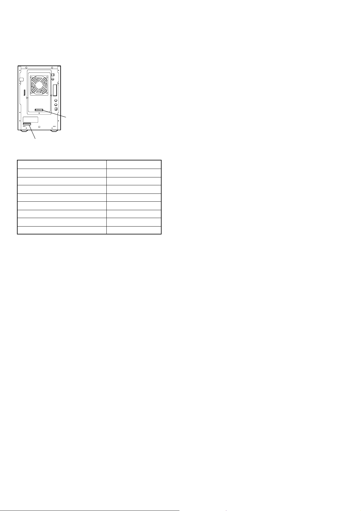
HCD-GNZ333D/GNZ444D
)
MODEL IDENTIFICATION
– BACK PANEL –
PARTS No. (TH model
PARTS No. (except TH model)
Model Part No.
GNZ333D: SP 2-898-299-0s
GNZ444D: E13 2-898-299-1s
GNZ333D: EA 2-898-299-2s
GNZ333D: E13 2-898-299-3s
GNZ333D: E3, E15 2-898-299-4s
GNZ333D: PH 2-898-299-5s
GNZ333D: TH 2-898-299-6s
GNZ333D: E12 2-898-299-7s
•Abbreviation
E3 : 240 V AC area in E model
E12 : 220-240 V AC area in E model
E13 : Russian model
E15 : Iran model
EA : Saudi Arabia model
PH : Philippine model
SP : Singapore model
TH : Thai model
4
Page 5

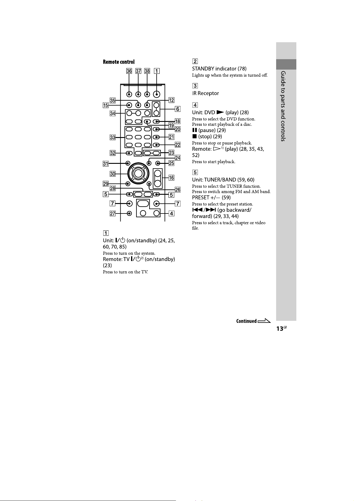
TABLE OF CONTENTS
HCD-GNZ333D/GNZ444D
1. SERVICING NOTES ............................................... 6
2. GENERAL
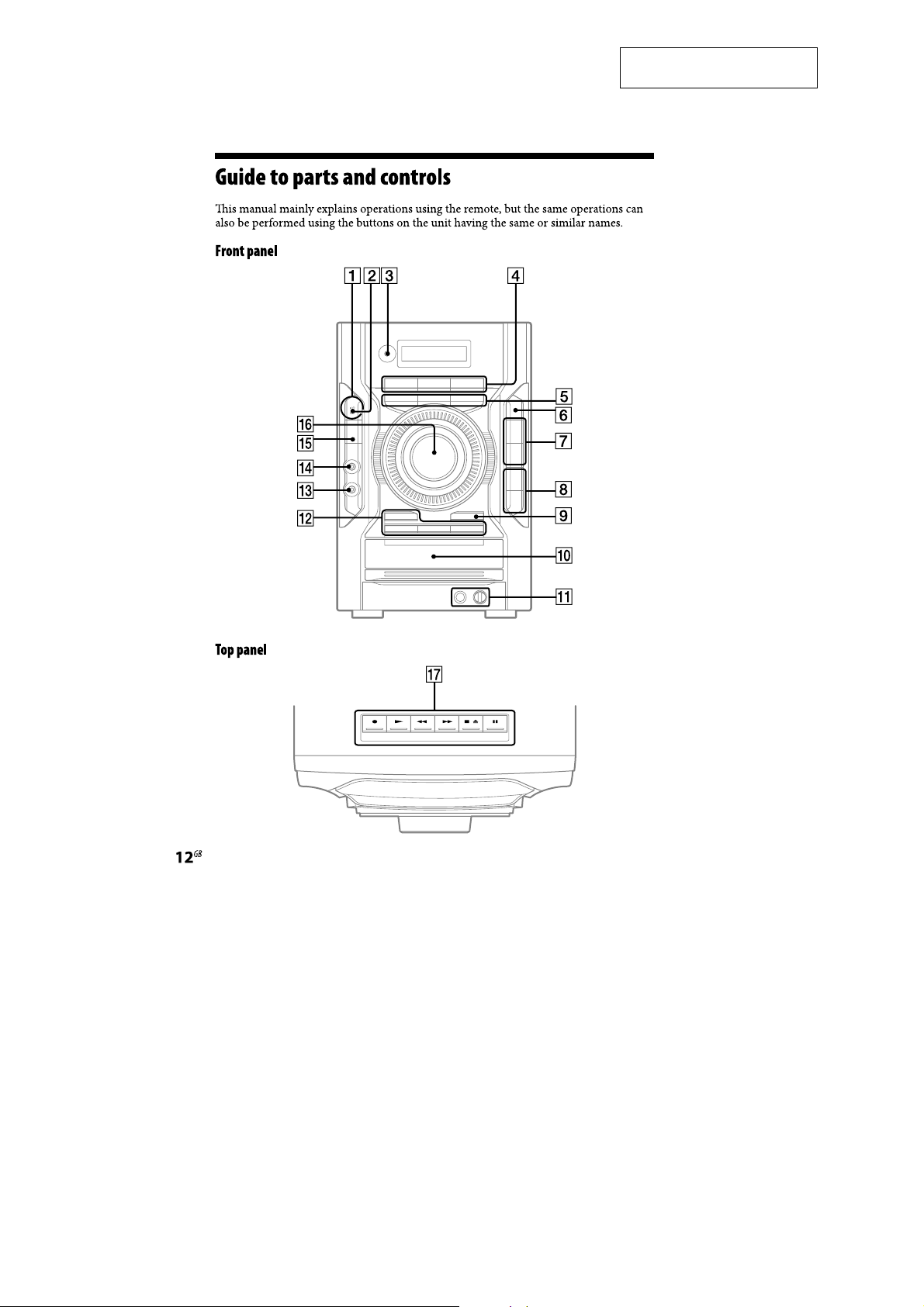
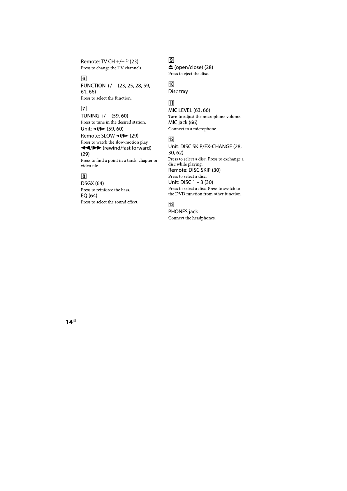
Guide to Parts and Controls............................................. 8
3. DISASSEMBLY
3-1. Side Panel (R), Side Panel (L) ......................................... 16
3-2. Top Panel Section ............................................................ 16
3-3. Door (CD) ........................................................................ 17
3-4. Front Panel Section ......................................................... 17
3-5. Main Board ...................................................................... 18
3-6. DC Fan ............................................................................ 18
3-7. Rear Panel ........................................................................ 19
3-8. AMP Board ...................................................................... 19
3-9. PT Board .......................................................................... 20
3-10. Cover (CDM)................................................................... 20
3-11. CD Mechanism Section................................................... 21
3-12. DMB16 Board ................................................................. 21
3-13. Belt (DLM3A)................................................................. 22
3-14. Optical Pick-up................................................................ 22
3-15. Mechanism Deck............................................................. 23
3-16. Belt (Main), Belt (R/F).................................................... 23
4. TEST MODE.............................................................. 24
5. MECHANICAL ADJUSTMENTS ....................... 28
6. ELECTRICAL ADJUSTMENTS ......................... 28
7. DIAGRAMS
7-1. Block Diagram – RF/Servo Section – ............................. 31
7-2. Block Diagram – Video Section – ................................... 32
7-3. Block Diagram – Main Section – .................................... 33
7-4. Block Diagram – Display Section –................................ 34
7-5. Printed Wiring Boards – Main Section –......................... 36
7-6. Schematic Diagram – Main Section (1/3) – .................... 37
7-7. Schematic Diagram – Main Section (2/3) – .................... 38
7-8. Schematic Diagram – Main Section (3/3) – .................... 39
7-9. Printed Wiring Board – DMB16 Section (1/2) –............. 40
7-10. Printed Wiring Board – DMB16 Section (2/2) –............. 41
7-11. Schematic Diagram – DMB16 Section (1/6) – ............... 42
7-12. Schematic Diagram – DMB16 Section (2/6) – ............... 43
7-13. Schematic Diagram – DMB16 Section (3/6) – ............... 44
7-14. Schematic Diagram – DMB16 Section (4/6) – ............... 45
7-15. Schematic Diagram – DMB16 Section (5/6) – ............... 46
7-16. Schematic Diagram – DMB16 Section (6/6) – ............... 47
7-17. Printed Wiring Board – AMP Section – .......................... 48
7-18. Schematic Diagram – AMP Section –............................. 49
7-19. Printed Wiring Board – Deck Section – .......................... 50
7-20. Schematic Diagram – Deck Section – ............................. 51
7-21. Printed Wiring Boards – MIC/Jack Section – ................. 52
7-22. Schematic Diagram – MIC/Jack Section –...................... 53
7-23. Printed Wiring Boards – Panel Section – ........................ 54
7-24. Schematic Diagram – Panel Section – ............................ 55
7-25. Printed Wiring Board – Power Section – ........................ 56
7-26. Schematic Diagram – Power Section – ........................... 57
8. EXPLODED VIEWS
8-1. Overall Section................................................................ 70
8-2. Front Panel Section ......................................................... 71
8-3. Main Board Section......................................................... 72
8-4. Rear Panel Section........................................................... 73
8-5. Chassis Section................................................................ 74
8-6. Top Panel Section............................................................ 75
8-7. DVD Mechanism Deck Section ...................................... 76
9. ELECTRICAL PARTS LIST................................ 77
5
Page 6
HCD-GNZ333D/GNZ444D
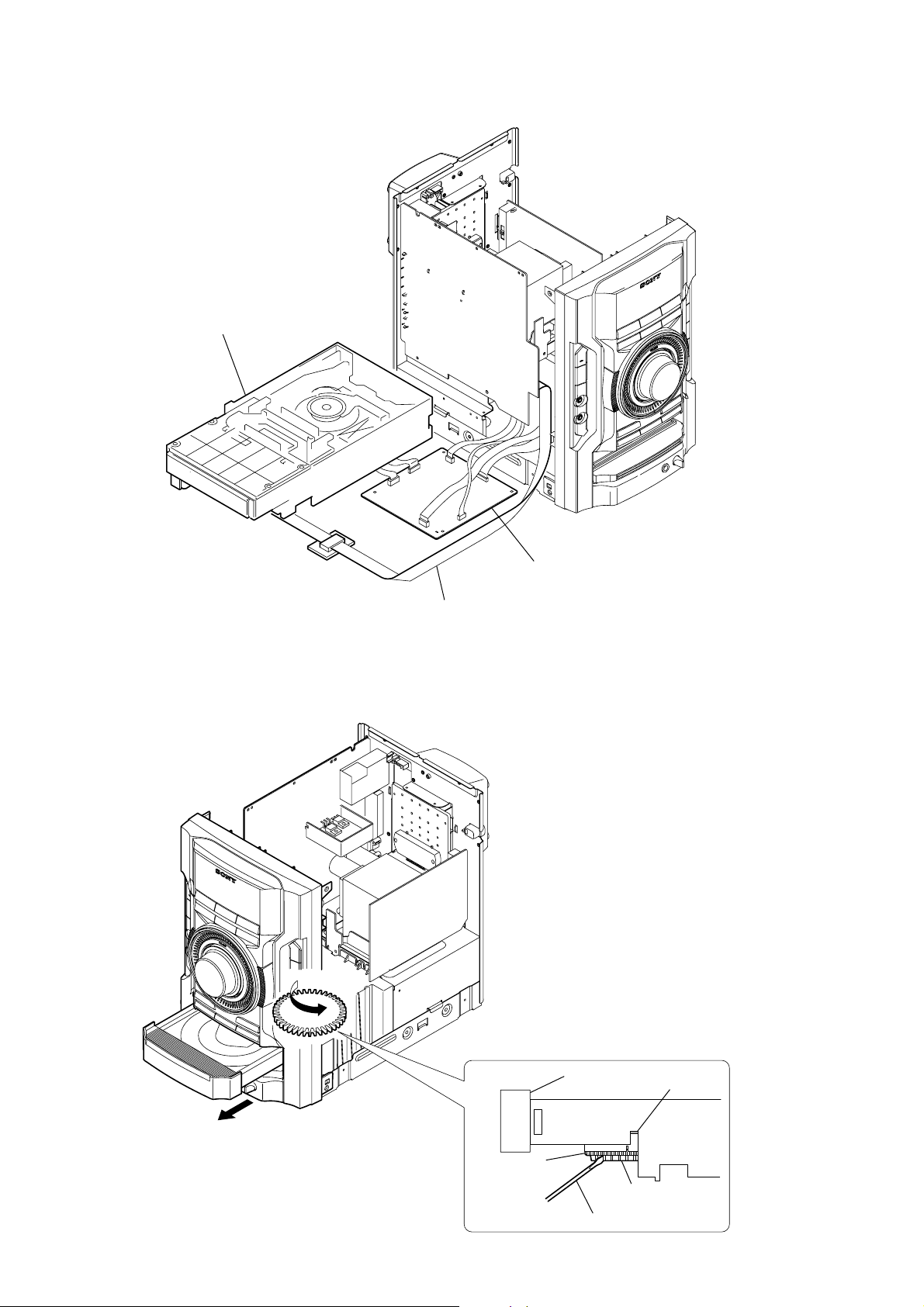
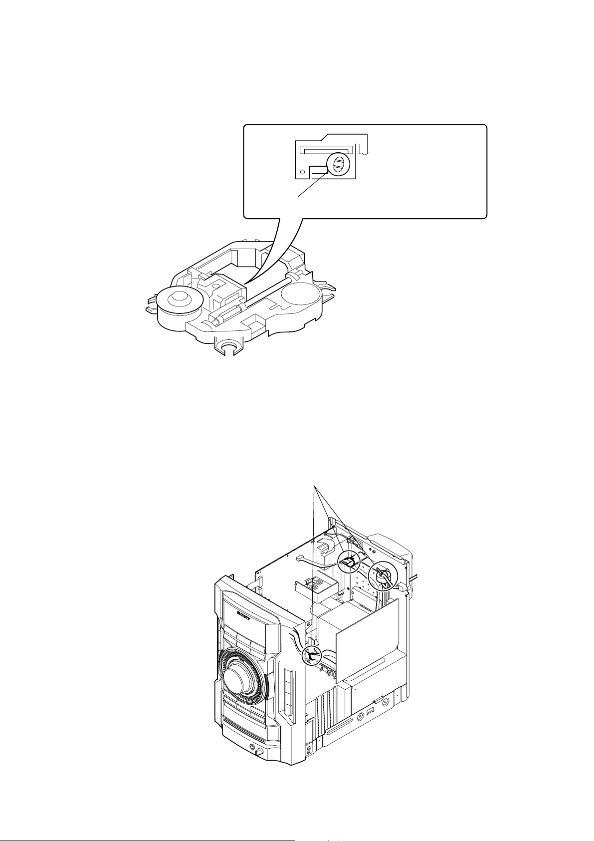
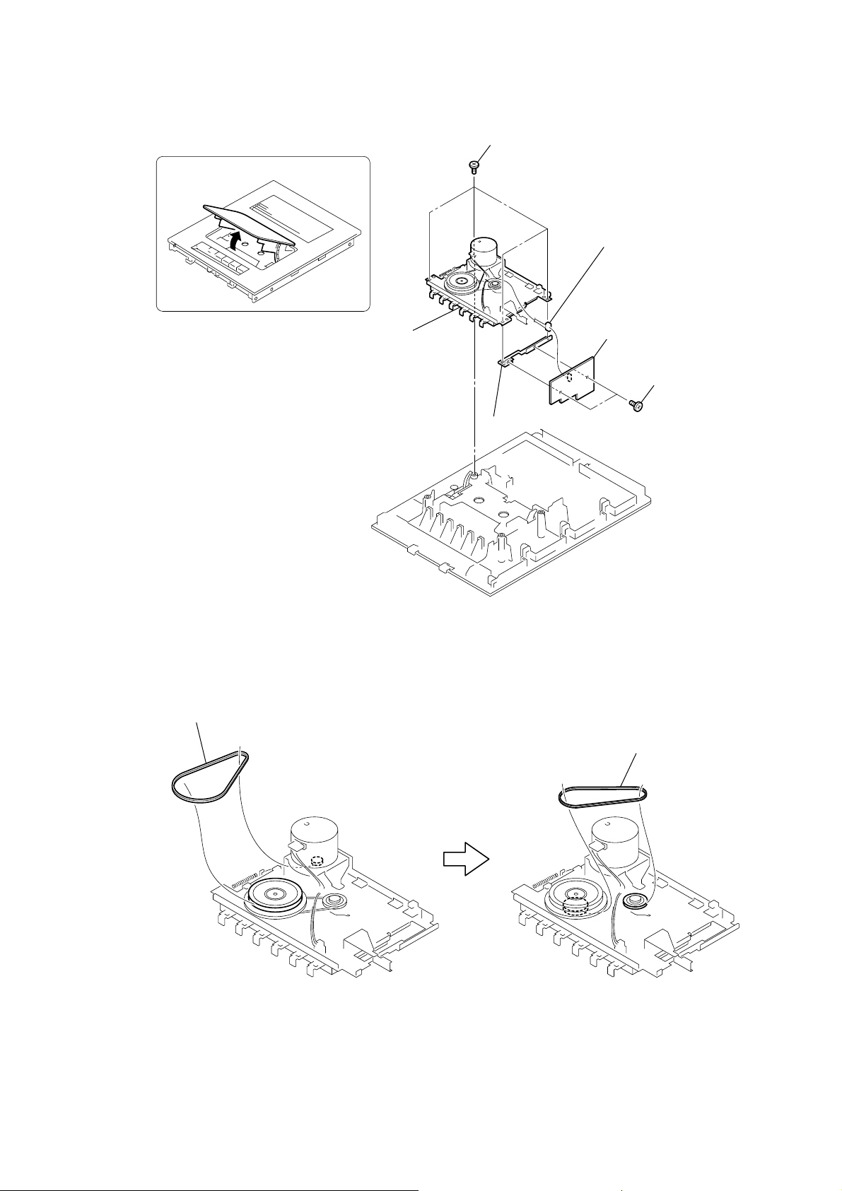
1. CDM SERVICE POSITION
CDM mechanism block
SECTION 1
SERVICING NOTES
2. OPENING THE CD TRAY MANUAL
A
J-2501-077-A
(1.25m/13P/300L)
1
DMB16 board
Turn the bottom rib (not the gear) with
a flathead screwdriver in the direction
of arrow A, with the lever pushed up,
draw out the door (CD) by the hand.
door (CD)
lever
gear
bottom rib
flathead screwdriver
6
Page 7
3. NOTE FOR HANDLING THE BU
HCD-GNZ333D/GNZ444D
Perform solder bridging to prevent damage
by electrostatic discharge when handling the BU as a single unit.
4. ARRANGEMENT OF THE CORD
cordes are fixed
7
Page 8
HCD-GNZ333D/GNZ444D
SECTION 2
GENERAL
This section is extracted from
instruction manual.
8
Page 9
HCD-GNZ333D/GNZ444D
9
Page 10
HCD-GNZ333D/GNZ444D
10
Page 11
HCD-GNZ333D/GNZ444D
11
Page 12
HCD-GNZ333D/GNZ444D
12
Page 13
HCD-GNZ333D/GNZ444D
13
Page 14
HCD-GNZ333D/GNZ444D
14
Page 15
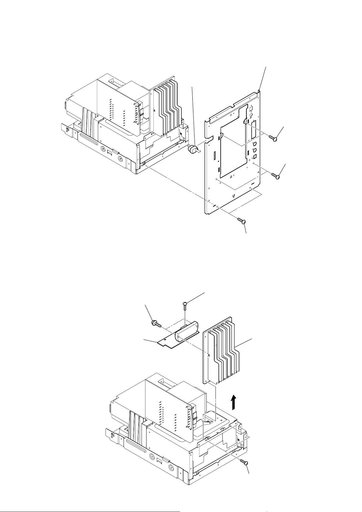
Note: Disassemble the unit in the order as shown below.
SET
3-1. SIDE PANEL (R),
SIDE PANEL (L)
(Page 16)
3-2. TOP PANEL SECTION
(Page 16)
HCD-GNZ333D/GNZ444D
SECTION 3
DISASSEMBLY
3-3. DOOR (CD)
(Page 17)
3-4. FRONT PANEL SECTION
(Page 17)
3-10. COVER (CDM)
(Page 20)
3-11. CD MECHANISM SECTION
(Page 21)
3-6. DC FAN
(Page 18)
3-7. REAR PANEL
(Page 19)
3-8. AMP BOARD
(Page 19)
3-9. PT BOARD
(Page 20)
3-5. MAIN BOARD
(Page 18)
3-15. MECHANISM DECK
(Page 23)
3-16. BELT (MAIN),
BELT (R/F)
(Page 23)
3-12. DMB16 BOARD
(Page 21)
3-14. OPTICAL PICK-UP
(Page 22)
3-13. BELT (DLM3A)
(Page 22)
15
Page 16
HCD-GNZ333D/GNZ444D
)
Note: Follow the disassembly procedure in the numerical order given.
3-1. SIDE PANEL (R), SIDE PANEL (L)
7
two
screws
(case 3 TP2)
6
two
screws
(case 3 TP2)
0
side panel (L)
9
8
(+BVTP 3
three
screws
×
10)
5
side panel (R)
3
(+BVTP 3
4
four
screws
×
10)
3-2. TOP PANEL SECTION
1
wire (flat type) (9 core)
(CN102)
4
two
screws
(+BVTP 3
3
screw
(+KTP 3
×
10)
×
10)
5
two
screws
(+BVTP 3
6
top panel section
2
two
(case 3 TP2
1
two
screws
(case 3 TP2)
×
10)
screws
16
2
screw
(+KTP 3
×
10)
Page 17
3-3. DOOR (CD)
4
door (CD)
tray
A
HCD-GNZ333D/GNZ444D
3
Turn the bottom rib (not the gear) with
a flathead screwdriver in the direction
of arrow A, with the lever pushed up,
draw out the door (CD) by the hand.
door (CD)
lever
3-4. FRONT PANEL SECTION
3
4
screw
(+BVTP 3
CN103 (4P)
×
10)
2
lid CDM cover
2
CN101 (8P)
lug
1
screw
(+BVTP 3
1
(CN402)
×
10)
wire (flat type) (15 core)
gear
bottom rib
flathead screwdriver
lug
7
front panel section
6
two
screws
(+BVTP 3
×
10)
5
screw
(+BVTP 3
×
10)
17
Page 18
HCD-GNZ333D/GNZ444D
)
3-5. MAIN BOARD
2
wire (flat type) (9 core)
(connector)
qa
screw
(+BVTP 3
qk
MAIN board
1
two
screws
(+BVTP 3
5
wire (flat type) (19 core)
(CN406)
×
10)
×
10)
qs
REG board
qj
CN105 (3P)
4
tuner (FM/AM)
(TN001)
8
CN107 (4P)
3
two
screws
(+BVTP 2.6
qd
five
(+BVTP 3
qf
CN751 (10P)
qg
CN001 (6P)
×
8)
screws
×
10
7
wire (flat type) (13 core)
(CN403)
3-6. DC FAN
9
CN401 (5P)
0
wire (flat type) (5 core)
(CN405)
6
wire (flat type) (13 core)
(CN404)
5
DC fan
qh
CN002 (8P)
6
cover (fan)
screw
1
(+BVTP 3
×
10)
18
3
4
two
(+BVTP 3
2
three
(+BVTP 3
screws
screws
×
10)
×
10)
Page 19
3-7. REAR PANEL
1
cord bushing (2104)
HCD-GNZ333D/GNZ444D
5
rear panel section
2
two
screws
(+BVTP 3
3
two
(+BVTP 3
screws
×
×
10)
10)
3-8. AMP BOARD
4
two
(transistor)
5
AMP board
screws
3
screw
(+BVTP 3
2
×
10)
4
two
screws
(+BVTP 3
6
heat sink assy
×
10)
1
two
screws
(+BVTP 3
×
10)
19
Page 20
HCD-GNZ333D/GNZ444D
3-9. PT BOARD
2
(+BVTT 4
two
screws
×
1
two
6)
screws
(+BVTT 4
3
PT board
×
6)
3-10. COVER (CDM)
7
F HOLD B board
6
F HOLD A board
8
ferrite core
9
two
(+BV 3 (3-CR))
5
two
screws
(+BVTP 2.6
screws
×
8)
4
FFC HOLD board
3
screw
(+BV 3 (3-CR))
0
two
screws
(+BV 3 (3-CR))
qa
cover (CDM)
1
screw
(+BVTP 3
2
lid CDM cover
×
10)
20
Page 21
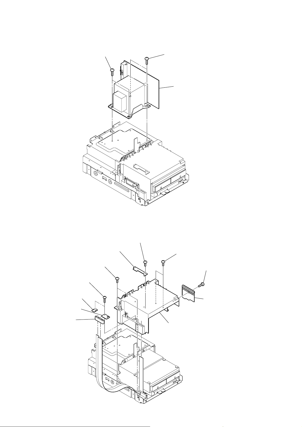
3-11. CD MECHANISM SECTION
5
two
screws
(+BV 3 (3-CR))
7
2
two
screws
(+BVTP 3
×
10)
6
two
screws
(+BV 3 (3-CR))
0
9
bracket (CDM)
8
two
(+BVTP 3
HCD-GNZ333D/GNZ444D
CD mechanism section
3
bracket (PT)
screws
×
10)
3-12. DMB16 BOARD
9
bracket (PWB DVD)
8
two
screws
(+BVTP 3
4
two
screws
(+BV 3 (3-CR))
×
10)
1
CN201 (6P)
two
screws
4
(+BVTP 3
2
(CN101)
×
10)
wire (flat type) (24 core)
6
(+BVTP 3
1
two
screws
(+BVTP 3
3
two
(+BV 3 (3-CR))
5
DMB board
two
×
10)
screws
screws
×
10)
7
WIRE PROTECT board
21
Page 22
HCD-GNZ333D/GNZ444D
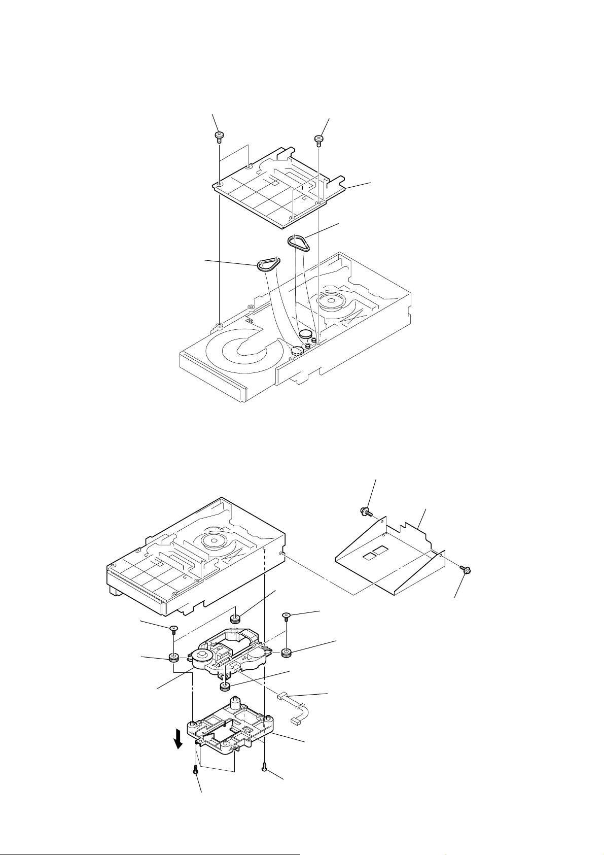
3-13. BELT (DLM3A)
5
belt (DLM3A)
1
two screws
2
two screws
4
3
cover
belt (DLM3A)
3-14. OPTICAL PICK-UP
0
two
screws
(insulator)
qa
insulator
qf
optical pick-up
6
qs
insulator
9
7
(insulator)
insulator
qg
bracket (BU)
two
8
qd
cord
2
(+PTPWHM 2.6)
screws
insulator
floating
screw
3
sheet (bottom)
1
floating
(+PTPWHM 2.6)
screw
22
5
three
(+BTP 2.6
screws
×
8)
4
two
screws
(+BTP 2.6
×
8)
Page 23
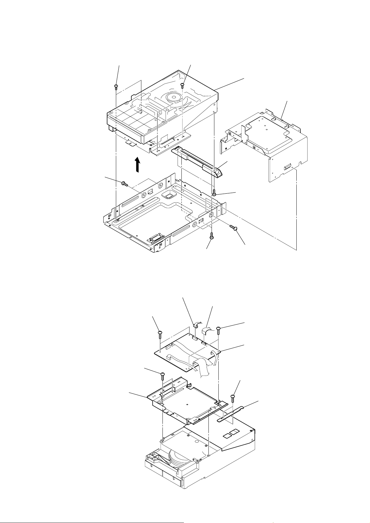
3-15. MECHANISM DECK
1
Open the cassette box.
7
mechanical deck
2
four screws
(+BVTP 2.6 × 8)
4
bracket (DECK)
HCD-GNZ333D/GNZ444D
5
connector
(CN501)
6
DECK board
3
two screws
(+BVTP 3 × 6)
3-16. BELT (MAIN), BELT (R/F)
1
belt (MAIN)
2
belt (R/F)
23
Page 24

HCD-GNZ333D/GNZ444D
SECTION 4
TEST MODE
[PANEL TEST MODE]
•This mode is used to check the LCD display, LEDs, keys,
VOLUME jog and OPERATION DIAL jog, model,
destination, software version and VACS level.
Procedure:
1. Press x button, [DISPLAY] button and X button simultaneously .
2. All LEDs and segments in LCD display are lighted up. All
LEDs are lighted up in red.
3. When you want to enter to the software version dispaly mode,
press [FUNCTION] button. The model inf ormation appears on
the fluorescent indicator tube. “GRL2D” is shown for HCDGNZ333D and “GRL4D” is shown for HCD-GNZ444D. Press
[DISC 1] button again to view the destination information.
4. Each time [DISC 1] button is pressed , the display changes from
MC version, SYS version, UI version, D VD version, CDMA
version, CDMB version, ST version, T A version, TM v ersion,
TC version in this order, and returns to the model information
display.
5. When [DISC 3] button is pressed while the version numbers
are being displayed except model and destination, the date of
the software creation appears. When [DISC 3] button is pressed
again, the display returns to the software version display . When
[DISC 1] button is pressed while the date of the software creation
is being displayed, the date of the software creation is displayed
in the same order of software version display.
6. Press [DISC 2] button, the key check mode is activated.
7. In the key check mode, the LCD displays “K 0 V0 J0”.
Each time a button is pressed, “K” value increases. However,
once a button has been pressed, it is no longer taken into
account.
“V” value increases in the manner of 0, 1, 2, 3 ... if [VOLUME]
knob is turned clockwise, or it decreases in the manner of 0,
9, 8, 7 ... if [VOLUME] knob is turned counterclockwise.
8. When [DISC SKIP/EX-CHANGE] button is pressed after all LEDs
and segments in LCD display light up, alternate segments in
LCD display would light up. If you press [DISC SKIP/EX-
CHANGE] button again, another half of alternate segments in
LCD display would light up. When [DISC SKIP/EX-CHANGE]
button is pressed again, all segments lights off. Press [DISC
SKIP/EX-CHANGE] button again would cause all segments
lights up.
9. To release from this mode, disconnect the AC plug.
[DVD SHIP MODE]
•This mode can run the DVD sled motor optionally. Use this
mode, for instance, when cleaning the optical pick-up.
Procedure:
1. Press the
2. Press the [FUNCTION] button to select DVD function.
3. Press two buttons of DVD N and @/1 simultaneously.
4. Set to the DVD ship mode. (chucking on)
5. After blink “STANDBY”, “LOCK” is displayed, disconnect
the AC plug.
[COLD RESET]
• The cold reset clears all data including preset data stored in
the RAM to initial conditions. Execute this mode when
returning the set to the customer.
Procedure:
1. Press @/1 button to turn on the system.
2. Press x button, [TUNER/BAND] button, and @/1 STANDBY
button simultaneously.
3. The message “RESET” appears on the LCD display. Then,
the LCD display becomes blank for a while, and the system is
reset.
[TUNER STEP CHANGE]
•The step interval of AM channels can be toggled between 9
kHz and 10 kHz. This mode is not available for Saudi Arabia
and Russia models.
Procedure:
1. Press @/1 button to turn on the system.
2. Press [TUNER/BAND] button repeatedly to select the “AM”.
3. Press
4. After pressing the [DISPLAY] button, press [PRESET +] button
and @/1 STANDBY button simultaneously. The system will
turn on automatically. The message “AM 9K STEP” or “AM
10K STEP” appears on the LCD display and thus the channel
step is changed.
[DVD POWER MANAGE]
•This mode is for switch the DVD power supply on/off. Even
if this state pulls out AC plug, it is held.
@/1 button to turn the power on.
@/1 button to turn off the system.
[REPEAT 5 LIMIT OFF MODE]
• Number of repeats for DVD playback is 5 times when the
repeat mode is “REPEA T”. This mode enables DVD to repeat
playback for limitless times.
Procedure:
1. Press the @/1 button to turn the power on.
2. Press the [FUNCTION] button to select DVD function.
3. Press three buttons of DVD N , [DSGX], and [DISPLAY]
simultaneously.
4. It enters the DVD repeat 5 limit cancel mode and displays
“NO LIMIT”.
5. To release this mode, press three buttons of DVD N , [DSGX],
and [DISPLAY] simultaneously.
24
Procedure:
1. Press the @/1 button to turn the power on.
2. Press the [FUNCTION] button to select DVD function.
3. Press the @/1 button again to turn the power off (standby).
4. After pressing the [DISPLAY] button, press two buttons of
DVD N and @/1 simultaneously.
5. It turns power on and display “DVD POWER”, then display
“ON” or “OFF”.
[DVD SHIP MODE]
•This mode moves the optical pick-up to the position durable
to vibration. Use this mode when returning the set to the
customer after repair.
Procedure:
1. Press @/1 button to turn on the system.
2. Select DVD function.
3. Press DVD N button and @/1 button simultaneously during
“DVD NO DISC” condition. The system will turn off
automatically.
4. After the “STANDBY” blinking display finishes, a message
“MECHA LOCK” appears on the LCD display and the DVD
ship mode is set.
Page 25
HCD-GNZ333D/GNZ444D
Ver. 1.1
[DVD SHIP AND COLD RESET]
Procedure:
1. Press the @/1 button to turn the power on.
2. Press the [FUNCTION] button to select DVD function.
3. Press three buttons of [FUNCTION], DVD N and @/1
simultaneously.
4. After blink “ST ANDBY”, “RESET” is displayed, disconnect
the AC plug.
[DVD SLOT LOCK]
•This mode is for the antitheft of DVD disc in shop. (not for
transport)
Procedure:
1. Press the @/1 button to turn the power on.
2. Press the [FUNCTION] button to select DVD function.
3. Insert a disc.
4. While pressing the x button, press the Z button for more 5
seconds.
5. The message “LOCKED” is displayed and the disc slot is
locked. (Even if exiting from this mode, the disc slot is still
locked)
6. If press the Z button to eject the disc, the message “LOCKED”
is displayed and can not eject the disc.
7. To release this lock, while pressing the x button, press the
Z button for 5 seconds again.
8. The message “UNLOCKED” is displayed and the disc slot is
unlocked.
• Procedure to enter to DVD Service Mode:
1. Press
@/1 button to turn on the system.
2. Select DVD function.
3. Press
DVD N button and Z button simultaneously and then
turn the [VOLUME] knob clockwise.
4. The message “SERVICE IN” appears on the LCD display and
the Top Menu of Remocon Diagnosis Menu appears on the
on-screen display on the TV. The model name, main unit’s
micom version information (IF-con) and DVD firmware
version information (Syscon) are displayed at the bottom of
the on-screen display.
Remocon Diagnosis Menu
0. External Chip Check
1. Servo Parameter Check
2. Drive Manual Operation
3. Emergency History
4. Version Information
Model Name : EROD_ME
IF-con : V
Syscon : Ver.
er. 01.00 (0000)
1.200
5. To execute each function, press its number by using numeric
button on the remote commander.
6. To release from this mode, press
@/1 button to turn off the
system.
[DVD COLOR SYSTEM] (EXCEPT E13 MODEL)
• This mode let you change the color system of the video output
from PAL to NTSC or vice-versa. This mode is not available
for Latin American and Russian models.
Procedure:
1. Press
@/1 button to turn on the system.
2. Select DVD function.
3. Press @/1 button again to turn off the system.
4. After pressing the [DISPLAY] button, press X button and @/1
button simultaneously . The system will turn on automatically .
The message “COLOR P AL” or “COLOR NTSC” appears on
the LCD display.
[DVD SERVICE MODE]
•This mode let you make diagnosis and adjustment easily by
using the remote commander and the TV. The instructions,
diagnostic results, etc. are given on the on-screen display.
• TEST DISC LIST
Be sure to use the DVD disc that matches the signal standards of
your region.
• CD
YEDS-18 (Part No.: 3-702-101-01)
PATD-012 (Part No.: 4-225-203-01)
• DVD SL (Single Layer)
NTSC : HLX-503 (Part No.: J-6090-069-A)
HLX-504 (Part No.: J-6090-088-A)
PAL:HLX-506 (Part No.: J-6090-077-A)
• DVD DL (Dual Layer)
NTSC : HLX-501 (Part No.: J-6090-071-A)
HLX-505 (Part No.: J-6090-089-A)
PAL:HLX-507 (Part No.: J-6090-078-A)
• Execute IOP Measurement
In order to execute IOP measurement, the following standard
procedures must be followed.
1. From the Top Menu of Remocon Diagnosis Menu, select “2.
Drive Manual Operation” by pressing the [2] button on the
remote commander. The following screen appears on the onscreen display.
Drive Manual Operation
1. Servo Control
2. Track/Layer Jump
3. Manual Adjustment
4. Mecha test Mode
5. MIRR time Adjust
0. Return to Top Menu
2. Select “3. Manual Adjustment” by pressing the [3] button on
the remote commander. The following screen appears on the
on-screen display.
Manual Adjust
1. Track Balance Adjust:
2. Track Gain Adjust:
3. Focus Balance Adjust:
4. Focus Gain Adjust:
5. Eg Boost Adjust:
6. Iop:
7. TRV. Level:
8. S curve(FE) Level:
9. RFL(PI) Level:
0. MIRR Time:
O o Change Value
RETURN Return to previous menu
25
Page 26
HCD-GNZ333D/GNZ444D
Ver. 1.1
3. Select “6. Iop:” by pressing [6] button on the remote
commander.
4. Wait until a hexadecimal number appears in the on-screen
display as below:
Manual Adjust
1. Track Balance Adjust:
2. Track Gain Adjust:
3. Focus Balance Adjust:
4. Focus Gain Adjust:
5. Eg Boost Adjust:
6. Iop. ED:
7. TRV. Level:
8. S curve(FE) Level:
9. RFL(PI) Level:
0. MIRR Time:
O o Change Value
RETURN Return to previous menu
5. Convert data from hexadecimal to decimal by using con version
table.
6. Please find the label on the rear of the BU (Base Unit).
The default IOP value is written in the label.
7. Subtract between these two values.
8. If the remainder is smaller than 93 (decimal), then it is OK.
However if the v alue is higher than 93, then the BU is defective
and need to be change.
9. Press [RETURN] button on the remote commander to return to
previous menu.
10. Press [0] button on the remote commander to retur n to the T op
Menu of Remocon Diagnosis Menu.
11. Press
@/1 button to turn off the system.
• Error Code
Example of Error code
1. 01 05 04 04 00 92 46 00
00 00 00 00 00 00 23 45
The meaning of error code is as below:
01: Communication error (No reply from syscon)
02: Syscon hung up
03: Power OFF request when syscon hung up
19: Thermal shutdown
24: MoveSledHome error
25: Mechanical move error (5 Changer)
26: Mechanical move stack error
30: DC motor adjustment error
31: DPD offset adjustment error
32: TE balance adjustment error
33: TE sensor adjustment error
34: TE loop gain adjustment error
35: FE loop gain adjustment error
36: Bad jitter after adjustment
40: Focus NG
42: Focus layer jump NG
52: Open kick spindle error
51: Spindle stop error
60: Focus on error
61: Seek fail error
62: Read Q data/ID error
70: Lead in data read fail
71: TOC read time out (CD)
80: Can’t buffering
81: Unknown media type
• Check Emergency History
To check the emergency history, please follow the following
procedure.
1. From the Top Menu of Remocon Diagnosis Menu, select “3.
Emergency History” by pressing the [3] button on the r emote
commander. The following screen appears on the on-screen
display.
Emg. History Check
Laser Hours CD 999h 59min
1. 01 05 04 04
00 00 00 00 00 00 23 45
2. 02 02 01 01 00 A9 4B 00
00 00 00 00 00 00 23 45
Next Next Page Prev Prev Page
O Return to Top Menu
DVD 999h 59min
00 92 46 00
2. Y ou can check the total time when the laser is turned on during
playback of DVD and CD from the above menu. The maximum
time, which can be displayed are 999h 59min.
3. You can check the error code of latest 10 emergency history
from the above menu. To view the previous or next page of
emergency history, press . or > on the remote
commander. The error code consists of
•Parameter of error code
This is the detail of error code.
Example of Error code
1. 01 05 04 04 00 92 46 00
00 00 00 00 00 00 23 45
• Time of error code
This is the laser time when an error occurred.
Example of Error code
1. 01 05 04 04 00 92 46 00
00 00 00 00 00 00 23 45
26
Page 27
HCD-GNZ333D/GNZ444D
Ver. 1.1
To clear the Laser Hour
Press [DISPLAY] button and then press [CLEAR] button. The data
for both CD and DVD data are reset.
Emg. History Check
Laser Hours CD 0h 0min
1. 01 05 04 04
00 00 00 00 00 00 23 45
2. 02 02 01 01 00 A9 4B 00
00 00 00 00 00 00 23 45
Next Next Page Prev Prev Page
O Return to Top Menu
DVD 0h 0min
00 92 46 00
To clear the Emergency History
Press [DVD TOP MENU] button and then press [CLEAR] button. T he
error code for all emergency history would be reset.
Emg. History Check
Laser Hours CD 999h 59min
1. 00 00 00 00
00 00 00 00 00 00 00 00
2. 00 00 00 00 00 00 00 00
00 00 00 00 00 00 00 00
Next Next Page Prev Prev Page
O Return to Top Menu
DVD 999h 59min
00 00 00 00
To return to the Top Menu of Remocon Diagnosis Menu
Press [0] button on the remote commander.
• Check Version Information
To check the version information, please follow the following
procedure.
1. From the Top Menu of Remocon Diagnosis Menu, select “4.
Version Information” by pressing the [4] button on the remote
commander. The following screen appears on the on-screen
display.
Version information
Firm (Main) : Ver. xxxxx
Firm (Sub) : xxxxx
RISC : xxxxx
8032 : xxxxx
Audio DSP : xxxxx
Servo DSP : xxxxx
O Return to Top Menu
To return to the T op Menu of Remocon Diagnosis Menu, press
[0] on the remote commander.
To clear the Initialize Setup Data
Press [DVD/TUNER MENU] button and then press [CLEAR] button
on the remote commander.
Emg. History Check
Laser Hours CD 999h 59min
Initialize setup data...
Next Next Page Prev Prev Page
O Return to Top Menu
DVD 999h 59min
27
Page 28
HCD-GNZ333D/GNZ444D
set
JACK board
PHONES jack
(J252)
+
–
level meter
test tape
P-4-A063
(6.3 kHz,
−
10 dB)
SECTION 5
MECHANICAL ADJUSTMENTS
SECTION 6
ELECTRICAL ADJUSTMENTS
• Precaution
1. Clean the following parts with a denatured-alcohol-moistened
swab :
record/playback head pinch roller
erase head rubber belts
capstan idlers
2. Demagnetize the record/playback head with a head
demagnetizer. (Do not bring the head magnetizer close to the
erase head.)
3. Do not use a magnetized screwdriver for the adjustments.
4. After the adjustments, appiy suitable locking compound to
the parts adjusted.
5. The adjustments should be performed with the rated power
supply voltage unless otherwise noted.
• Torque Measurement
Mode
FWD
FWD
back tension
FF
REW
Torque meter
CQ-102AS
CQ-102C
CQ-201AS
CQ-201B
Meter reading
2.0 – 8.0 mN • m
(20 to 80 g • cm)
(0.28 – 1.12 oz • inch)
0.15 – 0.6 mN • m
(1.5 to 6 g • cm)
(0.021 – 0.083 oz • inch)
5 – 17.7 mN • m
(50 to 177 g • cm)
(0.7 – 2.48 oz • inch)
5 – 17.7 mN • m
(50 to 177 g • cm)
(0.7 – 2.48 oz • inch)
DECK SECTION
0 dB=0.775 V
1. Demagnetize the record/playback head with a head
demagnetizer.
2. Do not use a magnetized screwdriver for the adjustments.
• Test T ape
Tape Signal Used for
P-4-A063 6.3 kHz, –10 dB Azimuth Adjustment
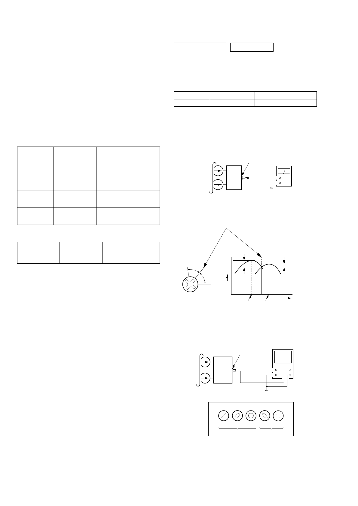
RECORD/PLAYBACK HEAD AZIMUTH ADJUSTMENT
Procedure:
1. Mode: Playback
2. Turn the adjustment scre w and check output peaks. If the peaks
do not match for L-CH and R-CH, turn the adjustment screw
so that outputs match within 1dB of peak.
• Tape T ension Measurement
Mode Tension Meter Meter Reading
FWD CQ-403A
(more than 2.82 oz)
more than 80 g
L-CH
peak
Output
level
R-CH
Screw
position
peak
3. Mode: Playback
test tape
P-4-A063
(6.3 kHz, −10 dB)
within
1dB
L-CH
peak
JACK board
PHONES jack
(J252)
set
waveform of oscilloscope
R-CH
peak
within
1dB
oscilloscope
H
V
Screw
position
28
in phase 45°90°135°180
good
°
wrong
4. After the adjustments, apply suitable locking compound to
the pats adjusted.
Page 29

HCD-GNZ333D/GNZ444D
signal
generator
OUTPUT
(75
Ω
)
set
Adjustment Location: Record/Playback/Erase Head
TUNER SECTION
[FM TUNE LEVEL CHECK]
Procedure:
1. Turn on the set.
2. Input the following signal from signal generator to FM antenna
input directly.
Carrier frequency: A = 87.5 MHz, B = 98 MHz, C = 108 MHz
Deviation : 75 kHz
Modulation : 1 kHz
ANT input : 35 dBu (EMF)
Note: Use 75 ohm coaxial cable to connect signal generator and the set.
You cannot use video cable for checking.
Use signal generator whose output impedance is 75 ohm.
3. Set to FM tuner function and tune A, B and C signals.
4. Confirm “TUNED” is lit on the display for A, B and C signals.
When the selected station signal is received in good condition,
“TUNED” is displayed.
29
Page 30

HCD-GNZ333D/GNZ444D
Ver. 1.1
DVD SECTION
When the optical pick-up assy is replaced, perform the “Execute
IOP Measurement”.
Execute IOP Measurement (See page 25)
[TEST DISC LIST]
Be sure to use the DVD disc that matches the signal standards of
your region.
• CD
YEDS-18 (Part No.: 3-702-101-01)
PATD-012 (Part No.: 4-225-203-01)
• DVD SL (Single Layer)
NTSC : HLX-503 (Part No.: J-6090-069-A)
HLX-504 (Part No.: J-6090-088-A)
PAL:HLX-506 (Part No.: J-6090-077-A)
• DVD DL (Dual Layer)
NTSC : HLX-501 (Part No.: J-6090-071-A)
HLX-505 (Part No.: J-6090-089-A)
PAL:HLX-507 (Part No.: J-6090-078-A)
[RFMON Level Check]
Connection:
oscilloscope
DMB16 board
CN105 pin 6 (RFMON)
CN105 pin
3
(GND)
+
–
Checking Location: DMB16 board (Side A)
DMB16 BOARD
(SIDE A)
CN105
1
6
CN105 pin 3 (GND)
CN105 pin
IC104
IC101
IC102
6
(RFMON)
VIDEO SECTION
Video Level Check (MAIN BOARD)
Purpose
This adjustment is made to satisfy the NTSC standard, and if not
adjusted correctly, the brightness will be too large or small.
Procedure:
1. Connect an oscilloscope to CN105 pin 6 (RFMON) and
CN105 pin 3 (GND) on the DMB16 board.
2. Turn the power on.
3. Set the test disc (refer to the TEST DISC LIST) on the tray
and press DVD N button to playback.
4. Confirm that oscilloscope waveform is clear and check
RFMON signal level is correct or not.
Note: A clear RFMON signal waveform means that the shape “◊” can be
clearly distinguished at the center of the waveform.
RFMON signal waveform
VOLT/DIV: 200 mV
TIME/DIV: 500 ns
level: 0.58 ± 1.23 Vp-p (DVD)
0.57 ± 1.1 Vp-p (CD)
oscilloscope
75
Ω
set
J701
VIDEO OUTPUT
Procedure:
1. Connect oscilloscope to VIDEO output.
2. Load a DVD reference disc playback.
3. Check the video signal level is 1.00 ± 0.07Vp-p.
(WHITE 100%)
1.00 ± 0.07 Vp-p
30
Page 31

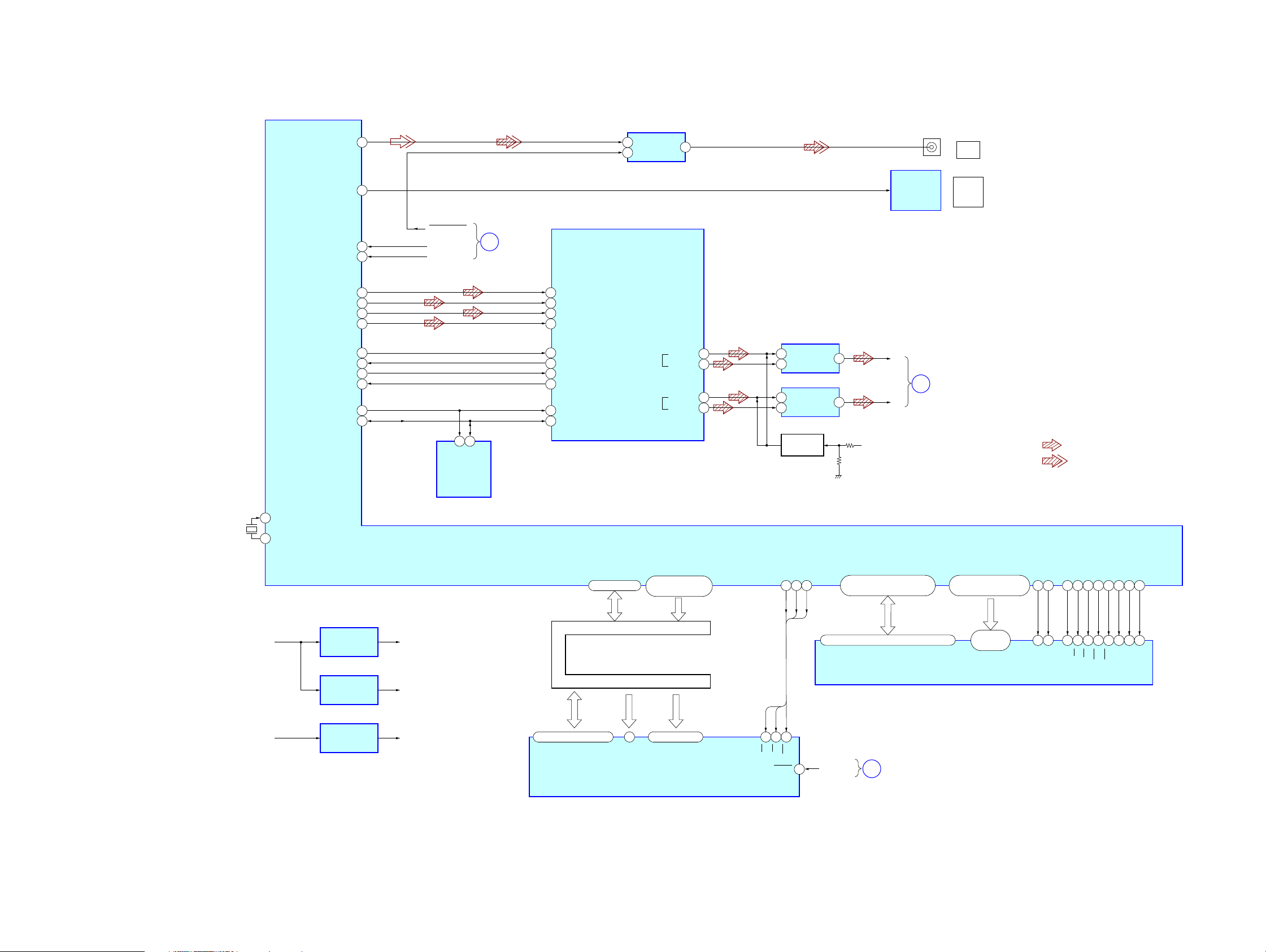
SECTION 7
DIAGRAMS
7-1. BLOCK DIAGRAM – RF/SERVO Section –
RF
6
DVDRFIP
V2REFO
RXD
TXD
HCD-GNZ333D/GNZ444D
CN105
6
RFMON
28
106
107
5
2
1
TEST PIN
V2REFO
RXD
TXD
DETECTOR
OPTICAL PICK-UP
BLOCK
LASER
DIODE
(FOR CD)
LASER
DIODE
(FOR DVD)
(LIMIT)
2AXIS
DEVICE
FOCUS/
TRACKING
COIL
MM
SLED
MM
SPINDLE
VC
CD LD
PD
DVD LD
VR650
VR780
MSW
FCS+
FCS–
TRK+
TRK–
SL–
SL+
SP+
SP–
A
B
C
D
F
E
AUTOMATIC POWER
CONTROL (FOR CD)
Q102 (1/2)
AUTOMATIC POWER
CONTROL (FOR DVD)
Q102 (2/2)
VOLUME CONTROL
Q101
B
A
C
D
IOP
Q103
2
DVDA
3
DVDB
4
DVDC
5
DVDD
19
TPI
18
TNI
A
8
NA
B
9
NB
C
10
MC
D
11
MD
29
V2O
23
LD01
20
MDI2
MDI1
21
LD02
22
MSW
50
LIMSW
176
FOCUS/TRACKING COIL DRIVER,
SPINDLE, SLED MOTOR DRIVER
42
36 48
37 1
35 3
34 4
SW+5V
SVCC
44
30
29
27
28
46
47
IC201
BUFFER
FOCUS COIL
DRIVE
TRACKING COIL
DRIVE
SLED MOTOR
DRIVE
SPINDLE MOTOR
DRIVE
BUFFER
CD/DVD RF AMP,
FOCUS/TRACKING ERROR AMP
DVD SYSTEM PROCESSOR
DIGITAL SERVO PROCESSOR
IC102(1/2)
43
10
13
40
45
19
20
22
21
VREFO
FOO
TRO
FMO
DMO
VREFO
FMO
FOO
DMO
TRO
246
38
42
37
41
30
40
47
211
210
170
REFPAC
FMO
FOO
DMO
TRO
VREFO
IOPMON
SPFG
MUTE123
MUTE
TSDM
PRST
IFCK
IFSDO
IFSDI
XIFCS
IFBSY
KRMOD/HSYNC
MIC/VSYNC
SYSRESET
VIDEO
C
SECTION
(Page 32)
110
99
98
101
100
105
207
205
42
O-MTK-MTRST
46
I-MTK-CLK
45
I-MTK-DATA
44
O-MTK-DATA
43
I-DVD-XIFCS
41
O-MTK-IFBSY
39
I-DVD-KRMOD
40
O-MTK-MICREQ
SYSTEM
CONTROL
IC401(1/3)
• Signal Path
: AUDIO(DVD)
: VIDEO(DVD)
HCD-GNZ333D/GNZ444D
3131
Page 32
HCD-GNZ333D/GNZ444D
7-2. BLOCK DIAGRAM – VIDEO Section –
198
YUV3
VIDEO OUT BUFFER
IC701
IN
4
1
OUT
PS
J701
2
VIDEO
OUT
X101
27MHz
225
SPDIF
D/A CONVERTER
VIDEO MUTE
206
VOICE
208
SMSCK
217
ASDAT0
218
ASDAT1
219
ASDAT2
222
ASDAT4
220
XRST
215
ACLK
214
ABCK
213
ALRCK
102
SCL
103
SDA
229
XTALI
XTALO
228
VOICE
SCORE
6 5
SCL
EEPROM
IC103
SDA
B
(Page 33)
MAIN
SECTION
14
SDTI1
15
SDTI2
16
SDTI3
13
SDTI4
8
PDN
10
MCLK
9
BICK
17
LRCK
19
SCL
20
SDA
DVD SYSTEM PROCESSOR
IC102(2/2)
HD0 – HD7 A0 – A21
IC301
AD0 – AD7
81-84,86-88,91
(DMIXL)
LOUT4+
LOUT4–
LOUT1+
(FL)
LOUT1–
HIGHA0-7
IOA0-7, IOA18-IOA21
A16, A17
53-61, 67-72, 74-76,
78, 89, 92, 93
IC3771
38
37
2
1
(+2.5V)
3
2
3
2
A +IN
A –IN
A +IN
A –IN
IOCS
77
CEWEOE
IC3711
DC BIAS
Q3801
IODE
79
66
A OUT
A OUT
IOWR
1
1
AU+5V
RD0 – RD15
125-123, 121, 120, 118,
117, 115, 135, 133-128, 126
OPTICAL
TRANSMITTER
IC555
LT
A
FL
DIGITAL
MAIN
SECTION
(Page 33)
158-160, 162, 164-166
DVD
OUT
RA0 – RA11
146, 147, 149-151,
• R-ch is omitted due to same as L-ch.
• Signal Path
: AUDIO (DVD)
: VIDEO (DVD)
RCLK
RCS
RWE
RAS
CAS
DQM0
DQM1
BA0
BA1
142
138
140
143
145 156 113 137 157
139
CKE
HCD-GNZ333D/GNZ444D
SW+5V
SW+3.3V
+3.3V REG
IC105
RF+3.3V REG
IC107
RF+1.8V REG
IC106
+3.3V
(DAVDD)
RF+3.3V
RF+1.8V
DATA & ADDRESS BUS
DATA & ADDRESS BUS
HD0 – HD7
29,31,33,35,38,40,42,44 25-16, 10 -1, 48
DQ0 – DQ7
A0
FLASH ROM
IC101
A0 – A19DQ15/A-1
3232
A1-A21
2,4,5,7,8,10,11,13,42,44,45,47,48,50,51,53
RD0 – RD15
CE
OE
WE
2645
28OE11
CE
WE
RESET
SYSRESET
12
C
RF/SERVO
SECTION
22-26,
29-35
RA0 – RA11
SDRAM
IC104
38
19
16
18
17
15
39
CAS
LDQM
37
UDQM
CKE
20
21
CS
WE
CLK
BS0
BS1
RAS
(Page 31)
Page 33

7-3. BLOCK DIAGRAM – MAIN Section –
+9V
J261
MIC
TAPE MECHANS DECK
REC/PB HEA
L-CH
R-CH
ERASE
HEAD
(PLAY)
CAPSTAN
MOTOR
(MOTOR)
VIDEO
A
SECTION
(Page 32)
VIDEO
B
SECTION
(Page 32)
J251
AUDIO IN
MM
VIDEO MUTE
LT
FL
SCORE
XVOICE
R-CH
+9V
R-CH
S501
(REC/PB)
MIC MUTE
Q261
–IN
2
L501
AUDIO (REC) SELECT
IC105
14
X1
15
X2
11
X3
KARAOKE SCORE
IC552, IC553, IC554
RV261
MIC
LEVEL
OUT OUT
PB AMP
IC501
5
IN+
REC AMP
IC502
7
OUT
REC
BIAS
OSC
Q501,502
X0
X
A
B
1
7
OUT
5
IN+
12
13
10
9
Q561
Q560
5 7
REC MUTE
Q103
BUFFER
Q102
MIC AMP
IC261
+IN
Q558
MIC MIX
–IN
2
+IN
3
MIC-DETECT
REC-MUTE
TP-STATE
REC-SEL-A
REC-SEL-B
VIDEO-MUTE
IC103
OUT
1 9
INPUT FUNCTION
VOL-L
AUDIO-L
5
TAPE-L
4
OUT-L
8
CD-L
7
CONTROL
IC101
L-OUT
DATA
CLK
HCD-GNZ333D/GNZ444D
R-CH
BASS BOOST
AMP
IC102
27
SWITCH
Q105,107
22
21
Q562
BB-ON
3
R-CH
+IN
1
OUT
O-BASSBOOST-ON
38
O-VOL-DATA
36
O-VOL-CLK
37
B+ SWITCH
Q555
REG+9V
SYSTEM CONTROL
IC401 (2/3)
POWER AMP
IC751
11
LI+
13
ST-BY
I-HP-DETECT
O-AMP-ON
5
LO–
4
LO+
+VP–VP
TH751
TEMPERATURE
PROTECT
77
32
PROTECT
Q753
PROTECT
LATCH
Q751,752
D752
D555
R-CH
DC OFFSET
DETECT
Q013,014
RELAY
DRIVER
Q551
HP-DETECT
AMP-ON
O-POWER
PROTECT
AMP-ON
HP-DETECT
DISPLAY
D
SECTION
(Page 34)
D556
UNREG (+16V)
FAN
CONTROL
Q552,554
FAN
PROTECT
Q556
+
–
+
–
+
MM
–
TB101
L
SPEAKER
IMPEDANCE:
USE 6Ω
R
GNZ444D
J603
SUB WOOFER
OUT
FAN 001
FAN
MOTOR
J252
PHONES
ANTENNA
FM 75Ω
COAXIAL
AM
HCD-GNZ333D/GNZ444D
TN001
TUNER
UNIT
DO/ST/SD
MIC-DETECT
REC-MUTE
L
R
SD
CE
DI
CL
R-CH
TU-SD
TU-CE
TU-DO
TU-CLK
TU-SI
6
TUNER-L
TP-STATE
REC-SEL-A
REC-SEL-B
VIDEO-MUTE
TU-SD
TU-CE
TU-DO
TU-CLK
TU-SI
I-MIC-DETECT
76
O-REC-MUTE
33
I-TP-STATE
58
O-REC-CONTROL-A
34
O-REC-CONTROL-B
35
O-VIDEO-MUTE
82
I-SD
31
O-TU-CE
29
O-TU-DO
28
O-TU-CLK
27
I-TU-DI
26
I-AC-CUT
RESET
SI/SO
FLMD0
10
Q493
90
89
93
RESET
Q463,464
CN410
4
5
1
–RESET
SI-SO (SERVICE)
FLMD0
RESET
IC402
1
OUT
VDD
2
VCC
(IC401)
• R-ch is omitted due to same as L-ch.
• Signal Path
: TUNER (FM/AM)
: AUDIO (DVD)
: PB (TAPE)
: REC (TAPE)
: MIC
3333
Page 34

HCD-GNZ333D/GNZ444D
7-4. BLOCK DIAGRAM – DISPLAY Section –
FUNCTION KEY
S351,352
FUNCTION KEY
S304,305,311
S353 – 357
FUNCTION KEY
S303,312,313
S358 – 362
S301
VOLUME
ROTARY
ENCODER
REMOTE CONTROL
RECEIVER
IC302
OUT
KEY1
KEY2
KEY3
67
I-KEY1
83
I-KEY-WAKE-UP
66
I-KEY2
65
I-KEY3
73
I-VOL-A
74
I-VOL-B
81
I-RME
SYSTEM CONTROL
IC401 (3/3)
O-LCD-DATA
O-LCD-CLK
O-LCD-CE
O-LCD-INH
XT2
XT1
LCD DISPLAY DRIVER
IC301
72
70
71
69
68
91
92
94
X2
95
X1
X401
32.768kHz
X402
20MHz
64
63
62
61
REG+9V
DI
CL
CE
INH
+9V
AU+5V
SEG1
SEG48
COM1
COM4
O-BACKLIGHT-LED
D351
"/1 STANDBY
+5V REG
IC015
1
2
49
54
51
1
44
49
52
45
48
LED DRIVER
Q301
B+ SWITCH
Q011,012
ND301
•
LEQUID
CRYSTAL
DISPLAY
PANEL
D303
(LCD BACK LIGHT)
T001
POWER
TRANSFORMER
(MAIN)
+9V REG
IC801
POWER
AMP
+VP
–VP
UNREG (+16V)
D011
F001
F002
DVD
MECHANISM
DECK
(3 DISK)
SW8
SW6
SW5
SW7
SW1
SW2
SW3
M1+
M1–
M2+
M2–
MOTOR
DRIVE
Q459 – 462
MOTOR
DRIVE
Q455 – 458
24
I-3CD-OPEN
22
I-3CD-CLOSE
23
I-3CD-STOCK
19
I-3CD-CHACK
18
I-3CD-SW1
21
I-3CD-SW2
17
I-3CD-SW3
13
O-3CD-M1+
14
O-3CD-M1–
15
O-3CD-M2+
16
O-3CD-M2–
MOTOR DRIVE CONTROL
Q451 – 454
O-MTK-POWER
O-POWER
I-POWER-MONITOR
REG+9V
MAIN
SECTION
(Page 33)
D027
D012 – 015
D016 – 019
RELAY DRIVE
VSTBY
Q016
AC DETECT
SW+9V
SW+5V
SW+3.3V
79
78
D029
D028
DC VOLTAGE
DETECT
Q017,018
VCC
(IC401)
AVCC
(IC401)
D493
PROTECT
POWER
MONITOR
Q015
52
+9V REG
IC013
+5V REG
IC014
+3.3V REG
IC012
+4V REG
Q491,492
D024
RECT
D001,002
F003
F004
RY002
D003
T002
POWER
TRANSFORMER
(SUB)
L001
EXCEPT E13 MODEL
VOLTAGE
SELECT
120V
S001
220V
230 – 240V
AC IN
D
O-POWER
HCD-GNZ333D/GNZ444D
3434
Page 35

HCD-GNZ333D/GNZ444D
• Note for Printed Wiring Boards and Schematic Diagrams
Note on Printed Wiring Board:
• X : parts extracted from the component side.
• Y : parts extracted from the conductor side.
f
•
• : Pattern from the side which enables seeing.
Caution:
Pattern face side: Parts on the pattern face side seen from
(Side B) the pattern face are indicated.
Parts face side: Parts on the parts face side seen from
(Side A) the parts face are indicated.
• Indication of transistor
: internal component.
C
Q
B
E
B
These are omitted.
Q
CE
These are omitted.
UNLEADED SOLDER
Boards requiring use of unleaded solder are printed with the leadfree mark (LF) indicating the solder contains no lead.
(Caution: Some printed circuit boards may not come printed with
the lead free mark due to their particular size)
: LEAD FREE MARK
Unleaded solder has the following characteristics.
• Unleaded solder melts at a temperature about 40 ˚C higher
than ordinary solder.
Ordinary soldering irons can be used but the iron tip has to be
applied to the solder joint for a slightly longer time.
Soldering irons using a temperature regulator should be set to
about 350 ˚C.
Caution: The printed pattern (copper foil) may peel away if
the heated tip is applied for too long, so be careful!
• Strong viscosity
Unleaded solder is more viscou-s (sticky, less prone to flow)
than ordinary solder so use caution not to let solder bridges
occur such as on IC pins, etc.
• Usable with ordinary solder
It is best to use only unleaded solder but unleaded solder may
also be added to ordinary solder.
Note on Schematic Diagram:
• All capacitors are in µF unless otherwise noted. (p: pF)
50 WV or less are not indicated except for electrolytics
and tantalums.
• All resistors are in Ω and 1/
specified.
f : internal component.
•
• 2 : nonflammable resistor.
• 5 : fusible resistor.
• C : panel designation.
Note: The components identified by mark 0 or dotted line
with mark 0 are critical for safety.
Replace only with part number specified.
• H : adjustment for repair.
• A : B+ Line.
• B : B– Line.
• Voltages are taken with a VOM (Input impedance 10 MΩ).
Voltage variations may be noted due to normal production tolerances.
• Waveforms are taken with a oscilloscope.
Voltage variations may be noted due to normal production tolerances.
– DECK Section –
no mark : TAPE PLAY
<>: TAPE REC
– Other Section –
no mark : TUNER (FM/AM)
<< >> : DVD PLAY
• Circled numbers refer to waveforms.
• Signal path.
F : TUNER (FM/AM)
J : AUDIO (DVD)
c : VIDEO (DVD)
N : MIC
E : PB (TAPE)
a : REC (TAPE)
• Abbreviation
E3 : 240 V AC area in E model
E12 : 220-240 V AC area in E model
E13 : Russian model
E15 : Iran model
EA : Saudi Arabia model
PH : Philippine model
SP : Singapore model
TH : Thai model
4
W or less unless otherwise
• Circuit Boards Location
KEY LEFT board
KEY CD board
PANEL board
JACK board
DECK board
MIC board
MAIN board
AMP board
PT board
REG board
DMB16 board
HCD-GNZ333D/GNZ444D
3535
Page 36

HCD-GNZ333D/GNZ444D
7-5. PRINTED WIRING BOARDS – MAIN Section –
1
234567891011 12 13 14
MAIN BOARD
A
ANTENNA
B
C
D
E
IMPEDANCE:
F
GNZ444D MODEL
G
H
I
FM75
COAXIAL
AM
TB101
SPEAKER
USE 6Ω
J603
SUB WOOFER
OUT
J701
VIDEO OUT
FAN001
FAN
MOTOR
TN001
TUNER UNIT
M
M
L
R
DVD DIGITAL
R178
D559
R599
R579
R559
R578
R580
IC554
8
5
14
R573
R575
R574
R581
R565
D560
R582
R583
R552
R160
C562
R707
JR112
R159
R157
R158
1
JR
D558
R164
JW220
JW186
I VCC GND
3
R163
GNZ444D
MODEL
JW230
JW197
R595
C566
BE
Q556
L101
L102
R587
R166
JW195
C703
IC701
C054
JW225
R177
R594
D556
JW112
D554
R703
R702
C704
C575
R606
R605
JW202
C565
R593
Q554
BE
D555
R161
46
CN105
JW282
C674
C701
R708
IC555
OUT
C055
D552
R556
R555
IC552
JR
JR106
815
C571
4
JW162
JR
JR134
R551
R554
C569
R558
R570
JR
JR128
D551
JW217
R563
Q552
E
B
R592
D557
R591
JR135
JR
R607
C567
R590
D562
C558
R604
R602
R601
R600
R597
Q551
BE
RY551
R182
R181
R165
JW291
R162
C169
R179
110
C167
C025
R704
13
C705
C707
R061
JW278
JW136
JW281
91
C570
JW105
JR
JW262
JR105
R569
R571
IC553
R557
8
R564
14
R562
C551
R561
R588
R589
R173
R174
JW135
JW106
R171
R172
R170
R169
R167
JW185
R168
R180
C170
WH106
R706
W003
R060
C706
R032
JR129
JW116
5
R572
Q555
JW228
C168
W004
JR
J
HCD-GNZ333D/GNZ444D
• See page 35 for Circuit Boards Location.
JW253
JW151
CN104
JW134
R603
JW212
R608
BE
R609
JW169
JW155
R031
D018
H
JW270
R566
JR
JR120
JW231
R209
JW208
C559
D553
R610
JW159
C568
R045
R056
C051
JW117
JW226
R051
R038
AMP BOARD
CN751
(Page 48)
R210
C620
D025
C026
Q014
R068
JW265
R200
R199
C556
R036
D029
R047
Q015
R050
D017
C554
JW246
1
2
IC012
JW279
IC014
JR138
R059
R037
R049
R198
IC102
8
14
R197
C552
C033
R073
3
4
R075
R072
R071
D028
R046
R048
BE
R079
JR
R053
R044
R043
R041
R042
BEBE
Q013
JW127
C058
R214
R206
R196
C152
C150
R190
R194
R192
C146
5
R191
R193
R189
C151
C149
R585
R195
C560
R067
R586
C555
JR
JR116
R035
JW152
5
C037
C038
R074
C039
C680
C040
42
R070
R052
C052
R055
R054
Q016
BE
R066
R065
D019
D016
C561
C053
15
Q105
Q107
BE
1
JW232
JW205
Q108
BE
Q106
BE
BE
2
IC013
JW121
W002
R034
JW237
JW137
R202
R710
R201
R205
JW128
C557
JW243
D024
JW177
D219
R219
JR124
JR
R062
4
JW193
F
JR102
JR
C154
Q562
BE
JW149
R063
53
R064
JW234
C677
C049
C048
D011
D012
PT BOARD
CN001
(Page 56)
C131
JR119
JW144
Q560
JR
JW241
C681
R213
R140
Q018
BE
Q017
BE
JW131
D013
R135
R139
R136
R138
IC103
C132
R216
BE
JW271
R078
R077
D015
D014
41
R137
R141
R215
Q561
BE
C059
JW123
16
18
8145
R142
JW168
JW164
WH011
WH012
G
I
CN107
R147
C679
JW133
C135
IC105
916
R185
AMP BOARD
W751
(Page 48)
C117
C118
R148
R154
R156
R186
R120
R184
18
C145
JR130
R183
R153
JW215
JW219
JW102
JW130
C021
PT BOARD
CN002
(Page 56)
R155
R119
C130
JR
C144
R188
JW120
JW236
JW191
JW274
W001
123
JW158
JW103
R076
JW129
R187
JW240
JW110
JW292
C129
C031
JW141
JW235
JW259
JW288
JW178
JW184
JW216
C022
JW233
R151
JW198
JW138
R152
JW206
: Uses unleaded solder.
JW107
C120
R217
JW172
JR133
JW255
JW251
FB144
W005
1-873-355-
C802
C801
FB145
CN406
LP001
C057
JW194
JW183
C140
JW192
JW180
FB146
FB147
IOG
R218
JW199
JW203
JW118
C050
JW181
C139
R494
R491
D027
JW261
JW122
IC801
11
(11)
JW283
FB149
FB148
JW248
C126
C125
JW289
18
19
C492
BE
Q492
R493
JW263
JW142
(CHASSIS)
C121
C123
C157
C158
Q491
JW173
JW227
BE
C143
JW267
R149
C137
R057
R150
C138
JR
JR123
JR
JR
JR126
JR109
JW176
JR
JW242
JW286
FB141
FB142
2
1
FB140
FB143
JW140
JW211
JW287
JW132
JW139
JW111
JW260
REG BOARD
3
2
W801
1
3636
JR121
JR117
C113
R117
R101
C103
IC101
R611
R612
R111R112
IC015
O
Q011
BE
43
12
R497
D493
C497
R441
R442
JR127
JW147
DMB16
BOARD
CN313
R103
R107
C105
JW187
Q102
BE
Q101
BE
JW284
R033
R080
D492
IC402
C490
JW269
JW148
JW252
C425
JR
JW238
JW125
Q463
C426
JW113
FB705
R499
JRJR
R105
C107
JW114
JW104
I
BE
JW249
JR401
C427
H2
CN405
2
13
C109
R492
JR104
R429
B
D563
C045
JW165
Q464
Q493
C428
JW170
JW115
JW204
R109
C111
JW250
R146
Q012
R058
C494
BE
BE
JW247
JW153
R446
C452
X401
4
5
C110
1
2815
R125
R121
R145
R449
JR
80
81
X402
R110
C112
C108
JW254
JW182
R127
C155
BE
JW264
R448
R495
R496
R447
FB013
DMB16
BOARD
CN301
R108
C106
R102
C104
R129
R123
BE
Q103
R130
R126
R122
C156
JR131
JR
JW201
JR136
JW213
JR111
JR
R440
R439
R437
R438
JR118
D401
R422
R426
R425
R427
R428
IC401
100
C429
C430
E
C453
JW218
JW210
51
R115
C115
C122
C119
14
C662
JW285
C124
C573
C574
C116
R116
C114
R118
R143
JR
JR137
R144
JW244
C133
C134
C056
JW150
JW190
C432
JR108
JR
JR
D491
JR110
D490
C495
JW143
C491
C493
JW245
R443
R498
R445
JW272
A
(Page 41) (Page 41) (Page 41)
R134
R124
R128
JW273
JW200
1
R452
FB012
FB011
JW266
R104
JW290
R133
JR
JR114
JR
C416
R421
Q451
R458
Q461
JW156
CN401
C
JW188
Q558
BE
JW126
R472
R471
C141
C142
R106
R207
R208
R176
JW157
JW229
JW108
R131
R132
82
Q104
BE
JW146
JW171
JW222
R613
JR
JW119
R436
R431
R434
R433
R430
R435
R432
C431
R417
R416
JW256
JW166
JW224
JW145
C414
C415
51
50
31
30
R465
C496
JW161
R490
R451
R456
Q454
B
BE
BE
Q452
R468
R467
BE
BE
Q459
Q462
BE
R474
R470
FB010
DMB16
BOARD
CN401
1
8
C613
CN402
JW179
Q460
BE
R175
JW214
R489
R461
R463
19
JW154
R457
R400
R453
JR
15
1
C408
R455
R469
R466
14
C461
R464
CN101
JR107
14
2
R419
R404
R473
Q457
JW175
JW167
R418
R420
R403
Q453
CN102
CN103
R444
Q458
R415
BE
10
1
R402
JW160
R454
C451
H1
2
13
JR
JR125
R401
R405
JW196
JW276
JW239
R460
R459
BEBE
Q455
Q456
BEBE
R462
JR115
JR
JR103
1-872-452-
• Semiconductor
Location
Ref. No. Location
K
L
JACK
BOARD
W252,
W253
(Page 52)
D011 G-5
D012 H-5
D013 I-6
D014 I-6
D015 H-6
D016 I-5
D017 I-4
D018 I-4
BOARD
J
FFC502
(Page 50)
DECK
D019 I-5
D024 F-5
D027 F-8
D028 F-4
D029 G-4
M
(Page 52)
MIC
BOARD
W262
D219 B-5
D401 F-9
D490 E-8
D491 E-8
D492 E-9
D493 F-9
D551 C-3
PANEL
BOARD
E
CN301
(Page 54)
D552 B-3
D553 E-4
D554 E-3
D555 E-3
D556 E-3
DMB16
BOARD
D
R412
R408
12
13
R411
R483
R477
FB410
CN403
R484
11
(11)
R478
R485
R479
R486
R410
R480
R487
24
R409
C454
R481
R407
R488
15
R406
2
1
C455
(SERVICE)
CN410
CN404
R413
R414
12
JW258
R482
R475
R476
JR
JR113
JR
CN109
(Page 41)
DVD
MECHANISM
DECK
D557 D-3
D558 E-2
D559 B-2
D560 C-2
D562 D-3
D563 C-9
IC012 E-4
IC013 E-5
IC014 F-4
IC015 D-9
IC101 B-9
IC102 C-4
IC103 B-6
IC105 C-6
IC401 G-9
IC402 E-9
IC552 B-3
IC553 C-4
IC554 B-3
IC555 I-2
Ref. No. Location
IC701 H-3
IC801 J-8
Q011 E-9
Q012 D-9
Q013 I-4
Q014 I-4
Q015 G-4
Q016 G-5
Q017 E-6
Q018 E-6
Q101 D-9
Q102 C-9
Q103 C-9
Q104 C-10
Q105 C-5
Q106 C-5
Q107 C-5
Q108 B-5
Q451 I-9
Q452 I-10
Q453 I-10
Q454 I-10
Q455 I-10
Q456 I-10
Q457 I-10
Q458 I-10
Q459 I-10
Q460 I-10
Q461 I-10
Q462 I-10
Q463 E-9
Q464 E-9
Q491 F-8
Q492 E-8
Q493 F-9
Q551 E-3
Q552 C-3
Q554 D-3
Q555 E-4
Q556 D-2
Q558 D-10
Q560 D-6
Q561 C-6
Q562 C-5
Page 37

7-6. SCHEMATIC DIAGRAM – MAIN Section (1/3) –
(1/3)MAIN BOARD
A
CN104
9P
1
B
C
D
E
F
G
H
I
J
DVD DIGITAL
SPEAKER
IMPEDANCE:USE 6Ω
GNZ444D
SUB WOOFER
AMP
BOARD
CN751
(Page 49)
AMP
BOARD
W751
(Page 49)
LcH
2
DO/ST/SD
+9V
RcH
GND
SD
CE
DI
CL
3
4
TU-SD
5
TU-CE
6
TU-DO
7
TU-CLK
8
TU-DI
9
VIDEO OUT BUFFER
ANTENNA
FM 75Ω
COAXIAL
TN001
TUNER
UNIT
AM
1
C704
0.1
0
1
1000
6.3V
1.3
2
R704
34
10k
1.3
RY551
1
2
4
3
5
6
C167
0.1
C169
10
0.1
R159
R17922R180
22
R161
22
R167
1/4W
R168
1/4W
R162
J701
VIDEO
OUT
C701
0.1
IC555
TOTX147
3.1
VCC
1.6
4
+
3
L
2
+
1
R
-
IN
C055
GND
0.1
IC555
OPTICAL TRANSMITTER
D556
MC2838-T112-1
R164
4.7k
1uH
L102
TB101
J603
C674
0.1
OUT-L
OUT-L
-VP
-VP
+VP
+VP
OUT-R
OUT-R
PA-GND
PROTECT
AMP-ON
IN-L
A-GND
IN-R
OUT
OUT
H
I
R708
R702
R707
75
0
R703
100p
100k
0
C703
R061
10
C054
100
16V
R163
4.7k
10
1uH
L101
R160
R157
R158
47k
47k
1.2k
R552
C562
WH106
10P
1
2
3
4
5
6
7
8
9
10
CN107
4P
1
2
3
4
IC B/D
IC701
IC701
MM1671XNRE
PS
GND
OUT
SAG
R169
100
100
1/4W
R170
100
100
1/4W
D554
1SS133T-72
C168
0.1
C170
0.1
22
4.7R049
C058
470
10V
5
6
VCC
C705
0.01
5
IN
C706
3300
6.3V
2.4
2
R173
R177
R171
100
100
100
1/4W
1/4W
1/4W
R178
R172
100
1/4W
R165
100k
R166
100k
R181
R182
22k
22k
R174
1/4W
R600
100
0.3
10k
R601
1/4W68
1SS133T-72
R587
5.6k
Q555
R176
100
1/4W
R602
R597
0.7
Q551
2SC3052F-T1-LF
RELAY DRIVER
D558
2.4
B+ SWITCH
2SC3052F-T1-LF
2.2
• See page 58 for Waveforms.
• See page 61 for IC Block Diagrams.
VIDEO-MUTE
W003
R706
0
C707
50V1
100
D555
D553
47k
R175
100
HP-DETECT
R207
100
O-POWER
100
1/4W68
R604
4.7k
R608
4.7k
1SS133T-72
2.8
R6091kR610
C568
100
16V
R208
1/4W47
1SS133T-72
Q103,104
REC MUTE
C131
1
IC103
NJM4558M-TE2
4.2 4.2 4.2 8.6
R140
C132
1
47k
R136
IC103
MIC MIX
IC B/D
IC101
INPUT FUNCTION CONTROL
R218
8.2k
0.068C120
C122
0.068
4.2 4.2
4.2
13 12 11 10 89
14
BASS-L
BASS-R
BASS-R
BASS-LNCNC
15
0.068C119
C121
0.068
C123
8.2k
R217
D563
MC2837
7452
2SC3052F-T1-LF
R133
R131
8.2k
33k
R132
33k
R134
8.2k
2SC3052F-T1-LF
Q558
MUTE DRIVE BUFFER
R139
R141
47k
47k
R135
27k
4.2 4.2 4.2
4321
GND
+IN
C117
50V
27k
C118
50V1C144
4.2 4.2 4.2 4.2 4.2 4.2 4.2 4.2 4.2 4.2 4.2
TRE-L
4700p
1
1
VOL-R
4.24.24.2
+IN
-IN
R142
47k
50V
-IN
OUT
OUT
VCC
8765
R138
47k
50V1C143
VOL-L
OUT-R
TRE-R
D-GND
212016 17 18 19
004.28.6
C573
220p
4700pC124
220R611
VOL-CLK
R137
OUT-L
CLK
C574
220p
47k
1kR115
50V1C115
220R612
8 131 14
Q103
0
0
Q104
Q101,102
0.1
C135
6.8kR101
22kR117
100kR103
C113 220p
1C103
7654321
CD-L
TUNER-L
DATA
REF
50V10C050
C057
100
16V
VOL-DATA
R125
10k
R123
10k
R129
0.6
100k
R130
10kR105
1C107
R124
6.3V470C137
R151
220kR107
C105 220p
AUDIO-L
VCC
C662
0.1
100k
10k
R126
10k
0
RT1P441C-TP-1
0
3.2
6.3VC138 470
1kR149
R150 1k
1C129
1C130
100R109
100R110
10kR106
220kR108
100pC110
100pC109
C106 220p
1C108
1C112
1C111
TAPE-L
TAPE-R
A-GND
R-OUT
50V1C125
50V1C126
10
R057
0.6
C155
R127
R128
27k
C156
Q558
R152
1k1k
1C104
AUDIO-R
L-OUT
4.24.24.2
1
27k
1
R102
100kR104
28272625242322
6.8k
22kR118
C114 220p
TUNER-R
CD-R
C116
93 12
8.6
Q102
2SC3052F-T1-LF
4.1
3.5
R111
R121
47k
4.7k
R122
4.7k
3.5
4.1
R112
8.6
Q101
2SC3052F-T1-LF
R119
4.7k
8.6
16 15 14 13 12 11 10 9
MC14052BDTR2IC105
0.1
C145
4.2
R120
4.7k
5.6kR154 5.6kR153
2.7kR148 2.7kR147
100kR188 100kR187
1kR116
C149
0.1
R191
R189
47k
47k
Q105
2SC3052F-T1-LF
NJM4558M-TE2IC102
C146
4.1 4.2 4.2 8.6
R2S15904SPIC101
50V1
0.1
C150
R192
R190
0.1
47k
4.2
4.2
47k
C152
0.1
R194
120k
2SC3052F-T1-LF
SWITCH
106 11
C157
R143
1
100
R145
12k
R146
12k
R144
C158
10047k
1
0R155
2.7k
1.8kR185
R183
4.2
4.2
4.2
4.2
1.8k
R186
C151
0.1
0
R199
100
-IN
+IN
-IN
OUT
100R200
R198
6.8k
R196
56k
R202
10k
2SC3052F-T1-LF
SWITCH
R197
6.8k
X0XX1
Q108
0<<8.6>>
4.2
0
A
X3
INHBT
VEE
2.7k
R184
R195
56k
R201
10k
R209
100
OUT
VCC
8765
R710
10k
R210
100
4.2
4.2
X2
VCC
Y0Y2YY3Y1
4.2
4.2
R193
120k
4.2
4.1 4.2 4.2
4321
GND
+IN
0
Q106
R215
10k
00
GND B
87654321
IC105
0
AUDIO (REC) SELECT
R156
INVERTER
Q105,107
SWITCH
4.24.2
2SC3052F-T1-LF
4.2
RT1N441C-TP-1
0
IC102
BASS BOOST AMP
D219
R219
1SS133T-72
1k
4.2
4.2
R216
10k
<<8.6>>
Q560
RT1N441C-TP-1
3.1
Q560,561
Q107
0.5
R205
47k
Q562
INV.
3.1
R206
47k
0.5
C154
47
25V
REC-SEL-A
R213
R214
1M
Q561
47k
3.1
RT1N441C-TP-1
<<0>>
REC-SEL-B
REC-MUTE
BB-ON
HCD-GNZ333D/GNZ444D
CN102
9P
1
9V
2
PB-L
3
PB-R
4
TP-STATE
AMP-ON
HP-DETECT
MIC-DETECT
C613
100pC141
100pC142
R613
A-GND
5
REC-L
6
REC-R
7
M-GND
8
M-9V
9
I-TP-STATE
CN101
8P
1
AUDIO-L
2
A-GND
3
AUDIO-R
4
HP-GND
5
HP-L
6
HP-R
7
AMP-ON
8
SP-RELAY
16V33
1k
CN103
4P
1
A-GND
2
MIC OUT
3
MIC SW
4
9V
B1
3
(Page 39)
B3
MAIN
BOARD
(3/3)
DECK
BOARD
J
FFC502
(Page 51)
JACK
BOARD
K
W252
JACK
BOARD
L
W253
MIC
BOARD
M
W262
(Page 53)
(Page 53)
(Page 53)
K
HCD-GNZ333D/GNZ444D
A5A4A3
A1
A2
1
MAIN BOARD (2/3)
(Page 38)
A9A8A7
A6
A11
A10
A15
A14
A13
A12
A20
A19
A18
A17
A16
2
MAIN BOARD (2/3)
A22
(Page 38)
3737
Page 38

HCD-GNZ333D/GNZ444D
7-7. SCHEMATIC DIAGRAM – MAIN Section (2/3) –
A
B
C
D
E
F
G
H
FAN001
FAN
MOTOR
+
PT
BOARD
CN001
(Page 57)
PT
BOARD
CN002
(Page 57)
-
M
REG BOARD
IC801
+9V REG
IC801
TA7809LS
9.1 16.2
C802
F
G
IO
G
0.1
C801
VDD+
GND
VDD+
VH-1(AC)
VH-1(AC)
GND
GND
VH-2(AC)
VH-2(AC)
VL-1(AC)
VL-2(AC)
VM-1(AC)
VM-2(AC)
RELAY
VSTBY
AC DETECT
SUB GND
0.1
2 12
35
4791113
(Page 37)
MAIN BOARD (1/3)
1
A1A2A3A4A5A6A7
A8
A9
A10
A11
A12
A13
MAIN
BOARD
(2/3)
CN105
3P
1
2
3
1
2
3
4
5
6
1
2
3
4
5
6
7
8
W801
WH011
6P
WH012
8P
3P
R595
3.3
1IN
2 GND
3 OUT
Q556
FAN PROTECT
C565
47
25V
4.9
Q556
2SC3052F-T1-LF
R594
68k
0
C566
22
50V
Q013,014
DC OFFSET DETECT
Q017,018
DC VOLTAGE DETECT
RT1N441C-TP-1
C048
0.1
100V
2SC3052F-T1-LF
UDZW-TE17-10B
Q018
C049
0.1
100V
Q554
D557
FAN CONTROL
KTA1266GR-AT
C575
0.01
R593
4.9
D5SBA60F01
Q552,554
Q552
4.7k
D011
W001
3P
1IN
2GND
3OUT
15.90.4
15.9
R591
R592
10k
15.9
0
0.7
R607
10
470
50V
C567
C620
100
10V
2SC3052F-T1-LF
R037
10k
22k
R078
RT1N441C-TP-1
0 5.3
1
C059
1
-
-
2
R588
R589
22
22
1/4W
1/4W
10k
R606
10k
D562
UDZW-TE17-4.3B
R041
47k
R042
4.7k
4.9 4.9
Q013
0
R038
10k
Q017
R077
10k 1/4W
10k 1/4W
34
42.5
5.6k 1/4W
5.6k 1/4W
-42.5
1N4002BD012
1N4002BD013
1N4002BD014
1N4002BD015
1N4002BD016
1N4002BD017
1N4002BD018
1N4002BD019
22k
R032
R060
R059
C558
R031
R590
1/4W
R605
4.7
50V
R043
22
47k
22k 22k
22k
0
R065
R066R044
22k
C025
3300
63V
C026
3300
63V
Q014
2SC3052F-T1-LF
C022
6800
W004
16V
C031
R076
4.7k
25V1000
R068
C021
2200
25V
0
61 8
A14
R045
R046
10k
10k
R067
100
D028
1SS133T-72
R079
100k
A15
8.3
NJM4558M-TE2IC553
4.1 4.1 4.1
C560
47
25V
R603
100
D029
MC2838-T112-1
R047
100k
4.3
2SA1235TP-1EF
50V4.7
C051
IC553
KARAOKE SCORE
R569
330k
4.1 4.1 4.1
8765
-IN
OUT
VCC
OUT
-IN
+IN
R562
47k
2.2k
R561
C552 47 25V
R048
100k
4.3
R050
10k
1.6
Q015
C052
R052
3.3
56k
50V
D027
1N4002B
W005
C679
100
16V
C557
47 25V
R570
C559
50V2.2
R566
1k
GND +IN
4321
R572
22k
C561
0.01C551
100
16V
R563
C554
50V2.2
POWER-MONITOR
C053
0.022
0
2.2k
R051
Q016
22k
R053
D024
1N4002B
1k
R034
1k
R035
0.1
0.1
C038
C037
2.2k
4.7kR5854.7kR586
4.7k
0.7
2SC3052F-T1-LF
33
3
D552
MC2837
R571
47k
C556
47 25V
D551
C555
47 25V
R564
47k
O-POWER
2.2k
R056
R055
2.7k
POWER MONITOR
RELAY DRIVE
Q011,012
B+ SWITCH
R054
10k
IC014
+5V REG
IC014
BA00BC0WCP-V5E2
12345
7.651.2
1
C040
IC013
SI-3010KFE
12345
8.9
16.2
0.1
C039
MC2837
Q015
Q016
C677
1
C681
0.1C569
0R565
R080
RT1N141C-TP-1
D025
25V47
KARAOKE SCORE
R559
0
8.3
8765
NJM2903M-TE2IC552
0 0.5 0
0R558
22kR557
C570
R554
0.1
1.5k
2.2
2SA1365-T112-1EF
R033
22k
R058
1k
Q012
W002
22k
R072
120k
R071
R036
47k
R070
1k25V47
33k
R064
47k
R063
10k
R062
IC552
R555
2.2k
002.9
OUT
VCC
OUT
-IN
Q011
8.3
0.1
BA00BC0WCP-V5E2
12345
C033
IC013
+9V REG
-IN
+IN
3
IC012
+3.3V REG
6.8
1
R556
1.2k
R599
2.2k
GND +IN
4321
R551
22k
IC015
+5V REG
TA7805LS
IO
C045
0.47
IC012
3.3
IC015
1.2
C680
10
(Page 37)
MAIN BOARD (1/3)
2
A16
A17
A18
A19
A20
A22
IC554
KARAOKE SCORE
R580
0
8.3 0 0 1.8
8765
VCC
NJM2903M-TE2IC554
OUT
000
0.1C571
R581
R574
00
4.7k
R575
10k
MTK-POWER
4.99.19.1 9.1
G
C056
0.47
6.8k
R075
47k
R074
33k
25V47
R073
OUT
-IN
R578
4.7k
R579
4.7k
D559
-IN
+IN
MC2837
GND +IN
D560
R573
4.7k
R583
R582
1SS133T-72
0
FB142
4321
MAIN
B2
BOARD
4
(3/3)
(Page 39)
B4
MAIN
BOARD
5
(3/3)
(Page 39)
B5
B6
CN406
19P
19
CN405
5P
0uHFB010
0uH
0uHFB012
0uH
CN401
5P
18
17
16
15
14
13
12
11
10
9
8
7
6
5
4
3
2
1
5
4
3
2
1
1
2
3
4
5
A-GND
AU+5V
FL
A-GND
FR
A-GND
SL
SR
FC
SW
A-GND
Lt
A-GND
Rt
D-GND
SPDIF
D-GND
SCORE
XVOICE
V
D-GND
C
D-GND
Y
SW+5V
GND
SW+3.3V
SW+9V
MGND
DMB16
BOARD
A
(2/6)
CN313
(Page 43)
DMB16
BOARD
B
(1/6)
CN313
(Page 42)
DMB16
BOARD
(1/6)
C
CN313
(Page 42)
0uHFB149
50V10C133
0uHFB148
0uHFB147
50V10C134
0uHFB146
50V10C139
0uHFB145
50V10C140
0uHFB144
0uHFB143
0uHFB141
FB140
0uHFB705
FB011
FB013
HCD-GNZ333D/GNZ444D
3838
Page 39

7-8. SCHEMATIC DIAGRAM – MAIN Section (3/3) –
12 957
3
• See page 58 for Waveforms.
• See page 62 for IC Block Diagram.
• See page 63 for IC Pin Description of IC401.
4 10
6
8
HCD-GNZ333D/GNZ444D
A
B
C
D
E
F
G
DIGITAL
BOARD
(2/3)
(Page 38)
DIGITAL
BOARD
(1/3)
(Page 37)
MAIN BOARD
(3/3)
B2
4
B1
3
B3
TU-SD
AMP-ON
REC-MUTE
REC-SEL-A
REC-SEL-B
VOL-DATA
VOL-CLK
BB-ON
KRMOD
MIC
IFBSY
SYSRST
XIFCS
SO
SI
SCO
1
2
B4
R400
10k
R425
(PH,SP,TH)
0
(E3,E15)
330
(E12)
680
(EA)
1k
(E13)
4.7k
R426
(E13)
150
(E3,E12,E15,EA)
4.7k
Q491,492
+4V REG
R491
R493
2.2k
100k
2SC3052F-T1-LF
C491 0.1
C492 10 50V
100R489
1kR406
100R407
100R408
100R409
100R410
100R411
100R412
100R413
100R414
100R415
100R416
100R417
100R418
100R419
100R420
C414
0.1
C415
0.1
2SA1365-T112-1EF
Q492
4.3
D491
UDZW-TE17-4.7B
0.1
3.1
0
3.1
3.1
<<0>>
0
0
3.1
0
0
2.3
3
3.2
3.1
0
3.2
3.1
3.2
C416
0.1
Q491
3.8
8.6
R494
10k
C493
47
25V
R444
47k
C408
31
I-SD
32
O-AMP-ON
33
O-REC-MUTE
34
O-REC-CONTROL-A
35
O-REC-CONTROL-B
36
O-VOL-DATA
37
O-VOL-CLK
38
O-BASSBOOST-ON
39
I-DVD-KRMOD
40
O-MTK-MICREQ
41
O-MTK-IFBSY
42
O-MTK-MTRST
43
I-DVD-XIFCS
44
O-MTK-DATA
45
I-MTK-DATA
46
I-MTK-CLK
47
AVref1
48
NC
49
NC
50
AVref0
R421
100k
D401
1SS133T-72
D490
1SS133T-72
7.9
7.5
3.8
C490 0.1
TU-CE
TU-DO
TU-CLK
100R403
100R402
100R404
0.1
3.10003.103.2
EVdd1
O-TU-CE
O-TU-DO
AVss
I-POWER-MONITOR
I-MODEL
51 52 53 54 55 56 57 58 59 60 61 62 63 64 65 66 67 68 69 70 71 72
1.3
3.1
22k
R422
1
R425
POWER-MONITOR
R497
C494
4.7k
0.22
3.2 0
12
OUT
VDD
NC
VSS
43
TU-DI
3CD-OPEN
3CD-CLOSE
3CD-STOCK
100R405
100R401
((3.1))
3.200
2324252627282930
O-FAN
I-TU-DI
O-TU-CLK
I-3CD-OPEN
I-3CD-STOCK
I-SUFFIXNCNCNCI-TP-STATENCNCNCNCNCNC
0
2
TP-STATE
R426
MC2836-T112-1
IC B/D
IC402
PST3429UL
IC402
RESET
3CD-SW2
3CD-SW1
3CD-SW3
3CD-CHACK
003.20000
EVss1
I-3CD-SW1
I-3CD-SW2
I-3CD-CLOSE
I-3CD-CHACK
µPD78F1164GF(S)-301-GAS-AX
SYSTEM CONTROL
D492
I-3CD-SW3
IC401
Q463
2SC3052F-T1-LF
3CD-M2-
3CD-M1-
3CD-M2+
O-3CD-M2-
O-3CD-M2+
IC401
I-KEY3
I-KEY2
3.2
3.2
3.2
1kR427
1kR428
1kR429
KEY3
KEY2
KEY1
C432
R492
4.7k
3CD-M1+
O-3CD-M1-
O-3CD-M1+
I-KEY1
O-LED-STBY
3.1
3.1
100R431
470R430
LED-STBY
LCD-INH
47
25V
R496
0
2.8
NC
NC
O-LCD-INH
O-LCD-CLK
2.9
0.4
100R433
100R432
LCD-CLK
LCD-CE
22k
R499 47k
0.6
R445
910111213141516171819202122
I-AC-CUT
O-LCD-CE
2.703.2
100R434
LCD-DATA
Q464
2SA1235TP-1EF
00
R495
47k
22k
NC
NC
O-LCD-DATA
I-VOL-A
73 74 75 76 77 78 79 80
1kR435
VOL-A
R448
47k
R447
47k
0.9
Q493
2SC3052F-T1-LF
Q463,464,493
NC
NC
NC
NC
I-KEY-WAKE-UP
O-VIDEO-MUTE
I-VOL-BNCI-MIC-DETECT
I-HP-DETECT
2.9
2.6
3.1
1kR436
VOL-B
100R437
100R438
O-POWER
MIC-DETECT
HP-DETECT
100R439
0 3.1
100k
R449
RESET
12345678
NC
NC
NC
EVdd0
REGC
4
FLMD0
3
RESET
SI/SO
I-REM
O-MTK-POWER
NC
O-POWER
3.1
100R440
MTK-POWER
EVss
D493
MC2836-T112-1
R498
22k
10
50V
C495
C497
220
10V
47
R490
5.5V
C496
0.047F
C431
0.1
3.1
100
3.1
99
Vdd
98
97
Vss
2.5
96
1.1
95
X1
1.1
94
X2
0
93
0.7
92
XT1
1.5
91
XT2
3.1
90
0
89
88
NC
87
NC
86
NC
85
NC
84
NC
3.2
83
0
82
3
81
FLMD0
RESET
SI/SO
C429
0.47
X402
20MHz
0.1C430
C428
X401
15p
100R442
100R441
100R443
JR401
FLMD0
32.768kHz
0
47kR446
RESET
SI/SO
VIDEO-MUTE
C427
REM
C425
1000p
C426
1
18p
REM
VOL-B
VOL-A
LCD-DATA
LCD-CE
LCD-INH
LCD-CLK
LED-STBY
KEY1
KEY2
KEY3
SYSRST
XIFCS
IFBSY
SO
SI
SCO
MIC
KRMOD
CN402
15P
CN410
CN404
13P
C461
0.1
FB410
0uH
15
REM
14
9V
13
GND
12
3.3V
11
GND
10
VOL-B
9
VOL-A
8
LCD-DATA
7
LCD-CE
6
LCD-INH
5
LCD-CLK
4
LED-STBY
3
KEY1
2
KEY2
1
KEY3
5P
1
FLMD0
2
VDD
3
GND
4
_RESET
5
SI-SO
1
GND/OCSW1
2
SYSRST
3
3.3-MNT
4
XIFCS
5
IFBSY
6
SI0
7
SO0
8
MREQ
9
SCO
10
GND
11
MIC
12
VC
13
KRMOD
PANEL
BOARD
E
CN301
(Page 55)
(SERVICE)
DMB16
BOARD
D
(5/6)
CN109
(Page 46)
H
DIGITAL
BOARD
5
(2/3)
B5
(Page 38)
I
B6
HCD-GNZ333D/GNZ444D
MOTOR DRIVE CONTROL
R451 2.2
R452 2.2
R453
4.7k
8
Q453
2SA1235TP-1EF
R457
33k
RT1N441C-TP-1
Q451-454
C451
0.1
0
Q454
7.9
R454
220k
R455
5.7
470k
Q451
KTA1273-Y-AT
9.1
2.7k
R456
2SC3052F-T1-LF
R458
4.7k
8.6
Q452
22kR484
22kR487
22kR485
22kR486
M1+
M1-
M2+
M2-
0.1C454
0.1C455
22kR488
CN403
13P
13
NC
12
SW8
11
SW5
10
SW6
9
8
7
6
5
4
3
2
1
SW2
SW7
SW1
SW3
SW-COM
M1+
M1-
M2+
M2-
DVD
MECHANISM
DECK
22kR482
22kR483
Q455-458
MOTOR DRIVE
M2-
M2+
3CD-M2-
R459
47k
8.9
R460
470
R461
470
R462
47k
0
9.1
Q457
Q455
2SA1365-T112-1EF
2SA1365-T112-1EF
8.9
Q456
Q458
2SC3440-T12-1F
2SC3440-T12-1F
R463
47k
9.1
8.9
R464
470
8.9
R465
470
0
R466
47k
9.1
9.1
5.7
C453
0.1
C452
22
50V
3CD-M2+
M1-
M1+
3CD-M1-
R467
R468
47k
8.9
470
R469
470
R470
47k
0
Q459-462
MOTOR DRIVE
Q459
2SA1365-T112-1EF
8.9
Q460
2SC3440-T12-1F
9.19.1
Q461
2SA1365-T112-1EF
8.9
0
Q462
2SC3440-T12-1F
R471
8.9
R472
R473
470
R474
47k
470
47k
3CD-M1+
3CD-OPEN
3CD-STOCK
3CD-CLOSE
3CD-SW2
3CD-CHACK
3CD-SW1
3CD-SW3
1kR475
1kR476
1kR477
1kR478
1kR479
1kR480
1kR481
3939
Page 40

HCD-GNZ333D/GNZ444D
7-9. PRINTED WIRING BOARD – DMB16 Section (1/2) –
1
2345678910
DMB16 BOARD (SIDE A)
A
PH,SP,TH MODELS
R5017
R5016
E3,E12,E13,E15,
EA MODELS
B
C
FL402
FB405
FB401
FL403
O
I
R1139
R5006
D1001
C189
R1138
5
C188
13
R187
1
IC106
5
4
IC105
D
FB403
FL401
IO
FL108
OI
E
F
R3805
C
Q3801
C3802
R3804
BE
R3803
R3802
G
C3721
R3729
R3724
5
IC3711
8
C3724
C3708
R3721
4
1
R3719
C3714
R3718
H
R3723
R3727
R3728
R3726
C3722
I
• See page 35 for Circuit Boards Location.
C109
25
FL104
R3722
R3716
C3712
R3717
1
RB105
RB106
27
IC104
R3801
R319
IO
FL107
54
28
C170
R1101
C302
O
I
R1542
R1524
24
25
IC301
36
37
RB108
RB104
R1553
RB113
RB107
RB111
RB103
R1530
R160
13
12
1
48
R3502
C102
O
I
FL106
RB112
FB1502
C305
48
R1543
CL120
R155
C301
R3503
R1531
R153
R314
FB3501
R151
R161
R1547
R1540
R1544
IC101
R1557
IC102
C153
R1561
R146
R3783
C3782
R3787
R3788
C108
R152
R1168
R143
R142
C3781
R3786
C3784
R3789
: Uses unleaded solder.
R212
CL201
CL202
CL203
R3507
R3781
4
R3779
C130
C133
CL103
R3782
CL204
R3508
C3774
R3778
FL105
IO
CL105
C124
R136
C132
R3776
R3777
R127
CL110
CL109
CL108
CL101
CL117
C3772
24
1
C138
C135
C137
R3784
5
IC3771
81
C3702
CL118
C195
C193
48
1
12
13
CL104
CL115
CL116
4
5
IC107
R223
CL205
R219
R225
C114
CL107
C192
3
1
C212
C214
IC201
CL119
R126
R107
R108
CL206
CL208
CL207
R1109
Q103
FL101
R109
CL106
37
36
25
24
C
E B
R116
C106
R1129
Q102
E1
B2
C2
R118
S1
G1
D2
IO
C1
B1
E2
D1
G2
S2
CL210
CL212
Q101
R101
R121
CL209
R117
C101
CL1501
R120
CL211
C221
CN101
24
23
2
1
1–871–691–
21
(21)
OPTICAL
PICK-UP
BLOCK
(1/2)
HCD-GNZ333D/GNZ444D
4040
Page 41

7-10. PRINTED WIRING BOARD – DMB16 Section (2/2) –
• See page 35 for Circuit Boards Location.
: Uses unleaded solder.
HCD-GNZ333D/GNZ444D
Ver. 1.2
When IC103 on the DMB16 board are damaged, exchange the
new DMB16 board for the DMB16 board which IC damaged.
OPTICAL
PICK-UP
BLOCK
(2/2)
DMB16 BOARD (SIDE B)
JL201
JL202
JL203
JL204
JL205
JL206
JL158
JL157
JL147
JL155
JL149
JL140
C220
JL145
ET003
JL154
JL139
C218
1
CN201
6
JL156
JL159
JL150
C105
JL4701
C224
C222
JL146
R110
JL142
R112
JL4703
JL4702
C217
C215
C219
R246
R247
R111
JL144
JL143
JL152
JL148
R113
JL4706
JL4708
R233
JL153
CL113
R114
R115
JL4705
JL4704
R232
JL151
R124
JL4707
JL4710
R234
C112
5
4
R226
R230
R231
R205
R213
R2504
C213
C113
R4706
JL4713
CN301
JL4712
C233
R221
C209
R206
C118
R4705
1
2
C211
R224
C117
JL141
R123
JL4711
R220
C203
R207
C210
JL135
CL114
CL112
R4704
JL4709
R208
C205
R214
C206
R215
R216
JL102
R3771
C208
C119
C120
R3772
R209
R204
C115
JL130
C121
C150
JL136
JL132
C122
JL1502
R3774
R3773
JL2501
R210
C129
C196
C125
C116
C123
JL101
C3771
JL211
R106
R1171
C131
C128
C127
R1554
JL133
JL127
JL167
R138
CL1502
R3775
C3773
JL210
JL209
R105
C136
C126
JL1501
JL3505
JL207
JL208
C144
C147
C140
C152
R3785
C3707
R104
R191
JL168
C155
CL1503
CL1504
JL103
JL104
C151
C148
C146
C149
C139
X101
C3783
JL138
R1546
FB111
4
IC103
58
R193
JL169
JL170
C158
R1151
R1150
R1152
JL105
JL106
R141
C156
R1552
C154
R1549
R1548
R1550
JL129
R3651
JL114
1
JL137
JL128
JL345
JL3653
JL3504
13
12
R164
JL171
JL172
R1104
R1103
R1559
JL160
JL166
JL346
C306
JL3506
JL115
JL116
C167
R1504
C160
JL164
JL173
C176
C175
C174
C159
C161
JL347
JL343
JL3507
JL3502
JL117
C162
C173
C172
C171
JL165
D
CN109
FB113
FB112
JL118
C164
R1102
R1551
JL348
JL3652
R3506
JL3522
JL3523
MAIN BOARD
CN404
JL120
JL121
FB114
JL119
JL163
R1105
C163
R197
R195
R3653
R3652
JL344
JL3651
19
2
C177
R192
R1123
JL3513
JL3511
JL3509
JL3508
JL3501
18
1
JL124
FB115
R1502
JL162
JL161
R196
R189
R190
R1124
R1125
JL349
JL3503
CN313
(Page 36)
JL123
JL125
JL122
C191
C178
JL3510
C307
JL112
6
JL3515
JL3518
JL111
CN105
R1110
C179
C180
R3714
R3712
R3711
JL110
R169
C181
JL109
C3801
R3713
1
2
JL108
C190
C3711
JL107
1
R1133
C187
R3715
C3713
JL3519
JL3520
C182
C184
R1134
JL3517
JL3521
C3805
R3725
C3701
JL3525
JL3524
FB406
C3803
C3723
FB404
C3804
JL3516
JL3512
D3501
C308
C402
C403
JL4507
JL3514
ET001
JL4604
FB402
JL4506
JL4504
ET002
JL4608
JL4606
JL4602
JL4509
JL4502
JL4501
2345678910
JL4605
JL4607
5
1
JL4601
JL4603
JL4511
JL4609
JL4610
CN401
JL4510
JL4508
JL4505
JL4503
1–871–691–
1
C
MAIN
BOARD
CN401
(Page 36)
21
(21)
A
B
C
D
E
F
G
H
I
• Semiconductor
Location
Ref. No. Location
D1001 D-4
(D3501) H-3
IC101 C-7
IC102 E-7
(IC103) C-7
IC104 D-5
IC105 C-4
IC106 D-4
IC107 G-8
IC201 B-9
IC301 H-5
IC3711 G-4
IC3771 H-7
Q101 E-9
Q102 F-9
Q103 E-9
Q3801 G-4
( ): SIDE B
(CHASSIS) (CHASSIS)
HCD-GNZ333D/GNZ444D
MAIN BOARD
B A
CN405
(Page 36)
MAIN BOARD
CN406
(Page 36)
4141
Page 42

HCD-GNZ333D/GNZ444D
7-11. SCHEMATIC DIAGRAM – DMB16 Section (1/6) –
32 94651
DMB16
(1/6)DMB16 BOARD
A
CN401
5P
MAIN
BOARD
(2/3)
CN401
(Page 38)
JL4601
JL4603
JL4605
JL4607
JL4609
GND
MGND
1
2
3
4
5
SW+5V
C
SW+3.3V
SW+9V
JL4602
JL4604
JL4606
JL4608
JL4610
B
E
C
ET001
(CHASSIS)
FB402
FL401
EMI
FB404
G
C402
47
16V
FB401
FL403
EMI
FL402
EMI
FB406FB403
G
47
16V
C403
FB405
G
SW+5V
SW+5V
SW+5V
SW+5V
SW+3.3V
SW+3.3V
SW+3.3V
GND
SW+9V
MTR_GND
21
22
23
24
25
26
50
27
BOARD
(2/6)
DMB16
BOARD
(3/6)
DMB16
BOARD
(5/6)
DMB16
BOARD
(6/6)
DMB16
BOARD
(3/6)
DMB16
BOARD
(5/6)
DMB16
BOARD
(6/6)
DMB16
BOARD
(6/6)
(Page 47)
(Page 43)
(Page 44)
(Page 46)
(Page 47)
(Page 44)
(Page 46)
(Page 47)
DMB16
BOARD
(4/6)
(Page 45)
28
7
Y
C
V
R4704
0
R4705
0
R4706
0
E
(CHASSIS)
JL4709
JL4710
JL4711
JL4712
JL4713
ET003
8
CN301
5P
5
Y
4
D-GND
3
C
2
D-GND
1
V
30
31
DMB16
BOARD
(2/6)
DMB16
BOARD
(5/6)
GND
GND
MAIN
BOARD
B
(2/3)
CN405
(Page 38)
(Page 43)
(Page 46)
HCD-GNZ333D/GNZ444D
4242
Page 43

HCD-GNZ333D/GNZ444D
7-12. SCHEMATIC DIAGRAM – DMB16 Section (2/6) –
2
3 115 10
(2/6)DMB16 BOARD
A
B
C
D
DMB16
BOARD
(4/6)
(Page 45)
(Page 46)
DMB16
BOARD
(5/6)
DMB16
BOARD
(1/6)
(Page 42)
32
33
21
XRST
ABCK
ACLK
ASDATA4
ASDATA0
ASDATA1
ASDATA2
ALRCK
SCL
SDA
SW+5V
R3651
0
JL345
JL346
JL347
JL348
JL349
1.7
3.3
3.3
0R3653
0R3652
JL344
JL343
5
1.8
1.9
9101112
DVSS
DVDD
0
13
SDTI4
0
14
SDTI1
0
15
SDTI2
0
16
SDTI3
17
LRCK
5
18
I2C
19
SCL
20
SDA
21
CAD1
22
DCLK
23
DSDL4
24
DSDR4
MCLK
DSDL1
DSDR1
DSDL2
25 26 27 28 29 30 31 32 33 34 35 36
• See page 58 for IC Block Diagrams.
487961
100
R314
0.01
C301
0.47
C305
C306
JL3651
JL3653
JL3652
LOUT1-
LOUT1+
3.3
PDN
BICK
CAD0
ACKSN
IC301
IC301
AK4358VQ-L
D/A CONVERTER
DSDR2
DSDL3
DSDR3
DIF0
050
DZF2(R)
DZF1(SUR)
ROUT4-
ROUT4+
2.5
2.5
DZF3(L)
VREFH
5
0.47
C302
2.5
5
2.5
12345678
LOUT1-
LOUT1+
ROUT1+
ROUT1-
LOUT2+
ROUT2+
ROUT2-
LOUT3+
ROUT3+
ROUT3-
LOUT4+
AVDD
AVSS
LOUT2-
LOUT3-
LOUT4-
IC B/D
2.5
48
2.5
47
46
45
44
43
42
41
40
39
2.5
38
2.5
37
ROUT1+
ROUT1-
ALT+
ALT-
10V100
R319
C307
R3781
ART-
ART+
ALT+
ALT-
ROUT1-
ROUT1+
Q3801
2SC2712-YG-TE85L
R3802
0
R3801
0
0
100
10V
100
C3801
R3803
R3804
10V
10k
18k
DC BIAS
4.9
3.1
10C3802
1kR3805
2.5
16V47
C3805
10V100
C3803
16V47
C3804
1.5k
R3782
1.5k
R3772
1.5k
R3771
1.5k
R3721
1.5k
R3722
1.5k
R3783
R3784
1800p
C3781
IC B/D
IC3771
AMP
C3707
R3774
1800p
C3771
R3723
R3724
1800p
C3721
IC B/D
IC3711
AMP(FRONT)
C3701
3.9k
3.9k
3.9k
3.9k
3.9k
0.1
0.1
R3785
3.9kR3773
R3725
4.7k
4.7k
C3783
C3723
2200p
C3782
330p
R3786
2.5 2.5 2.5 4.9
0.1
C3708
C3773
4.7k
330p
R3775
2200p
C3772
2200p
C3722
330p
R3726
2.5
0.1
C3702
1k
R3788
R3787
1k
1k
C3784
330p
B -IN
B OUT
A -IN
A +IN
V- B +IN
4321
2.5 2.5 2.5
1k
R3776
1k
R3777
1k
R3727
B +IN
V-
4321
2.52.5 4.9
B -IN
A +IN
2.52.5
C3724
330p
B OUT
A -IN
2.5
R3728
4.7k
8765
4.7k
8765
A OUT
V+
A OUT
C3774
330p
R3778
V+
IC3771
4.7k
IC3711
NJM3414AV(TE2)
NJM3414AV(TE2)
1k
R3789
1k
R3779
1k
R3729
1k
R3719
R3502 0
R3503 0
FB3501
C308
1000p
(CHASSIS)
R3508 100
R3507 100
JL3522
JL3523
JL3501
JL3502
JL3503
JL3504
JL3505
JL3506
JL3507
JL3508
JL3509
JL3510
JL3511
JL3512
JL3513
JL3514
JL3515
JL3516
JL3517
R3506
0
D3501
MC2837
E
ET002
CN313
19P
SCORE
XVOICE
SPDIF
19
XVOICE
18
SCORE
17
D-GND
16
SPDIF
15
D-GND
14
Rt
13
A_GND
12
Lt
11
A_GND
10
SW
9
FC
8
SR
7
SL
6
A_GND
5
FR
4
A_GND
3
FL
2
AU+5V
1
A_GND
GND
30
34
(Page 45)
DMB16
BOARD
(1/6)
DMB16
BOARD
(4/6)
A
MAIN
BOARD
(2/3)
CN406
(Page 38)
(Page 42)
1k
R3717
C3714
330p
R3718
4.7k
E
ART-
ART+
LOUT1+
LOUT1-
R3712
1.5k
R3711
1.5k
1800p
C3711
R3714
3.9k
R3713
3.9k
4.7k
R3715
2200p
C3712
C3713
330p
1k
R3716
HCD-GNZ333D/GNZ444D
4343
Page 44

HCD-GNZ333D/GNZ444D
7-13. SCHEMATIC DIAGRAM – DMB16 Section (3/6) – • See page 58 for IC Block Diagram.
A
B
C
D
E
F
G
1
(Page 47)
(Page 42)
(Page 42)
OPTICAL
PICK-UP
BLOCK
(1/2)
DMB16
BOARD
(6/6)
DMB16
BOARD
(1/6)
DMB16
BOARD
(1/6)
DMB16
BOARD
(6/6)
(Page 47)
DMB16
BOARD
(6/6)
(Page 47)
DMB16
BOARD
(5/6)
(Page 46)
RF+3.3V
35
SW+5V
22
SW+3.3V
25
GND (LD)
LD (650)
LD (780)
VR (650)
VR (780)
VOE/E+G
GND (PDIC)
VOF/F+H
VOB/B
VOA/A
(L:DVD,H:CD) MSW
VOD/D
VOC/C
36
REG01
37
REG02
RFMON
38
VCC
TRK-
TRK+
FCS+
FCS-
TRK-
TRK+
FCS+
FCS-
IOP
3
5
7642
DMB16 BOARD (3/6)
RF+3.3V
IC107
R126
0
CN101
24P
1
2
3
NC
4
NC
5
PD
6
7
8
9
NC
10
11
12
VC
13
14
15
16
17
RF
18
19
20
21
22
23
24
CL106
CL107
JL139
JL140
JL141
JL142
JL143
JL144
JL145
JL146
JL147
JL148
JL149
JL150
JL151
JL152
JL153
JL154
JL155
JL156
JL157
JL158
JL159
FL101
EMI
R107
10k
DVD_LD
CD_LD
C101
0.01
VOE
VOF
VOB
VOA
VOD
VOC
DVD_LD
CD_LD
R114
R101
100k
100
R116
Q101
R111
1k
R1129
100k
CL112
CL113
CL114
CL115
CL116
CL117
CL118
TRK-
TRK+
FCS+
FCS-
TRK-
TRK+
FCS+
FCS-
G
TK11133CSCL-G
3.3
1
CONT
2
GND
1.3
NOISE
IC107
RF+3.3V REG
0.01
C192
IC B/D
000
D1 G2 S2
UM6K1N-TN
0 4.9 0
R112
0.5%22
16V47
C105
QST8TR
0.01
C106
R108
R113
Q102
100
R110
R109
47k
0
5
5
VIN
3.3
43
VOUT
0.22
C193
R117
47k
6
4
Q102
0
22R118
3.7
0
VOLUME CONTROL
22R120
CL1501
3.2
5
D2G1S1
4.9
1M
Q103
RT1N241C-TP-1
0.5%22
0.5%22
R115
3.7
3
3.2
2
1
0
AUTOMATIC POWER CONTROL
0.22
C195
Q101,103
22R121
C112
R123
C113
16V47
0
0.01
R124
47k
GND
VOA,VOB,VOC,VOD,VOE,VOF
RF
PD
VC
LDO2
LDO1
MSW
39
DMB16
BOARD
(4/6)
(Page 45)
HCD-GNZ333D/GNZ444D
4444
Page 45

7-14. SCHEMATIC DIAGRAM – DMB16 Section (4/6) –
A
B
C
D
E
DMB16
BOARD
(Page 44)
F
G
H
I
J
K
DMB16
BOARD
(5/6)
L
(Page
46)
1 65
DMB16 BOARD (4/6)
RF+3.3V
GND
VOA,VOB,VOC,
39
(3/6)
DMB16
BOARD
(6/6)
(Page 47)
DMB16
BOARD
(6/6)
(Page 47)
42
XRD,XROMCS,XWR
VOD,VOE,VOF
40
41
LDO2
LDO1
VREFO
IOPMON
V2REFO
A0-A21
HD0-HD7
MREQ
MSW
SPFG
DMO
FMO
TRO
FOO
VOA
VOB
VOC
VOD
RF
VOE
VOF
PD
VC
0.1C114
C117
16V10
0.1C115
C118
16V10
0.1C116
C119
10 16V
JL4704
DMO
FMO
TRO
FOO
3 112
0.1
C130
0.1C133
0.1C132
15kR136
JL1502
JL1501
3.310.6
1.4
1.400
255
256
12345678910111213141516171819202122232425262728293031323334353637383940414243444546474849505152535455565758596061626364
AVDD3
C128
1500p
AGND
1.8
DVDA
1.8
DVDB
1.8
DVDC
1.8
DVDD
1.8
DVDRFIP
0
DVDRFIN
2
NA
2
NB
2
MC
2
MD
1.7
SA
1.7
SB
1.7
SC
1.7
SD
1.6
CDFON
1.6
CDFOP
2
TNI
2
TPI
0
MDI1
0
MDI2
3.3
LDO2
3.3
LDO1
3.3
SVDD3
1.5
CSD
RFLVL
SGND
2.8
V2REFO
2
V2O
1.4
VREFO
1.4
2
FED
1.4
TEO
1.4
TEZISLV
1.6
OPOUT
1.6
OPIN
1.5
OPIN
1.5
DMO
1.5
FMO
0
TROPENPWM
1.6
IOPMON
3.3
TRO
1.5
FOO
DVSS
NC
NC
3.3
DVDD3
1.5
SPFG
DSEL
0
WIDE
0
MSW
3.3
MAMUTE
1.9
DVDD18
1.2
IOA2
2
IOA3
2
IOA4
2.1
IOA5
1.9
IOA6
2.1
IOA7
1.1
HIGHA0
0
IOA18
0
IOA19
DVSS
1.9
APLLCAP
APLLVSS
VDD3
6566676869707172737475767778798081828384858687888990919293949596979899
3.3
2.2
C131
10
16V
C129
1C120
1C121
1C122
1C123
1C124
JL101
JL130
JL167
JL102
JL127
JL132
JL133
0.1C125
CL101
JL135
CL104
C126
CL108
0.1
CL109
CL110
DMO
FMO
TRO
FOO
R1109
C196
4700p
CL105
JL136
4.7kR1554
0
100R127
0.01C127
A2
A3
A4
A5
A6
A7
A8
A18
A19
250
251
252
253
254
NC
NC
OSP
OSN
IREF
RFGC
1
3
IOWR
A16
HIGHA7
HIGHA6
HIGHA5
HIGHA4
3.3
1.2
0.9
1.9
2.7
2.8
XWR
A16
A15
A14
A13
A12
• See page 58 for Waveforms.
• See page 65 for IC Pin Description of IC102.
(Page 43) (Page 43) (Page 47) (Page 46)
34 32 49 48
SPDIF
ASDATA4
SCORE
XVOICE
47R146
CL120
R143 100
10p
16V10C150
JL105
1000pC151
1.1
231
232
JITFN
PLLVSS
IOA21
ALE
JL168
A21
15p
C152
C153
27MHzX101
JL106
330R1168
470pC154
750kR141
100k
1.1 0.9
0.8
1.8
R142
226
227
228
229
230
JITFO
XTALI
XTALO
RFVDD18
5
FOCUS/TRACKING ERROR AMP,
DVD SYSTEM PROCESSOR,
DIGITAL SERVO PROCESSOR
AD7
A17
IOA0
DVSS
000
3.8
HD7
A17
A0
1.901.9
224
225
SPDIF
DWIDE
RFGND18
IC102
IC102
CXD9849R
CD/DVD RF AMP,
UWA
URD
DVDD18
3.8
1.903.3
0.01C155
JL170
JL169
4.7k
0.01C156
R1547
221
222
223
DVSS
DVDD18
ASDATA4
IFSDO
IFCK
XIFCS
100
3.3
R138
0.1C137
0.033C135
1.4
3.3
1.4
246
247
248
249
HRFZC
RFGND
CRTPLP
HIGHA3
DVDD3
HIGHA2
1.9
3.3
1.6
1.5
0.01C136
A11
A10A9A20
3
G
EMI
12
FL105
22p
C139
C140
100k
CL1504
1000pC138
0.4
3.30003.3
243
244
245
RFRPDC
RFRPAC
RFVDD3
HIGHA1
IOA20
IOCS
000
XROMCS
0.1
CL1503
242
NC
NC
IOA1
IOOE
0
XRDA1HD0
0.1
0.1
C149
C146
JL103 JL104
CL1502
0.047
0.047
C147
C148
1.4
1.603.2
3.3
240
239
241
NC
VSS
VDD3
DVDD3
AD0
AD1
3.3
1.5
1.8
0.01C144
HD1
0.2
233
234
235
236
237
238
IDAC
LPFIP
LPFIN
LPFOP
LPFON
PLLVDD3
AD2
AD3
DVSS
AD4
AD5
AD6
1
1
1.7
1.8
1.601.9
HD2
HD3
HD4
HD5
HD6
DMB16 BOARD (2/6)DMB16 BOARD (2/6)
ASDATA2
ASDATA1
ASDATA0
XRST
47R151
47R153
47R155
4.7kR1540
4.7kR1549
4.7kR1548
4.7kR1550
0R1561
3.30001.9
217
218
219
220
XRST
ASSDATA0
ASSDATA1
ASSDATA2
IFSDI
SCL
SDA
TRG-SW
101
102
103
104
0.3
3.3
3.3
3.2
0.3
JL137
0R152
DMB16 BOARD (6/6)
ACLK
47R1531
47R160
JL166
215
216
DVSS
ACLK
IFBSY
RXD
105
106
2.2
100R161
R1557 100
ABCK
ALRCK
47R15304.7kR1551
JL165
1.9
1.7
213
214
ABCK
ALRCK
TXD
DVDD3
107
108
3.2
3.3
0.01C158
MUTE123
MUTE
10kR1103
10kR1104
0.01C159
JL129
3.3
3.2
3.30003.303.3
209
210
211
212
MUTE
DVDD3
MUTE123
ICE
PRSTIRINT0
109
110
111
112
0.3
3.1
3.8
3.9
JL171
JL172
100R164
C160
974
DMB16 BOARD (5/6)
RF1.8
KRMOD
100R1524
FB1502
10kR1543
10kR1559
10kR1542
10kR1552
JL128
JL160
CL103
205
206
207
208
SMSCK
VOICE/YUV7
SPDATA/SMSDI
KRMOD/HSYNC
DQMO
MREQ
RD7
113
114
115
116
2.301.1
JL164
JL173
0.01
RB112 22X4
R1504
RD7
DQM0
MIC
0.01C161
0.5%150R1102
0.7
203
204
DVDD3
MIC/VSYNC
DVSS
RD6
117
118
0.8
0.9
2143658
RD6
RD5
HCD-GNZ333D/GNZ444D
DMB16
BOARD
DMB16
BOARD
(6/6)
(6/6)
14
(Page 47)
(Page 47)
DMB16
BOARD
45
(5/6)
(Page 46)
1381210
(Page 42)
DMB16 BOARD (1/6)
28
V
C
Y
R1123 0
R1124 0
R1125 0
0.01C163
0.5%150R195
0.5%150R197
0.8
0.7
3.3
199
200
201
202
YUV4
YUV5
YUV6
DAVSS
DAVDD
RD3
DVDD18
RD5
DVSS
RD4
119
120
121
122
1.1
1.4
1.9
0.01C162
2143658
RB113 22X4
7
RD4
RD3
0.5%150R189
0.5%150R190
0.5%150R192
0.7
0.7
3.3
0.7
193
194
195
196
197
198
YUV1
YUV2
YUV3
DAVSS
DAVSS
DAVDD
YUV0
1.3
4
RD2
123
124
1.1
1.1
RD2
RD1
FS
VREF
3.3
DAVCC
NC
NC
NC
NC
NC
NC
3.3
DVDD3
NC
NC
CKSW
REW
OCSW
0
LIMSW
NC
FWD
1.9
DVDD18
NC
NC
3.3
TSD_M
RGB
DISC/X
3.3
DVDD3
0.8
RA4
0.8
RA5
0.7
RA6
DVSS
0.8
RA7
DVSS
0
RA8
0
RA9
0
RA11
0
CKE
1.7
RCLK
3.3
DVDD3
0
NC
0
NC
1.9
DVDD18
0.7
RA3
0.7
RA2
0.7
RA1
DVSS
0
RA0
0
RA10
0.5
BA1
DVSS
1.4
BA0
3.3
RCS
3.3
DVDD3
3.3
RAS
3.3
CAS
3.3
RWE
3.3
DQM1
0
GPIO
2.7
RD8
DVSS
2.7
RD9
2.7
RD10
1
RD11
1.2
RD12
129130131132133134135136137138139140141142143144145146147148149150151152153154155156157158159160161162163164165166167168169170171172173174175176177178179180181182183184185186187188189190191192
1.2
RD13
RD1
RD14
RD15
RD0
DVDD3
125
126
127
128
1.3
0.9
3.3
1.5
0.01C164
7
RD0
JL161
JL162
JL163
R1553
C171
R1101
2.2k
0
C170
0.01
0.01
LIMITSW
47
0.01C172
10kR1105
0.01C173
0.01C174
RB104 47X4
0.01C175
1
3
5
7
RB103 47X4
1
3
5
7
RB111
47X4
0.01C176
1
3
5
7
RB108 100X4
8
6
4
2
8
6
4
2
RB107
RA4
RA5
RA6
RA7
RA8
RA9
RA11
DRCKE
DRCLK
2
RA3
4
RA2
6
RA1
8
RA0
2
RA10
4
BA1
6
BA0
8
RCS
2
RAS
4
CAS
6
RWE
8
DQM1
RD8
7
RD9
5
RD10
3
RD11
1
RD12
7
RD13
5
RD14
3
RD15
1
47X4
R196
0
TSD_M
46
BA0,BA1,RA0-RA11
RD0-RD15
CAS,DQM0,DQM1,DRCKE,DRCLK,RAS,RCS,RWE
M
HCD-GNZ333D/GNZ444D
SIO
SCL
S0O
SCO
XIFCS
DMB16 BOARD (5/6) DMB16 BOARD (5/6)
TXD
SDA
RXD
IFBSY
SYSRST
GND
DVDD3
(Page 46)
4545
4443
(Page 46)
DAVDD
DVDD18
Page 46

HCD-GNZ333D/GNZ444D
Ver. 1.2
7-15. SCHEMATIC DIAGRAM – DMB16 Section (5/6) –
• See page 58 for IC Block Diagrams.
When IC103 on the DMB16 board are damaged, exchange the
new DMB16 board for the DMB16 board which IC damaged.
A
B
C
D
E
F
G
H
TEST PIN
(Page 44)
MAIN
BOARD
(3/3)
CN404
(Page 39)
(Page 45)
DMB16
BOARD
42
(4/6)
1 65
3 112
DMB16 BOARD (4/6)
(Page 45)
43 44
S0O
SCO
XIFCS
SIO
SCL
SDA
IFBSY
RXD
TXD
DMB16 BOARD (5/6)
CN105
6P
JL107
JL108
JL109
JL110
JL111
JL112
JL138
JL114
JL115
JL116
JL117
JL118
JL119
JL120
JL121
JL122
JL123
JL124
JL125
IC101
1000pC108
1000pC109
2.7kR1110
0R1502
A17
0
A16
VSS
1
BYTE
A15
A14
A13
1234567
2
0.9
1.2
A16
A15
A14
R1544
0
A0
HD7
HD6
HD5
2.2
1.9
1.6
1.7
42434445464748 41 40 39 38 37 36 35 34 33
DQ6
DQ7
DQ13
DQ14
DQ15/A-1
A12
A11
A10A9A8
1.6
1.8
1.9
2.8
A13
A12
A11
A10
A20
A9
HD4
1.7
DQ5
DQ12
A19NCWE
000
3.3
0R104
A21
R1171
FB111
FB112
FB113
FB114
FB115
3.3
DQ4
VCC
RESETNCNC
3.1
100
C102
R105
HD3
1
DQ11
10k
HD2
1
1
DQ2
DQ3
DQ10
RY/BY
A18
1615141312111098
3.3
3.3
10kR106
A19
HD1
HD0
XRD
XROMCS
1.8
1.500
32 31 30 29 28 27 26 25
OE
VSS
DQ0
DQ8
DQ1
DQ9
A17A7A6A5A4A3A2
17 18 19 20 21 22 23 24
0
1.1
0.7
A18A8A7A6A5A4A3
2
2.1
1.9
2.1
R1150
3.3k
3.3kR1152
R1151
3.3k
A1
XWR
2.2
CE
A1 A0
2
2.2
A2
DMB16
BOARD
(3/6)
D
DMB16
BOARD
(4/6)
XRD,XROMCS,XWR
38
48
+3.3V
V2REFO
RFMON
RFMON
GND/OCSW1
SYSRST
3.3V_MNT
XIFCS
IFBSY
S0O
MREQ
SCO
GND
KRMOD
KRMOD
MIC
RF1.8
V2REFO
MREQ
A0-A21
HD0-HD7
TXD
RXD
GND
SIO
MIC
1
2
3
4
5
6
CN109
13P
13
12
11
10
9
8
7
6
5
4
3
2
NC
1
SYSRST
R1546
3.3k
IC B/D
IC101
32M FLASH ROM
IC103
EEPROM
IC103
BR24L64F-WE2
1
A0
VCC
2
A1
3
A2
SCL
GND SDA
IC B/D
54 45
IC104
IC104
A2V64S40CTP-G75
64M SDRAM
3.3
0.1
C179
1
IC101
MX29LV320CBTC70-CBA4-0701CE
MX29LV320CBTC70-CBA4-0701GA
3.3
8
7
3.3
6
3.3
54
RD15
0.310.7
VSS
DQ15
VSSQ
VDD
DQ0
VDDQ
3.3
1.7
2143658
RB105 22X4
RD0
0.01
C167
RD14
RD13
RD12
C191
1000p
3.3
1.1
DQ12
DQ13
DQ14
VDDQ
DQ1
DQ2
VSSQ
DQ3
1.9
1.5
1.5
7
RD1
RD2
RD3
(E3,E12,E13,E15,EA)
(PH,SP,TH)
DMB16 BOARD (4/6)
DVDD3
GND
FL106
12
EMI
3
16V47
C177
FL104
1k
R191
1k
R193
D1001
RB501V-40TE-17
RD9
RD8
RD10
RD11
2.3
2.4
2.3
3.3
2.3
4647484950515253 35
44 43 41 39 38 37 36
DQ8
DQ9
DQ10
DQ11
VSSQ
VDDQ
DQ4
VDDQ
DQ5
DQ6
VSSQ
0.1
1.9
RD6
7
RD7
DQ7
13 17
2.4
2.2
3.3
C180
RB106 22X4
RD4
10123456789
1.9
2143658
RD5
VIN
12345
0.33
C189
DQM1
DRCLK
2.9
1.6
4042
NC
CLK
VSS
UDQM
VDD
LDQMWECAS
3.3
3.3
2.6
3.3
RWE
DQM0
CAS
81210
974
(Page 45)
DAVDD
DVDD18
G
G
EMI
IC B/D
IC106
RF+1.8V REG
IC106
NJM2387ADL3(TE2)
CONTROL
VOUT
VADJ
1.31.93.33.3
R1138
470
DRCKE
0.70001.5
CKE
RASCSBA0
3.1
RAS
16V47
C187
RA9
RA11
34 282930313233
A9
NC
A11
BA1
20
19181611 12 14 15
21 22 23 24 25 26 27
1.1
1.1
3.2
BA0
BA1
RCS
1kR1139
RA8
0
RA10
GND
R1134
0
RA4
RA5
RA6
RA7
1.8
1.2
1.6
A5
A6
A7
A8
A10A0A1A2A3
1.2
1.2
1.2
0.3
RA0
RA1
RA2
RA3
A4
FL107
EMI
G
VDD VSS
3.3
R169
10k
R1133
0
C181
1000p
C182
C184
1.3
3.3
0.22
C178
0.01
321
NOISEVOUT
16V47
GND
3.3
CONT
VIN
54
5
R187
0
IC B/D
IC105
IC105
TK11133CSCL-G
+3.3V REG
0.22
C188
FL108
EMI
C190
G
47
16V
33
26
23
31
DMB16
BOARD
(1/6)
DMB16
BOARD
(1/6)
DMB16
BOARD
(1/6)
DMB16
BOARD
(2/6)
(Page 42)
(Page 42)
(Page 42)
SW+3.3V
SW+5V
GND
SCL
SDA
(Page 43)
RD0-RD15
CAS,DQM0,DQM1,DRCKE,DRCLK,RAS,RCS,RWE
BA0,BA1,RA0-RA11
DMB16
BOARD
45
(4/6)
(Page 45)
HCD-GNZ333D/GNZ444D
4646
Page 47

7-16. SCHEMATIC DIAGRAM – DMB16 Section (6/6) –
HCD-GNZ333D/GNZ444D
A
B
C
D
(Page 44)
DMB16
BOARD
(3/6)
DMB16
BOARD
(1/6)
(Page 42)
DMB16
BOARD
(4/6)
(Page 45)
DMB16
BOARD
(3/6)
(Page 44)
DMB16
BOARD
(4/6)
(Page 45)
1 65
(6/6)
37
24
DMB16 BOARD
REG01
REG02
IOP
SW+5V
VREFO
40
IOPMON
SPFG
R212
10k
R208
R206
10k
R209
C203
33k
33k
0.01
IC201
C205
220p
35
41
RF+3.3V
FOO
TRO
FMO
R204
1.2k
FOCUS/TRACKING COIL DRIVER,
SPINDLE/SLED MOTOR DRIVER
2.7k
R207
10kR205
220pC206
0.01C208
R213
6.8k
R214
15k
12kR215
32
0.5%15kR231
10kR234
C212
0.01
0.5%
1.451.4
VREF
SVCC
-
SGND
REV
R230
C214
FIN
GND
+
GND
FIN
0.5%82k
1000p
S
MUTE123
CL206
3.3
OPIN2+
C
S
M
3.2
CL207
33kR233
3.3
OPIN2-
-
+
MUTE4
3.3
CL208
0.5%
REGVCC
OPOUT2
PS
3.2
0.5%56k
C209
4700p
IC201
FAN8036L
1.4
1.4
1.4
1.4
1.4
3.2
GND
3.2
2.3
1.4
1.4
1.4
1.4
FIN
1
2
3
4
5
6
7
8
9
10
11
12
0.033
IN1-
OUT1
IN2+
IN2-
OUT2
IN3-
OUT3
IN4+
R220
10k
RES1
RES2
IN3+
C233
CL201
CL202
CL203
12kR21647kR210
CL204
C211
R221
0.033
56kR226
1.4
2.5
2.5
IN1+
OPIN1-
OPOUT1
OPIN1+
-
+
+
-
+
-
+
-
REGCTL
+
-
+
-
IN4-
CTL
OUT4
1.4
FWD
0
13 14 15 16 17 18 19 20 21 22 23 24
1.4
C215
2.799
PVCC1
D+
DW-
PVCC2
TSD_M
9
3.3
0.01
373839404142434445464748
CL209
4.4
DO1+
PGND1
REGO1
PGND2
DO5-
DO1-
DO2+
DO2-
REGO2
GND
DO3+
DO3-
DO4+
DO4-
DO5+
8
FCS-
FCS+
TRK+
0.5%100kR223
0.5%100kR225
0.5%18kR232
SP-
C224
SL-
SL+
SP-
SP+
SP+
SL-
SL+
R246
0.01
FCS-
36
35
34
33
32
31
FIN
30
29
28
27
26
25
4.3
4.4
5
3.7
4.4
4.4
4.4
4.4
1.3
C218
CL211
CL212
10
16V
0.01
C219
CL210
4.4
FCS+
TRK+
TRK-
16V10
C220
0.1C221
0.1C222
4.7k
TRK-
JL201
JL202
JL203
JL204
JL205
JL206
R247
1k
CN201
6P
1
SP-
2
SP+
3
LIMIT
4
(GND)LIMIT
5
SL-
6
SL+
FCS-
FCS+
TRK+
TRK-
LIMITSW
36
47
DMB16
BOARD
(3/6)
(Page 44)
DMB16
BOARD
(4/6)
(Page 45)
974
OPTICAL
PICK-UP
BLOCK
(2/2)
E
(Page 45)
DMB16
BOARD
BOARD
(4/6)
DMB16
(4/6)
46
49
(Page 45)
F
HCD-GNZ333D/GNZ444D
DMO
TSD_M
MUTE123
MUTE
R219
27k
CL205
R224
10k
C210
0.01
4.7k
R2504
C213
0.01
47
C217
16V
4747
GND
SW+9V
MTR_GND
SW+3.3V
27
50
DMB16
BOARD
(1/6)
(Page 42)
DMB16
BOARD
(1/6)
(Page 42)
Page 48

HCD-GNZ333D/GNZ444D
1
A
B
C
D
E
F
G
2345678910111213
1
4
1
10
BE
BE
BE
D751
D752
D753
Q751
Q752
Q753
Q754
W751
R751
R752
R755
R756
R757
R758
R759
R760
R761
R762
R763
R764
R765
R766
R767
R768
R769
R770
R771
R772
R773
R774
R775
R776
R777
R778
R781
R782
R783
R784
R785
R786
R787
R788
C753
C754
R791
C755
TH751
R792
C756
R793
C757
R794
C758
R795
C759
C760
C761
C762
C764
C765
C768
C771
C772
C773
C774
C775
C776
C777
C791
JW761
JW760
JW753
JW756
JW763
JW754
JW755
JW752
JW757
JW758
JW762
BE
JW759
115
CN751
AMP BOARD
11
(11)
C763
R796
LP701
1-872-454-
IC751
MAIN
BOARD
WH106
H
MAIN
BOARD
CN107
I
7-17. PRINTED WIRING BOARD – AMP Section –
• See page 35 for Circuit Boards Location.
: Uses unleaded solder.
(Page 36)
• Semiconductor
Location
Ref. No. Location
D751 E-8
D752 E-9
D753 F-6
IC751 B-8
(Page 36)
Q751 E-5
Q752 E-4
Q753 E-10
Q754 E-7
HCD-GNZ333D/GNZ444D
4848
Page 49

HCD-GNZ333D/GNZ444D
7-18. SCHEMATIC DIAGRAM – AMP Section –
1 65
AMP BOARD
A
R781
10k
0
C772
R782
10k
4700p
0
C773
4700p
R776
220
0
0
B
D751
MC2838-T112-1
R783
2.2k
-0.4
Q753
2SA2026
PROTECT
R784
2.2k
-0.4
Q754
2SA2026
PROTECT
D752
1SS133T-77
• See page 60 for IC Block Diagram.
R775
220
6.8k
R777
R785
10k
R786
10k
6.8k
R778
0.22
R773
0.22
R774
C768
10
3W
3W
100V
R793
47
R79447R765
47
3
IC751
STK433-100-M-E
-PRE
-VCC
+VCC
LO+
LO-
RO+
RO-
187654321514131211109
0
0
0
-40
R764
47
-42
42
R762
47
R763
47
0
R791
47
R792
47
+PRE
40.3
SUB
100V10C765
GND
0
42
LI+
LI-
0
C758
100p
100p
1.5kR757
0.7
C757
47kR787
ST-BY
RI-
0
3pC759
RI+
0
1.5kR758
47kR788
16V100C764
3pC760
IC B/D
IC751
POWER AMP
4700pC791
C755
2200p
R755
47k
C756
2200p
R756
47k
0.1C774
C
D
MAIN
BOARD
(1/3)
WH106
(Page 37)
H
OUT-L
OUT-L
-VP
-VP
+VP
+VP
OUT-R
OUT-R
PA-GND
PROTECT
1
2
3
4
5
6
7
8
9
10
CN751
10P
10
C775
10
C776
100V
100V
50V4.7C777
D753
UDZW-TE17-5.1B
0
0.1C771
R772
R766
5
2SA1235TP-1EF
0
R769
R771
10k
10k
Q751
4.9
4.7k
R770
4.9
10k
2SC3052F-T1-LF
10k
470k
R796
Q752
R767
390
R768
100k
TH751
C763
R795
R759
C761
0.47
220
0
25V47
PROTECT LATCH
0
R760
25V47
C762
Q751,752
1k
R751
50V1
C753
50V1
C754
1k
R752
1k
R761
W751
4P
1
2
3
4
AMP-ON
IN-L
A-GND
IN-R
I
MAIN
BOARD
(1/3)
CN107
(Page 37)
HCD-GNZ333D/GNZ444D
4949
Page 50

HCD-GNZ333D/GNZ444D
7-19. PRINTED WIRING BOARD – DECK Section –
1
A
23456789101112
DECK BOARD
R529
R531
C533
B
R532
C534
R524
C
JW510
R533
JW509
R530
JW508
D
R534
R536
C539
Q502
R538
C536
C541
JR503
JR
C538
C537
C540
654
L501
123
EB
Q501
R535
C535
R537
E
F
G
R540
R541
R539
EB
H
• See page 35 for Circuit Boards Location.
C529
R523
R527
C527
C531
C525
R525
8
5
IC502
14
C530
JW504
C528
R528
R526
C532
R515 R516
JR502
8
12345678
1
CN501
C542
C526
JW507
JW506
REC PB
JR501
JR
JR
R514
C514
C513
R513
R512
C512
R546
JW511
R509
C515
S501
R510
R511
R543
JW505
R544
C511
R545
R521
R522
C516
C546
IC501
5
C545
: Uses unleaded solder.
R519 C519C521C523
R520 C520C522C524
C510
R506 R508
C509
C506
C517
14
C543
8
R505 R507
R504
C504
C503
C505
R503
JW503
R517
R518
C502
JW502
ET501
(CHASSIS)
FFC502
JW501
R502
C501
R501
J
91
11
1-872-457-
(11)
MAIN
BOARD
CN102
(Page 36)
HCD-GNZ333D/GNZ444D
REC/PB
R-CH
HEAD
I
L-CH
ERASE
HEAD
RED
BLK
WHT
BLK
WHT
8
3
2
7
1
6
5
4
WHT
RED
BLK
(PLAY)
+–
CAPSTAN
M
M
(MOTOR)
MOTOR
TAPE
MECHANISM
DECK
5050
Page 51

HCD-GNZ333D/GNZ444D
7-20. SCHEMATIC DIAGRAM – DECK Section –
DECK BOARD
A
B
C501
100
16V
C
D
E
F
MAIN
BOARD
(1/3)
CN102
(Page 37)
FFC502
9P
1
9V
A-GND
2
3
4
5
6
7
8
9V
9
PB-Lch
PB-Rch
J
REC-Lch
REC-Rch
M-GND
I-TP-STATE
• See page 58 for Waveform.
C515
C545
25V
22
0.1
15k
R505
220p
C509
47p
IN-
IN+
25V
OUT
IN-
R526
330k
C532
C512
C529
330p
R527
330k
0.01
C528
470p
4321
8765
C511
4.2
NJM4558M-TE2
GND IN+
220p
R512
C546
0.1
VCC
NJM4558M-TE2
OUT
R528
330k
C530
330p
100
R517
1k
R518
1k
C520
470p
R503
2.2k
C502
C519 470p
C504 2200p C503 2200p
R504
2.2k
C506
16V
C523
1
R519
47k
C521
0.01
C505
8.6 4.2 4.2
8765
0.01
15k
R506
R523
3.3k
1
4.2 4.2 4.2 8.6
4321
C522
R520
47k
C524
R524 3.3k
R507 330k
OUT
VCC
OUT
IN-
4.2 4.2 4.2
C510
47p
R508 330k
C516
22
2.2k
R501
2.2k
R502
C527
470p
C531
0.01
R521
47k
R525
330k
C525
47p
IN-
IN+
IN+
GND
4.2 4.2 4.2
1
C526
47p
R522
47k
1
R509
100k
R511
R545
470
IC501
IC501
PB AMP
R546
470
100k
IC502
IC502
REC AMP
150
C513
1
C514
1
50V
R510
150
R529
2.2k
R513
100k
50V
R530
2.2k
R543
100
R516
R514
100k
R544
100
4263
C543
C517
0
E
ET501
R531
8.2k
C533
C534
R532
8.2k
1000p
1000p
2200p
2200p
R515
0
R533
22k
S501
(REC/PB)
PB
REC
S501
R540
47
Q501
2SC1740S-RT
0
0<5.5>
<-0.1>
C535
2200p
R537
10k
15k
R534
51
C540
100V
6
1
C538
R536
4700
0.01
4.7k
5
2
R541
47
0<0.2>
Q502
2SC1740S-RT
C537
2200p
R535
4.7k
4
3
<-0.1>
C536
2200p
R538
10k
0
1
C541
0.1
L501
BIAS COIL
C539
R539
0
<5.5>
4.7
7
TAPE MECHANISM DECK
CN501
8P
8
Rch
7
COM
6
Lch
5
VREF
4
EH
3
SW
2
M-GND
50VC542 22
1
1
9V
+
M
8
R-CH
REC/PB
HEAD
L-CH
ERASE
HEAD
(PLAY)
CAPSTAN
MOTOR
-
(MOTOR)
HCD-GNZ333D/GNZ444D
Q501,502
REC BIAS OSC
5151
Page 52

HCD-GNZ333D/GNZ444D
7-21. PRINTED WIRING BOARDS – MIC/JACK Section –
1
234567891011
A
MIC BOARD
B
R283
C262
ET261
(SHIELD)
C281
C271
R269
C279
JW203
R268
C268
R267
R284
C280
R263
R264
C282
R266
C
D
E
R272
R273
C273
JW202
JW201
• See page 35 for Circuit Boards Location.
J261
MIC
R277
R278
Q261
BE
IC261
5
C283
C264
R265
JR201
JR
C261
R262
JW204
C267
14
8
C269
R261
C270
R274
: Uses unleaded solder.
RV261
MIC LEVEL
C274
C265
JW208
JW207
C278
R282
R275
C277
R279
C266
JW206
R281
C275
R280
C284
W261
W262
14
1-872-456-
(CHASSIS)
11
(11)
M
(Page 36)
MAIN
BOARD
CN103
F
G
H
I
J
J251
AUDIO IN
J252
PHONES
JACK BOARD
C256
C254
C257
C253
JW403
JW401
1-872-453-
W252
W253
1
MAIN
BOARD
K
CN101
3
15
(Page 36)
L
MAIN
BOARD
CN101
(Page 36)
W251
11
(11)
HCD-GNZ333D/GNZ444D
(CHASSIS)
5252
Page 53

7-22. SCHEMATIC DIAGRAM – MIC/JACK Section –
HCD-GNZ333D/GNZ444D
A
B
C
D
J261
MIC
21
MIC BOARD
C280
RV261
50k
MIC
LEVEL
0.1
C265
1
R261
4.7k
R283
0
R284
2.2k
R269
R262
0.1
C267
1.5k
100k
C266
0
C262
4.4 4.4 4.4
8.6
8765
VCC
IC261
OUT
NJM4558M-TE2
4.4
4.4 4.4
C264
180k
330p
R264
4.7k
R263
100p
C282
0.1
C261
50V
0
1000p
Q261
2SC3052F-T1-LF
MIC MUTE
OUT
-IN
0
82k
R265
C273
10 50V
3
-IN
+IN
C274
0.1
46
R282
100k
C278
0.1
(SHIELD)
E
W262
4P
C284
49V
3 MIC_SW
2 MIC_OUT
1 A_GND
0.1
W261
R274
100
C277
150p
C269
100p
C283
2.2k
R266
100p
C281
GND +IN
4321
C268
47k
R272
C279
0.1
1
C270
R277
100k
R273
220 10V
47k
R275
2.2
50V
IC261
MIC AMP
R267
R268
C275
R281
100
R278
0
22
3.9k
4.7k
0.01
R280
R279
10k
C271
5.6k
100 6.3V
ET261
(CHASSIS)
5
MAIN
BOARD
M
(1/3)
CN103
(Page 37)
78
JACK BOARD
W252
MAIN
BOARD
(1/3)
CN101
(Page 37)
MAIN
BOARD
(1/3)
CN101
(Page 37)
K
3P
1AUDIO-L
2A-GND
3AUDIO-R
W253
5P
HP-L
1
2
3
4
5
W251
HP-GND
L
HP-R
AMP-ON
SP-RELAY
0.1
C256
C257
C253
0.1
1000p
C254
1000p
J251
AUDIO IN
J252
PHONES
HCD-GNZ333D/GNZ444D
(CHASSIS)
5353
Page 54

HCD-GNZ333D/GNZ444D
7-23. PRINTED WIRING BOARDS – PANEL Section –
234567891011 12 13 14
PANEL BOARD
D303
(LCD BACK LIGHT)
R357
A
B
C
D
1
KEY RIGHT BOARD
S358
FUNCTION
E
S359
R358
+
CN352
12
F
S360
R359
–
G
• See page 35 for Circuit Boards Location.
R309
36
Q301
BE
PRESET +
R306
R308
R307
R320
JW304
R314
S303
xX
S313
L
W304
12
48
49
JW301
C303
R315
R319
C304
R301
JW319
JW309
JW307
C305
C301
IC301
R302
33
64
R303
R325
32
1
R304
R305
TUNER/BAND
VOLUME
S305
S311
LIQUID CRYSTAL DISPLAY
17
16
JW303
R321
R322
: Uses unleaded solder.
1
ND301
37444552
l
JW305
S304
DVD N
S304
R324
S312
– PRESET
JW310
JW306
R317
R318
JW313
VCC
C310
R310
JW317
JW318
JW312
JW302
JW308
IC302
R311
JW314
JW321
O
R316
JW311
214
1
CN301
15
JW316
1
2
3
CN302
4
5
MAIN
BOARD
E
CN402
KEY LEFT
BOARD
LP902
15
CN353
D351,S351
STANDBY
D351
DISPLAY
"/1
S351
R351
S352
(Page 36)
11
1-872-449-
(11)
S361
H
I
R360
DSGX
S362
R361
EQ
J
HCD-GNZ333D/GNZ444D
LP903
1-872-450-
11
(11)
W303
S301
R313
12
R312
1-872-448-
11
(11)
KEY CD BOARD
5454
S356
Z
S355
DISC 3
R355
R354
R352
R353
R356
12
W351
S354
DISC 2
S357
DISC SKIP/
EX-CHANGE
S353
DISC 1
1-872-451-
11
(11)
Page 55

HCD-GNZ333D/GNZ444D
7-24. SCHEMATIC DIAGRAM – PANEL Section –
PANEL BOARD
A
SEG[25]
SEG[26]
SEG[27]
SEG[28]
SEG[29]
SEG[30]
SEG[31]
SEG[32]
SEG[33]
SEG[34]
SEG[35]
SEG[36]
SEG[37]
SEG[38]
SEG[39]
SEG[40]
SEG[41]
SEG[42]
SEG[43]
SEG[44]
SEG[48]
SEG[47]
R319
1.5k 150
INH
CE
CL
DI
ND301
COM[3]
COM[4]
R314
3.3k
R315
C301
25V47
0.047C303
0.047C304
COM[1]
COM[2]
R301 39k
COM[4]
COM[3]
COM[2]
COM[1]
100R302
100R303
100R304
100R305
SEG[48]
1.4
1.4
1.4
1.4
1.4
3.2
2.8
1.9
0.9
2.3
3.1
0.4
2.9
2.7
C305
1000p
SEG[43]
SEG[44]
SEG[45]
SEG[46]
SEG[47]
1.4
1.4
1.4
1.4
1.4
SEG44
SEG45
SEG46
49
50
51
52
53
54
55
56
57
58
59
60
61
62
63
64
SEG47
SEG48
NC
COM4
COM3
COM2
COM1
VDD
VLCD
VLCD1
VLCD2
VSS
OSC
INH
CE
CL
DI
O-BACKLIGHT-LED
SEG1
SEG2
SEG3
12345678910111213141516
2.8
1.4
1.4
1.4
1.4
SEG[1]
SEG[2]
SEG[3]
SEG[4]
LIQUID CRYSTAL DISPLAY PANEL
B
51 50 49
SEG[46]
SEG[45]
C
D
E
F
• See page 62 for IC Block Diagram.
SEG[11]
SEG[12]
SEG[13]
SEG[14]
SEG[15]
SEG[16]
SEG[17]
SEG[18]
SEG[19]
SEG[20]
SEG[21]
SEG[22]
SEG[23]
SEG[24]
789101112 561419 18 17 131620 15232427 2128 26 25 22313335 303236 34 29
4244 43 40 3739 38414652 48 47 45
SEG[6]
SEG[5]
SEG[4]
SEG[3]
SEG[2]
SEG[1]
SEG[32]
SEG[33]
SEG[34]
SEG[35]
SEG[36]
SEG[37]
SEG[38]
SEG[39]
SEG[40]
SEG[41]
SEG[42]
1.4
1.4
1.4
1.4
1.4
SEG39
SEG40
SEG41
SEG42
SEG43
IC301
IC301
LC75827E-E
LCD DISPLAY DRIVER
SEG4
SEG5
SEG6
SEG7
SEG8
1.4
1.4
1.4
1.4
1.4
SEG[5]
SEG[6]
SEG[7]
SEG[8]
SEG[9]
1.4
SEG38
SEG9
1.4
SEG[10]
1.4
SEG37
SEG10
1.4
SEG[11]
1.4
SEG36
SEG11
1.4
SEG[12]
1.4
SEG35
SEG12
1.4
SEG[13]
1.4
SEG34
SEG13
1.4
SEG[14]
1.4
33343536373839404142434445464748
SEG33
SEG14
1.4
SEG[15]
SEG32
SEG31
SEG30
SEG29
SEG28
SEG27
SEG26
SEG25
SEG24
SEG23
SEG22
SEG21
SEG20
SEG19
SEG18
SEG17
SEG16
SEG15
IC B/D
32
31
30
29
28
27
26
25
24
23
22
21
20
19
18
17
SEG[9]
SEG[10]
1432
SEG[8]
SEG[7]
1.4
1.4
1.4
1.4
1.4
1.4
1.4
1.4
1.4
1.4
1.4
1.4
1.4
1.4
1.4
1.4
SEG[31]
SEG[30]
SEG[29]
SEG[28]
SEG[27]
SEG[26]
SEG[25]
SEG[24]
SEG[23]
SEG[22]
SEG[21]
SEG[20]
SEG[19]
SEG[18]
SEG[17]
SEG[16]
5
D303
1L0341Y23E0CA602
(LCD BACK LIGHT)
0.7
R306
10k
R316
KEY1
R317
KEY2
R318
KEY3
10k
10k
10k
R320
56
R307
47
R308
56
R309
56
0.3
TUNER/BAND
NJL24H400A
R310
33
470
C310
0.22
S301
VOLUME
Q301
2SC3052F-T1-LF
LED DRIVER
22kR312
22kR313
R321
S303
R324
S311
IC302
REMOTE CONTROL RECEIVER
VCC
OUT
GND
R311
10k
R322
1k
2.2k
DVD
R325
2.2k
1k
S312
- PRESET PRESET +
IC302
S305S304
S313
DI
CE
INH
CL
KEY1
KEY2
KEY3
CN301
15P
CN302
5P
W303
W304
MAIN
BOARD
E
(3/3)
CN402
(Page 39)
96742 1013
KEY2
GND
KEY3
GND
KEY LEFT BOARD
CN353
5P
1
KEY1
2
GND
3
EVDD
LED-STBY
4
5
NC
KEY CD BOARD
R352
W351
1
2
CN352
1
2
2.2k
2P
DISC1
R357
2.2k
2P
S358
FUNCTION
R353
4.7k
R358
4.7k
S351
D351
SLR-325VCT31P
R354
10k
DISC2
R359
10k
+
R351
1k
S355
DISC3
S360S359
R355
R360
22k
-
DISPLAY
22k
11
S352
D351,S351
/
STANDBY
R356
47k
S356S354
R361
47k
S361 S362
DSGX
S357S353
DISC SKIP/
EX-CHANGE
EQ
8
1
REM
2
9V
3
GND
4
3.3V
5
GND
6
VOL-B
7
VOL-A
8
LCD-DATA
9
LCD-CE
10
LCD-INH
11
LCD-CLK
12
LED-STBY
13
KEY1
14
KEY2
15
KEY3
1
KEY1
2
GND
3
EVDD
4
LED-STBY
5
NC
2P
1
KEY2
2
GND
2P
1
KEY3
2
GND
HCD-GNZ333D/GNZ444D
KEY RIGHT BOARD
5555
Page 56

HCD-GNZ333D/GNZ444D
7-25. PRINTED WIRING BOARD – POWER Section –
1
234567891011 12 13 14
A
PT BOARD
B
1
D004
2
3
RY002
5
C
D
E
F
MAIN
BOARD
WH012
(Page 36)
G
FH008
F004
JW019
FH006
F003
CN002
FH004
F002
• See page 35 for Circuit Boards Location.
4
6
FH007
16
FH005
FH003
15
14
13
: Uses unleaded solder.
JW016
JW017
T001
POWER TRANSFORMER
(MAIN)
JW011
JW010
JW998
TH MODEL
1
2
3
4
CN003
31
JW013
JW014
4
3
JW024
JW012
TP002
L001
POWER TRANSFORMER (SUB)
EXCEPT
TH MODEL
TP001
1
2
JW015
T002
JW004
EXCEPT EA MODEL
JW009
E13 MODEL
AC IN
EXCEPT E13 MODEL
S001
VOLTAGE
SELECTOR
230–240V
220V
120V
G
MAIN
BOARD
WH011
F
(Page 36)
H
I
HCD-GNZ333D/GNZ444D
12
5
CN001
FH002
61 18
F001
FH001
W051
11
10
D003
9
D002
D001
JW018
*
: Not Replaceable
*
Built in Transformer
6
1
234
56789
1-872-455-
12
(12)
5656
Page 57

7-26. SCHEMATIC DIAGRAM – POWER Section –
HCD-GNZ333D/GNZ444D
A
B
C
D
TH MODEL
AC IN
12 64
3
PT BOARD
D004
1SS133T-77
T002
(SUB)
4
3
2
1
T001
(MAIN)
6
5
4
3
2
1
5
6
7
8
9
9
10
11
12
13
14
15
16
EXCEPT E3 MODEL
S001
VOLTAGE
SELECTOR
120V
220V
230-240V
EXCEPT TH MODEL
AC IN
LIVE
NEUTRAL
EXCEPT EA MODEL
JW004
JW009
E13 MODEL
TP001
L
N
TP002
1
3
CN003
L001
12
JW024
3P
RY002
1
2
3
4
5
6
34
POWER TRANSFORMER
POWER TRANSFORMER
D001
D002
MC2838-T112-1
MC2838-T112-1
F001
F002
FH003
F003
FH005
F004
FH007
MC2836
D003
250V8A
250V8A
250V2.5A
FH006
250V1.25A
FH002FH001
FH004
FH008
CN001
6P
CN002
8P
5
6
VH-2(AC)
5
VH-2(AC)
4
GND
3
GND
2
VH-1(AC)
1
VH-1(AC)
8
SUB GND
7
AC DETECT
6
VSTBY
5
RELAY
4
VM-2(AC)
3
VM-1(AC)
2
VL-2(AC)
1
VL-1(AC)
F
G
MAIN
BOARD
(2/3)
WH011
(Page 38)
MAIN
BOARD
(2/3)
WH012
(Page 38)
E
HCD-GNZ333D/GNZ444D
Not Replaceable
Built in Transformer.
5757
Page 58

HCD-GNZ333D/GNZ444D
• Waveforms
– DMB16 Board –
1 IC102 6 (DVDRFIP)
200 mV/DIV, 100 nsec/DIV
2 IC102 ea (FED)
100 mV/DIV, 1 msec/DIV
3 IC102 es (TEO)
600 mVp-p
0.3 Vp-p
– MAIN Board –
1
IC701 2 (OUT) (DVD PLAY)
H 2.6 Vp-p
1 V/DIV, 20 µs/DIV
2
IC701 4 (IN) (DVD PLAY)
H 1.3 Vp-p
500 mV/DIV, 20 µs/DIV
3
IC401 oa (XT2)
– DECK Board –
1
CN501 4 (EH) (REC (TAPE))
13.4 µs
20 V/DIV, 10 µs/DIV
60 Vp-p
• IC Block Diagrams
SDTI4
SDTI1
SDTI2
SDTI3
LRCK
SCL
SDA
CAD1
DCLK
DSDL4
DSDR4
IC301 AK4358VQ-L (DMB16 Board (2/6))
DVSS
DVDD
MCLK
BICK
DSDL3
DSDR2
DSDR3
PDN
DATT
DAC
SCF
DIF0
ROUT4-
(DMIXR)
I2C
12
11 10 9 8 7 6 5 4 3
13
14
15
16
17
18
CONTROL
19
REGISTER
20
21
22
23
24
AUDIO
INTERFACE
25 26 27 28 3129 30 34 35 3632 33
DSDL1
DSDL1
DSDR1
ACKSN
ROUT4+
CAD0
DZF1(SUR)
DATT
DATT DAC
DATT
DATT DAC
DATT DAC
DATT DAC
DATT
AVDD
VREFH
DZF2(R)
AVSS
DZF3(L)
DAC
DAC
DAC
(FL)
LOUT1+
2 1
SCF
LOUT1+
SCF
SCF
SCF
SCF
SCF
SCF
48
47
46
45
44
43
42
41
40
39
38
37
ROUT1+
ROUT1-
LOUT2+
LOUT2-
ROUT2+
ROUT2-
LOUT3+
LOUT3-
ROUT3+
ROUT3-
LOUT4+
LOUT4-
(FR)
(SL)
(SR)
(FC)
(SW)
(DMIXL)
500 mV/DIV, 1 msec/DIV
4 IC102 <z., (YUV3)
H 1.4 Vp-p
500 mV/DIV, 20 µsec/DIV
5 IC102 <xx. (XTALI)
27MHz
500 mV/DIV, 20 µsec/DIV
0.5 Vp-p
1.7 Vp-p
32.768 kHz
µ
500 mV/DIV, 10
4
IC401 of (X2)
s/DIV
20 MHz
500 mV/DIV, 20 ns/DIV
2.2 Vp-p
2.0 Vp-p
IC3711 NJM3414AV(TE2)
IC3771 NJM3414AV(TE2)
(DMB16 Board (2/6))
A OUT
A –IN
A +IN
1
2
3
4
V–
8
7
6
5
V+
B OUT
B –IN
B +IN
IC107 TK11133CSCL-G (DMB16 Board (3/6))
IC105 TK11133CSCL-G (DMB16 Board (5/6))
VIN
5 4
OVER HEAT &
OVER CURRENT
PROTECTION
CONTROL
CIRCUIT
VOUT
HCD-GNZ333D/GNZ444D
BANDGAP
REFERENCE
1 2 3
NP
VCONT
GND
5858
Page 59

IC101 MX29LV320CBTC70-CBA4-0701CE (DMB16 Board (5/6))
IC101 MX29LV320CBTC70-CBA4-0701GA (DMB16 Board (5/6))
1A15
A14
2
3
A13
A12
A11
A10
A19
A20
WE
RESET
RY/BY
A18
A17
4
5
6
7
A9
A8
8
9
10
11
12
13
NC
NC
14
15
16
17
18
A7
19
A6
20
A5
21
A4
22
A3
23
A2
24
A1
CONTROL
INPUT
LOGIC
ADDRESS
LATCH
AND
BUFFER
PROGRAM/ERASE
HIGH VOLTAGE
X–DECODER
Y–DECODER
SENSE
AMPLIFIER
FLASH
ARRAY
Y–PASS
GATE
PGM
DATA
HV
PROGRAM
DATA LATCH
ARRAY
SOURCE
HV
HCD-GNZ333D/GNZ444D
48
A16
BYTE
47
VSS
46
DQ15/A–1
WRITE
STATE
MACHINE
(WSM)
STATE
REGISTER
COMMAND
DATA
DECODER
COMMAND
DATA
LAATCH
45
DQ7
44
DQ14
43
DQ6
42
DQ13
41
DQ5
40
DQ12
39
DQ4
38
VCC
37
DQ11
36
DQ3
35
DQ10
34
DQ2
33
DQ9
32
DQ1
31
DQ8
30
DQ0
29
OE
28
VSS
27
CE
26
A0
25
I/O BUFFER
IC104 A2V64S40CTP-G75 (DMB16 Board (5/6))
DQ1045DQ944VDDQ
DQ1248DQ1147VSSQ
DQ1451DQ1350VDDQ
VSS54DQ1553VSSQ
52
46
49
I/O BUFFER CONTROL CIRCUIT
DQ8
43
VSS41NC
42
40
MEMORY ARRAY
BANK #0
MEMORY ARRAY
BANK #1
MEMORY ARRAY
BANK #2
MEMORY ARRAY
BANK #3
UDQM39CLK
CLOCK BUFFER
CONTROL SIGNAL
BUFFER
CKE
38
37
MODE
REGISTER
A11
NC
36
A934A833A732A631A530A429VSS
35
ADDRESS
BUFFER
28
15
11
9
VDDQ
DQ510DQ6
12
13
VSSQ
DQ7
14
VDD
8
5
DQ0
3
VDDQ
DQ14DQ2
6
VSSQ
DQ37DQ4
1
2
VDD
16
LDQM
17
18CS19
WE
CAS
RAS
21
22A023A124A225A326
A10
BA020BA1
27
VDD
59
Page 60

HCD-GNZ333D/GNZ444D
IC106 NJM2387ADL3(TE2) (DMB16 Board (5/6))
CURRENT
LIMIT
OVERVOLTAGE
PROTECTION
BANDGAP
REFERENCE
1 2 3 4 5
VIN CONTROL VOUT VADJ GND
THERMAL
PROTECTION
IC751 STK433-100-M-E (AMP Board)
60
Pre Driver
(CH1)
1
2
–PRE
–VCC3+VCC
4
LO+5LO–
6
RO+7RO–
8
+PRE
SUB
Pre Driver
(CH2)
Bias Circuit
9
10
11
SUB
GND
LI+12LI–
13
ST-BY
14
RI–15RI+
Page 61

IC101 R2S15904SP (MAIN Board (1/3))
TUNER-R
1
INPUT
AUDIO-R
TAPE-R
TAPE-L
AUDIO-L
TUNER-L
2
3
4
5
6
SELECTOR
MUTE
INPUT
SELECTOR
MODE
SELECTOR
HCD-GNZ333D/GNZ444D
28
CD-R
L-OUT
27
26
R-OUT
A-GND
25
24
VCC
CD-L
OUT-L
VOL-L
OUT-R
VOL-R
BASS-R
BASS-R
BASS-L
7
8
9
0 - -89dB.
10
11
0 - -89dB.
12
13
14
GAIN
VOLUME
INPUT
CONTROL
MUTE
0 - +12dB
/2dB step
VOLUME
INPUT
GAIN
CONTROL
0 - +12dB/2dB step
R ch
BASS/TREBLE
TONE CONTROL
REF
SURROUND
IC701 MM1671XNRE (MAIN Board (1/3))
MCU
I/F
L ch
BASS/TREBLE
TONE CONTROL
23
REF
22
DATA
21
CLK
20
DGND
19
TRE-R
18
TRE-L
17
NC
NC
16
15
BASS-L
1
PS
2
CLAMP
LPF
(6.75MHz)
3
AMP
+6dB
75Ω DRIVER
VCC
6
5
4
61
Page 62

HCD-GNZ333D/GNZ444D
IC402 RST3429UL (MAIN Board (3/3))
3
NC VDD
Vref
4
VSS
2
1
IC301 LC7827E-E (PANEL Board)
56
VLCD
VDD
55
COM153COM252COM3
54
OUT
51
COM4
VLCD1
VLCD2
VSS
OSC
INH
ADDRESS
DETECTOR
VDD
CLOCK
GENERATOR
COMMON
DRIVER
SHIFT REGISTER
50
NC
SEG48
13 – 492 – 12
SEG12
SEGMENT DRIVER & LATCH
SEG11
SEG1
1
O-BACKLIGHT-LED
57
58
59
60
61
62
CE
63
CL
64
DI
62
Page 63

HCD-GNZ333D/GNZ444D
• IC Pin Descriptions
IC401 µPD78F1164GF(S)-301-GAS-AX (SYSTEM CONTROL) (MAIN BOARD (3/3))
Pin No. Pin Name I/O Pin Description
1 to 9 NC — Not used
10 I-AC-CUT I AC off detection signal input
11, 12 NC — Not used
13 O-3CD-M1+ O MTK M1 motor control signal output
14 O-3CD-M1– O MTK M1 motor control signal output
15 O-3CD-M2+ O MTK M2 motor control signal output
16 O-3CD-M2– O MTK M2 motor control signal output
17 I-3CD-SW3 I Disc tray status detection signal input from MTK
18 I-3CD-SW1 I Disc tray status detection signal input from MTK
19 I-3CD-CHACK I Disc tray chack detection signal input from MTK
20 EVSS1 — Ground
21 I-3CD-SW2 I Disc tray status detection signal input from MTK
22 I-3CD-CLOSE I Disc tray close detection signal input from MTK
23 I-3CD-STOCK I Disc stock detection signal input from MTK
24 I-3CD-OPEN I Disc tray open detection signal input from MTK
25 O-FAN O Fan control signal output Not used.
26 I-TU-DI I Tuner serial data input
27 O-TU-CLK O Tuner serial clock signal output
28 O-TU-DO O Tuner serial data output
29 O-TU-CE O Tuner chip enable signal output
30 EVDD1 — Power supply (+3.3V)
31 I-SD I Tuner tuned data input
32 O-AMP-ON O Speaker relay control signal output
33 O-REC-MUTE O Recording muting control signal output
34 O-REC-CONTROL-A O Recording select signal output
35 O-REC-CONTROL-B O Recording select signal output
36 O-VOL-DATA O Serial data output to input selection and volume control IC
37 O-VOL-CLK O Serial clock output to input selection and volume control IC
38 O-BASSBOOST-ON O Bass Boost on/off signal output
39 I-DVD-KRMOD I Karaoke mode detection signal input from MTK
40 O-MTK-MICREQ O Microphone status signal output
41 O-MTK-IFBSY O RS232 TXD signal output to MTK
42 O-MTK-MTRST O Master system reset signal output
43 I-DVD-XIFCS I XIFCS signal input from MTK
44 O-MTK-DATA O Serial data signal output to MTK
45 I-MTK-DATA I Serial data signal input from MTK
46 I-MTK-CLK I Serial clock signal input from MTK
47 AVREF1 — A/D Converter reference voltage input (+3.3 V)
48, 49 NC — Not used
50 AVREF0 I A/D Converter reference voltage input (+3.3 V)
51 AVSS — Ground
52 I-POWER-MONITOR I Power supply monitor signal input
53 I-MODEL I Model setting input
54 I-SUFFIX I Suffix setting input
55 to 57 NC — Not used
58 I-TP-STATE I Tape status signal input
59 to 64 NC — Not used
65 I-KEY3 I Key signal input (A/D input)
63
Page 64

HCD-GNZ333D/GNZ444D
Pin No. Pin Name I/O Pin Description
66 I-KEY2 I Key signal input (A/D input)
67 I-KEY1 I Key signal input (A/D input)
68 O-LED-STBY O Standby-LED drive signal output
69 O-LCD-INH O Inhibit signal output to LCD Driver
70 O-LCG-CLK O Serial clock signal output to LCD Driver
71 O-LCD-CE O Chip enable signal output to LCD Driver
72 O-LCD-DATA O Serial data signal output to LCD Driver
73 I-VOL-A I Jog dial A-pulse input from the VOLUME rotary encoder
74 I-VOL-B I Jog dial B-pulse input from the VOLUME rotary encoder
75 NC — Not used (Connected to Ground)
76 I-MIC-DETECT I Microphone connection detection signal input
77 I-HP-DETECT I Headphone connection detection signal input
78 O-POWER O Main power control signal output
79 O-MTK-POWER O MTK power control signal output
80 NC — Not used (Connected to Ground)
81 I-REM I Remote control receiver sircs signal input
82 O-VIDEO-MUTE O Video output muting signal output
83 I-KEY-WAKE-UP I Standby-key interrupt signal input
84 to 88 NC — Not used
89 SI/SO I/O Serial data input/output
90 RESET I System reset signal input
91 XT2 — Main system clock input (5 MHz)
92 XT1 — Main system clock output (5 MHz)
93 FLMD0 — FL mode setting input
94 X2 — Sub system clock input (32.768 kHz)
95 X1 — Sub system clock output (32.768 kHz)
96 REGC — Regulator ripple capacitor connecting
97 VSS — Ground
98 EVSS — Ground
99 VDD — Power supply (+3.3V)
100 EVDD0 — Power supply (+3.3V)
64
Page 65

HCD-GNZ333D/GNZ444D
IC102 CXD9849R (CD/DVD RF AMP, FOCUS/TRACKING ERROR AMP, D VD SYSTEM PROCESSOR,
DIGITAL SERVO PROCESSOR) (DMB16 BOARD (4/6))
Pin No. Pin Name I/O Pin Description
1AGND — Ground
2DVDA I AC coupled input path A
3DVDB I AC coupled input path B
4DVDC I AC coupled input path C
5DVDD I AC coupled input path D
6DVDRFIP I AC coupled DVD RF signal input RFIP
7DVDRFIN I AC coupled DVD RF signal input RFIN Not used in this set. (Open)
8NAIDC coupled main-beam RF signal input A
9NBIDC coupled main-beam RF signal input B
10 MC I DC coupled main-beam RF signal input C
11 MD I DC coupled main-beam RF signal input D
12 SA I DC coupled sub-beam RF signal input A Not used in this set. (Open)
13 SB I DC coupled sub-beam RF signal input B Not used in this set. (Open)
14 SC I DC coupled sub-beam RF signal input C Not used in this set. (Open)
15 SD I DC coupled sub-beam RF signal input D Not used in this set. (Open)
16 CDFON I CD focusing error negative input Not used in this set. (Open)
17 CDFOP I CD focusing error positive input Not used in this set. (Open)
18 TNI I 3 beam satellite PD signal negative input
19 TPI I 3 beam satellite PD signal positive input
20 MDI1 I Laser power PD monitor signal input
21 MDI2 I Laser power PD monitor signal input
22 LDO2 O Laser drive signal output
23 LDO1 O Laser drive signal output
24 SVDD3 — Power Supply (+3.3 V)
25 CSD O
26 RFLVL O
27 SGND — Ground
28 V2REFO O Reference voltage 2.8 V
29 V2O O Reference voltage 2.0 V
30 VREFO O Reference voltage 1.4 V
31 FEO O Focus error monitor signal output Not used in this set. (Open)
32 TEO O Tracking error monitor signal output Not used in this set. (Open)
33 TEZISLY O TE Slicing Level Not used in this set.
34 OPOUT O OP amp output Not used in this set. (Open)
35 OPIN I OP amp negative input Not used in this set. (Open)
36 OPIN I OP amp positive input Not used in this set. (Open)
37 DMO O Disk motor control signal output, PWM signal output
38 FMO O Feed motor signal control, PWM signal output
39 TROPENPWM O Tray PWM output/Tray open signal output. Not used in this set. (Open)
40 IOPMON I General PWM signal input
41 TRO O Tracking servo signal output
42 FOO O Focus servo signal output
43 DVSS — Ground
44 NC — Not used. (Open)
45 NC — Not used. (Open)
46 DVDD3 — Power Supply (+3.3 V)
Central servo, Positive main beam summing signal output
Not used in this set. (Open)
RFRP low pass, or Positive main beam summing signal output
Not used in this set. (Open)
65
Page 66

HCD-GNZ333D/GNZ444D
Pin No. Pin Name I/O Pin Description
47 SPFG I Motor Hall sensor signal input
48 DSEL O Select signal output Not used in this set. (Open)
49 WIDE I Wide signal output Not used in this set.
50 MSW O Volume control signal output
51 MAMUTE O MAMUTE signal output to System Controller Not used in this set. (Open)
52 DVDD18 — Power Supply (+1.8 V)
53 to 58 IOA 2 to 7 O Address bus 2 to 7 output to PROM
59 HIGHA0 O Address bus 8 output to PROM
60, 61 IOA18, 19 O Address bus 18, 19 output to PROM
62 DVSS — Ground
63 APLLCAP I APLL External Capacitance connection
64 APLLVSS — Ground
65 VDD3 — Power Supply (+3.3 V)
66 IOWR O WE signal output to PROM
67 A16 O Address bus 16 output to PROM
68 to 72 HIGHA 7 to 3 O Address bus 15 to 11 output to PROM
73 DVDD3 — Power Supply (+3.3 V)
74, 75 HIGHA 2, 1 O Address bus 10, 9 output to PROM
76 IOA20 O Address bus 20 output to PROM
77 IOCS O CE signal output to PROM
78 IOA1 O Address bus 1 output to PROM
79 IOOE O OE signal output to PROM
80 DVDD3 — Power Supply (+3.3 V)
81 to 84 AD 0 to 3 I Data bus 0 to 3 input from PROM
85 DVSS — Ground
86 to 88 AD 4 to 6 I Data bus 4 to 6 input from PROM
89 IOA21 O Address bus 21 output to PROM
90 ALE O Address latch enable Not used in this set. (Open)
91 AD7 I Data bus 7 input from PROM
92 A17 O Address bus 17 output to PROM
93 IOA0 O Address bus 0 output to PROM
94 DVSS — Ground
95 UWA I System Controller write strobe Not used in this set. (Open)
96 URD I System Controller read strobe Not used in this set. (Open)
97 DVDD18 — Power Supply (+1.8 V)
98 IFSDO I DVD SOD signal input from System Controller
99 IFCK O DVD SCO signal output to System Controller
100 XIFCS O DVD XIFCS signal output to System Controller
101 IFSDI I VIFBUSY signal output from System Controller
102 SCL O SCL signal output to EEPROM
103 SDA O SDA signal output to EEPROM
104 TRG-SW O RS232 RXD signal output Not used in this set. (Open)
105 IFBSY I RS232 TXD signal input from System Controller
106 RXD I RD232 RXD clock
107 TXD I RD232 TXD data
108 DVDD3 — Power Supply (+3.3 V)
109 ICE I ICE mode enable Not used in this set. (Open)
110 PRST I MTRST signal input from System Controller
111 IR I IR control signal input Not used in this set. (Open)
112 INT0 I External interrupt Not used in this set. (Open)
66
Page 67

HCD-GNZ333D/GNZ444D
Pin No. Pin Name I/O Pin Description
113 DQMO O DQM0 signal output to SD-RAM
114 MREQ I DQM signal input
115 RD7 I Data bus 7 from SD-RAM
116 DVSS — Ground
117, 118 RD 6, 5 I Data bus 6, 5 from SD-RAM
119 DVSS — Ground
120, 121 RD 4, 3 I Data bus 4, 3 from SD-RAM
122 DVDD18 — Power Supply (+1.8 V)
123 to 125
126 RD15 I Data bus 15 from SD-RAM
127 DVDD3 — Power Supply (+3.3 V)
128 RD 14 I Data bus 14 from SD-RAM
129 to 133
134 DVSS — Ground
135 RD8 I Data bus 8 from SD-RAM
136 GPI0 — Not used in this set. (Open)
137 DQM1 O DQM1 signal output to SD-RAM
138 RWE O WE signal output to SD-RAM
139 CAS O CAS signal output to SD-RAM
140 RAS O RAS signal output to SD-RAM
141 DVDD3 — Power Supply (+3.3 V)
142 RCS O RCS signal output to SD-RAM
143 BAO O BAO signal output to SD-RAM
144 DVSS — Ground
145 BA1 O BA1 signal output to SD-RAM
146 RA10 O Address bus 10 output to SD-RAM
147 RA0 O Address bus 0 output to SD-RAM
148 DVSS — Ground
149 to 151
152 DVDD18 — Power Supply (+1.8 V)
153 NC — Not used. (Open)
154 NC — Not used. (Open)
155 DVDD3 — Power Supply (+3.3 V)
156 RCLK O CLK signal output to SD-RAM
157 CKE O CKE signal output to SD-RAM
158 to 160
161 DVSS — Ground
162 RA7 O Address bus 7 output to SD-RAM
163 DVSS — Ground
164 to 166
167 DVDD3 — Power Supply (+3.3 V)
168 DISC/X — Not used in this set. (Open)
169 RGB O RGB control signal output Not used in this set. (Open)
170 TSD M O TSDM signal output
171 NC — Not used in this set. (Open)
172 NC — Not used in this set. (Open)
173 DVDD18 — Power Supply (+1.8 V)
174 FWD — Not used in this set. (Open)
175 NC — Not used. (Open)
176 LIMSW O LIMSW signal output to Optical pick-up
RD 2 to 0 I Data bus 2 to 0 from SD-RAM
RD 13 to 9 I Data bus 13 to 9 from SD-RAM
RA 1 to 3 O Address bus 1 to 3 output to SD-RAM
RA 11 to 8 O Address bus 11 to 8 output to SD-RAM
RA 6 to 4 O Address bus 6 to 4 output to SD-RAM
67
Page 68

HCD-GNZ333D/GNZ444D
Pin No. Pin Name I/O Pin Description
177 OCSW I SEN signal input from System Controller/OCSW signal input Not used. (Open)
178 REW — Not used in this set. (Open)
179 CKSW I CKSW signal input Not used in this set. (Open)
180 NC — Not used in this set. (Open)
181 NC — Not used in this set. (Open)
182 DVDD3 — Power Supply (+3.3 V)
183 NC — Not used in this set. (Open)
184 NC — Not used in this set. (Open)
185 NC — Not used in this set. (Open)
186 NC — Not used in this set. (Open)
187 NC — Not used in this set. (Open)
188 NC — Not used in this set. (Open)
189 DAVCC — Power Supply (+3.3 V)
190 VREF I Bandgap reference voltage Not used in this set. (Open)
191 FS O Full scale adjustment (pull down)
192 YUV0 — Not used in this set. (Open)
193 DAVSS — Ground
194 YUV1 O Y signal output to VIDEO AMP Not used in this set.
195 DAVDD — Power Supply (+3.3 V)
196 YUV2 O CHROMA signal output to VIDEO AMP Not used in this set.
197 DAVSS — Ground
198 YUV3 O VIDEO signal output to VIDEO AMP
199 DAVDD — Power Supply (+3.3 V)
200 YUV4 O G signal output to VIDEO AMP Not used in this set.
201 DAVSS — Ground
202 YUV5 O B signal output to VIDEO AMP Not used in this set.
203 YUV6 O R signal output to VIDEO AMP Not used in this set.
204 DVDD3 — Power Supply (+3.3 V)
205 MIC/VSYNC I Microphone status signal input
206 VOICE/YUV7 I Karaoke voice signal input
207 KRMOB/HSYNC O Karaoke mode detection signal output
208 SMSCK I Karaoke score signal input
209 SPDATA/SMSDI I Audio data of SPDIF input
210 MUTE O Mute signal output
211 MUTE123 O Mute signal output
212 DVDD3 — Power Supply (+3.3 V)
213 ALRCK I Audio left/right channel clock signal input
214 ABCK O Audio bit clock signal output
215 ACLK I Audio DAC master clock signal input
216 DVSS — Ground
217 ASDATA0 O Audio serial data signal output
218 ASDATA1 O Audio serial data signal output
219 ASDATA2 O Audio serial data signal output
220 XRST O Reset signal output
221 DVDD18 — Power Supply (+1.8 V)
222 ASDATA4 O Audio serial data signal output
223 DVSS — Ground
224 DWIDE — Not used in this set. (Open)
225 SDPIF O SPDIF signal output
226 RFGND18 — Ground
68
Page 69

HCD-GNZ333D/GNZ444D
Pin No. Pin Name I/O Pin Description
227 RFVDD18 — Power Supply (+1.8 V)
228 XTALO O Oscillator signal output (27 MHz)
229 XTALI I Oscillator signal input (27 MHz)
230 JITFO O RF jitter meter output
231 JITFN I Negative input of operation amplifier for RF jigger meter
232 PLLVSS — Ground
233 IDAC — Not Used.
234 PLLVDD3 — Power Supply (+3.3 V)
235 LPFON O Negative output of loop filter amplifier
236 LPFIP I Positive input of loop filter amplifier
237 LPFIN I Negative input of loop filter amplifier
238 LPFOP O Positive output of loop filter amplifier
239 VDD3 I Power Supply (+3.3 V)
240 NC — Not used. (Open)
241 VSS — Ground
242 NC — Not used. (Open)
243 NC — Not used. (Open)
244 RFVDD3 — Power Supply (+3.3 V)
245 RFRPDC I RFRP signal input
246 RFRPAC I RFRP signal input
247 HRFZC I High frequency RF ripple zero crossing
248 CRTPLP O Defect level filter capacitor connecting
249 RFGND — Ground
250 NC — Not used. (Open)
251 NC — Not used. (Open)
252 OSP O RF offset cancellation capacitor connecting
253 OSN I RF offset cancellation capacitor connecting
254 RFGC O RF offset loop capacitor connecting for DVD-ROM
255 IREF I Current reference input
256 AVDD3 — Power Supply (+3.3 V)
69
Page 70

HCD-GNZ333D/GNZ444D
SECTION 8
EXPLODED VIEWS
NOTE:
• The mechanical parts with no reference
number in the exploded views are not supplied.
• Items marked “*” are not stocked since
they are seldom required for routine service.
Some delay should be anticipated
when ordering these items.
• -XX and -X mean standardized parts, so they
may have some difference from the original
one.
• Accessories are given in the last of this parts
list.
8-1. OVERALL SECTION
1
4
1
•Abbreviation
E3 : 240 V AC area in E model
E12 : 220-240 V AC area in E model
E13 : Russian model
E15 : Iran model
EA : Saudi Arabia model
PH : Philippine model
SP : Singapore model
TH : Thai model
top panel section
#1
#1
The components identified by mark
0 or dotted line with mark 0 are
critical for safety.
Replace only with part number
specified.
#1
#1
#1
#1
#1
not supplied
#1
#2
#1
FAN001
1
#2
#1
2
3
chassis section
1
front panel section
#1
Ref. No. Part No. Description Remark Ref. No. Part No. Description Remark
1 3-363-099-32 SCREW (CASE 3 TP2)
2 2-898-294-01 PANEL (R), SIDE
3 2-890-827-11 DOOR (CD)
4 2-898-295-01 PANEL (L), SIDE
FAN001 1-787-319-12 FAN, DC
#1 7-685-647-79 SCREW +BVTP 3X10 TYPE2 N-S
#2 7-685-247-14 SCREW +KTP 3X10 TYPE2 NON-SLIT
70
Page 71

8-2. FRONT PANEL SECTION
HCD-GNZ333D/GNZ444D
not supplied
(KEY LEFT board)
61
59
60
62
64
52
not supplied
(JACK HOLD board)
63
not supplied
(JACK board)
65
52
ND301
not supplied
67
68
51
66
55
52
52
52
not supplied
52
not supplied
(KEY RIGHT board)
52
52
52
52
not supplied
58
57
not supplied
(MIC board)
56
Ref. No. Part No. Description Remark Ref. No. Part No. Description Remark
51 2-890-823-11 BUTTON (DSGX)
52 4-951-620-01 SCREW (2.6X8), +BVTP
53 2-890-821-01 BUTTON (DISC)
54 2-890-820-01 BUTTON (EJECT)
55 2-665-175-01 SHEET (REFLECTOR)
56 4-238-628-03 KNOB (MIC)
57 4-225-252-01 CUSHION (FOOT)
58 2-890-826-01 KNOB (VOL)
59 2-890-817-61 WINDOW (GNZ333D)
59 2-890-817-71 WINDOW (GNZ444D)
52
53
not supplied
#1
69
61 X-2177-496-1 BUTTON (POWER) ASSY
62 2-890-818-11 BUTTON (FUNCTION)
63 2-890-819-11 BUTTON (TUNING)
64 1-831-755-21 CABLE, FLEXIBLE FLAT (5 CORE)
65 1-828-895-51 WIRE (FLAT TYPE) (15 CORE)
66 A-1223-656-A PANEL BOARD, COMPLETE
67 2-649-179-01 SHEET (LCD)
68 2-649-178-01 PLATE, LIGHT GUIDE
69 3-217-568-01 SHEET (MIC)
ND301 1-519-933-11 DISPLAY PANEL, LIQUID CRYSTAL
54
not supplied
(KEY CD board)
60 X-2177-501-1 PANEL ASSY, FRONT
#1 7-685-647-79 SCREW +BVTP 3X10 TYPE2 N-S
71
Page 72

HCD-GNZ333D/GNZ444D
8-3. MAIN BOARD SECTION
102
104
not supplied
(F HOLD A board)
FC001
103
not supplied
(F HOLD B board)
A
not supplied
not supplied
(FFC HOLD board)
103
103
101
IC801
TN001
104
#1
#1
#1
not supplied
(REG board)
A
#1
not supplied
Ref. No. Part No. Description Remark Ref. No. Part No. Description Remark
101 A-1223-667-A MAIN BOARD, COMPLETE (GNZ333D:EA)
101 A-1223-668-A MAIN BOARD, COMPLETE (GNZ333D:PH,SP,TH)
101 A-1223-669-A MAIN BOARD, COMPLETE (GNZ333D:E3,E15)
101 A-1223-670-A MAIN BOARD, COMPLETE (GNZ333D:E12)
101 A-1223-671-A MAIN BOARD, COMPLETE (GNZ333D:E13)
101 A-1223-672-A MAIN BOARD, COMPLETE (GNZ444D)
102 1-831-769-21 CABLE, FLEXIBLE FLAT (9 CORE)
103 3-077-331-01 +BV 3 (3-CR)
104 4-951-620-01 SCREW (2.6X8), +BVTP
FC001 1-400-990-11 CORE, FERRITE
IC801 6-703-550-01 IC TA7809LS
TN001 1-693-727-11 TUNER (FM/AM) (ANTENNA)
#1 7-685-647-79 SCREW +BVTP 3X10 TYPE2 N-S
72
Page 73

8-4. REAR PANEL SECTION
HCD-GNZ333D/GNZ444D
F004
F003
F002
F001
#3
T001
#1
#3
FC002
#1
153
not supplied
(HOLD A board)
#1
not supplied
(PT board)
not supplied
not supplied
(AMP board)
not supplied
not supplied
(WIRE BIND board)
#1
not supplied
155
154
#1
#1
not supplied
#1
#1
151
152
#1
#1
chassis section (3)
Ref. No. Part No. Description Remark Ref. No. Part No. Description Remark
0151 1-830-384-11 CORD, POWER (EXCEPT EA,TH)
0151 1-830-891-11 CORD, POWER (EA)
0151 1-834-288-11 CORD, POWER (TH)
152 3-703-244-00 BUSHING (2104), CORD (EXCEPT TH)
152 4-916-783-01 BUSHING, CORD
153 3-905-609-31 SCREW (TRANSISTOR)
0154 1-770-019-61 ADAPTOR, CONVERSION PLUG (EA)
0155 1-569-008-22 ADAPTOR, CONVERSION 2P (E3,E15,EA,PH,SP)
0F001 1-533-949-33 FUSE, CYLINDRICAL (TIME LAG) (T8AL/250V)
0F002 1-533-949-33 FUSE, CYLINDRICAL (TIME LAG) (T8AL/250V)
0F003 1-532-464-33 FUSE (T2.5AL/250V)
0F004 1-532-502-33 FUSE (T1.25AL/250V)
FC002 1-500-868-11 CORE, FERRITE
0T001 1-445-127-11 TRANSFORMER, POWER (MAIN) (EXCEPT EA)
0T001 1-445-198-11 TRANSFORMER, POWER (MAIN) (EA)
#1 7-685-647-79 SCREW +BVTP 3X10 TYPE2 N-S
#3 7-685-880-09 SCREW +BVTT 4X6 (S)
73
Page 74

HCD-GNZ333D/GNZ444D
Ver. 1.2
8-5. CHASSIS SECTION
CD mechanism deck section
208
204
not supplied
not supplied
204
201
not supplied
201
not supplied
not supplied
204
not supplied
(WIRE PROTECT board)
#1
204
207
206
#1
205
203
202
204
#1
not supplied
202
#1
#1
Ref. No. Part No. Description Remark Ref. No. Part No. Description Remark
201 4-985-672-01 SCREW (+PTPWHM 2.6), FLOATING
202 4-225-252-01 CUSHION (FOOT)
203 A-1251-060-A DMB16 BOARD, COMPLETE (PH,SP,TH)
203 A-1251-061-A DMB16 BOARD, COMPLETE (E3,E15,EA)
203 A-1251-062-A DMB16 BOARD, COMPLETE (E12)
203 A-1251-063-A DMB16 BOARD, COMPLETE (E13)
204 3-077-331-21 +BV 3 (3-CR)
205 1-834-269-21 CABLE, FLEXIBLE FLAT (13 CORE)
206 1-828-290-51 WIRE (FLAT TYPE) (5 CORE)
207 1-828-364-51 WIRE (FLAT TYPE) (19 CORE)
208 1-828-976-51 WIRE (FLAT TYPE) (13 CORE)
#1 7-685-647-79 SCREW +BVTP 3X10 TYPE2 N-S
74
Page 75

8-6. TOP PANEL SECTION
HCD-GNZ333D/GNZ444D
252
265
253
251
not supplied
not supplied
263
261
262
#5
264
260
not supplied
257
not supplied
#4
259
not supplied
258
254
255
256
257
Ref. No. Part No. Description Remark Ref. No. Part No. Description Remark
251 2-649-131-21 BOX, CASSETTE
252 2-649-152-02 SPRING (CASS)
253 2-649-128-71 PANEL, TOP
254 3-047-468-01 DAMPER
255 3-921-725-01 SCREW (2.6X10), +PWH
256 1-797-575-11 DECK, MECHANICAL
257 4-951-620-01 SCREW (2.6X8), +BVTP
258 2-688-622-01 BELT (MAIN)
259 2-688-621-01 BELT (R/F)
260 A-1223-698-A DECK BOARD, COMPLETE
261 1-833-801-21 CABLE, FLEXIBLE FLAT (9 CORE)
262 3-252-827-01 SCREW (B 2.6), (+) BV TAPPING
263 2-649-132-21 BUTTON (CASS)
264 3-701-748-00 CLAMP
265 3-917-753-41 CUSHION (SP)
#4 7-685-850-04 SCREW +BVTT 2X3 (S)
#5 7-685-645-79 SCREW +BVTP 3X6 TYPE2 IT-3
75
Page 76

HCD-GNZ333D/GNZ444D
8-7. DVD MECHANISM DECK SECTION
not
supplied
not
supplied
302
not
supplied
not supplied
301
not supplied
303
305
306
not supplied
307
306
#6
306
not supplied
304
305
306
not supplied
#6
Ref. No. Part No. Description Remark Ref. No. Part No. Description Remark
301 1-797-193-51 MECHANICAL, CD
302 2-632-062-11 BELT (DLM3A)
303 4-251-923-01 YOKE (310)
304 1-828-772-51 WIRE (FLAT TYPE) (24 CORE)
305 3-087-599-01 SCREW, INSULATOR
306 2-634-618-01 INSULATOR
0307 8-820-322-04 OPTICAL PICK-UP (KHM313CAB/C2RP)
#6 7-685-534-19 SCREW +BTP 2.6X8 TYPE2 N-S
76
Page 77

SECTION 9
ELECTRICAL PARTS LIST
HCD-GNZ333D/GNZ444D
AMP
NOTE:
• Due to standardization, replacements in the
parts list may be different from the parts
specified in the diagrams or the components
used on the set.
• -XX and -X mean standardized parts, so they
may have some difference from the original
one.
• RESISTORS
All resistors are in ohms.
METAL: Metal-film resistor.
METAL OXIDE: Metal oxide-film resistor.
F: nonflammable
• Items marked “*” are not stocked since they
are seldom required for routine service.
Some delay should be anticipated when
ordering these items.
Ref. No. Part No. Description Remark Ref. No. Part No. Description Remark
AMP BOARD
**********
< CAPACITOR >
C753 1-126-960-11 ELECT 1uF 20% 50V
C754 1-126-960-11 ELECT 1uF 20% 50V
C755 1-162-966-11 CERAMIC CHIP 0.0022uF 10% 50V
C756 1-162-966-11 CERAMIC CHIP 0.0022uF 10% 50V
C757 1-162-927-11 CERAMIC CHIP 100PF 5% 50V
C758 1-162-927-11 CERAMIC CHIP 100PF 5% 50V
C759 1-162-908-11 CERAMIC CHIP 3PF 0.25PF 50V
C760 1-162-908-11 CERAMIC CHIP 3PF 0.25PF 50V
C761 1-126-947-11 ELECT 47uF 20% 35V
C762 1-126-947-11 ELECT 47uF 20% 35V
C763 1-125-891-11 CERAMIC CHIP 0.47uF 10% 10V
C764 1-126-933-11 ELECT 100uF 20% 16V
C765 1-128-582-11 ELECT 10uF 20% 100V
C768 1-128-582-11 ELECT 10uF 20% 100V
C771 1-164-156-11 CERAMIC CHIP 0.1uF 25V
C772 1-162-968-11 CERAMIC CHIP 0.0047uF 10% 50V
C773 1-162-968-11 CERAMIC CHIP 0.0047uF 10% 50V
C774 1-100-597-11 CERAMIC CHIP 0.1uF 10% 25V
C775 1-128-582-11 ELECT 10uF 20% 100V
C776 1-128-582-11 ELECT 10uF 20% 100V
C777 1-126-963-11 ELECT 4.7uF 20% 50V
C791 1-162-968-11 CERAMIC CHIP 0.0047uF 10% 50V
• SEMICONDUCTORS
In each case, u : µ, for example:
uA.. : µA.. uPA.. : µPA..
uPB.. : µPB.. uPC.. : µPC.. uPD.. : µPD..
• CAPACITORS
uF : µF
• COILS
uH : µH
The components identified by mark
0 or dotted line with mark 0 are
critical for safety.
Replace only with part number
specified.
R751 1-216-821-11 METAL CHIP 1K 5% 1/10W
R752 1-216-821-11 METAL CHIP 1K 5% 1/10W
R755 1-216-841-11 METAL CHIP 47K 5% 1/10W
R756 1-216-841-11 METAL CHIP 47K 5% 1/10W
R757 1-216-823-11 METAL CHIP 1.5K 5% 1/10W
R758 1-216-823-11 METAL CHIP 1.5K 5% 1/10W
R759 1-216-864-11 SHORT CHIP 0
R760 1-216-864-11 SHORT CHIP 0
R761 1-216-821-11 METAL CHIP 1K 5% 1/10W
R762 1-216-805-11 METAL CHIP 47 5% 1/10W
R763 1-216-805-11 METAL CHIP 47 5% 1/10W
R764 1-216-805-11 METAL CHIP 47 5% 1/10W
R765 1-216-805-11 METAL CHIP 47 5% 1/10W
R766 1-216-833-11 METAL CHIP 10K 5% 1/10W
R767 1-216-816-11 METAL CHIP 390 5% 1/10W
R768 1-216-845-11 METAL CHIP 100K 5% 1/10W
R769 1-216-833-11 METAL CHIP 10K 5% 1/10W
R770 1-216-829-11 METAL CHIP 4.7K 5% 1/10W
R771 1-216-833-11 METAL CHIP 10K 5% 1/10W
R772 1-216-833-11 METAL CHIP 10K 5% 1/10W
0R773 1-245-545-11 METAL OXIDE 0.22 5% 3W F
0R774 1-245-545-11 METAL OXIDE 0.22 5% 3W F
R775 1-216-813-11 METAL CHIP 220 5% 1/10W
R776 1-216-813-11 METAL CHIP 220 5% 1/10W
R777 1-218-867-11 METAL CHIP 6.8K 0.5% 1/10W
When indicating parts by reference
number, please include the board.
•Abbreviation
E3 : 240 V AC area in E model
E12 : 220-240 V AC area in E model
E13 : Russian model
E15 : Iran model
EA : Saudi Arabia model
PH : Philippine model
SP : Singapore model
TH : Thai model
< RESISTOR >
< CONNECTOR >
CN751 1-819-138-11 PIN, CONNECTOR 10P
< DIODE >
D751 6-500-335-01 DIODE MC2838-T112-1
D752 8-719-991-33 DIODE 1SS133T-77
D753 6-501-167-01 DIODE UDZW-TE17-5.1B
< IC >
IC751 6-704-107-11 IC STK403-100-M-E
< TRANSISTOR >
Q751 8-729-600-22 TRANSISTOR 2SA1235-F
Q752 8-729-120-28 TRANSISTOR 2SC1623-L5L6
Q753 6-551-270-01 TRANSISTOR 2SA2026
Q754 6-551-270-01 TRANSISTOR 2SA2026
R778 1-218-867-11 METAL CHIP 6.8K 0.5% 1/10W
R781 1-216-833-11 METAL CHIP 10K 5% 1/10W
R782 1-216-833-11 METAL CHIP 10K 5% 1/10W
R783 1-216-825-11 METAL CHIP 2.2K 5% 1/10W
R784 1-216-825-11 METAL CHIP 2.2K 5% 1/10W
R785 1-216-833-11 METAL CHIP 10K 5% 1/10W
R786 1-216-833-11 METAL CHIP 10K 5% 1/10W
R787 1-216-841-11 METAL CHIP 47K 5% 1/10W
R788 1-216-841-11 METAL CHIP 47K 5% 1/10W
R791 1-216-805-11 METAL CHIP 47 5% 1/10W
R792 1-216-805-11 METAL CHIP 47 5% 1/10W
R793 1-216-805-11 METAL CHIP 47 5% 1/10W
R794 1-216-805-11 METAL CHIP 47 5% 1/10W
R795 1-216-813-11 METAL CHIP 220 5% 1/10W
R796 1-216-853-11 METAL CHIP 470K 5% 1/10W
< THERMISTOR >
TH751 1-805-217-21 THERMISTOR (1012)
************************************************************
77
Page 78

HCD-GNZ333D/GNZ444D
DECK
Ref. No. Part No. Description Remark Ref. No. Part No. Description Remark
A-1223-698-A DECK BOARD, COMPLETE
*********************
< CAPACITOR >
C501 1-126-933-11 ELECT 100uF 20% 16V
C502 1-126-933-11 ELECT 100uF 20% 16V
C503 1-162-966-11 CERAMIC CHIP 0.0022uF 10% 50V
C504 1-162-966-11 CERAMIC CHIP 0.0022uF 10% 50V
C505 1-162-970-11 CERAMIC CHIP 0.01uF 10% 25V
C506 1-162-970-11 CERAMIC CHIP 0.01uF 10% 25V
C509 1-162-923-11 CERAMIC CHIP 47PF 5% 50V
C510 1-162-923-11 CERAMIC CHIP 47PF 5% 50V
C511 1-162-960-11 CERAMIC CHIP 220PF 10% 50V
C512 1-162-960-11 CERAMIC CHIP 220PF 10% 50V
JR501 1-216-864-11 SHORT CHIP 0
JR502 1-216-864-11 SHORT CHIP 0
JR503 1-216-864-11 SHORT CHIP 0
L501 1-456-094-11 TRANSFORMER, BIAS OSCILLATION
Q501 8-729-119-78 TRANSISTOR 2SC2785-HFE
Q502 8-729-119-78 TRANSISTOR 2SC2785-HFE
< JUMPER RESISTOR >
< TRANSFORMER >
< TRANSISTOR >
< RESISTOR >
C513 1-126-960-11 ELECT 1uF 20% 50V
C514 1-126-960-11 ELECT 1uF 20% 50V
C515 1-104-662-11 ELECT 22uF 20% 25V
C516 1-104-662-11 ELECT 22uF 20% 25V
C517 1-162-964-11 CERAMIC CHIP 0.001uF 10% 50V
C519 1-162-962-11 CERAMIC CHIP 470PF 10% 50V
C520 1-162-962-11 CERAMIC CHIP 470PF 10% 50V
C521 1-165-908-11 CERAMIC CHIP 1uF 10% 10V
C522 1-165-908-11 CERAMIC CHIP 1uF 10% 10V
C523 1-165-908-11 CERAMIC CHIP 1uF 10% 10V
C524 1-165-908-11 CERAMIC CHIP 1uF 10% 10V
C525 1-162-923-11 CERAMIC CHIP 47PF 5% 50V
C526 1-162-923-11 CERAMIC CHIP 47PF 5% 50V
C527 1-162-962-11 CERAMIC CHIP 470PF 10% 50V
C528 1-162-962-11 CERAMIC CHIP 470PF 10% 50V
C529 1-162-961-11 CERAMIC CHIP 330PF 10% 50V
C530 1-162-961-11 CERAMIC CHIP 330PF 10% 50V
C531 1-162-970-11 CERAMIC CHIP 0.01uF 10% 25V
C532 1-162-970-11 CERAMIC CHIP 0.01uF 10% 25V
C533 1-162-966-11 CERAMIC CHIP 0.0022uF 10% 50V
C534 1-162-966-11 CERAMIC CHIP 0.0022uF 10% 50V
C535 1-162-966-11 CERAMIC CHIP 0.0022uF 10% 50V
C536 1-162-966-11 CERAMIC CHIP 0.0022uF 10% 50V
C537 1-162-966-11 CERAMIC CHIP 0.0022uF 10% 50V
C538 1-162-970-11 CERAMIC CHIP 0.01uF 10% 25V
R501 1-216-825-11 METAL CHIP 2.2K 5% 1/10W
R502 1-216-825-11 METAL CHIP 2.2K 5% 1/10W
R503 1-216-825-11 METAL CHIP 2.2K 5% 1/10W
R504 1-216-825-11 METAL CHIP 2.2K 5% 1/10W
R505 1-216-835-11 METAL CHIP 15K 5% 1/10W
R506 1-216-835-11 METAL CHIP 15K 5% 1/10W
R507 1-216-851-11 METAL CHIP 330K 5% 1/10W
R508 1-216-851-11 METAL CHIP 330K 5% 1/10W
R509 1-216-811-11 METAL CHIP 150 5% 1/10W
R510 1-216-811-11 METAL CHIP 150 5% 1/10W
R511 1-216-845-11 METAL CHIP 100K 5% 1/10W
R512 1-216-845-11 METAL CHIP 100K 5% 1/10W
R513 1-216-845-11 METAL CHIP 100K 5% 1/10W
R514 1-216-845-11 METAL CHIP 100K 5% 1/10W
R515 1-216-864-11 SHORT CHIP 0
R516 1-216-864-11 SHORT CHIP 0
R517 1-216-821-11 METAL CHIP 1K 5% 1/10W
R518 1-216-821-11 METAL CHIP 1K 5% 1/10W
R519 1-216-841-11 METAL CHIP 47K 5% 1/10W
R520 1-216-841-11 METAL CHIP 47K 5% 1/10W
R521 1-216-841-11 METAL CHIP 47K 5% 1/10W
R522 1-216-841-11 METAL CHIP 47K 5% 1/10W
R523 1-216-827-11 METAL CHIP 3.3K 5% 1/10W
R524 1-216-827-11 METAL CHIP 3.3K 5% 1/10W
R525 1-216-851-11 METAL CHIP 330K 5% 1/10W
C539 1-165-908-11 CERAMIC CHIP 1uF 10% 10V
C540 1-137-391-11 MYLAR 0.0047uF 5% 100V
C541 1-100-566-11 CERAMIC CHIP 0.1uF 10% 25V
C542 1-126-965-11 ELECT 22uF 20% 50V
C543 1-162-964-11 CERAMIC CHIP 0.001uF 10% 50V
C545 1-100-566-11 CERAMIC CHIP 0.1uF 10% 25V
C546 1-100-566-11 CERAMIC CHIP 0.1uF 10% 25V
< CONNECTOR >
CN501 1-815-449-11 PIN, CONNECTOR (PWB) 8P
< GROUND TERMINAL >
ET501 1-537-771-21 TERMINAL BOARD, GROUND
< IC >
IC501 8-759-100-96 IC uPC4558G2
IC502 8-759-100-96 IC uPC4558G2
78
R526 1-216-851-11 METAL CHIP 330K 5% 1/10W
R527 1-216-851-11 METAL CHIP 330K 5% 1/10W
R528 1-216-851-11 METAL CHIP 330K 5% 1/10W
R529 1-216-825-11 METAL CHIP 2.2K 5% 1/10W
R530 1-216-825-11 METAL CHIP 2.2K 5% 1/10W
R531 1-216-832-11 METAL CHIP 8.2K 5% 1/10W
R532 1-216-832-11 METAL CHIP 8.2K 5% 1/10W
R533 1-216-837-11 METAL CHIP 22K 5% 1/10W
R534 1-216-835-11 METAL CHIP 15K 5% 1/10W
R535 1-216-829-11 METAL CHIP 4.7K 5% 1/10W
R536 1-216-829-11 METAL CHIP 4.7K 5% 1/10W
R537 1-216-833-11 METAL CHIP 10K 5% 1/10W
R538 1-216-833-11 METAL CHIP 10K 5% 1/10W
R539 1-216-793-11 METAL CHIP 4.7 5% 1/10W
R540 1-216-805-11 METAL CHIP 47 5% 1/10W
R541 1-216-805-11 METAL CHIP 47 5% 1/10W
R543 1-216-809-11 METAL CHIP 100 5% 1/10W
R544 1-216-809-11 METAL CHIP 100 5% 1/10W
R545 1-216-817-11 METAL CHIP 470 5% 1/10W
Page 79

HCD-GNZ333D/GNZ444D
Ver. 1.2
DECK DMB16
Ref. No. Part No. Description Remark Ref. No. Part No. Description Remark
R546 1-216-817-11 METAL CHIP 470 5% 1/10W
< SWITCH >
S501 1-762-369-11 SWITCH, SLIDE (REC/PB)
*************************************************************
A-1251-060-A DMB16 BOARD, COMPLETE (PH,SP,TH)
A-1251-061-A DMB16 BOARD, COMPLETE (E3,E15,EA)
A-1251-062-A DMB16 BOARD, COMPLETE (E12)
A-1251-063-A DMB16 BOARD, COMPLETE (E13)
***********************
< CAPACITOR >
C101 1-162-970-11 CERAMIC CHIP 0.01uF 10% 25V
C102 1-125-837-11 CERAMIC CHIP 1uF 10% 6.3V
C105 1-126-786-11 ELECT 47uF 20% 16V
C106 1-162-970-11 CERAMIC CHIP 0.01uF 10% 25V
C108 1-162-964-11 CERAMIC CHIP 0.001uF 10% 50V
C109 1-162-964-11 CERAMIC CHIP 0.001uF 10% 50V
C112 1-126-786-11 ELECT 47uF 20% 16V
C113 1-162-970-11 CERAMIC CHIP 0.01uF 10% 25V
C114 1-107-826-11 CERAMIC CHIP 0.1uF 10% 16V
C115 1-107-826-11 CERAMIC CHIP 0.1uF 10% 16V
C116 1-107-826-11 CERAMIC CHIP 0.1uF 10% 16V
C117 1-126-791-11 ELECT 10uF 20% 35V
C118 1-126-791-11 ELECT 10uF 20% 35V
C119 1-126-791-11 ELECT 10uF 20% 35V
C120 1-165-908-11 CERAMIC CHIP 1uF 10% 10V
C121 1-165-908-11 CERAMIC CHIP 1uF 10% 10V
C122 1-165-908-11 CERAMIC CHIP 1uF 10% 10V
C123 1-165-908-11 CERAMIC CHIP 1uF 10% 10V
C124 1-165-908-11 CERAMIC CHIP 1uF 10% 10V
C125 1-107-826-11 CERAMIC CHIP 0.1uF 10% 16V
C126 1-107-826-11 CERAMIC CHIP 0.1uF 10% 16V
C127 1-162-970-11 CERAMIC CHIP 0.01uF 10% 25V
C128 1-162-965-11 CERAMIC CHIP 0.0015uF 10% 50V
C129 1-126-791-11 ELECT 10uF 20% 35V
C130 1-107-826-11 CERAMIC CHIP 0.1uF 10% 16V
C131 1-125-838-11 CERAMIC CHIP 2.2uF 10% 6.3V
C132 1-107-826-11 CERAMIC CHIP 0.1uF 10% 16V
C133 1-107-826-11 CERAMIC CHIP 0.1uF 10% 16V
C135 1-164-677-11 CERAMIC CHIP 0.033uF 10% 16V
C136 1-162-970-11 CERAMIC CHIP 0.01uF 10% 25V
C137 1-107-826-11 CERAMIC CHIP 0.1uF 10% 16V
C138 1-162-964-11 CERAMIC CHIP 0.001uF 10% 50V
C139 1-162-919-11 CERAMIC CHIP 22PF 5% 50V
C140 1-107-826-11 CERAMIC CHIP 0.1uF 10% 16V
C144 1-162-970-11 CERAMIC CHIP 0.01uF 10% 25V
C146 1-107-826-11 CERAMIC CHIP 0.1uF 10% 16V
C147 1-165-176-11 CERAMIC CHIP 0.047uF 10% 16V
C148 1-165-176-11 CERAMIC CHIP 0.047uF 10% 16V
C149 1-107-826-11 CERAMIC CHIP 0.1uF 10% 16V
C150 1-126-791-11 ELECT 10uF 20% 35V
C151 1-115-416-11 CERAMIC CHIP 0.001uF 5% 25V
C152 1-162-915-11 CERAMIC CHIP 10PF 0.5PF 50V
C153 1-162-917-11 CERAMIC CHIP 15PF 5% 50V
C154 1-164-315-11 CERAMIC CHIP 470PF 5% 50V
C155 1-162-970-11 CERAMIC CHIP 0.01uF 10% 25V
C156 1-162-970-11 CERAMIC CHIP 0.01uF 10% 25V
C158 1-162-970-11 CERAMIC CHIP 0.01uF 10% 25V
C159 1-162-970-11 CERAMIC CHIP 0.01uF 10% 25V
C160 1-162-970-11 CERAMIC CHIP 0.01uF 10% 25V
C161 1-162-970-11 CERAMIC CHIP 0.01uF 10% 25V
C162 1-162-970-11 CERAMIC CHIP 0.01uF 10% 25V
C163 1-162-970-11 CERAMIC CHIP 0.01uF 10% 25V
C164 1-162-970-11 CERAMIC CHIP 0.01uF 10% 25V
C167 1-162-970-11 CERAMIC CHIP 0.01uF 10% 25V
C170 1-162-970-11 CERAMIC CHIP 0.01uF 10% 25V
C171 1-162-970-11 CERAMIC CHIP 0.01uF 10% 25V
C172 1-162-970-11 CERAMIC CHIP 0.01uF 10% 25V
C173 1-162-970-11 CERAMIC CHIP 0.01uF 10% 25V
C174 1-162-970-11 CERAMIC CHIP 0.01uF 10% 25V
C175 1-162-970-11 CERAMIC CHIP 0.01uF 10% 25V
C176 1-162-970-11 CERAMIC CHIP 0.01uF 10% 25V
C177 1-126-786-11 ELECT 47uF 20% 16V
C178 1-126-786-11 ELECT 47uF 20% 16V
C179 1-107-826-11 CERAMIC CHIP 0.1uF 10% 16V
C180 1-107-826-11 CERAMIC CHIP 0.1uF 10% 16V
C181 1-162-964-11 CERAMIC CHIP 0.001uF 10% 50V
C182 1-127-715-11 CERAMIC CHIP 0.22uF 10% 16V
C184 1-162-970-11 CERAMIC CHIP 0.01uF 10% 25V
C187 1-126-786-11 ELECT 47uF 20% 16V
C188 1-127-715-11 CERAMIC CHIP 0.22uF 10% 16V
C189 1-128-934-11 CERAMIC CHIP 0.33uF 20% 10V
C190 1-126-786-11 ELECT 47uF 20% 16V
C191 1-162-964-11 CERAMIC CHIP 0.001uF 10% 50V
C192 1-162-970-11 CERAMIC CHIP 0.01uF 10% 25V
C193 1-127-715-11 CERAMIC CHIP 0.22uF 10% 16V
C195 1-127-715-11 CERAMIC CHIP 0.22uF 10% 16V
C196 1-162-968-11 CERAMIC CHIP 0.0047uF 10% 50V
C203 1-162-970-11 CERAMIC CHIP 0.01uF 10% 25V
C205 1-164-230-11 CERAMIC CHIP 220PF 5% 50V
C206 1-164-230-11 CERAMIC CHIP 220PF 5% 50V
C208 1-162-970-11 CERAMIC CHIP 0.01uF 10% 25V
C209 1-164-677-11 CERAMIC CHIP 0.033uF 10% 16V
C210 1-162-970-11 CERAMIC CHIP 0.01uF 10% 25V
C211 1-164-677-11 CERAMIC CHIP 0.033uF 10% 16V
C212 1-162-970-11 CERAMIC CHIP 0.01uF 10% 25V
C213 1-162-970-11 CERAMIC CHIP 0.01uF 10% 25V
C214 1-162-964-11 CERAMIC CHIP 0.001uF 10% 50V
C215 1-162-970-11 CERAMIC CHIP 0.01uF 10% 25V
C217 1-126-786-11 ELECT 47uF 20% 16V
C218 1-126-791-11 ELECT 10uF 20% 35V
C219 1-162-970-11 CERAMIC CHIP 0.01uF 10% 25V
C220 1-126-791-11 ELECT 10uF 20% 35V
C221 1-107-826-11 CERAMIC CHIP 0.1uF 10% 16V
C222 1-107-826-11 CERAMIC CHIP 0.1uF 10% 16V
C224 1-162-970-11 CERAMIC CHIP 0.01uF 10% 25V
C233 1-162-968-11 CERAMIC CHIP 0.0047uF 10% 50V
C301 1-162-970-11 CERAMIC CHIP 0.01uF 10% 25V
C302 1-125-891-11 CERAMIC CHIP 0.47uF 10% 10V
C305 1-125-891-11 CERAMIC CHIP 0.47uF 10% 10V
C306 1-126-382-11 ELECT 100uF 20% 16V
C307 1-126-382-11 ELECT 100uF 20% 16V
C308 1-162-964-11 CERAMIC CHIP 0.001uF 10% 50V
C402 1-126-786-11 ELECT 47uF 20% 16V
79
Page 80

HCD-GNZ333D/GNZ444D
Ver. 1.2
DMB16
Ref. No. Part No. Description Remark Ref. No. Part No. Description Remark
C403 1-126-786-11 ELECT 47uF 20% 16V
C3701 1-107-826-11 CERAMIC CHIP 0.1uF 10% 16V
C3702 1-107-826-11 CERAMIC CHIP 0.1uF 10% 16V
C3707 1-107-826-11 CERAMIC CHIP 0.1uF 10% 16V
C3708 1-107-826-11 CERAMIC CHIP 0.1uF 10% 16V
C3711 1-162-977-11 CERAMIC CHIP 0.0018uF 10% 50V
C3712 1-162-966-11 CERAMIC CHIP 0.0022uF 10% 50V
C3713 1-162-961-11 CERAMIC CHIP 330PF 10% 50V
C3714 1-162-961-11 CERAMIC CHIP 330PF 10% 50V
C3721 1-162-977-11 CERAMIC CHIP 0.0018uF 10% 50V
C3722 1-162-966-11 CERAMIC CHIP 0.0022uF 10% 50V
C3723 1-162-961-11 CERAMIC CHIP 330PF 10% 50V
C3724 1-162-961-11 CERAMIC CHIP 330PF 10% 50V
C3771 1-162-977-11 CERAMIC CHIP 0.0018uF 10% 50V
C3772 1-162-966-11 CERAMIC CHIP 0.0022uF 10% 50V
FB1502 1-400-244-11 BEAD, FERRITE (CHIP) (1608)
FB3501 1-400-244-11 BEAD, FERRITE (CHIP) (1608)
< FILTER >
FL101 1-234-177-21 FILTER, CHIP EMI
FL104 1-234-177-21 FILTER, CHIP EMI
FL105 1-234-177-21 FILTER, CHIP EMI
FL106 1-234-177-21 FILTER, CHIP EMI
FL107 1-234-177-21 FILTER, CHIP EMI
FL108 1-234-177-21 FILTER, CHIP EMI
FL401 1-234-177-21 FILTER, CHIP EMI
FL402 1-233-893-21 FILTER, CHIP EMI
FL403 1-234-177-21 FILTER, CHIP EMI
< IC >
C3773 1-162-961-11 CERAMIC CHIP 330PF 10% 50V
C3774 1-162-961-11 CERAMIC CHIP 330PF 10% 50V
C3781 1-162-977-11 CERAMIC CHIP 0.0018uF 10% 50V
C3782 1-162-966-11 CERAMIC CHIP 0.0022uF 10% 50V
C3783 1-162-961-11 CERAMIC CHIP 330PF 10% 50V
C3784 1-162-961-11 CERAMIC CHIP 330PF 10% 50V
C3801 1-126-382-11 ELECT 100uF 20% 16V
C3802 1-117-370-11 CERAMIC CHIP 10uF 10V
C3803 1-126-382-11 ELECT 100uF 20% 16V
C3804 1-126-786-11 ELECT 47uF 20% 16V
C3805 1-126-786-11 ELECT 47uF 20% 16V
< CONNECTOR >
CN101 1-815-763-32 CONNECTOR, FFC/FPC 24P
* CN105 1-564-708-11 PIN, CONNECTOR (SMALL TYPE) 6P
CN109 1-779-281-11 CONNECTOR, FFC (LIF(NON-ZIF)) 13P
* CN201 1-564-708-11 PIN, CONNECTOR (SMALL TYPE) 6P
CN301 1-779-273-11 CONNECTOR, FFC (LIF(NON-ZIF)) 5P
CN313 1-779-287-11 CONNECTOR, FFC (LIF(NON-ZIF)) 19P
CN401 1-564-707-11 PIN, CONNECTOR (SMALL TYPE) 5P
< DIODE >
D1001 8-719-058-24 DIODE RB501V-40TE-17
D3501 6-501-579-01 DIODE MC2837
< GROUND TERMINAL >
IC101 6-807-235-01 IC MX29LV320CBTC70-CBA4-0701CE
(E3,E12,E13,E15,EA)
IC101 6-807-236-01 IC MX29LV320CBTC70-CBA4-0701GA
(PH,SP,TH)
IC102 6-707-535-01 IC CXD9849R
IC103 not supplied IC BR24L64F-WE2
IC104 6-709-370-01 IC A2V64S40CTP-G75
IC105 6-702-302-01 IC TK11133CSCL-G
IC106 6-709-213-01 IC NJM2387ADL3(TE2)
IC107 6-702-302-01 IC TK11133CSCL-G
IC201 6-704-524-01 IC FAN8036L
IC301 6-704-222-01 IC AK4358VQ-L
IC3711 8-759-359-49 IC NJM3414AV(TE2)
IC3771 8-759-359-49 IC NJM3414AV(TE2)
< TRANSISTOR >
Q101 6-550-008-01 FET UM6K1N-TN
Q102 6-550-653-01 TRANSISTOR QST8TR
Q103 8-729-027-52 TRANSISTOR DTC124EKA-T146
Q3801 8-729-230-49 TRANSISTOR 2SC2712-YG
< RESISTOR >
R101 1-216-809-11 METAL CHIP 100 5% 1/10W
R104 1-216-864-11 SHORT CHIP 0
R105 1-216-833-11 METAL CHIP 10K 5% 1/10W
R106 1-216-833-11 METAL CHIP 10K 5% 1/10W
R107 1-216-833-11 METAL CHIP 10K 5% 1/10W
ET001 1-537-771-21 TERMINAL BOARD, GROUND
ET002 1-537-771-21 TERMINAL BOARD, GROUND
ET003 1-537-771-21 TERMINAL BOARD, GROUND
< FERRITE BEAD >
FB111 1-414-226-21 INDUCTOR, FERRITE BEAD
FB112 1-414-226-21 INDUCTOR, FERRITE BEAD
FB113 1-414-226-21 INDUCTOR, FERRITE BEAD
FB114 1-414-226-21 INDUCTOR, FERRITE BEAD
FB115 1-400-244-11 BEAD, FERRITE (CHIP) (1608)
FB401 1-469-324-21 FERRITE, EMI (SMD) (2012)
FB402 1-469-324-21 FERRITE, EMI (SMD) (2012)
FB403 1-469-324-21 FERRITE, EMI (SMD) (2012)
FB404 1-469-324-21 FERRITE, EMI (SMD) (2012)
FB405 1-469-324-21 FERRITE, EMI (SMD) (2012)
FB406 1-469-324-21 FERRITE, EMI (SMD) (2012)
80
R108 1-216-857-11 METAL CHIP 1M 5% 1/10W
R109 1-216-864-11 SHORT CHIP 0
R110 1-216-841-11 METAL CHIP 47K 5% 1/10W
R111 1-216-809-11 METAL CHIP 100 5% 1/10W
R112 1-211-977-11 METAL CHIP 22 0.5% 1/10W
R113 1-211-977-11 METAL CHIP 22 0.5% 1/10W
R114 1-216-845-11 METAL CHIP 100K 5% 1/10W
R115 1-211-977-11 METAL CHIP 22 0.5% 1/10W
R116 1-216-821-11 METAL CHIP 1K 5% 1/10W
R117 1-216-841-11 METAL CHIP 47K 5% 1/10W
R118 1-216-801-11 METAL CHIP 22 5% 1/10W
R120 1-216-801-11 METAL CHIP 22 5% 1/10W
R121 1-216-801-11 METAL CHIP 22 5% 1/10W
R123 1-216-864-11 SHORT CHIP 0
R124 1-216-841-11 METAL CHIP 47K 5% 1/10W
R126 1-216-864-11 SHORT CHIP 0
When IC103 on the DMB16 board are damaged, exchange the
new DMB16 board for the DMB16 board which IC damaged.
Page 81

HCD-GNZ333D/GNZ444D
DMB16
Ref. No. Part No. Description Remark Ref. No. Part No. Description Remark
R127 1-216-809-11 METAL CHIP 100 5% 1/10W
R136 1-216-835-11 METAL CHIP 15K 5% 1/10W
R138 1-216-845-11 METAL CHIP 100K 5% 1/10W
R141 1-218-916-11 METAL CHIP 750K 0.5% 1/10W
R142 1-216-845-11 METAL CHIP 100K 5% 1/10W
R1110 1-216-826-11 METAL CHIP 2.7K 5% 1/10W
R1123 1-216-864-11 SHORT CHIP 0
R1124 1-216-864-11 SHORT CHIP 0
R1125 1-216-864-11 SHORT CHIP 0
R1129 1-216-845-11 METAL CHIP 100K 5% 1/10W
R143 1-216-809-11 METAL CHIP 100 5% 1/10W
R146 1-216-805-11 METAL CHIP 47 5% 1/10W
R151 1-216-805-11 METAL CHIP 47 5% 1/10W
R152 1-216-864-11 SHORT CHIP 0
R153 1-216-805-11 METAL CHIP 47 5% 1/10W
R155 1-216-805-11 METAL CHIP 47 5% 1/10W
R160 1-216-805-11 METAL CHIP 47 5% 1/10W
R161 1-216-809-11 METAL CHIP 100 5% 1/10W
R164 1-216-809-11 METAL CHIP 100 5% 1/10W
R169 1-216-833-11 METAL CHIP 10K 5% 1/10W
R187 1-216-864-11 SHORT CHIP 0
R189 1-218-827-11 METAL CHIP 150 0.5% 1/10W
R190 1-218-827-11 METAL CHIP 150 0.5% 1/10W
R191 1-216-821-11 METAL CHIP 1K 5% 1/10W
R192 1-218-827-11 METAL CHIP 150 0.5% 1/10W
R193 1-216-821-11 METAL CHIP 1K 5% 1/10W
R195 1-218-827-11 METAL CHIP 150 0.5% 1/10W
R196 1-216-864-11 SHORT CHIP 0
R197 1-218-827-11 METAL CHIP 150 0.5% 1/10W
R204 1-216-822-11 METAL CHIP 1.2K 5% 1/10W
R205 1-216-833-11 METAL CHIP 10K 5% 1/10W
R206 1-216-833-11 METAL CHIP 10K 5% 1/10W
R207 1-216-826-11 METAL CHIP 2.7K 5% 1/10W
R208 1-216-839-11 METAL CHIP 33K 5% 1/10W
R209 1-216-839-11 METAL CHIP 33K 5% 1/10W
R1133 1-216-864-11 SHORT CHIP 0
R1134 1-216-864-11 SHORT CHIP 0
R1138 1-216-817-11 METAL CHIP 470 5% 1/10W
R1139 1-216-821-11 METAL CHIP 1K 5% 1/10W
R1150 1-216-827-11 METAL CHIP 3.3K 5% 1/10W
R1151 1-216-827-11 METAL CHIP 3.3K 5% 1/10W
R1152 1-216-827-11 METAL CHIP 3.3K 5% 1/10W
R1168 1-216-815-11 METAL CHIP 330 5% 1/10W
R1171 1-216-809-11 METAL CHIP 100 5% 1/10W
R1502 1-216-864-11 SHORT CHIP 0
R1504 1-400-244-11 BEAD, FERRITE (CHIP) (1608)
R1524 1-216-809-11 METAL CHIP 100 5% 1/10W
R1530 1-216-805-11 METAL CHIP 47 5% 1/10W
R1531 1-216-805-11 METAL CHIP 47 5% 1/10W
R1540 1-216-829-11 METAL CHIP 4.7K 5% 1/10W
R1542 1-216-833-11 METAL CHIP 10K 5% 1/10W
R1543 1-216-833-11 METAL CHIP 10K 5% 1/10W
R1544 1-216-864-11 SHORT CHIP 0
R1546 1-216-827-11 METAL CHIP 3.3K 5% 1/10W
R1547 1-216-829-11 METAL CHIP 4.7K 5% 1/10W
R1548 1-216-829-11 METAL CHIP 4.7K 5% 1/10W
R1549 1-216-829-11 METAL CHIP 4.7K 5% 1/10W
R1550 1-216-829-11 METAL CHIP 4.7K 5% 1/10W
R1551 1-216-829-11 METAL CHIP 4.7K 5% 1/10W
R1552 1-216-833-11 METAL CHIP 10K 5% 1/10W
R210 1-216-841-11 METAL CHIP 47K 5% 1/10W
R212 1-216-833-11 METAL CHIP 10K 5% 1/10W
R213 1-218-867-11 METAL CHIP 6.8K 0.5% 1/10W
R214 1-216-835-11 METAL CHIP 15K 5% 1/10W
R215 1-216-834-11 METAL CHIP 12K 5% 1/10W
R216 1-216-834-11 METAL CHIP 12K 5% 1/10W
R219 1-216-838-11 METAL CHIP 27K 5% 1/10W
R220 1-216-833-11 METAL CHIP 10K 5% 1/10W
R221 1-218-889-11 METAL CHIP 56K 0.5% 1/10W
R223 1-218-895-11 METAL CHIP 100K 0.5% 1/10W
R224 1-216-833-11 METAL CHIP 10K 5% 1/10W
R225 1-218-895-11 METAL CHIP 100K 0.5% 1/10W
R226 1-218-889-11 METAL CHIP 56K 0.5% 1/10W
R230 1-218-893-11 METAL CHIP 82K 0.5% 1/10W
R231 1-218-875-11 METAL CHIP 15K 0.5% 1/10W
R232 1-218-877-11 METAL CHIP 18K 0.5% 1/10W
R233 1-218-883-11 METAL CHIP 33K 0.5% 1/10W
R234 1-216-833-11 METAL CHIP 10K 5% 1/10W
R246 1-216-829-11 METAL CHIP 4.7K 5% 1/10W
R247 1-216-821-11 METAL CHIP 1K 5% 1/10W
R314 1-216-809-11 METAL CHIP 100 5% 1/10W
R319 1-216-864-11 SHORT CHIP 0
R1101 1-216-825-11 METAL CHIP 2.2K 5% 1/10W
R1102 1-218-827-11 METAL CHIP 150 0.5% 1/10W
R1103 1-216-833-11 METAL CHIP 10K 5% 1/10W
R1553 1-216-864-11 SHORT CHIP 0
R1554 1-216-829-11 METAL CHIP 4.7K 5% 1/10W
R1557 1-216-809-11 METAL CHIP 100 5% 1/10W
R1559 1-216-833-11 METAL CHIP 10K 5% 1/10W
R1561 1-216-864-11 SHORT CHIP 0
R2504 1-216-829-11 METAL CHIP 4.7K 5% 1/10W
R3502 1-216-864-11 SHORT CHIP 0
R3503 1-216-864-11 SHORT CHIP 0
R3506 1-216-864-11 SHORT CHIP 0
R3507 1-216-809-11 METAL CHIP 100 5% 1/10W
R3508 1-216-809-11 METAL CHIP 100 5% 1/10W
R3651 1-216-864-11 SHORT CHIP 0
R3652 1-216-864-11 SHORT CHIP 0
R3653 1-216-864-11 SHORT CHIP 0
R3711 1-216-823-11 METAL CHIP 1.5K 5% 1/10W
R3712 1-216-823-11 METAL CHIP 1.5K 5% 1/10W
R3713 1-216-828-11 METAL CHIP 3.9K 5% 1/10W
R3714 1-216-828-11 METAL CHIP 3.9K 5% 1/10W
R3715 1-216-829-11 METAL CHIP 4.7K 5% 1/10W
R3716 1-216-821-11 METAL CHIP 1K 5% 1/10W
R3717 1-216-821-11 METAL CHIP 1K 5% 1/10W
R3718 1-216-829-11 METAL CHIP 4.7K 5% 1/10W
R3719 1-216-821-11 METAL CHIP 1K 5% 1/10W
R3721 1-216-823-11 METAL CHIP 1.5K 5% 1/10W
R3722 1-216-823-11 METAL CHIP 1.5K 5% 1/10W
R1104 1-216-833-11 METAL CHIP 10K 5% 1/10W
R1105 1-216-833-11 METAL CHIP 10K 5% 1/10W
R1109 1-216-864-11 SHORT CHIP 0
R3723 1-216-828-11 METAL CHIP 3.9K 5% 1/10W
R3724 1-216-828-11 METAL CHIP 3.9K 5% 1/10W
R3725 1-216-829-11 METAL CHIP 4.7K 5% 1/10W
81
Page 82

HCD-GNZ333D/GNZ444D
DMB16 JACK KEY CD KEY LEFT KEY RIGHT
Ref. No. Part No. Description Remark Ref. No. Part No. Description Remark
R3726 1-216-821-11 METAL CHIP 1K 5% 1/10W
R3727 1-216-821-11 METAL CHIP 1K 5% 1/10W
R3728 1-216-829-11 METAL CHIP 4.7K 5% 1/10W
R3729 1-216-821-11 METAL CHIP 1K 5% 1/10W
R3771 1-216-823-11 METAL CHIP 1.5K 5% 1/10W
J251 1-566-822-51 JACK (AUDIO IN)
J252 1-815-629-21 JACK (PHONES)
*************************************************************
< JACK >
R3772 1-216-823-11 METAL CHIP 1.5K 5% 1/10W
R3773 1-216-828-11 METAL CHIP 3.9K 5% 1/10W
R3774 1-216-828-11 METAL CHIP 3.9K 5% 1/10W
R3775 1-216-829-11 METAL CHIP 4.7K 5% 1/10W
R3776 1-216-821-11 METAL CHIP 1K 5% 1/10W
R3777 1-216-821-11 METAL CHIP 1K 5% 1/10W
R3778 1-216-829-11 METAL CHIP 4.7K 5% 1/10W
R3779 1-216-821-11 METAL CHIP 1K 5% 1/10W
R3781 1-216-823-11 METAL CHIP 1.5K 5% 1/10W
R3782 1-216-823-11 METAL CHIP 1.5K 5% 1/10W
R3783 1-216-828-11 METAL CHIP 3.9K 5% 1/10W
R3784 1-216-828-11 METAL CHIP 3.9K 5% 1/10W
R3785 1-216-829-11 METAL CHIP 4.7K 5% 1/10W
R3786 1-216-821-11 METAL CHIP 1K 5% 1/10W
R3787 1-216-821-11 METAL CHIP 1K 5% 1/10W
R3788 1-216-829-11 METAL CHIP 4.7K 5% 1/10W
R3789 1-216-821-11 METAL CHIP 1K 5% 1/10W
R3801 1-216-864-11 SHORT CHIP 0
R3802 1-216-864-11 SHORT CHIP 0
R3803 1-216-833-11 METAL CHIP 10K 5% 1/10W
R3804 1-216-836-11 METAL CHIP 18K 5% 1/10W
R3805 1-216-821-11 METAL CHIP 1K 5% 1/10W
R4704 1-216-864-11 SHORT CHIP 0
R4705 1-216-864-11 SHORT CHIP 0
R4706 1-216-864-11 SHORT CHIP 0
R5006 1-216-864-11 SHORT CHIP 0
R5016 1-216-864-11 SHORT CHIP 0 (E3,E12,E13,E15,EA)
R5017 1-216-864-11 SHORT CHIP 0 (PH,SP,TH)
< NETWORK RESISTOR >
RB103 1-234-371-21 RES, NETWORK 47X4 (1005)
RB104 1-234-371-21 RES, NETWORK 47X4 (1005)
RB105 1-234-370-21 RES, NETWORK 22X4 (1005)
RB106 1-234-370-21 RES, NETWORK 22X4 (1005)
RB107 1-234-371-21 RES, NETWORK 47X4 (1005)
KEY CD BOARD
*************
< RESISTOR >
R352 1-216-825-11 METAL CHIP 2.2K 5% 1/10W
R353 1-216-829-11 METAL CHIP 4.7K 5% 1/10W
R354 1-216-833-11 METAL CHIP 10K 5% 1/10W
R355 1-216-837-11 METAL CHIP 22K 5% 1/10W
R356 1-216-841-11 METAL CHIP 47K 5% 1/10W
< SWITCH >
S353 1-762-875-21 SWITCH, KEYBOARD (DISC 1)
S354 1-762-875-21 SWITCH, KEYBOARD (DISC 2)
S355 1-762-875-21 SWITCH, KEYBOARD (DISC 3)
S356 1-762-875-21 SWITCH, KEYBOARD (Z)
S357 1-762-875-21 SWITCH, KEYBOARD (DISC SKIP/EX-CHANGE)
*************************************************************
KEY LEFT BOARD
**************
< DIODE >
D351 6-501-483-01 LED SLR-325VCT31P (STANDBY)
< RESISTOR >
R351 1-216-821-11 METAL CHIP 1K 5% 1/10W
< SWITCH >
S351 1-762-875-21 SWITCH, KEYBOARD (@/1)
S352 1-762-875-21 SWITCH, KEYBOARD (DISPLAY)
*************************************************************
KEY RIGHT BOARD
****************
< CONNECTOR >
RB108 1-234-372-11 RES, NETWORK 100X4 (1005)
RB111 1-234-371-21 RES, NETWORK 47X4 (1005)
RB112 1-234-370-21 RES, NETWORK 22X4 (1005)
RB113 1-234-370-21 RES, NETWORK 22X4 (1005)
< VIBRATOR >
X101 1-813-539-11 QUARTZ CRYSTAL UNIT (27MHz)
*************************************************************
JACK BOARD
***********
< CAPACITOR >
C253 1-162-964-11 CERAMIC CHIP 0.001uF 10% 50V
C254 1-162-964-11 CERAMIC CHIP 0.001uF 10% 50V
C256 1-164-156-11 CERAMIC CHIP 0.1uF 25V
C257 1-164-156-11 CERAMIC CHIP 0.1uF 25V
82
CN352 1-815-550-11 PIN, CONNECTOR (PWB) 2P
< RESISTOR >
R357 1-216-825-11 METAL CHIP 2.2K 5% 1/10W
R358 1-216-829-11 METAL CHIP 4.7K 5% 1/10W
R359 1-216-833-11 METAL CHIP 10K 5% 1/10W
R360 1-216-837-11 METAL CHIP 22K 5% 1/10W
R361 1-216-841-11 METAL CHIP 47K 5% 1/10W
< SWITCH >
S358 1-762-875-21 SWITCH, KEYBOARD (FUNCTION +/–)
S359 1-762-875-21 SWITCH, KEYBOARD (TUNING +)
S360 1-762-875-21 SWITCH, KEYBOARD (TUNING –)
S361 1-762-875-21 SWITCH, KEYBOARD (DSGX)
S362 1-762-875-21 SWITCH, KEYBOARD (EQ)
*************************************************************
Page 83

HCD-GNZ333D/GNZ444D
MAIN
Ref. No. Part No. Description Remark Ref. No. Part No. Description Remark
A-1223-667-A MAIN BOARD, COMPLETE (GNZ333D:EA)
A-1223-668-A MAIN BOARD, COMPLETE (GNZ333D:PH,SP,TH)
A-1223-669-A MAIN BOARD, COMPLETE (GNZ333D:E3,E15)
A-1223-670-A MAIN BOARD, COMPLETE (GNZ333D:E12)
A-1223-671-A MAIN BOARD, COMPLETE (GNZ333D:E13)
C129 1-165-908-11 CERAMIC CHIP 1uF 10% 10V
C130 1-165-908-11 CERAMIC CHIP 1uF 10% 10V
C131 1-165-908-11 CERAMIC CHIP 1uF 10% 10V
C132 1-165-908-11 CERAMIC CHIP 1uF 10% 10V
C133 1-126-964-11 ELECT 10uF 20% 50V
A-1223-672-A MAIN BOARD, COMPLETE (GNZ444D)
*********************
7-685-647-79 SCREW +BVTP 3X10 TYPE2 N-S
< CAPACITOR >
C021 1-126-943-11 ELECT 2200uF 20% 25V
C022 1-128-547-11 ELECT 6800uF 20% 16V
C025 1-135-516-11 ELECT 3300uF 20% 63V
C026 1-135-516-11 ELECT 3300uF 20% 63V
C031 1-126-942-61 ELECT 1000uF 20% 25V
C033 1-100-717-11 CERAMIC CHIP 1uF 16V
C037 1-100-566-11 CERAMIC CHIP 0.1uF 10% 25V
C038 1-100-566-11 CERAMIC CHIP 0.1uF 10% 25V
C039 1-100-566-11 CERAMIC CHIP 0.1uF 10% 25V
C040 1-100-717-11 CERAMIC CHIP 1uF 16V
C045 1-125-891-11 CERAMIC CHIP 0.47uF 10% 10V
C048 1-137-749-11 MYLAR 0.1uF 100V
C049 1-137-749-11 MYLAR 0.1uF 100V
C050 1-126-964-11 ELECT 10uF 20% 50V
C051 1-126-963-11 ELECT 4.7uF 20% 50V
C052 1-126-962-11 ELECT 3.3uF 20% 50V
C053 1-164-227-11 CERAMIC CHIP 0.022uF 10% 25V
C054 1-126-933-11 ELECT 100uF 20% 16V
C055 1-164-156-11 CERAMIC CHIP 0.1uF 25V
C056 1-125-891-11 CERAMIC CHIP 0.47uF 10% 10V
C057 1-126-933-11 ELECT 100uF 20% 16V
C058 1-126-925-11 ELECT 470uF 20% 10V
C059 1-165-908-11 CERAMIC CHIP 1uF 10% 10V
C103 1-165-908-11 CERAMIC CHIP 1uF 10% 10V
C104 1-165-908-11 CERAMIC CHIP 1uF 10% 10V
C105 1-162-960-11 CERAMIC CHIP 220PF 10% 50V
C106 1-162-960-11 CERAMIC CHIP 220PF 10% 50V
C107 1-165-908-11 CERAMIC CHIP 1uF 10% 10V
C108 1-165-908-11 CERAMIC CHIP 1uF 10% 10V
C109 1-162-927-11 CERAMIC CHIP 100PF 5% 50V
C110 1-162-927-11 CERAMIC CHIP 100PF 5% 50V
C111 1-165-908-11 CERAMIC CHIP 1uF 10% 10V
C112 1-165-908-11 CERAMIC CHIP 1uF 10% 10V
C113 1-162-960-11 CERAMIC CHIP 220PF 10% 50V
C114 1-162-960-11 CERAMIC CHIP 220PF 10% 50V
C115 1-126-960-11 ELECT 1uF 20% 50V
C116 1-126-960-11 ELECT 1uF 20% 50V
C117 1-126-960-11 ELECT 1uF 20% 50V
C118 1-126-960-11 ELECT 1uF 20% 50V
C119 1-110-563-11 CERAMIC CHIP 0.068uF 10% 16V
C120 1-110-563-11 CERAMIC CHIP 0.068uF 10% 16V
C121 1-110-563-11 CERAMIC CHIP 0.068uF 10% 16V
C122 1-110-563-11 CERAMIC CHIP 0.068uF 10% 16V
C123 1-162-968-11 CERAMIC CHIP 0.0047uF 10% 50V
C124 1-162-968-11 CERAMIC CHIP 0.0047uF 10% 50V
C125 1-126-960-11 ELECT 1uF 20% 50V
C126 1-126-960-11 ELECT 1uF 20% 50V
C134 1-126-964-11 ELECT 10uF 20% 50V
C135 1-100-566-11 CERAMIC CHIP 0.1uF 10% 25V
C137 1-104-655-11 ELECT 470uF 20% 6.3V
C138 1-104-655-11 ELECT 470uF 20% 6.3V
C139 1-126-964-11 ELECT 10uF 20% 50V
C140 1-126-964-11 ELECT 10uF 20% 50V
C141 1-162-927-11 CERAMIC CHIP 100PF 5% 50V
C142 1-162-927-11 CERAMIC CHIP 100PF 5% 50V
C143 1-126-960-11 ELECT 1uF 20% 50V
C144 1-126-960-11 ELECT 1uF 20% 50V
C145 1-100-566-11 CERAMIC CHIP 0.1uF 10% 25V
C146 1-100-566-11 CERAMIC CHIP 0.1uF 10% 25V
C149 1-100-566-11 CERAMIC CHIP 0.1uF 10% 25V
C150 1-100-566-11 CERAMIC CHIP 0.1uF 10% 25V
C151 1-100-566-11 CERAMIC CHIP 0.1uF 10% 25V
C152 1-100-566-11 CERAMIC CHIP 0.1uF 10% 25V
C154 1-126-947-11 ELECT 47uF 20% 35V
C155 1-165-908-11 CERAMIC CHIP 1uF 10% 10V
C156 1-165-908-11 CERAMIC CHIP 1uF 10% 10V
C157 1-165-908-11 CERAMIC CHIP 1uF 10% 10V
C158 1-165-908-11 CERAMIC CHIP 1uF 10% 10V
C167 1-100-566-11 CERAMIC CHIP 0.1uF 10% 25V
C168 1-100-566-11 CERAMIC CHIP 0.1uF 10% 25V
C169 1-100-566-11 CERAMIC CHIP 0.1uF 10% 25V
C170 1-100-566-11 CERAMIC CHIP 0.1uF 10% 25V
C408 1-164-156-11 CERAMIC CHIP 0.1uF 25V
C414 1-164-156-11 CERAMIC CHIP 0.1uF 25V
C415 1-164-156-11 CERAMIC CHIP 0.1uF 25V
C416 1-100-566-11 CERAMIC CHIP 0.1uF 10% 25V
C425 1-162-964-11 CERAMIC CHIP 0.001uF 10% 50V
C426 1-165-908-11 CERAMIC CHIP 1uF 10% 10V
C427 1-162-918-11 CERAMIC CHIP 18PF 5% 50V
C428 1-162-917-11 CERAMIC CHIP 15PF 5% 50V
C429 1-125-891-11 CERAMIC CHIP 0.47uF 10% 10V
C430 1-164-156-11 CERAMIC CHIP 0.1uF 25V
C431 1-164-156-11 CERAMIC CHIP 0.1uF 25V
C432 1-126-947-11 ELECT 47uF 20% 35V
C451 1-100-566-11 CERAMIC CHIP 0.1uF 10% 25V
C452 1-126-965-11 ELECT 22uF 20% 50V
C453 1-164-156-11 CERAMIC CHIP 0.1uF 25V
C454 1-164-156-11 CERAMIC CHIP 0.1uF 25V
C455 1-164-156-11 CERAMIC CHIP 0.1uF 25V
C461 1-164-156-11 CERAMIC CHIP 0.1uF 25V
C490 1-164-156-11 CERAMIC CHIP 0.1uF 25V
C491 1-164-156-11 CERAMIC CHIP 0.1uF 25V
C492 1-126-964-11 ELECT 10uF 20% 50V
C493 1-126-947-11 ELECT 47uF 20% 35V
C494 1-115-467-11 CERAMIC CHIP 0.22uF 10% 10V
C495 1-126-964-11 ELECT 10uF 20% 50V
C496 1-114-154-11 DOUBLE LAYERS 0.047F 5.5V
C497 1-126-923-11 ELECT 220uF 20% 10V
C551 1-162-970-11 CERAMIC CHIP 0.01uF 10% 25V
C552 1-126-947-11 ELECT 47uF 20% 35V
83
Page 84

HCD-GNZ333D/GNZ444D
Ver. 1.4
MAIN
Ref. No. Part No. Description Remark Ref. No. Part No. Description Remark
C554 1-126-961-11 ELECT 2.2uF 20% 50V
C555 1-126-947-11 ELECT 47uF 20% 35V
C556 1-126-947-11 ELECT 47uF 20% 35V
C557 1-126-947-11 ELECT 47uF 20% 35V
C558 1-126-963-11 ELECT 4.7uF 20% 50V
D018 8-719-063-79 DIODE 1N4002B
D019 8-719-063-79 DIODE 1N4002B
D024 8-719-063-79 DIODE 1N4002B
D027 8-719-063-79 DIODE 1N4002B
D028 8-719-991-33 DIODE 1SS133T-77
C559 1-126-961-11 ELECT 2.2uF 20% 50V
C560 1-126-947-11 ELECT 47uF 20% 35V
C561 1-126-933-11 ELECT 100uF 20% 16V
C562 1-164-156-11 CERAMIC CHIP 0.1uF 25V
(GNZ444D)
C565 1-126-947-11 ELECT 47uF 20% 35V
C566 1-126-965-11 ELECT 22uF 20% 50V
C567 1-126-964-11 ELECT 10uF 20% 50V
C568 1-126-933-11 ELECT 100uF 20% 16V
C569 1-100-566-11 CERAMIC CHIP 0.1uF 10% 25V
C570 1-100-566-11 CERAMIC CHIP 0.1uF 10% 25V
C571 1-164-156-11 CERAMIC CHIP 0.1uF 25V
C573 1-162-960-11 CERAMIC CHIP 220PF 10% 50V
C574 1-162-960-11 CERAMIC CHIP 220PF 10% 50V
C575 1-162-970-11 CERAMIC CHIP 0.01uF 10% 25V
C613 1-126-966-11 ELECT 33uF 20% 50V
C620 1-104-658-11 ELECT 100uF 20% 10V
C662 1-100-566-11 CERAMIC CHIP 0.1uF 10% 25V
C674 1-164-156-11 CERAMIC CHIP 0.1uF 25V
(GNZ444D)
C677 1-126-947-11 ELECT 47uF 20% 35V
C679 1-126-933-11 ELECT 100uF 20% 16V
C680 1-126-947-11 ELECT 47uF 20% 35V
C681 1-126-947-11 ELECT 47uF 20% 35V
C701 1-164-156-11 CERAMIC CHIP 0.1uF 25V
C703 1-162-927-11 CERAMIC CHIP 100PF 5% 50V
C704 1-126-916-11 ELECT 1000uF 20% 6.3V
C705 1-162-970-11 CERAMIC CHIP 0.01uF 10% 25V
C706 1-126-917-11 ELECT 3300uF 20% 6.3V
C707 1-126-960-11 ELECT 1uF 20% 50V
< CONNECTOR >
CN101 1-815-556-11 PIN, CONNECTOR (PWB) 8P
CN102 1-784-731-11 CONNECTOR, FFC 9P
CN103 1-815-552-11 PIN, CONNECTOR (PWB) 4P
CN105 1-819-131-11 PIN, CONNECTOR 3P
CN107 1-815-445-11 PIN, CONNECTOR (PWB) 4P
CN401 1-815-553-11 PIN, CONNECTOR (PWB) 5P
CN402 1-784-776-11 CONNECTOR, FFC 15P
CN403 1-784-774-11 CONNECTOR, FFC 13P
CN404 1-779-281-11 CONNECTOR, FFC (LIF(NON-ZIF)) 13P
CN405 1-779-542-21 CONNECTOR, FFC (LIF(NON-ZIF)) 5P
CN406 1-779-287-11 CONNECTOR, FFC (LIF(NON-ZIF)) 19P
CN410 1-784-727-11 CONNECTOR, FFC 5P
D029 6-500-335-01 DIODE MC2838-T112-1
D219 8-719-991-33 DIODE 1SS133T-77
D401 8-719-991-33 DIODE 1SS133T-77
D490 8-719-991-33 DIODE 1SS133T-77
D491 6-501-166-01 DIODE UDZW-TE17-4.7B
D492 6-500-334-01 DIODE MC2836-T112-1
D493 6-500-334-01 DIODE MC2836-T112-1
D551 6-501-579-01 DIODE MC2837
D552 6-501-579-01 DIODE MC2837
D553 8-719-991-33 DIODE 1SS133T-77
D554 8-719-991-33 DIODE 1SS133T-77
D555 8-719-991-33 DIODE 1SS133T-77
D556 6-500-335-01 DIODE MC2838-T112-1
D557 6-501-174-01 DIODE UDZW-TE17-10B
D558 8-719-991-33 DIODE 1SS133T-77
D559 6-501-579-01 DIODE MC2837
D560 8-719-991-33 DIODE 1SS133T-77
D562 6-501-165-01 DIODE UDZW-TE17-4.3B
D563 6-501-579-01 DIODE MC2837
< FERRITE BEAD >
FB010 1-469-350-21 INDUCTOR, FERRITE BEAD (2012)
FB011 1-469-350-21 INDUCTOR, FERRITE BEAD (2012)
FB012 1-469-350-21 INDUCTOR, FERRITE BEAD (2012)
FB013 1-469-350-21 INDUCTOR, FERRITE BEAD (2012)
FB140 1-216-864-11 SHORT CHIP 0
FB141 1-414-229-11 INDUCTOR, FERRITE BEAD
FB142 1-216-864-11 SHORT CHIP 0
FB143 1-414-229-11 INDUCTOR, FERRITE BEAD
FB144 1-414-229-11 INDUCTOR, FERRITE BEAD
FB145 1-414-229-11 INDUCTOR, FERRITE BEAD
FB146 1-414-234-22 INDUCTOR, FERRITE BEAD
FB147 1-414-229-11 INDUCTOR, FERRITE BEAD
FB148 1-414-229-11 INDUCTOR, FERRITE BEAD
FB149 1-414-229-11 INDUCTOR, FERRITE BEAD
FB410 1-414-229-11 INDUCTOR, FERRITE BEAD
FB705 1-414-229-11 INDUCTOR, FERRITE BEAD
< IC >
IC012 6-710-643-01 IC BA00BC0WCP-V5E2
IC013 6-710-642-01 IC SI-3010KFE
IC014 6-710-643-01 IC BA00BC0WCP-V5E2
IC015 6-703-547-01 IC TA7805LS
IC101 6-710-289-01 IC R2S15904SP
< DIODE >
D011 8-719-082-57 DIODE D5SBA60F01
D012 8-719-063-79 DIODE 1N4002B
D013 8-719-063-79 DIODE 1N4002B
D014 8-719-063-79 DIODE 1N4002B
D015 8-719-063-79 DIODE 1N4002B
D016 8-719-063-79 DIODE 1N4002B
D017 8-719-063-79 DIODE 1N4002B
84
IC102 8-759-100-96 IC uPC4558G2
IC103 8-759-100-96 IC uPC4558G2
IC105 8-759-430-37 IC MC14052BDTR2
IC401 6-808-141-01 IC uPD78F1164GF-GNZDA-GAS-AX
IC402 8-759-713-61 IC PST3429UL
IC552 8-759-700-07 IC NJM2903M
IC553 8-759-100-96 IC uPC4558G2
IC554 8-759-700-07 IC NJM2903M
IC555 6-600-465-11 IC TOTX147 (DVD DIGITAL OUT)
Page 85

HCD-GNZ333D/GNZ444D
MAIN
Ref. No. Part No. Description Remark Ref. No. Part No. Description Remark
IC701 6-600-495-01 IC MM1671XNRE
< JACK >
J603 1-774-785-11 JACK, PIN 1P (SUBWOOFER OUT) (GNZ444D)
J701 1-794-970-11 JACK, PIN 1P (VIDEO OUT)
< JUMPER RESISTOR >
JR102 1-216-864-11 SHORT CHIP 0
JR103 1-216-864-11 SHORT CHIP 0
JR104 1-216-864-11 SHORT CHIP 0
JR105 1-216-864-11 SHORT CHIP 0
JR106 1-216-864-11 SHORT CHIP 0
JR107 1-216-864-11 SHORT CHIP 0
JR108 1-216-864-11 SHORT CHIP 0
JR109 1-216-864-11 SHORT CHIP 0
JR110 1-216-864-11 SHORT CHIP 0
JR111 1-216-864-11 SHORT CHIP 0
JR112 1-216-864-11 SHORT CHIP 0
JR113 1-216-864-11 SHORT CHIP 0
JR114 1-216-864-11 SHORT CHIP 0
JR115 1-216-864-11 SHORT CHIP 0
JR116 1-216-864-11 SHORT CHIP 0
JR117 1-216-864-11 SHORT CHIP 0
JR118 1-216-864-11 SHORT CHIP 0
JR119 1-216-864-11 SHORT CHIP 0
JR120 1-216-864-11 SHORT CHIP 0
JR121 1-216-864-11 SHORT CHIP 0
JR123 1-216-864-11 SHORT CHIP 0
JR124 1-216-864-11 SHORT CHIP 0
JR125 1-216-864-11 SHORT CHIP 0
JR126 1-216-864-11 SHORT CHIP 0
JR127 1-216-864-11 SHORT CHIP 0
JR128 1-216-864-11 SHORT CHIP 0
JR129 1-216-864-11 SHORT CHIP 0
JR130 1-216-864-11 SHORT CHIP 0
JR131 1-216-864-11 SHORT CHIP 0
JR133 1-216-864-11 SHORT CHIP 0
JR134 1-216-864-11 SHORT CHIP 0
JR135 1-216-864-11 SHORT CHIP 0
JR136 1-216-864-11 SHORT CHIP 0
JR137 1-216-864-11 SHORT CHIP 0
JR138 1-216-864-11 SHORT CHIP 0
JR401 1-216-864-11 SHORT CHIP 0
< COIL >
Q101 8-729-120-28 TRANSISTOR 2SC1623-L5L6
Q102 8-729-120-28 TRANSISTOR 2SC1623-L5L6
Q103 8-729-120-28 TRANSISTOR 2SC1623-L5L6
Q104 8-729-120-28 TRANSISTOR 2SC1623-L5L6
Q105 8-729-120-28 TRANSISTOR 2SC1623-L5L6
Q106 8-729-120-28 TRANSISTOR 2SC1623-L5L6
Q107 8-729-120-28 TRANSISTOR 2SC1623-L5L6
Q108 8-729-120-28 TRANSISTOR 2SC1623-L5L6
Q451 8-729-040-76 TRANSISTOR KTA1273-Y-AT
Q452 8-729-120-28 TRANSISTOR 2SC1623-L5L6
Q453 8-729-600-22 TRANSISTOR 2SA1235-F
Q454 8-729-038-28 TRANSISTOR RT1N441C-TP-1
Q455 8-729-024-43 TRANSISTOR 2SA1365-T112-1EF
Q456 8-729-047-62 TRANSISTOR 2SC3440-T12-1F
Q457 8-729-024-43 TRANSISTOR 2SA1365-T112-1EF
Q458 8-729-047-62 TRANSISTOR 2SC3440-T12-1F
Q459 8-729-024-43 TRANSISTOR 2SA1365-T112-1EF
Q460 8-729-047-62 TRANSISTOR 2SC3440-T12-1F
Q461 8-729-024-43 TRANSISTOR 2SA1365-T112-1EF
Q462 8-729-047-62 TRANSISTOR 2SC3440-T12-1F
Q463 8-729-120-28 TRANSISTOR 2SC1623-L5L6
Q464 8-729-600-22 TRANSISTOR 2SA1235-F
Q491 8-729-024-43 TRANSISTOR 2SA1365-T112-1EF
Q492 8-729-120-28 TRANSISTOR 2SC1623-L5L6
Q493 8-729-120-28 TRANSISTOR 2SC1623-L5L6
Q551 8-729-120-28 TRANSISTOR 2SC1623-L5L6
Q552 8-729-037-03 TRANSISTOR KTA1266GR-AT
Q554 8-729-120-28 TRANSISTOR 2SC1623-L5L6
Q555 8-729-120-28 TRANSISTOR 2SC1623-L5L6
Q556 8-729-120-28 TRANSISTOR 2SC1623-L5L6
Q558 8-729-027-38 TRANSISTOR DTA144EKA-T146
Q560 8-729-038-28 TRANSISTOR RT1N441C-TP-1
Q561 8-729-038-28 TRANSISTOR RT1N441C-TP-1
Q562 8-729-038-28 TRANSISTOR RT1N441C-TP-1
< RESISTOR >
R031 1-249-429-11 CARBON 10K 5% 1/4W
R032 1-249-429-11 CARBON 10K 5% 1/4W
R033 1-216-837-11 METAL CHIP 22K 5% 1/10W
R034 1-216-821-11 METAL CHIP 1K 5% 1/10W
R035 1-216-821-11 METAL CHIP 1K 5% 1/10W
R036 1-216-821-11 METAL CHIP 1K 5% 1/10W
R037 1-216-833-11 METAL CHIP 10K 5% 1/10W
R038 1-216-833-11 METAL CHIP 10K 5% 1/10W
R041 1-216-841-11 METAL CHIP 47K 5% 1/10W
R042 1-216-829-11 METAL CHIP 4.7K 5% 1/10W
L101 1-456-107-11 COIL, AIR-CORE
L102 1-456-107-11 COIL, AIR-CORE
< TRANSISTOR >
Q011 8-729-024-43 TRANSISTOR 2SA1365-T112-1EF
Q012 8-729-027-43 TRANSISTOR DTC114EKA-T146
Q013 8-729-120-28 TRANSISTOR 2SC1623-L5L6
Q014 8-729-120-28 TRANSISTOR 2SC1623-L5L6
Q015 8-729-600-22 TRANSISTOR 2SA1235-F
Q016 8-729-120-28 TRANSISTOR 2SC1623-L5L6
Q017 8-729-038-28 TRANSISTOR RT1N441C-TP-1
Q018 8-729-038-28 TRANSISTOR RT1N441C-TP-1
R043 1-216-837-11 METAL CHIP 22K 5% 1/10W
R044 1-216-837-11 METAL CHIP 22K 5% 1/10W
R045 1-216-833-11 METAL CHIP 10K 5% 1/10W
R046 1-216-833-11 METAL CHIP 10K 5% 1/10W
R047 1-216-845-11 METAL CHIP 100K 5% 1/10W
R048 1-216-845-11 METAL CHIP 100K 5% 1/10W
R049 1-216-793-11 METAL CHIP 4.7 5% 1/10W
R050 1-216-833-11 METAL CHIP 10K 5% 1/10W
R051 1-216-825-11 METAL CHIP 2.2K 5% 1/10W
R052 1-216-841-11 METAL CHIP 47K 5% 1/10W
R053 1-216-837-11 METAL CHIP 22K 5% 1/10W
R054 1-216-833-11 METAL CHIP 10K 5% 1/10W
85
Page 86

HCD-GNZ333D/GNZ444D
MAIN
Ref. No. Part No. Description Remark Ref. No. Part No. Description Remark
R055 1-216-826-11 METAL CHIP 2.7K 5% 1/10W
R056 1-216-825-11 METAL CHIP 2.2K 5% 1/10W
R057 1-216-797-11 METAL CHIP 10 5% 1/10W
R058 1-216-821-11 METAL CHIP 1K 5% 1/10W
R059 1-249-426-11 CARBON 5.6K 5% 1/4W
R136 1-216-838-11 METAL CHIP 27K 5% 1/10W
R137 1-216-841-11 METAL CHIP 47K 5% 1/10W
R138 1-216-841-11 METAL CHIP 47K 5% 1/10W
R139 1-216-841-11 METAL CHIP 47K 5% 1/10W
R140 1-216-841-11 METAL CHIP 47K 5% 1/10W
R060 1-249-426-11 CARBON 5.6K 5% 1/4W
R061 1-216-797-11 METAL CHIP 10 5% 1/10W
R062 1-216-833-11 METAL CHIP 10K 5% 1/10W
R063 1-216-841-11 METAL CHIP 47K 5% 1/10W
R064 1-216-839-11 METAL CHIP 33K 5% 1/10W
R065 1-216-837-11 METAL CHIP 22K 5% 1/10W
R066 1-216-837-11 METAL CHIP 22K 5% 1/10W
R067 1-216-809-11 METAL CHIP 100 5% 1/10W
R068 1-216-864-11 SHORT CHIP 0
R070 1-216-841-11 METAL CHIP 47K 5% 1/10W
R071 1-216-846-11 METAL CHIP 120K 5% 1/10W
R072 1-216-837-11 METAL CHIP 22K 5% 1/10W
R073 1-216-839-11 METAL CHIP 33K 5% 1/10W
R074 1-216-841-11 METAL CHIP 47K 5% 1/10W
R075 1-218-867-11 METAL CHIP 6.8K 0.5% 1/10W
R076 1-216-829-11 METAL CHIP 4.7K 5% 1/10W
R077 1-216-837-11 METAL CHIP 22K 5% 1/10W
R078 1-216-837-11 METAL CHIP 22K 5% 1/10W
R079 1-216-845-11 METAL CHIP 100K 5% 1/10W
R080 1-216-789-11 METAL CHIP 2.2 5% 1/10W
R101 1-218-867-11 METAL CHIP 6.8K 0.5% 1/10W
R102 1-218-867-11 METAL CHIP 6.8K 0.5% 1/10W
R103 1-216-845-11 METAL CHIP 100K 5% 1/10W
R104 1-216-845-11 METAL CHIP 100K 5% 1/10W
R105 1-216-833-11 METAL CHIP 10K 5% 1/10W
R106 1-216-833-11 METAL CHIP 10K 5% 1/10W
R107 1-216-849-11 METAL CHIP 220K 5% 1/10W
R108 1-216-849-11 METAL CHIP 220K 5% 1/10W
R109 1-216-809-11 METAL CHIP 100 5% 1/10W
R110 1-216-809-11 METAL CHIP 100 5% 1/10W
R111 1-216-841-11 METAL CHIP 47K 5% 1/10W
R112 1-216-841-11 METAL CHIP 47K 5% 1/10W
R115 1-216-821-11 METAL CHIP 1K 5% 1/10W
R116 1-216-821-11 METAL CHIP 1K 5% 1/10W
R117 1-216-837-11 METAL CHIP 22K 5% 1/10W
R118 1-216-837-11 METAL CHIP 22K 5% 1/10W
R119 1-216-829-11 METAL CHIP 4.7K 5% 1/10W
R120 1-216-829-11 METAL CHIP 4.7K 5% 1/10W
R121 1-216-829-11 METAL CHIP 4.7K 5% 1/10W
R122 1-216-829-11 METAL CHIP 4.7K 5% 1/10W
R123 1-216-833-11 METAL CHIP 10K 5% 1/10W
R124 1-216-833-11 METAL CHIP 10K 5% 1/10W
R125 1-216-833-11 METAL CHIP 10K 5% 1/10W
R126 1-216-833-11 METAL CHIP 10K 5% 1/10W
R127 1-216-838-11 METAL CHIP 27K 5% 1/10W
R128 1-216-838-11 METAL CHIP 27K 5% 1/10W
R129 1-216-845-11 METAL CHIP 100K 5% 1/10W
R130 1-216-845-11 METAL CHIP 100K 5% 1/10W
R131 1-216-839-11 METAL CHIP 33K 5% 1/10W
R132 1-216-839-11 METAL CHIP 33K 5% 1/10W
R133 1-216-832-11 METAL CHIP 8.2K 5% 1/10W
R134 1-216-832-11 METAL CHIP 8.2K 5% 1/10W
R135 1-216-838-11 METAL CHIP 27K 5% 1/10W
R141 1-216-841-11 METAL CHIP 47K 5% 1/10W
R142 1-216-841-11 METAL CHIP 47K 5% 1/10W
R143 1-216-809-11 METAL CHIP 100 5% 1/10W
R144 1-216-809-11 METAL CHIP 100 5% 1/10W
R145 1-216-834-11 METAL CHIP 12K 5% 1/10W
R146 1-216-834-11 METAL CHIP 12K 5% 1/10W
R147 1-216-826-11 METAL CHIP 2.7K 5% 1/10W
R148 1-216-826-11 METAL CHIP 2.7K 5% 1/10W
R149 1-216-821-11 METAL CHIP 1K 5% 1/10W
R150 1-216-821-11 METAL CHIP 1K 5% 1/10W
R151 1-216-821-11 METAL CHIP 1K 5% 1/10W
R152 1-216-821-11 METAL CHIP 1K 5% 1/10W
R153 1-216-830-11 METAL CHIP 5.6K 5% 1/10W
R154 1-216-830-11 METAL CHIP 5.6K 5% 1/10W
R155 1-216-864-11 SHORT CHIP 0
R156 1-216-864-11 SHORT CHIP 0
R157 1-216-841-11 METAL CHIP 47K 5% 1/10W
(GNZ444D)
R158 1-216-841-11 METAL CHIP 47K 5% 1/10W
(GNZ444D)
R159 1-216-797-11 METAL CHIP 10 5% 1/10W
R160 1-216-797-11 METAL CHIP 10 5% 1/10W
R161 1-216-801-11 METAL CHIP 22 5% 1/10W
R162 1-216-801-11 METAL CHIP 22 5% 1/10W
R163 1-216-829-11 METAL CHIP 4.7K 5% 1/10W
R164 1-216-829-11 METAL CHIP 4.7K 5% 1/10W
R165 1-216-845-11 METAL CHIP 100K 5% 1/10W
R166 1-216-845-11 METAL CHIP 100K 5% 1/10W
R167 1-247-807-31 CARBON 100 5% 1/4W
R168 1-247-807-31 CARBON 100 5% 1/4W
R169 1-247-807-31 CARBON 100 5% 1/4W
R170 1-247-807-31 CARBON 100 5% 1/4W
R171 1-247-807-31 CARBON 100 5% 1/4W
R172 1-247-807-31 CARBON 100 5% 1/4W
R173 1-247-807-31 CARBON 100 5% 1/4W
R174 1-247-807-31 CARBON 100 5% 1/4W
R175 1-216-809-11 METAL CHIP 100 5% 1/10W
R176 1-216-809-11 METAL CHIP 100 5% 1/10W
R177 1-247-807-31 CARBON 100 5% 1/4W
R178 1-247-807-31 CARBON 100 5% 1/4W
R179 1-216-801-11 METAL CHIP 22 5% 1/10W
R180 1-216-801-11 METAL CHIP 22 5% 1/10W
R181 1-216-837-11 METAL CHIP 22K 5% 1/10W
R182 1-216-837-11 METAL CHIP 22K 5% 1/10W
R183 1-216-826-11 METAL CHIP 2.7K 5% 1/10W
R184 1-216-826-11 METAL CHIP 2.7K 5% 1/10W
R185 1-216-824-11 METAL CHIP 1.8K 5% 1/10W
R186 1-216-824-11 METAL CHIP 1.8K 5% 1/10W
R187 1-216-845-11 METAL CHIP 100K 5% 1/10W
R188 1-216-845-11 METAL CHIP 100K 5% 1/10W
R189 1-216-841-11 METAL CHIP 47K 5% 1/10W
R190 1-216-841-11 METAL CHIP 47K 5% 1/10W
R191 1-216-841-11 METAL CHIP 47K 5% 1/10W
86
Page 87

HCD-GNZ333D/GNZ444D
MAIN
Ref. No. Part No. Description Remark Ref. No. Part No. Description Remark
R192 1-216-841-11 METAL CHIP 47K 5% 1/10W
R193 1-216-846-11 METAL CHIP 120K 5% 1/10W
R194 1-216-846-11 METAL CHIP 120K 5% 1/10W
R195 1-216-842-11 METAL CHIP 56K 5% 1/10W
R196 1-216-842-11 METAL CHIP 56K 5% 1/10W
R197 1-218-867-11 METAL CHIP 6.8K 0.5% 1/10W
R198 1-218-867-11 METAL CHIP 6.8K 0.5% 1/10W
R199 1-216-809-11 METAL CHIP 100 5% 1/10W
R200 1-216-809-11 METAL CHIP 100 5% 1/10W
R201 1-216-833-11 METAL CHIP 10K 5% 1/10W
R202 1-216-833-11 METAL CHIP 10K 5% 1/10W
R205 1-216-841-11 METAL CHIP 47K 5% 1/10W
R206 1-216-841-11 METAL CHIP 47K 5% 1/10W
R207 1-216-809-11 METAL CHIP 100 5% 1/10W
R208 1-216-809-11 METAL CHIP 100 5% 1/10W
R209 1-216-809-11 METAL CHIP 100 5% 1/10W
R210 1-216-809-11 METAL CHIP 100 5% 1/10W
R213 1-216-857-11 METAL CHIP 1M 5% 1/10W
R214 1-216-841-11 METAL CHIP 47K 5% 1/10W
R215 1-216-833-11 METAL CHIP 10K 5% 1/10W
R216 1-216-833-11 METAL CHIP 10K 5% 1/10W
R217 1-216-832-11 METAL CHIP 8.2K 5% 1/10W
R218 1-216-832-11 METAL CHIP 8.2K 5% 1/10W
R219 1-216-821-11 METAL CHIP 1K 5% 1/10W
R400 1-216-833-11 METAL CHIP 10K 5% 1/10W
R401 1-216-809-11 METAL CHIP 100 5% 1/10W
R402 1-216-809-11 METAL CHIP 100 5% 1/10W
R403 1-216-809-11 METAL CHIP 100 5% 1/10W
R404 1-216-809-11 METAL CHIP 100 5% 1/10W
R405 1-216-809-11 METAL CHIP 100 5% 1/10W
R406 1-216-821-11 METAL CHIP 1K 5% 1/10W
R407 1-216-809-11 METAL CHIP 100 5% 1/10W
R408 1-216-809-11 METAL CHIP 100 5% 1/10W
R409 1-216-809-11 METAL CHIP 100 5% 1/10W
R410 1-216-809-11 METAL CHIP 100 5% 1/10W
R411 1-216-809-11 METAL CHIP 100 5% 1/10W
R412 1-216-809-11 METAL CHIP 100 5% 1/10W
R413 1-216-809-11 METAL CHIP 100 5% 1/10W
R414 1-216-809-11 METAL CHIP 100 5% 1/10W
R415 1-216-809-11 METAL CHIP 100 5% 1/10W
R416 1-216-809-11 METAL CHIP 100 5% 1/10W
R417 1-216-809-11 METAL CHIP 100 5% 1/10W
R418 1-216-809-11 METAL CHIP 100 5% 1/10W
R419 1-216-809-11 METAL CHIP 100 5% 1/10W
R420 1-216-809-11 METAL CHIP 100 5% 1/10W
R421 1-216-845-11 METAL CHIP 100K 5% 1/10W
R422 1-216-837-11 METAL CHIP 22K 5% 1/10W
R425 1-216-815-11 METAL CHIP 330 5% 1/10W
(E3,E15)
R425 1-216-819-11 METAL CHIP 680 5% 1/10W
(E12)
R425 1-216-821-11 METAL CHIP 1K 5% 1/10W
(EA)
R425 1-216-829-11 METAL CHIP 4.7K 5% 1/10W
(E13)
R425 1-216-864-11 SHORT CHIP 0 (PH,SP,TH)
R426 1-216-811-11 METAL CHIP 150 5% 1/10W
(E13)
R426 1-216-829-11 METAL CHIP 4.7K 5% 1/10W
(E3,E12,E15,EA)
R427 1-216-821-11 METAL CHIP 1K 5% 1/10W
R428 1-216-821-11 METAL CHIP 1K 5% 1/10W
R429 1-216-821-11 METAL CHIP 1K 5% 1/10W
R430 1-216-817-11 METAL CHIP 470 5% 1/10W
R431 1-216-809-11 METAL CHIP 100 5% 1/10W
R432 1-216-809-11 METAL CHIP 100 5% 1/10W
R433 1-216-809-11 METAL CHIP 100 5% 1/10W
R434 1-216-809-11 METAL CHIP 100 5% 1/10W
R435 1-216-821-11 METAL CHIP 1K 5% 1/10W
R436 1-216-821-11 METAL CHIP 1K 5% 1/10W
R437 1-216-809-11 METAL CHIP 100 5% 1/10W
R438 1-216-809-11 METAL CHIP 100 5% 1/10W
R439 1-216-809-11 METAL CHIP 100 5% 1/10W
R440 1-216-809-11 METAL CHIP 100 5% 1/10W
R441 1-216-809-11 METAL CHIP 100 5% 1/10W
R442 1-216-809-11 METAL CHIP 100 5% 1/10W
R443 1-216-809-11 METAL CHIP 100 5% 1/10W
R444 1-216-841-11 METAL CHIP 47K 5% 1/10W
R445 1-216-837-11 METAL CHIP 22K 5% 1/10W
R446 1-216-841-11 METAL CHIP 47K 5% 1/10W
R447 1-216-841-11 METAL CHIP 47K 5% 1/10W
R448 1-216-841-11 METAL CHIP 47K 5% 1/10W
R449 1-216-845-11 METAL CHIP 100K 5% 1/10W
R451 1-216-789-11 METAL CHIP 2.2 5% 1/10W
R452 1-216-789-11 METAL CHIP 2.2 5% 1/10W
R453 1-216-829-11 METAL CHIP 4.7K 5% 1/10W
R454 1-216-849-11 METAL CHIP 220K 5% 1/10W
R455 1-216-853-11 METAL CHIP 470K 5% 1/10W
R456 1-216-826-11 METAL CHIP 2.7K 5% 1/10W
R457 1-216-839-11 METAL CHIP 33K 5% 1/10W
R458 1-216-829-11 METAL CHIP 4.7K 5% 1/10W
R459 1-216-841-11 METAL CHIP 47K 5% 1/10W
R460 1-216-817-11 METAL CHIP 470 5% 1/10W
R461 1-216-817-11 METAL CHIP 470 5% 1/10W
R462 1-216-841-11 METAL CHIP 47K 5% 1/10W
R463 1-216-841-11 METAL CHIP 47K 5% 1/10W
R464 1-216-817-11 METAL CHIP 470 5% 1/10W
R465 1-216-817-11 METAL CHIP 470 5% 1/10W
R466 1-216-841-11 METAL CHIP 47K 5% 1/10W
R467 1-216-841-11 METAL CHIP 47K 5% 1/10W
R468 1-216-817-11 METAL CHIP 470 5% 1/10W
R469 1-216-817-11 METAL CHIP 470 5% 1/10W
R470 1-216-841-11 METAL CHIP 47K 5% 1/10W
R471 1-216-841-11 METAL CHIP 47K 5% 1/10W
R472 1-216-817-11 METAL CHIP 470 5% 1/10W
R473 1-216-817-11 METAL CHIP 470 5% 1/10W
R474 1-216-841-11 METAL CHIP 47K 5% 1/10W
R475 1-216-821-11 METAL CHIP 1K 5% 1/10W
R476 1-216-821-11 METAL CHIP 1K 5% 1/10W
R477 1-216-821-11 METAL CHIP 1K 5% 1/10W
R478 1-216-821-11 METAL CHIP 1K 5% 1/10W
R479 1-216-821-11 METAL CHIP 1K 5% 1/10W
R480 1-216-821-11 METAL CHIP 1K 5% 1/10W
R481 1-216-821-11 METAL CHIP 1K 5% 1/10W
R482 1-216-837-11 METAL CHIP 22K 5% 1/10W
R483 1-216-837-11 METAL CHIP 22K 5% 1/10W
87
Page 88

HCD-GNZ333D/GNZ444D
MAIN MIC
Ref. No. Part No. Description Remark Ref. No. Part No. Description Remark
R484 1-216-837-11 METAL CHIP 22K 5% 1/10W
R485 1-216-837-11 METAL CHIP 22K 5% 1/10W
R486 1-216-837-11 METAL CHIP 22K 5% 1/10W
R487 1-216-837-11 METAL CHIP 22K 5% 1/10W
R488 1-216-837-11 METAL CHIP 22K 5% 1/10W
R601 1-249-403-11 CARBON 68 5% 1/4W
R602 1-249-403-11 CARBON 68 5% 1/4W
R603 1-216-809-11 METAL CHIP 100 5% 1/10W
R604 1-249-401-11 CARBON 47 5% 1/4W
R605 1-216-841-11 METAL CHIP 47K 5% 1/10W
R489 1-216-809-11 METAL CHIP 100 5% 1/10W
R490 1-216-805-11 METAL CHIP 47 5% 1/10W
R491 1-216-825-11 METAL CHIP 2.2K 5% 1/10W
R492 1-216-829-11 METAL CHIP 4.7K 5% 1/10W
R493 1-216-845-11 METAL CHIP 100K 5% 1/10W
R494 1-216-833-11 METAL CHIP 10K 5% 1/10W
R495 1-216-841-11 METAL CHIP 47K 5% 1/10W
R496 1-216-837-11 METAL CHIP 22K 5% 1/10W
R497 1-216-829-11 METAL CHIP 4.7K 5% 1/10W
R498 1-216-837-11 METAL CHIP 22K 5% 1/10W
R499 1-216-841-11 METAL CHIP 47K 5% 1/10W
R551 1-216-837-11 METAL CHIP 22K 5% 1/10W
R552 1-216-822-11 METAL CHIP 1.2K 5% 1/10W
(GNZ444D)
R554 1-216-823-11 METAL CHIP 1.5K 5% 1/10W
R555 1-216-825-11 METAL CHIP 2.2K 5% 1/10W
R556 1-216-822-11 METAL CHIP 1.2K 5% 1/10W
R557 1-216-837-11 METAL CHIP 22K 5% 1/10W
R558 1-216-864-11 SHORT CHIP 0
R559 1-216-864-11 SHORT CHIP 0
R561 1-216-825-11 METAL CHIP 2.2K 5% 1/10W
R562 1-216-841-11 METAL CHIP 47K 5% 1/10W
R563 1-216-829-11 METAL CHIP 4.7K 5% 1/10W
R564 1-216-841-11 METAL CHIP 47K 5% 1/10W
R565 1-216-864-11 SHORT CHIP 0
R566 1-216-821-11 METAL CHIP 1K 5% 1/10W
R569 1-216-851-11 METAL CHIP 330K 5% 1/10W
R570 1-216-825-11 METAL CHIP 2.2K 5% 1/10W
R571 1-216-841-11 METAL CHIP 47K 5% 1/10W
R572 1-216-837-11 METAL CHIP 22K 5% 1/10W
R573 1-216-829-11 METAL CHIP 4.7K 5% 1/10W
R574 1-216-829-11 METAL CHIP 4.7K 5% 1/10W
R575 1-216-833-11 METAL CHIP 10K 5% 1/10W
R578 1-216-829-11 METAL CHIP 4.7K 5% 1/10W
R579 1-216-829-11 METAL CHIP 4.7K 5% 1/10W
R580 1-216-864-11 SHORT CHIP 0
R606 1-216-833-11 METAL CHIP 10K 5% 1/10W
R607 1-216-817-11 METAL CHIP 470 5% 1/10W
R608 1-216-829-11 METAL CHIP 4.7K 5% 1/10W
R609 1-216-821-11 METAL CHIP 1K 5% 1/10W
R610 1-216-841-11 METAL CHIP 47K 5% 1/10W
R611 1-216-813-11 METAL CHIP 220 5% 1/10W
R612 1-216-813-11 METAL CHIP 220 5% 1/10W
R613 1-216-821-11 METAL CHIP 1K 5% 1/10W
R702 1-218-285-11 METAL CHIP 75 5% 1/10W
R703 1-216-845-11 METAL CHIP 100K 5% 1/10W
R704 1-216-833-11 METAL CHIP 10K 5% 1/10W
R706 1-216-864-11 SHORT CHIP 0
R707 1-216-864-11 SHORT CHIP 0
R708 1-216-864-11 SHORT CHIP 0
R710 1-216-833-11 METAL CHIP 10K 5% 1/10W
< RELAY >
RY551 1-755-307-11 RELAY
< TERMINAL BOARD >
TB101 1-536-708-81 TERMINAL BOARD, PUSH (4P) (SPEAKER)
< CABLE HOLDER >
WH011 1-820-830-11 HOLDER, CABLE 6P
WH012 1-819-972-11 HOLDER, CABLE 8P
WH106 1-820-973-11 HOLDER, CABLE 10P
< VIBRATOR >
X401 1-813-994-11 VIBRATOR, CRYSTAL (32.768kHz)
X402 1-795-721-21 VIBRATOR, CERAMIC (20MHz)
*************************************************************
MIC BOARD
**********
< CAPACITOR >
R581 1-216-864-11 SHORT CHIP 0
R582 1-216-864-11 SHORT CHIP 0
R583 1-216-864-11 SHORT CHIP 0
R585 1-216-829-11 METAL CHIP 4.7K 5% 1/10W
R586 1-216-829-11 METAL CHIP 4.7K 5% 1/10W
R587 1-216-830-11 METAL CHIP 5.6K 5% 1/10W
R588 1-247-791-11 CARBON 22 5% 1/4W
R589 1-247-791-11 CARBON 22 5% 1/4W
R590 1-247-791-11 CARBON 22 5% 1/4W
R591 1-216-833-11 METAL CHIP 10K 5% 1/10W
R592 1-216-833-11 METAL CHIP 10K 5% 1/10W
R593 1-216-829-11 METAL CHIP 4.7K 5% 1/10W
R594 1-216-843-11 METAL CHIP 68K 5% 1/10W
R595 1-216-791-11 METAL CHIP 3.3 5% 1/10W
R597 1-216-829-11 METAL CHIP 4.7K 5% 1/10W
R599 1-216-825-11 METAL CHIP 2.2K 5% 1/10W
R600 1-216-833-11 METAL CHIP 10K 5% 1/10W
88
C261 1-162-964-11 CERAMIC CHIP 0.001uF 10% 50V
C262 1-126-956-11 ELECT 0.1uF 20% 50V
C264 1-162-961-11 CERAMIC CHIP 330PF 10% 50V
C265 1-164-156-11 CERAMIC CHIP 0.1uF 25V
C266 1-216-864-11 SHORT CHIP 0
C267 1-164-156-11 CERAMIC CHIP 0.1uF 25V
C268 1-164-156-11 CERAMIC CHIP 0.1uF 25V
C269 1-164-217-11 CERAMIC CHIP 150PF 5% 50V
C270 1-126-923-11 ELECT 220uF 20% 10V
C271 1-104-655-11 ELECT 470uF 20% 6.3V
C273 1-126-964-11 ELECT 10uF 20% 50V
C274 1-164-156-11 CERAMIC CHIP 0.1uF 25V
C275 1-162-970-11 CERAMIC CHIP 0.01uF 10% 25V
C277 1-126-961-11 ELECT 2.2uF 20% 50V
C278 1-164-156-11 CERAMIC CHIP 0.1uF 25V
C279 1-165-908-11 CERAMIC CHIP 1uF 10% 10V
C280 1-165-908-11 CERAMIC CHIP 1uF 10% 10V
Page 89

HCD-GNZ333D/GNZ444D
MIC PANEL
Ref. No. Part No. Description Remark Ref. No. Part No. Description Remark
C281 1-162-953-11 CERAMIC CHIP 100PF 5% 50V
C282 1-162-927-11 CERAMIC CHIP 100PF 5% 50V
C283 1-162-927-11 CERAMIC CHIP 100PF 5% 50V
C284 1-164-156-11 CERAMIC CHIP 0.1uF 25V
< GROUND TERMINAL >
ET261 1-537-771-21 TERMINAL BOARD, GROUND
C304 1-165-176-11 CERAMIC CHIP 0.047uF 10% 16V
C305 1-162-964-11 CERAMIC CHIP 0.001uF 10% 50V
C310 1-115-467-11 CERAMIC CHIP 0.22uF 10% 10V
< CONNECTOR >
CN301 1-784-737-11 CONNECTOR, FFC 15P
CN302 1-784-727-11 CONNECTOR, FFC 5P
< IC >
IC261 8-759-100-96 IC uPC4558G2
< JACK >
J261 1-816-573-11 JACK (MIC)
< JUMPER RESISTOR >
JR201 1-216-864-11 SHORT CHIP 0
< TRANSISTOR >
Q261 8-729-120-28 TRANSISTOR 2SC1623-L5L6
< RESISTOR >
R261 1-216-829-11 METAL CHIP 4.7K 5% 1/10W
R262 1-216-845-11 METAL CHIP 100K 5% 1/10W
R263 1-216-829-11 METAL CHIP 4.7K 5% 1/10W
R264 1-216-848-11 METAL CHIP 180K 5% 1/10W
R265 1-216-844-11 METAL CHIP 82K 5% 1/10W
R266 1-216-822-11 METAL CHIP 1.2K 5% 1/10W
R267 1-216-828-11 METAL CHIP 3.9K 5% 1/10W
R268 1-216-829-11 METAL CHIP 4.7K 5% 1/10W
R269 1-216-823-11 METAL CHIP 1.5K 5% 1/10W
R272 1-216-841-11 METAL CHIP 47K 5% 1/10W
R273 1-216-841-11 METAL CHIP 47K 5% 1/10W
R274 1-216-809-11 METAL CHIP 100 5% 1/10W
R275 1-216-801-11 METAL CHIP 22 5% 1/10W
R277 1-216-845-11 METAL CHIP 100K 5% 1/10W
R278 1-216-864-11 SHORT CHIP 0
R279 1-216-833-11 METAL CHIP 10K 5% 1/10W
R280 1-216-830-11 METAL CHIP 5.6K 5% 1/10W
R281 1-216-809-11 METAL CHIP 100 5% 1/10W
R282 1-216-845-11 METAL CHIP 100K 5% 1/10W
R283 1-216-864-11 SHORT CHIP 0
R284 1-216-825-11 METAL CHIP 2.2K 5% 1/10W
< VARIABLE RESISTOR >
RV261 1-223-983-11 RES, VAR, CARBON 50K (MIC LEVEL)
*************************************************************
A-1223-656-A PANEL BOARD, COMPLETE
**********************
2-649-178-01 PLATE, LIGHT GUIDE
2-649-179-01 SHEET (LCD)
2-665-175-01 SHEET (REFLECTOR)
< DIODE >
D303 6-501-479-01 LED 1L0341Y23E0CA602 (LCD BACK LIGHT)
< IC >
IC301 6-710-490-01 IC LC75827E-E
IC302 6-600-349-31 IC NJL24H400A (IR)
< LIQUID CRYSTAL DISPLAY >
ND301 1-519-933-11 DISPLAY PANEL, LIQUID CRYSTAL
< TRANSISTOR >
Q301 8-729-120-28 TRANSISTOR 2SC1623-L5L6
< RESISTOR >
R301 1-216-840-11 METAL CHIP 39K 5% 1/10W
R302 1-216-809-11 METAL CHIP 100 5% 1/10W
R303 1-216-809-11 METAL CHIP 100 5% 1/10W
R304 1-216-809-11 METAL CHIP 100 5% 1/10W
R305 1-216-809-11 METAL CHIP 100 5% 1/10W
R306 1-216-833-11 METAL CHIP 10K 5% 1/10W
R307 1-216-805-11 METAL CHIP 47 5% 1/10W
R308 1-216-806-11 METAL CHIP 56 5% 1/10W
R309 1-216-806-11 METAL CHIP 56 5% 1/10W
R310 1-216-817-11 METAL CHIP 470 5% 1/10W
R311 1-216-833-11 METAL CHIP 10K 5% 1/10W
R312 1-216-837-11 METAL CHIP 22K 5% 1/10W
R313 1-216-837-11 METAL CHIP 22K 5% 1/10W
R314 1-216-827-11 METAL CHIP 3.3K 5% 1/10W
R315 1-216-811-11 METAL CHIP 150 5% 1/10W
R316 1-216-833-11 METAL CHIP 10K 5% 1/10W
R317 1-216-833-11 METAL CHIP 10K 5% 1/10W
R318 1-216-833-11 METAL CHIP 10K 5% 1/10W
R319 1-216-823-11 METAL CHIP 1.5K 5% 1/10W
R320 1-216-806-11 METAL CHIP 56 5% 1/10W
R321 1-216-821-11 METAL CHIP 1K 5% 1/10W
R322 1-216-825-11 METAL CHIP 2.2K 5% 1/10W
R324 1-216-821-11 METAL CHIP 1K 5% 1/10W
R325 1-216-825-11 METAL CHIP 2.2K 5% 1/10W
< SWITCH >
S301 1-786-417-11 ENCODER, ROTARY (VOLUME)
S303 1-762-875-21 SWITCH, KEYBOARD (x)
S304 1-762-875-21 SWITCH, KEYBOARD (DVD N)
S305 1-762-875-21 SWITCH, KEYBOARD (X)
S311 1-762-875-21 SWITCH, KEYBOARD (TUNER/BAND)
< CAPACITOR >
C301 1-126-947-11 ELECT 47uF 20% 35V
C303 1-165-176-11 CERAMIC CHIP 0.047uF 10% 16V
S312 1-762-875-21 SWITCH, KEYBOARD (. – PRESET)
S313 1-762-875-21 SWITCH, KEYBOARD (PRESET + >)
*************************************************************
89
Page 90

HCD-GNZ333D/GNZ444D
PT REG
Ref. No. Part No. Description Remark Ref. No. Part No. Description Remark
PT BOARD
*********
1-533-217-41 HOLDER, FUSE
< CONNECTOR >
CN001 1-819-134-11 PIN, CONNECTOR 6P
CN002 1-819-136-11 PIN, CONNECTOR 8P
CN003 1-793-660-11 PIN, CONNECTOR (PC BOARD) 3P (TH)
< DIODE >
D001 6-500-335-01 DIODE MC2838-T112-1
D002 6-500-334-01 DIODE MC2836-T112-1
D003 6-500-335-01 DIODE MC2838-T112-1
D004 8-719-991-33 DIODE 1SS133T-77
< FUSE >
0F001 1-533-949-33 FUSE, CYLINDRICAL (TIME LAG) (T8AL/250V)
0F002 1-533-949-33 FUSE, CYLINDRICAL (TIME LAG) (T8AL/250V)
0F003 1-532-464-33 FUSE (T2.5AL/250V)
0F004 1-532-502-33 FUSE (T1.25AL/250V)
< TRANSFORMER >
0L001 1-443-993-11 TRANSFORMER, LINE FILTER (LFT)
< RELAY >
0RY002 1-755-496-11 RELAY
64 1-831-755-21 CABLE, FLEXIBLE FLAT (5 CORE)
65 1-828-895-51 WIRE (FLAT TYPE) (15 CORE)
102 1-831-769-21 CABLE, FLEXIBLE FLAT (9 CORE)
0151 1-830-384-11 CORD, POWER (EXCEPT EA,TH)
0151 1-830-891-11 CORD, POWER (EA)
0151 1-834-288-11 CORD, POWER (TH)
0154 1-770-019-61 ADAPTOR, CONVERSION PLUG (EA)
0155 1-569-008-22 ADAPTOR, CONVERSION 2P (E3,E15,EA,PH,SP)
205 1-834-269-21 CABLE, FLEXIBLE FLAT (13 CORE)
206 1-828-290-51 WIRE (FLAT TYPE) (5 CORE)
207 1-828-364-51 WIRE (FLAT TYPE) (19 CORE)
208 1-828-976-51 WIRE (FLAT TYPE) (13 CORE)
256 1-797-575-11 DECK, MECHANICAL
261 1-833-801-21 CABLE, FLEXIBLE FLAT (9 CORE)
301 1-797-193-51 MECHANICAL, CD
304 1-828-772-51 WIRE (FLAT TYPE) (24 CORE)
0307 8-820-322-04 OPTICAL PICK-UP (KHM313CAB/C2RP)
FAN001 1-787-319-12 FAN, DC
FC001 1-400-990-11 CORE, FERRITE
FC002 1-500-868-11 CORE, FERRITE
0T001 1-445-127-11 TRANSFORMER, POWER (MAIN) (EXCEPT EA)
0T001 1-445-198-11 TRANSFORMER, POWER (MAIN) (EA)
TN001 1-693-727-11 TUNER (FM/AM) (ANTENNA)
MISCELLANEOUS
***************
< SWITCH >
0S001 1-786-408-11 SELECTOR, VOLTAGE (SWS-2301)
< TRANSFORMER >
0T002 1-445-105-11 TRANSFORMER, POWER (SUB)
*************************************************************
REG BOARD
**********
< CAPACITOR >
C801 1-100-566-11 CERAMIC CHIP 0.1uF 10% 25V
C802 1-100-566-11 CERAMIC CHIP 0.1uF 10% 25V
< IC >
IC801 6-703-550-01 IC TA7809LS
*************************************************************
(VOLTAGE SELECTOR) (EXCEPT E13)
90
Page 91

MEMO
HCD-GNZ333D/GNZ444D
91
Page 92

HCD-GNZ333D/GNZ444D
REVISION HISTORY
Clicking the version allows you to jump to the revised page.
Also, clicking the version at the top of the revised page allows you to jump to the next revised page.
Ver. Date Description of Revision
1.0 2007.05 New
1.1 2007.08 Error correction of TEST MODE. (SPM-07033)
1.2 2007.10 Attention sentence EEPROM to exchange DMB16 board is deleted.
(SPM-07091)
1.3 2008.05 Addition of system model name for MHC-GNZ333DL.
1.4 2008.09 IC401 of MAIN board is changed to the repair parts. (SMR-08118)
2
 Loading...