

Sony HCD-G1300 Service Manual
HCD-G1300
Q
Q
3
7
6
3
1
5
1
5
0
SERVICE MANUAL
Ver 1.1 2002.03
With CORRECTION-1
(9-960-870-91)
TEL 13942296513 QQ 376315150 892498299
HCD-G1300 is the tuner, deck, CD
and amplifier section in LBT-G1300.
Model Name Using Similar Mechanism NEW
TEL
13942296513
CD
SECTION
TAPE
DECK
SECTION
Q
CD Mechanism Type CX3
Base Unit Type KSM-213BCM
Optical Pick-up Type KSS-213B/S-N
Model Name Using Similar Mechanism NEW
Tape Transport
Mechanism Type
7
3
Q
8
6
3
9
1
5
2
1
5
4
9
Canadian Model
DECK-A
0
DECK-B
8
9
2
2
8
US Model
TK20FX-SW943-800
TK20FX-SW943-800
8
9
4
9
2
9
9
TEL 13942296513 QQ 376315150 892498299
9
SPECIFICATIONS
COMPACT DISC DECK RECEIVER
w
w
9-960-870-12
2002C0200-1
© 2002.03
w
.
xia
Sony Corporation
Home Audio Company
Pubulished by Sony Engineering Corporation
o
y
u
1
6
— 1 —
3
.
c
o
m
SERVICING NOTE
CAUTION
Use of controls or adjustments or performance of procedures
Q
Q
other than those specified herein may result in hazardous radiation exposure.
Notes on chip component replacement
• Never reuse a disconnected chip component.
• Notice that the minus side of a tantalum capacitor may be
damaged by heat.
Flexible Circuit Board Repairing
• Keep the temperature of soldering iron around 270˚C
during repairing.
• Do not touch the soldering iron on the same conductor of the
circuit board (within 3 times).
• Be careful not to apply force on the conductor when soldering
TEL 13942296513 QQ 376315150 892498299
or unsoldering.
Laser component in this product is capable of emitting radiation
exceeding the limit for Class 1.
3
7
1
6
3
This appliance is classified as
a CLASS 1 LASER product.
The CLASS 1 LASER PRODUCT MARKING is located on
the rear exterior.
5
1
5
NOTES ON HANDLING THE OPTICAL PICK-UP BLOCK
0
OR BASE UNIT
The laser diode in the optical pick-up block may suffer electrostatic
break-down because of the potential difference generated by the
charged electrostatic load, etc. on clothing and the human body.
During repair, pay attention to electrostatic break-down and also
use the procedure in the printed matter which is included in the
repair parts.
The flexible board is easily damaged and should be handled with
care.
NOTES ON LASER DIODE EMISSION CHECK
The laser beam on this model is concentrated so as to be focused on
the disc reflective surface by the objective lens in the optical pickup block. Therefore, when checking the laser diode emission, observe from more than 30 cm away from the objective lens.
8
9
2
4
9
8
2
9
9
TEL 13942296513 QQ 376315150 892498299
TEL
This caution
label is located
inside the unit.
13942296513
Q
Q
3
7
6
3
1
5
1
5
0
8
9
2
4
9
8
2
9
9
SAFETY-RELATED COMPONENT WARNING !!
COMPONENTS IDENTIFIED BY MARK ! OR DO TTED LINE
WITH MARK ! ON THE SCHEMATIC DIAGRAMS AND IN
THE PARTS LIST ARE CRITICAL TO SAFE OPERATION.
REPLACE THESE COMPONENTS WITH SONY PARTS
WHOSE PART NUMBERS APPEAR AS SHOWN IN THIS
w
w
w
MANUAL OR IN SUPPLEMENTS PUBLISHED BY SONY.
.
xia
o
y
ATTENTION AU COMPOSANT AYANT RAPPORT
À LA SÉCURITÉ!!
LES COMPOSANTS IDENTIFIÉS P AR UNE MARQUE ! SUR
LES DIAGRAMMES SCHÉMATIQUES ET LA LISTE DES
PIÈCES SONT CRITIQUES POUR LA SÉCURITÉ DE
FONCTIONNEMENT. NE REMPLA CER CES COMPOSANTS
QUE PAR DES PIÈCES SONY DONT LES NUMÉROS
u
1
6
3
.
c
o
m
SONT DONNÉS DANS CE MANUEL OU DANS LES
SUPPLÉMENTS PUBLIÉS PAR SONY.
— 2 —
SAFETY CHECK-OUT
7
Q
Q
TEL 13942296513 QQ 376315150 892498299
TEL
3
After correcting the original service problem, perform the following safety checks before releasing the set to the customer:
Check the antenna terminals, metal trim, “metallized” knobs, screws,
and all other exposed metal parts for A C leakage. Check leakage as
described below.
LEAKAGE
The AC leakage from any exposed metal part to earth Ground and
from all exposed metal parts to any exposed metal part having a
return to chassis, must not exceed 0.5 mA (500 microampers). Leakage current can be measured by any one of three methods.
1. A commercial leakage tester, such as the Simpson 229 or RCA
WT-540A. Follow the manufacturers’ instructions to use these
instruments.
2. A ba ttery-operated AC milliammeter. The Data Precision 245
digital multimeter is suitable for this job.
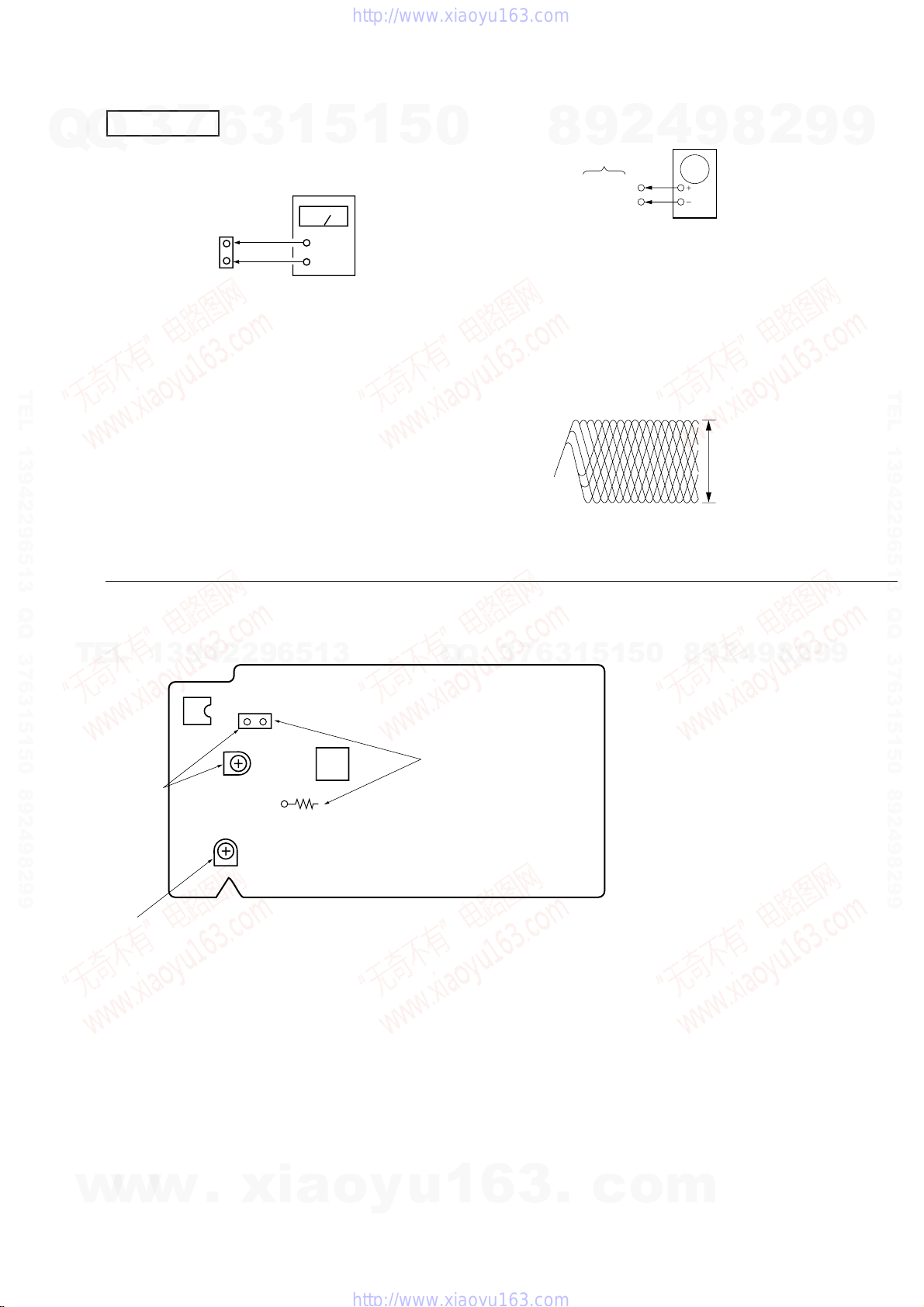
3. Measuring the voltage drop across a resistor by means of a VOM
or battery-operated A C v oltmeter. The “limit” indication is 0.75
V, so analog meters must have an accurate low-voltage scale.
The Simpson 250 and Sanwa SH-63Trd are examples of a passive VOM that is suitable. Nearly all battery operated digital
multimeters that have a 2V AC range are suitable. (See Fig. A)
13942296513
6
To Exposed Metal
Parts on Set
0.15µF
3
1
1.5k
Ω
5
1
AC
voltmeter
(0.75V)
5
0
Q
Q
1. GENERAL
2. DISASSEMBLY
2-1. CD Door ............................................................................... 5
2-2. Back Panel ........................................................................... 5
2-3. CD Mechanism Deck ............................................................ 6
2-4. Front Panel and Main Board ................................................. 6
2-5. CD Tray ............................................................................... 7
2-6. CD Decoder Board................................................................7
2-7. Base Unit ............................................................................. 8
3. MECHANICAL ADJUSTMENTS ................................9
4. ELECTRICAL ADJUSTMENTS ................................. 9
5. DIAGRAMS
5-1. Circuit Boards Location ...................................................... 14
5-2. Brock Diagrams
5-3. IC Brock Diagrams ............................................................. 25
5-4. Printed Wiring Board —Main Section — ........................... 30
5-5. Schematic Diagram — Main Section — ............................ 35
5-6. Schematic Diagram —CD Section — ................................ 39
5-7. Printed Wiring Board —CD Section —.............................. 43
5-8. Printed Wiring Board — Panel Section — ......................... 48
5-9. Schematic Diagram —Panel Section — ............................. 53
7
3
5-10. Schematic Diagram — Tuner Section —.........................58
5-11. Printed Wiring Board — Tuner Section — ...................... 61
5-12. IC Pin Function ................................................................ 65
TABLE OF CONTENTS
4
2
9
8
.......................................................................... 4
• Tuner Section................................................................... 15
• CD Section ....................................................................... 17
• Deck Section .................................................................... 19
• Main Section .................................................................... 21
• Power Section .................................................................. 23
0
5
1
5
1
3
6
9
8
9
2
8
4
2
9
8
9
2
9
9
9
TEL 13942296513 QQ 376315150 892498299
Earth Ground
Fig. A. Using an AC voltmeter to check AC leakage.
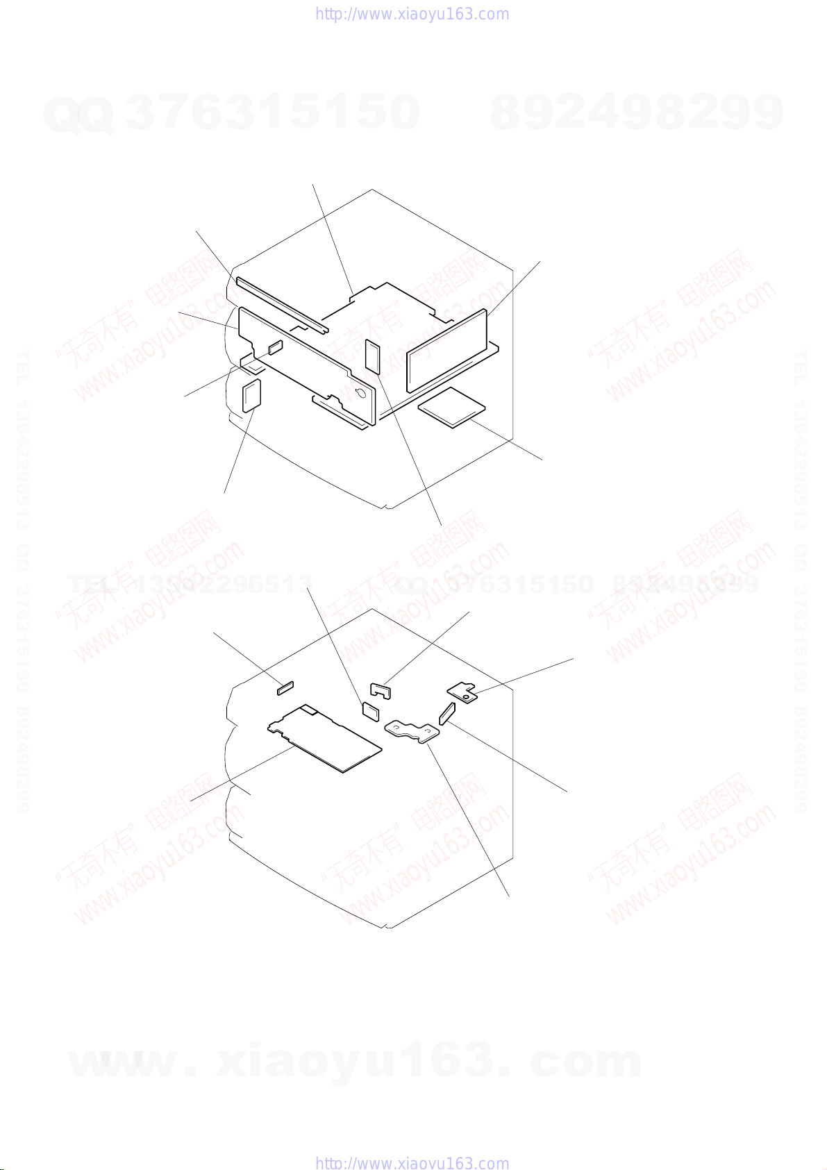
6. EXPLODED VIEWS
6-1. Case and Back Panel Section .............................................. 67
6-2. Front Panel Section ............................................................. 68
6-3. Cassette Mechanism Deck Section 1 .................................. 69
6-4. Cassette Mechanism Deck Section 2 .................................. 70
6-5. CD Mechanism Deck Section 1 .......................................... 71
6-6. CD Mechanism Deck Section 2 .......................................... 72
6-7. Base Unit Section................................................................73
7. ELECTRICAL PARTS LIST ........................................ 74
w
w
w
.
xia
o
y
u
1
6
3
— 3 —
.
c
o
m
SECTION 1
GENERAL
Location of Parts and Controls
7
Q
Q
TEL 13942296513 QQ 376315150 892498299
!¢
TEL
3
!∞ !§ !¶ !•
13942296513
6
1
!ª
3
2
@º @¡
1
5
1
5
0
3
465
@™
@£
!º
@¢
@∞
@¶@§
Q
Q
789!¡!™!£
@•
3
@ª
7
4
2
9
8
1 Disc tray
2 DISC 1 button
3 DISC 2 button
4 DISC 3 button
5 § OPEN/CLOSE button
6 DISC SKIP button
7 VOLUME knob
8 CLOCK SET button
9 TIMER SET, CLOCK LIGHT button
!º TIMER MODE button
!¡ Display window
!™ Remote sensor
!£ POWER button
!¢ PHONES jack
!∞ p (stop) button
¢
!§ P (play/pause) button
!¶ SHUFFLE buttom
!• PROGRAM button
!ª REPEAT button
@º CD button
@¡ TAPE button
@™ PHONO button
@£ TUNER/BAND button
@¢ PRESET – button
@∞ PRESET + button
@§ MEMORY button
@¶ – TUNING +/≠ 0/
) ± buttons
@• DBFB button
@ª PRESET EQ button
#º Deck B
5
1
3
6
#¡ Tape operating buttons
r (recording) (for deck A only)
· (play)
0 (fast rewind)
) (fast forward)
p6 (stop/eject)
P (pause)
#™ Deck A
1
5
0
9
8
9
8
2
4
2
9
8
9
2
9
9
TEL 13942296513 QQ 376315150 892498299
9
#™
w
w
w
.
xia
#¡
#º
o
y
u
1
6
3
— 4 —
.
c
o
m
Q
Note: Follow the disassembly procedure in the numerical order given.
Q
3
2-1. CD DOOR
7
6
3
1
5
1
5
SECTION 2
DISASSEMBLY
0
CD door
8
9
2
4
9
8
2
9
9
TEL 13942296513 QQ 376315150 892498299
1
Pull out the CD tray and remove the
CD door with releasing claws into the
direction of arrow.
TEL
13942296513
2-2. BACK PANEL
7
Back panel
Q
Q
3
7
6
3
1
5
1
5
0
8
9
2
4
9
8
2
9
TEL 13942296513 QQ 376315150 892498299
9
w
w
5
3
w
Two screws
(BVTP3x10)
Two screws
(BVTP3x10)
1
Two screws
(BVTP3x10)
2
.
xia
Three screws
(BVTP3x10)
4
o
Five screws
y
u
1
6
(BVTP3x10)
— 5 —
3
.
6
Five screws
(BVTP3x10)
c
o
m
2-3. CD MECHANISM DECK
7
Q
Q
TEL 13942296513 QQ 376315150 892498299
3
1
Two screws
(BVTP3x10)
6
1
3
4
Flat type wire
(CN09)
5
1
5
5
CD mechanism deck
0
8
9
4
2
3
Harness (CN08)
9
8
2
9
9
TEL 13942296513 QQ 376315150 892498299
2-4. FRONT PANEL AND MAIN BOARD
The TC mechanism deck section can be
TEL
removed with six screws.
13942296513
6
Connector
(CN202)
5
Connector
(CN203)
4
Two screws
(BVTP3x10)
Q
Q
8
Harness
(CN205)
7
Connector
(CN201)
2
Two screws
(BVTP3x10)
6
7
3
3
Screw (BVTP3x10)
3
1
1
5
9
Connector
(CN701)
0
5
!™
Main board
9
8
1
Tuner board
2
4
9
8
2
9
9
!¡
Front panel
w
w
w
.
xia
o
y
u
1
6
3
0
Three screws
(BVTP3X10)
— 6 —
2
Rivet
.
c
o
m
Q
2-5. CD TRAY
Q
3
7
6
3
1
5
1
Screw (BVTP3x10)
2
Bracket
1
5
0
8
9
2
4
9
2
8
3
Screw (BVTP3x10)
9
9
TEL 13942296513 QQ 376315150 892498299
5
CD tray
2-6. CD DECODER BOARD
TEL
13942296513
2
Two screws
(BVTP3x10)
7
CD decoder board
Q
Q
4
Flat type wire (CN06)
3
7
6
3
1
5
5
8
0
5
1
Connector (CN05)
6
Flat type wire
(CN01)
9
4
2
Bracket
9
4
8
2
9
TEL 13942296513 QQ 376315150 892498299
9
w
w
w
.
xia
3
Two claws
o
y
u
1
6
3
— 7 —
1
Two screws (BVTP3x6)
.
c
o
m
2-7. BASE UNIT
Q
Q
3
7
6
3
2
1
UD-cam
5
1
5
1
Screw
(PTPWH2.6x8)
0
8
9
2
4
9
8
2
9
9
TEL 13942296513 QQ 376315150 892498299
TEL
13942296513
Note: When installing, set to
the groove of UD-cam.
Q
Q
3
4
Base unit
7
6
3
1
1
5
3
Two screws
5
0
8
9
2
4
9
8
2
9
TEL 13942296513 QQ 376315150 892498299
9
w
w
w
.
xia
o
y
u
1
6
3
— 8 —
.
c
o
m
SECTION 3
MECHANICAL ADJUSTMENTS
Precaution
Q
TEL 13942296513 QQ 376315150 892498299
1. Clean the following parts with a denatured alcohol-moistened
Q
swab:
2. Demagnetize the record/playback head with a head demagnetizer.
3. Do not use a magnetized screwdriver for the adjustments.
4. After the adjustments, apply suitable locking compound to the
parts adjusted.
5. The adjustments should be performed with the rated power supply voltage unless otherwise noted.
Torque Measurement
FWD
FWD
back tension
FF/REW
7
3
record/playback heads pinch rollers
erase head rubber belts
capstan idlers
Torque
6
Torque meter Meter reading
CQ-102C
CQ-102C
CQ-201B
3
1
5
1
40 to 70 g • cm
(0.56 - 0.97 oz • inch)
(0.01 - 0.07 oz • inch)
55 to 140 g • cm
(0.76 - 1.94 oz • inch)
5
1 to 5 g • cm
0
DECK SECTION 0 dB=0.775V
1. Demagnetize the record/playback head with a head damagnetizer .
2. Do not use a magnetized screwdriver for the adjustments.
3. After the adjustments, apply suitable locking compound to the
parts adjusted.
4. The adjustments should be performed with the rated power supply voltage unless otherwise noted.
5. The adjustments should be performed in the order given in this
service manual. (As a general rule, playback circuit adjustment
should be completed before performing recording circuit
adjustment.)
6. The adjustments should be performed for both L-CH and RCH.
Record/Playback Head Azimuth Adjustment
(Deck A, Deck B)
SECTION 4
ELECTRICAL ADJUSTMENTS
8
Tape
P-4-A100
WS-48B
9
4
2
Signal
10 kHz, –10 dB
3 kHz, 0 dB
9
2
8
Used for
Azimuth Adjustment
Tape Speed Adjustment
9
9
TEL 13942296513 QQ 376315150 892498299
TEL
13942296513
Q
Q
Note: Perform this adjustments for both decks.
Procedure:
1. Mode : Playback
test tape
P-4-A100
3
7
(10kHz, –10dB)
5
1
3
6
1
5
set
0
SPEAKER
terminal (JK501)
2
9
8
4
9
level meter
2
8
+
–
9
9
w
w
w
.
xia
o
y
u
1
6
3
— 9 —
.
c
o
m
2. Turn the adjustment screw and check output peaks. If the peaks
do not match for L-CH and R-CH, turn the adjustment screw so
Q
Q
that outputs match within 2 dB of peak.
L-CH
peak
R-CH
TEL 13942296513 QQ 376315150 892498299
screw
position
3. Mode: Playback
test tape
P-4-A100
(10kHz, –10dB)
peak
TEL
3
output
level
7
within
2dB
set
6
L-CH
peak
SPEKER
terminal (JK501)
(L-CH)
L
R
3
1
R-CH
peak
oscilloscope
13942296513
SPEKER
terminal (JK501)
(R-CH)
Waveform of oscilloscope
5
1
within 2dB
screw
position
5
4. After the adjustments, apply suitable locking compound to the
parts adjusted.
0
Adjustment Location:
Adjustment screws
REC/PB head (deck A)
or PB head (deck B)
Tape Speed Adjustment (Deck A)
Procedure:
1. Mode: Playback
test tape
WS-48B
(3kHz, 0dB)
2. Adjust the SFR201 so that the frequency counter reads 3,000
Q
Adjustment Location:
[MAIN BOARD] — Component side —
+90
Hz ± Hz.
–60
3
Q
7
8
6
3
set
9
1
5
4
2
frequency counter
SPEAKER
terminal (JK501)
0
5
1
9
8
+
–
9
8
2
4
2
9
8
9
2
9
9
TEL 13942296513 QQ 376315150 892498299
9
w
w
in phase
w
good
45˚
90˚
.
xia
135˚ 180˚
wrong
o
y
u
CN301
1
6
CN205
SFR201
Tape Speed
3
.
c
o
m
— 10 —
TUNER SECTION 0 dB=1µV
Q
Q
AM T uning Volta ge Adjustment
Procedure:
1. Set the reception frequency of the unit to 530 kHz.
TEL 13942296513 QQ 376315150 892498299
2. Adjust L105 for 1.2 ± 0.05 V reading on the DC voltmeter.
3. Set the reception frequency of the unit to 1,710 kHz.
4. Confirm that the voltage reading on the DC voltmeter is within
8.0 ± 0.5 V.
Adjustment Location: TUNER board
AM T racking Adjustment
3
7
Tuner board
TP2
(VT)
6
3
1
5
DC voltmeter
+
–
loop antenna
1
5
0
loop antenna
(Supplied accessories)
8
9
2
4
9
8
2
9
9
TEL 13942296513 QQ 376315150 892498299
AM RF SSG
TEL
13942296513
30% amplitude
modulation by
400Hz signal
Procedure:
1. Tune the set to 600 kHz.
2. Set the output of AM RF SSG so that the input level of the set
will become 60 dB (µV/m).
3. Adjust L104 so that when the waveform on the oscilloscope is
maximum, no noise appears.
4. Tune the set to 1,400 kHz.
FM T uning Voltage Adjustment
DC voltmeter
Tuner board
TP2
(VT)
+
–
60cm
Field strength dB (µV/m) = SSG output level dB (µV/m) –26dB.
Q
Q
set
3
terminal (JK101)
5. Adjust TC102 so that when the wa veform on the oscilloscope is
maximum, no noise appears.
• Repeat the procedures in each adjustment several times, and the
tracking adjustment should be finally done by the trimmer
capacitors.
Adjustment Location: TUNER board
AM antenna
5
1
3
6
7
1
5
0
8
9
2
4
9
8
2
9
9
Procedure :
1. Set the reception frequency of the unit to 87.5 MHz.
2. Adjust L103 f or 1.2 ± 0.05V reading on the DC voltmeter.
3. Set the reception frequency of the unit to 108 MHz.
4. Confirm that the voltage reading on the DC voltmeter is within
7.8 ± 0.5V.
w
w
w
Adjustment Location: TUNER board
.
xia
o
y
u
1
— 11 —
6
3
.
c
o
m
FM T racking Adjustment
7
Q
Q
Procedure:
FM RF SSG
FM ANTENNA terminal (JK101)
Carrier frequency : 90 MHz, 106 MHz
Modulation : AUDIO 1kHz, 75kHz deviation (100%)
Output level : 20 dB (at 75
1. Tune the set to 90 MHz.
TEL 13942296513 QQ 376315150 892498299
2. Adjust L102 so that when the waveform on the oscilloscope is
maximum, no noise appears.
3. Tune the set to 106 MHz.
4. Adjust TC101 so that when the wa veform on the oscilloscope is
maximum, no noise appears.
• Repeat the procedures in each adjustment several times, and the
tracking adjustment should be finally done by the trimmer
capacitors.
Adjustment Location: TUNER board
3
set
Ω
6
open)
1
5
3
SPEAKER terminal (JK501)
1
oscilloscope
+
–
5
FM Tuned Level Adjustment
0
Carrier frequency : 98 MHz
Modulation : AUDIO 1 kHz, 75 kHz
Output level : 28 dB (at 75
Procedure:
1. Supply a 28 dB 98 MHz signal from the ANTENNA terminal.
2. Tune the set to 98 MHz.
3. Adjust SFR101 to the point (moment) w hen the TUNED indica-
Adjustment Location: TUNER board
FM RF SSG
tor will change from going off to going on.
9
8
75
deviation (100%)
2
Ω
coaxial
Ω
open)
4
9
FM ANTENNA terminal
(JK101)
8
set
2
9
9
TEL 13942296513 QQ 376315150 892498299
Adjustment Location
[TUNER BOARD] — Component side —
TEL
JK101
L104
TC102
13942296513
FM T uning V oltage
TP2 (VT)
L103
TC101
L102
L105
AM T rac king
AM T uning Voltage
FM T racking
FM T uned Level
SFR101
CN101
Q
Q
3
7
6
3
1
5
1
5
0
8
9
2
4
9
8
2
9
9
w
w
w
.
xia
o
y
u
1
6
3
— 12 —
.
c
o
m
CD SECTION
Q
Q
Focus Bias Adjustment
Procedure:
1. Connect DC voltmeter to test point CN12 (FEO), (VC) on CD
DECODER board.
2. Turned Power switch on.
TEL 13942296513 QQ 376315150 892498299
3. Put disc (YEDS-18) in and stop.
4. Adjust VR01 so that the DC voitmeter reading is 0 ± 20 mV.
Adjustment Location: CD DECODER board
3
7
6
CD DECODER
board
CN12
FEO
VC
3
1
5
DC voltmeter
+
–
1
5
0
RF Level Check
Procedure :
1. Connect oscilloscope to test point TP (RF) on CD DECODER
board.
2. Turned Power switch on.
3. Put disc (YEDS-18) in and playback.
4. Confirm that oscilloscope waveform is clear and check RF signal level is correct or not.
Note: Clear RF signal waveform means that the shape “◊” can be
Adjustment Location: CD DECODER board
CD DECODER
9
8
board
TP (RF)
CN12 (VC)
clearly distinguished at the center of the waveform.
9
level: 1.0 Vp-p
oscilloscope
4
2
2
+0.3
–0.2
9
8
VOLT/DIV: 200 mV
TIME/DIV: 500 nS
9
TEL 13942296513 QQ 376315150 892498299
Adjustment Location
[CD DECODER BOARD] — Component side —
TEL
13942296513
CN12
IC03
Focus Bias
Focus Gain
Focus Gain Adjustment (VR02)
This gain has a margin, so even if it is slightly off.
There is no problem.
Therfore, do not perform this adjusment.
Please note that it should be fixed to mechanical center position
when you moved and do not know original position.
VR01
VC
VR02
FEO
IC01
R07
Q
Q
RF Level
3
7
6
3
1
5
1
5
0
8
9
2
4
9
8
2
9
9
w
w
w
.
xia
o
y
u
1
6
3
— 13 —
.
c
o
m
5-1. CIRCUIT BOARDS LOCATION
7
Q
Q
PANEL board
3
6
3
DISC LED board
1
SECTION 5
DIAGRAMS
5
1
5
0
MAIN Board
8
2
9
TUNER board
4
9
8
2
9
9
TEL 13942296513 QQ 376315150 892498299
SENSOR board
R/P Switch board
O/C board
TEL
13942296513
SW (C) board
SW (D) board
Q
Q
7
3
SW (B) board
AC SUPPLY board
1
3
6
5
1
5
9
8
0
MOTOR board
2
4
9
8
2
9
TEL 13942296513 QQ 376315150 892498299
9
CD DECODER board
w
w
w
.
xia
o
y
u
1
6
3
— 14 —
SW (A) board
MOTOR (6P) (S) board
.
c
o
m
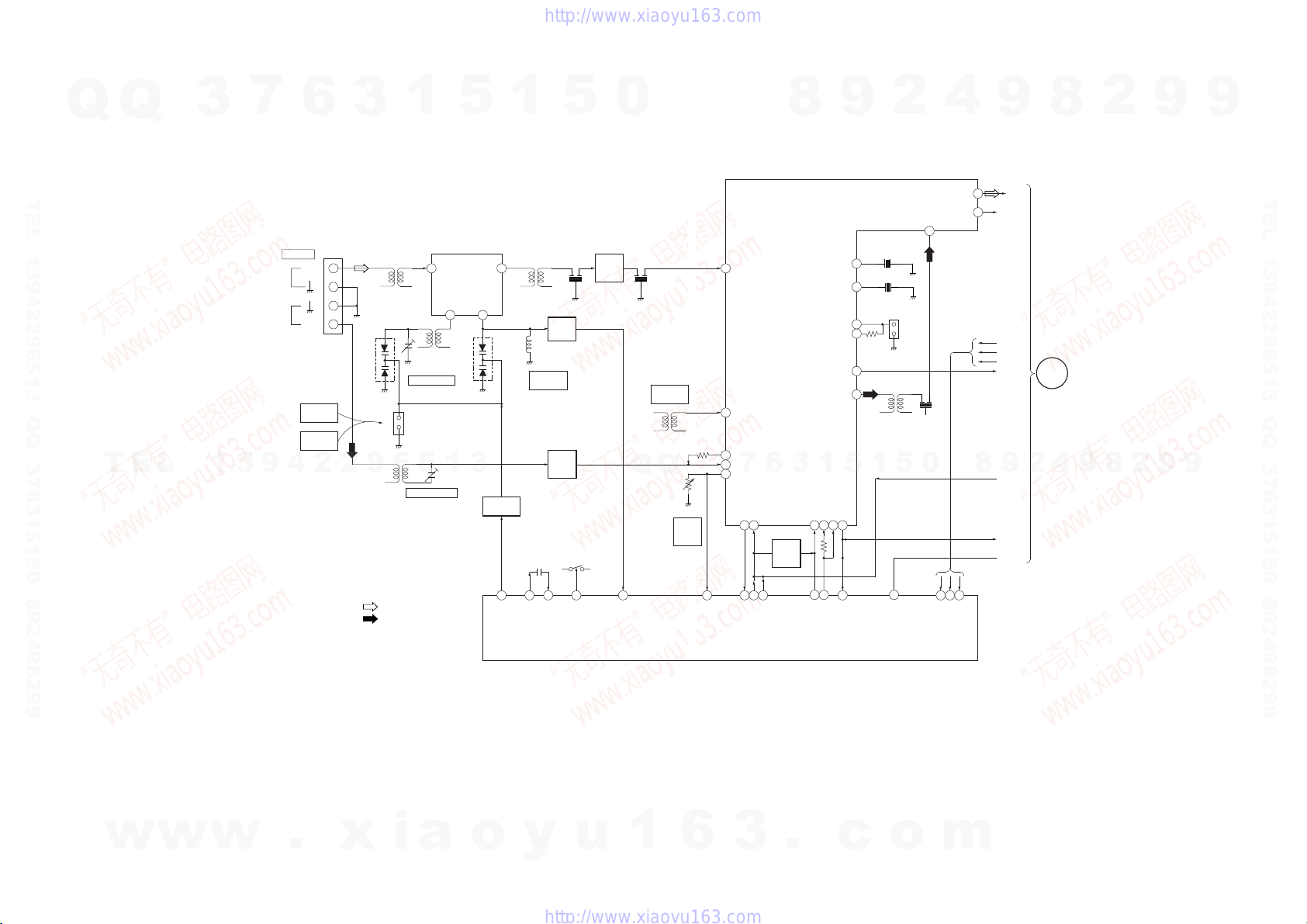
6-2. BLOCK DIAGRAMS
Q
— TUNER SECTION —
Q
3
7
6
3
1
5
1
TEL 13942296513 QQ 376315150 892498299
JK101
T
E
L
1
3
9
ANTENNA
4
FM
75 OHM
AM
TP2
AM TUNING
VOLTAGE
FM TUNING
VOLTAGE
2
D106
2
9
• R CH is omitted
• Signal path
: FM
: AM
L101
G
L104
6
RF IN IF OUT
1 6
MAX IN OSC
TC101,L102
FM TRACKING
TP2VT
5
1
TC102
AM TRACKING
L104,TC102
FM FRONT
END
IC101
3 8
D107
3
L.P.F
Q107,108
21 1 24
PD 1
T101
L103
FM TUNING
VOLTAGE
X201
7.2MHz
X IN
L103
FM OSC
AM RF
B+
X OUT
AMP
Q102
AMP
Q106
5
CF101
10.7MHz
Q105
0
CF102
FM IF
10MHz
AMP
Q101
L105
AM TUNING
VOLTAGE
L105
Q
Q
B+
19
17
FM IN
FM B+
PLL
IC201
SFR101
FM
TUNED
LEVEL
1 FM IF
23
OSC
22
AFC
21
AM RF
7
3
24
OSC/FMSD
6 10
7 15
18
AM IN
TU LED
SD/IN
AM/FM
16
H CTR
6
L CTR
8
3
AGC
CONT.
Q109
FM/AM MPX
IC102
201112 13
12 13
MPX VCO
1
SMET
SD
FM DET
MPX IN
AM/FM
ST IND
AM MIX
PH DET
AM/FM
PH DET
9
8
17
16
18
7
2
5
PL DET
14
ST/MONO
10.4MHz
1
CF104
CF105
19MHz
T102
2
IF
TP1
G
5
5
DO
AM IF
4
0
4
L OUT
R OUT
3 4
2
DI
CE
HCD-G1300
9
2
8
TU L
SECTION
(Page 21)
2
8
A
MAIN
4
9
14
15
R CH
DI
CLK
CE
STIND
9
8
MUTE
STEREO
DO
CLK
2
9
9
9
TEL 13942296513 QQ 376315150 892498299
9
w
w
w
.
09
x
i
— 15 —
a
o
y
u
1
6
3
.
c
o
m
— 16 —
HCD-G1300
— CD SECTION —
Q
Q
3
7
6
3
1
5
1
5
0
8
9
2
4
9
8
2
9
9
OPTICAL PICK-UP BLOCK
DETECTOR
TEL 13942296513 QQ 376315150 892498299
A
C
B
D
E
F
7
B+
LASER DIODE
PD
T
2-AXIS
DEVICE
• R CH is omitted
• Signal path
: CD
E
TRACKING
COIL
FOCUS
COIL
LD
L
4
1
2
5
6
10
APC
Q01
LD ON
Q02
FOCUS
TRACKING
1
3
RF LEVEL
CN12
M102
SLED
MOTOR
M101
SPINDLE
MOTOR
2
1
9
M
M
09
VC
4
FOCUS
TRACKING
VR01
3536PD1
PD2
E
39
F
38
LD
33
PD
34
48
••
45
ATSC
FEO
1
2
FEBIAS
37
VO3(+)
18
VO3(-)
17
VO4(+)
15
VO4(-)
16
VO2(+)
12
VO2(-)
•
11
VO1(+)
13
VO1(-)
•
14
FOCUS/TRACKING
SERVO, RF AMP
IC01 (1/2)
VC
2
TRACKING
COIL DRIVE
FOCUS/TRACKING
COIL DRIVE,
SPINDLE/SLED
MOTOR DRIVE
SLED MOTOR
SPINDLE
COIL
DRIVE
FOCUS
IC03
DRIVE
MOTOR
DRIVE
9
DATA
SENS
C. OUT
XRST
FE M
TA M
CLK
XLT
FOK
FE O
TA O
VIN3
VIN4
VIN2
VIN1
EI
6
31RF 0
CN2
42TEO
VC
1
16
15
24
VR02
SLED SERVO
IC01 (2/2)
SL O
SL M
OP
OUT
FOCUS
GAIN
3
SL P
14
23IN -
9MUTE
40
19
20
21
24
23
25
22
6
7
13
12
5
25
27
6
4
36
17
16
15
13
14
23
22
8
RF
CLKO
XLTO
DATO
SEIN
CNIN
FOK
XLON
XRST
Q
DIGITAL SIGNAL PROCESSOR, D/A CONVERTER, DIGITAL FILTER
DIGITAL
PLL
DEMODULATOR
SUB CODE
PROCESSOR
SERVO
AUTO
SEQUENCER
Q
MDP
25
M103
TURN
TABLE
MOTOR
M104
TRAY
MOTOR
CPU
INTERFACE
3
M
M
EFM
7
TURN TABLE
MOTOR DRIVE
Q10,11,14,15
TURN TABLE
MOTOR DRIVE
TRAY MOTOR
IC04
DIGITAL
CLV
6
CONTROL
Q13
DRIVER
Q06 - Q09
INTERFACE
D/A
3
S05
LIMIT
SWITCH
CLOCK
GENERATOR
1
SPOA
18
6
7
11
8
9
4
74 73
33.8688MHz
T.T+
T.T-
DOWN
TRAY +
TRAY -
XRST
XTA0
5
XLT01
DIGITAL
FILTER
+
1BIT
DAC
XTA1
1
MUTE
6
2
NLPWM
LPWM
RPWM
NRPWM
DATA
SQCK
CLOK
SQSO
SCOR
SENS
XLAT
5
B.BOOST
MUTE
DATA I
CLOK
CONTROL
TRAY/TABLE
MOTOR
DRIVER,
REG CONTROL
IC02
MIX AMP
R CH
IC05
+
-
CD L
DATA
SQCK
SQSO
SCOR
SENS
TEL 13942296513 QQ 376315150 892498299
70
69
78
77
9
5
11
4
1
7
C
10
4
2
9
UP DOWN
8
S01
OPTICAL PICK-UP
UP/DOWN DET
0
5
13
14
15
STB
3
10
UP
XLAT
COUNT
FOK
DI
CLK
STB
B. BOOST
9
UP
DOWN
CONTROL
MUTE
MAIN
SECTION
(Page 21)
8
2
E
9
POWER
SECTION
(Page 23)
9
w
w
w
.
— 17 —
x
i
a
o
y
u
1
6
3
.
c
o
— 18 —
m
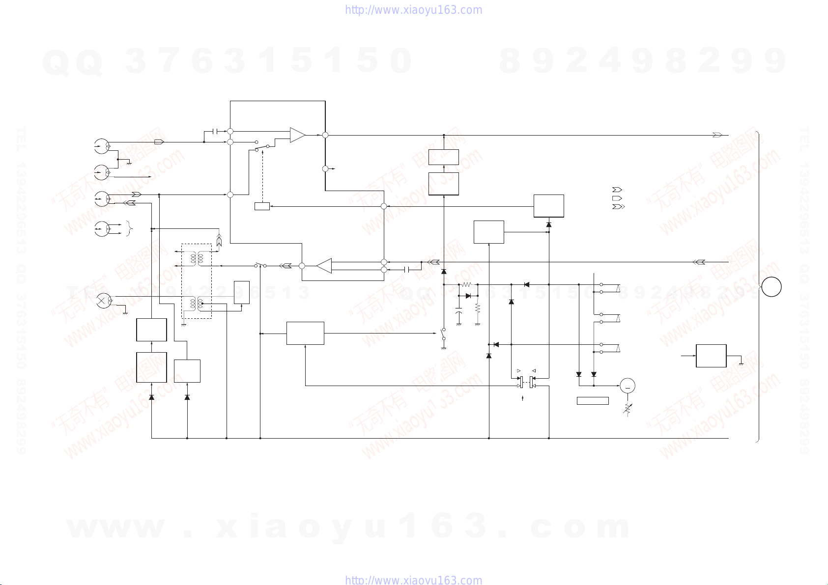
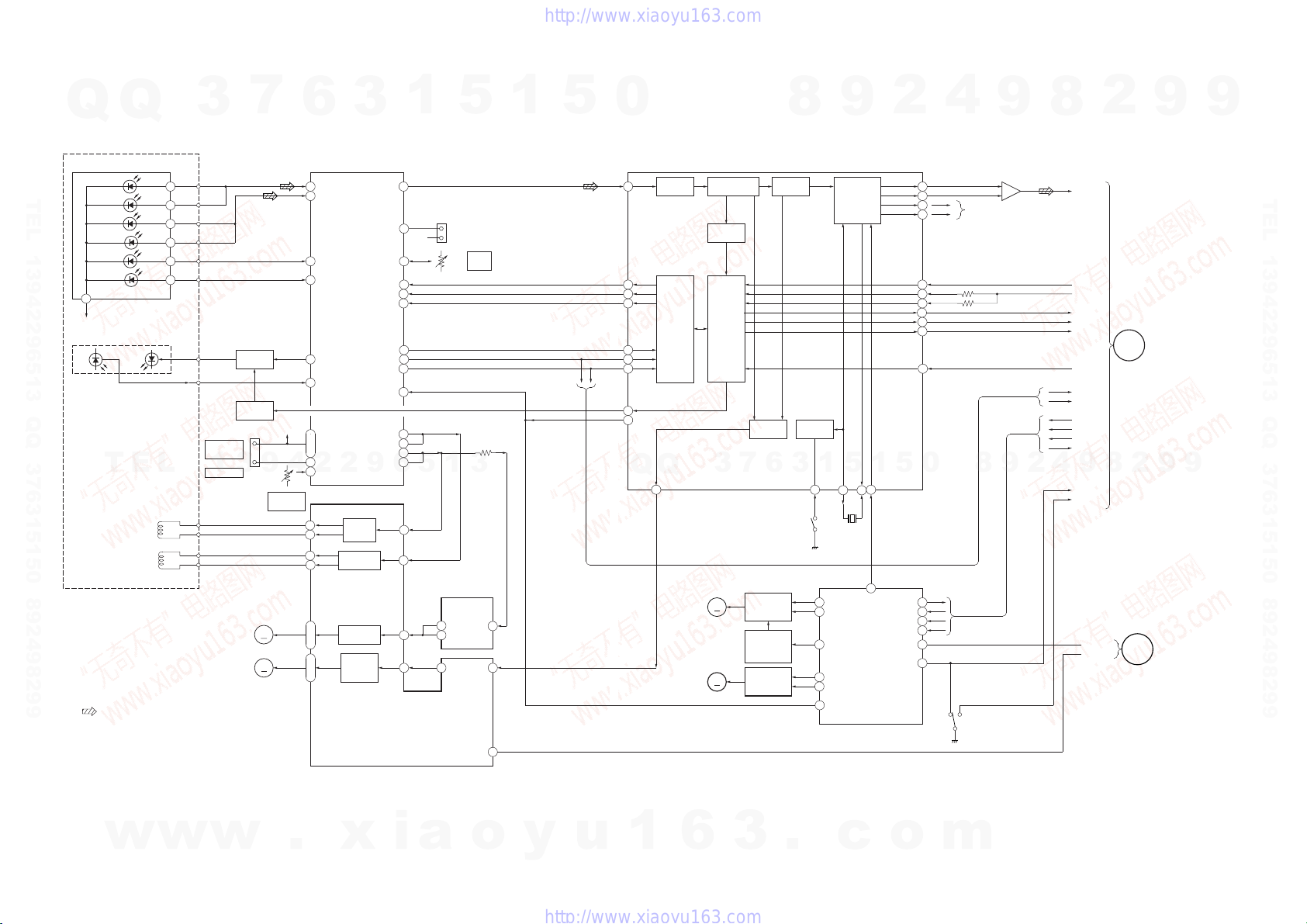
— DECK SECTION —
HCD-G1300
Q
Q
3
7
6
3
TEL 13942296513 QQ 376315150 892498299
TAPE B
HP901
PB HEAD
R CH
TAPE A
HRP901
REC/PB
T
HEAD
HE901
E
ERASE
HEAD
L
R CH
1
3
PLAY/REC
CONTROL
Q203,205
PLAY/REC
CONTROL
DRIVE
Q207
D208
R CH
R CH
9
BIAS OSC COIL
4
PLAY/REC
CONTROL
Q201
L201
D209
2
2
1
2
3
CH1/B
9
NF
CH1/A
BIAS
OSD
Q218
Q211
6
1
A/B
5
1
5
-
+
REC/PLAY
EQ AMP
IC201
9
3
REC SWITCH
DRIVE
Q217
PRE
OUT
PREOUT
REC
OUT
1
5
R CH
20
+
-
5
TAPE A/TAPE B
REC IN
0
8
9
2
4
9
8
2
9
9
TEL 13942296513 QQ 376315150 892498299
PB L
MUTE
Q209
B +
0
D207D206
SFR201
TAPE SPEED
• R CH is omitted
• Signal path
: PB (DECK A)
: PB (DECK B)
: REC (DECK A)
S201
A DECK
2
9
8
S202
B DECK
S203
PLAY
M
M901
REEL/CAPSTAN
MOTOR
4
REC L
B
9
9
2
8
9
GROUND
B +
SWITCH
Q220
MAIN
SECTION
(Page 21)
MUTE
SWITCH
Q216
TAPE A/B
D203
1
D213
SW201
REC/PLAY
SWITCH
PLAY
REC
5
SWITCH
Q213
D201
1
5
19
TAPE A
SWITCH
Q214
11
NF
10
Q
Q
D205
Q219
3
D202
+
7
6
3
D212
D211
w
09
w
w
.
x
i
— 19 —
a
o
y
u
1
6
3
.
c
o
CD SYNC
m
— 20 —
 Loading...