

Page 1
HCD-G101
SERVICE MANUAL
HCD-G101 is the tuner, deck, CD
and amplifier section in MHC-G101.
Model Name Using Similar Mechanism NEW
CD
SECTION
TAPE
DECK
SECTION
CD Mechanism Type CX3
Base Unit Type KSM-213BCM
Optical Pick-up Type KSS-213B/S-N
Model Name Using Similar Mechanism HCD-H100
Tape Transport
Mechanism Type
US Model
Canadian Model
DECK-A
DECK-B
TK20FX-SW943-800
TK20FX-SW943-800
SPECIFICATIONS
COMPACT DISC DECK RECEIVER
MICROFILM
— 1 —
Page 2
SERVICING NOTE
CAUTION
Use of controls or adjustments or performance of procedures
other than those specified herein may result in hazardous radiation exposure.
Notes on chip component replacement
• Never reuse a disconnected chip component.
• Notice that the minus side of a tantalum capacitor may be
damaged by heat.
Flexible Circuit Board Repairing
• Keep the temperature of soldering iron around 270˚C
during repairing.
• Do not touch the soldering iron on the same conductor of the
circuit board (within 3 times).
• Be careful not to apply force on the conductor when soldering
or unsoldering.
Laser component in this product is capable of emitting radiation
exceeding the limit for Class 1.
This appliance is classified as
a CLASS 1 LASER product.
The CLASS 1 LASER PRODUCT MARKING is located on
the rear exterior.
NOTES ON HANDLING THE OPTICAL PICK-UP BLOCK
OR BASE UNIT
The laser diode in the optical pick-up block may suffer electrostatic
break-down because of the potential difference generated by the
charged electrostatic load, etc. on clothing and the human body.
During repair, pay attention to electrostatic break-down and also
use the procedure in the printed matter which is included in the
repair parts.
The flexible board is easily damaged and should be handled with
care.
NOTES ON LASER DIODE EMISSION CHECK
The laser beam on this model is concentrated so as to be focused on
the disc reflective surface by the objective lens in the optical pickup block. Therefore, when checking the laser diode emission, observe from more than 30 cm away from the objective lens.
This caution
label is located
inside the unit.
SAFETY-RELATED COMPONENT WARNING !!
COMPONENTS IDENTIFIED BY MARK ! OR DO TTED LINE
WITH MARK ! ON THE SCHEMATIC DIAGRAMS AND IN
THE PARTS LIST ARE CRITICAL TO SAFE OPERATION.
REPLACE THESE COMPONENTS WITH SONY PARTS
WHOSE PART NUMBERS APPEAR AS SHOWN IN THIS
MANUAL OR IN SUPPLEMENTS PUBLISHED BY SONY.
ATTENTION AU COMPOSANT AYANT RAPPORT
À LA SÉCURITÉ!!
LES COMPOSANTS IDENTIFIÉS P AR UNE MARQUE ! SUR
LES DIAGRAMMES SCHÉMATIQUES ET LA LISTE DES
PIÈCES SONT CRITIQUES POUR LA SÉCURITÉ DE
FONCTIONNEMENT. NE REMPLA CER CES COMPOSANTS
QUE PAR DES PIÈCES SONY DONT LES NUMÉROS
SONT DONNÉS DANS CE MANUEL OU DANS LES
SUPPLÉMENTS PUBLIÉS PAR SONY.
— 2 —
Page 3
SAFETY CHECK-OUT
TABLE OF CONTENTS
After correcting the original service problem, perform the following safety checks before releasing the set to the customer:
Check the antenna terminals, metal trim, “metallized” knobs, screws,
and all other exposed metal parts for A C leakage. Check leakage as
described below.
LEAKAGE
The AC leakage from any exposed metal part to earth Ground and
from all exposed metal parts to any exposed metal part having a
return to chassis, must not exceed 0.5 mA (500 microampers). Leakage current can be measured by any one of three methods.
1. A commercial leakage tester, such as the Simpson 229 or RCA
WT-540A. Follow the manufacturers’ instructions to use these
instruments.
2. A ba ttery-operated AC milliammeter. The Data Precision 245
digital multimeter is suitable for this job.
3. Measuring the voltage drop across a resistor by means of a VOM
or battery-operated A C v oltmeter. The “limit” indication is 0.75
V, so analog meters must have an accurate low-voltage scale.
The Simpson 250 and Sanwa SH-63Trd are examples of a passive VOM that is suitable. Nearly all battery operated digital
multimeters that have a 2V AC range are suitable. (See Fig. A)
To Exposed Metal
Parts on Set
0.15µF
1.5k
Ω
AC
voltmeter
(0.75V)
1. GENERAL
.......................................................................... 4
2. DISASSEMBLY
2-1. CD Door ............................................................................... 5
2-2. CD Mechanism Deck ............................................................ 5
2-3. Front Panel and Main Board ................................................. 6
2-4. Main Board and H/P Board................................................... 6
2-5. CD Tray ............................................................................... 7
2-6. CD Decoder Board................................................................ 7
2-7. Base Unit ............................................................................. 8
3. MECHANICAL ADJUSTMENTS ................................9
4. ELECTRICAL ADJUSTMENTS ................................. 9
5. DIAGRAMS
5-1. Circuit Boards Location ...................................................... 14
5-2. Brock Diagrams
• Tuner Section................................................................... 15
• CD Section ....................................................................... 17
• Deck Section .................................................................... 19
• Main Section .................................................................... 21
• Power Section .................................................................. 23
5-3. IC Brock Diagrams ............................................................. 25
5-4. Printed Wiring Board —Main Section — ........................... 30
5-5. Schematic Diagram — Main Section — ............................ 35
5-6. Schematic Diagram —Panel Section — ............................. 39
5-7. Printed Wiring Board —Panel Section — .......................... 43
5-8. Printed Wiring Board — CD Section —............................. 47
5-9. Schematic Diagram —CD Section — ................................ 51
5-10. IC Pin Function ................................................................ 54
Earth Ground
Fig. A. Using an AC voltmeter to check AC leakage.
6. EXPLODED VIEWS
6-1. Top and Bottom Cabinet Section ........................................ 56
6-2. Front Panel Section ............................................................. 57
6-3. Cassette Mechanism Deck Section 1 .................................. 58
6-4. Cassette Mechanism Deck Section 2 .................................. 59
6-5. CD Mechanism Deck Section 1 .......................................... 60
6-6. CD Mechanism Deck Section 2 .......................................... 61
6-7. Base Unit Section (KSM-213BCM) ................................... 62
7. ELECTRICAL PARTS LIST ........................................ 63
— 3 —
Page 4
Location of Parts and Controls
SECTION 1
GENERAL
!¢
!∞ !§
1
!™
!£ !¡
!¶
!•
!ª
@º
!º
@¡
3
42
5
6
987
@™ @•@§
@¢@£
@∞
1 Disc tray
2 DISC 1 button
3 DISC 2 button
4 DISC 3 button
5 DISC SKIP button
6 § OPEN/CLOSE button
7 DBFB button
8 VOLUME knob
9 Display window
!º TIMER SET, CLOCK LIGHT button
!¡ TIMER MODE button
!™ Remote sensor
!£ CLOCK SET button
!¢ POWER button
!∞ PHONES jack
¢
!§ P (play/pause) button
!¶ SHUFFLE button
!• PROGRAM button
!ª REPEAT button
@¶
#º#¡
@º p(stop) button
@¡ CD button
@™ TAPE button
@£ TUNER/BAND button
@¢ PRESET – button
@∞ PRESET + button
@§ MEMORY button
@¶ – TUNING +/≠ 0/
) ± buttons
@• PRESET EQ button
@ª Deck B
#º Tape operating buttons
r (recording) (for deck A only)
· (play)
0 (fast rewind)
) (fast forward)
p6 (stop/eject)
P (pause)
#¡ Deck A
@ª
— 4 —
Page 5
SECTION 2
DISASSEMBLY
Note: Follow the disassembly procedure in the numerical order given.
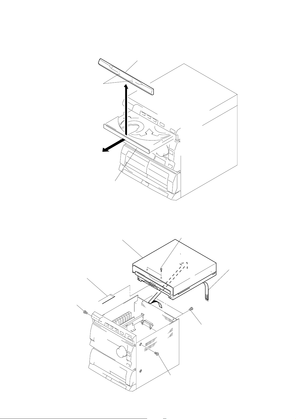
2-1. CD DOOR
CD door
craws
1
Pull out the CD tray and remove the
CD door with releasing claws into the
direction of arrow.
2-2. CD MECHANISM DECK
7
5
Flat type wire (21 core)
(CN09)
3
Screw
(BVTP3x10)
CD mechanism deck
1
Two screws (B3x8)
4
Two screws
(BVTP3x10)
6
Harness
(Main board: CN302)
— 5 —
2
Screw
(BVTP3x10)
Page 6
2-3. FRONT PANEL AND MAIN BOARD
2
Connector
(CN401)
9
Front panel and
Main board
8
Screw
(BVTP3x10)
6
Screw
(BVTP3x10)
3
Screw (BVTP3x8)
HOW TO SET THE
POWER CORD
5
Two screws
(BVTP3x10)
7
Screw
(BVTP3x10)
4
Two screws
(BVTP3x10)
2-4. MAIN BOARD AND H/P BOARD
1
Harness
(CN204)
6
Screw (BVTT3x6)
8
Screw (PTPWH3x10)
0
H/P board
7
Screw
(BVTT3x6)
2
Connector
(CN203)
1
Three screws
(BVTP3x10)
3
Connector
(CN206)
4
Connector
(CN201)
POWER CORD
9
Main board
5
Screw
(BVTP3x8)
— 6 —
Page 7
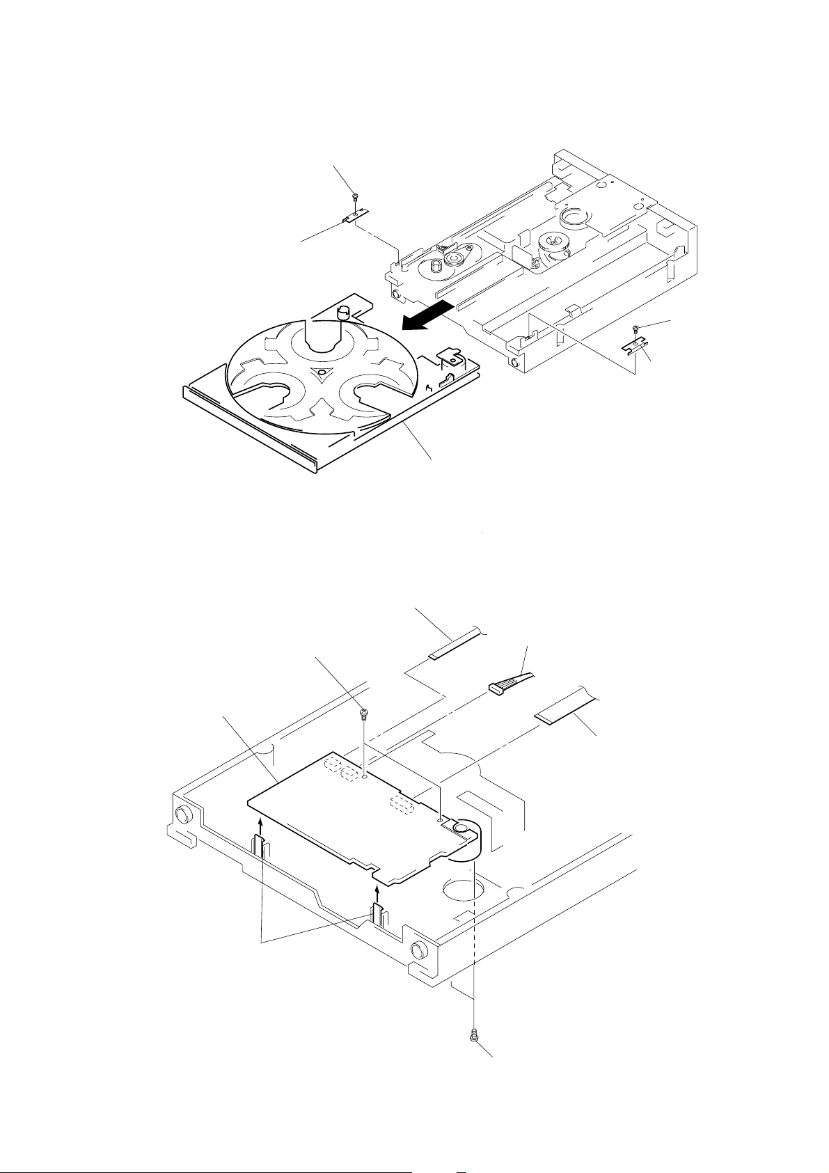
2-5. CD TRAY
1
Screw (BVTP3x10)
2
Bracket
5
CD tray
3
Screw (BVTP3x10)
4
Bracket
2-6. CD DECODER BOARD
7
CD decoder board
2
Two screws
(BVTP3x10)
4
Flat type wire (CN06)
5
Connector (CN05)
6
Flat type wire
(CN01)
3
Two claws
— 7 —
1
Two screws (BVTP3x6)
Page 8
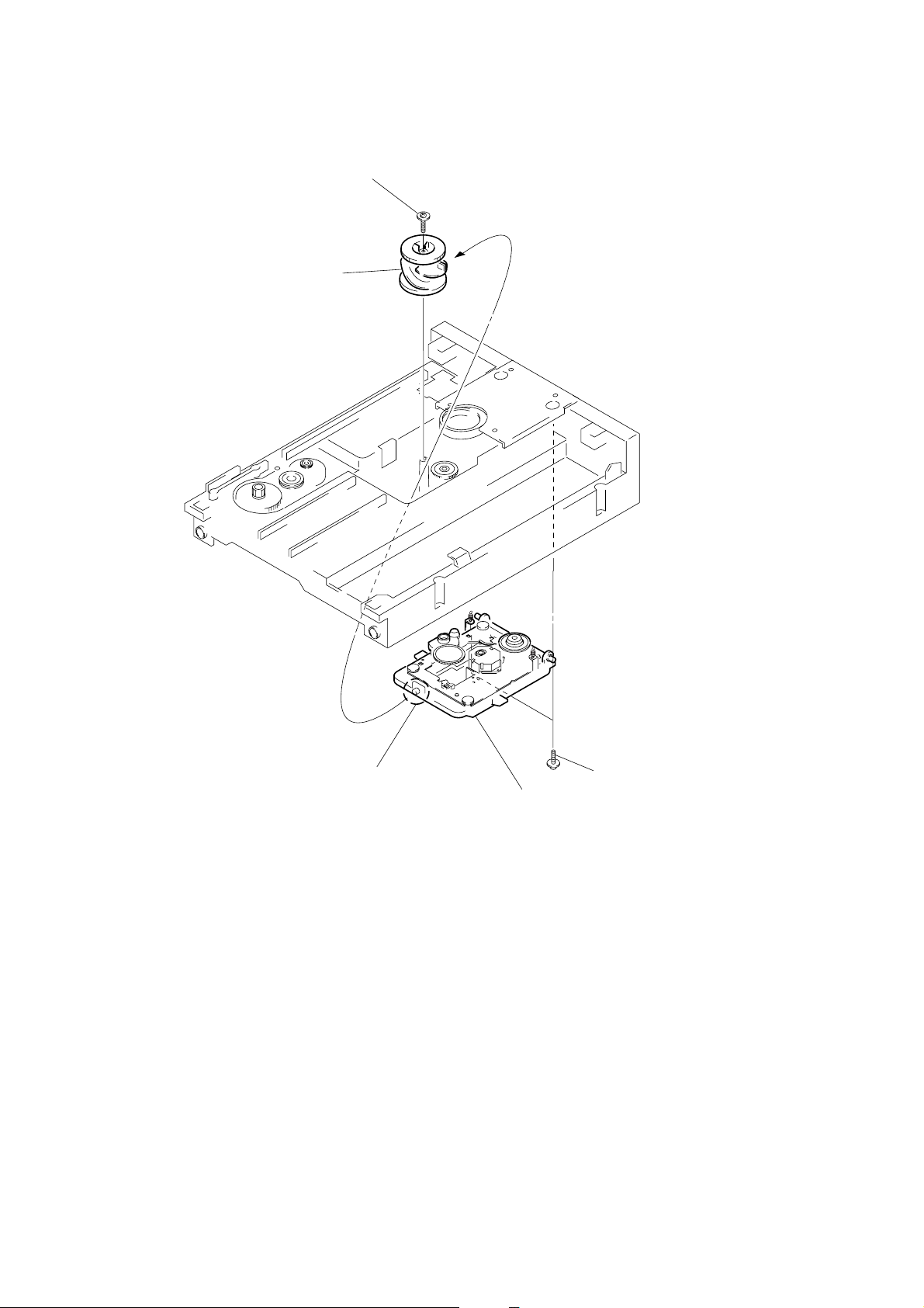
2-7. BASE UNIT
2
1
UD-cam
Screw
(PTPWH2.6x8)
Note: When installing, set to
the groove of UD-cam.
4
Base unit
3
Two screws
— 8 —
Page 9

SECTION 3
MECHANICAL ADJUSTMENTS
SECTION 4
ELECTRICAL ADJUSTMENTS
Precaution
1. Clean the following parts with a denatured alcohol-moistened
swab:
record/playback heads pinch rollers
erase head rubber belts
capstan idlers
2. Demagnetize the record/playback head with a head demagnetizer.
3. Do not use a magnetized screwdriver for the adjustments.
4. After the adjustments, apply suitable locking compound to the
parts adjusted.
5. The adjustments should be performed with the rated power supply voltage unless otherwise noted.
Torque Measurement
Torque
FWD
FWD
back tension
FF/REW
Torque meter Meter reading
CQ-102C
CQ-102C
CQ-201B
40 to 70 g • cm
(0.56 - 0.97 oz • inch)
1 to 5 g • cm
(0.01 - 0.07 oz • inch)
55 to 140 g • cm
(0.76 - 1.94 oz • inch)
DECK SECTION 0 dB=0.775V
1. Demagnetize the record/playback head with a head damagnetizer .
2. Do not use a magnetized screwdriver for the adjustments.
3. After the adjustments, apply suitable locking compound to the
parts adjusted.
4. The adjustments should be performed with the rated power supply voltage unless otherwise noted.
5. The adjustments should be performed in the order given in this
service manual. (As a general rule, playback circuit adjustment
should be completed before performing recording circuit
adjustment.)
6. The adjustments should be performed for both L-CH and RCH.
Tape
P-4-A100
WS-48B
Record/Playback Head Azimuth Adjustment
(Deck A, Deck B)
Note: Perform this adjustments for both decks.
Procedure:
1. Mode : Playback
test tape
P-4-A100
(10kHz, –10dB)
Signal
10 kHz, –10 dB
3 kHz, 0 dB
SPEAKER
terminal (JK302)
Used for
Azimuth Adjustment
Tape Speed Adjustment
level meter
set
+
–
— 9 —
Page 10

2. Turn the adjustment screw and check output peaks. If the peaks
do not match for L-CH and R-CH, turn the adjustment screw so
that outputs match within 2 dB of peak.
L-CH
peak
screw
position
R-CH
peak
output
level
within
2dB
L-CH
peak
R-CH
peak
within 2dB
screw
position
3. Mode: Playback
test tape
P-4-A100
(10kHz, –10dB)
SPEKER
terminal (JK302)
(L-CH)
L
set
R
SPEKER
terminal (JK302)
(R-CH)
Waveform of oscilloscope
oscilloscope
4. After the adjustments, apply suitable locking compound to the
parts adjusted.
Adjustment Location:
Adjustment screws
REC/PB head (deck A)
or PB head (deck B)
Tape Speed Adjustment (Deck A)
Procedure:
1. Mode: Playback
test tape
WS-48B
(3kHz, 0dB)
set
SPEAKER
terminal (JK302)
frequency counter
+
–
2. Adjust the SFR201 so that the frequency counter reads 3,000 Hz
± 90Hz.
Adjustment Location: MAIN board
Sample Value of Wow and flutter
W. RMS (JIS) within 0.3%
(test tape: WS-48B)
in phase
good
45˚
90˚
135˚ 180˚
wrong
[MAIN BOARD] — Component side —
Tape Speed
SFR201
CN204
— 10 —
Page 11

TUNER SECTION 0 dB=1µV
AM T uning Volta ge Adjustment
Main board
TP1
IF
G
VT
DC voltmeter
+
–
Procedure:
1. Set the reception frequency of the unit to 530 kHz.
2. Adjust L105 for 1.2 ± 0.05 V reading on the DC voltmeter.
3. Set the reception frequency of the unit to 1,710 kHz.
4. Confirm that the voltage reading on the DC voltmeter is within
8.0 ± 0.5 V.
Adjustment Location: MAIN board
AM T racking Adjustment
loop antenna
AM RF SSG
Center of
Bar antenna (L104)
set
30% amplitude
modulation by
400Hz signal
Field strength dB (µV/m) = SSG output level dB (µV/m) –26dB.
Procedure:
1. Tune the set to 600 kHz.
2. Set the output of AM RF SSG so that the input level of the set
will become 60 dB (µV/m).
3. Adjust L104 so that when the waveform on the oscilloscope is
maximum, no noise appears.
4. Tune the set to 1,400 kHz.
FM T uning Voltage Adjustment
Main board
TP1
IF
G
VT
DC voltmeter
+
–
Procedure :
1. Set the reception frequency of the unit to 87.5 MHz.
2. Adjust L103 f or 1.2 ± 0.05V reading on the DC voltmeter.
3. Set the reception frequency of the unit to 108 MHz.
4. Confirm that the voltage reading on the DC voltmeter is within
7.8 ± 0.5V.
60cm
5. Adjust TC102 so that when the waveform on the oscilloscope is
maximum, no noise appears.
• Repeat the procedures in each adjustment several times, and the
tracking adjustment should be finally done by the trimmer
capacitors.
Adjustment Location: MAIN board
Adjustment Location: MAIN board
— 11 —
Page 12

FM T racking Adjustment
FM Tuned Level Adjustment
Procedure:
FM RF SSG
set
FM ANTENNA terminal (JK101)
Carrier frequency : 90 MHz, 106 MHz
Modulation : AUDIO 1kHz, 75kHz deviation (100%)
Output level : 20 dB (at 75
SPEAKER terminal (JK302)
Ω
open)
oscilloscope
+
–
1. Tune the set to 90 MHz.
2. Adjust L102 so that when the waveform on the oscilloscope is
maximum, no noise appears.
3. Tune the set to 106 MHz.
4. Adjust TC101 so that when the waveform on the oscilloscope is
maximum, no noise appears.
• Repeat the procedures in each adjustment several times, and the
tracking adjustment should be finally done by the trimmer
capacitors.
Adjustment Location: MAIN board
FM RF SSG
75
Ω
coaxial
set
Carrier frequency : 98 MHz
Modulation : AUDIO 1 kHz, 75 kHz
Output level : 28 dB (at 75
deviation (100%)
Ω
open)
FM ANTENNA terminal
(JK101)
Procedure:
1. Supply a 28 dB 98 MHz signal from the ANTENNA terminal.
2. Tune the set to 98 MHz.
3. Adjust SFR101 to the point (moment) when the TUNED indicator will change from going off to going on.
Adjustment Location: MAIN board
Adjustment Location
[MAIN BOARD] — Component side —
FM T uned Level
SFR101
IC103
TP1
FM T uning Voltage
AM T uning V oltage
L105
IC102
TC102
L104
JK302
FM T racking
L102
L103
TC101
JK101
VT
GND
— 12 —
IF
AM T racking
Page 13

CD SECTION
Note:
1. CD Block is basically constructed to operate without adjustment.
Therefore, check each item in order given.
2. Use YEDS-18 disc (3-702-101-01) unless otherwise indicated.
3. Use an oscilloscope with more than 10MΩ impedance.
4. Clean the object lens by an applicator with neutral detergent
when the signal level is low than specified value with the following checks.
5. Adjust the focus bias adjustment when optical block is replaced.
Focus Bias Adjustment
DC voltmeter
CD DECODER
board
CN12
FEO
VC
Procedure:
1. Connect DC voltmeter to test point CN12 (FEO), (VC) on CD
DECODER board.
2. Turned Power switch on.
3. Put disc (YEDS-18) in and stop.
4. Adjust VR01 so that the DC voitmeter reading is 0 ± 20 mV.
+
–
RF Level Check
CD DECODER
board
TP (RF)
CN12 (VC)
oscilloscope
Procedure :
1. Connect oscilloscope to test point TP (RF) on CD DECODER
board.
2. Turned Power switch on.
3. Put disc (YEDS-18) in and playback.
4. Confirm that oscilloscope waveform is clear and check RF signal level is correct or not.
Note: Clear RF signal waveform means that the shape “◊” can be
clearly distinguished at the center of the waveform.
VOLT/DIV: 200 mV
TIME/DIV: 500 nS
level: 1.0 Vp-p
+0.3
–0.2
Adjustment Location: CD DECODER board
Adjustment Location: CD DECODER board
Focus Gain Adjustment (VR02)
This gain has a margin, so even if it is slightly off.
There is no problem.
Therfore, do not perform this adjusment.
Please note that it should be fixed to mechanical center position
when you moved and do not know original position.
Adjustment Location
[CD DECODER BOARD] — Component side —
CN12
IC03
Focus Bias
VR01
VC
FEO
IC01
R07
RF Level
Focus Gain
VR02
— 13 —
Page 14

5-1. CIRCUIT BOARDS LOCATION
DISC board
SENSOR board
H/P board
SECTION 5
DIAGRAMS
MAIN Board
SW (C) board
POWER TRANSFORMER board
PANEL board
MOTOR (6P) (S) board
SW (B) board
SW (D) board
MOTOR board
SW (A) board
R/P SW board
CD DECODER board
— 14 —
Page 15

5-2. BLOCK DIAGRAMS
— TUNER SECTION —
FM ANTENNA
L104
MW
BAR ANTENNA
JK101
FM
75 OHM
D104
TC102
L101
TC101 L102
D101
TP1
VT
(1/2)
G
TC102, L104
AM TRACKING
• R CH is omitted
• Signal path
: FM
: AM
RF IN IF
1 6
FRONT
MIX IN OSC
3 8
D103
TC101,L102
FM TRACKING
TP1 (1/2)
AM TUNING
VOLTAGE
FM TUNING
VOLTAGE
IC101
END
L.P.F
Q105,106
21 1 24
PD 1
T101
L103
FM TUNING
VOLTAGE
X101
7.2MHz
X IN
L103
FM OSC
AMP
Q102
B+
X OUT
CF101
10.7MHz
Q103
17
FM B+
HCD-G101
L OUT
AM IF
4
R OUT
14
15
R CH
REC MUTE
3 4
2
DI
CE
CLK
FM/AM MPX
IC102
CF104
PH DET
14
PL DET
FM ST
10.7MHz
8
17
CF105
19kHz
T102
IF
TP1
G
(2/2)
CF103
TUNED
SWITCH
Q107
5
DO
16
18
7
2
CF102
FM IF
10.7MHz
AMP
Q101
L105
AM TUNING
VOLTAGE
L105
B+
19
FM IN
PLL
IC103
SFR101
FM
TUNED
LEVEL
1 FM IF
23
OSC
22
AFC
21
AM RF
24
OSC/FMSD
AM/FM
TU LED
6 10
7 15
18
AM IN
SD/IN
16
H CTR
L CTR
FM DET
MPX VCO
MPX IN
AF DET
ST IND
AM MIX
PH DET
SMET
201112 13
12 13
AM/FM
SD SPEED
Q108,109
TU L
REC OUT
DI
CLK
CE
ST/IN
TU MUTE
TUNED
DO 1
A
MAIN
SECTION
(Page 21)
09
— 15 —
— 16 —
Page 16

HCD-G101
— CD SECTION —
OPTICAL PICK-UP BLOCK
DETECTOR
A
C
B
D
E
F
7
B+
LASER DIODE
PD
TRACKING
2-AXIS
DEVICE
• R CH is omitted
• Signal path
: CD
COIL
FOCUS
COIL
DIGITAL SIGNAL PROCESSOR, D/A CONVERTER, DIGITAL FILTER
RF
4
1
2
5
6
10
LD
FOCUS
TRACKING
RF LEVEL
MOTOR
SPINDLE
MOTOR
M102
SLED
M101
APC
Q01
LD ON
Q02
CN12
M
M
2
1
09
VC
FOCUS
TRACKING
VR01
3536PD1
PD2
E
39
F
38
LD
33
PD
34
48
VC
••
45
ATSC
FEO
1
FEBIAS
37
VO3(+)
18
VO3(-)
17
VO4(+)
15
VO4(-)
16
VO2(+)
12
VO2(-)
•
11
VO1(+)
13
VO1(-)
•
14
FOCUS/TRACKING
SERVO, RF AMP
IC01 (1/2)
TRACKING
COIL
DRIVE
FOCUS
COIL DRIVE
FOCUS/TRACKING
COIL DRIVE,
SPINDLE/SLED
MOTOR DRIVE
IC03
SLED MOTOR
DRIVE
SPINDLE
MOTOR
DRIVE
DATA
SENS
C. OUT
XRST
FE M
TA M
CLK
FOK
FE O
TA O
XLT
VIN3
VIN4
VIN2
VIN1
31RF 0
CN2
42TEO
VC
16
15
24
VR02
SLED SERVO
IC01 (2/2)
SL O
SL M
OP
OUT
FOCUS
GAIN
SL P
14
23IN -
9MUTE
EI
40
19
20
21
24
23
25
22
6
7
13
12
25
27
6
4
DIGITAL
36
PLL
DEMODULATOR
SUB CODE
PROCESSOR
CLKO
17
XLTO
16
DATO
15
SERVO
AUTO
SEQUENCER
SEIN
13
CNIN
14
FOK
23
XLON
22
8
XRST
MDP
25
M103
TURN
TABLE
MOTOR
M104
TRAY
MOTOR
CPU
INTERFACE
M
M
EFM
IC04
DIGITAL
CLV
TURN TABLE
MOTOR DRIVE
Q10,11,14,15
TURN TABLE
MOTOR DRIVE
CONTROL
Q13
TRAY MOTOR
DRIVER
Q06 - Q09
D/A
INTERFACE
S05
LIMIT
SWITCH
CLOCK
GENERATOR
SPOA
18
6
7
11
8
9
4
XTA0
74 73
33.8688MHz
T.T+
T.T-
DOWN
TRAY +
TRAY -
XRST
DIGITAL
FILTER
1BIT
DAC
XLT01
+
XTA1
MUTE
6
2
B.BOOST
MUTE
CONTROL
TRAY/TABLE
MOTOR
DRIVER,
REG CONTROL
IC02
NLPWM
LPWM
RPWM
NRPWM
DATA
SQCK
CLOK
SQSO
SCOR
SENS
XLAT
DATA I
CLOK
MIX AMP
R CH
IC05
+
-
CD L
DATA
SQCK
SQSO
SCOR
SENS
70
69
78
77
9
5
11
4
1
7
C
10
5
13
14
15
STB
3
10
UP
S01
OPTICAL PICK-UP
UP DOWN
UP/DOWN DET
XLAT
COUNT
FOK
DI
CLK
STB
B. BOOST
UP
DOWN
CONTROL
MUTE
MAIN
SECTION
(Page 21)
E
POWER
SECTION
(Page 23)
— 17 —
— 18 —
Page 17

— DECK SECTION —
DECK B
HP901
PB HEAD
DECK A
HRP901
REC/PB
HEAD
HE901
ERASE
HEAD
R CH
REC/PB
CONTROL
Q203,205
REC/PB
CONTROL
DRIVE
Q207
R CH
D208
R CH
R CH
BIAS OSC COIL
REC/PB
CONTROL
Q201
L201
D209
HCD-G101
NF
3
CH1/A
1
CH1/B
2
A/B
Q211
BIAS
OSC
Q218
-
+
REC/PB
EQ AMP
IC201
9
REC SWITCH
DRIVE
Q217
PRE
OUT
PREOUT
REC
OUT
GROUND
SWITCH
Q219
PB L
REC L
B
MAIN
SECTION
(Page 21)
5
MUTE
D205
Q209
MUTE
SWITCH
Q216
Q220
+
D204
TAPE A
SWITCH
Q214
D210
D211
D203
D202
SW201
REC/PLAY
SWITCH
PLAY
REC
TAPE A/B
SWITCH
Q213
D201
B +
D207D206
SFR201
TAPE SPEED
• R CH is omitted
• Signal path
: PB (DECK A)
: PB (DECK B)
: REC (DECK A)
S201
REC SWITCH
(DECK A)
S202
PLAY SWITCH
(DECK A)
S203
PLAY SWITCH
(DECK B)
M
M901
REEL/CAPSTAN
MOTOR
B +
R CH
20
TAPE A/TAPE B
19
REC IN
+
-
11
NF
10
09
— 19 —
— 20 —
CD SYNC
Page 18

HCD-G101
— MAIN SECTION —
A
TUNER
SECTION
(Page 16)
B
DECK
SECTION
(Page 20)
C
CD
SECTION
(Page 18)
09
TU L
REC OUT
TUNED
TU MUTE
ST/IN
REC L
PB L
CD SYNC
CD L
B. BOOST
MUTE
SQSO
SCOR
SENS
XLAT
COUNT
DOWN
SQCK
DATA
DO 1
CLK
CLK
FOK
STB
CE
UP
DI
DI
Q301
CD SYNCHRO SWITCH
Q208
41 SQSO
43
44
60
38
37
67
62
45
39
40
SCOR
SENS
XLAT
COUNT
FOK
STB
DI2
GFS
SQCK/MODE SW IN
DATA
13 - 15
5G2
SELECTOR
36 63 61
18
SYC.REC IN
TAPE REC OUT
KO A
KO C
1 - 3
A - C
Y0
Y5
•
Y7
IC602
15
10
•
7
DI1
11
9
12
10
19
FM ST IN
TU MUTE OUT
29 - 32 • 34
MATRIX
R-CH
B+
POWER DOWN
DET
Q601
POWER DOWN IN
B+
RESET
SWITCH
Q602
68555352
RESET
JK303
PHONES
JK302
SPEAKER
P. ON/OFF
PWR
D
POWER
SECTION
(Page 23)
• R CH is omitted.
• Signal path
: FM
: PB
RELAY
DRIVE
Q401
15
POWER AMP
POWER OUT
IC303
11
SELECTOR
IC301
LT
TUNED
CONTROL
CLDICE
1514
DI
CLK
OUT
3
2
LT
IN
ELECTRICAL
VOLUME
LVR
16
CE
OUT
LED601
DBFB
LED
DRIVER
Q605
CE
DI
CLK
64 65 66
CE
DO
CLK
SYSTEM CONTROLLER, LCD DRIVER
LINE AMP
Q305
MUTE
Q311
MUTE
Q309
D105,108
MUTE
Q604
MUTE
SWITCH
Q603
SYSTEM MUTE OUT
D413,414
IC601
BASS BOOST
SWITCH
Q307
BASS BOOST
DRIVE SWITCH
Q308
1
L2
L4
L1
L3
16
: REC
: CD
COM 0
KI 0
KI 4
S00
69 - 80 • 1 - 12
KEY
S23
LCD DISPLAY
LCD601
21 - 24
COM 3
X601
4.19MHz
X2
59 58
X1
REM. IN
42
2
REMOTE
CONTROL RECEIVER
RM601
TRAY CLOSE SW
49 48
S02
OPEN/CLOSE
DET
TRAY OPEN SW
S03
TURN TABLE
POSITION DET
DISC COUNT SW
46 47
TURN TABLE
OPERATION DET
TURN TABLE SW
S04
— 21 —
— 22 —
Page 19

— POWER SECTION —
PT302
POWER
TRANSFORMER
HCD-G101
E
CD
SECTION
(Page 18)
D
MAIN
SECTION
(Page 22)
MUTE
CONTROL
PWR
P.ON/OFF
+5.6V
+7.6V
+5V
+10.4V
+5.6V REG
Q407
+7.6V REG
Q406
+5V REG
Q05
REG CONTROL
Q04
+10.4V REG
Q408
POWER ON/OFF
SWITCH
Q402
+11.5V REG
Q405
5 2 1
S401
RELAY
643
+11.4V REG
Q404
RECT
Q407-Q410
AC
IN
+43.5V09
RECT
D411
— 23 —
Page 20

— 24 —
Page 21

5-3. IC BLOCK DIAGRAMS
— CD SECTION —
IC01 CXA1782BQ
PHD2
PHD1
35 34
PHD
–
+
–
+
APC
–
+
RF IV AMP1
36
IC02 TC9173P
1
GND
LD
RF M
33
32
–
+
+
FOK
RF O
31
–
+
LEVELS
–
+
–
+
–
MIRR
RF I
30
–
+
+
–
+
–
29CP28
DFCT
CB
–
CC126CC225FOK
27
–
+
24 SENS
IIL
+
TTL
23 C. OUT
MUTE
CONTROL
XRST
T.T(M)
POSI.1
POSI.2
T.T.SW
DRIVER
LATCH
C
SERIAL I/O
CONTROL
T
DRIVER
LATCHLATCH
2
3
4
5
6
7
8
16
VDD
15
STB
14
CLOK
DATA I
13
12
DATA 0
11
LOADING
M-
10
LOADING
M+
SENSOR
9
–
+
BAL1
BAL2
TOG1
TOG2
• WINDOW COMP
RF IV AMP2
–
+
F IV AMP
–
+
E IV AMP
BAL3
TOG3
ATSC
–
+
TE AMP
+
FE AMP
TTL
–
IIL
FZC COMP
+
–
DFCT
DFCT
• IIL DATA RESISTOR • INPUT SHIFT RESISTOR
–
+
–
+
–
+
TOG1-3 FS1-4 TG1-2 TM1-7 PS1-4
BAL1-3
–
+
HPF COMP LPF COMP
+
–
TZC COMP
TM1
FS4
• FCS PHASE
COMPENSATION
–
+
FS2
+
–
• ADDRESS DECODER
• OUTPUT DECODER
• TRACKING
• PHASE
COMPENSATION
TG1
FS1
TM6
TM5
TM4
TM3
TM7
TG2
37FE BIAS
38F
39E
40EI
41VEE
42TEO
43LPFI
44TEI
45ATSC
46TZC
47TDFCT
48VC
• ISET
• F SET
22 XRST
TTL
21 DATA
20 XLT
IIL
19 CLK
18 VCC
17 ISET
–
16 SL 0
+
15 SL M
14 SL P
TM2
+
1312TA O
–
IC03 BA5941FP
IN4B
IN4A
27
28
1 2
VCC
BIAS IN
IN3B
IN3A
OP OUT
OP IN (–)
OP IN (+)
GND
NC
VCC
OUT3A
OUT3B
OUT4A
+
LEVEL SHIFT
LEVEL SHIFT
+
OUT1A
OUT4B
15
–
+
+
–
14
OUT1B
26
3
IN1B
24
25
–
+
+
–
4
5
IN1A
IN2B
22
23
–
–
+
+
–
6
IN2A
21 20
+
7
GND
NC
MUTE
8
9
GND
MUTE
18
19
Vcc
–
+
LEVEL SHIFT
LEVEL SHIFT
+
–
VccVcc
11
10
VCC
OUT2A
–
+
+
–
12 13
OUT2B
1617
–
–
11
10
9
8
7
6
5
— 25 —
4
FLB
FGD
FE O
FE M
SRCH
TG2
TGU
FSET
TA M
— 26 —
FEO
FDFCT
3
2
1
FEI
Page 22

IC04 CXD2508Q
DTS3
80 79 78 77 76 75 74 73 72 71 70 69 68 67 66 65
1
SCOR
SBSO
2
3
EXCK
4
SQSO
5
SQCK
6
MUTE
SENS
7
8
XRST
9
DATA
XLAT
CLOK
CNIN
DATO
XLTO
CLKO
SPOA
(PIC SW)
SPOB
(OPEN SW)
SPOC
(CLOSE SW)
XTSL
XLON
(LD ON)
MON
VSS
SEIN
FOK
13
10
11
12
13
14
15
16
17
18
19
20
21
22
23
24
25 26 27 28 29 30 31 32 33 34 35 36 37 38 39 40
MDP
— MAIN SECTION —
IC101 LA1186N
1
RF IN
2
BYPAS
MIX IN
GND
GND
AFC
OSC
VCC
RF
3
4
MIX
5
6
IF
REG
7
OSC BUF
8
9
DTS2
SUB CODE
PROCESSOR
INTERFACE
SERVO AUTO
SEQUENCER
MDS
VREF
RPWM
CPU
LOCK
NRPWM
CLOCK
GENERATOR
TEST
1
AVSS2
FIL0
10
3
DIGITAL
PLL
AVSS3
FIL1
IC102 LA1831
STEREO DRIVE
FF
VCO
X OUT
24
VSS
23
22
PD2
PD1
21
20
VDD
FM IN
19
18
AM IN
17
OUT 6
HCTR
16
15
LCTR
OUT 5
14
13
OUT 4
L OUT
14
STEREO SW
PHASE
DET
11
PH DET
TRIG
PILOT
DET
PL DET
PH DET
OSC/FMSD
24 21 18 15
XTA0
XTA1
AVDD3
AVDD2
NLPWM
LPWM
VDD
DTS1
ZEROR
ZEROL
64
WFCK
63
EMPHI
62
ASYE
EMPH
61
DOUT
60
C4M
59
FSTT
MNT0
58
57
MNT1
56
MNT3
55
XPOF
54
C2PO
VSS
53
52
RFCK
51
GFS
XPCK
50
49
XUGF
48
GTOP
47
BCK1
BCK
46
45
PCMD1
44
PCMD
43
LRCK1
42
LRCK
41
WDCK
DIGITAL
ERROR
CORRECTOR
BIAS
ASY1
OUT
ASY0
EFM
DEMODULATOR
16K
RAM
D / A
INTERFACE
+
AVSS1
CLTV
DIGITAL
CLV
AVDD1
4
3
ASYMMETRY
CORRECTOR
RF
11
DIGITAL
FILTER
1BIT DAC
PCO
VDD
ALC
BUFFER
LEVEL
DET
FM IF REG GND
1
FM IF
IC103 LC7218
XIN
1
CE
2
DI
3
CL
4
5
DO
6
SYC
IN0
7
IN1
8
OUT0
9
OUT1
10
OUT2
11
12
OUT3
AFC AM RF SMET AM HPF AF DET MPX VCO MPX IN R OUT
OSC
22 19 16 13
23
AM
OSCAMMIX
S-CURVE
FM DET
3
AM MIX REG AM IF GND TU LED ST IND FM DET VCC AM/FM
SWALLOW COUNTER
PROGRAMMABLE DIVIDER
20 17
AM
RF AMP
AGC
AM DETAM IF
AM/FM
IF BUFE
COMP
TUNING
DRIVE
AM
AM/FM
SW
FM
SHIFT REGISTER
LATCH
6 9 122 5 8
PHASE DETECTOR
CHARGE PUMP
1 / 2
UNIVERSAL
COUNTER
4 7 10
REFERENCE
DIVIDER
1/16 . 1/17 BIT
12 BIT
MUTE DECORDER
VCC
IC201 TA8189N
METAL
PRE
CH2/A CH2/B NF VCC CG NF ALC
24 23 22 21 20 19 18 17
CH2
–
+
CH1
+
–
TAPE A
OUT
OUT
/TAPE B
A/B
VREF1
REC
REC
OUT
IREF
VREF2
M/N
16
CH2
CH1
IN
15 14 13
–
+
+
–
ALC
— 27 —
123456789101112
CH1/A CH1/B NF GND1 M/H NF
PRE
MIX
OUT
OUT
OUT
REC
OUT
GNDGND
GNDMETAL
REC
IN
— 28 —
Page 23

IC301 LC75392
HCD-G101
LVROUT
LVRIN
LTOUT
LTCOM
LT4
LT3
LT2
LT1
VDD
1
–
+
2
3
4
5
6
7
8
9
L4
10
L3
11
L2
12
L1
13
CL
14
15
DI
+–+
–
LATCH
DECODER
SHIFT
REGISTER
CONTROL
+
–
30
RVROUT
–
+
29
RVRIN
28
RTOUT
27
RTCOM
26
RT4
25
RT3
24
RT2
23
RT1
22
R4
21
R3
20
R2
19
R1
VREF
18
VSS
17
16
CE
— 29 —
Page 24

 Loading...