

Page 1
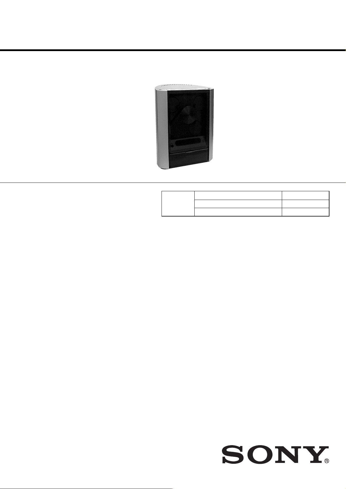
HCD-EX5
Amplifier section
For the U.S. model
AUDIO POWER SPECIFICATIONS
POWER OUTPUT AND TOTAL
HARMONIC DISTORTION:
With 4 ohms loads, both channels driven, from
120 - 10,000 Hz; rated 12 watts per channel
minimum RMS power, with no more than 10%
total harmonic distortion from 250 milli watts
to rated output.
North American model:
Continuous RMS power output (Reference):
15 + 15 W
(4 ohms at 1 kHz, 10%
THD)
European model:
DIN power output (Rated):12 + 12 W
(4 ohms at 1 kHz, DIN)
Continuous RMS power output (Reference):
15 + 15 W
(4 ohms at 1 kHz, 10%
THD)
Music power output (Reference):
15 + 15 W
Other models:
The following measured at 220 V AC, 60 Hz
DIN power output (Rated):
12 + 12 W
(4 ohms at 1 kHz, DIN,
110 V – 240 V AC)
Continuous RMS power output (Reference):
15 + 15 W
(4 ohms at 1 kHz, 10%
THD, 110 V – 240 V AC)
Inputs
PC/TAPE/MD IN (stereo mini jack):
voltage 450 mV (MD)/
250 mV (PC/TAPE),
impedance 47 kilohms
AM tuner section
Tuning range
Pan-American model: 530 – 1,710 kHz
(with the interval set at
10 kHz)
531 – 1,710 kHz
(with the interval set at
9kHz)
European model: 531 – 1,602 kHz
(with the interval set at
9kHz)
Other models: 530 – 1,710 kHz
(with the interval set at
10 kHz)
531 – 1,602 kHz
(with the interval set at
9kHz)
Antenna AM loop antenna, external
antenna terminal
Intermediate frequency 450 kHz
Outputs
PC/TAPE/MD OUT (stereo mini jack):
voltage 250 mV,
impedance 1 kilohm
PHONES (stereo mini jack):
accepts headphones with
an impedance of 8 ohms
or more
OPTICAL CD DIGITAL OUT (Supported sampling
frequency: 44.1 kHz)
CD player section
System Compact disc and digital
audio system
Laser Semiconductor laser
(λ = 795 nm)
Emission duration:
continuous
Frequency response 2 Hz – 20 kHz
Tuner section
FM stereo, FM/AM superheterodyne tuner
FM tuner section
Tuning range
North American model: 87.5 – 108.0 MHz
(100-kHz step)
Other models:
87.5
– 108.0 MHz
(50-kHz step)
Antenna FM wire antenna
Antenna terminals
75 ohms unbalanced
Intermediate frequency 10.7 MHz
SERVICE MANUAL
Ver 1.1 2003. 12
This set is the tuner, CD and amplifier
section in CMT-EX5
CD
SECTION
SPECIFICATIONS
US Model
Canadian Model
AEP Model
UK Model
E Model
Australian Model
Chinese Model
Model Name Using Similar Mechanism NEW
CD Mechanism Type CDM71C-31BD63A
Base Unit Type BU-31BD63A
9-874-036-02
2003L16-1
© 2003.12
Sony Corporation
Home Audio Company
Published by Sony Engineering Corporation
MICRO Hi-Fi COMPONENT SYSTEM
— Continued on next page —
Page 2
HCD-EX5
General
Power requirements
North American model: 120 V AC, 60 Hz
European model: 230 V AC, 50/60 Hz
Mexican model: 120 V AC, 60 Hz
Australian model: 220 – 240 V AC,
Korean model: 220 V AC, 60 Hz
Chinese model: 220 V AC, 50/60 Hz
Other models: 110 – 240 V AC,
Power consumption
European model: See the nameplate
Other models: See the nameplate
Dimensions (w/h/d) Approx. 186 × 235 ×
Mass Approx. 3.0 kg
Design and specifications are subject to change
without notice.
50/60 Hz
50/60 Hz
0.25 W (at the Power
Saving Mode)
157 mm incl. projecting
parts and controls
SAFETY CHECK-OUT
After correcting the original service problem, perform the
following safety checks before releasing the set to the customer:
Check the antenna terminals, metal trim, “metallized” knobs, screws,
and all other exposed metal parts for A C leakage. Check leakage as
described below.
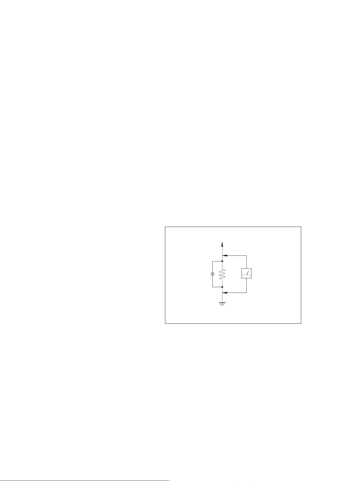
LEAKAGE
The A C leakage from any e xposed metal part to earth ground and
from all exposed metal parts to any exposed metal part having a
return to chassis, must not exceed 0.5 mA (500 microamperes).
Leakage current can be measured by any one of three methods.
1. A commercial leakage tester, such as the Simpson 229 or RCA
WT -540A. Follo w the manufacturers’ instructions to use these
instruments.
2. A battery-operated AC milliammeter. The Data Precision 245
digital multimeter is suitable for this job.
3. Measuring the voltage drop across a resistor by means of a
VOM or battery-operated A C voltmeter . The “limit” indication
is 0.75 V, so analog meters must have an accurate low-v olta ge
scale. The Simpson 250 and Sanwa SH-63Trd are e xamples of
a passive VOM that is suitable. Nearly all battery operated
digital multimeters that have a 2V AC range are suitable. (See
Fig. A)
To Exposed Metal
Parts on Set
AC
0.15 µF
Fig. A. Using an A C v oltmeter to check A C leakage.
1.5 kΩ
Earth Ground
Voltmeter
(0.75 V)
2
Page 3

TABLE OF CONTENTS
1. SERVICING NOTES ······················································· 4
2. GENERAL ·········································································· 5
3. DISASSEMBLY ································································ 8
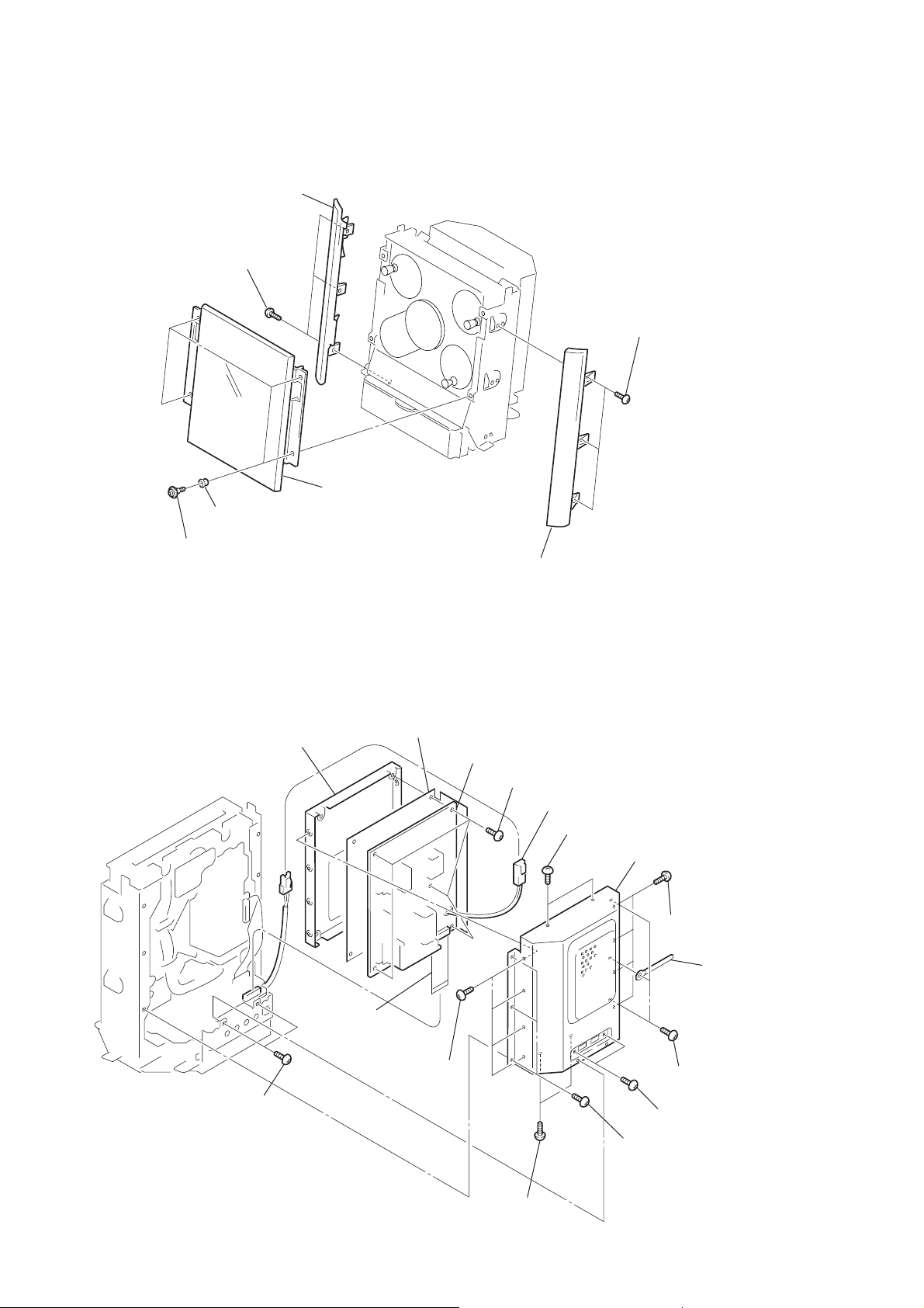
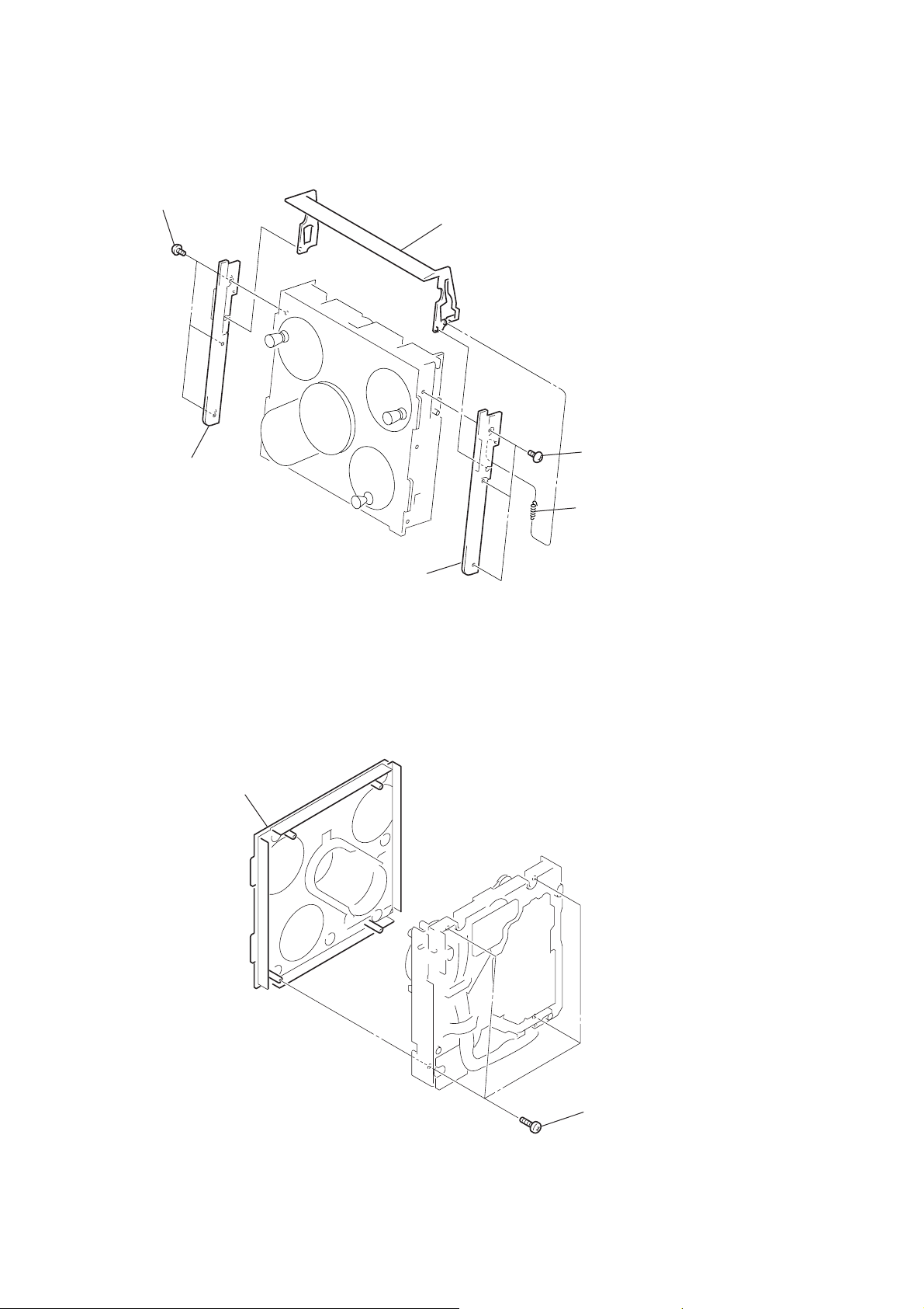
3-1. Case ··············································································· 9
3-2. OC Boad,OS Boad ························································ 9
3-3. Glass Windo w Assy (U) ·············································· 10
3-4. POWER Board ···························································· 10
3-5. BD Board····································································· 11
3-6. MAIN Board, Tunner ·················································· 11
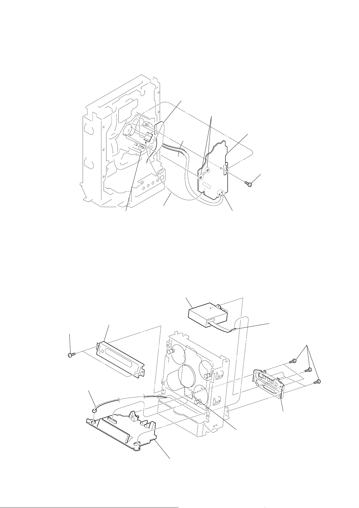
3-7. CD Mechanism (CDM71C-31BD63A)·······················12
3-8. Base Unit(BU-31BD63A) ··········································· 12
3-9. Holder Assy, Sled Motor Assy (M102) ······················· 13
3-10.Case Button Assy, LID Board ····································· 13
3-11.LID (CD) ····································································· 14
3-12.Ornament (Mecha Panel)············································· 14
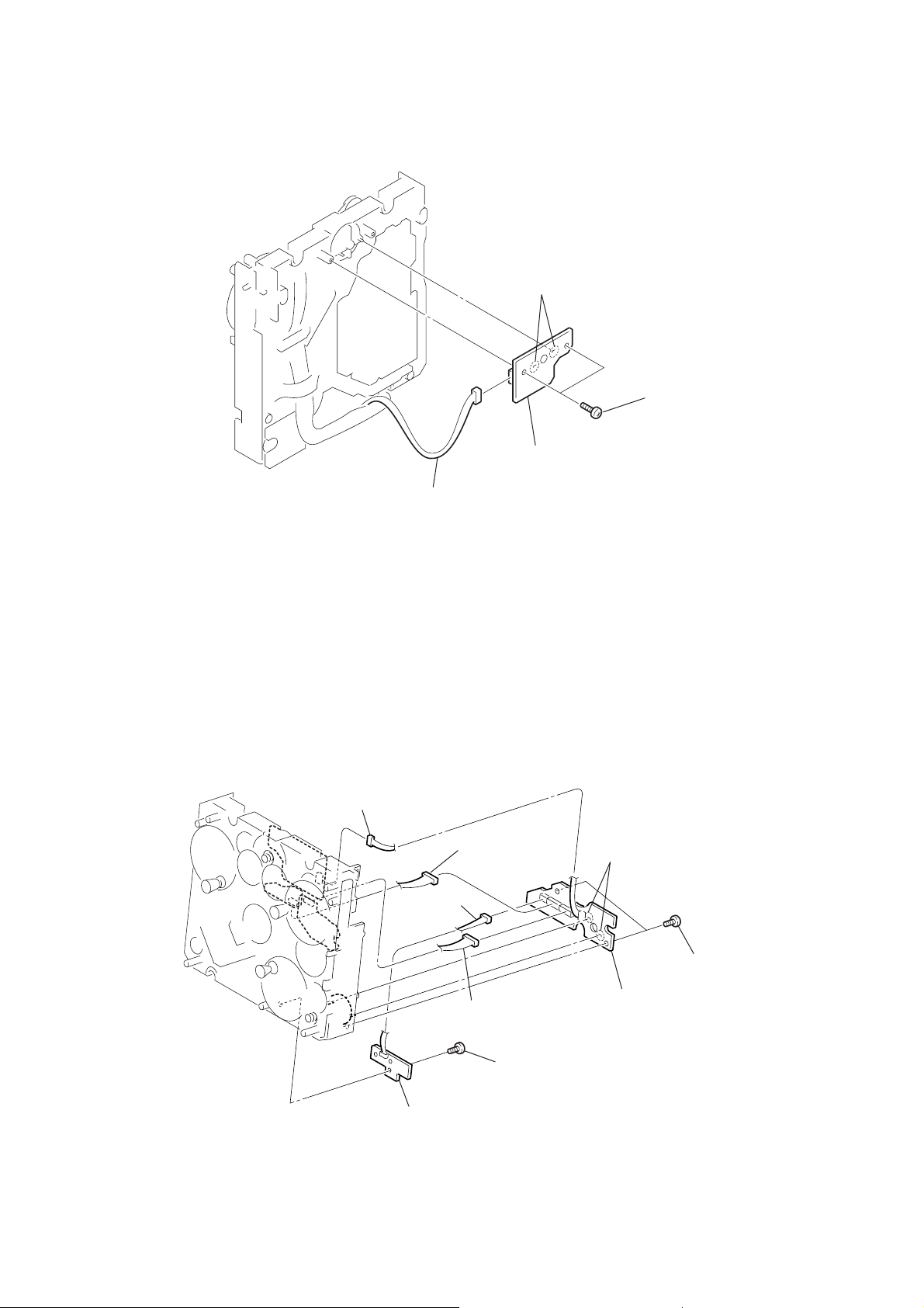
3-13.L.MOTOR Board························································· 15
3-14.C MOTOR Board, L.SENSOR Board························· 15
3-15.ENCODER Board, D.SENSOR Board ·······················16
3-16.RTR Pulley Assy, RTL Pulley Assy,
Belt (CDM71), Belt (Roller) (L) ································· 17
3-17.SPT Pulley Assy, Gear (RT) Assy, Gear (KT),
Belt (CDM71) ····························································· 19
4. TEST MODE····································································21
HCD-EX5
6. DIAGRAMS······································································ 25
6-1. Block Diagrams··························································· 25
6-2. Circuit Boards Location ·············································· 28
6-3. Schematic Diagram – BD Board – ······························29
6-4. Printed Wiring Board – BD Board (Side A) – ············· 30
6-5. Printed Wiring Board – BD Board (Side B) – ············· 31
6-6. Schematic Diagram – MAIN Section (1/2) – ·············· 32
6-7. Schematic Diagram – MAIN Section (2/2) – ·············· 33
6-8. Printed Wiring Board – MAIN Board (Side A) –········ 34
6-9. Printed Wiring Board – MAIN Board (Side B) – ········ 35
6-10.Printed Wiring Board – PANEL Section (Side A) –····36
6-11.Printed Wiring Board – PANEL Section (Side B) –···· 37
6-12.Schematic Diagram – MOTOR Section – ···················38
6-13.Printed Wiring Board – MOTOR Section – ················ 39
6-14.Printed Wiring Board – POWER Board (Side A) – ···· 40
6-15.Printed Wiring Board – POWER Board (Side B) – ···· 41
6-16.Schematic Diagram – POWER Section – ···················42
6-17.IC Pin Function Description········································ 43
7. EXPLODED VIEWS ······················································ 47
7-1. Case Section ································································ 47
7-2. Chassis Section-1 ························································48
7-3. Chassis Section-2 ························································49
7-4. Mechanism Section(CDM71C-31BD63A)-1·············· 50
7-5. Mechanism Section(CDM71C-31BD63A)-2·············· 51
7-6. Base Unit (BU-31BD63A) ·········································· 52
5. ELECTRICAL ADJUSTMENTS ······························· 24
8. ELECTRICAL PARTS LIST ······································· 53
3
Page 4
HCD-EX5
SECTION 1
SERVICING NOTES
NOTES ON HANDLING THE OPTICAL PICK-UP
BLOCK OR BASE UNIT
The laser diode in the optical pick-up block may suffer electrostatic
break-down because of the potential difference generated by the
charged electrostatic load, etc. on clothing and the human body.
During repair, pay attention to electrostatic break-down and also
use the procedure in the printed matter which is included in the
repair parts.
The flexible board is easily damaged and should be handled with
care.
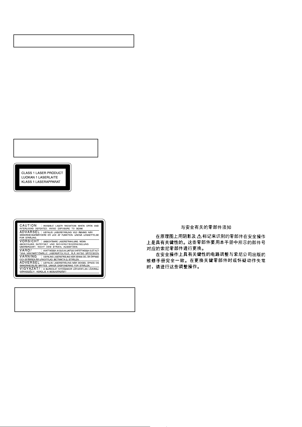
NOTES ON LASER DIODE EMISSION CHECK
The laser beam on this model is concentrated so as to be focused on
the disc reflective surface by the objective lens in the optical pickup block. Therefore, when checking the laser diode emission,
observe from more than 30 cm away from the objective lens.
Laser component in this product is capable
of emitting radiation exceeding the limit for
Class 1.
This appliance is classified as a CLASS 1 LASER product. The
CLASS 1 LASER PRODUCT MARKING is located on the rear
exterior.
Notes on chip component replacement
•Never reuse a disconnected chip component.
• Notice that the minus side of a tantalum capacitor may be
damaged by heat.
Flexible Circuit Board Repairing
•Keep the temperature of soldering iron around 270˚C
during repairing.
• Do not touch the soldering iron on the same conductor of the
circuit board (within 3 times).
• Be careful not to apply force on the conductor when soldering
or unsoldering.
ATTENTION AU COMPOSANT AYANT RAPPORT
À LA SÉCURITÉ!
LES COMPOSANTS IDENTIFÉS P AR UNE MARQUE 0 SUR LES
DIAGRAMMES SCHÉMA TIQUES ET LA LISTE DES PIÈCES SONT
CRITIQUES POUR LA SÉCURITÉ DE FONCTIONNEMENT. NE
REMPLACER CES COMPOSANTS QUE PAR DES PIÈSES SONY
DONT LES NUMÉROS SONT DONNÉS DANS CE MANUEL OU
DANS LES SUPPÉMENTS PUBLIÉS PAR SONY.
SAFETY-RELATED COMPONENT WARNING!!
COMPONENTS IDENTIFIED BY MARK 0 OR DOTTED LINE WITH
MARK 0 ON THE SCHEMATIC DIAGRAMS AND IN THE PARTS
LIST ARE CRITICAL TO SAFE OPERATION. REPLACE THESE
COMPONENTS WITH SONY PARTS WHOSE PART NUMBERS
APPEAR AS SHOWN IN THIS MANUAL OR IN SUPPLEMENTS
PUBLISHED BY SONY.
This caution
label is
located inside
the unit.
CAUTION
Use of controls or adjustments or performance of procedures
other than those specified herein may result in hazardous radiation
exposure.
4
Page 5
Main unit
SECTION 2
GENERAL
HCD-EX5
This section is extracted
from instruction manual.
ALPHABETICAL ORDER
A – Q
Disc slot 2 (23)
Display window 4
DISPLAY qa (16, 19, 20)
FUNCTION 0 (9 - 13, 15, 22,
24)
R – Z
Remote sensor qs
TUNER/BAND 9 (13 - 15, 24)
TUNING +/– 6 (13 -15)
VOLUME +/– 5 (18)
BUTTON DESCRIPTIONS
@/1 (power) 1
Z 3
./> 6
m/M 6
x 7
NX 8
To open the front cover, push
down on the knob under the
display window.
5
Page 6
HCD-EX5
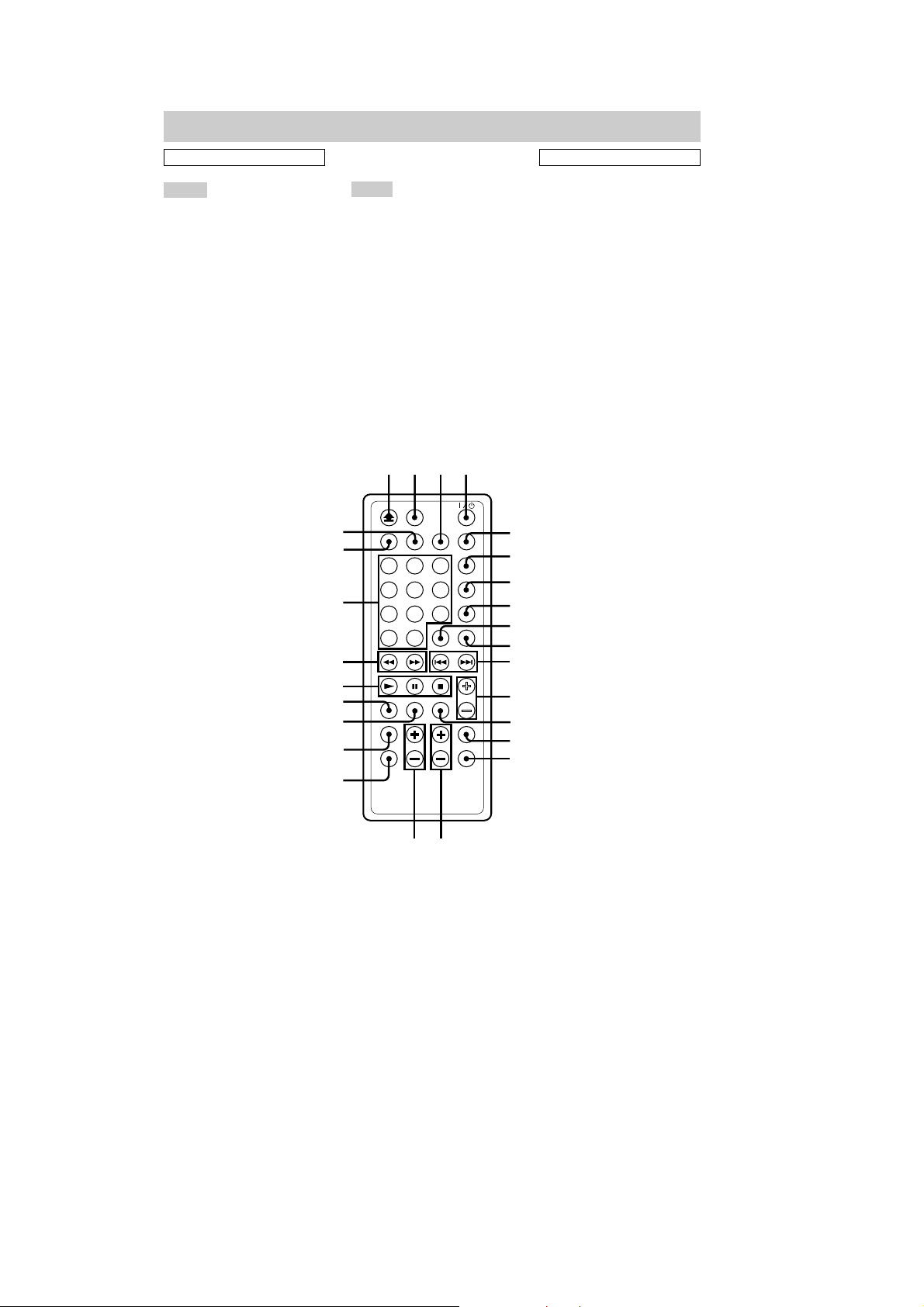
Remote control
ALPHABETICAL ORDER
A – K
BASS +/– qj (17)
CD N ws (9 - 11, 23)
CLEAR 9 (10 - 12, 16)
CLOCK/TIMER SELECT 6
(19)
CLOCK/TIMER SET 7 (8, 18)
CURSOR T/t wd (8, 12)
DIMMER qk (19)
DISPLAY wg (16, 19, 20)
DSG qf (17)
ENTER/YES 8 (8, 10, 12 - 14,
16, 18, 19, 22)
FM MODE qd (15, 24)
FUNCTION ql (9 - 13, 15, 22,
24)
L – Z
Letter/Number buttons wf (10,
12, 15)
MENU/NO q; (12 - 14, 16, 22)
NAME EDIT/SELECT 3 (11,
16)
PLAY MODE w; (9 - 11, 13, 23,
25)
REPEAT qd (10)
SCROLL 5 (12, 20)
SLEEP 2 (17)
SURROUND qg (17)
TIME wh (11, 20)
TREBLE +/– qh (17)
TUNER BAND wa (13 -15)
TUNING MODE w; (13 - 15)
VOL +/– qs (18)
1 234
wh
wg
wf
wd
ws
wa
w;
ql
qk
BUTTON DESCRIPTIONS
Z 1
@/1 (power) 4
./> qa
+/– qa
X ws
x ws
m/M wd
5
6
7
8
9
0
qa
qs
qd
qf
qg
qhqj
6
Page 7
HCD-EX5
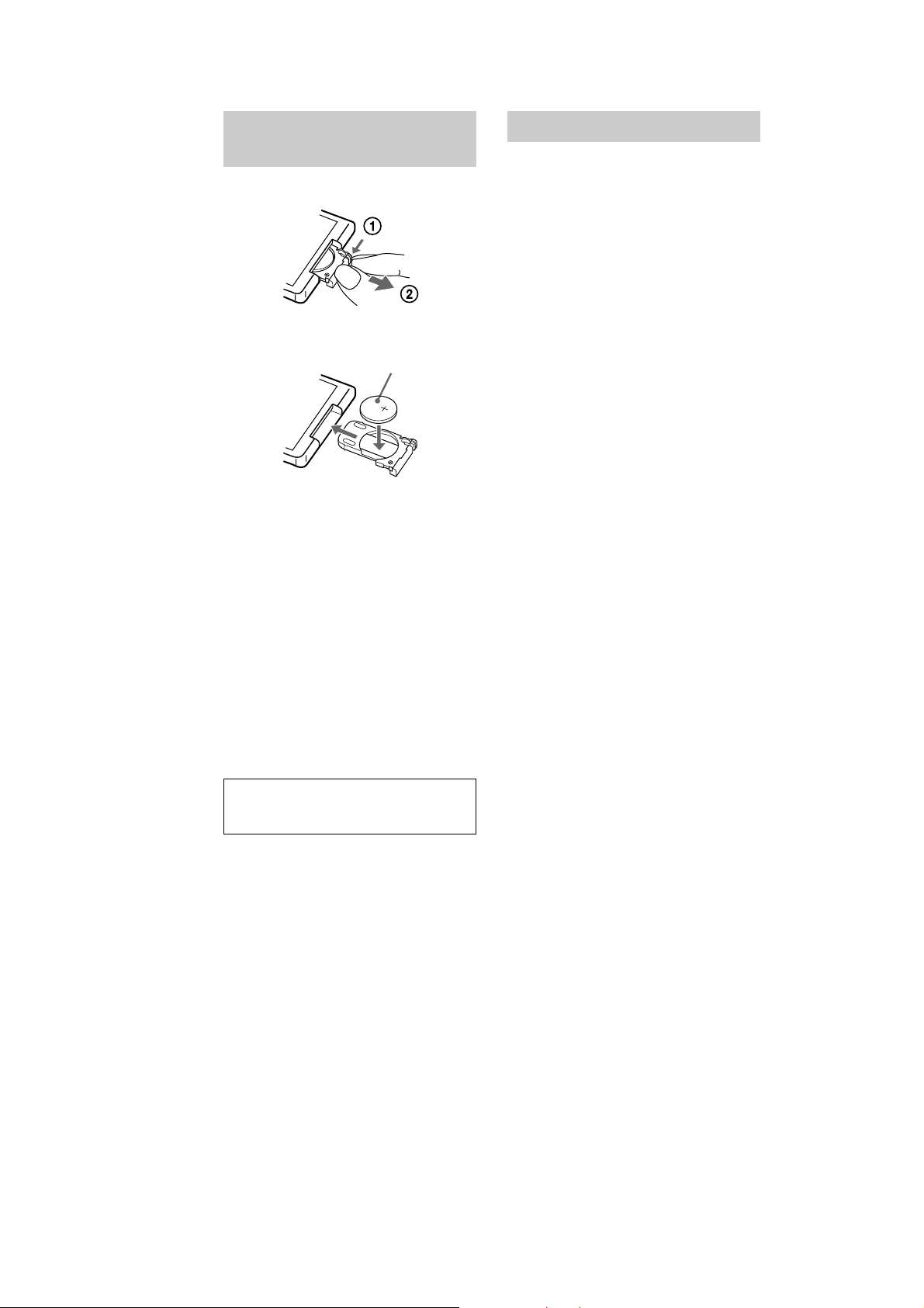
Replacing the battery in
the remote
1
Slide out and remove the battery case.
2
Insert a new lithium battery CR2025
with the + side facing up.
A lithium battery CR2025
3
Slide the battery case back in.
Tip
When the remote no longer operates the system,
replace the battery with a new one.
Note
If you do not use the remote for a long period of time,
remove the battery to avoid possible damage from
battery leakage and corrosion.
Notes on lithium battery
• Keep the lithium battery out of the reach of
children. Should the battery be swallowed,
immediately consult a doctor.
• Wipe the battery with a dry cloth to assure a good
contact.
• Be sure to observe the correct polarity when
installing the battery.
• Do not hold the battery with metallic tweezers,
otherwise a short-circuit may occur.
Setting the clock
1
Turn on the system.
2
Press CLOCK/TIMER SET on the
remote.
The day indication flashes.
3
Press . or > on the remote
repeatedly to set the day, then press
ENTER/YES on the remote.
The hour indication flashes.
4
Press . or > on the remote
repeatedly to set the hour, then press
ENTER/YES on the remote.
The minute indication flashes.
5
Press . or > on the remote
repeatedly to set the minuite, then
press ENTER/YES on the remote.
If you made a mistake
Press TCURSOR or CURSORt on the remote
repeatedly until the indication you want to change
(day, hour, minuite) flashes, and then change the
setting.
To adjust the clock
1
Press CLOCK/TIMER SET on the remote.
2
Press . or > on the remote
repeatedly to select “CLOCK SET?”, then
press ENTER/YES on the remote.
3
Do the same procedures as steps 3 to 5
above.
WARNING
Battery may explode if you mistreated.
Do not recharge, disassemble or dispose of in fire.
7
Page 8
HCD-EX5
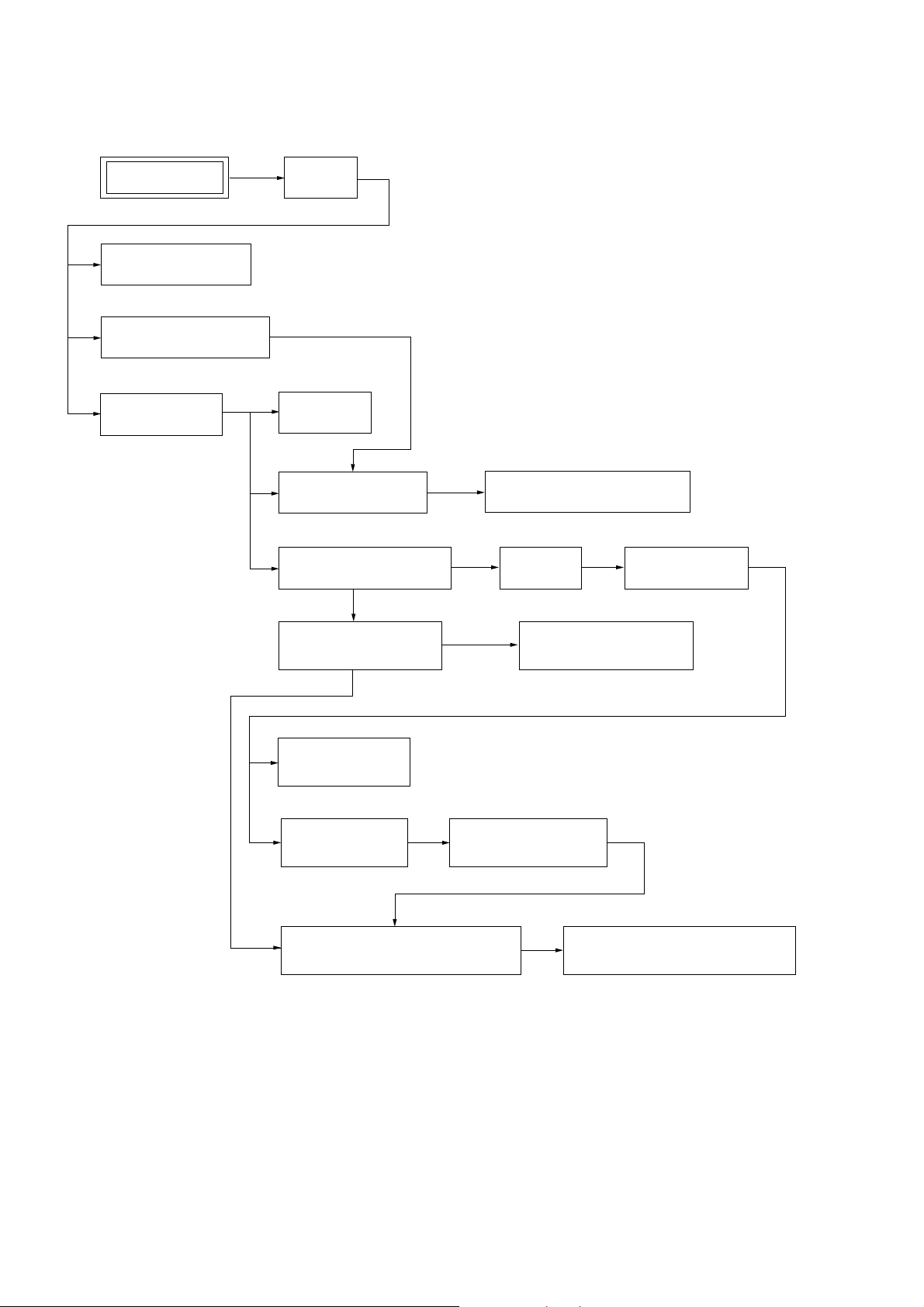
SECTION 3
DISASSEMBLY
• The equipment can be removed using the following procedure.
SET (HCD-EX5) CASE
OC BOARD,OS BOARD
GLASS WINDOW ASSY (U)
POWER BOARD
BD BOARD
MAIN BOARD,TUNNER
CD MECHANISM
(CDM71C-31BD63A)
BASE UNIT (BU-31BD63A)
C MOTOR BOARD,
L.SENSOR BOARD
L.MOTOR BOARD
CASE BUTTON ASSY,LID BOARD
LID(CD)
HOLDER ASSY ,
SLED MOTOR ASSY (M102)
ENCODER BOARD,
D.SENSOR BOARD
(MECHA PANEL)
ORNAMENT
RTR PULLEY ASSY,RTL PULLEY ASSY,
BELT (CDM71), BELT (ROLLER) (L)
SPT PULLEY ASSY,GEAR (RT)ASSY,
GEAR (KT), BELT (CDM71)
8
Page 9
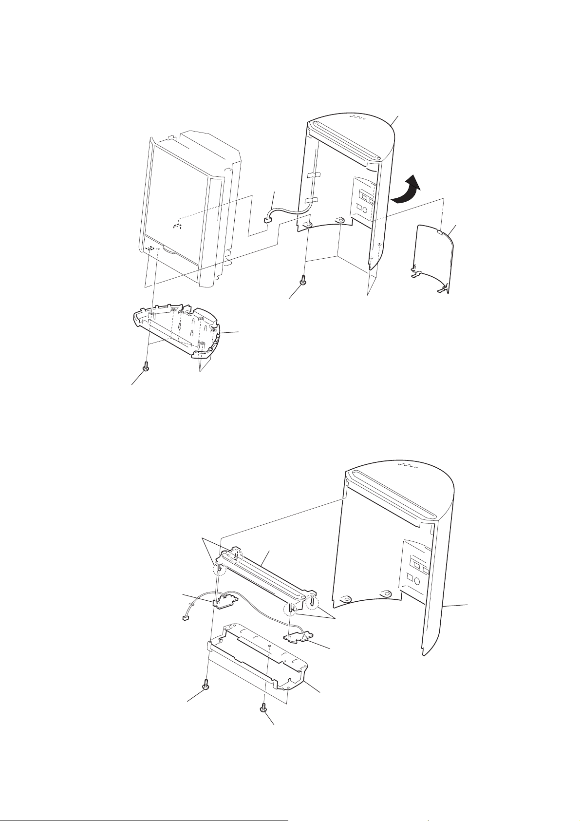
Note : Follow the disassembly procedure in the numerical order given.
e
3-1. Case
7
HCD-EX5
case
2
six screws (+BVTP 3
3-2. OC Boad,OS Boad
× 8
6
c
onnector
(CN621)
4
four
screws (+BVTP 3
3
cover (bottom)
)
× 8
)
5
1
cover (back)
6
OS board
1
5
two claws
two
screws (+BTP 2.6
× 8
4
guide disc assy
cas
7
two claws
8
OC board
3
bracket
)
2
screw (+BTP 2.6
× 8
)
9
Page 10
HCD-EX5
)
3-3. Glass Window Assy (U)
4
retainer plate
3
t
hree screws (+BVTP 3
(L)
× 8
)
1
t
hree screws (+BVTP 3
× 8
)
3-4. POWER Board
5
6
four bushings (bracket)
four
step
screws (slider)
qf
shield (lower)
7
glass
window assy (U)
qg
insulator (power 1)
qh
2
retainer plate
POWER board
qd
five
screws (+BVTP 3
6
(R)
c
onnector
7
two
screws (+BVTP 3
× 8
)
qs
shield (upper)
qa
four
(+BVTP 3
× 8
screws
)
× 8
)
10
1
two
screws
(+BVTP 3
× 8
5
(15 core)
)
f
lat type wire
q;
(+BVTP 3
four
screws
× 8
)
8
(+BVTP 3
two
screws
× 8
3
clamp
2
three
screws
screws
)
× 8
× 8
)
(+BVTP 3
9
two
(+BVTP 3
4
three
(+BVTP 3
)
screws
× 8
Page 11
3-5. BD Board
)
1
f
lat type wire (23 core)
2
(BLK)
(RED)
Remove solder (two portions ).
7
BD board
4
screw (+B 2
HCD-EX5
× 4
)
3-6. MAIN Board, Tunner
1
two
screws
(+BVTP 3
× 8
2
)
5
h
ook
f
ront panel assy
6
flxible
board
6
3
Remove solder (two portions ).
tunner
5
f
lat type wire
(11 core or 15 core)
3
seven
screws (+BVTP 3
× 8
7
connector
(CN601)
9
MAIN board
8
f
lat type wire
(23 core)
4
back panel
11
Page 12
HCD-EX5
)
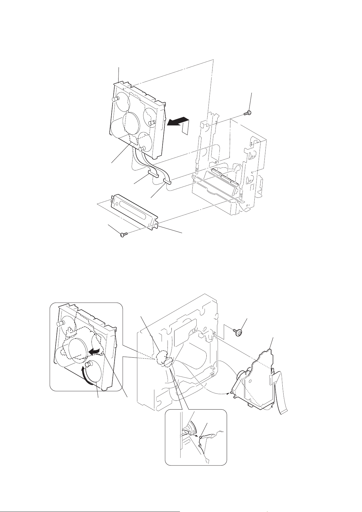
3-7. CD Mechanism (CDM71C-31BD63A)
7
CD mechanism (CDM71C-31BD63A)
3
f
lat type wire
(23 core)
4
connector (CN302)
6
four
screws (+BVTP 3
× 8
)
5
connector (CN303)
1
two
screws (+BVTP 3
× 8
)
3-8. Base Unit(BU-31BD63A)
Rotate the SPT pulley assy in the direction of to move the Base unit shaft
forward.
1
1
cam (A)
2
f
ront panel assy
2
screw
(+PTPWH M2.6)
5
base unit
(BU-31BD63A
12
SPT pulley assy
shaft
4
3
shaft
Page 13
HCD-EX5
3-9. Holder Assy, Sled Motor Assy (M102)
9
two screws
(+PTPWH M2.6)
holder assy
7
coil spring (C) (holder)
5
BD board
q;
qs
screw
(+P 2
h
×
ook
8
screw
(+PTPWH M2.6)
qa
base unit
4
flxible
board
qd
sled motor assy (M102)
3)
6
coil spring (B) (holder)
1
Remove solder
(two portions ).
(RED)
(BLK)
3-10. Case Button Assy, LID Board
7
four
screws (+BVTP 3
qd
two
screws
(+KTP 2.6
× 6
)
8
3
screw
(+BTP 2
6
4
two
(+BVTP 3
× 8
)
× 8
)
frame (L)
screws
8
× 8
2
Remove solder
(two portions ).
)
5
two
hooks
3
frame (R)
2
two
hooks
qf
glass window assy (L)
q;
three
screws (+BTP 2.6
9
case button assy
qa
LID board
× 8
)
qs
two
screws (+KTP 2.6
× 6
1
)
screw (+BVTP 3
× 8
)
13
Page 14
HCD-EX5
)
)
3-11. LID (CD)
4
three
(+BVTT 2.6
5
screws
× 4
)
retainer plate (L)
6
LID (CD)
2
three
(+BVTT 2.6
screws
×
4
)
3-12. Ornament (Mecha Panel)
2
ornament (mecha panel)
3
retainer plate (R)
1
tension coil spring (CD door
14
1
four
screws
(+BVTP 2.6
×
8
Page 15
3-13. L.MOTOR Board
)
)
1
Remove solder (two portions ).
4
L.MOTOR board
2
two
screws
(+BVTP 2.6
×
HCD-EX5
8
3
(CN711)
3-14. C MOTOR Board, L.SENSOR Board
3
connector
(CN711)
5
(CN753)
connector
c
onnector
4
c
onnector
(CN754)
1
Remove solder
(two portions ).
6
c
onnector
(CN755)
9
L.SENSOR board (R)
8
screw
(+BTP M 2.6
×
7
6)
2
two screws
(+BTP M 2.6
C MOTOR board
×
6
15
Page 16
HCD-EX5
Ver 1.1 2003.12
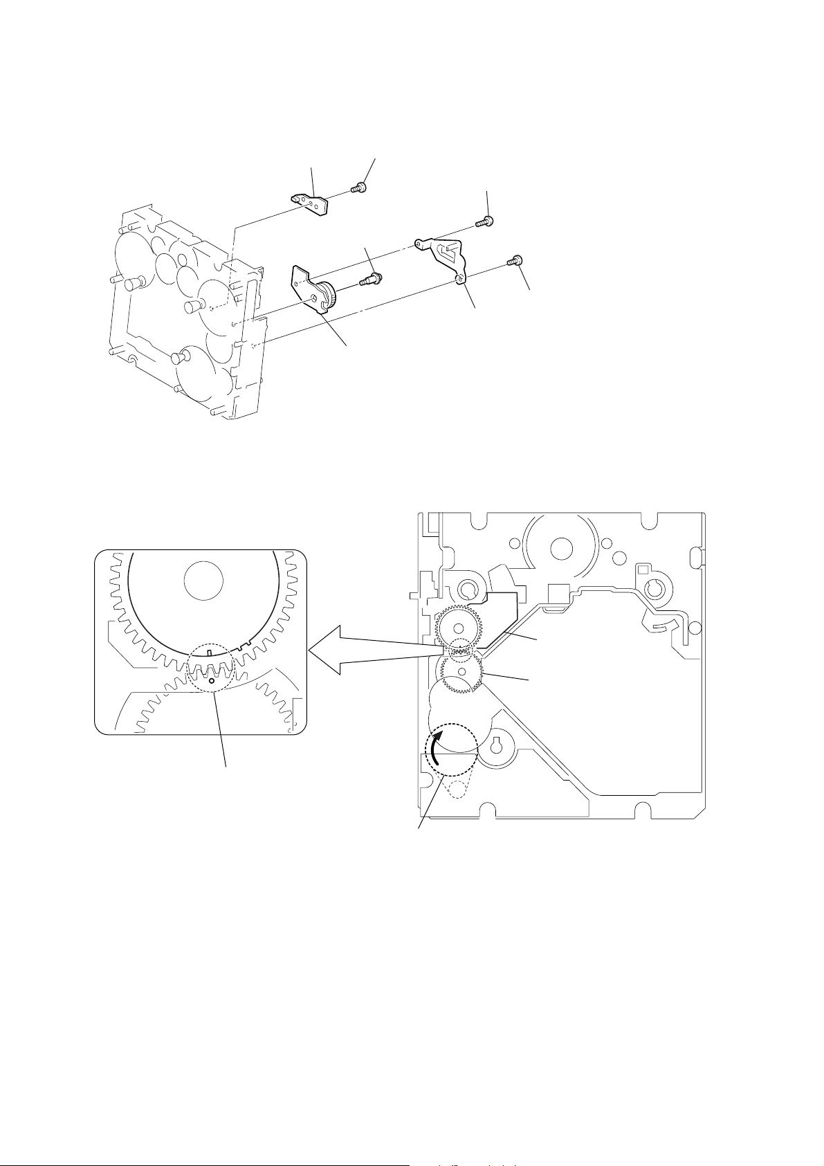
3-15. ENCODER Board, D.SENSOR Board
7
D.SENSOR board
4
6
(+BTP 2.6
screw (+PWH 2
5
ENCODER
screw
×
6)
×
6)
3
cover (encoder)
board
2
screw (+BTP 2.6
1
(+BTP 2.6
screw
× 8
)
×
6)
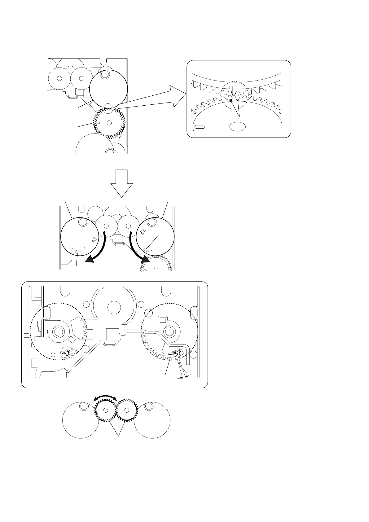
PRECAUTION DURING ENCODER board INSTALLATION
Rotate the pulley (LDG2) until the mark of the cam (A) becomes visible.
Install the ENCODER board in the way that it is sandwiched by
the cut-outs of the ENCODER board.
pulley (LDG2)
ENCODER board
cam (A)
16
Page 17
3-16. RTR Pulley Assy, RTL Pulley Assy, Belt (CDM71), Belt (Roller) (L)
6
screw
7
D.SENSOR board
(+BTP 2.6
5
ENCODER
(When installing it, see the ENCODER board item.)
×
6)
3
cover (encoder)
4
screw (+PWH 2
board
2
screw (+BTP 2.6
×
1
screw
(+BTP 2.6
6)
× 8
×
HCD-EX5
)
6)
qf
RTL pulley assy
9
qg
gear (S1)
c
law
qh
belt (CDM71)
q;
8
pulley (RTR) assypulley (RTL) assy
c
law
q;
RTL pulley assy
qd
RTR pulley assy
qs
RTR pulley assy
qj
belt (ROLLER) (L)
qa
17
Page 18
HCD-EX5
PRECAUTION DURING PULLEY (RTR) ASSY, PULLEY (RTL) ASSY INSTALLATION
pulley (RTR) assy
pulley (RTR) assy
gear (S2)
(9 o'clock position)
pulley (RTL) assy
claw
marks of the gear (S2)
Place the holes of the gear (S2) at the 9 o'clock position and install
the pulley (RTR) assy.
Install it in the way that the gear of the cut-out portion as shown is located in
between the marks of the gear (S2).
pulley (RTR) assy
claw
Then install the pulley (RTL) assy in the way that it can perform
the symmetrical movement with the pulley (RTR) assy.
Then lock both claws.
pulley (RTR) assy
pulley (RTL) assy
Confirm that the pulley (RTR) contacts the claws.
Opposite to it, the pulley (RTL) assy must
have clearance of 1 to 2 mm with the claw.
It should contact with claw.
If clearance is too large or it contacts with claw,
adjustment is necessary.
claw
1 to 2 mm
Method of adjustment is as follows.
Raise the right gear (S1) a little and perform adjustment
by moving the left gear (S1).
gear(S1)
18
Page 19
3-17. SPT Pulley Assy, Gear (RT) Assy, Gear (KT), Belt (CDM71)
HCD-EX5
3
2
SPT pulley assy
4
gear (KT)
gear (RT) assy
Rotate the SPT pulley assy in the direction of , and remove your hands
at the position where the shaft agrees with the hole shape on the chassis.
SPT pulley assy
5
belt (CDM71 )
When installing, align the protruded portion of the KT gear with groove of the SPT
pulley assy.
1
1
19
Page 20

HCD-EX5
)
PRECAUTION DURING gear (RT) assy, gear (KT) INSTALLATION
lever (ST)
cam (A)
pulley (LDG2)
Rotate the pulley (LDG2) until it reaches the position
where the cam (A) contacts with the lever (ST).
gear (S2)
torsion spring (M)
The boss that is closest to the inside
gear (KT
Install the gear (KT) and position it so that the boss
that is closest to the inside is located at the 9 o'clock position.
gear (S2)
gear (RT) assy
Install the gear (RT) assy so that the two bosses are aligned
in between the torsion spring (M).
Install the gear (S2) so that its hole is located at the 9 o'clock position.
gear (RT) assy
Confirm that the gear (S2) mark is located
in between the gear (RT) assy marks.
20
Page 21

SECTION 4
TEST MODE
HCD-EX5
[Key Check Mode]
* Keyboard check.
Procedure:
1. Press the ?/1 button to turn the set ON.
2. To enter the test mode, press three buttons Z , DISPLAY ,
and > simultaneously.
3. In the key check mode, the message “KEY00” is displayed.
Each time a button is pressed, “KEY00” value increases.
However, once a button is pressed, it is no longer taken into
account.
4. To e xit from this mode, press three b uttons Z , DISPLAY ,
and > simultaneously.
[Version Display Mode]
* The version or destination is displayed.
Procedure:
1. Press the ?/1 button to turn the set ON.
2. To enter the test mode, press three buttons Z , DISPLAY ,
and x simultaneously.
3. The model name and destination are displayed.
4. Press the DISPLAY button. The STR version is displayed.
5. Press the DISPLA Y button again. The CD v ersion is displayed.
6. Press the DISPLAY button. The model name and destination
are displayed again.
7. To exit from this mode, press the ?/1 button to turn off the set.
[LCD Test Mode]
* All LCD segments are tested.
Procedure:
1. Press the ?/1 button to turn the set ON.
2. To enter the test mode, press three buttons Z , DISPLAY ,
and . simultaneously.
3. The following segments are turned on.
PROGRAM REPEAT SURR
SHUFFLE SLEEPPLAY
DISCID3
MP3
ALBUM
TRACK TUNED MONO MANUAL
ALBUM
1
DSG
STEREO AUTO PRESET
c
These segments remain when entering into the LCD test mode.
4. Press the DISPLAY button. All segments are turned off.
5. Press the DISPLA Y b utton. Confirm the pa ttern of segments.
TEXT SLEEPPLAY
PROGRAM SURR
DISCID3 PRESET
1
TUNED MANUAL
[Amp Test Mode]
* Volume level is changed for the amplifier test.
Procedure:
1. Press the ?/1 button to turn the set ON.
2. To enter the test mode, press three buttons Z , DISPLAY ,
and NX simultaneously.
3. V olume lev el is changeable at three steps as “VOLUME MIN”,
“VOLUME 21”, “V OLUME MAX” by pressing V OLUME +
or VOLUME – button.
4. In this test mode, the tuning mode is set to the preset mode.
5. To exit from this mode, press the ?/1 button to turn off the set.
[Forced Reset]
* All micro-processors are forced to reset at the same time.
Procedure:
1. Press the ?/1 button to turn the set ON.
2. Press three buttons Z , FUNCTION , and TUNER/BAND
simultaneously.
3. The message “COLD RESET” is displayed and the set is reset.
Then the set is turned off.
[CD Ship Position]
Procedure:
1. Press the ?/1 button to turn the set ON.
2. Press the FUNCTION button for the setting CD.
3. Press three buttons Z , VOLUME – , and > simulta-
neously.
4. The message “COLD RESET” is displayed and CD is set to
the shipment position. Then the set is turned off.
[Loading Mechanism Lock]
Procedure:
1. Press the ?/1 button to turn the set ON.
2. Press two buttons of x and Z simultaneously for fiv e seconds.
3. The message “LOCKED” is displayed and the loading
mechanism is locked. (Even if exiting from this mode, the
loading mechanism is still locked.)
4. Press two buttons of x and Z simultaneously for five seconds
again.
5. The message “UNLOCKED” is displayed and the loading
mechanism is unlocked.
6. To exit from this mode, press the ?/1 button to turn the set
off.
6. Press the DISPLA Y b utton. Confirm the pa ttern of segments.
MP3
SHUFFLE
ALBUM
TRACK MONO
ALBUM
REPEAT
STEREO AUTO
DSG
c
7. Every pressing of the DISPLA Y button turns on each se gment
one after another in the same order.
8. To e xit from this mode, press the ?/1 button to turn off the set.
[Aging In1 Mode]
Procedure:
1. Press the ?/1 button to turn the set ON.
2. Insert the disc.
3. Select the FUNCTION to CD.
4. To enter the test mode, press three b uttons VOLUME – , NX
and Z simultaneously.
5. Aging operation starts automatically.
6. The CD is out, drawn in and the first track is played. Then the
last track is played.
7. The CD is out again, and the message “AGIN00000001” is
displayed. This value is cycle times of aging operation and
displays hexadecimal data.
8. The CD is drawn in and aging operation is continued.
9. To exit from this mode, press the ?/1 button to turn off the set.
21
Page 22

HCD-EX5
[Aging In Mode]
Procedure:
1. Press the ?/1 button to turn the set ON.
2. Select the FUNCTION to CD.
3. To enter the test mode, press three buttons VOLUME + ,
> and Z simultaneously.
4. Confirm that “dvt AGING” is displayed.
5. Press the Z button.
6. Confirm that “dvt AGING SL” is displayed.
Releasing Method of Test Mode
1. Press the x button to display “dvt AGING”.
2. Press the x button again.
Menu Selection of Aging Selection Mode
1. Select the operation in the menu by pressing the . or
> button.
2. Press the Z button. The menu is selected.
3. Press the x button to return to the menu again.
SELECTION OF AGING AND START “dvt AGING SL”
Y
DISPLAY OF TIMES OF A GING “dvt AGING DP”
Selection of Aging and Start
1. Confirm that “AGING SEL=00” is displayed.
2. Select the aging operation in the menu by pressiing the .
or > button. Normally “00” is suitable.
3. Press the Z button.
4. Aging operation starts automatically.
DISPLAY : “AGING SEL = ##”
## : type of aging
00 : OPEN c CHUCK c the first track playback c the last
track playback c OPEN c CHUCK c
…
01 to 03 : not for service
04 : the first track playback c the last track playback c the
first track playback c
…
05 to o6 : not for service
Display of Times of Aging
1. Confirm that “dvt AGING DP” is diplayed.
2. Press the Z button.
DISPLAY : “AGING********”
******** : 0 to FFFFFFFF (hexadecimal) times of aging cycle executed
Releasing Method of Aging Operation
Press the ?/1 button to turn off the set.
[Error History Display Mode]
Procedure:
Setting Method of Test Mode
1. Press the ?/1 button to turn the set ON.
2. Select the FUNCTION to CD.
3. T o enter the test mode, press three buttons Z , V OLUME + ,
and NX simultaneously.
4. Confirm to display “dvt ERR CODE”.
5. Press the Z button.
Releasing Method of Test Mode
1. Press the x button to display “dvt ERR CODE”.
2. Press the x button.
Menu Selection of Error History Display Mode
1. Select the operation in the menu by pressing the . or >
button.
2. Press the Z button. The menu is selected. If returning to the
menu again, press the x button.
DISPLAY OF TIMES OF ERROR
DISPLAY OF MECHANISM ERROR HISTORY
RESET OF MECHANISM ERROR HISTORY
RESET OF ERROR HISTORY
RESET OF NO DISC ERROR HISTORY
DISPLAY OF NO DISC ERROR HISTORY
" Emc=**Edc=## "
" dvt ECODE MEC "
" dvt ECNT0 MEC "
" dvt ECNT0 ALL "
" dvt ECNT0 BU "
" dvt ECODE BU "
Display of Times of Error
* Number of times of mechanism error and no disc error is displayed
in hexadecimal.
DISPLAY : “ Emc=**Edc=## “
** : number of times of mechanism error (hexadecimal)
## : number of times of no disc error (hexadecimal)
Display of Mechanism Error History
1. Select the operation in the menu by pressing the . or >
button to display “dvt ECODE MEC”.
2. Press the Z button.
3. Select the mechanism error code by pressing the . or >
button.
22
Page 23

HCD-EX5
DISPLAY : “ E**M##%%0000 “
** : order of mechanism error happens (hexadecimal)
00 : the newest error
09 : the error ten times before
## : completion of an initialization (hexadecimal)
ff : completion
others : not completed
%% : condition of CDM operation when the trouble happened
(hexadecimal)
00 : during an initialization
1x : during opening (x : not fixed)
16 to 19 : during a kick by falure of opening
2x : completion of opening
28 : completion of opening under the condition of no disc
3x : during close request
4x : during open request
5x : during closing
6x : during chucking
80 : during releasing
9x : during operation of BU down
ax : during operation of shutter opening or closing
b0 : during BU up request
c0 : during BU down request
dx : during operation of BU up
0000: fixed
Reset of Mechanism Error History
1. Select the operation in the menu by pressing the . or >
button to display “dvt ECONT0 MEC”.
2. Press the NX button. Mechanism error history is reset.
Display of No Disc Error History
1. Select the operation in the menu by pressing the . or >
button to display “dvt ECODE BU”.
2. Press the Z button.
3. Select the no disc code by pressing the . or > button.
DISPLAY : “ E**D##%%@@&& “
** : order of no disc happens (hexadecimal)
00 : the newest
09 : ten times before
## : description of the trouble (hexadecimal)
01 : focus NG
02 : GFS NG
03 : time-over of starting
04 : continuous unlock of focus
05 : no input of Q-codes in fixed time
%% : condition when the trouble happened (hexadecimal)
01 : during shipment position processing
02 : during power off processing
03 : during processing of initialization
04 : during stop condition
05 : during stop processing
06 : during process of starting
07 : during process of TOC reading
08 : during search operation
09 : during playback
0a : during pause
0b : during playback manual searching
0c : during pause manual searching
@@ : do not care
&& : rotating speed of a disc when the trouble happened
(hexadecimal)
01 : x1
02 : x2 (double speed)
03 : x4
Reset of No Disc Error History
1. Select the operation in the menu by pressing the . or >
button to display “dvt ECONT0 BU”.
2. Press the NX button. No disc error history is reset.
Reset of Error History
1. Select the operation in the menu by pressing the . or >
button to display “dvt ECONT0 ALL”.
2. Press the NX button. Error history is reset.
[Servo Test Mode]
*Error Rate Display
Procedure:
Setting Method of Test Mode
1. Press the ?/1 button to turn the set ON.
2. Insert the disc.
3. Select the FUNCTION to CD.
4. Press the NX button to play the CD.
5. To enter the test mode, press three buttons VOLUME + , x
and Z simultaneously. Confirm that the message “bdt STEST”
is displayed.
6. Press the . or > button to display “dvt ERR RATE”.
7. Press the Z button.
Description of Error Rate
" ****####%%@@&& "
C1 C2 TNO MIN SEC
Releasing Method of Test Mode
1. Press the x button to display “dvt ERR RATE”.
2. Press three buttons V OLUME + , x and Z simultaneously.
[CD Repeat 5 Times Limit Release Mode]
Procedure:
Setting Method of Test Mode
1. Press the ?/1 button to turn the set ON.
2. Select the FUNCTION to CD.
3. Press three buttons Z , VOLUME – and . simulta-
neously.
4. The message “dvt REP LMT” is displayed.
5. Press the Z button.
Releasing Method of Test Mode
1. Press the x button to display “dvt REP LMT”
2. Press the x button.
Selection of Repeat 5 Times Limit ON/OFF
1. Press the . or > button to display “REP LMT ON” or
“REP LMT OFF”.
2. Press the x button to select ON or OFF and “dvt REP LMT”
is displayed.
23
Page 24

HCD-EX5
)
SECTION 5
ELECTRICAL ADJUSTMENTS
CD SECTION
Note :
1. CD Block is basically designed to operate without adjustment.
Therefore, check each item in order given.
2. Use YEDS-18 disc (3-702-101-01) unless otherwise indicated.
3. Use an oscilloscope with more than 10MΩ impedance.
4. Clean the object lens by an applicator with neutral detergent
when the signal level is low than specified value with the
following checks.
RF Level Check
oscilloscope
BD board
TP(RFAC)
TP(DVC)
Procedure :
1. Connect oscilloscope to TP (RFAC).
2. Turned Power switch on.
3. Load a disc (YEDS-18) and playback the number five track.
4. Confirm that oscilloscope waveform is clear and check RF signal
level is correct or not.
Note: Clear RF signal waveform means that the shape “◊” can be
clearly distinguished at the center of the waveform.
Adjustment Location :
[ BD BOARD ] — SIDE A —
IC103
RF signal waveform
VOLT/DIV : 200mV
TIME/DIV : 500ns
level : 1.1 ± 0.3Vp-p
E-F Balance (1 Track jump) Check
oscilloscope
BD board
TP (TE)
TP (DVC)
+
–
Procedure:
1. Connect oscilloscope to TP (TE) and TP (DVC) board.
2. Turned Power switch on.
3. Load a disc (YEDS-18) and playback the number five track.
4. Press the u button. (Becomes the 1track jump mode.)
5. Confirm that the level B and A (DC voltage) on the oscilloscope
waveform.
1 track jump waveform
Center of
waveform
IC101
TP(DVC)
TP(TE)
TP
(RFAC)
B
0V
level=1.3 ±0.6Vp-p
Specification level: x 100=less than ±22%
A
B
Symmetry
24
A (DC voltage
Page 25

HCD-EX5
6-1. Block Diagrams
– CD Section –
OPTICAL PICK-UP
BLOCK
5
VCC
9
PD1
4
PD2
10
I5-10
8
I1-6
6
LD+
11
GND
7
2
VCC
LIMIT IN
SWITCH
FOCUS
COIL
TRACKING
COIL
TR+
SW
TR-
SECTION 6
DIAGRAMS
IC381
OSCILLATOR
23 5
6
• R-CH is omitted due to same as L-CH.
• Signal Path
X381
16.934MHz
IC101
DIGITAL SERVO,
DIGITAL SIGNAL PROCESSOR
IC103
RF AMP
VC
CD+5V
Q101
LD
DRIVE
RV101
PD
F-
F+
M102
SLED
MOTOR
M101
SPINDLE
MOTOR
CD+5V
M
M
27
VC
25
VFC
6
RFAC
A
7
RFDCO
B
8
C
RFDCI
9
D
10
E
11
F
1
LD
SW
19 TE_BAL
2
PD
IC102
MOTOR/COIL DRIVER
47
VO1+
52
VO1-
55
VO2+
56
VO2-
1
VO3+
VO3-
2
VO4-
10
VO4+
5
IN1+
IN2+
IN3+
IN4R
STBY
IN2-
IN3-
71
XTAI
67
50
15
28
29
16FE
17FEI
18TE
12
35
34IN1-
32
31
27
26
24
8
43
39
41
40
26 SSTP
33
34
32
30
25
IC721
L SENSOR
RFAC
RFDC
FE
TE
SE
FFDR
FRDR
TFDR31
TRDR
SFDR29
SRDR
MDP
BCLK
PCMD
LRCK
D OUT
SQSO
SENS
SCLK
SQCK
SCOR
S731
L MOTOR
C MOTOR
66
65
64
4DATA
6CLOK
5XLAT
76
7
8
77
15
2XRST
IC106
42
S741
ROTARY
ENCODER
XRST
IC301
DAC
16
MCLK
1
BCK R-CH
2
DATA
3
LRCK
13
DATA
14
CLK
15
LAT
IC701 (1/2)
MASTER CONTROLLER
54
DACDAT
55
DACCLK
4
DACLAT
CXD-DATA
7
CXD-CLK
8
CXD-XLT
11
15
SUBQ
14
SENSE
17
SQCLK
95
SCOR
BDRST
23
12
PWM1
PWM2
PWM3
LDON
ENC1
ENC2
ENC3
ENC4
L.MTR SW2
C.MTR SW1
OPT SNS2 (L)813
(LO-MTR F)
LOD1POS
(LO-MTR R)
LOD1NEG
(CK-MTR F)
LOD2POS
(CK-MTR R)
LOD2NEG
19
20
13
82
83
84
89
73
72
7
LOUT CD-L
8
ROUT
10
VCOM
22
BDPWR
67
68
69
70
+3.3V
IC301
IC371
IC381
+3.3V
CD+5V
IC302
LPF
6
–
+
5
Q391
RIPPLE
FILTER
Q103,D101
+3.3V
REG
: CD DIGITAL OUT
: CD
7
IC711
LO MOTOR DRIVER
FIN
7
OUT1
OUT2
RIN
9
IC701
CK MOTOR DRIVER
FIN
7
OUT1
OUT2
RIN
9
D OUT
Q781, 782
B+
SWITCH
4
2
4
2
3
CD+5V
M
M
IC371
OPTICAL
OUT
M701
(LO)
M702
(CK)
A
SECTION
CD DIGITAL OUT
OPTICAL
MAIN
CD+5V
Q701
B+
SWITCH
IC731
D SENSOR
80
3
OPT SNS1 (D)
71
DSNSOUT
2525
Page 26

– MAIN Section –
PC/MD/TAPE
FM75Ω
ı
ANTENNA
AM
ı
J101
IN
CD
SECTION
CD-L
A
TUNER PACK
L OUT
R OUT
ST DOUT
ST DIN
ST CLK
ST CE
TUNED
STEREO
ST MUTE
RDS DATA
RDS INT
RDS +5V
• R-CH is omitted due to same as L-CH.
• Signal Path
: FM
: CD
: PC/MD/TAPE(PB)
: PC/MD/TAPE(REC)
R-CH
R-CH
Q401,402
+5V
REG
4
5
6
AEP, UK
+10V
INB1
INC1
IND1
IC121
PRE AMP
CLOCK
22 21
IC631
REMOTE
CONTROL
RECEIVER
S621,622
FUNCTION
KEY
S601,602,615,616
FUNCTION
KEY
S603,611-614
FUNCTION
KEY
DATA
1
INEX1
OUT1
BB A1
BB B1
7
18
16
17
SIRCS
DETECT
X701
32.768kHz
X702
20MHz
D703
Q121
DBFB
SWITCH
IC701 (2/2)
MASTER CONTROLLER
29
GEQ-DATA
GEQ-CLK
30
DIG-AMP-SLEEP
44
PLL-DI(ST UCOM)
45
PLL-DO(UCOM ST)
43
PLL-CLK
46
PLL-CE
49
TUNED
48
STEREO
47
ST-MUTING
50
RDS-DATA
96
RDS-CLK
51
AM
94
SIRCS
(WAKE UP)RM_INIT
93
KEY1
77
(WAKE UP)KEY_INIT
90
78
KEY2
79
KEY3
XT1
35
36
XT2
39
X1
X2
38
D501
HP-MUTE
LINE-MUTING
SPK-RELAY
HP IN
DISP-DATA
DISP-CLK
DISP-CS
DISP-RS
POWER SAVE
DIM0
DIM1
STANDBY LED
AC_CUT
RESET
HCD-EX5
R-CH
Q111
MUTING
Q122
MUTING
Q124
27
28
33
26
24
1
2
57
56
64
31
32
66
91
34
MUTING
SWITCH
Q123
MUTING
SWITCH
Q791
RESET
SWITCH
Q801
LCD601
LIQUID CRYSTAL
DISPLAY
4
SDA
SCL
5
6
CS
RS
7
VDD
Q672,674
DIM
CONTROL
IC501
(HP AMP)
R-CH
2
ST+10V
IC121
Q591
RIPPLE
FILTER
D621
(STANDBY)
`/1
IC791
4 5
RESET
Q691,692
B+
SWITCH
D681 - 684
(BACK LIGHT)
Q792,793
VOLTAGE
DETECT
SYS+5V
A+10V
CD+5V
SYS+5V
3 1
3 1CD+7V
3
D792
D791
IC911
+5V
REG
IC921
+7V
REG
IC931
+10V
REG
IC101
DIGITAL POWER AMP
10
IN1 L-IN
18
FAULT
11
MUTE
17
SLEEP
IC501
HEADPHONE AMP
3
+13.5V
(IC101)
1
IC951
+5.5V
3 1BACKUP+5V
REG
OUTM1
(-)L-
OUTP1
(+)L+
Q952,953
ECO
1
24
26
DELAY
1
D902
IC102
DC CANCEL
R-CH
IC941
ERROR
1
AMP
Q951
SWITCH
3
2
D901
2
D951
MUTING
Q841,842
DETECT
T1
PC1
T51
PC51
DC
Q501
R-CH
LPF
LPF
RY891
RELAY
DRIVE
D10
Q1
B+
SWITCH
Q52
B+
SWITCH
Q51
B+
SWITCH
R-CH
R-CH
Q843
R-CH
Q53
J111
OUT
L
CN801
SPEAKER
R
J501
PHONES
AC IN
IC1
MAIN CONVERTER
D
3
OCP/INH
1
VCC
4
GND
2
FB/OCP
5
R51
BOOT
D53
RESISTOR
IC51
STANDBY
CONVERTER
D
7
D
8
VIN
3
GND
2
S
1
FB/OCP
4
PC/MD/TAPE
2626
Page 27

HCD-EX5
B
These are omitted.
CE
THIS NOTE IS COMMON FOR PRINTED WIRING
BOARDS AND SCHEMATIC DIAGRAMS.
(In addition to this, the necessary note is printed
in each block.)
For schematic diagrams.
Note:
• All capacitors are in µF unless otherwise noted. pF: µµF
50 WV or less are not indicated except for electrolytics
and tantalums.
• All resistors are in Ω and
specified.
f
•
• 2 : nonflammable resistor.
• 1 : fusible resistor.
• C : panel designation.
• A : B+ Line.
• B : B– Line.
•Voltages and waveforms are dc with respect to ground
•Voltages are taken with a VOM (Input impedance 10 MΩ).
•Waveforms are taken with a oscilloscope.
• Circled numbers refer to waveforms.
• Signal path.
•Abbreviation
: internal component.
Note:
The components identified by mark 0 or dotted
line with mark 0 are criti-
cal for safety.
Replace only with part
number specified.
under no-signal (detuned) conditions.
Voltage variations may be noted due to normal produc-
tion tolerances.
Voltage variations may be noted due to normal produc-
tion tolerances.
F : FM
E : PB
a : REC
J : CD (Analog)
c : CD (Digital)
MX : Mexican model.
AUS: Australian model.
SP : Singapore model.
HK : Hong Kong model.
TW : Taiwan model.
KR : Korean model
CND : Canadian model.
1
4
/
W or less unless otherwise
Note:
Les composants identifiés par
une marque 0 sont critiques
pour la sécurité.
Ne les remplacer que par une
piéce portant le numéro
spécifié.
For printed wiring boards.
Note:
• X : parts extracted from the component side.
• Y : parts extracted from the conductor side.
a
•
• : Pattern from the side which enables seeing.
Caution:
Pattern face side: Parts on the pattern face side seen from the
(Side B) pattern face are indicated.
Parts face side: Parts on the parts face side seen from the
(Side A) parts face are indicated.
: Through hole.
• Indication of transistor
B
CE
These are omitted.
C
Q
B
E
These are omitted.
27
Page 28

HCD-EX5
d
6-2. Circuit Boards Location
OS board
POWER board
OC board
LED board
BD board
D.SENSOR board
SPK board
MAIN board
LID board
L.MOTOR board
ENCODER boar
28
C MOTOR board
tuner
L.SENSOR board
Page 29

HCD-EX5
6-3. Schematic Diagram – BD Board –
• See page 45 for IC Block Diagrams. • See page 46 for Wavefoms.
IC B/D
TO
MAIN
BOARD
(2/2)
CN301
(Page 33)
IC B/D
2929
Page 30

HCD-EX5
6-4. Printed Wiring Board – BD Board (Side A) –
IC101
• See page 28 for Circuit Boards Location.
TO
MAIN BOARD
CN301
(Page 34)
23
IC106
(BLK)
TP(DVC)
TP(TE)
TP(RFAC)
IC103
IC102
(RED)
12
(12)
• Semiconductor
Location
Ref. No. Location
IC101 A-1
IC102 B-4
IC103 B-3
IC106 A-2
Q101 C-3
3030
Page 31

HCD-EX5
6-5. Printed Wiring Board – BD Board (Side B) –
• See page 28 for Circuit Boards Location.
• Semiconductor
Location
12
(12)
Ref. No. Location
D201 B-5
Q103 A-2
3131
Page 32

HCD-EX5
6-6. Schematic Diagram – MAIN Section (1/2) –
• See page 46 for IC Block Diagrams. • See page 46 for Wavefoms.
IC B/D
R384
470
C381
1
C100
470P
C799
C798
0.1
0.1
3232
Page 33

HCD-EX5
6-7. Schematic Diagram – MAIN Section (2/2) –
(Page 29)
C398
0.1
• See page 43 for IC Pin Function Description. • See page 46 for Wavefoms.
(Page 38) (Page 38)
(Page 42)
C399
Q691
DTA114EKA
SWITCH
55
5
Q692
DTC114EKA
DETECT
0.1
3333
Page 34

HCD-EX5
6-8. Printed Wiring Board – MAIN Board (Side A) –
(Page 39)
AEP,UK
(Page 39)
(Page 36)
• See page 28 for Circuit Boards Location.
IC121
AEP,UK
*
IC501
IC302
IC701
IC301
CD DIGITAL
OUT
OPTICAL
IC371
IC381
AEP,UK
IC631
IC791
(Page 40)
(Page 36)
(Page 30)
(Page 36)
• Semiconductor
Location
Ref. No. Location
D101 A-2
D102 A-3
D191 C-1
D401 D-2
D501 A-4
D621
D701 D-6
D702 D-6
D703 D-5
D791 C-6
D792 C-6
D793 C-6
D794 D-6
D795 D-7
IC121 B-2
IC301 B-5
IC302 B-4
IC371 A-5
IC381 B-5
IC501 B-4
IC631 D-6
IC701 C-4
IC791 C-6
Q111 A-2
Q121 B-2
Q122 B-2
Q123 C-3
Q124 C-3
Q161 A-3
Q171 C-2
Q172 B-2
Q391 B-6
Q401 C-2
Q402 D-2
Q501 A-5
Q551 A-4
Q591 A-4
Q672 D-2
Q674 D-2
Q691 D-4
Q692 D-4
Q701 C-5
Q781 B-6
Q782 B-6
Q791 D-6
Q792 D-7
Q793 C-6
*
3434
Page 35

HCD-EX5
6-9. Printed Wiring Board – MAIN Board (Side B) –
• See page 28 for Circuit Boards Location.
3535
Page 36

HCD-EX5
6-10. Printed Wiring Board – PANEL Section (Side A) –
• See page 28 for Circuit Boards Location.
R872 C876
C875
C874
C825
C826
R822
C824
(Page 34)
(Page 40)
TUNER
BAND
(Page 34)
(Page 34)
(BACK LIGHT)
3636
Page 37

HCD-EX5
6-11. Printed Wiring Board – PANEL Section (Side B) –
• See page 28 for Circuit Boards Location.
3737
Page 38

HCD-EX5
6-12. Schematic Diagram – MOTOR Section –
• See page 45 for IC Block Diagrams.
TO
MAIN
BOARD
(2/2)
CN302
(Page 33)
M701
IC B/D
M702
IC B/D
TO
MAIN
BOARD
(2/2)
CN303
(Page 33)
3838
Page 39

HCD-EX5
6-13. Printed Wiring Board – MOTOR Section –
A
IC721
B
• See page 28 for Circuit Boards Location.
M702
(CK)
IC701
C
D
E
IC731
M701
(LO)
TO
MAIN
BOARD
CN303
(Page 34) (Page 34)
TO
MAIN
BOARD
CN302
F
12
IC711
345678
3939
Page 40

HCD-EX5
6-14. Printed Wiring Board – POWER Board (Side A) –
• See page 28 for Circuit Boards Location.
IC941
AUS,SP,MX,
HK,TW,KR
PC1
PC51
IC1
IC51
IC931
IC102
IC921
IC101
IC911
(Page 36)
• Semiconductor
Location
Ref. No. Location
D1 B-1
D2 C-3
D3 C-3
D4 C-3
D5 C-3
D6 C-6
D10 E-2
D21 C-3
D22 C-3
D53 D-2
D54 D-3
D55 D-3
D56 D-2
D57 D-3
D58 C-3
D801 B-5
D802 B-5
D803 B-4
D805 C-5
D821 B-5
D822 A-6
D823 A-6
D824 B-6
D871 C-6
D872 C-6
D873 C-5
D874 C-5
D901 A-2
D902 C-4
D951 D-4
D952 C-4
IC951
AEP,UK
(Page 34)
IC1 C-3
IC51 D-3
IC101 B-5
IC102 C-4
IC911 A-6
IC921 A-5
IC931 A-4
IC941 B-3
IC951 D-4
Q1 C-3
Q51 D-1
Q52 D-2
Q53 D-2
Q801 D-6
Q841 D-6
Q842 D-6
Q843 A-6
Q844 A-5
Q891 D-6
Q892 D-6
Q951 C-4
Q952 C-4
Q953 C-4
4040
Page 41

HCD-EX5
6-15. Printed Wiring Board – POWER Board (Side B) –
• See page 28 for Circuit Boards Location.
4141
Page 42

6-16. Schematic Diagram – POWER Section –
HCD-EX5
C824 2200p
C825 2200p
C874 2200p
C875 2200p
C826
0.1
R822
10
C876
0.1
EPT801
AUS,SP,MX,HK,TW,KR
PC1
PC51
FB801
R872
10
(Page 33)
4242
Page 43

6-17. IC Pin Function Description
• IC701 µPD703030BYGF-M02-3BA Master Controller (Main Board)
Pin No.
1
2
3
4
5
6
7
8
9
10
11
12
13
14
15
16
17
18
19
20
21
22
23
24
25
26
27
28
29
30
31, 32
33
34
35
36
37
38
39
40
41
42
43
44
45
46
47
48
49
50
51
Pin Name
DISP_DATA
DISP_CLK
IIC DATA
DACLAT
IIC CLK
CD_ADJ
CXD-DATA
CXD-CLK
EVDD
EVSS
CXD-XLT
PWM1
LDON
SENSE
SUBQ
SOFT_CHEK_1
SQCLK
SOFT_CHECK_2
PWM2
PWM3
VPP
BDPWR
BDRST
HP_IN
HP_MUTING
SPK-RELAY
HP MUTE
DIG-AMP-SLEEP
GEQ-DATA
GEQ-CLK
DIM0, DIM1
LINE-MUTING
RESET
XT1
XT2
REGC
X2
X1
VSS
VDD
CLKOUT
PLL-CLK
PLL-DI(STpUCOM)
PLL-DO(UCOMpST)
PLL-CE
ST-MUTING
STEREO
TUNED
RDS-DATA
AM
I/O
O
Data output to the LCD601
O
Clock output to the LCD601
I/O
IIC data input/output (fixed at “H”)
O
Latch signal output to the DAC (IC301)
I/O
IIC clock input/output (fixed at “H”)
I
CD adjustment mode input (fixed at “H”)
O
Data output to the CXD3068Q (IC101)
O
Clock output to the CXD3068Q (IC101)
—
Power supply (+5V)
—
Ground
O
Latch signal output to the CXD3068Q (IC101)
O
PWM1 signal output
O
Laser power control signal output
I
SENSE signal input from the CXD3068Q (IC101)
I
SUBQ data input from the CXD3068Q (IC101)
O
Check terminal (open)
O
SUBQ clock output to the CXD3068Q (IC101)
O
Check terminal (open)
O
PWM2 signal output
O
PWM3 signal output
—
Internal connection/power for writing to the flash ROM
O
BD power control signal output
O
BD reset signal output
I
Headphone detection signal input
O
Not used (open)
O
Speaker relay control signal output
O
PC/TAPE/MD output muting signal output
O
Sleep signal output to the digital power amplifier (IC101)
O
Data output to the pre-amplifier (IC121)
O
Clock output to the pre-amplifier (IC121)
O
Back light control signal output
O
Line muting signal output
I
System reset signal input
I
Sub clock input
O
Sub clock output
—
Capacitor terminal for stabilizing the regulator output
O
Main clock output
I
Main clock input
—
Ground
—
Power supply (+5V)
O
Clock output terminal (open)
O
Clock output for the PLL for the tuner
I
Data input from the PLL for the tuner
O
Data output to the PLL for the tuner
O
Chip enable signal output the PLL for the tuner
O
Muting signal output for the tuner
I
Stereo detection signal input
I
Tuner tuning signal input
I
RDS data input
O
AM signal output for the RDS noise reduction
HCD-EX5
Description
43
Page 44

HCD-EX5
Pin No.
52
53
54
55
56
57
58
59
60 to 63
64
65
66
67
68
69
70
71
72
73
74
75
76
77 to 79
80
81
82 to 84
85
86
87
88
89
90
91
92
93
94
95
96
97
98
99
100
Pin Name
DEVICE RESET
DEVICE ACCUT
DACDATA
DACCLK
DISP_RS
DISP_CS
BVDD
BVSS
DEST1 to DEST4
POWER SAVE
DEVICE VDD
STANDBY LED
(LO-MTR F)
LOD1POS
(LO-MTR R)
LOD1NEG
(CK-MTR F)
LOD2POS
(CK-MTR R)
LOC2NEG
DSNSOUT
C.MTR SW1
L.MTR SW2
AVDD
AVSS
AVREF
KEY1 to KEY3
OPTSNS1(D)
OPTSNS2(L)
ENC1 to ENC3
MODEL1
DEVICE1
DEVICE2
DEVICE3
ENC4
(WAKE UP) KEY INT
AC_CUT
SOFT_CHECK_3
(WAKE UP)
RM_INT
SIRCS
SCOR
RDS-CLK
IO-DI
IO-DO
IO-CLK
IIC HELP
I/O
O
Device reset signal output (open)
O
Device AC cut signal output (open)
O
Data output to the DAC (IC301)
O
Clock output to the DAC (IC301)
O
Reset signal output to the LCD601
O
Chip select signal output to the LCD601
—
Power supply (+5v)
—
Ground
I
Destination setting terminal 1 to 4 (refer to destination, model and device sheet)
O
Power save control signal output (“H” : clock display, “L” : eco mode)
O
Device power control signal output
O
Standby LED control signal output
O
Loading motor control signal output (+)
O
Loading motor control signal output (–)
O
Chucking motor control signal output (+)
O
Chucking motor control signal output (–)
O
D. sensor output enable signal output
I
Chucking motor switch signal input
I
Loading motor switch signal input
—
Power supply (+5V)
—
Ground
I
Analog reference voltage input
I
Key signal input 1 to 3
I
D. sensor signal input
I
L. sensor signal input
I
Encoder 1 to 3 signal input
I
Model setting input teminal
I
Device setting input teminal (DISPLAY)
I
Device setting input teminal (IO)
I
Device setting input teminal (CD)
I
Encoder 4 signal input
I
Key interrupt signal input
I
AC off detection signal input
O
Check terminal (open)
I
Remote control interrupt signal input
I
Data input from the remote control receiver
I
Subcode Q sync detection signal input from the CXD3068Q (IC101)
I
RDS clock input
I
Flash ROM data input
O
Flash ROM data output
I
Flash ROM clock input (open)
O
IIC-HELP signal output (open)
Description
44
Page 45

• IC Block Diagrams
– BD BOARD –
IC101 CXD3068Q
VCTL
VPCO
V16M
XTSL
XTAO
XTAI
FSTO
CAM
RFAC
ASYI
ASYO
ASYE
BIAS
XPCK
FILO
PCO
CLTV
MDP
LOCK
PWMI
SENS
DATA
XLAT
CLOK
SCOR
SBSO
EXCK
SCSY
SQSO
SQCK
RFDC
IGEN
FILI
CE
TE
SE
FE
VC
CLOCK
GENERATOR
ASYMMETRY
CORRECTOR
DIGITAL
PLL
DIGITAL
CLV
CPU
INTERFACE
OPAMP
ANALOG SW
DEMODURATOR
A/D
CONVERTER
ADIO
EMPH
GFS
XUGF
EFM
SERVO
AUTO
INTERFACE
FCK
W
SUB CODE
PROCESSOR
TRACKING
ERROR
CORRECTOR
SERVO
INTERFACE
MIRR
DFCT
FOK
SERVO DSP
FOCUS
SERVO
SERVO
SLED
SERVO
32K
RAM
C2PO
LRCK
WDCK
D/A
INTERFACE
DIGITAL
SERVO BLOCK
PWM GENERATOR
FOCUS PWM
GENERATOR
TRACKING PWM
GENERATOR
SLED PWM
GENERATOR
PCMD
OUT
BCK
MUTE
IC103 CXA2581N-T4
TES1
TEST
XRST
DVC
EQ IN
AC SUM
GND
DVCC
DVC
RFAC
VC
LD
1
PD
2
APC AMP
3
4
5
6
A
7
B
8
C
9
D
10
E
11
F
12
SW
13
DVC
14
15
MD2
DOUT
SOUT
SOCK
XOLT
SCLK
COUT
SSTP
ATSK
MIRR
DFCT
FOK
FFDR
FRDR
TFDR
TRDR
SFDR
SRDR
VC
A
B
C
D
APC-OFF
(Hi-Z)
RW/ROM
(H/L)
–
+
SUMMING
BCD
A
GM
GM
RFAC
AMP
HCD-EX5
RW/ROM
DC OFST
30
RFDCI
A
–
+
B
C
DVC
D
VOFST
B
D
A
C
RW/ROM
EQ ON/OFF
RW/ROM
B
C
A
D
RW/ROM
RW/ROM
RW/ROM
RW/ROM
RW/ROM
VOFST
–
+
–
+
VOFST
–
+
DVC
VCC
DVC
VC
VC
DVC
VC
–
+
RFAC
VCA
VCC
–
+
–
+
29
RFDCO
28
VC
VC
27
RFC
26
EQ
VFC
25
BST
24
23
RFG
22
VCC
21
CEI
20
CE
19
TE BAL
18
TE
17
FEI
16
FE
– C MOTOR BOARD –
IC701 BA6956AN
– L.MOTOR BOARD –
IC711 BA6956AN
TSD
CONTROL LOGIC
1 2 3 4 5 6 7 8 9
VREF
OUT2
RNF
OUT1
VM
VCC
FIN
GND
RIN
45
Page 46

HCD-EX5
– MAIN BOARD –
IC301 PCM1748E/2K
BCK
DATA
LRCK
DGND
VDD
VCC
LOUT
ROUT
1
Serial
Input
2
3
4
5
6
7
8
I/F
Power
Supply
8x Oversampling Digital Filter
with Function Controller
Enhanced Multi-Level
Deita-Sigma Modurator
Output Amp and
Low-Pass Filter
System Clock
DACDAC
Output Amp and
Low-Pass Filter
System Clock
Manager
Function
Control
I/F
Zero Detect
16
MCLK
LAT
15
14
CLK
13
DATA
DZFL
12
11
DZFR
VCOM
10
AGND
9
• Waveforms
1 IC101 us (XTAO)
59 ns
1V/DIV,20ns/DIV
5.8 Vp-p
2 IC381 2 FUNCTION:CD
59 ns
1V/DIV,20ns/DIV
4.2 Vp-p
3 IC701 eh (XT2)
31 µs
1V/DIV,10µs/DIV
4 IC701 ek (X2)
50 ns
1V/DIV,20ns/DIV
3.3 Vp-p
3.2 Vp-p
46
Page 47

NOTE:
• -XX, -X mean standardized parts, so they may
have some differences from the original one.
• Items marked “*” are not stocked since they
are seldom required for routine service. Some
delay should be anticipated when ordering these
items.
• The mechanical parts with no reference number
in the exploded views are not supplied.
7-1. Case Section
SECTION 7
EXPLODED VIEWS
•Abbreviation
MX : Mexican model.
AUS: Australian model.
SP : Singapore model.
HK : Hong Kong model.
TW : Taiwan model.
KR : Korean model
CND : Canadian model.
HCD-EX5
The components identified by mark 0 or
dotted line with mark 0 are critical for safety.
Replace only with part number specified.
Les composants identifiés par une marque
0 sont critiques pour la sécurité.
Ne les remplacer que par une pièce portant
le numéro spécifié.
8
#1
4
chassis section-1
not
supplied
5
6
3
2
9
#2
7
#1
1
13
11
#1
10
12
#1
12
Ref. No. Part No. Description Remarks Ref. No. Part No. Description Remarks
1 X-4954-715-1 WINDOW ASSY (U), GLASS
2 4-989-494-12 SCREW (SLIDER), STEP
3 4-240-304-01 BUSHING (BRACKET)
4 4-240-308-01 PLATE (L), SIDE
5 X-4954-719-1 DISC ASSY, GUIDE
6 1-684-938-11 OS BOARD
7 1-684-939-11 OC BOARD
8 4-240-323-01 CASE (US,CND)
8 4-240-323-11 CASE (AEP,UK)
8 4-240-323-21 CASE (AUS,SP,MX,HK,TW,KR)
9 4-218-253-21 SCREW (M2.6), +BTTP
10 4-240-302-01 COVER (BACK)
11 4-240-309-01 PLATE (R), SIDE
12 4-240-321-01 FOOT
13 4-240-301-01 COVER (BOTTOM)
#1 7-685-646-79 SCREW +BVTP 3X8 TYPE2 N-S
#2 7-685-534-14 SCREW +BTP 2.6X8 TYPE2 N-S
47
Page 48

HCD-EX5
d
7-2. Chassis Section-1
not
supplied
not
supplied
F1
53
52
F801
55
#1#1
#1
54
not
supplied
#1
#1
#1
#1
not
supplie
#1
#1
CD mechanism section
(CDM71C-31BD63A)
#1
chassis section-2
51
Ref. No. Part No. Description Remarks Ref. No. Part No. Description Remarks
51 X-4954-720-1 PANEL ASSY, FRONT
52 1-773-001-11 WIRE (FLAT TYPE) (15 CORE)
53 A-4676-617-A POWER BOARD, COMPLETE (US,CND)
53 A-4676-644-A POWER BOARD, COMPLETE (AEP,UK)
53 A-4676-650-A POWER BOARD, COMPLETE
(AUS,SP,MX,HK,TW,KR)
54 1-684-940-11 SPK BOARD
The components identified by
mark 0 or dotted line with mark
0 are critical for safety.
Replace only with part number
specified.
* 55 3-703-150-11 CLAMP
0 F1 1-533-451-11 FUSE, GLASS TUBE (DIA. 5) 3.15A/125V(US,CND)
0 F1 1-533-470-11
0 F801 1-533-453-11 FUSE, GLASS TUBE (DIA. 5) 5A/125V
#1 7-685-646-79 SCREW +BVTP 3X8 TYPE2 N-S
Les composants identifiés par
une marque 0 sont critiques
pour la sécurité.
Ne les remplacer que par une
pièce portant le numéro spécifié.
FUSE, GLASS TUBE (DIA. 5) 3.15A/250V(TIME-LAG)
(AEP,UK,AUS,SP,MX,HK,TW,KR)
48
Page 49

7-3. Chassis Section-2
HCD-EX5
101
not
supplied
#1
#3
104
#4
not
supplied
103
106
LCD601
102
#1
107
not
supplied
104
#4
#3
105
111
108
not
supplied
109
#1
#1
#1
110
#1
Ref. No. Part No. Description Remarks Ref. No. Part No. Description Remarks
101 X-4954-716-1 WINDOW ASSY (L), GLASS
102 1-684-937-11 LID BOARD
103 X-4954-718-1 BUTTON ASSY, CASE
104 3-239-275-01 DAMPER (S), SMALL
105 A-4676-614-A MAIN BOARD, COMPLETE (US,CND)
105 A-4676-642-A MAIN BOARD, COMPLETE (AEP,UK)
105 A-4676-648-A MAIN BOARD, COMPLETE (AUS,SP,HK,TW,KR)
105 A-4729-141-A MAIN BOARD, COMPLETE (MX)
106 4-240-311-01 ILLUMINATOR
107 4-240-310-01 HOLDER, LCD
108 1-684-936-11 LED BOARD
109 1-693-529-11 TUNER (FM/AM) (AEP,UK)
109 1-693-531-71 TUNER (FM/AM) (AUS,SP,MX,HK,TW)
109 1-693-534-11 TUNER (FM/AM) (US,CND)
109 1-693-538-11 TUNER (FM/AM) (KR)
The components identified by
mark 0 or dotted line with mark
0 are critical for safety.
Replace only with part number
specified.
110 1-769-940-11 WIRE (FLAT TYPE) (11 CORE) (EXCEPT AEP,UK)
110 1-773-004-11 WIRE (FLAT TYPE) (15 CORE) (AEP,UK)
111 4-966-266-01 BUSHING (S) (FBS002), CORD (MX)
111 4-966-267-04 BUSHING (FBS001), CORD (EXCEPT MX)
0 112 1-769-079-11 CORD, POWER (KR)
0 112 1-775-790-51 CORD, POWER (AUS)
0 112 1-777-071-62 CORD, POWER (AEP,UK,SP,HK,TW)
0 112 1-783-531-31 CORD, POWER (US,CND)
0 112 1-792-382-21 CORD, POWER (MX)
LCD601 1-804-713-11 DISPLAY PANEL, LIQUID CRYSTAL
#1 7-685-646-79 SCREW +BVTP 3X8 TYPE2 N-S
#3 7-685-852-04 SCREW +BVTT 2X5 (S)
#4 7-685-233-19 SCREW +KTP 2.6X6 TYPE2 SLIT
112
Les composants identifiés par
une marque 0 sont critiques
pour la sécurité.
Ne les remplacer que par une
pièce portant le numéro spécifié.
not
supplied
#1
49
Page 50

HCD-EX5
7-4. Mechanism Section(CDM71C-31BD63A)-1
#6
412
not
supplied
mechanism section
(CDM71C-31BD63A)-2
406
412
403
not
supplied
#8
413
M701
404
#8
#5
419
409
415
#5
411
#5
408
405
#5
417
418
M702
#9
not supplied
414
#5
416
#6
402
401
407
Ref. No. Part No. Description Remarks Ref. No. Part No. Description Remarks
401 4-240-317-01 SPRING (CD DOOR), TENSION COIL
402 4-240-313-01 LID (CD)
403 A-4735-610-A MOTOR (LD) ASSY
404 1-683-912-12 D.SENSOR BOARD
405 1-683-914-11 ENCODER BOARD
406 4-237-947-01 BELT (ROLLER) (L)
407 X-4954-812-1 CAP (CHUCK) ASSY
408 1-683-913-12 L.SENSOR BOARD
409 4-359-697-01 CUSHION (F)
410 4-240-533-01 ORNAMENT (MECHA PANEL)
410
not
supplied
414 A-4728-283-A C MOTOR BOARD, COMPLETE
415 4-237-426-02 COVER (AT)
416 4-237-425-02 PULLEY (AT)
417 4-237-416-02 HOLDER (AT)
418 4-239-618-01 SCREW (+PWH,2X6), STEP TAPPING
419 4-239-574-01 COVER (ENCODER)
M701 1-763-790-11 MOTOR, DC (LO)
M702 A-4735-611-A MOTOR (CK) ASSY (CK)
#5 7-685-133-19 SCREW +BTP 2.6X6 TYPE2 N-S
#6 7-685-860-04 SCREW +BVTT 2.6X4 (S)
411 4-237-428-01 SHEET (MG)
412 4-237-427-01 BELT (CDM71)
413 1-683-915-12 L.MOTOR BOARD
50
#8 7-685-534-19 SCREW +BTP 2.6X8 TYPE2 N-S
#9 7-685-860-04 SCREW +BVTT 2.6X4 (S)
Page 51

7-5. Mechanism Section(CDM71C-31BD63A)-2
459
453
HCD-EX5
466
459
453
463
458
457
451
467
455
455
462
456
452
453
464
454
470
not
supplied
#5
465
not
supplied
473
460
#7
471
469
468
base unit (BU-31BD63A)
461
453
Ref. No. Part No. Description Remarks Ref. No. Part No. Description Remarks
451 X-4954-292-1 PULLEY (SPT) ASSY
452 4-237-417-02 CAM (A)
453 4-238-841-01 BUSHING (GEAR)
454 4-237-430-01 SPRING (S), TORSION
455 4-237-414-01 GEAR (L1)
456 4-237-413-01 GEAR (S1)
457 X-4954-291-1 PULLEY (RTR) ASSY
458 X-4954-290-1 PULLEY (RTL) ASSY
459 4-237-411-01 PULLEY (LDG)
460 4-237-420-03 CHASSIS
461 4-237-460-01 PULLEY (LDG2)
462 4-237-429-02 SPRING (M), TORSION
463 4-218-252-51 SCREW (+PTPWH M2.6), FLOATING
464 X-4954-644-1 GEAR (RT) ASSY
465 4-238-552-01 REFLECTOR (CDM71)
466 4-237-459-01 GEAR (LA)
467 4-237-415-01 GEAR (S2)
468 4-237-424-01 GEAR (KT)
469 4-237-423-01 GEAR (C2)
470 4-237-421-01 GEAR (C1)
471 4-237-952-03 LEVER (ST)
473 4-238-835-02 SPRING (71L), TENSION
#5 7-685-133-19 SCREW +BTP 2.6X6 TYPE2 N-S
#7 7-685-134-19 SCREW +P 2.6X8 TYPE2 NON-SLIT
51
Page 52

HCD-EX5
2
7-6. Base Unit (BU-31BD63A)
516
506
not supplied
505
513
512
501
502
510
M101
(including
Ref. No. 516)
517
508
504
not supplied
506
502
501
503
509
501
502
not supplied
#9
#10
511
M10
514
515
Ref. No. Part No. Description Remarks Ref. No. Part No. Description Remarks
501 4-218-252-51 SCREW (+PTPWH M2.6), FLOATING
502 4-238-914-01 INSULATOR
503 4-239-775-01 SPRING (B) (HOLDER), COIL
504 4-238-864-01 SPRING (RACK), LEAF
505 4-236-304-02 SPRING (SLED), LEAF
506 3-372-761-01 SCREW (M1.7), TAPPING
508 X-4954-533-1 HOLDER (BU-CD) ASSY
509 A-4727-957-A BD BOARD, COMPLETE
510 X-4954-293-1 SCREW ASSY, LEAD
511 3-729-076-11 SCREW (+B) (2X4)
The components identified by
mark 0 or dotted line with mark
0 are critical for safety.
Replace only with part number
specified.
512 4-238-865-01 LEVER (SHUTTER)
513 4-237-408-01 SPRING (SHUTTER), TENSION COIL
514 1-823-860-11 WIRE (FLAT TYPE)(23CORE)
515 4-908-618-41 SCREW (+BTP)(2X8)
0 516 A-4722-425-A BU-31 ASSY
517 4-240-872-01 SPRING (C) (HOLDER), COIL
M102 X-4954-294-1 MOTOR ASSY, SLED (SLED)
#9 7-685-233-19 SCREW +K 2.6X6
#10 7-685-102-19 SCREW +P 2X4 NON-SLIT TYPE 2
Les composants identifiés par
une marque 0 sont critiques
pour la sécurité.
Ne les remplacer que par une
pièce portant le numéro spécifié.
52
Page 53

HCD-EX5
SECTION 8
ELECTRICAL PARTS LIST
NOTE:
• Due to standardization, replacements in the
parts list may be different from the parts
specified in the diagrams or the components
used on the set.
• -XX, -X mean standardized parts, so they
may have some difference from the original
one.
• Items marked “*” are not stocked since they
are seldom required for routine service.
Some delay should be anticipated when
ordering these items.
• RESISTORS
All resistors are in ohms.
METAL: metal-film resistor
MET AL OXIDE: Metal Oxide-f ilm resistor
F: nonflammable
Ref. No. Part No. Description Remarks Ref. No. Part No. Description Remarks
A-4727-957-A BD BOARD, COMPLETE
*******************
< CAPACITOR >
• CAPACITORS:
uF: µF
• COILS
uH: µH
•Abbreviation
MX : Mexican model.
AUS: Australian model.
SP : Singapore model.
HK : Hong Kong model.
TW : Taiwan model.
KR : Korean model
CND : Canadian model.
• SEMICONDUCTORS
In each case, u: µ, for example:
uA...: µA... , uPA... , µPA... ,
uPB... , µPB... , uPC... , µPC... ,
uPD..., µPD...
When indicating parts by reference number,
please include the board name.
The components identified by mark 0 or
dotted line with mark 0 are critical for safety.
Replace only with part number specified.
Les composants identifiés par une marque
0 sont critiques pour la sécurité.
Ne les remplacer que par une pièce portant
le numéro spécifié.
C231 1-128-995-21 ELECT CHIP 100uF 20% 10V
C234 1-164-227-11 CERAMIC CHIP 0.022uF 10% 25V
C235 1-162-970-11 CERAMIC CHIP 0.01uF 10% 25V
C236 1-125-837-91 CERAMIC CHIP 1uF 10% 6.3V
BD
C101 1-164-315-11 CERAMIC CHIP 470PF 5.00% 50V
C102 1-107-826-11 CERAMIC CHIP 0.1uF 10.00% 16V
C103 1-164-315-11 CERAMIC CHIP 470PF 5.00% 50V
C104 1-162-967-11 CERAMIC CHIP 0.0033uF 10% 50V
C107 1-162-921-11 CERAMIC CHIP 33PF 5% 50V
C108 1-164-360-11 CERAMIC CHIP 0.1uF 16V
C109 1-164-360-11 CERAMIC CHIP 0.1uF 16V
C110 1-107-826-11 CERAMIC CHIP 0.1uF 10.00% 16V
C111 1-126-607-11 ELECT CHIP 47uF 20% 4V
C112 1-126-607-11 ELECT CHIP 47uF 20% 4V
C113 1-126-209-11 ELECT CHIP 100uF 20.00% 4V
C114 1-162-964-11 CERAMIC CHIP 0.001uF 10% 50V
C115 1-126-205-11 ELECT CHIP 47uF 20% 6.3V
C117 1-164-360-11 CERAMIC CHIP 0.1uF 16V
C118 1-115-156-11 CERAMIC CHIP 1uF 10V
C119 1-115-156-11 CERAMIC CHIP 1uF 10V
C120 1-126-607-11 ELECT CHIP 47uF 20% 4V
C151 1-164-227-11 CERAMIC CHIP 0.022uF 10% 25V
C153 1-164-360-11 CERAMIC CHIP 0.1uF 16V
C163 1-117-681-11 ELECT CHIP 100uF 20.00% 16V
C164 1-164-360-11 CERAMIC CHIP 0.1uF 16V
C165 1-124-779-00 ELECT CHIP 10uF 20% 16V
C166 1-164-360-11 CERAMIC CHIP 0.1uF 16V
C182 1-128-994-21 ELECT CHIP 47uF 20% 10V
C201 1-126-246-11 ELECT CHIP 220uF 20% 4V
C202 1-164-360-11 CERAMIC CHIP 0.1uF 16V
C205 1-164-360-11 CERAMIC CHIP 0.1uF 16V
C209 1-162-927-11 CERAMIC CHIP 100PF 5% 50V
C211 1-107-826-11 CERAMIC CHIP 0.1uF 10.00% 16V
C212 1-162-965-11 CERAMIC CHIP 0.0015uF 10% 50V
C213 1-162-967-11 CERAMIC CHIP 0.0033uF 10% 50V
C215 1-117-863-11 CERAMIC CHIP 0.47uF 10.00% 6.3V
C216 1-162-970-11 CERAMIC CHIP 0.01uF 10% 25V
C221 1-164-360-11 CERAMIC CHIP 0.1uF 16V
C222 1-164-360-11 CERAMIC CHIP 0.1uF 16V
C224 1-164-360-11 CERAMIC CHIP 0.1uF 16V
C226 1-164-360-11 CERAMIC CHIP 0.1uF 16V
C227 1-164-360-11 CERAMIC CHIP 0.1uF 16V
C228 1-115-156-11 CERAMIC CHIP 1uF 10V
C229 1-164-360-11 CERAMIC CHIP 0.1uF 16V
< CONNECTOR >
CN101 1-784-834-21 CONNECTOR,FFC(LIF(NON-ZIF))23P
CN102 1-580-870-11 SOCKET, CONNECTOR (SMT) 16P
< DIODE >
D101 8-719-083-58 DIODE UDZSTE-173.9B
D201 8-719-071-34 DIODE RB521S-30-TE61
< FERRITE BEAD >
FB101 1-500-445-21 FERRITE 0UH
< IC >
IC101 8-752-408-73 IC CXD3068Q
IC102 8-759-713-70 IC AN41020A
IC103 8-752-089-74 IC CXA2581N-T4
IC106 8-759-834-29 IC MC74VHC1G04DFT1
< TRANSISTOR >
Q101 8-729-010-08 TRANSISTOR MSB710-RT1
Q103 8-729-920-85 TRANSISTOR 2SD1664-T100-QR
< RESISTOR >
R102 1-216-835-11 METAL CHIP 15K 5% 1/16W
R103 1-216-845-11 METAL CHIP 100K 5% 1/16W
R104 1-216-835-11 METAL CHIP 15K 5% 1/16W
R105 1-216-821-11 METAL CHIP 1K 5% 1/16W
R111 1-216-846-11 METAL CHIP 120K 5% 1/16W
R113 1-218-701-11 RES-CHIP 2.4K 5% 1/10W
R114 1-218-745-11 RES-CHIP 160K 5% 1/10W
R115 1-216-839-11 METAL CHIP 33K 5% 1/16W
R116 1-216-839-11 METAL CHIP 33K 5% 1/16W
R118 1-216-864-11 METAL CHIP 0 5% 1/16W
R120 1-216-846-11 METAL CHIP 120K 5% 1/16W
R122 1-216-845-11 METAL CHIP 100K 5% 1/16W
R123 1-216-797-11 METAL CHIP 10 5% 1/16W
R124 1-216-797-11 METAL CHIP 10 5% 1/16W
R125 1-216-839-11 METAL CHIP 33K 5% 1/16W
R126 1-216-839-11 METAL CHIP 33K 5% 1/16W
53
Page 54

HCD-EX5
BD
Ref. No. Part No. Description Remarks Ref. No. Part No. Description Remarks
R151 1-216-845-11 METAL CHIP 100K 5% 1/16W
R152 1-216-829-11 METAL CHIP 4.7K 5% 1/16W
R163 1-216-864-11 METAL CHIP 0 5% 1/16W
R164 1-216-864-11 METAL CHIP 0 5% 1/16W
R167 1-216-864-11 METAL CHIP 0 5% 1/16W
R168 1-216-864-11 METAL CHIP 0 5% 1/16W
R176 1-216-864-11 METAL CHIP 0 5% 1/16W
R179 1-216-864-11 METAL CHIP 0 5% 1/16W
R201 1-216-839-11 METAL CHIP 33K 5% 1/16W
R202 1-216-833-11 METAL CHIP 10K 5% 1/16W
R203 1-216-845-11 METAL CHIP 100K 5% 1/16W
R204 1-216-827-11 METAL CHIP 3.3K 5% 1/16W
R205 1-216-821-11 METAL CHIP 1K 5% 1/16W
R206 1-216-829-11 METAL CHIP 4.7K 5% 1/16W
R207 1-216-857-11 METAL CHIP 1M 5% 1/16W
R212 1-216-813-11 METAL CHIP 220 5% 1/16W
R213 1-216-864-11 METAL CHIP 0 5% 1/16W
R214 1-216-864-11 METAL CHIP 0 5% 1/16W
R215 1-216-864-11 METAL CHIP 0 5% 1/16W
R218 1-216-821-11 METAL CHIP 1K 5% 1/16W
R219 1-216-821-11 METAL CHIP 1K 5% 1/16W
R220 1-216-864-11 METAL CHIP 0 5% 1/16W
R221 1-216-813-11 METAL CHIP 220 5% 1/16W
R222 1-216-813-11 METAL CHIP 220 5% 1/16W
C MOTOR
D.SENDOR ENCODER LED LID
* CN754 1-568-954-11 PIN, CONNECTOR 5P
* CN755 1-568-954-11 PIN, CONNECTOR 5P
< DIODE >
D701 8-719-083-57 DIODE UDZSTE-173.6B
< IC >
IC701 8-759-598-69 IC BA6956AN
< RESISTOR >
R701 1-216-815-11 METAL CHIP 330 5% 1/16W
R702 1-216-805-11 METAL CHIP 47 5% 1/16W
R751 1-216-833-11 METAL CHIP 10K 5% 1/16W
R752 1-216-833-11 METAL CHIP 10K 5% 1/16W
R753 1-216-829-11 METAL CHIP 4.7K 5% 1/16W
R754 1-216-833-11 METAL CHIP 10K 5% 1/16W
**************************************************************
1-683-912-12 D.SENSOR BOARD
***************
< IC >
IC731 8-749-017-45 SENSOR, PHONT RPR-220C1N
R224 1-216-813-11 METAL CHIP 220 5% 1/16W
R225 1-216-813-11 METAL CHIP 220 5% 1/16W
R226 1-216-809-11 METAL CHIP 100 5% 1/16W
R227 1-216-839-11 METAL CHIP 33K 5% 1/16W
R228 1-216-849-11 METAL CHIP 220K 5% 1/16W
R229 1-216-819-11 METAL CHIP 680 5% 1/16W
R230 1-216-864-11 METAL CHIP 0 5% 1/16W
R237 1-216-809-11 METAL CHIP 100 5% 1/16W
R239 1-216-809-11 METAL CHIP 100 5% 1/16W
R240 1-216-864-11 METAL CHIP 0 5% 1/16W
R250 1-216-841-11 METAL CHIP 47K 5% 1/16W
R299 1-216-864-11 METAL CHIP 0 5% 1/16W
< CHIP NETWORK >
RN201 1-233-576-11 RES, CHIP NETWORK 100
RN202 1-233-576-11 RES, CHIP NETWORK 100
< VARIABLE RESISTOR >
RV101 1-223-997-21 RES, CARBON ADJ VAR 47K
**************************************************************
A-4728-283-A C MOTOR BOARD, COMPLETE
*************************
< CAPACITOR >
< RESISTOR >
R731 1-216-815-11 METAL CHIP 330 5% 1/16W
R732 1-216-815-11 METAL CHIP 330 5% 1/16W
< SWITCH >
S731 1-786-289-21 SWITCH, DETECTION (L MTR/C MTR)
**************************************************************
1-683-914-11 ENCODER BOARD
***************
< ENCODER >
S741 1-477-161-11 ENCODER
**************************************************************
1-684-936-11 LED BOARD
**********
< DIODE >
D681 6-500-236-01 DIODE SELU5920C-TP15 (LCD BACK LIGHT)
D682 6-500-236-01 DIODE SELU5920C-TP15 (LCD BACK LIGHT)
D683 6-500-236-01 DIODE SELU5920C-TP15 (LCD BACK LIGHT)
D684 6-500-236-01 DIODE SELU5920C-TP15 (LCD BACK LIGHT)
< RESISTOR >
C701 1-126-791-11 ELECT 10uF 20.00% 16V
C705 1-162-970-11 CERAMIC CHIP 0.01uF 10% 25V
C751 1-164-156-11 CERAMIC CHIP 0.1uF 25V
C752 1-164-156-11 CERAMIC CHIP 0.1uF 25V
< CONNECTOR >
CN751 1-785-337-11 PIN, CONNECTOR(LIGHT ANGLE)11P
CN752 1-785-332-11 PIN, CONNECTOR (LIGHT ANGLE)6P
CN753 1-506-468-11 PIN, CONNECTOR 3P
54
R681 1-216-864-11 METAL CHIP 0 5% 1/16W
**************************************************************
1-684-937-11 LID BOARD
**********
< RESISTOR >
R601 1-216-821-11 METAL CHIP 1K 5% 1/16W
R602 1-216-825-11 METAL CHIP 2.2K 5% 1/16W
Page 55

HCD-EX5
LID L.MOTOR L.SENSOR MAIN
Ref. No. Part No. Description Remarks Ref. No. Part No. Description Remarks
R603 1-216-825-11 METAL CHIP 2.2K 5% 1/16W
R611 1-216-821-11 METAL CHIP 1K 5% 1/16W
R612 1-216-825-11 METAL CHIP 2.2K 5% 1/16W
R613 1-216-825-11 METAL CHIP 2.2K 5% 1/16W
R614 1-216-829-11 METAL CHIP 4.7K 5% 1/16W
< SWITCH >
S601 1-771-410-21 SWITCH, TACTILE (DISPLAY)
S602 1-771-410-21 SWITCH, TACTILE (FUNCTION)
S603 1-771-410-21 SWITCH, TACTILE (TUNER BAND)
S611 1-771-410-21 SWITCH, TACTILE (PLAY/PAUSE)
S612 1-771-410-21 SWITCH, TACTILE (STOP)
S613 1-771-410-21 SWITCH, TACTILE (TUNING-)
S614 1-771-410-21 SWITCH, TACTILE (TUNING+)
S615 1-771-410-21 SWITCH, TACTILE (VOLUME-)
S616 1-771-410-21 SWITCH, TACTILE (VOLUME+)
**************************************************************
1-683-915-12 L.MOTOR BOARD
**************
* 1-690-880-41 LEAD (WITH CONNECTOR)
C100 1-162-290-31 CERAMIC 470PF 10.00% 50V
C101 1-162-927-11 CERAMIC CHIP 100PF 5% 50V
C102 1-126-961-11 ELECT 2.2uF 20.00% 50V
C111 1-162-927-11 CERAMIC CHIP 100PF 5% 50V
C112 1-126-960-11 ELECT 1uF 20.00% 50V
C113 1-107-826-11 CERAMIC CHIP 0.1uF 10.00% 16V
C121 1-126-964-11 ELECT 10uF 20.00% 50V
C122 1-164-227-11 CERAMIC CHIP 0.022uF 10% 25V
C123 1-164-227-11 CERAMIC CHIP 0.022uF 10% 25V
C124 1-165-176-11 CERAMIC CHIP 0.047uF 10.00% 16V
A-4729-141-A MAIN BOARD, COMPLETE (MX)
A-4676-648-A MAIN BOARD, COMPLETE (AUS,SP,HK,TW,KR)
A-4676-642-A MAIN BOARD, COMPLETE (AEP,UK)
A-4676-614-A MAIN BOARD, COMPLETE (US,CND)
*********************
4-240-310-01 HOLDER, LCD
4-240-311-01 ILLUMINATOR
< CAPACITOR >
< CAPACITOR >
C711 1-126-791-11 ELECT 10uF 20.00% 16V
C715 1-162-970-11 CERAMIC CHIP 0.01uF 10% 25V
< CONNECTOR >
CN711 1-785-330-11 PIN, CONNECTOR (LIGHT ANGLE)4P
< DIODE >
D711 8-719-083-57 DIODE UDZSTE-173.6B
< IC >
IC711 8-759-598-69 IC BA6956AN
< RESISTOR >
R711 1-216-815-11 METAL CHIP 330 5% 1/16W
R712 1-216-805-11 METAL CHIP 47 5% 1/16W
**************************************************************
1-683-913-12 L.SENSOR BOARD
*************
< IC >
IC721 8-749-017-45 SENSOR, PHONT RPR-220C1N
C125 1-119-824-11 ELECT 10uF 20% 50V
C126 1-162-968-11 CERAMIC CHIP 0.0047uF 10% 50V
C127 1-119-821-11 ELECT 2.2uF 20% 50V
C128 1-130-495-00 MYLAR 0.1uF 5% 50V
C129 1-130-495-00 MYLAR 0.1uF 5% 50V
C130 1-119-824-11 ELECT 10uF 20% 50V
C131 1-119-820-11 ELECT 1uF 20% 50V
C132 1-126-961-11 ELECT 2.2uF 20.00% 50V
C151 1-162-927-11 CERAMIC CHIP 100PF 5% 50V
C152 1-126-961-11 ELECT 2.2uF 20.00% 50V
C161 1-162-927-11 CERAMIC CHIP 100PF 5% 50V
C162 1-126-960-11 ELECT 1uF 20.00% 50V
C171 1-126-964-11 ELECT 10uF 20.00% 50V
C172 1-164-227-11 CERAMIC CHIP 0.022uF 10% 25V
C173 1-164-227-11 CERAMIC CHIP 0.022uF 10% 25V
C174 1-165-176-11 CERAMIC CHIP 0.047uF 10.00% 16V
C175 1-119-824-11 ELECT 10uF 20% 50V
C176 1-162-968-11 CERAMIC CHIP 0.0047uF 10% 50V
C177 1-119-821-11 ELECT 2.2uF 20% 50V
C178 1-130-495-00 MYLAR 0.1uF 5% 50V
C179 1-130-495-00 MYLAR 0.1uF 5% 50V
C180 1-119-824-11 ELECT 10uF 20% 50V
C181 1-119-820-11 ELECT 1uF 20% 50V
C191 1-127-720-91 ELECT 470uF 20% 16V
C192 1-107-826-11 CERAMIC CHIP 0.1uF 10.00% 16V
< RESISTOR >
R721 1-216-815-11 METAL CHIP 330 5% 1/16W
R722 1-216-815-11 METAL CHIP 330 5% 1/16W
**************************************************************
C193 1-127-720-91 ELECT 470uF 20% 16V
C194 1-162-927-11 CERAMIC CHIP 100PF 5% 50V
C195 1-162-927-11 CERAMIC CHIP 100PF 5% 50V
C196 1-165-176-11 CERAMIC CHIP 0.047uF 10.00% 16V
C301 1-162-965-11 CERAMIC CHIP 0.0015uF 10% 50V
C302 1-162-927-11 CERAMIC CHIP 100PF 5% 50V
C303 1-119-821-11 ELECT 2.2uF 20% 50V
C312 1-107-826-11 CERAMIC CHIP 0.1uF 10.00% 16V
C313 1-128-832-11 ELECT 220uF 20% 10V
C314 1-107-826-11 CERAMIC CHIP 0.1uF 10.00% 16V
C315 1-107-826-11 CERAMIC CHIP 0.1uF 10.00% 16V
C316 1-128-832-11 ELECT 220uF 20% 10V
C317 1-162-964-11 CERAMIC CHIP 0.001uF 10% 50V
55
Page 56

HCD-EX5
MAIN
Ref. No. Part No. Description Remarks Ref. No. Part No. Description Remarks
C351 1-162-965-11 CERAMIC CHIP 0.0015uF 10% 50V
C352 1-162-927-11 CERAMIC CHIP 100PF 5% 50V
C353 1-119-821-11 ELECT 2.2uF 20% 50V
C373 1-107-826-11 CERAMIC CHIP 0.1uF 10.00% 16V
C381 1-125-837-91 CERAMIC CHIP 1uF 10.00% 6.3V
C382 1-162-918-11 CERAMIC CHIP 18PF 5.00% 50V
C383 1-162-918-11 CERAMIC CHIP 18PF 5.00% 50V
C391 1-107-826-11 CERAMIC CHIP 0.1uF 10.00% 16V
C398 1-164-159-11 CERAMIC 0.1uF 50V
C399 1-164-159-11 CERAMIC 0.1uF 50V
C401 1-126-933-11 ELECT 100uF 20.00% 16V
C402 1-107-826-11 CERAMIC CHIP 0.1uF 10.00% 16V
C403 1-126-964-11 ELECT 10uF 20.00% 50V
(AEP,UK)
C404 1-107-826-11 CERAMIC CHIP 0.1uF 10.00% 16V
(AEP,UK)
C501 1-126-960-11 ELECT 1uF 20.00% 50V
C503 1-126-948-11 ELECT 100uF 20.00% 35V
C504 1-162-964-11 CERAMIC CHIP 0.001uF 10% 50V
C505 1-125-891-11 CERAMIC CHIP 0.47uF 10.00% 10V
C507 1-107-826-11 CERAMIC CHIP 0.1uF 10.00% 16V
C551 1-126-960-11 ELECT 1uF 20.00% 50V
C553 1-126-948-11 ELECT 100uF 20.00% 35V
C554 1-162-964-11 CERAMIC CHIP 0.001uF 10% 50V
C555 1-162-964-11 CERAMIC CHIP 0.001uF 10% 50V
C591 1-126-933-11 ELECT 100uF 20.00% 16V
C592 1-126-934-11 ELECT 220uF 20.00% 10V
C593 1-107-826-11 CERAMIC CHIP 0.1uF 10.00% 16V
C621 1-107-826-11 CERAMIC CHIP 0.1uF 10.00% 16V
C632 1-107-826-11 CERAMIC CHIP 0.1uF 10.00% 16V
C691 1-107-826-11 CERAMIC CHIP 0.1uF 10.00% 16V
C701 1-107-826-11 CERAMIC CHIP 0.1uF 10.00% 16V
C702 1-162-917-11 CERAMIC CHIP 15PF 5% 50V
C703 1-162-920-11 CERAMIC CHIP 27PF 5% 50V
C704 1-164-346-11 CERAMIC CHIP 1uF 16V
C705 1-107-826-11 CERAMIC CHIP 0.1uF 10.00% 16V
C706 1-107-826-11 CERAMIC CHIP 0.1uF 10.00% 16V
C707 1-107-826-11 CERAMIC CHIP 0.1uF 10.00% 16V
C708 1-162-927-11 CERAMIC CHIP 100PF 5% 50V
C709 1-162-927-11 CERAMIC CHIP 100PF 5% 50V
C710 1-162-927-11 CERAMIC CHIP 100PF 5% 50V
C711 1-107-826-11 CERAMIC CHIP 0.1uF 10.00% 16V
C712 1-107-826-11 CERAMIC CHIP 0.1uF 10.00% 16V
C713 1-162-964-11 CERAMIC CHIP 0.001uF 10% 50V
C714 1-162-964-11 CERAMIC CHIP 0.001uF 10% 50V
C715 1-162-964-11 CERAMIC CHIP 0.001uF 10% 50V
C716 1-162-964-11 CERAMIC CHIP 0.001uF 10% 50V
C721 1-162-970-11 CERAMIC CHIP 0.01uF 10% 25V
C722 1-162-968-11 CERAMIC CHIP 0.0047uF 10% 50V
C798 1-164-159-21 CERAMIC 0.1uF 50V
C799 1-107-826-11 CERAMIC CHIP 0.1uF 10.00% 16V
< CONNECTOR >
CN301 1-779-291-11 CONNECTOR,FFC(LIF(NON-ZIF))23P
CN302 1-785-323-11 PIN, CONNECTOR (STRAIGHT) 11P
CN303 1-785-318-11 PIN, CONNECTOR (STRAIGHT) 6P
CN401 1-568-830-11 CONNECTOR, FFC 11P (EXCEPT AEP,UK)
CN401 1-784-776-11 CONNECTOR, FFC 15P (AEP,UK)
CN601 1-785-315-21 PIN, CONNECTOR (STRAIGHT) 3P
CN621 1-785-329-11 PIN, CONNECTOR (LIGHT ANGLE)3P
CN671 1-785-314-11 PIN, CONNECTOR (STRAIGHT) 2P
CN703 1-784-776-11 CONNECTOR, FFC 15P
< DIODE >
D101 8-719-988-61 DIODE 1SS355TE-17
D102 8-719-988-61 DIODE 1SS355TE-17
D191 8-719-988-61 DIODE 1SS355TE-17
D401 8-719-069-55 DIODE UDZSTE-175.6B (AEP,UK)
D501 8-719-988-61 DIODE 1SS355TE-17
D621 8-719-071-44 DIODE SELS5223C-TP15
D701 8-719-988-61 DIODE 1SS355TE-17
D702 8-719-988-61 DIODE 1SS355TE-17
D703 8-719-988-61 DIODE 1SS355TE-17
D791 8-719-069-29 DIODE RB520S-30TE61
D792 8-719-069-29 DIODE RB520S-30TE61
D793 8-719-988-61 DIODE 1SS355TE-17
D794 8-719-988-61 DIODE 1SS355TE-17
D795 8-719-069-29 DIODE RB520S-30TE61
< FERRITE BEAD >
FB381 1-500-445-21 FERRITE 0UH
FB383 1-500-445-21 FERRITE 0UH
FB384 1-500-445-21 FERRITE 0UH
FB512 1-500-445-21 FERRITE 0UH
FB701 1-500-445-21 FERRITE 0UH
< IC >
IC121 6-702-422-11 IC M61519FPD61G
IC301 8-759-825-13 IC PCM1748E/2K
IC302 8-759-701-40 IC NJM2100M(TE2)
IC371 6-600-012-01 IC TOTX141L (CD DIGITAL OUT)
IC381 8-759-242-70 IC TC7WU04F(TE12R)
IC501 8-759-656-83 IC NJM4580MD-(TE2)
IC631 6-600-100-01 IC NJL65V400
IC701 6-801-749-01 IC uPD703030BYGF-M02-3BA
IC791 8-759-824-69 IC PST9245NL
< JACK >
C723 1-125-891-11 CERAMIC CHIP 0.47uF 10.00% 10V
C781 1-164-505-11 CERAMIC CHIP 2.2uF 16V
C784 1-128-835-91 ELECT 1000uF 20% 10V
C789 1-135-671-51 ELECT 2200uF 20% 10V
C791 1-126-947-11 ELECT 47uF 20.00% 16V
C792 1-107-826-11 CERAMIC CHIP 0.1uF 10.00% 16V
C793 1-107-826-11 CERAMIC CHIP 0.1uF 10.00% 16V
C795 1-126-917-11 ELECT 3300uF 20.00% 6.3V
C796 1-162-970-11 CERAMIC CHIP 0.01uF 10% 25V
56
J101 1-573-798-11 JACK, MINIATURE (DIA. 3.5)(PC/TAPE/MD IN)
J111 1-573-798-11 JACK, MINIATURE (DIA. 3.5)(PC/TAPE/MD OUT)
J501 1-566-891-11 JACK (PHONES)
< COIL >
L401 1-410-482-31 INDUCTOR 100uH
L691 1-414-754-11 INDUCTOR 10uH
Page 57

HCD-EX5
MAIN
Ref. No. Part No. Description Remarks Ref. No. Part No. Description Remarks
< LIQUID CRYSTAL DISPLAY >
LCD601 1-804-713-11 DISPLAY PANEL, LIQUID CRYSTAL
R176 1-216-841-11 METAL CHIP 47K 5% 1/16W
R177 1-216-825-11 METAL CHIP 2.2K 5% 1/16W
R178 1-216-845-11 METAL CHIP 100K 5% 1/16W
< TRANSISTOR >
Q111 8-729-046-97 TRANSISTOR 2SD1938(F)-T(TX).SO
Q121 8-729-120-28 TRANSISTOR 2SC1623-T1-L5L6
Q122 8-729-046-97 TRANSISTOR 2SD1938(F)-T(TX).SO
Q123 8-729-027-23 TRANSISTOR DTA114EKA-T146
Q124 8-729-027-23 TRANSISTOR DTA114EKA-T146
Q161 8-729-046-97 TRANSISTOR 2SD1938(F)-T(TX).SO
Q171 8-729-120-28 TRANSISTOR 2SC1623-T1-L5L6
Q172 8-729-046-97 TRANSISTOR 2SD1938(F)-T(TX).SO
Q391 8-729-120-28 TRANSISTOR 2SC1623-T1-L5L6
Q401 8-729-120-28 TRANSISTOR 2SC1623-T1-L5L6 (AEP,UK)
Q402 8-729-900-53 TRANSISTOR DTC114EKA-T146 (AEP,UK)
Q501 8-729-046-97 TRANSISTOR 2SD1938(F)-T(TX).SO
Q551 8-729-046-97 TRANSISTOR 2SD1938(F)-T(TX).SO
Q591 8-729-046-97 TRANSISTOR 2SD1938(F)-T(TX).SO
Q672 8-729-900-53 TRANSISTOR DTC114EKA-T146
Q674 8-729-900-53 TRANSISTOR DTC114EKA-T146
Q691 8-729-027-23 TRANSISTOR DTA114EKA-T146
Q692 8-729-900-53 TRANSISTOR DTC114EKA-T146
Q701 8-729-027-23 TRANSISTOR DTA114EKA-T146
Q781 6-550-185-01 TRANSISTOR RT1P137P-TP-1
Q782 8-729-900-53 TRANSISTOR DTC114EKA-T146
Q791 8-729-120-28 TRANSISTOR 2SC1623-T1-L5L6
Q792 8-729-027-23 TRANSISTOR DTA114EKA-T146
Q793 8-729-900-53 TRANSISTOR DTC114EKA-T146
R179 1-216-833-11 METAL CHIP 10K 5% 1/16W
R191 1-216-821-11 METAL CHIP 1K 5% 1/16W
R192 1-216-821-11 METAL CHIP 1K 5% 1/16W
R193 1-216-833-11 METAL CHIP 10K 5% 1/16W
R301 1-216-833-11 METAL CHIP 10K 5% 1/16W
R302 1-218-867-11 RES-CHIP 6.8K 5% 1/10W
R303 1-216-833-11 METAL CHIP 10K 5% 1/16W
R311 1-216-809-11 METAL CHIP 100 5% 1/16W
R312 1-216-809-11 METAL CHIP 100 5% 1/16W
R313 1-216-809-11 METAL CHIP 100 5% 1/16W
R314 1-216-864-11 METAL CHIP 0 5% 1/16W
R315 1-216-864-11 METAL CHIP 0 5% 1/16W
R316 1-216-864-11 METAL CHIP 0 5% 1/16W
R351 1-216-833-11 METAL CHIP 10K 5% 1/16W
R352 1-218-867-11 RES-CHIP 6.8K 5% 1/10W
R353 1-216-833-11 METAL CHIP 10K 5% 1/16W
R381 1-216-864-11 METAL CHIP 0 5% 1/16W
R382 1-216-857-11 METAL CHIP 1M 5% 1/16W
R383 1-216-817-11 METAL CHIP 470 5% 1/16W
R384 1-216-817-11 METAL CHIP 470 5% 1/16W
R391 1-216-821-11 METAL CHIP 1K 5% 1/16W
R392 1-216-827-11 METAL CHIP 3.3K 5% 1/16W
R401 1-216-821-11 METAL CHIP 1K 5% 1/16W
R402 1-216-825-11 METAL CHIP 2.2K 5% 1/16W
R403 1-216-833-11 METAL CHIP 10K 5% 1/16W
(AEP,UK)
< RESISTOR >
R101 1-216-821-11 METAL CHIP 1K 5% 1/16W
R102 1-216-845-11 METAL CHIP 100K 5% 1/16W
R111 1-216-845-11 METAL CHIP 100K 5% 1/16W
R112 1-216-821-11 METAL CHIP 1K 5% 1/16W
R113 1-216-821-11 METAL CHIP 1K 5% 1/16W
R121 1-216-825-11 METAL CHIP 2.2K 5% 1/16W
R122 1-216-833-11 METAL CHIP 10K 5% 1/16W
R123 1-216-825-11 METAL CHIP 2.2K 5% 1/16W
R124 1-216-839-11 METAL CHIP 33K 5% 1/16W
R125 1-216-857-11 METAL CHIP 1M 5% 1/16W
R126 1-216-841-11 METAL CHIP 47K 5% 1/16W
R127 1-216-825-11 METAL CHIP 2.2K 5% 1/16W
R128 1-216-845-11 METAL CHIP 100K 5% 1/16W
R129 1-216-833-11 METAL CHIP 10K 5% 1/16W
R130 1-216-821-11 METAL CHIP 1K 5% 1/16W
R131 1-216-864-11 METAL CHIP 0 5% 1/16W
R132 1-216-833-11 METAL CHIP 10K 5% 1/16W
R151 1-216-821-11 METAL CHIP 1K 5% 1/16W
R152 1-216-845-11 METAL CHIP 100K 5% 1/16W
R161 1-216-845-11 METAL CHIP 100K 5% 1/16W
R162 1-216-821-11 METAL CHIP 1K 5% 1/16W
R163 1-216-821-11 METAL CHIP 1K 5% 1/16W
R171 1-216-825-11 METAL CHIP 2.2K 5% 1/16W
R172 1-216-833-11 METAL CHIP 10K 5% 1/16W
R173 1-216-825-11 METAL CHIP 2.2K 5% 1/16W
R174 1-216-839-11 METAL CHIP 33K 5% 1/16W
R175 1-216-857-11 METAL CHIP 1M 5% 1/16W
R451 1-216-821-11 METAL CHIP 1K 5% 1/16W
R452 1-216-825-11 METAL CHIP 2.2K 5% 1/16W
R501 1-216-833-11 METAL CHIP 10K 5% 1/16W
R502 1-216-845-11 METAL CHIP 100K 5% 1/16W
R503 1-216-841-11 METAL CHIP 47K 5% 1/16W
R504 1-216-807-11 METAL CHIP 68 5% 1/16W
R505 1-216-821-11 METAL CHIP 1K 5% 1/16W
R506 1-216-833-11 METAL CHIP 10K 5% 1/16W
R507 1-216-821-11 METAL CHIP 1K 5% 1/16W
R511 1-216-837-11 METAL CHIP 22K 5% 1/16W
R512 1-216-857-11 METAL CHIP 1M 5% 1/16W
R551 1-216-833-11 METAL CHIP 10K 5% 1/16W
R552 1-216-845-11 METAL CHIP 100K 5% 1/16W
R553 1-216-841-11 METAL CHIP 47K 5% 1/16W
R554 1-216-807-11 METAL CHIP 68 5% 1/16W
R555 1-216-821-11 METAL CHIP 1K 5% 1/16W
R556 1-216-833-11 METAL CHIP 10K 5% 1/16W
R557 1-216-821-11 METAL CHIP 1K 5% 1/16W
R590 1-216-809-11 METAL CHIP 100 5% 1/16W
R591 1-216-821-11 METAL CHIP 1K 5% 1/16W
R592 1-216-821-11 METAL CHIP 1K 5% 1/16W
R593 1-216-833-11 METAL CHIP 10K 5% 1/16W
R673 1-216-811-11 METAL CHIP 150 5% 1/16W
R676 1-216-815-11 METAL CHIP 330 5% 1/16W
R691 1-216-864-11 METAL CHIP 0 5% 1/16W
R693 1-216-821-11 METAL CHIP 1K 5% 1/16W
R694 1-216-809-11 METAL CHIP 100 5% 1/16W
R695 1-216-809-11 METAL CHIP 100 5% 1/16W
R696 1-216-809-11 METAL CHIP 100 5% 1/16W
57
Page 58

HCD-EX5
MAIN OC OS POWER
Ref. No. Part No. Description Remarks Ref. No. Part No. Description Remarks
R697 1-216-809-11 METAL CHIP 100 5% 1/16W
R701 1-216-825-11 METAL CHIP 2.2K 5% 1/16W
R702 1-216-825-11 METAL CHIP 2.2K 5% 1/16W
R703 1-216-833-11 METAL CHIP 10K 5% 1/16W
R706 1-216-845-11 METAL CHIP 100K 5% 1/16W
R713 1-216-849-11 METAL CHIP 220K 5% 1/16W
R714 1-216-825-11 METAL CHIP 2.2K 5% 1/16W
R715 1-216-864-11 METAL CHIP 0 5% 1/16W
R719 1-216-851-11 METAL CHIP 330K 5% 1/16W
R720 1-216-837-11 METAL CHIP 22K 5% 1/16W
R721 1-216-809-11 METAL CHIP 100 5% 1/16W
R722 1-216-809-11 METAL CHIP 100 5% 1/16W
R723 1-216-821-11 METAL CHIP 1K 5% 1/16W
R724 1-216-809-11 METAL CHIP 100 5% 1/16W
R725 1-216-809-11 METAL CHIP 100 5% 1/16W
R726 1-216-833-11 METAL CHIP 10K 5% 1/16W
R727 1-216-809-11 METAL CHIP 100 5% 1/16W
R728 1-216-833-11 METAL CHIP 10K 5% 1/16W
R729 1-216-809-11 METAL CHIP 100 5% 1/16W
R730 1-216-809-11 METAL CHIP 100 5% 1/16W
(AEP,UK)
R731 1-216-845-11 METAL CHIP 100K 5% 1/16W
R732 1-216-833-11 METAL CHIP 10K 5% 1/16W
(EXCEPT US,CND)
R733 1-216-833-11 METAL CHIP 10K 5% 1/16W
(US,CND)
R735 1-216-833-11 METAL CHIP 10K 5% 1/16W
R736 1-216-833-11 METAL CHIP 10K 5% 1/16W
(AEP,UK,AUS,SP,HK,TW,KR)
R737 1-216-833-11 METAL CHIP 10K 5% 1/16W
(US,CND,MX)
R765 1-216-833-11 METAL CHIP 10K 5% 1/16W
R767 1-216-833-11 METAL CHIP 10K 5% 1/16W
R768 1-216-833-11 METAL CHIP 10K 5% 1/16W
R769 1-216-833-11 METAL CHIP 10K 5% 1/16W
R770 1-216-833-11 METAL CHIP 10K 5% 1/16W
R771 1-216-809-11 METAL CHIP 100 5% 1/16W
R772 1-216-809-11 METAL CHIP 100 5% 1/16W
R773 1-216-833-11 METAL CHIP 10K 5% 1/16W
R781 1-216-829-11 METAL CHIP 4.7K 5% 1/16W
R791 1-216-821-11 METAL CHIP 1K 5% 1/16W
R792 1-216-833-11 METAL CHIP 10K 5% 1/16W
R793 1-216-841-11 METAL CHIP 47K 5% 1/16W
R794 1-216-841-11 METAL CHIP 47K 5% 1/16W
R795 1-216-837-11 METAL CHIP 22K 5% 1/16W
R796 1-216-809-11 METAL CHIP 100 5% 1/16W
R797 1-216-839-11 METAL CHIP 33K 5% 1/16W
R798 1-216-837-11 METAL CHIP 22K 5% 1/16W
< VIBRATOR >
X381 1-579-280-11 VIBRATOR, CRYSTAL 16.9344MHz
X701 1-567-098-41 VIBRATOR, CRYSTAL 32.768KHz
X702 1-760-014-31 VIBRATOR, CERAMIC 20MHz
**************************************************************
1-684-939-11 OC BOARD
*********
< RESISTOR >
R622 1-216-821-11 METAL CHIP 1K 5% 1/16W
< SWITCH >
R738 1-216-833-11 METAL CHIP 10K 5% 1/16W
(US,CND,AEP,UK,MX)
R739 1-216-833-11 METAL CHIP 10K 5% 1/16W
(AUS,SP,HK,TW,KR)
R740 1-216-809-11 METAL CHIP 100 5% 1/16W
R741 1-216-821-11 METAL CHIP 1K 5% 1/16W
R742 1-216-833-11 METAL CHIP 10K 5% 1/16W
R743 1-216-821-11 METAL CHIP 1K 5% 1/16W
R744 1-216-833-11 METAL CHIP 10K 5% 1/16W
R745 1-216-821-11 METAL CHIP 1K 5% 1/16W
R746 1-216-833-11 METAL CHIP 10K 5% 1/16W
R747 1-216-857-11 METAL CHIP 1M 5% 1/16W
R748 1-216-825-11 METAL CHIP 2.2K 5% 1/16W
R749 1-216-829-11 METAL CHIP 4.7K 5% 1/16W
R750 1-216-829-11 METAL CHIP 4.7K 5% 1/16W
R751 1-216-825-11 METAL CHIP 2.2K 5% 1/16W
R752 1-216-829-11 METAL CHIP 4.7K 5% 1/16W
R753 1-216-815-11 METAL CHIP 330 5% 1/16W
R754 1-216-829-11 METAL CHIP 4.7K 5% 1/16W
R755 1-216-825-11 METAL CHIP 2.2K 5% 1/16W
R756 1-216-841-11 METAL CHIP 47K 5% 1/16W
R757 1-216-857-11 METAL CHIP 1M 5% 1/16W
R758 1-216-841-11 METAL CHIP 47K 5% 1/16W
R759 1-216-821-11 METAL CHIP 1K 5% 1/16W
R760 1-216-821-11 METAL CHIP 1K 5% 1/16W
(AEP,UK)
R761 1-216-845-11 METAL CHIP 100K 5% 1/16W
R763 1-216-833-11 METAL CHIP 10K 5% 1/16W
S622 1-771-410-21 SWITCH, TACTILE (OPEN)
**************************************************************
1-684-938-11 OS BOARD
*********
< DIODE >
D621 8-719-071-44 DIODE SELS5223C-TP15 (STANDBY)
< RESISTOR >
R621 1-216-829-11 METAL CHIP 4.7K 5% 1/16W
< SWITCH >
S621 1-771-410-21 SWITCH, TACTILE (STANDBY)
**************************************************************
A-4676-650-A POWER BOARD, COMPLETE
(AUS,SP,MX,HK,TW,KR)
A-4676-644-A POWER BOARD, COMPLETE (AEP,UK)
A-4676-617-A POWER BOARD, COMPLETE (US,CND)
***********************
1-533-217-31 HOLDER, FUSE
< CAPACITOR >
C1 1-107-956-11 ELECT 220uF 20.00% 200V
(US,CND)
C1 1-131-678-11 ELECT 82uF 20% 400V
(AUS,SP,MX,HK,TW,KR)
58
Page 59

HCD-EX5
POWER
Ref. No. Part No. Description Remarks Ref. No. Part No. Description Remarks
C1 1-131-714-11 ELECT 100uF 20% 400V
C2 1-107-908-11 ELECT 33uF 20.00% 50V
(AEP,UK)
C4 1-104-572-11 CERAMIC 0.0022uF 10.00% 2KV
(US,CND)
C4 1-104-569-11 CERAMIC 680PF 10.00% 2KV
(EXCEPT US,CND)
0 C6 1-131-983-11 FILM 0.1uF 10 275V
0 C7 1-131-983-11 FILM 0.1uF 10 275V
0 C8 1-131-983-11 FILM 0.1uF 10 275V
C9 1-113-907-51 CERAMIC 0.0022uF 99% 250V
C882 1-115-467-11 CERAMIC CHIP 0.22uF 10.00% 10V
C883 1-107-826-11 CERAMIC CHIP 0.1uF 10.00% 16V
C891 1-125-837-91 CERAMIC CHIP 1uF 10% 6.3V
C899 1-135-697-11 ELECT 6800uF 16V
C901 1-104-569-11 CERAMIC 680PF 10.00% 2KV
C902 1-128-951-21 ELECT 2200uF 20% 16V
C903 1-128-951-21 ELECT 2200uF 20% 16V
C911 1-107-826-11 CERAMIC CHIP 0.1uF 10.00% 16V
C912 1-107-877-11 ELECT 1000uF 20.00% 10V
C921 1-107-826-11 CERAMIC CHIP 0.1uF 10.00% 16V
C10 1-136-203-11 FILM 10000PF 5.00% 630V
0 C11 1-113-920-11 CERAMIC 0.0022uF 20.00% 250V
C12 1-113-920-11 CERAMIC 0.0022uF 20.00% 250V
0 C13 1-131-714-11 ELECT 100uF 20% 400V
(AEP,UK)
0 C13 1-131-678-11 ELECT 82uF 20% 400V
(AUS,SP,MX,HK,TW,KR)
0 C14 1-113-920-11 CERAMIC 0.0022uF 20.00% 250V
C15 1-162-967-11 CERAMIC CHIP 0.0033uF 10% 50V
C21 1-107-905-11 ELECT 4.7uF 20.00% 50V
C22 1-162-964-11 CERAMIC CHIP 0.001uF 10% 50V
C24 1-162-960-11 CERAMIC CHIP 220PF 10% 50V
C25 1-164-222-91 CERAMIC CHIP 0.22uF 25V
C51 1-107-908-11 ELECT 33uF 20.00% 50V
C52 1-107-903-11 ELECT 2.2uF 20.00% 50V
C53 1-162-927-11 CERAMIC CHIP 100PF 5% 50V
C54 1-162-995-11 CERAMIC CHIP 0.022uF 50V
C801 1-107-901-11 ELECT 0.47uF 20.00% 50V
C802 1-162-927-11 CERAMIC CHIP 100PF 5% 50V
C803 1-107-889-11 ELECT 220uF 20.00% 10V
C804 1-107-826-11 CERAMIC CHIP 0.1uF 10.00% 16V
C805 1-107-826-11 CERAMIC CHIP 0.1uF 10.00% 16V
C806 1-107-902-11 ELECT 1uF 20.00% 50V
C807 1-107-826-11 CERAMIC CHIP 0.1uF 10.00% 16V
C808 1-107-826-11 CERAMIC CHIP 0.1uF 10.00% 16V
C809 1-126-935-11 ELECT 470uF 20.00% 16V
C810 1-107-826-11 CERAMIC CHIP 0.1uF 10.00% 16V
C811 1-126-935-11 ELECT 470uF 20.00% 16V
C812 1-107-826-11 CERAMIC CHIP 0.1uF 10.00% 16V
C813 1-126-935-11 ELECT 470uF 20.00% 16V
C814 1-107-826-11 CERAMIC CHIP 0.1uF 10.00% 16V
C816 1-107-826-11 CERAMIC CHIP 0.1uF 10.00% 16V
C817 1-107-826-11 CERAMIC CHIP 0.1uF 10.00% 16V
C818 1-164-346-11 CERAMIC CHIP 1uF 16V
C821 1-136-177-00 FILM 1uF 5.00% 50V
C822 1-136-177-00 FILM 1uF 5.00% 50V
C823 1-137-194-91 FILM 0.47uF 5.00% 50V
C831 1-115-467-11 CERAMIC CHIP 0.22uF 10.00% 10V
C832 1-115-467-11 CERAMIC CHIP 0.22uF 10.00% 10V
C833 1-107-826-11 CERAMIC CHIP 0.1uF 10.00% 16V
C841 1-125-837-91 CERAMIC CHIP 1uF 10% 6.3V
C851 1-107-901-11 ELECT 0.47uF 20.00% 50V
C852 1-162-927-11 CERAMIC CHIP 100PF 5% 50V
C871 1-136-177-00 FILM 1uF 5.00% 50V
C872 1-136-177-00 FILM 1uF 5.00% 50V
C873 1-137-194-91 FILM 0.47uF 5.00% 50V
C881 1-115-467-11 CERAMIC CHIP 0.22uF 10.00% 10V
The components identified by
mark 0 or dotted line with mark
0 are critical for safety.
Replace only with part number
specified.
C922 1-107-877-11 ELECT 1000uF 20.00% 10V
C931 1-107-826-11 CERAMIC CHIP 0.1uF 10.00% 16V
C932 1-107-884-11 ELECT 1000uF 20.00% 16V
C951 1-164-346-11 CERAMIC CHIP 1uF 16V
C953 1-128-951-21 ELECT 2200uF 20% 16V
C954 1-104-665-11 ELECT 100uF 20.00% 10V
C955 1-164-505-11 CERAMIC CHIP 2.2uF 16V
< CONNECTOR >
* CN1 1-580-230-31 PIN, CONNECTOR (PC BOARD) 2P
CN803 1-770-722-11 CONNECTOR, BOARD TO BOARD 6P
CN901 1-784-737-11 CONNECTOR, FFC 15P
< DIODE >
D1 6-500-241-01 DIODE SARS03
D2 8-719-072-11 DIODE AL01Z-WS
D3 8-719-072-11 DIODE AL01Z-WS
D4 8-719-977-28 DIODE UDZSTE-1710B
(AUS,SP,MX,HK,TW,KR)
D5 8-719-072-11 DIODE AL01Z-WS (AUS,SP,MX,HK,TW,KR)
D6 8-719-072-11 DIODE AL01Z-WS
D10 8-719-510-53 DIODE RBV-406H-01
D21 8-719-109-89 DIODE MTZJ-T-77-5.6B
D22 8-719-988-61 DIODE 1SS355TE-17
D53 8-719-084-21 DIODE 10E6N-TA1B2
D54 8-719-072-11 DIODE AL01Z-WS
D55 8-719-083-67 DIODE UDZSTE-1720B
D56 8-719-988-61 DIODE 1SS355TE-17
D57 8-719-988-61 DIODE 1SS355TE-17
D58 8-719-988-61 DIODE 1SS355TE-17
D801 8-719-988-61 DIODE 1SS355TE-17
D802 8-719-988-61 DIODE 1SS355TE-17
D803 8-719-988-61 DIODE 1SS355TE-17
D805 8-719-988-61 DIODE 1SS355TE-17
D821 8-719-210-21 DIODE 11EQS04-NTA1B
D822 8-719-210-21 DIODE 11EQS04-NTA1B
D823 8-719-210-21 DIODE 11EQS04-NTA1B
D824 8-719-210-21 DIODE 11EQS04-NTA1B
D871 8-719-210-21 DIODE 11EQS04-NTA1B
D872 8-719-210-21 DIODE 11EQS04-NTA1B
D873 8-719-210-21 DIODE 11EQS04-NTA1B
D874 8-719-210-21 DIODE 11EQS04-NTA1B
D901 8-719-058-38 DIODE FMN-G12S
D902 8-719-072-11 DIODE AL01Z-WS
D951 8-719-210-21 DIODE 11EQS04-NTA1B
D952 8-719-988-61 DIODE 1SS355TE-17
Les composants identifiés par
une marque 0 sont critiques
pour la sécurité.
Ne les remplacer que par une
pièce portant le numéro spécifié.
59
Page 60

HCD-EX5
POWER
Ref. No. Part No. Description Remarks Ref. No. Part No. Description Remarks
< EARTH >
< RESISTOR >
* EPT1 1-537-738-21 TERMINAL, EARTH
* EPT2 1-537-738-21 TERMINAL, EARTH (US,CND)
< FUSE >
0 F1 1-533-451-11 FUSE, GLASS TUBE (DIA. 5) 3.15A/125V
(US,CND)
0 F1 1-533-470-11 FUSE, GLASS TUBE (DIA. 5) 3.15A/250V
(TIME-LAG) (EXCEPT US,CND)
<INDUCTOR>
FB801 1-412-473-21 INDUCTOR 0uH
< IC >
IC1 6-600-103-01 IC STR-F6254-LF1352 (US,CND)
IC1 6-600-105-01 IC STR-F6267S-LF1352 (AUS,SP,MX,HK,TW,KR)
IC1 6-600-104-01 IC STR-F6264-LF1352 (AEP,UK)
IC51 6-600-102-01 IC STR-A6459
IC101 8-759-638-11 IC TA2020-020
IC102 8-759-909-71 IC BA4558F-E2
IC911 8-759-231-53 IC M5F7805L
IC921 8-759-071-48 IC TA7807S
IC931 8-759-231-57 IC TA7810S
IC941 6-700-388-01 IC SE-B2
IC951 6-702-310-01 IC NJU7201L55-T3
0 R1 1-219-237-11 SOLID 3.3M 20% 1/2W
(US,CND)
R2 1-249-417-11 CARBON 1K 5% 1/4W F
R3 1-216-828-11 METAL CHIP 3.9K 5% 1/16W
R5 1-217-153-00 METAL 0.47 10% 2W
R7 1-217-152-00 METAL 0.33 10% 2W
R8 1-249-393-11 CARBON 10 5% 1/4W F
R9 1-215-904-11 METAL OXIDE 100K 5% 2W
R21 1-249-431-11 CARBON 15K 5% 1/4W
(AUS,SP,MX,HK,TW,KR)
R22 1-216-813-11 METAL CHIP 220 5% 1/16W
R51 1-247-891-00 CARBON 330K 5% 1/4W
(EXCEPT AEP,UK)
R51 1-247-895-91 CARBON 470K 5% 1/4W
(AEP,UK)
R53 1-216-830-11 METAL CHIP 5.6K 5% 1/16W
R54 1-216-827-11 METAL CHIP 3.3K 5% 1/16W
R55 1-249-389-11 CARBON 4.7 5% 1/4W F
(EXCEPT AEP,UK)
R55 1-249-392-11 CARBON 8.2 5% 1/4W F
(AEP,UK)
R56 1-216-833-11 METAL CHIP 10K 5% 1/16W
R57 1-216-841-11 METAL CHIP 47K 5% 1/16W
R58 1-216-830-11 METAL CHIP 5.6K 5% 1/16W
R59 1-216-811-11 METAL CHIP 150 5% 1/16W
R801 1-216-833-11 METAL CHIP 10K 5% 1/16W
< COIL >
0 L1 1-456-053-11 INDUCTOR 7.7MH
0 L2 1-456-053-11 INDUCTOR 7.7MH
L821 1-419-281-11 INDUCTOR 10uH
L822 1-419-281-11 INDUCTOR 10uH
L871 1-419-281-11 INDUCTOR 10uH
L872 1-419-281-11 INDUCTOR 10uH
L901 1-419-281-11 INDUCTOR 10uH
< IC >
0 PC1 8-749-013-68 IC PS2561-1-D
0 PC51 8-749-013-68 IC PS2561-1-D
< TRANSISTOR >
Q1 8-729-027-23 TRANSISTOR DTA114EKA-T146
Q51 8-729-027-23 TRANSISTOR DTA114EKA-T146
Q52 8-729-027-23 TRANSISTOR DTA114EKA-T146
Q53 8-729-216-22 TRANSISTOR 2SA812-T1-M5M6
Q801 8-729-900-53 TRANSISTOR DTC114EKA-T146
Q841 8-729-216-22 TRANSISTOR 2SA812-T1-M5M6
Q842 8-729-216-22 TRANSISTOR 2SA812-T1-M5M6
Q843 8-729-120-28 TRANSISTOR 2SC1623-T1-L5L6
Q844 8-729-120-28 TRANSISTOR 2SC1623-T1-L5L6
Q891 8-729-216-22 TRANSISTOR 2SA812-T1-M5M6
R802 1-216-837-11 METAL CHIP 22K 5% 1/16W
R803 1-216-832-11 METAL CHIP 8.2K 5% 1/16W
R804 1-216-857-11 METAL CHIP 1M 5% 1/16W
R805 1-216-837-11 METAL CHIP 22K 5% 1/16W
R810 1-216-809-11 METAL CHIP 100 5% 1/16W
R821 1-260-076-11 CARBON 10 5% 1/2W
R831 1-216-853-11 METAL CHIP 470K 5% 1/16W
R832 1-216-853-11 METAL CHIP 470K 5% 1/16W
R833 1-216-857-11 METAL CHIP 1M 5% 1/16W
R834 1-216-857-11 METAL CHIP 1M 5% 1/16W
R841 1-216-845-11 METAL CHIP 100K 5% 1/16W
R842 1-216-845-11 METAL CHIP 100K 5% 1/16W
R843 1-216-845-11 METAL CHIP 100K 5% 1/16W
R844 1-216-845-11 METAL CHIP 100K 5% 1/16W
R851 1-216-833-11 METAL CHIP 10K 5% 1/16W
R852 1-216-837-11 METAL CHIP 22K 5% 1/16W
R871 1-260-076-11 CARBON 10 5% 1/2W
R881 1-216-853-11 METAL CHIP 470K 5% 1/16W
R882 1-216-853-11 METAL CHIP 470K 5% 1/16W
R883 1-216-857-11 METAL CHIP 1M 5% 1/16W
R884 1-216-857-11 METAL CHIP 1M 5% 1/16W
R891 1-216-845-11 METAL CHIP 100K 5% 1/16W
R892 1-216-845-11 METAL CHIP 100K 5% 1/16W
R893 1-216-845-11 METAL CHIP 100K 5% 1/16W
R895 1-216-821-11 METAL CHIP 1K 5% 1/16W
Q892 8-729-216-22 TRANSISTOR 2SA812-T1-M5M6
Q951 8-729-120-28 TRANSISTOR 2SC1623-T1-L5L6
Q952 8-729-900-53 TRANSISTOR DTC114EKA-T146
Q953 8-729-216-22 TRANSISTOR 2SA812-T1-M5M6
60
R897 1-216-821-11 METAL CHIP 1K 5% 1/16W
R901 1-249-417-11 CARBON 1K 5% 1/4W F
R941 1-216-826-11 METAL CHIP 2.7K 5% 1/16W
R942 1-216-059-00 METAL CHIP 2.7K 5% 1/10W
R943 1-216-833-11 METAL CHIP 10K 5% 1/16W
The components identified by
mark 0 or dotted line with mark
0 are critical for safety.
Replace only with part number
specified.
Les composants identifiés par
une marque 0 sont critiques
pour la sécurité.
Ne les remplacer que par une
pièce portant le numéro spécifié.
Page 61

HCD-EX5
POWER SPK
Ref. No. Part No. Description Remarks Ref. No. Part No. Description Remarks
R944 1-216-821-11 METAL CHIP 1K 5% 1/16W
R951 1-249-417-11 CARBON 1K 5% 1/4W F
R952 1-216-833-11 METAL CHIP 10K 5% 1/16W
R955 1-216-853-11 METAL CHIP 470K 5% 1/16W
R956 1-216-853-11 METAL CHIP 470K 5% 1/16W
R957 1-216-833-11 METAL CHIP 10K 5% 1/16W
< TRANSFORMER >
0 T1 1-437-760-11 TRANSFORMER, POWER
0 T51 1-437-761-11 TRANSFORMER, POWER
< THERMISTOR >
52 1-773-001-11 WIRE (FLAT TYPE) (15 CORE)
109 1-693-529-11 TUNER (FM/AM) (AEP,UK)
109 1-693-531-71 TUNER (FM/AM) (AUS,SP,MX,HK,TW)
109 1-693-534-11 TUNER (FM/AM) (US,CND)
109 1-693-538-11 TUNER (FM/AM) (KR)
110 1-769-940-11 WIRE (FLAT TYPE) (11 CORE)(EXCEPT AEP,UK)
110 1-773-004-11 WIRE (FLAT TYPE) (15 CORE) (AEP,UK)
0 112 1-769-079-11 CORD, POWER (KR)
0 112 1-775-790-51 CORD, POWER (AUS)
0 112 1-777-071-62 CORD, POWER (AEP,UK,SP,HK,TW)
MISCELLANEOUS
**************
TH1 1-803-806-31 THERMISTOR, NTC
**************************************************************
1-684-940-11 SPK BOARD
**********
< CAPACITOR >
C824 1-162-966-11 CERAMIC CHIP 0.0022uF 10% 50V
C825 1-162-966-11 CERAMIC CHIP 0.0022uF 10% 50V
C826 1-164-156-11 CERAMIC CHIP 0.1uF 25V
C874 1-162-966-11 CERAMIC CHIP 0.0022uF 10% 50V
C875 1-162-966-11 CERAMIC CHIP 0.0022uF 10% 50V
C876 1-164-156-11 CERAMIC CHIP 0.1uF 25V
< CONNECTOR >
CN801 1-537-114-11 TERMINAL BOARD (SPEAKER)
CN802 1-770-726-11 CONNECTOR, BOARD TO BOARD 6P
< DIODE >
D892 8-719-988-61 DIODE 1SS355TE-17
< RESISTOR >
R822 1-216-797-11 METAL CHIP 10 5% 1/16W
R872 1-216-797-11 METAL CHIP 10 5% 1/16W
0 112 1-783-531-31 CORD, POWER (US,CND)
0 112 1-792-382-21 CORD, POWER (MX)
514 1-823-860-11 WIRE (FLAT TYPE)(23CORE)
M102 X-4954-294-1 MOTOR ASSY, SLED (SLED)
M701 1-763-790-11 MOTOR, DC (LO)
M702 A-4735-611-A MOTOR (CK) ASSY (CK)
< RELAY >
RY891 1-755-373-11 RELAY
**************************************************************
The components identified by
mark 0 or dotted line with mark
0 are critical for safety.
Replace only with part number
specified.
Les composants identifiés par
une marque 0 sont critiques
pour la sécurité.
Ne les remplacer que par une
pièce portant le numéro spécifié.
61
Page 62

HCD-EX5
REVISION HISTORY
Clicking the version allows you to jump to the revised page.
Also, clicking the version at the upper right on the revised page allows you to jump to the next revised
page.
Ver. Date Description of Revision
1.0 2002.05 New
1.1 2003.12 Correction of the position of gear phase adjustment with CDM71
(SPM-03124)
 Loading...