

Sony HCD-ESX6, HCD-ESX8, HCD-ESX9 Schematic

HCD-ESX6/ESX8/ESX9
SERVICE MANUAL
Ver. 1.1 2013.10
• HCD-ESX6 is the amplifi er, USB, CD player
and tuner section in MHC-ESX6.
• HCD-ESX8 is the amplifi er, USB, CD player
and tuner section in MHC-ESX8.
• HCD-ESX9 is the amplifi er, USB, CD player
and tuner section in MHC-ESX9.
“WALKMAN” and “WALKMAN” logo are registered trademarks of Sony
Corporation.
MPEG Layer-3 audio coding technology and patents licensed from Fraunhofer
IIS and Thomson.
Windows Media is either a registered trademark or trademark of Microsoft
Corporation in the United States and/or other countries.
This product is protected by certain intellectual property rights of Microsoft
Corporation. Use or distribution of such technology outside of this product
is prohibited without a license from Microsoft or an authorized Microsoft
subsidiary.
Photo: HCD-ESX9
CD Section
E Model
Model Name Using Similar Mechanism NEW
Mechanism Type CDM90-DVBU202//C
Optical Pick-up Block Name CMS-S76RFS7G
Amplifi er section
The following are measured at
MX model:
MHC-ESX9/ESX8:
AC 120 V – 240 V, 60 Hz
MHC-ESX6:
AC 127 V, 60 Hz
Other models:
AC 120 V – 240 V, 50/60 Hz
MHC-ESX9
Power output (rated):
High channel
140 W + 140 W (at 6 ohms, 1 kHz, 1% THD)
Low channel
140 W + 140 W (at 6 ohms, 100 Hz, 1% THD)
RMS output power (reference):
High channel
250 W + 250 W (per channel at 6 ohms, 1 kHz)
Low channel
250 W + 250 W (per channel at
6 ohms, 100 Hz)
MHC-ESX8
Power output (rated):
120 W + 120 W (at 5 ohms, 1 kHz, 1% THD)
RMS output power (reference):
300 W + 300 W (per channel at 5 ohms, 1 kHz)
MHC-ESX6
Power output (rated):
100 W + 100 W (at 4 ohms, 1 kHz, 1% THD)
RMS output power (reference):
180 W + 180 W (per channel at 4 ohms, 1 kHz)
SPECIFICATIONS
Inputs
DVD/PC IN L/R (audio in L/R):
Voltage 2 V, impedance 47 kilohms
USB section
Supported bit rate
MP3 (MPEG 1 Audio Layer-3):
32 kbps – 320 kbps, VBR
WMA: 48 kbps – 192 kbps
AAC: 48 kbps – 320 kbps
Sampling frequencies
MP3 (MPEG 1 Audio Layer-3):
32/44.1/48 kHz
WMA: 44.1 kHz
AAC: 44.1 kHz
(USB) port:
Maximum current: 500 mA
CD player section
System
Compact disc and digital audio system
Laser Diode Properties
Emission Duration: Continuous
Laser Output*: Less than 44.6 W
* This output is the value measurement
at a distance of 200 mm from the
objective lens surface on the Optical
Pick-up Block with 7 mm aperture.
Frequency response: 20 Hz – 20 kHz
Signal-to-noise ratio: More than 65 dB
Tuner section
FM stereo, FM/AM superheterodyne tuner
Antenna:
FM lead antenna
AM loop antenna
FM tuner section
Tuning range:
87.5 MHz – 108.0 MHz (50 kHz step)
AM tuner section
Tuning range
E2, E51, MX models:
530 kHz – 1,710 kHz (10 kHz step)
531 kHz – 1,710 kHz (9 kHz step)
E4, E93 model:
531 kHz – 1,602 kHz (9 kHz step)
530 kHz – 1,610 kHz (10 kHz step)
– Continued on next page –
9-890-634-02
2013J80-1
2013.10
©
COMPACT DISC RECEIVER
Sony Corporation
Published by Sony EMCS (Malaysia) PG Tec

HCD-ESX6/ESX8/ESX9
Ver. 1.1
General
Power requirements
MX model:
MHC-ESX9/ESX8:
AC 120 V – 240 V, 60 Hz
MHC-ESX6:
AC 127 V, 60 Hz
Other models:
AC 120 V – 240 V, 50/60 Hz
Power consumption
MHC-ESX9: 165 W
MHC-ESX8: 100 W
MHC-ESX6: 70 W
Dimensions (w/h/d) (excl. speakers)
(Approx.)
240 mm × 308 mm × 246 mm
Mass (excl. speakers) (Approx.)
MHC-ESX9: 3.0 kg
MHC-ESX8: 2.9 kg
MHC-ESX6: 2.8 kg
Supplied accessories
Remote control (1)
R6 (Size AA) batteries (2)
FM lead/AM loop antenna (1)
Design and specifi cations are subject to change without notice.
NOTES ON CHIP COMPONENT REPLACEMENT
• Never reuse a disconnected chip component.
• Notice that the minus side of a tantalum capacitor may be damaged by heat.
FLEXIBLE CIRCUIT BOARD REPAIRING
• Keep the temperature of soldering iron around 270 °C during
repairing.
• Do not touch the soldering iron on the same conductor of the
circuit board (within 3 times).
• Be careful not to apply force on the conductor when soldering
or unsoldering.
CAUTION
The use of optical instruments with this product will increase eye
hazard.
This appliance is classifi ed as
a CLASS 1 LASER product.
This marking is located on the
rear exterior.
• Abbreviation
E2 : 120 V AC area in E model
E4 : African model
E51 : Chilean and Peruvian models
E93 : 240 V AC area in E model
MX : Mexican model
2
SAFETY-RELATED COMPONENT WARNING!
COMPONENTS IDENTIFIED BY MARK 0 OR DOTTED LINE
WITH MARK 0 ON THE SCHEMATIC DIAGRAMS AND IN
THE PARTS LIST ARE CRITICAL TO SAFE OPERATION.
REPLACE THESE COMPONENTS WITH SONY PARTS
WHOSE PART NUMBERS APPEAR AS SHOWN IN THIS
MANUAL OR IN SUPPLEMENTS PUBLISHED BY SONY.

TABLE OF CONTENTS
HCD-ESX6/ESX8/ESX9
1. SERVICING NOTES
................................................. 4
2. DISASSEMBLY
2-1. Disassembly Flow .............................................................. 9
2-2. Side Case (L), Side Case (R), Top Case ..........................10
2-3. Loading Panel .................................................................. 10
2-4. CD Mechanism Section (CDM90-DVBU202//C) ............11
2-5. Front Panel Section ...........................................................11
2-6. MB Board ........................................................................ 12
2-7. SMPS-300W Board (ESX6), SMPS-400W Board
(ESX8), SMPS-600W Board (ESX9) .............................. 12
2-8. Service Optical Device, Wire (Flat Type) ........................ 13
3. ESX TEST MODE
4. ELECTRICAL CHECK
5. TROUBLESHOOTING
..................................................... 14
............................................ 16
............................................ 17
6. DIAGRAMS
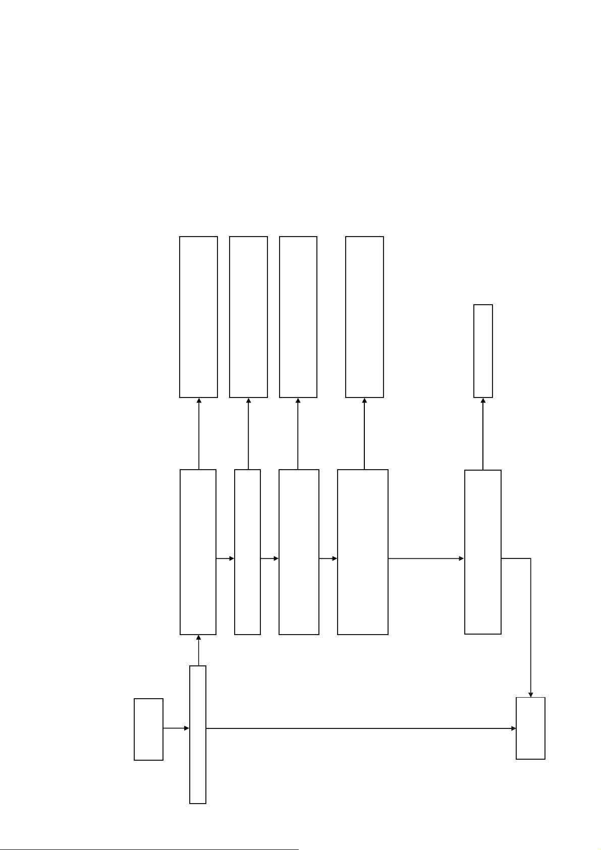
6-1. Block Diagram - CD/USB Section - ................................ 27
6-2. Block Diagram - MAIN Section - .................................... 28
6-3. Block Diagram - AMP Section - ...................................... 29
6-4. Block Diagram
- PANEL/POWER SUPPLY Section - ............................. 30
6-5. Printed Wiring Board
- MB Board (Component Side) (Suffi x-11) - .................. 32
6-6. Printed Wiring Board
- MB Board (Conductor Side) (Suffi x-11) - ....................33
6-7. Printed Wiring Board
- MB Board (Component Side) (Suffi x-12) - .................. 34
6-8. Printed Wiring Board
- MB Board (Conductor Side) (Suffi x-12) - ................... 35
6-9. Schematic Diagram
- MB Board (1/6) (Suffi x-11/-12) - ................................. 36
6-10. Schematic Diagram
- MB Board (2/6) (Suffi x-11/-12) - ................................. 37
6-11. Schematic Diagram
- MB Board (3/6) (Suffi x-11/-12) - ................................. 38
6-12. Schematic Diagram
- MB Board (4/6) (Suffi x-11/-12) - ................................. 39
6-13. Schematic Diagram
- MB Board (5/6) (Suffi x-11/-12) - ................................. 40
6-14. Schematic Diagram
- MB Board (6/6) (Suffi x-11/-12) - ................................. 41
6-15. Printed Wiring Board - PANEL Board - ......................... 42
6-16. Schematic Diagram - PANEL Board (1/2) - ...................43
6-17. Schematic Diagram - PANEL Board (2/2) - ...................44
6-18. Printed Wiring Board
- SMPS-300W Board (ESX6) - ....................................... 45
6-19. Schematic Diagram
- SMPS-300W Board (ESX6) - ....................................... 46
6-20. Printed Wiring Board
- SMPS-400W Board (ESX8) - ....................................... 47
6-21. Schematic Diagram
- SMPS-400W Board (ESX8) - ....................................... 48
6-22. Printed Wiring Board
- SMPS-600W Board (ESX9) - ....................................... 49
6-23. Schematic Diagram
- SMPS-600W Board (ESX9) - ....................................... 50
6-24. Printed Wiring Board - REGULATOR Board - ............... 51
6-25. Schematic Diagram - REGULATOR Board - .................. 51
7. EXPLODED VIEWS
7-1. Case Section ..................................................................... 66
7-2. Back Panel Section ..........................................................67
7-3. Front Panel Section .......................................................... 68
7-4. Chassis Section ................................................................ 69
7-5. CD Mechanism Section
(CDM90-DVBU202//C) .................................................. 70
8. ELECTRICAL PARTS LIST
................................ 71
3

HCD-ESX6/ESX8/ESX9
Ver. 1.1
SECTION 1
SERVICING NOTES
NOTES ON HANDLING THE OPTICAL PICK-UP
BLOCK OR BASE UNIT
The laser diode in the optical pick-up block may suffer electrostatic break-down because of the potential difference generated by
the charged electrostatic load, etc. on clothing and the human body .
During repair, pay attention to electrostatic break-down and also
use the procedure in the printed matter which is included in the
repair parts.
The fl exible board is easily damaged and should be handled with
care.
NOTES ON LASER DIODE EMISSION CHECK
The laser beam on this model is concentrated so as to be focused
on the disc refl ective surface by the objective lens in the optical
pick-up block. Therefore, when checking the laser diode emission,
observe from more than 30 cm away from the objective lens.
UNLEADED SOLDER
Boards requiring use of unleaded solder are printed with the leadfree mark (LF) indicating the solder contains no lead.
(Caution: Some printed circuit boards may not come printed with
the lead free mark due to their particular size)
: LEAD FREE MARK
Unleaded solder has the following characteristics.
• Unleaded solder melts at a temperature about 40 °C higher
than ordinary solder.
Ordinary soldering irons can be used but the iron tip has to be
applied to the solder joint for a slightly longer time.
Soldering irons using a temperature regulator should be set to
about 350 °C.
Caution: The printed pattern (copper foil) may peel away if
the heated tip is applied for too long, so be careful!
• Strong viscosity
Unleaded solder is more viscous (sticky, less prone to fl ow)
than ordinary solder so use caution not to let solder bridges
occur such as on IC pins, etc.
• Usable with ordinary solder
It is best to use only unleaded solder but unleaded solder may
also be added to ordinary solder.
NOTE OF REPLACING THE IC501, IC502, IC504 AND
IC851 ON THE MB BOARD
IC501, IC502, IC504 and IC851 on the MB board cannot exchange
with single. When these parts on the MB board are damaged,
exchange the entire mounted board.
MODEL IDENTIFICATION
– Model Number Label –
Parts No.
Model Part No.
ESX6
ESX8
ESX9: E93
ESX9: E2, E51, MX
4-460-373-0[]
4-460-373-1[]
4-460-373-2[]
4-460-373-3[]
• Abbreviation
E2 : 120 V AC area in E model
E4 : African model
E51 : Chilean and Peruvian models
E93 : 240 V AC area in E model
MX : Mexican model
MB BOARD DISCRIMINATION
In this set, the MB board has been changed in the midway of
production.
When MB board (Suffi x-11) is damaged, exchange to the MB
board (Suffi x-12).
– MB Board (Component Side) –
RELEASING THE DISC TRAY LOCK
The disc tray lock function for the antitheft of an demonstration
disc in the store is equipped.
Releasing Procedure:
1. Press the [
] button to turn the power on.
?/1
2. Press the [FUNCTION] button to select CD function.
3. Press the [x] and [REC TO USB] button simultaneously and
hold down for around 5 seconds.
4. The message “UNLOCKED” is displayed and the disc tray is
unlocked.
Note: When “LOCKED” is displayed, the slot lock is not released by turn-
ing power on/off with the [
?/1
] button.
4
SUFFIX-11 : 1-887-382-11
SUFFIX-12 : 1-887-382-12

SERVICE POSITION OF CDM90-DVBU202//C
d
HCD-ESX6/ESX8/ESX9
SERVICE POSITION OF BOARDS
MS-476 board
(E93)
CD mechanism
(CDM90-DVBU202//C)
stand
SMPS-300W board (ESX6)
SMPS-400W board (ESX8)
SMPS-600W board (ESX9)
PANEL board
MB board
REGULATOR boar
5

HCD-ESX6/ESX8/ESX9
HOW TO OPEN THE TRAY WHEN POWER SWITCH TURN OFF
Note 1: After the side panel (L, R) and top panel is removed, this word is done.
Note 2: Please prepare the thin wire (clip etc. processed to the length of 8 cm or more).
1 Remove the side case (L, R) and top case.
(Illustration of disassembly is omitted.)
tray
– Side view –
hole
Insert the clip etc.
processed to the
length of 8 cm or
more in the hole
on the side of the
chassis and push.
8 cm or more
Push after it inserts it in this hole well.
Note:
CD drive
2 Insert the clip etc.
tray
– Top view –
CAPACITOR DISCHARGE FOR ELECTRIC SHOCK PREVENTION
SMPS-300W BOARD (Conductor side view)
In checking the SMPS-300W board, make 3 capacitors discharge of C914, C1003 and C1004 for electrical shock prevention.
3
800 :/5 W 800 :/5 W
C914
C1004
C1003
800 :/5 W
6

HCD-ESX6/ESX8/ESX9
SMPS-400W BOARD (Conductor side view)
In checking the SMPS-400W board, make 2 capacitors discharge of C914 and C1012 for electrical shock prevention.
800 :/5 W
C914
C1012
800 :/5 W
SMPS-600W BOARD (Conductor side view)
In checking the SMPS-600W board, make 3 capacitors discharge of C914, C1000 and C1006 for electrical shock prevention.
800 :/5 W
C914
800 :/5 W
C1006
C1000
800 :/5 W
7

HCD-ESX6/ESX8/ESX9
PRECAUTION WHEN INSTALLING A NEW OP UNIT/
PRECAUTION BEFORE UNSOLDERING THE STATIC
ELECTRICITY PREVENTION SOLDER BRIDGE
(CDM90-DVBU202//C)
When installing a new OP unit, be sure to connect the fl exible
printed circuit board fi rst of all before removing the static electric-
ity prevention solder bridge by unsoldering.
Remove the static electricity prevention solder bridge by unsoldering after the fl exible printed circuit board has already been con-
nected.
(Do not remove nor unsolder the solder bridge as long as the OP
unit is kept standalone.)
8

DISASSEMBLY
• This set can be disassembled in the order shown below.
2-1. DISASSEMBLY FLOW
SET
2-2. SIDE CASE (L), SIDE CASE (R),
TOP CASE
(Page 10)
2-3. LOADING PANEL
(Page 10)
2-4. CD MECHANISM SECTION
(CDM90-DVBU202//C)
(Page 11)
HCD-ESX6/ESX8/ESX9
SECTION 2
2-5. FRONT PANEL SECTION
(Page 11)
2-6. MB BOARD
(Page 12)
2-7. SMPS-300W BOARD (ESX6), SMPS-400W BOARD (ESX8),
SMPS-600W BOARD (ESX9)
(Page 12)
2-8. SERVICE OPTICAL DEVICE,
WIRE (FLAT TYPE)
(Page 13)
9
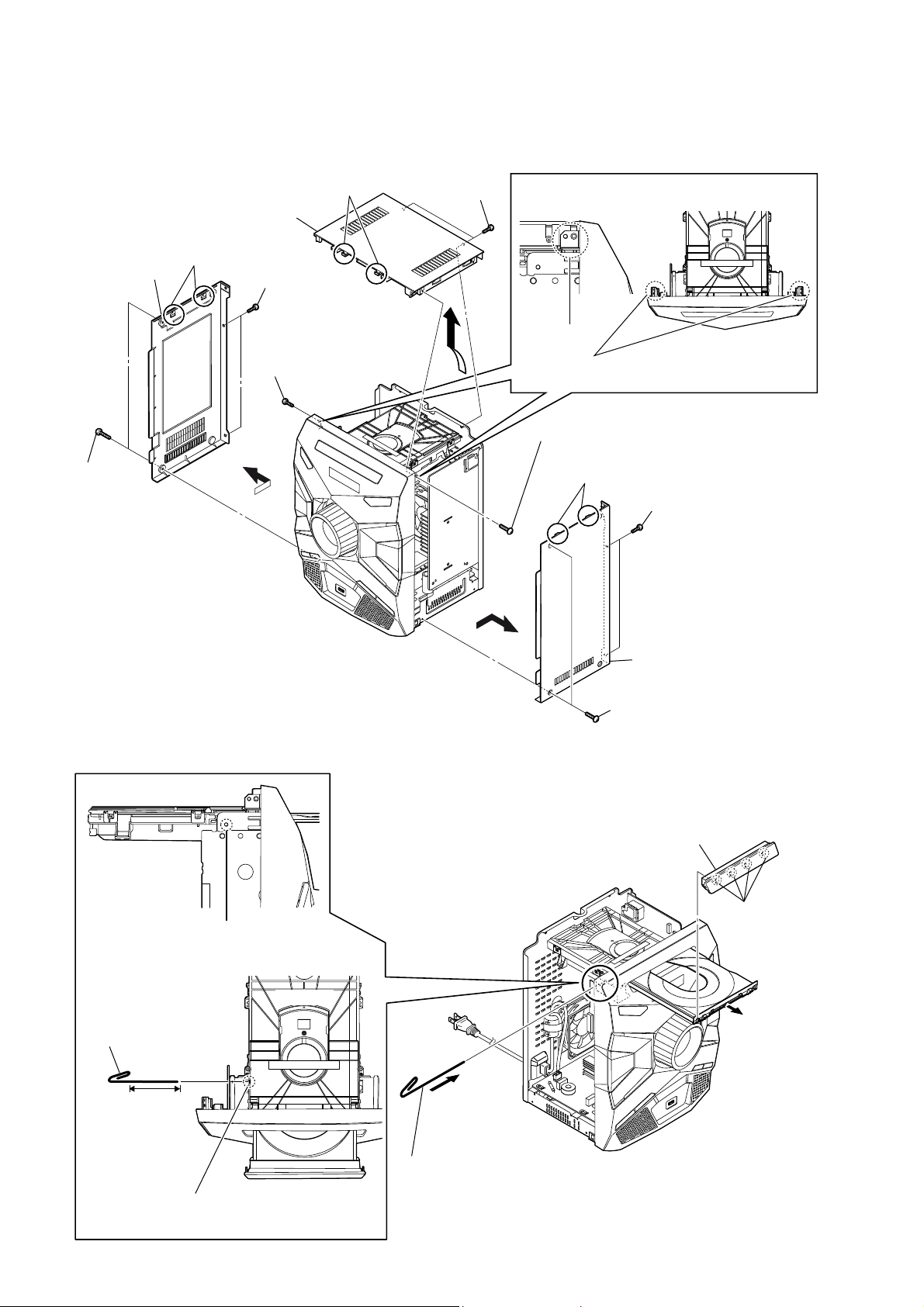
HCD-ESX6/ESX8/ESX9
s
Note: Follow the disassembly procedure in the numerical order given.
2-2. SIDE CASE (L), SIDE CASE (R), TOP CASE
5 case (L), side
1 two screws
(CASE 3 TP2)
qj case, top
4 two claws
3
qh two hooks
2 two screws
(+BVTP 3 u8)
qa one screw
(+BVTP 3 u8)
qd two screws
(+BVTP 3 u8)
qg
qf
– Side view –
hook
Pull the hook outwards to release the groove.
Note:
Then, release the case, top.
qs one screw
(+BVTP 3 u8)
9 two claws
– Top view –
7 two screws
(+BVTP 3 u8)
2-3. LOADING PANEL
– Side view –
Insert the clip etc.
processed to the
length of 8 cm or
more in the hole
on the side of the
chassis and push.
8
0 case (R), side
6 two screws
(CASE 3 TP2)
4 panel, loading assy
3 four claw
hole
CD drive
2
10
8 cm or more
Push after it inserts it in this hole well.
Note:
tray
1 Insert the clip etc.
– Top view –

2-4. CD MECHANISM SECTION (CDM90-DVBU202//C)
8 CD mechanism section
7 two screws
(+BVTP 3 u8)
(CDM90-DVBU202//C)
HCD-ESX6/ESX8/ESX9
Ver. 1.1
6 one screw
(+BVTP 3 u8)
qd one screw
(+BVTP 3 u8)
(E93)
qa cushion (H)
qf REGULATOR board
0 CDM metal, L
qs CN2000 (10P)
9 two screws
(+BVTP 3 u8)
(E93)
1 wire (flat type)
(5 core) (CN681)
2 wire (flat type)
(24 core) (CN801)
(E93)
3 tape
5 CN831 (7P)
0 CDM metal, R
(E93)
4 cushion (E 0.5)
2-5. FRONT PANEL SECTION
7 front panel section
4 wire (flat type)
(21 core) (CN300)
2 wire (flat type)
(23 core) (CN301)
5 three screws
(+BVTP 3 u8)
1 CN802 (3P)
6 claw
6 claw
3 wire (flat type)
(13 core) (CN2004)
(ESX6/ESX8)
3 wire (flat type)
(13 core) (CN2004)
(ESX9)
11
HCD-ESX6/ESX8/ESX9
Ver. 1.1
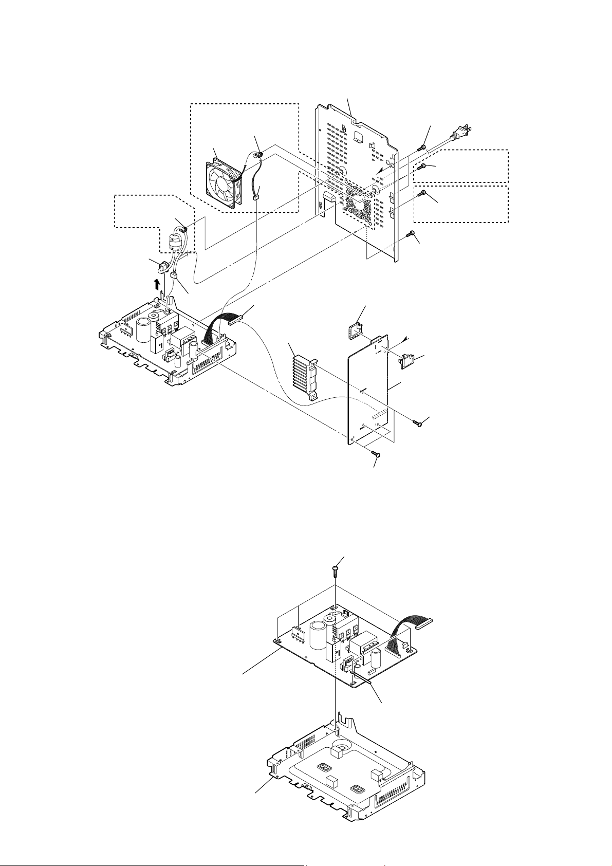
2-6. MB BOARD
8 panel, back
(ESX9: E93)
qs holder, wire
qa bushing (2104), cord
0
(ESX8/ESX9)
7 DC fan
9 CN901
(2P)
5 holder, wire
4 CN2000
(3P)
qd CN1700 (12P)
qh heat sink (DAMP)
2 two screws
(+BVTP 3 u 8)
B
qj tuner, top
(ESX8/ESX9)
6 two screws
(+BVTP 3 u 8)
(ESX9)
3 one screw
(+BVTP 3 u 8)
1 one screw
(+BVTP 3 u 8)
B
qk tuner, bottom
ql MB board
qg two screws
(+BVTP 3 u 8)
qf two screws
(+BVTP 3 u 8)
2-7. SMPS-300W BOARD (ESX6), SMPS-400W BOARD (ESX8), SMPS-600W BOARD (ESX9)
1 five screws
(+BVTP 3 u8)
3 SMPS-300W board (ESX6)
SMPS-400W board (ESX8)
SMPS-600W board (ESX9)
2 clip, coating
12
4 chassis
HCD-ESX6/ESX8/ESX9
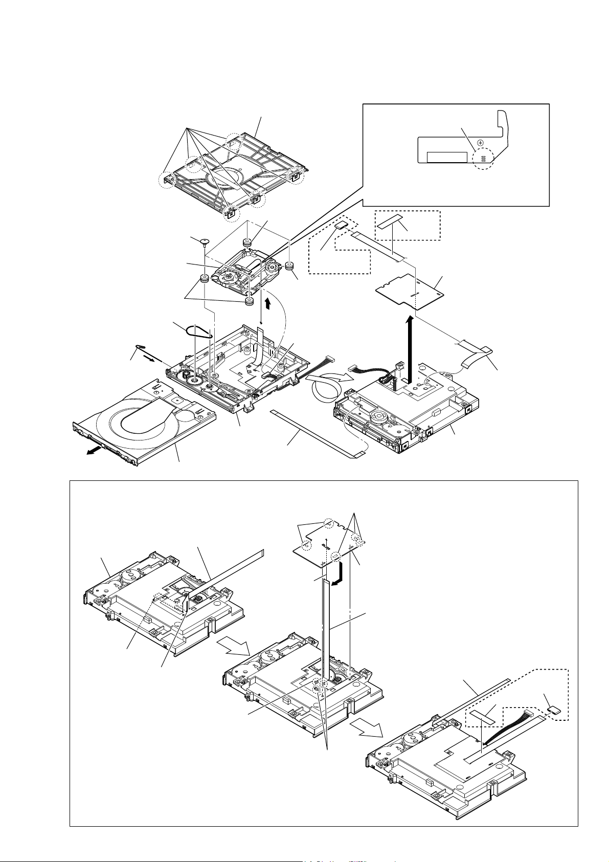
2-8. SERVICE OPTICAL DEVICE, WIRE (FLAT TYPE)
Note 1 : Before disconnecting the wire (fl at type) (24 core) of optical pick-up block, solder the short-land.
8 four insulator screws
qs service,
optical device
3 Insert the thin
wire (clip etc.).
1 six claws
qa insulator
6 belt
2 chuck holder assy (MB)
qa insulator
qj core, ferrite
qa insulator
0
9
7 connector
2 Solder the short-land.
Note 2: When assembling the optical pick-up block,
remove the solder of short-land after
connecting the wire (flat type) (24 core).
(E93)
qh tape
(E93)
qg
qk holder, FFC
ql wire (flat type)
(24 core)
qd loading base
4
5 tray
,QVWDOODWLRQRIZLUHIODWW\SHFRUHDQGZLUHIODWW\SHFRUH
This illustration sees the loading assy (MB) from bottom side.
Note:
1 wire (flat type) (24 core)
loading assy (MB)
terminal face
2 Through the hole
assy
qf wire (flat type)
(5 core)
5 two claws
3 Through the hole
Under the guide
(Fold area)
5 three claws
6 holder, FFC
4
– Bottom view –
7 wire (flat type)
(24 core)
loading assy (MB)
0 wire (flat type)
(5 core)
(
8 core, ferrite
9 tape
Under the guide
13

HCD-ESX6/ESX8/ESX9
SECTION 3
ESX TEST MODE
[PANEL TEST MODE]
• This mode is used t o check the l iquid cr ys tal d isplay, LEDs,
keys, [VOLUME] jog, model, destination and software
version.
Procedure:
1. Press [FUNCTION] button and [BASS BAZUCA] button
simultaneously and hold 3 seconds.
2. All LEDs and segments of liquid crystal display will light up.
3. In the Panel Test Mode, when you want to enter to the
software version display mode, press [+] button. The model
information appears on the fl uorescent indicator tube.
• “ESX0” is shown for MHC-ESX6.
• “ESX1” is shown for MHC-ESX8.
• “ESX2” is shown for MHC-ESX9.
Press [+] button again to view the destination information.
4. During the destination information display, press [+]
button. Each time [+] button is pressed, the fl uorescent
indicator t ube shows the version of each categor y software
in the following sequence: SC, MTK, OPU , UI, PF, SYS, CD,
CMA, CM B, ST, TA, TAS, TM and ret urn back to model
information display.
5. When [FUNCTION] button is pressed while the version
numbers a re being displayed except mo del and destinat ion,
the date of the software creation appears. When [FUNCTION]
button is pre ssed again, t he display retur ns to the soft ware
version display.
Press [–] button, the key check mode is activated.
6.
7. In the key check mode, the liquid crystal display will displays
“K 0 V0”.
Each time a button is pressed, “K” value increases. However,
once a button has been pressed, it is no longer taken into
account.
“V” value increases in the manner of 0, 1, 2, 3 ... if [MASTER
VOLUME] knob is turned clockwise, or it decreases in the
manner of 0, 9, 8, 7 ... if [MASTER VOLUME] knob is turned
counterclockwise.
8. When [ ] button is pres sed af t er al l LEDs a nd seg ment s in
liquid cr ystal display light u p, alter nate segments in l iquid
cryst al display and LEDs would l ight up. If you press [ ]
button again, another half of alternate segments in liquid
crystal display and LEDs would light up. Pressing [ ] button
again would cau se all s egment s in l iquid cr yst al d isplay and
LEDs light up. Pre ssi ng [ ] button aga in would t u rn off all
segments in fl uorescent indicator tube and all LEDs.
9. To release from this mode, press the buttons in the same
manner as step 1, or disconnect the power cord.
[USER RESET]
• The user reset clears a ll data i ncluding p reset dat a stored i n
the data fl ash to initial conditions exclude history mode data.
Procedure:
1. Press [&/1] button to turn on the system.
2. Press [FUNCTION] button and [&/1] button simultaneously
for 3 seconds.
3. “R ESET” appears on the liquid cryst al display. Afte r that,
the liquid c r yst al d isplay bec omes bla nk for a wh ile, a nd the
system is reset.
[CD SHIP MODE (WITH MEMORY CLEAR)]
• This mode moves the optica l pick-up to the position du rable
to vibration and clears all data including preset data stored in
the data fl ash to initial conditions during the next AC-In. Use
this mode when returning the set to the customer after repair.
Procedure:
1. Press [\/1] button to turn on the system.
2. Press [FUNCTION] button to select CD function.
3.
Press [OPTIONS] button and [TUNING –] button simultaneously
for 3 seconds. The system turns off automatically.
4. A message “MECHA LOCK” is displayed on the liquid
crystal display and the CD ship mode is set.
[CD TRAY LOCK MODE]
• This mode let you lock the disc tray. When this mode is
activated, the disc tray will not open when [Z] button is
pressed. T he message “LOCK ED” will be d isplayed on the
liquid cr ysta l display. This mode only a pplied when the re is
disc(s) on the tray.
Procedure:
1. Press [\/1] button to turn on the system.
2. Press [FUNCTION] button to select CD function.
3. Press [ ] button and [REC TO USB] button simultaneously
and hold down until “LOCKED” or “UNLOCKED” displayed
on the liquid crystal display (around 5 seconds).
[CDM AGING MODE]
• This mode is used for CDM aging.
Procedure:
1. Press [\/1] button to turn on the system.
2. Press [FUNCTION] button to select CD function.
3. Open the disc tray, insert a disc and close the tray.
4. Press [REC TO USB ] button and [EQ +] button simultaneously
for 3 seconds.
5. The liquid crystal display displays Aging Display
“xxxxyyyy”.
“xxxx” represents the error counter
(Maximum Value of “xxxx” = 9999)
“yyyy” represents the cycle counter
(Maximum Value of “yyyy” = 9999)
6. Press [
The liquid crystal display displays “Mx” for 2 seconds to
x: error history number
E1: Loading sequence JCP high
E2: Loading sequence JCP low
E3: Loading operation JCP
E4: Cam position operation JCP
7. Press [ ] to Aging Display
• To release from CDM Aging Mode.
To release from this mode, pres s [\/1] button or perform COLD
RESET operation.
TUNING + M >]
search for Aging History Error Display.
indicate selected history number. Then, liquid crystal display
displays “E1E2E3E4”.
or [TUNING – .m
] to
[COLD RESET]
• The cold reset clears all d ata includ ing pres et data s tored in
the data fl ash to initial conditions included history mode data.
Execute this mode when returning the set to the customer.
Procedure:
1. Press [&/1] button to turn on the system.
2. Press [ENTER] button and [&/1] button simultaneously for 3
seconds.
3. “COLD RST” appears on the liquid crystal display. After
that, the liquid crystal display becomes blank for a while, and
the system is reset.
14
[HISTORY MODE]
• This mode is used to check important data stored in the system
when PROTECTOR happen.
Procedure:
u
1. During demo mode, press [
seconds to mode in to history mode.
Press the [TUNING + M >] or
2.
button to check history data stored
Display on liquid crystal display Description
PCOUNT
PT
※※※※
] button and [ENTER] for 5
[TUNING – .m]
.
※※
No of time protector happen (0 ~ 99)
Indication protector type (refer protector kind test mode)
Protector type Protector Error Code
AMP E03
DC E04
FAN E06
HCD-ESX6/ESX8/ESX9
1 *h*h*h*h*h*m*m
2 *h*h*h*h*h*m*m
F
VOL
ATT
LOW
MID
HIGH
VACS
APVACS
SURR
BASS
• To release from History Mode.
To release from this mode, press [\/1] button.
[PROTECT KIND CHECK TEST MODE]
• This mode is use d to check t y pe s of protect o ccu r re d du ri ng
protector on.
Procedure:
1. Dur ing protect ion on, liquid cr ystal display shows blin king
message “PROTECT EXX” where “EXX” represent the error
code.
2. Press [
3. Liquid crystal display will toggle between “PROTECT”
message and protector kind message display.
Below table explains on protector kind.
※※※※※※
※※※
※※※
※※※
※※※
※※※
※※※
※※※
u
] button and [OPTIONS] button simultaneously.
Single Power On Time until protector happened
(0~99999 hours, 0~99Min)
Total Power On Time [ no consider protector happen ]
(0~99999 hours, 0~99Min)
Input Function during protector happened
Volume setting (MIN / 1 - 50 / MAX)
Actual attenuation (-87 … 0)
Low EQ level (-6 … 0 … +6)
Mid EQ level (-6 … 0 … +6)
High EQ level (-6 … 0 … +6)
VACS level (0 ... 5)
※
AP VACS level (0 … 7)
※
Surround setting (OFF / ON)
Bass Bazuca setting (OFF / ON)
Error
Code
E03 “AMP ERR” Amplifi er Defect
E04 “DC DET” DC different appears in
E06 “FANBLOCK” Defect of DC FAN and DC
• To release from this mode:
Press [
Protector Message Description
SPEAKER terminal due to
Amplifi er defect.
FAN driver circuit
u
] button and [OPTIONS] button simultaneously
again or unplug and re-plug in the power cord.
15

HCD-ESX6/ESX8/ESX9
SECTION 4
ELECTRICAL CHECK
CD SECTION
Note:
1. CD Block is basically constructed to operate without adjustment.
2. Use YEDS-18 disc (Part No. 3-702-101-01) unless otherwise indicated.
3. Use an oscilloscope with more than 10 MΩ impedance.
4. Clean the object lens by an applicator with neutral detergent when the
signal level is low than specifi ed value with the following checks.
5. Check the focus bias check when optical pick-up block is replaced.
FOCUS BIAS CHECK
oscilloscope
(DC range)
MB board
CN507 pin 6 (RFMON)
CN507 pin 3 (GND)
+
–
Procedure :
1. Connect the oscilloscope to CN507 pin 6 (RFMON) and
CN507 pin 3 (GND) on the MB board.
2. Press the [
] button to turn the power on, and press the
?/1
[FUNCTION] button to select CD function.
3. Set disc (YEDS-18) and press the [u] button to playback.
4. Confi rm that oscilloscope waveform is as shown in the fi gure
below (eye pattern).
A good eye pattern means that the diamond shape () in the
center of the waveform can be clearly distinguished.
VOLT/DIV: 200 mV
TIME/DIV: 500 ns
level:
1.0 ± 0.25 Vp-p (CD)
TUNER SECTION
0 dB = 1 V
FM AUTO STOP CHECK
signal
generator
set
+
75 :
–
Procedure:
1. Turn the power on.
2. Input the following signal from Signal Generator to FM antenna input directly.
Carrier frequency : A = 87.5 MHz, B = 98 MHz, C = 108 MHz
Deviation : 75 kHz
Modulation : 1 kHz
ANT input : 35 dBu (EMF)
Note: Please use 75 ohm “coaxial cable” to connect SG and the set. You
cannot use video cable for checking.
Please use SG whose output impedance is 75 ohm.
3. Set to FM tuner function and scan the input FM signal with
automatic scanning.
4. Confi rm that input Frequency of A, B and C detected and auto-
matic scanning stops.
The stop of automatic scanning means “The station signal is received in good condition”.
Checking Location:
-MB Board (Component Side)-
pin 3 (GND)
CN507
pin 6 (RFMON)
16

SECTION 5
TROUBLESHOOTING
HCD-ESX6/ESX8/ESX9
1. AC Input CN901
No. Desc Ref No.
2. 6.3A/250V AC Fuse F901
3. Retifi er - KBJ1006G D902
4. 0.1Ω Fuse Resistor R914
(11)
5. A931 Main Primary Heat Sink ASSY A931
6. Main Transformer T901
(9)
pin 1 to 5: V1 output (36V±1.8V)
pin 6 to 9: V1 GND
pin 10: DCDC 12.5V
pin 11: DCDC 12.5V GND
7. A932 Main Secondary Diode Heat Sink A932
8. CN4 connector CN4
(8)
(10)
(5)
pin 12: No Connect
pin 13: Fan Speed
pin 1: Thermal VACS cct 3.3V
pin 2: Thermal DET
9. CN2004 connector CN2004
(7)
(6)
pin 3: 3.3V GND
pin 4: ECO Ever 7V/12V
pin 5 to 6: DCDC 12.5V
pin 7 to 8: DCDC 12.5V GND
pin 9: Fan supply (DCDC 5.1V)
pin 10: Main On
pin 11: Fan block
pin 12: No Connect
pin 13: Fan Drive
(4)
11. JW958 for V1 GND (-)
10. JS1002 for V1 ouput (+)
(1)
(2)
(ESX6)
Switching Regulator (AMP-SMPS) Diagnosis Flow (1/4)
(3)
17

HCD-ESX6/ESX8/ESX9
1. AC Input CN901
No. Desc Ref No.
2. 10A/250V AC Fuse F901
(10)
3. Retifi er - KBJ1006G D902
(12)
4. 0.1Ω Fuse Resistor R914
5. A931 Main Primary Heat Sink ASSY A931
(9)
6. Main Transformer T901
pin 1 to 5: V1 output (50V±2.5V)
pin 6 to 9: V1 GND
pin 10: DCDC 12.5V
pin 11: DCDC 12.5V GND
7. A932 Main Secondary Diode Heat Sink A932
8. CN4 connector CN4
(8)
(11)
(5)
pin 12: No Connect
pin 13: Fan Speed
pin 1: Thermal VACS cct 3.3V
pin 2: Thermal DET
9. CN2004 connector CN2004
(7)
(6)
pin 3: 3.3V GND
pin 4: ECO Ever 7V/12V
pin 5 to 6: DCDC 12.5V
pin 7 to 8: DCDC 12.5V GND
pin 9: Fan supply (DCDC 5.1V)
(4)
pin 10: Main On
pin 11: Fan block
pin 12: No Connect
pin 13: Fan Drive
11. JS1002 for V1 ouput (+)
10. Fan Connector CN2000
12. JW958 for V1 GND (-)
(1)
(2)
(ESX8)
Switching Regulator (AMP-SMPS) Diagnosis Flow (2/4)
18
(3)

HCD-ESX6/ESX8/ESX9
1. AC Input CN901
No. Desc Ref No.
2. 10A/250V AC Fuse F901
3. Retifi er - D15XB60 D902
4. 0.1Ω Fuse Resistor R914
5. A931 Main Primary Heat Sink ASSY A931
6. Main Transformer T901
(14)
7. 2.2Ω Fuse Resistor R965
(16)
8. A-933 Sub Controller STR-Y6763 IC965
(5)
9. Sub Transformer T903
(12)
10. A932 Main Secondary Diode Heat Sink A932
(6)
pin 1 to 5: V1 output (50V±2.5V)
pin 6 to 9: V1 GND
pin 10: V2 output (13.5V±0.65V)
pin 11: V2 GND
11. Sub Secondary Diode D1001
12. CN4 connector CN4
(15)
(10)
pin 12: No Connect
pin 13: Fan Speed
pin 1: Thermal VACS cct 3.3V
pin 2: Thermal DET
13. CN2004 connector CN2004
(13)
(17)
(9)
(7)
(4)
pin 3: 3.3V GND
pin 4: No Connect
pin 5 to 6: V2 output (13.5V±0.65V)
pin 7 to 8: V2 GND
pin 9: Fan supply
pin 10: Main On
pin 11: Fan block
(18)
(11)
(8)
pin 12: No Connect
pin 13: No Connect
14. Fan Connector CN2000
15. JS1002 for V1 output (+)
16. JW922 for V1 GND (-)
17. JW923 for V2 output (+)
18. JS1000 for V2 output (-)
(1)
(2)
(ESX9)
Switching Regulator (AMP-SMPS) Diagnosis Flow (3/4)
(3)
19
HCD-ESX6/ESX8/ESX9
AC IN
Check whether state of cable and outlet are normal.
If there are no problem, check circumference circuit from
Main On on output of panel side
No
Hi (3.3V)
Power On
Power On
Yes
Replace SMPS parts
ESX9
Main output -> A931(Q908,Q909,D903), R914
Sub output -> A933(IC965), R965
ESX8/ESX6
Main output -> A931 -> (Q908,Q909,D901), R914
No
Power OnDemo Mode
Hi (50V±2.5V)
Low (0V)
ECO Mode
Hi (36V±1.8V)JS1002(+) + JW958(-):
Hi (36V±1.8V)
Low (7V)
Yes
END
The Power Control signal to SMPS as below voltage?
ESX9
Main on ECO Mode Demo Mode Power On
CN2004 Pin10: Low (0V) Low (0V)
ESX8
Main On ECO Mode Demo Mode
ESX6
Main On ECO Mode Demo Mode
CN2004 Pin10: Low (0V) Hi (3.3V) Hi (3.3V)
CN2004 Pin10: Low (0V) Hi (3.3V) Hi (3.3V)
Switching Regulator (AMP-SMPS) Diagnosis Flow (4/4)
20
JW923(+) + JS1000(-): Hi (13.5V±0.65V) Hi (13.5V±0.65V) Hi (13.5V±0.65V)
ESX8
Main Output ECO Mode Demo Mode Power On
The SMPS output as below voltage?
ESX9
Main Output ECO Mode Demo Mode Power On
JS1002(+) + JW922(-): Low (0V)
Sub Output
JS1002(+) + JW958(-): Low (7V) Hi (50V±2.5V) Hi (50V±2.5V)
ESX6
Main Output ECO Mode Demo Mode Power On
§9
C
§9
E
HCD-ESX6/ESX8/ESX9
Check condition of transistor Q211, V
&KHFN,&IRU9
If there is no problem, check circumference circuit of IC2000
IRU9
&KHFN,&/'2,&IRU9
No
Yes
JL510: 1.2V
Check voltage supply to MTK IC501
JL302/CL585: 3.3V
No
Checks circumference circuit for SL+/SL- of IC851.
Checks circumference circuit of IC501 FMO Signal.
No
Yes
Does it output the signal?
Checks CN831 SL+/SL- signal (JL839/JL838).
The Sled motor has a problem.
Replaces BU.
Checks circumference circuit for FCS+/FCS- of IC851.
Checks circumference circuit for SP+/SP of IC851.
Checks circumference circuit of IC501 DMO Signal.
No
Yes
The Spindle motor has a problem.
Does it output the signal?
Checks CN831 SP+/SP- signal (JL834/JL835).
No
Replaces BU.
Checks circumference circuit of IC501 FOO Signal.
No
Yes
Does it output the signal?
Checks CN801 FCS+/FCS- signal (JL823/JL824).
No
The Optical pickup has a problem.
Replaces BU.
Yes
REMOVE CDM TOP PANEL
TURN ON
REMOVE TOP P ANEL
REMOVE SIDE PANEL
Optical Block Diagnosis Flow (1/2)
TRAY IN
Does Optical pickup move to inner circumference?
(Visual check)
Yes
Does Spindle motor rotate?
(Visual check)
Yes
Does Optical pickup do focus search?
(Visual check)
A
21
HCD-ESX6/ESX8/ESX9
Checks circumference circuit of Q881 or Q891.
Checks circumference circuit of IC501 LDO1 and LDO2.
No
Yes
The Optical pickup has a problems.
Does it output 1.8V when laser become luminous ?
Check JL806 (LD780) signal.
Does it output 2.2V when laser become luminous ?
Check JL802 (LD650) signal.
No
Replaces BU.
No
Replaces BU if it is not up to standard.
No
Yes
If it is not up to standard,
Lens cleaning is performed.
Is output level of RF signal(CN507 6pin) up to standard?
RF Level = 1.0 ±0.25 Vpp
Test CD:YEDS-18
Yes
No
The Optical pickup has a problems.
Replaces BU.
A
Optical Block Diagnosis Flow (2/2)
Does laser diode become luminous ?
22
Yes
(Visual check)
Yes
DISC IN
Yes
Test CD:YEDS-18
RF Level = 1.0 ±0.25 Vpp
Is output level of RF signal (CN507 6pin) up to standard?
Yes
Is there no problem with Long term Aging Test (60min)?
Confirms that there is no sound skip.
END

HCD-ESX6/ESX8/ESX9
Check that the voltage 12V/12.5V of MB BOARD. Make
sure L1700 is 12V.
No
Yes
Check that power voltage 3.3V of MB BOARD CN300
6PIN (SD).
Is there power voltage decrease when power on time?
No
Check that DC voltage between speaker
terminal Plus and speaker terminal Minus.
䐟 MB BOARD TB1700 for ESX6/ESX8/ESX9
Between 1PIN-2PIN
Between 3PIN-4PIN
䐠㻌MB BOARD TB1702 for ESX9 only.
Between 1PIN-2PIN
Between 3PIN-4PIN
No
Check that SD slow signal.
ESX6/ESX8/ESX9
Check that power voltage 3.3V of CN300 3PIN.
POWER ON
D-AMP Mount Diagnosis Flow (1/2)
Yes
Check that there is no “PROTECT” on LCD display.
Check that power on is available if the unit is ESX6/ESX8/ESX9
A
23
HCD-ESX6/ESX8/ESX9
Check that PANEL BOARD IC001 (SYSTEM CONTROL)
38PIN (O-AMP-RST).
Check that SMPS block power supply operation.
Refer to the Troubleshooting Power Block.
Check that power voltage of MB BOARD CN1700 13PIN,
PIN1-5 (V1)
ESX8/ESX9 50V ± 2.5V
ESX6 36V ± 1.8V
No No
ESX6/ESX8/ESX9
Yes
Check that MB BOARD C1886 voltage and peripheral
circuit.
No
Yes
Check that power voltage 12V/12.5V of MB BOARD.
Normal condition is 3.3V.
No
Check that RESET power voltage 3.3V at
MB BOARD CN300 7PIN.
Yes
ESX6/ESX8
Replace AMP IC (IC1705)
ESX9
Replace AMP IC (IC1705) for 䐟
Replace AMP IC (IC1706) for 䐠
No
Yes
JL1717 and JL1727
Check that AMP IC OUT waveform at
MB BOARD
ESX6/ESX8: JL1716 and JL1724,
JL1742 and JL1745
JL1717 and JL1727
䐠㻌JL1718 and JL1721,
ESX9: 䐟㻌JL1716 and JL1724,
Are they swing?
A
D-AMP Mount Diagnosis Flow (2/2)
24
Yes
END
PLAY MUSIC
Is signal output from speakers terminal?
HCD-ESX6/ESX8/ESX9
Reinserts the cable or Exchanges.
If there are no problems, checks output of
SMPS.
Reinserts the FFC or Exchanges.
If there are no problems, checks output of
Main on output of MB Board side.
Reinserts the cable or Exchanges.
If there are no problems, checks output of
SMPS.
NoNo
output of CN1700 10pin.
Is the power voltage OK?
Checks ESX6/ESX8: 12.5V or ESX9: 13.5V
No
Yes
Checks 3V output of CN203 2pin (PVDD_ON)
Is the power voltage OK?
No
Yes
Checks ESX6: 36V or ESX8/ESX9: 50V
output of CN1700 1pin (V1).
Is the power voltage OK?
Check circumference circuit of:
ESX6/ESX8: IC1855
ESX9: IC1856
No
Yes
Check 12V/12.5V of MB at:
ESX6/ESX8: L1700, CL1725
ESX9: L1700, CL1725 and CL1726
Is the power voltage OK?
Yes
Replaces MB Board
No
Yes
Assembles into the unit again then, checks
whether there is the audio output from
MB Board.
Yes
PLAY MUSIC
MB Mount Diagnosis Flow
Yes
END
Is there audio output from MB Board?
25

HCD-ESX6/ESX8/ESX9
• Circuit Boards Location
REGULATOR board
PANEL board
SECTION 6
DIAGRAMS
MB board
SMPS-300W board (ESX6)
SMPS-400W board (ESX8)
SMPS-600W board (ESX9)
26
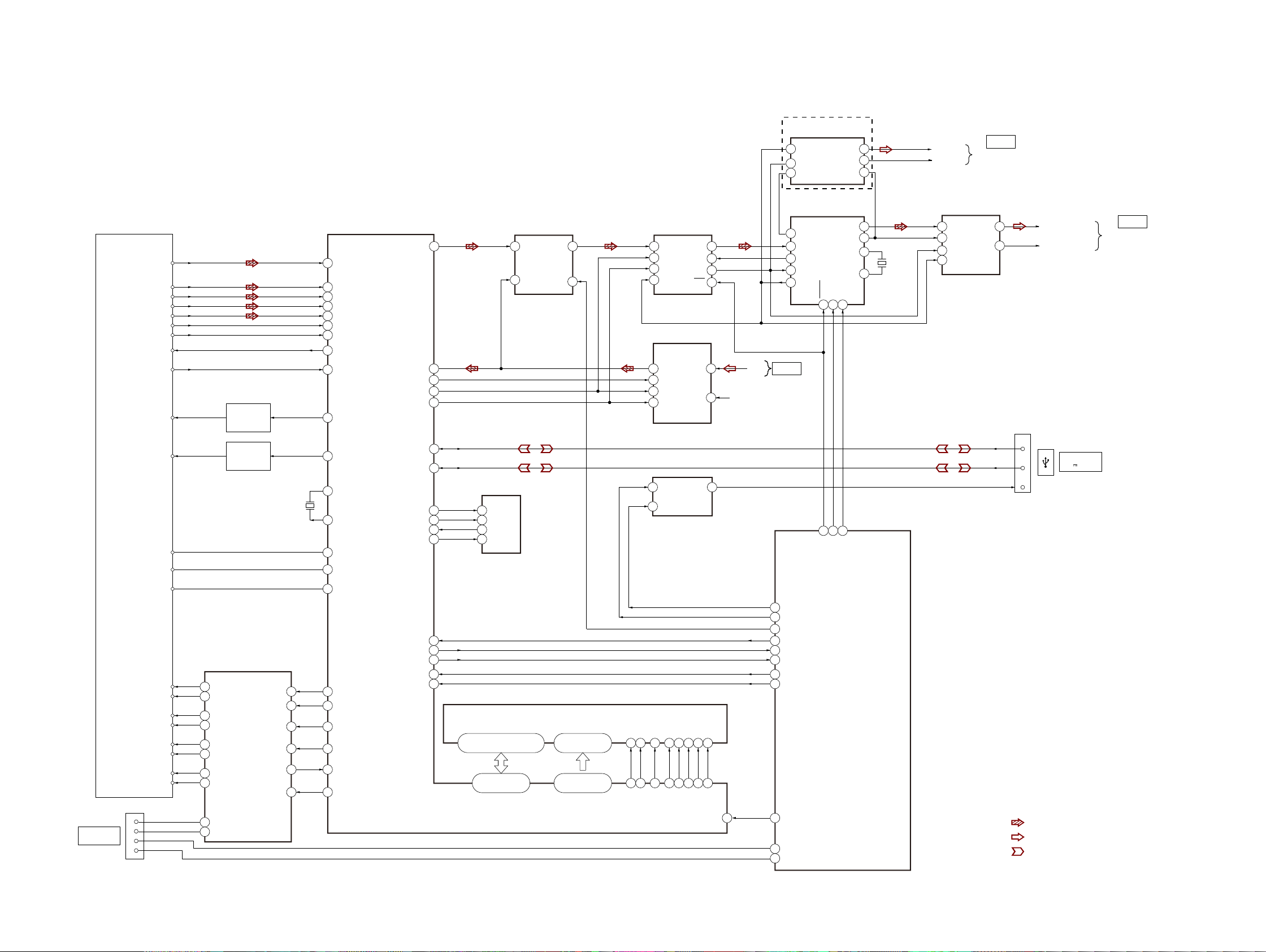
6-1. BLOCK DIAGRAM - CD/USB Section -
ESX9
STEREO D/A CONVERTER
IC751
SCK
16
3
LRCK
DATA
2
VOUTL
VOUTR
BCK
HCD-ESX6/ESX8/ESX9
7
8
1
SW OUT L
SW OUT R
>001B
AMP SECTION
(Page 29)
CONNECT TO
CDM90
VOA/A
VOB/B
VOC/C
VOD/D
SERVICE,
OPTICAL DEVICE
(LO:DVD,HI:CD)MSW
VR(780)
VR(650)
FCS+
FCS–
TRK+
TRK–
CN681
LOAD-
1
LOAD+
2
TRAY-IN
3
TRAY-OUT
5
RF
VC
PD
SL+ 17
SL– 18
SP+ 11
SP– 12
14
13
16
15
9
10
POWER CTRL
POWER CTRL
5CH SYSTEM
MOTOR DRIVER
VOFC+
VOFC-
VOTKVOTK+
VOLD+
VOLD-
VOSL+
VOSL-
VOTRVOTR+
AUTO
Q891
AUTO
Q881
IC851
VINFC
VINTK
VINLD
VINSL+
BIAS
MUTE
X501
27MHz
1
26
23
4
CD RF AMP
FOCUS/TRACKING ERROR AMP
CD SYSTEM PROCESSOR
DIGITAL SERVO PROCESSOR
IC501
123
RFIP
RF_C1
128
RF_B
127
RF_A
RF_D2
RF_F4VOE/E+G
RF_E3VOF/F+H
10
V2O
MDI1
13
LDO114LD(780)
LDO215LD(650)
XTALI7
8
XTALO
MSW23
CD_VR19
DVD_VR20
FOO22
TRO21
FMO18
DMO17
V14/VREF01127
MUTE4528
ASDATA0
ADIN
ACLK
ALRCK
ABCK
USB_DP 25
USB_DM 24
SF_CS#
SF_DO
SF_DI
SF_CK
IFSDI 40
IFSDO 35
IFSCK 34
IFCS# 42
IFBSY 41
AUDIO DSP
SDOUT2
26
SDIN1
11
22
SCLKOUT1
LRCK
19
21
MCLKO
IC701
SDOUT1
SCLKOUT2
XTALI
XTALO
SDA1
SCL1
RESET
32 15 16
24 30 29
I-DSP SCL
I-DSP SDA
O-DSP-RESET
SYSTEM CONTROL
IC001 (1/4)
27
23
3
X700
12.288MHz
4
ASYNCHRONOUS SAMPLE
SIGNAL SELECTOR
IC780
SERIAL FLASH
IC502
1
_CS
2
SO
5
SI
6
SCK
52 – 55, 57 – 60,
69 - 62
RD0 – RD15
2
B
1
A
5
Y
6
SEL
64M SDRAM
A0 – A11
23 – 26,
29 – 34, 22, 35
89 - 92, 79 - 74,
88, 73
RA0 – RA11
IC504
118
106
112
117
113
30
31
32
33
DG0, DQ1 – DQ15
2, 4, 5, 7, 8, 10, 11, 13, 42,
44, 45, 47, 48, 50, 51, 53
RATE CONVERTER
SDIN
4
LRCKI
6
BCKI
5
2
RCKI
STEREO A/D CONVERTER
9
DOUT
6
SCKI
7
LRCK
8
BCK
4
USB 5V REG.
3
20
21
38
15
85
86
72
61
BA0 BA0
BA1 BA1
RCLK CLK
IC740
IC320
IC203
39
70
DQM0 LDQM
SDOUT
LRCKO
18
83
DQM1 UDQM
BCKO
RST
VINL
VINR
17
82
RAS# RAS
23
25
24
13
13
14
16
80
CAS# CAS
PRST#
L-IN
>003B
MAIN
R-CH
6
RWE# WE
38
SECTION
(Page 28)
86
O-VBUS-OE
/I-HUB-OC-USB-A
87
O-DIGITAL-SEL
27
77
O-MTK-SDO
78
I-MTK-SDI
79
I-MTK-CLK
60
I-MTK-XIFCS
O-MTK-BUSY
66
O-MTK-RESET65
I-CDM-LOAD-SW57
I-CDM-UNLOAD-SW59
STEREO D/A CONVERTER
IC750
VOUTL
DATA
2
BCK
1
VOUTR
LRCK
3
SCK
16
VBUS
7
8
CN201
3
D+
2
D-
1
SLJQDO SDWK
: CD PLAY
: AUDIO
: USB
R-FK LV RmLWWHG GXH WR
VDmH DV L-FK.
AUDIO-OUTPUT-L
AUDIO-OUTPUT-R
DC OUT (USB)
5V 500mA
>002B
AMP SECTION
(Page 29)
HCD-ESX6/ESX8/ESX9
2727
 Loading...