

Sony HCDEP-515 Service manual
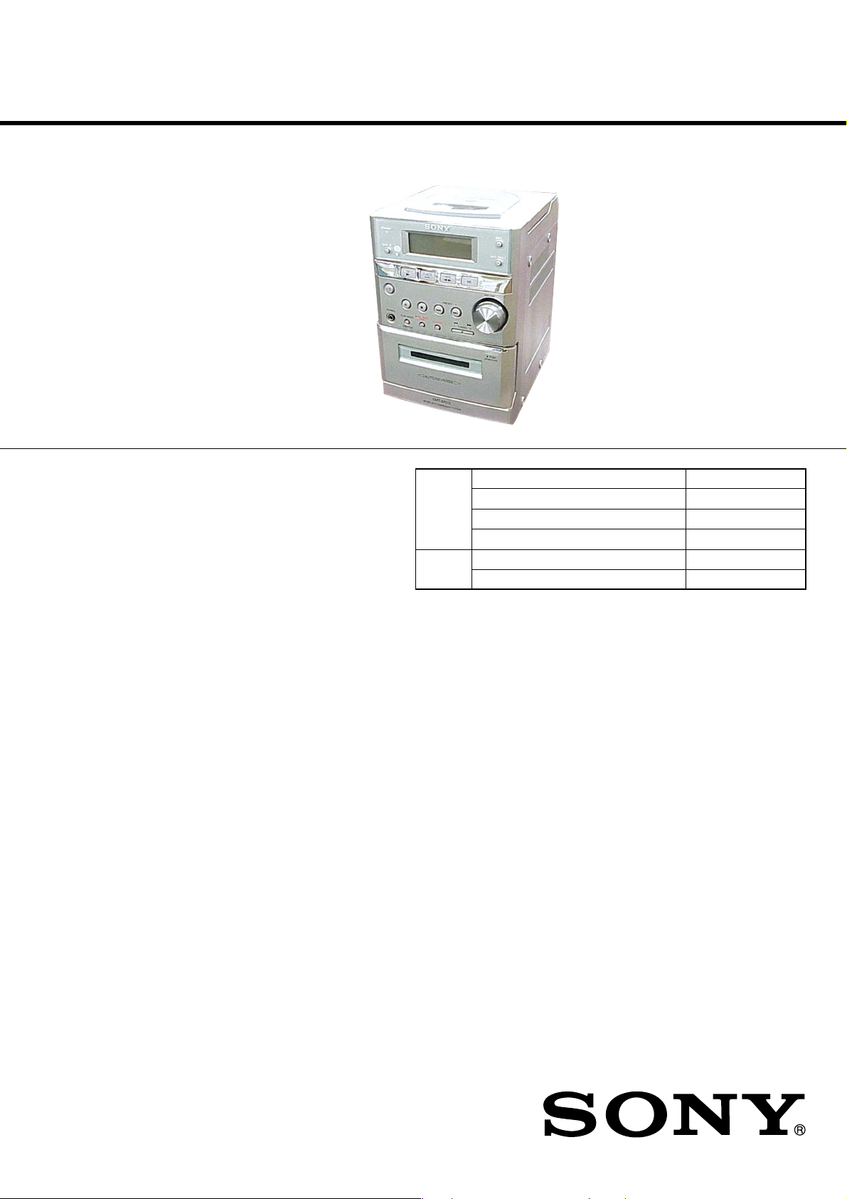
HCD-EP515
SERVICE MANUAL
Ver 1.2 2003. 07
HCD-EP515 is the Amplifier, CD player, Tape
Deck and Tuner section in CMT-EP515.
CD
Section
TAPE
Section
US Model
Canadian Model
AEP Model
UK Model
E Model
Model Name Using Similar Mechanism NEW
CD Mechanism Type KSM-213EDP
Base Unit Name BU-K7BD44B
Optical Pick-up Name KSS-213E/C2N
Model Name Using Similar Mechanism NEW
Tape Transport Mechanism Type CMAL1Z240A
Amplifier section
AUDIO POWER SPECIFICATIONS:
(U.S.A. model only)
POWER OUTPUT AND TOTAL HARMONIC
DISTORTION:
With 6-ohm loads, both channels driven, from 120 10,000 Hz; rated 14 watts per channel minimum RMS
power, with no more than 10% total harmonic
distortion from 250 milliwatts to rated output.
North American model:
Continuous RMS power output (reference):
15 + 15 W
(6 ohms at 1 kH z, 10%
THD)
European model:
DIN power output (rated): 11 + 11 W
(6 ohms at 1 kH z, DIN )
Continuous RMS power output (reference):
15 + 15 W
(6 ohms at 1 kH z, 10%
THD)
Music power output (reference ):
25 + 25 W
SPECIFICATIONS
Other models:
The following measured at AC 230 V or AC 120 V, 50/
60 Hz
DIN power output (rated): 11 + 11 W
Continuous RMS power output (reference):
Inputs
MD IN (phono jacks):
Outputs
PHONES (stereo minijack):
SPEAKER: Accepts impedance of 6 to
(6 ohms at 1 kH z, DIN )
15 + 15 W
(6 ohms at 1 kH z, 10%
THD)
Sensitivity 800 mV,
impedance 47 kilohms
Accepts headphones with
an impedance of 8 ohms or
more
16 ohms.
CD player section
System Compact disc and digital
LaserSemiconductor laser
Frequency response 2 Hz – 20 kHz (±0.5 dB)
Tape deck section
Recording sy stem 4-track 2-channel stereo
Frequency response 50 – 13,000 Hz (±3 dB),
— Continued on next page —
audio system
λ
=780 nm)
(
Emission duration:
continuous
using Sony TYPE I
cassettes
9-877-160-03
2003G16-1
© 2003.07
MICRO HI-FI COMPONENT SYSTEM
Sony Corporation
Home Audio Company
Published by Sony Engineering Corporation

HCD-EP515
Ver 1.2 2003. 07
TABLE OF CONTENTS
Tuner section
FM stereo, FM/AM superheterodyne tuner
FM tuner section
Tuning range 87.5 – 108.0 MHz (50-kHz
Antenna FM lead antenna
Antenna terminals 75 ohms balanced
Intermediate frequency 10.7 MHz
AM tuner section
Tuning range
Pan-American model: 530 – 1,710 kHz
European model: 531 – 1,602 kHz
Other models:
Antenna AM loop antenna, external
Intermediate frequency 450 kHz
General
Power requirements
North American model: 120 V AC, 60 Hz
European model: 230 V AC, 50/60 Hz
Other models: 230 V AC, 50/60 Hz
Power consumption
North American model: 50 watts
European model: 50 watts
Other models: 50 watts
Dimensions (w/h/d) Approx. 163 × 233 × 237
Mass Approx. 3.6 kg
Supplied accessories Remote (1)
step)
(with the tuning interval
set at 10 kHz)
531 – 1,602 kHz
(with the tuning interval
set at 9 kHz)
(with the tuning interval
set at 9 kHz)
530 – 1,710 kHz
(with the tuning interval
set at 10 kHz)
531 – 1,602 kHz
(with the tuning interval
set at 9 kHz)
antenna terminal
0.3 watts (in the standby
mode)
mm
R6 (size AA) batteries (2 )
AM loop antenna (1)
FM lead antenna (1)
1. SERVICING NOTES ······················································· 3
2. GENERAL ··········································································5
3. DISASSEMBLY
3-1. Rear Cabinet ··································································· 7
3-2. CD Cabinet Section, Front Panel Section ······················· 8
3-3. CD Mechanism Deck (KSM-213EDP)··························· 8
3-4. CONTROL Board, BACK LIGHT Board ······················ 9
3-5. Tape Mechanism Deck (CMAL1Z240A) ······················· 9
3-6. Cassette Door Assy ······················································· 10
3-7. POWER Board, MAIN Board ······································ 10
3-8. Optical Pick-up (KSS-213E/C2N) ································ 11
4. MECHANICAL ADJUSTMENTS ····························· 12
5. ELECTRICAL ADJUSTMENTS ······························· 13
6. DIAGRAMS······································································ 15
6-1. Block Diagram – CD Section – ··································· 17
6-2. Block Diagram – Main Section – ································ 18
6-3. Printed Wiring Board – CD Section – ························· 19
6-4. Schematic Diagram – CD Section – ···························· 20
6-5. Printed Wiring Borads – Main Section – ····················· 21
6-6. Schematic Diagram – Main Section – ························· 22
6-7. Printed Wiring Board – Control Section – ··················· 23
6-8. Schematic Diagram – Control Section –······················ 24
6-9. Printed Wiring Board – Power Section – ····················· 25
6-10. Schematic Diagram – Power Section –······················ 25
6-11. IC Pin Function Description ······································· 28
7. EXPLODED VIEWS
7-1. Cabinet Section ····························································· 30
7-2. Front Panel Section ······················································· 31
7-3. CD Cabinet Section ······················································ 32
7-4. Optical Pick-up Block (KSM-213EDP) ······················· 33
8. ELECTRICAL PARTS LIST······································· 34
Design and specifications are subject to change
without notice.
2
SECTION 1
r
SER VICING NOTES
HCD-EP515
Notes on chip component replacement
•Never reuse a disconnected chip component.
• Notice that the minus side of a tantalum capacitor may be damaged by heat.
Flexible Circuit Board Repairing
•Keep the temperature of the soldering iron around 270 ˚C during
repairing.
• Do not touch the soldering iron on the same conductor of the
circuit board (within 3 times).
• Be careful not to apply force on the conductor when soldering or
unsoldering.
SAFETY CHECK-OUT
After correcting the original service problem, perform the following
safety check before releasing the set to the customer:
Check the antenna terminals, metal trim, “metallized” knobs, screws,
and all other exposed metal parts for AC leakage.
Check leakage as described below.
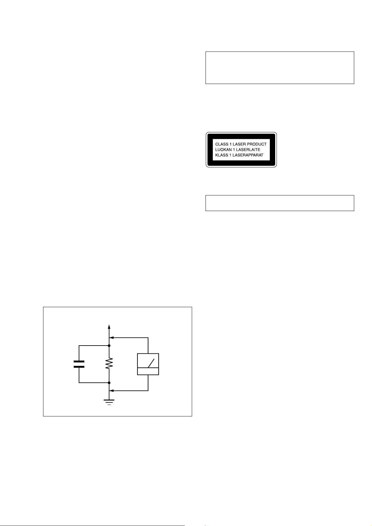
LEAKAGE TEST
The AC leakage from any exposed metal part to earth ground and
from all exposed metal parts to any exposed metal part having a
return to chassis, must not exceed 0.5 mA (500 microamperes.).
Leakage current can be measured by any one of three methods.
1. A commercial leakage tester , such as the Simpson 229 or RCA
WT-540A. Follow the manufacturers’ instructions to use these
instruments.
2. A battery-operated AC milliammeter. The Data Precision 245
digital multimeter is suitable for this job.
3. Measuring the voltage drop across a resistor by means of a V OM
or battery-operated A C voltmeter . The “limit” indication is 0.75
V, so analog meters must have an accurate low-voltage scale.
The Simpson 250 and Sanwa SH-63Trd are examples of a
passive VOM that is suitable. Nearly all battery operated digital
multimeters that have a 2 V A C range are suitable. (See Fig. A)
To Exposed Metal
Parts on Set
CAUTION
Use of controls or adjustments or performance of procedures
other than those specified herein may result in hazardous
radiation exposure.
This appliance is classified as a CLASS 1 LASER product.
The CLASS 1 LASER PRODUCT MARKING is located on
the exterior.
Laser component in this product is capable of emitting radiation
exceeding the limit for Class 1.
NOTES ON HANDLING THE OPTICAL PICK-UP
BLOCK OR BASE UNIT
The laser diode in the optical pick-up block may suffer electrostatic
break-down because of the potential difference generated by the
charged electrostatic load, etc. on clothing and the human body.
During repair, pay attention to electrostatic break-down and also
use the procedure in the printed matter which is included in the
repair parts.
The flexible board is easily damaged and should be handled with
care.
NOTES ON LASER DIODE EMISSION CHECK
The laser beam on this model is concentrated so as to be focused on
the disc reflective surface by the objective lens in the optical pickup block. Therefore, when checking the laser diode emission,
observe from more than 30 cm away from the objective lens.
LASER DIODE AND FOCUS SEARCH OPERATION
CHECK
Carry out the “S curve check” in “CD section adjustment” and check
that the S curve waveforms is output three times.
AC
1.5 k
0.15 µF
Fig. A. Using an AC voltmeter to check AC leakage.
SAFETY-RELATED COMPONENT WARNING!!
COMPONENTS IDENTIFIED BY MARK 0 OR DOTTED LINE WITH
MARK 0 ON THE SCHEMATIC DIAGRAMS AND IN THE PARTS
LIST ARE CRITICAL TO SAFE OPERATION. REPLACE THESE
COMPONENTS WITH SONY PARTS WHOSE PART NUMBERS
APPEAR AS SHOWN IN THIS MANUAL OR IN SUPPLEMENTS
PUBLISHED BY SONY .
Ω
Earth Ground
voltmete
(0.75 V)
ATTENTION AU COMPOSANT AYANT RAPPORT
À LA SÉCURITÉ!
LES COMPOSANTS IDENTIFÉS P AR UNE MARQUE 0 SUR LES
DIAGRAMMES SCHÉMA TIQUES ET LA LISTE DES PIÈCES SONT
CRITIQUES POUR LA SÉCURITÉ DE FONCTIONNEMENT. NE
REMPLACER CES COMPOSANTS QUE PAR DES PIÈSES SONY
DONT LES NUMÉROS SONT DONNÉS DANS CE MANUEL OU
DANS LES SUPPÉMENTS PUBLIÉS PAR SONY.
3
HCD-EP515
Service Position of the CD Mechanism Deck
Service Position of the Tape Cassette Mechanism Deck
4
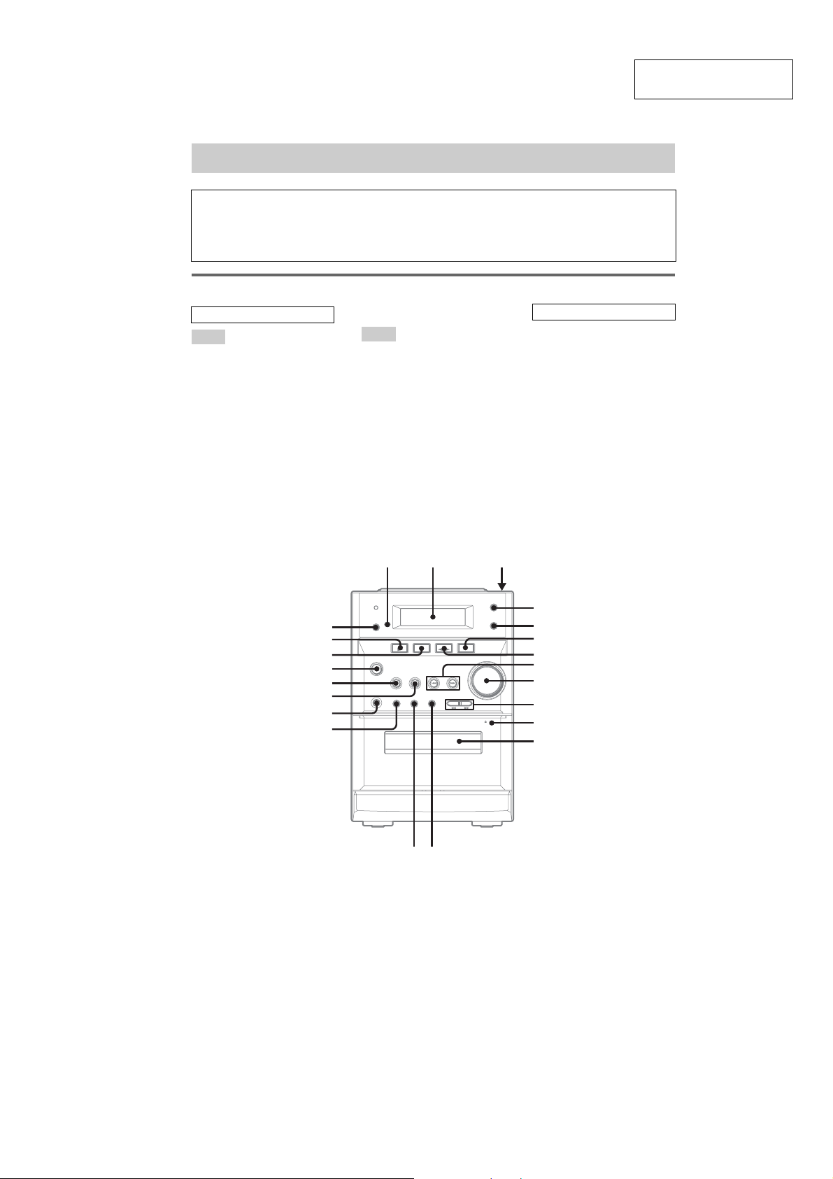
SECTION 2
Illustrati
12 3
GENERAL
List of button locations and reference pages
HCD-EP515
This section is extracted
from instruction manual.
How to use this page
Use this pag e to fin d the lo ca tio n of bu tto n s a n d o th er
parts of the system that are mentioned in the text.
Main unit
ALPHABETICAL ORDER
A – M
BASS/TREBLE 5 (13)
Cassette compartment qs
CD SYNC qd (12)
DIRECTION qg (11, 12, 15)
DISPLAY ws (9, 10, 16)
Display window 2
DSG 4 (13)
MD 6 (17)
P – Z
PHONES jack qh
PLAY MODE qg (6, 7)
PRESET +/– 8 (9)
Remote sensor 1
TUNER BAND w; (8, 9)
TUNING +/– 0 (8 , 9)
VOLUME 9 (14, 15)
on number
r
DISPLAY ws (9, 10, 16)
Name of button/part Reference page
RR
BUTTON DESCRIPTIONS
?/1 (po w e r) ql (5 , 9, 14, 15)
m/M (fast forward/rewin d)
0 (6, 11)
./ > (go back /go fo rw ard)
8 (5, 6, 7, 12, 13, 14, 15)
x (stop) qj (6, 7, 11, 12, 19)
X (pause) qk (6, 11)
zREC PAUSE/START qf (12,
15)
CD N (play) wa (6, 7 )
TAPE nN (play) 7 ( 11, 12,
15)
Z PUSH OPEN/CLOSE (CD
open/close) 3 (6)
Z PUSH OPEN/CLOSE (tape
open/close) qa (11)
ws
wa
w;
ql
qk
qj
qh
qg
4
5
6
7
8
9
q;
qa
qs
qdqf
5
HCD-EP515
./
./
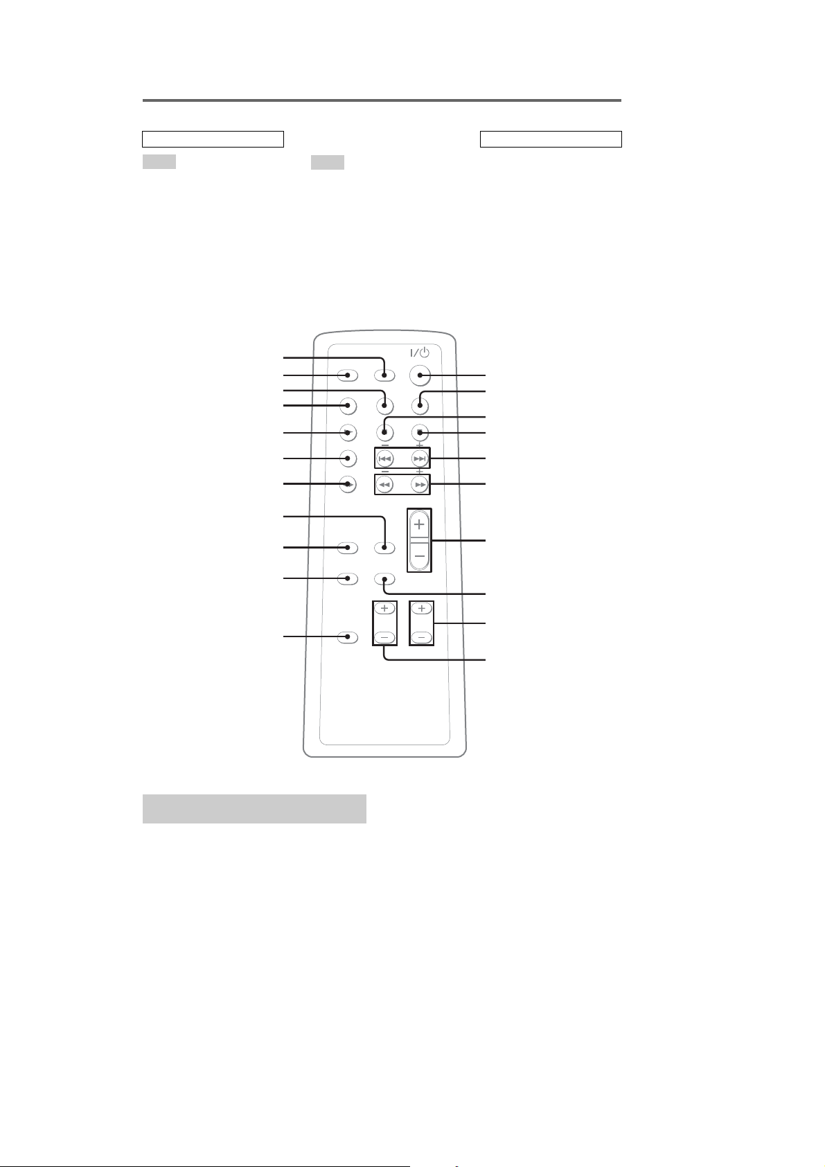
Remote control
ALPHABETICAL ORDER
A – M
BASS +/– 0 (13)
CLEAR 8 (8, 9)
CLOCK/TIMER SELECT w;
(14, 15)
CLOCK/TIMER SET wa (5, 14,
15)
DISPLAY 2 (9, 10, 16)
DSG qa (13)
MD qk (17)
wa
w;
ql
qk
qj
qh
qg
qf
P – Z
PLAY MODE/DIRECTION qd
(6, 7, 11, 12, 15)
PRESET +/– 5 (9)
REPEAT/FM MODE qf (7, 9)
SLEEP ql (13)
TREBLE +/– 9 (13)
TUNER BAND qh (8, 9)
TUNER MEMORY qs (8)
TUNING +/– 6 (8, 9)
VOL +/– 7 (14, 15 )
BUTTON DESCRIPTIONS
?/1 (power) 1 (5, 9, 14, 15)
m/M (fast forward/rewind)
6 (6, 11)
./ > (go back/go forward)
5 (5, 6, 7, 12, 14, 15)
x (stop ) 4 (6, 7, 11, 12, 19)
X (pa us e) 3 (6, 11)
CD N (play) qj (6, 7)
TAPE nN (play) qg (11, 12 ,
15)
1
2
3
4
5
6
qd
qs
qa
Setting the clock
Press ?/1 to turn on the system.
1
Press CLOCK/TIMER SET.
2
Press ./
3
hour.
Press CLOCK/TIMER SET.
4
Press ./
5
minute.
Press CLOCK/TIMER SET.
6
The clock starts working.
To adjust the clock
Press CLOCK/TIMER SET.
1
Press ./> to select “CLOCK”, then
2
press CLOCK/TIMER SET.
Do the same procedures as step 3 to 6
3
above.
> repeatedly to set the
> repeatedly to set the
7
8
9
0
6
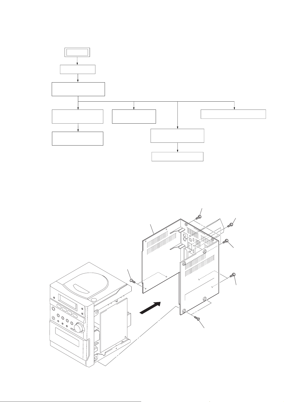
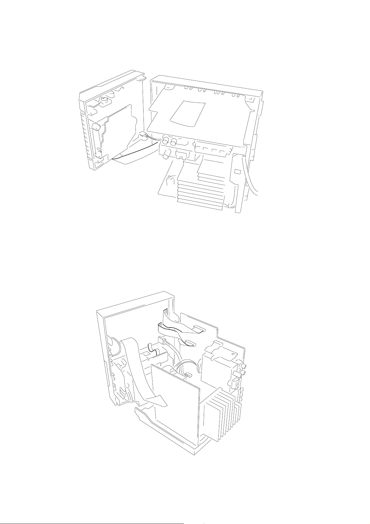
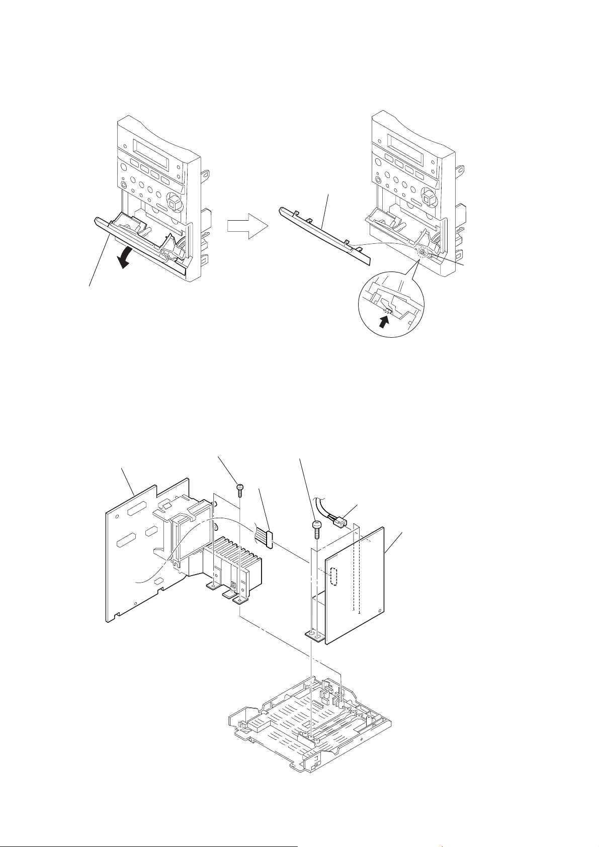
• This set can be disassembled in the order shown below.
)
SET
REAR CABINET
CD CABINET SECTION,
FRONT PANEL SECTION
HCD-EP515
SECTION 3
DISASSEMBLY
CD MECHANISM DECK
(KSM-213EDP)
OPTICAL PICK-UP
(KSS-213E/C2N)
Note: Follow the disassembly procedure in the numerical order given.
CONTROL BOARD,
BACK LIGHT BOARD
3-1. Rear Cabinet
5
two screws
(+K 3
×
5)
7
rear cabinet
TAPE MECHANISM DECK
(CMAL1Z240A)
CASSETTE DOOR ASSY
1
two screws
(+BVTP 3
POWER BOARD , MAIN BOARD
×
10)
2
four screws
(+BVTP 3
3
×
two screws
(+BVTP 3
10)
×
10)
6
two screws
(+K 3
4
×
5)
two screws
(+BVTP 3
×
10
7
HCD-EP515
)
)
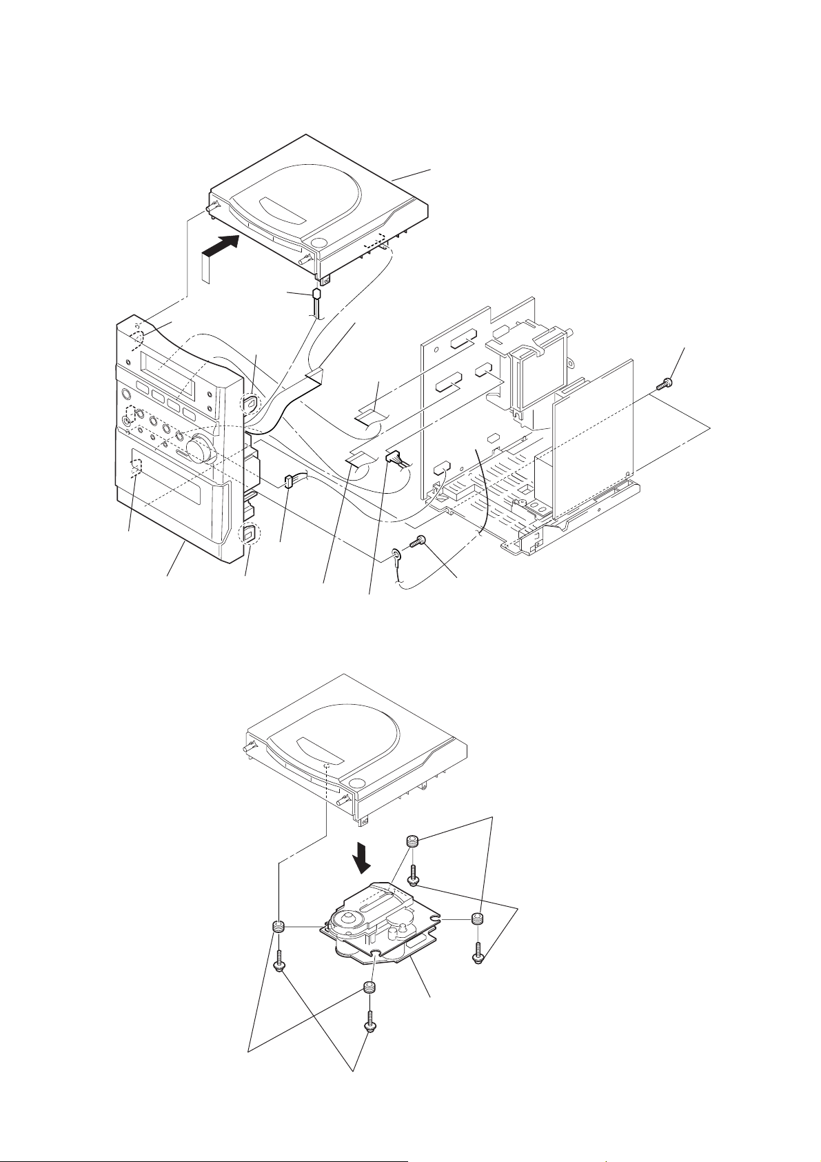
3-2. CD Cabinet Section, Front Panel Section
1
connector
(S800)
4
claw
3
claw
2
w
ire (flat type)
21p (CN101)
6
w
ire (flat type)
20p (CN303)
5
CD cabinet section
qa
two screws
(+BVTP 3
×
10
qd
claw
qf
front panel section
qs
9
connector
(CN307)
claw
7
15p (CN302)
3-3. CD Mechanism Deck (KSM-213EDP)
w
ire (flat type)
8
connector
(CN301)
q;
screw
(+BVTP 3 × 10)
3
two vibration proof rubbers (PNK
1
two screws
(+PWH 2.6
×
10)
5
CD mechanism deck
(KSM-213EDP)
4
two vibration proof rubbers (GRN)
2
two screws
(+PWH 2.6 × 10)
8
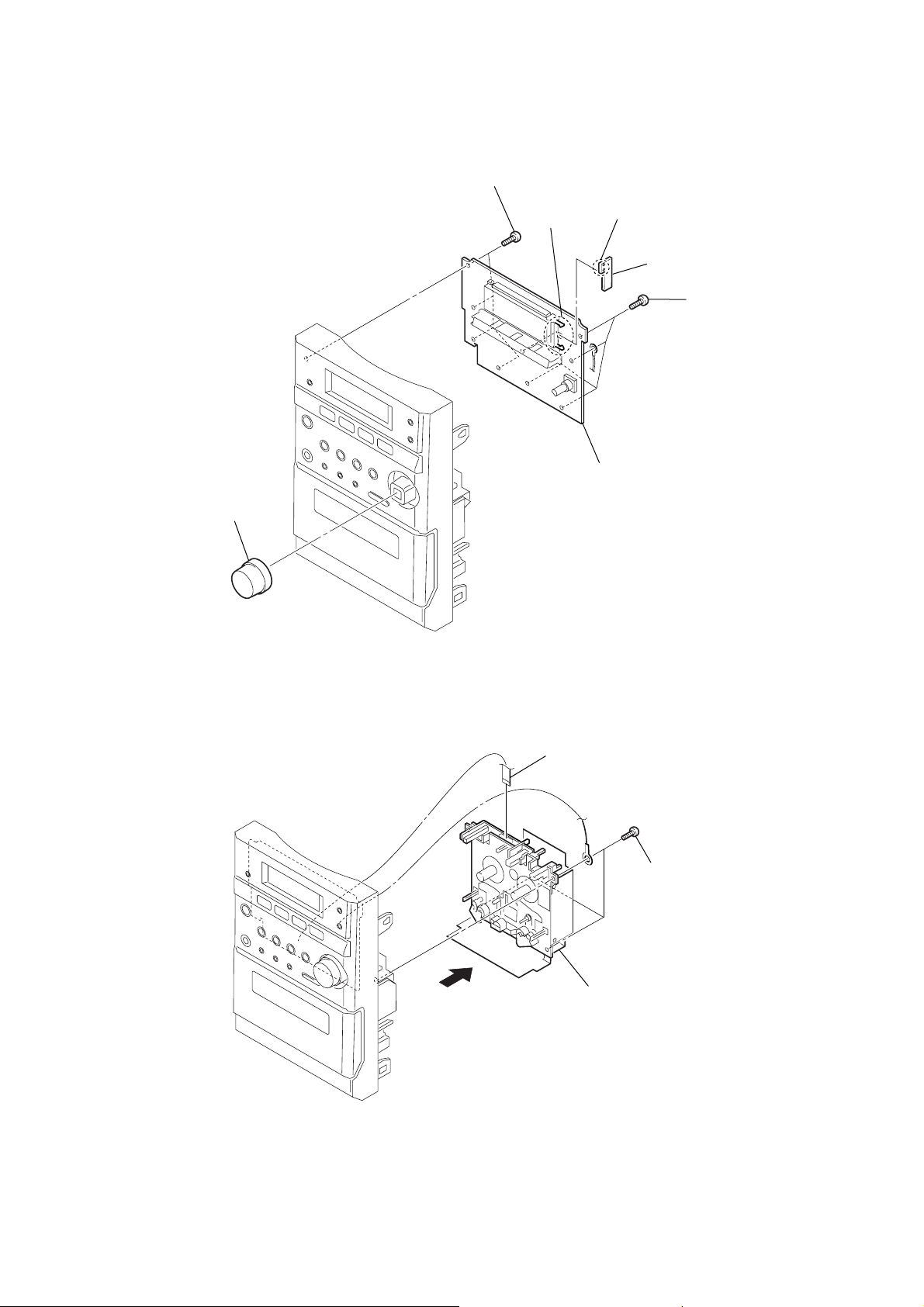
3-4. CONTROL Board, BACK LIGHT Board
)
)
2
four screws
(+BVTP 3
×
10)
6
two
claws
5
Remove the soldering.
7
BACK LIGHT board
4
CONTROL board
3
five screws
(+BVTP 3
HCD-EP515
×
10
1
knob volume
3-5. Tape Mechanism Deck (CMAL1Z240A)
1
w
ire (flat type) 8p
2
three screws
(+BVTP 3
×
10
3
tape mechanism deck
(CMAL1Z240A)
9
HCD-EP515
3-6. Cassette Door Assy
1
Open the cassette door assy.
3
cassette door assy
claw
3-7. POWER Board, MAIN Board
5
6
MAIN board
two screws
(+BVTP 3
×
10)
2
connector
(CN901)
3
four screws
(+BVTP 4
×
12)
1
connector
(AC IN)
2
4
POWER board
10
3-8. Optical Pick-up (KSS-213E/C2N)
6
KSS-213E/C2N
5
sled shaft
1
2
gear (A)
claw
HCD-EP515
4
3
11

HCD-EP515
SECTION 4
MECHANICAL ADJUSTMENTS
Precaution
1. Clean the following parts with a denatured alcohol-moistened
swab:
record/playback heads pinch rollers
erase head rubber belts
capstan idlers
2. Demagnetize the record/playback head with a head demagnetizer.
3. Do not use a magnetized screwdriver for the adjustments.
4. After the adjustments, apply suitable locking compound to the
parts adjusted.
5. The adjustments should be performed with the rated power
supply voltage unless otherwise noted.
Torque Measurement
Mode
FWD
FWD
back tension
REV
REV
back tension
FF/REW
FWD tension
REV tension
Torque meter Meter reading
3.04 – 6.96 mN • m
CQ-102C
CQ-102C
CQ-102RC
CQ-102RC
CQ-201B
CQ-403A
CQ-403R
(31 to 71 g • cm)
(0.43 – 0.98 oz • inch)
0.20 – 0.58 mN • m
(2 to 6 g • cm)
(0.02 – 0.08 oz • inch)
3.04 – 6.96 mN • m
(31 to 71 g • cm)
(0.43 – 0.98 oz • inch)
0.20 – 0.58 mN • m
(2 to 6 g • cm)
(0.02 – 0.08 oz • inch)
6.97 – 14.02 mN • m
(71 to 143 g • cm)
(0.98 – 1.99 oz • inch)
9.8 mN • m or more
(100 g • cm or more)
(1.4 oz • inch or more)
9.8 mN • m or more
(100 g • cm or more)
(1.4 oz • inch or more)
12
+
–
CD board
TP (RFAC)
TP (VC)
oscilloscope
SECTION 5
ELECTRICAL ADJUSTMENTS
HCD-EP515
CD SECTION
Note:
1. CD Block is basically designed to operate without adjustment. Therefore, check each item in order given.
2. Use YEDS-18 disc (3-702-101-01) unless otherwise indicated.
3. Use an oscilloscope with more than 10MΩ impedance.
4. Clean the object lens by an applicator with neutral detergent when the
signal level is low than specified value with the following checks.
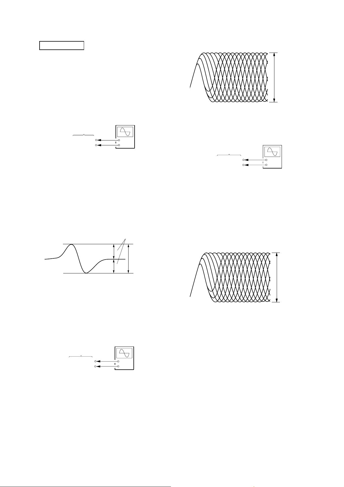
S-curve Check
Connection:
oscilloscope
CD board
TP (FE)
TP (DVC)
Procedure:
1. Connect an oscilloscope to test point TP (FE) and TP (DVC)
on the CD board.
2. Turn the power on.
3. Put the disc (YEDS-18) in and turned power switch on again
and actuate the focus search. (actuate the focus search when
disc table is moving in and out)
4. Check the oscilloscope waveform (S-curve) is symmetrical
between A and B. And confirm peak to peak le vel within 2 ± 1
Vp-p.
S-curve waveform
+
–
symmetry
A
B
within 2
±
1 Vp-p
RFDC signal waveform
VOLT/DIV: 200 mV
TIME/DIV: 500 ns
level: 1.15
±
0.35 Vp-p
Checking Location: CD board (Conductor side)
RFAC Level Check
Connection:
Procedure:
1. Connect an oscilloscope to test point TP (RFA C) and TP (VC)
on the CD board.
2. Turn the power on.
3. Put the disc (YEDS-18) in to playback the number five track.
4. Confirm that oscilloscope waveform is clear and check RF AC
signal level is correct or not.
Note: A clear RFAC signal waveform means that the shape “◊” can be
clearly distinguished at the center of the waveform.
RFAC signal waveform
VOLT/DIV: 200 mV
TIME/DIV: 500 ns
Note: •Try to measure several times to mak e sure than the ratio of A : B
or B : A is more than 10 : 7.
•Take sweep time as long as possible and light up the
brightness to obtain best waveform.
Checking Location: CD board (Conductor side)
RFDC Level Check
Connection:
oscilloscope
CD board
TP (RFDC)
TP (DVC)
+
–
Procedure:
1. Connect an oscilloscope to test point TP (RFDC) and TP (DVC)
on the CD board.
2. Turn the power on.
3. Put the disc (YEDS-18) in to playback the number five track.
4. Confirm that oscilloscope waveform is clear and check RFDC
signal level is correct or not.
Note: A clear RFDC signal waveform means that the shape “◊” can be
clearly distinguished at the center of the waveform.
±
level: 1.35
0.4 Vp-p
Checking Location: CD board (Conductor side) (See page 14)
13
 Loading...