

SONY HC18E Service Manual
DCR-HC17E/HC19E/HC21/HC21E/HC22E/
HC32/HC32E/HC33/HC33E
RMT-830/831
SERVICE MANUAL
Ver 1.1 2005.09
Revision History
Revision History
How to use
How to use
Acrobat Reader
Acrobat Reader
Z MECHANISM (MDX-Z210)
Link
Link
SPECIFICATIONS
SPECIFICATIONS
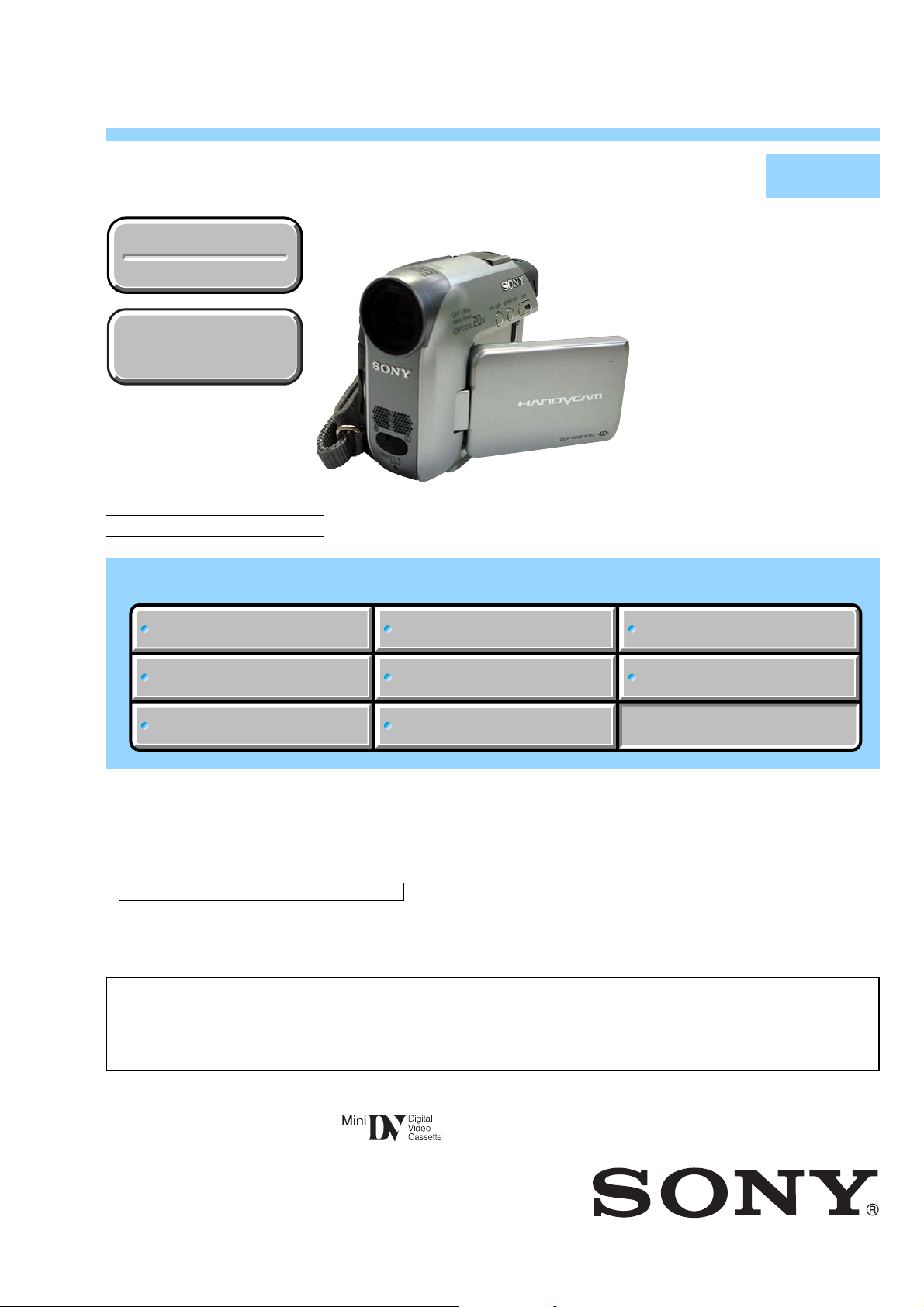
Photo: DCR-HC32
BLOCK DIAGRAMS
BLOCK DIAGRAMS
LEVEL 2
DCR-HC21/HC32
DCR-HC17E/HC19E/HC22E/HC32E
East European Model
North European Model
DCR-HC19E/HC22E/HC32E
DCR-HC21/HC21E/HC32/HC32E
DCR-HC21E/HC32E
DCR-HC21/HC33
DCR-HC21E/HC33E
DCR-HC32/HC32E
PRINTED WIRING BOARDS
PRINTED WIRING BOARDS
US Model
Canadian Model
Korea Model
AEP Model
UK Model
E Model
Australian Model
Hong Kong Model
Brazilian Model
Chinese Model
Tourist Model
SERVICE NOTE
SERVICE NOTE
DISASSEMBLY
DISASSEMBLY
NON MS model: DCR-HC17E/HC19E/HC21/HC21E/HC22E
MS model: DCR-HC32/HC32E/HC33/HC33E
•For ADJUSTMENTS (SECTION 6), refer to SERVICE MANUAL, ADJ (9-876-782-51).
• For INSTRUCTION MANUAL, refer to SERVICE MANUAL, LEVEL 1 (9-876-782-41).
•For MECHANISM ADJUSTMENTS, refer to the “DV MECHANICAL ADJUSTMENT MANUAL VIII
Z (Z200/Z210/Z300/Z310) MECHANISM ” (9-876-724-1[]).
• Reference No. search on printed wiring boards is available.
•Table for differences of function of each model.
•TO TAKE OUT A CASSETTE WHEN NOT EJECT (FORCE EJECT)
• HELP: Sheet attachment positions and procedures of processing the flexible boards/harnesses are shown.
On the VC-376/377 boards
This service manual provides the information that is premised the circuit board replacement service and not intended repair
inside the VC-376/377 boards.
Therefore, schematic diagrams, printed wiring boards, mounted parts location and electrical parts list of the VC-376/377 boards
are not shown.
FRAME SCHEMATIC DIAGRAMS
FRAME SCHEMATIC DIAGRAMS
SCHEMATIC DIAGRAMS
SCHEMATIC DIAGRAMS
REPAIR PARTS LIST
REPAIR PARTS LIST
DCR-HC17E/HC19E/HC21/HC21E/HC22E/HC32/HC32E/HC33/HC33E
9-876-782-31
DIGITAL VIDEO CAMERA RECORDER
2005I0500-1
Sony EMCS Co.
Published by DI Technical Support Department
© 2005.9

System
Video recording
system
DCR-HC32/HC32E/HC33/HC33E:
Still image
recording system
Audio recording
system
Video signal
Usable cassette Mini DV cassette with the
Tape speed SP: Approx. 18.81 mm/s
Recording/
playback time
Fast forward/
rewind time
Viewfinder Electric viewfinder
Image device
Lens Carl Zeiss Vario-Tessar
Focal length
Color temperature
2 rotary heads, Helical
scanning system
Exif V er . 2.2
Rotary heads, PCM system
Quantization: 12 bits (Fs 32 kHz,
stereo 1, stereo 2), 16 bits
(Fs 48 kHz, stereo)
DCR-HC21/HC32/HC33:
NTSC color, EIA standards
DCR-HC17E/HC19E/HC21E/
HC22E/HC32E/HC33E:
PAL color, CCIR standards
LP: Approx. 12.56 mm/s
SP: 60 min
LP: 90 min
(using a DVM60 cassette)
Approx. 2 min 40 s
(using a DVM60 cassette)
(black and white)
3 mm (1/6 type) CCD (Charge
Coupled Device)
DCR-HC32/HC33:
Gross: Approx. 680 000 pixels
Effective (still): Approx.
340 000 pixels
Effective (movie): Approx.
340 000 pixels
DCR-HC21:
Gross: Approx. 680 000 pixels
Effective (movie): Approx.
340 000 pixels
DCR-HC17E/HC19E/HC21E/
HC22E:
Gross: Approx. 800 000 pixels
Effective (movie): Approx.
400 000 pixels
DCR-HC32E/HC33E:
Gross: Approx. 800 000 pixels
Effective (still): Approx.
400 000 pixels
Effective (movie): Approx.
400 000 pixels
Combined power zoom lens
Filter diameter: 25 mm (1 in.)
20 × (Optical), 640 × (Digital,
DCR-HC17E), 800 × (Digital,
DCR-HC19E/HC21/HC21E/
HC22E/HC32/HC32E/HC33/
HC33E)
F=1.8 - 3.1
f=2.3 - 46 mm (3/32 - 1 13/16 in.)
When converted to a 35 mm
still camera
DCR-HC17E/HC19E/HC21/
HC21E/HC22E:
In CAMERA:
44 - 880 mm (1 3/4 - 34 1/32 in.)
DCR-HC32/HC32E/HC33/
HC33E:
In CAMERA-TAPE:
44 ~ 880 mm (1 3/4 - 34 1/32 in.)
In CAMERA-MEMORY:
44 ~ 880 mm (1 3/4 - 34 1/32 in.)
[AUTO], [ONE PUSH],
[INDOOR] (3 200 K),
[OUTDOOR] (5 800 K)
1
*
mark printed
SPECIFICATIONS
Minimum
illumination
*1 “Exif” is a file format for still images, established
by the JEITA (Japan Electronics and Information
Technology Industries Association). Files in this
format can have additional information such as
your camcorder’s setting information at the time of
recording.
*2 Objects unable to be seen due to the dark can be
shot with infrared lighting.
Input/Output connectors
Audio/Video
input/output
(DCR-HC32/
HC32E/HC33/
HC33E)
Audio/Video
output
(DCR-HC17E/
HC19E/HC21/
HC21E/HC22E)
USB jack
(DCR-HC17E/
HC19E/HC21/
HC21E)
LANC jack Stereo mini-minijack (φ 2.5 mm)
DV input/output
(DCR-HC21/
HC21E)
DV output
(DCR-HC17E/
HC19E)
5 lx (lux) (F 1.8)
0 lx (lux) (during NightShot plus
2
function)*
10-pin connector
Input/output auto switch
Video signal: 1 Vp-p, 75 Ω
(ohms), unbalanced
Luminance signal: 1 Vp-p,
75 Ω (ohms), unbalanced
Chrominance signal: 0.286 Vp-p,
75 Ω (ohms, DCR-HC32/HC33),
0.3 Vp-p, 75 Ω (ohms,
DCR-HC32E/HC33E),
unbalanced
Audio signal: 327 mV (at output
impedance more than 47 kΩ
(kilohms)),
Input impedance more than 47 kΩ
(kilohms), Output
impedance with less than 2.2 kΩ
(kilohms)
10-pin connector
Video signal: 1 Vp-p, 75 Ω
(ohms), unbalanced
Luminance signal: 1 Vp-p,
75 Ω (ohms), unbalanced
Chrominance signal: 0.286 Vp-p,
75 Ω (ohms, DCR-HC21),
0.3 Vp-p, 75 Ω (ohms,
DCR-HC17E/HC19E/HC21E/
HC22E), unbalanced
Audio signal: 327 mV (at output
impedance more than 47 kΩ
(kilohms)), Output
impedance with less than 2.2 kΩ
(kilohms)
mini-B
4- pin connector
4- pin connector
LCD screen
Picture
Total dot number
General
Power
requirements
Average power
consumption
Operating
temperature
Storage
temperature
Dimensions
(approx.)
Mass (approx.)
Supplied
accessories
6.2 cm (2.5 type)
123 200 (560 × 220)
DC 7.2 V (battery pack)
DC 8.4 V (AC Adaptor)
DCR-HC32/HC32E/HC33/
HC33E:
During camera recording using
the viewfinder 2.1 W
During camera recording using
the LCD 2.5 W
During camera recording using
the viewfinder and the LCD 2.6 W
DCR-HC17E/HC19E/HC21/
HC21E/HC22E:
During camera recording using
the viewfinder 1.9 W
During camera recording using
the LCD 2.4 W
0 °C to 40 °C (32 °F to 104 °F)
-20 °C to + 60 °C (-4 °F to +
140 °F)
54.7 × 90 × 111.7 mm (2 1/4 ×
3 5/8 × 4 1/2 in.) (w/h/d)
400 g (14 oz) main unit only
460 g (1 lb) including the
NP-FP30 rechargeable battery
pack and DVM60 cassette.
AC Adaptor (1)
Power cord (1)
Handycam Station (1)
(DCR-HC22E/HC32/HC32E/
HC33/HC33E)
Wireless Remote Commander
(1) (DCR-HC19E/HC21/HC21E/
HC22E/HC32/HC32E/HC33/
HC33E)
A/V connecting cable (1)
USB cable (1) (DCR-HC19E/
HC21/HC21E/HC22E/HC32/
HC32E/HC33/HC33E)
Shoulder Strap (1) (DCR-HC19E/
HC21/HC21E/HC22E/HC32/
HC32E/HC33/HC33E)
Rechargeable battery pack
NP-FP30 (1)
CD-ROM “Picture Package
Ver. 1.5” (1)
Shoe cover (1)
Operating Guide (1)
21-pin adaptor (1)
(DCR-HC22E/HC32E)
Conversion 2P adaptor (1)
(DCR-HC21/HC32: E, JE/
HC32E: JE)
“Memory Stick Duo” 16MB (1)
(DCR-HC33/HC33E)
Memory Stick Duo adaptor (1)
(DCR-HC33/HC33E)
See page 5-29
– Continued on next page –
DCR-HC17E/HC19E/HC21/HC21E/HC22E/HC32/HC32E/HC33/HC33E
— 2 —

Handycam Station DCRA-C121
(DCR-HC32/HC32E/HC33/HC33E)
Audio/Video
input/output
USB jack mini-B
DV input/output 4-pin connector
10-pin connector
Input/output auto switch Video
signal: 1 Vp-p, 75 Ω (ohms),
unbalanced
Luminance signal: 1 Vp-p, 75 Ω
(ohms), unbalanced
Chrominance signal: 0.286 Vp-p,
75 Ω (ohms, DCR-HC32/HC33),
0.3 Vp-p, 75 Ω (ohms,
DCR-HC32E/HC33E),
unbalanced
Audio signal: 327 mV (at output
impedance more than 47 kΩ
(kilohms)),
Input impedance more than
47 kΩ (kilohms), Output
impedance with less than 2.2 kΩ
(kilohms)
Handycam Station DCRA-C122
(DCR-HC22E)
Audio/Video
output
USB jack mini-B
DV input/output 4-pin connector
10-pin connector
Video signal: 1 Vp-p, 75 Ω
(ohms), unbalanced
Luminance signal: 1 Vp-p, 75 Ω
(ohms), unbalanced
Chrominance signal: 0.3 Vp-p,
75 Ω (ohms,), unbalanced
Audio signal: 327 mV (at output
impedance more than 47 kΩ
(kilohms)), Otput impedance with
less than 2.2 kΩ (kilohms)
AC Adaptor AC-L25A/L25B
Power
requirements
Current
consumption
Power
consumption
Output voltage DC 8.4 V*
Operating
temperature
Storage
temperature
Dimensions
(approx.)
Mass (approx.) 190 g (6.7 oz) excluding the
* See the label on the AC Adaptor for other
specifications.
AC 100 - 240 V, 50/60 Hz
0.35 - 0.18 A
18 W
0 °C to 40 °C (32 °F to 104 °F)
-20 °C to + 60 °C (-4 °F to +
140 °F)
56 × 31 × 100 mm (2 1/4 × 1 1/4
× 4 in.) (w/h/d) excluding the
projecting parts
power cord
Rechargeable battery pack NP-FP30
Maximum output
voltage
Output voltage DC 7.2 V
Capacity 3.6 wh (500 mAh)
Dimensions
(approx.)
Mass (approx.) 40 g (1.5 oz)
Operating
temperature
Type Lithium ion
Design and specifications are subject to change
without notice.
DC 8.4 V
31.8 × 18.5 × 40.5 mm (1 5/16
× 3/4 × 1 13/16 in.) (w/h/d)
0 °C to 40 °C (32 °F to 104 °F)
DCR-HC17E/HC19E/HC21/HC21E/HC22E/HC32/HC32E/HC33/HC33E
— 3 —

Table for differences of function
NON MS model
Model DCR-HC17E DCR-HC19E DCR-HC21 DCR-HC21E DCR-HC22E
Destination AEP, NE, EE AEP, UK, NE, EE
Color system PAL PAL NTSC PAL PAL
Memory Stick Duo ××× ××
A/V jack OUT OUT OUT OUT OUT
DV Interface OUT OUT IN/OUT IN/OUT IN/OUT (Note)
Remote commander × a (RMT-830) a (RMT-830) a (RMT-830) a (RMT-830)
Cradle (Handycam Station) ××× ×a
CR board ××× ×CR-050
VC board VC-376 VC-376 VC-376 VC-376 VC-376
MS model
Model DCR-HC32 DCR-HC32E DCR-HC33 DCR-HC33E
Destination
US, CND, E, KR, AEP, UK, NE, EE,
JE E, HK, AUS, JE
Color system NTSC PAL NTSC PAL
Memory Stick Duo aaa a
A/V jack IN/OUT IN/OUT IN/OUT IN/OUT
DV Interface IN/OUT (Note) IN/OUT (Note) IN/OUT (Note) IN/OUT (Note)
Remote commander a (RMT-831) a (RMT-831) a (RMT-831) a (RMT-831)
Cradle (Handycam Station) aaa a
CR board CR-050 CR-050 CR-050 CR-050
VC board VC-377 VC-377 VC-377 VC-377
US, CND, E, KR,
BR
BR CH
E, HK, AUS, CH AEP, UK, NE, EE
Note: DV Interface on the Cradle (Handycam Station)
•Abbreviation
AUS: Australian model
BR : Brazilian model
CH : Chinese model
CND: Canadian model
EE : East European model
HK : Hong Kong model
JE : Tourist model
KR : Korean model
NE : North European model
DCR-HC17E/HC19E/HC21/HC21E/HC22E/HC32/HC32E/HC33/HC33E
— 4 —

Danger of explosion if battery is incorrectly replaced.
Replace only with the same or equivalent type.
CAUTION
SAFETY-RELATED COMPONENT WARNING!!
COMPONENTS IDENTIFIED BY MARK 0 OR DOTTED LINE WITH
MARK 0 ON THE SCHEMATIC DIAGRAMS AND IN THE PARTS
LIST ARE CRITICAL TO SAFE OPERATION. REPLACE THESE
COMPONENTS WITH SONY PARTS WHOSE PART NUMBERS
APPEAR AS SHOWN IN THIS MANUAL OR IN SUPPLEMENTS
PUBLISHED BY SONY .
After correcting the original service problem, perform the following
safety checks before releasing the set to the customer.
1. Check the area of your repair for unsoldered or poorly-soldered
connections. Check the entire board surface for solder splashes
and bridges.
2. Check the interboard wiring to ensure that no wires are
"pinched" or contact high-wattage resistors.
3. Look for unauthorized replacement parts, particularly
transistors, that were installed during a previous repair. Point
them out to the customer and recommend their replacement.
4. Look for parts which, through functioning, show obvious signs
of deterioration. Point them out to the customer and
recommend their replacement.
5. Check the B+ voltage to see it is at the values specified.
6. FLEXIBLE Circuit Board Repairing
•Keep the temperature of the soldering iron around 270°C
during repairing.
• Do not touch the soldering iron on the same conductor of the
circuit board (within 3 times).
• Be careful not to apply force on the conductor when soldering
or unsoldering.
DCR-HC17E/HC19E/HC21/HC21E/HC22E/HC32/HC32E/HC33/HC33E
ATTENTION AU COMPOSANT AYANT RAPPORT
À LA SÉCURITÉ!
LES COMPOSANTS IDENTIFÉS P AR UNE MARQUE 0 SUR LES
DIAGRAMMES SCHÉMA TIQUES ET LA LISTE DES PIÈCES SONT
CRITIQUES POUR LA SÉCURITÉ DE FONCTIONNEMENT. NE
REMPLACER CES COMPOSANTS QUE PAR DES PIÈSES SONY
DONT LES NUMÉROS SONT DONNÉS DANS CE MANUEL OU
DANS LES SUPPÉMENTS PUBLIÉS PAR SONY.
SAFETY CHECK-OUT
Unleaded solder
Boards requiring use of unleaded solder are printed with the leadfree mark (LF) indicating the solder contains no lead.
(Caution: Some printed circuit boards may not come printed with
the lead free mark due to their particular size.)
: LEAD FREE MARK
Unleaded solder has the following characteristics.
• Unleaded solder melts at a temperature about 40°C higher than
ordinary solder.
Ordinary soldering irons can be used but the iron tip has to be
applied to the solder joint for a slightly longer time.
Soldering irons using a temperature regulator should be set to
about 350°C.
Caution: The printed pattern (copper foil) may peel away if the
heated tip is applied for too long, so be careful!
• Strong viscosity
Unleaded solder is more viscous (sticky, less prone to flow) than
ordinary solder so use caution not to let solder bridges occur such
as on IC pins, etc.
• Usable with ordinary solder
It is best to use only unleaded solder but unleaded solder may
also be added to ordinary solder.
— 5 —

TABLE OF CONTENTS
Section Title Page Section Title Page
1. SERVICE NOTE
1-1. Note for Repair ································································ 1-1
1-2. Power Supply During Repairs········································· 1-1
1-3. To Take Out a Cassette when not Eject (Force Eject) ·····1-2
1-4. Self-diagnosis Function··················································· 1-2
1-4-1.Self-diagnosis Function···················································1-2
1-4-2.Self-diagnosis Display·····················································1-2
1-4-3.Self-diagnosis Code Table···············································1-3
2. DISASSEMBLY
2-1. Disassembly·····································································2-1
2-2. Mechanism Deck Service Position··································2-5
2-3. LCD Service Position······················································ 2-7
2-4. The Method of Attachment of FP-185 Flexible Board····2-8
2-5. Circuit Boards Location ··················································2-9
2-6. Flexible Boards Location ··············································2-10
3. BLOCK DIAGRAMS
3-1. Block Diagrams (Non MS model)···································3-1
3-1-1.Overall Block Diagram (1/5) (Non MS model) ··············3-1
3-1-2.Overall Block Diagram (2/5) (Non MS model) ··············3-3
3-1-3.Overall Block Diagram (3/5) (Non MS model) ··············3-5
3-1-4.Overall Block Diagram (4/5) (Non MS model) ··············3-7
3-1-5.Overall Block Diagram (5/5) (Non MS model) ··············3-9
3-1-6.Power Block Diagram (1/3) (Non MS model) ··············3-11
3-1-7.Power Block Diagram (2/3) (Non MS model) ··············3-13
3-1-8.Power Block Diagram (3/3) (Non MS model) ··············3-15
3-2. Block Diagrams (MS model) ········································3-17
3-2-1.Overall Block Diagram (1/6) (MS model) ····················3-17
3-2-2.Overall Block Diagram (2/6) (MS model) ····················3-19
3-2-3.Overall Block Diagram (3/6) (MS model) ····················3-21
3-2-4.Overall Block Diagram (4/6) (MS model) ····················3-23
3-2-5.Overall Block Diagram (5/6) (MS model) ····················3-25
3-2-6.Overall Block Diagram (6/6) (MS model) ····················3-27
3-2-7.Power Block Diagram (1/3) (MS model) ······················3-29
3-2-8.Power Block Diagram (2/3) (MS model) ······················3-31
3-2-9.Power Block Diagram (3/3) (MS model) ······················3-33
4-3. Printed Wiring Boards ···················································4-79
CD-533 ··········································································4-81
PD-237···········································································4-91
CR-050 ··········································································4-93
SI-042 ············································································4-94
LB-109···········································································4-94
JK-278 ···········································································4-95
MS-249 ··········································································4-96
FP-180, FP-186, FP-187 FLEXIBLE····························4-97
FP-826, FP-467, FP-228 FLEXIBLE····························4-99
4-4. Waveforms ···································································4-101
4-5. Mounted Parts Location ··············································4-117
5. REPAIR PARTS LIST
5-1. Exploded V iews ····························································5-2
5-1-1. Overall Assembly··························································5-2
5-1-2. F Panel Block································································5-3
5-1-3. Lens Block ····································································5-4
5-1-4. Cabinet (R) Block ·························································5-5
5-1-5. CS Block ·······································································5-6
5-1-6. Bat EVF Block······························································5-7
5-1-7. Mechanism Deck ··························································5-8
5-1-8. LS Chassis Block Assembly ·········································5-9
5-1-9. Mechanism Chassis Block Assembly ·························5-10
5-2. Electrical Parts List ·····················································5-11
4. PRINTED WIRING BOARDS AND
SCHEMATIC DIAGRAMS
4-1. Frame Schematic Diagrams·············································4-1
4-2. Schematic Diagrams························································4-5
CD-533 (CCD IMAGER)················································4-7
PD-237 (LCD DRIVE, BACKLIGHT DRIVE)············4-65
CR-050 (CRADLE TERMINAL) ·································4-67
SI-042 (REMOTE COMMANDER RECEIVER,
PITCH/YAW SENSOR) ················································4-69
FP-182 FLEXIBLE ·······················································4-71
JK-278 (JACK) ······························································4-71
MS-249 (MS CONNECTOR) ·······································4-71
LB-109 (EVF, EVF BACKLIGHT) ······························ 4-73
FP-186 FLEXIBLE (PANEL REVERSE DETECT) ···· 4-73
FP-180 FLEXIBLE (DC IN) ········································· 4-74
FP-187 FLEXIBLE (CONTROL SWITCH)·················4-74
FP-826, FP-467, FP-228 FLEXIBLE····························4-75
CONTROL KEY BLOCK (SS10300) ··························4-77
CONTROL KEY BLOCK (SB9000)····························4-78
DCR-HC17E/HC19E/HC21/HC21E/HC22E/HC32/HC32E/HC33/HC33E
— 6 —
1-1. NOTE FOR REPAIR
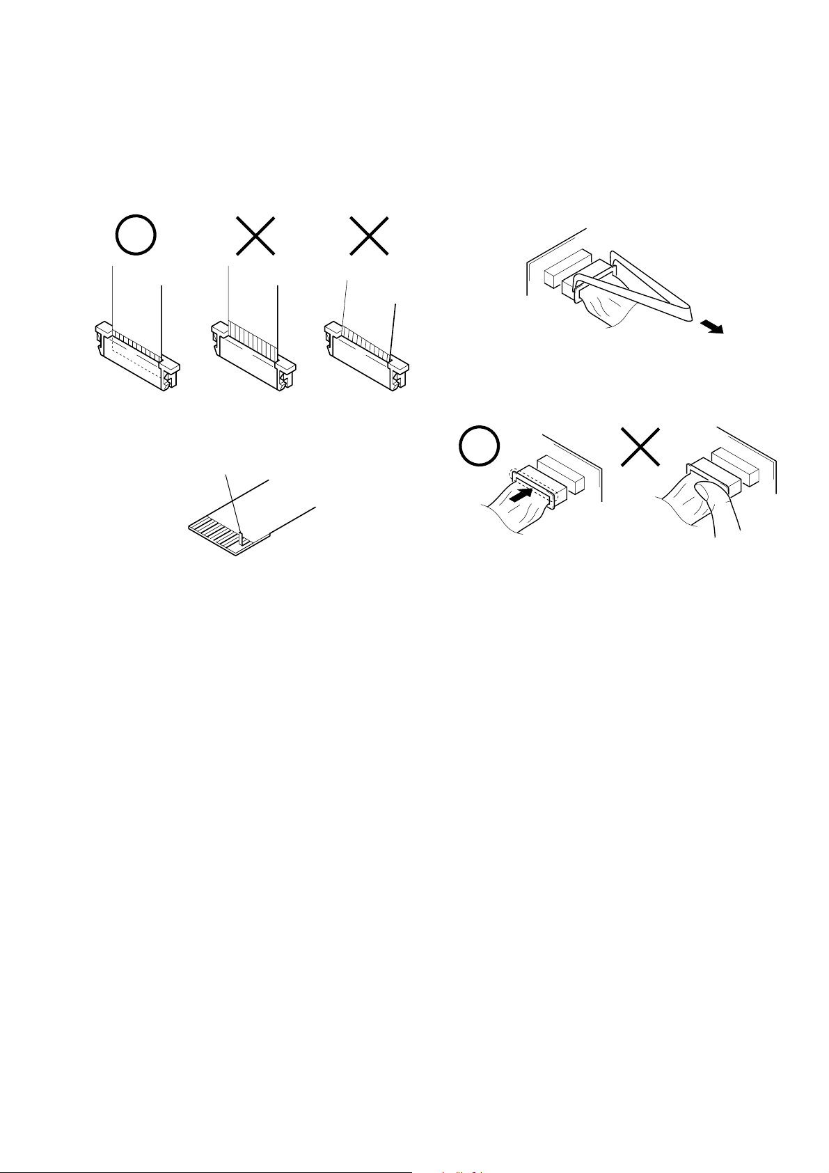
When installing a connector, don’t press down at wire of connector.
It is possible that a wire is snapped.
1. SERVICE NOTE
Make sure that the flat cable and flexible board are not cracked of
bent at the terminal.
Do not insert the cable insufficiently nor crookedly.
Cut and remove the part of gilt
which comes off at the point.
(Be careful or some
pieces of gilt may be left inside)
When remove a connector, don’t pull at wire of connector.
It is possible that a wire is snapped.
1-2. POWER SUPPLY DURING REPAIRS
In this unit, about 10 seconds after power is supplied to the battery terminal using the regulated power supply (8.4V), the po wer is shut of f so
that the unit cannot operate.
These following method is available to prevent this.
Method:
Use the AC power adaptor (AC-L25A/L25B).
DCR-HC17E/HC19E/HC21/HC21E/HC22E/HC32/HC32E/HC33/HC33E
1-1

1-3. TO TAKE OUT A CASSETTE WHEN NOT EJECT (FORCE EJECT)
1 Refer to “2. DISASSEMBLY” to remove the mechanism deck block.
2 Disconnect the CN9002 of VC-376 board (NON MS model) or CN6002 of VC-377 board (MS model).
3 Supply +4.5V from the DC power supply to the loading motor and unload with a pressing the cassette compartment.
NON MS model: DCR-HC17E/HC19E/HC21/HC21E/HC22E
MS model: DCR-HC32/HC32E/HC33/HC33E
Disconnect the CN9002 of VC-376 board (NON MS model)
or CN6002 of VC-377 board (MS model).
Loading motor
DC power supply (+4.5Vdc)
CN9002 (NON MS model)/
CN6002 (MS model)
1-4. SELF-DIAGNOSIS FUNCTION
1-4-1. Self-diagnosis Function
When problems occur while the unit is operating, the self-diagnosis
function starts working, and displays on the viewfinder or LCD
screen what to do. This function consists of two display; selfdiagnosis display and service mode display.
Details of the self-diagnosis functions are provided in the Instruction
manual.
Viewfinder or LCD screen
C : 3 1 : 1 1
Blinks at 3.2Hz
VC-376/VC-377 board
1-4-2. Self-diagnosis Display
When problems occur while the unit is operating, the counter of the
viewfinder or LCD screen shows a 4-digit display consisting of an
alphabet and numbers, which blinks at 3.2 Hz. This 5-character
display indicates the “repaired by:”, “block” in which the problem
occurred, and “detailed code” of the problem.
3 1C
Repaired by:
C : Corrected by customer
H : Corrected by dealer
E : Corrected by service
engineer
DCR-HC17E/HC19E/HC21/HC21E/HC22E/HC32/HC32E/HC33/HC33E
Indicates the appropriate
step to be taken.
E.g.
31 ....Reload the tape.
32 ....Turn on power again.
Block
1 1
Detailed Code
Refer to “1-4-3. Self-diagnosis Code Table”.
1-2

1-4-3. Self-diagnosis Code Table
Self-diagnosis Code
Repaired by:
C
C
C
C
C
C
C
C
C
C
C
C
C
C
C
C
C
C
C
C
C
C
C
C
C
C
C
C
C
Block
Function
04
21
22
31
31
31
31
31
31
31
31
31
31
31
31
31
32
32
32
32
32
32
32
32
32
32
32
32
32
Detailed
Code
00
00
00
10
11
20
21
22
23
30
31
40
41
42
43
44
10
11
20
21
22
23
30
31
40
41
42
43
44
Symptom/State
Non-standard battery is used.
Condensation.
Video head is dirty.
LOAD direction. Loading does not
complete within specified time
UNLOAD direction. Loading does not
complete within specified time
T reel side tape slacking when unloading
S reel
side tape slacking when unloading
T reel fault.
S reel fault.
FG fault when starting capstan.
FG fault during normal capstan operations.
FG fault when starting drum.
PG fault when starting drum.
FG fault during normal drum operations.
PG fault during normal drum operations.
Phase fault during normal drum operations.
LOAD direction loading motor time-
out.
UNLOAD direction loading motor
time-out.
T reel side tape slacking when
unloading.
S reel side tape slacking when
unloading.
T reel fault.
S reel fault.
FG fault when starting capstan.
FG fault during normal capstan
operations.
FG fault when starting drum.
PG fault when starting drum.
FG fault during normal drum
operations.
PG fault during normal drum
operations.
Phase fault during normal drum
operations.
Correction
Use the InfoLITHIUM battery.
Remove the cassette, and insert it again after one hour.
Clean with the optional cleaning cassette.
Load the tape again, and perform operations from the beginning.
Load the tape again, and perform operations from the beginning.
.
Load the tape again, and perform operations from the beginning.
.
Load the tape again, and perform operations from the beginning.
Load the tape again, and perform operations from the beginning.
Load the tape again, and perform operations from the beginning.
Load the tape again, and perform operations from the beginning.
Load the tape again, and perform operations from the beginning.
Load the tape again, and perform operations from the beginning.
Load the tape again, and perform operations from the beginning.
Load the tape again, and perform operations from the beginning.
Load the tape again, and perform operations from the beginning.
Load the tape again, and perform operations from the beginning.
Remove the battery or power cable, connect, and perform
operations from the beginning.
Remove the battery or power cable, connect, and perform
operations from the beginning.
Remove the battery or power cable, connect, and perform
operations from the beginning.
Remove the battery or power cable, connect, and perform
operations from the beginning.
Remove the battery or power cable, connect, and perform
operations from the beginning.
Remove the battery or power cable, connect, and perform
operations from the beginning.
Remove the battery or power cable, connect, and perform
operations from the beginning.
Remove the battery or power cable, connect, and perform
operations from the beginning.
Remove the battery or power cable, connect, and perform
operations from the beginning.
Remove the battery or power cable, connect, and perform
operations from the beginning.
Remove the battery or power cable, connect, and perform
operations from the beginning.
Remove the battery or power cable, connect, and perform
operations from the beginning.
Remove the battery or power cable, connect, and perform
operations from the beginning.
DCR-HC17E/HC19E/HC21/HC21E/HC22E/HC32/HC32E/HC33/HC33E
1-3
Self-diagnosis Code
Repaired by:
E
E
Block
Function
61
61
Detailed
Code
00
10
Symptom/State
Difficult to adjust focus
(Cannot initialize focus.)
Zoom operations fault
(Cannot initialize zoom lens.)
Focus lens intializing failure and zoom
E
61
11
lens initializing failure occur
simultaneously.
Steadyshot function does not work well.
E
62
00
(With pitch angular velocity sensor output
stopped.)
Steadyshot function does not work well.
E
62
01
(With yaw angular v elocity sensor output
stopped.)
Note:
Focus reset sensor
Focus motor drive circuit
Zoom reset sensor
Zoom motor drive circuit
Pin wa of CN3101 on VC-376 board (NON MS model)
Pin wa of CN3701 on VC-377 board (MS model)
IC3101 of VC-376 board (NON MS model)
IC3707 of VC-377 board (MS model)
Pin qh of CN3101 on VC-376 board (NON MS model)
Pin qh of CN3701 on VC-377 board (MS model)
IC3101 of VC-376 board (NON MS model)
IC3707 of VC-377 board (MS model)
NON MS model: DCR-HC17E/HC19E/HC21/HC21E/HC22E
MS model: DCR-HC32/HC32E/HC33/HC33E
Correction
Inspect the lens block focus reset sensor (Note) when focusing is
performed when the touch panel is operated in the focus manual
mode and the focus motor drive circuit (Note) when the focusing
is not performed.
Inspect the lens block zoom reset sensor (Note) when zooming is
performed when the zoom switch is operated and the zoom motor
drive circuit (Note) when zooming is not performed.
Inspect the flexible board for breakage or loose connection.
If not faulty, inspect the focus and zoom motor drive circuit (Note).
Inspect pitch angular velocity sensor (SE601 of SI-042 board)
peripheral circuits.
Inspect yaw angular velocity sensor (SE602 of SI-042 board)
peripheral circuits.
DCR-HC17E/HC19E/HC21/HC21E/HC22E/HC32/HC32E/HC33/HC33E
1-4E
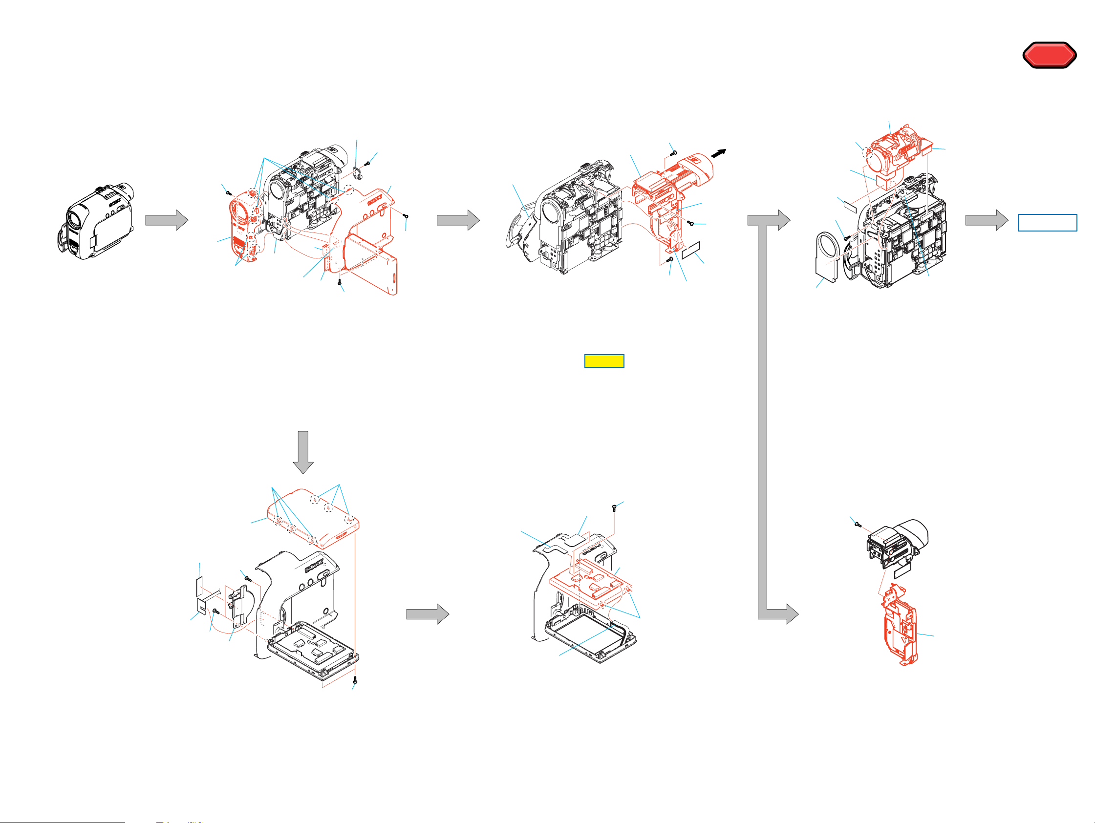
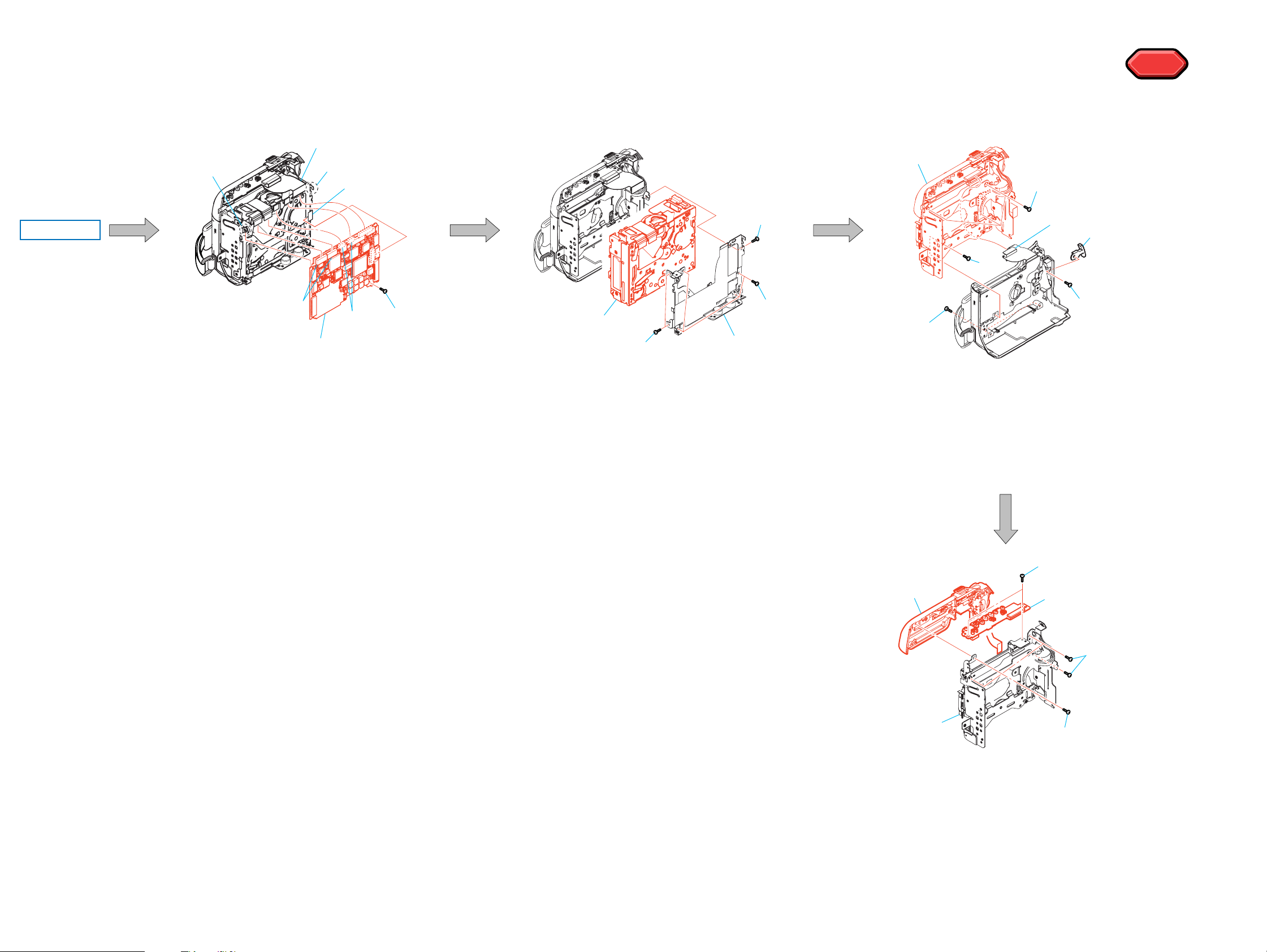
2. DISASSEMBLY
The following flow chart shows the disassembly procedure.
2-1. DISASSEMBLY
Non Cradle model: DCR-HC17E/HC19E/HC21/HC21E
Cradle model: DCR-HC22E/HC32E/HC33/HC33E
4
3
6
5
4
1 P2 lock ace screw (M1.7)
2 Cpc lid
3 Screw (M1.7)
4 Claw
5 Flexible flat cable (FFC-038): CN603
6 F panel block
7 FP-190 flexible board: CN1003 (cradle model)
8 FP-185 flexible board: CN1006
9 FP-187 flexible board: CN1002
0 Cabinet (R) block
x8
x7
9
8
7
3
x1
Non MS model: DCR-HC17E/HC19E/HC21/HC21E/HC22E
MS model: DCR-HC32/HC32E/HC33/HC33E
2
1
0
3
6
1 P2 lock ace screw (M1.7)
2 P2 lock ace screw (M1.7)
3 Slide the EVF block.
4 P2 tappping screw
5 Tape (A)
6 Open the cabinet (G) block.
7 FP-180 flexible board: CN2001
8 FP-181 flexible board: CN7001 (MS model)/
CN9301 (non MS model)
9 BAT EVF block
x2
HELP
x1
9
x1
x1
1
2
7
8
5
3
4
7
6
4
3
2
5
6
1
1 Cushion (F2)
2 Tape (W)
3 Flexible board: CN 3101 (VC-376 board)/
CN3701 (VC-377 board)
4 FP-178 flexible board: CN3002 (VC-376 board)/
CN3101 (VC-377 board)
5 P2 lock ace screw (M1.7)
6 Boss
7 Lens block
x1
x1
x2
HELP
HELP
to Page 2-3
1
5
4
2
3
1 Tape (A)
2 P2 tapping screw
3 Hinge blind
4 FP-187 flexible board
5 Tapping screw
6 P2 tapping screw
7 Claw
8 P cabinet (C) 103
DCR-HC17E/HC19E/HC21/HC21E/HC22E/HC32/HC32E/HC33/HC33E
8
x6
7
x1
7
4
1
2
6
5
3
6
x2
x1
x2
2-1 2-2
1 FP-185 flexible board: CN601
2 FP-186 flexible board: CN609
3 Control key block (SB9000): CN602
4 P2 tapping screw
5 Claw
6 PD-237 board, D901, LCD901
x2
x1
1
1 Ccrew (M1.7)
2 BT panel block
2
x1
6
5
6
1
7
5
HELP
HELP
from Page 2-2
2
7
1 Flexible board: CN1001
2 Connector
CN6002, 6003 (VC-377 board)
3 P2 lock ace screw (M1.7)
4 Connector x2: CN6501, 9001 (VC-376 board)/
CN4301, 6001 (VC-377 board)
5 FP-182 flexible board: CN1008
6 Hook
7 VC-376 board/VC-377 board
x2
x2
: CN9002, 9003 (VC-376 board)/
4
x1
3
4
1
1 P2 lock ace screw (M1.7)
2 Screw (M1.4x1.5)
3 MD frame block
4 Mechanism deck
x4
x3
3
1
2
1
4
6
1 Flexible board: CN704
2 P2 lock ace screw (M1.7)
3 Eject knob
4 P2 lock ace screw (M1.7)
5 Tapping screw
6 P2 lock ace screw (M1.7)
7 CS block
x3
3
2
x1
x1
x2
4
3
5
1 P2 tapping screw (M1.7)
2 P2 lock ace screw (M1.7)
3 Control key block (SS10300)
4 P2 lock ace screw (M1.7)
5 CS frame block
6 JK-278 board
6
1
2
x3
x1
x2
DCR-HC17E/HC19E/HC21/HC21E/HC22E/HC32/HC32E/HC33/HC33E
2-3 2-4
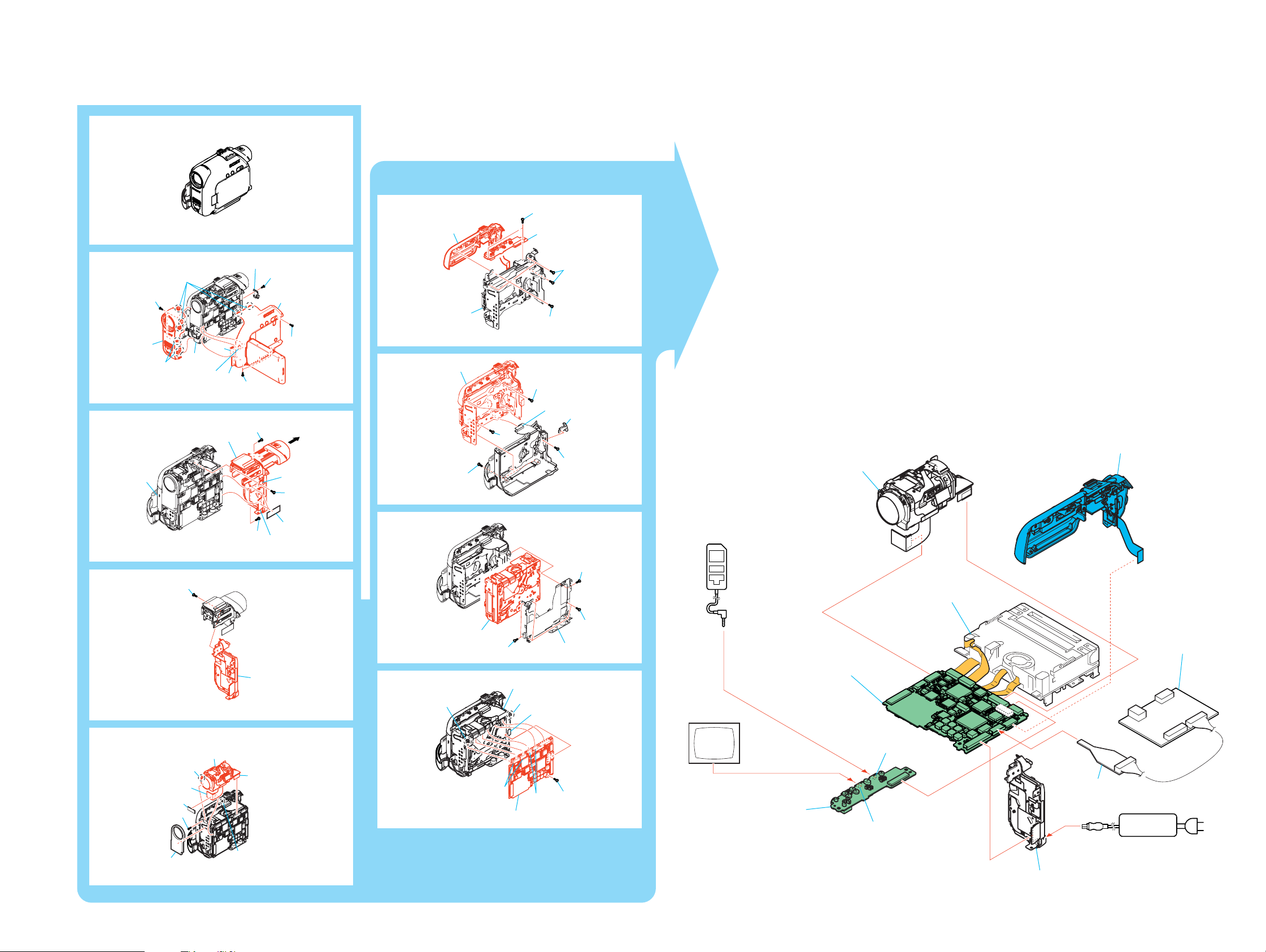
2-2. MECHANISM DECK SERVICE POSITION
2
4
3
6
4
6
8
5
9
7
9
1
0
3
3
1
2
3
8
4
5
7
Connection to Check the Mechanism deck
To check the mechanism deck, set the Camera or VTR to the "Forced power ON" mode.
(Or, connect the control key block (SS10300) to the CN1001 of VC-376/VC-377 board and set the power switch
to the "CAMERA" or "PLAY/EDIT" position.)
Operate the VTR function using the adjustment remote commander
4
3
5
7
4
6
6
1
2
5
1
3
2
Adjustment
remote commander
(RM95)
(with the HOLD switch set in the OFF position).
Setting the "Forced Camera Power ON" mode
1) Select page: 0, address: 01, and set data: 01.
2) Select page: A (MS model)/ D (Non MS model),
address: 10, set data: 01 and press
the PAUSE button of the adjustment remote
commander.
Setting the "Forced VTR Power ON" mode
1) Select page: 0, address: 01, and set data: 01.
2) Select page: A (MS model)/ D (Non MS model),
address: 10, set data: 02 and
press the PAUSE button of the adjustment remote
commander.
Non MS model: DCR-HC17E/HC19E/HC21/HC21E/HC22E
MS model: DCR-HC32/HC32E/HC33/HC33E
*: To eject a cassette, connect the cabinet (L) block assembly.
Lens block
Exiting the "Forced Power ON" mode
1) Select page: 0, address: 01, and set data: 01.
2) Select page: A (MS model)/ D (Non MS model),
address: 10, data: 00, and press the PAUSE
button of the adjustment remote commander.
3) Select page: 0, address: 01, and set data: 00.
Control key block
(SS10300)
1
1
4
1
2
3
Mechanism deck
*
I/F unit for LANC control
(J-6082-521-A)
VC-376 board (Non MS model)
2
6
5
6
1
Color monitor
VC-377 board (MS model)
8
7
6
3
2
5
4
2
7
3
4
JK-278 board
LANC jack
A/V jack (MS model)
1
CPC-15
(J-6082-564-A)
AC adaptor
AC IN
A/V OUT jack (Non MS model)
1
6
BT panel block
DCR-HC17E/HC19E/HC21/HC21E/HC22E/HC32/HC32E/HC33/HC33E
2-5 2-6
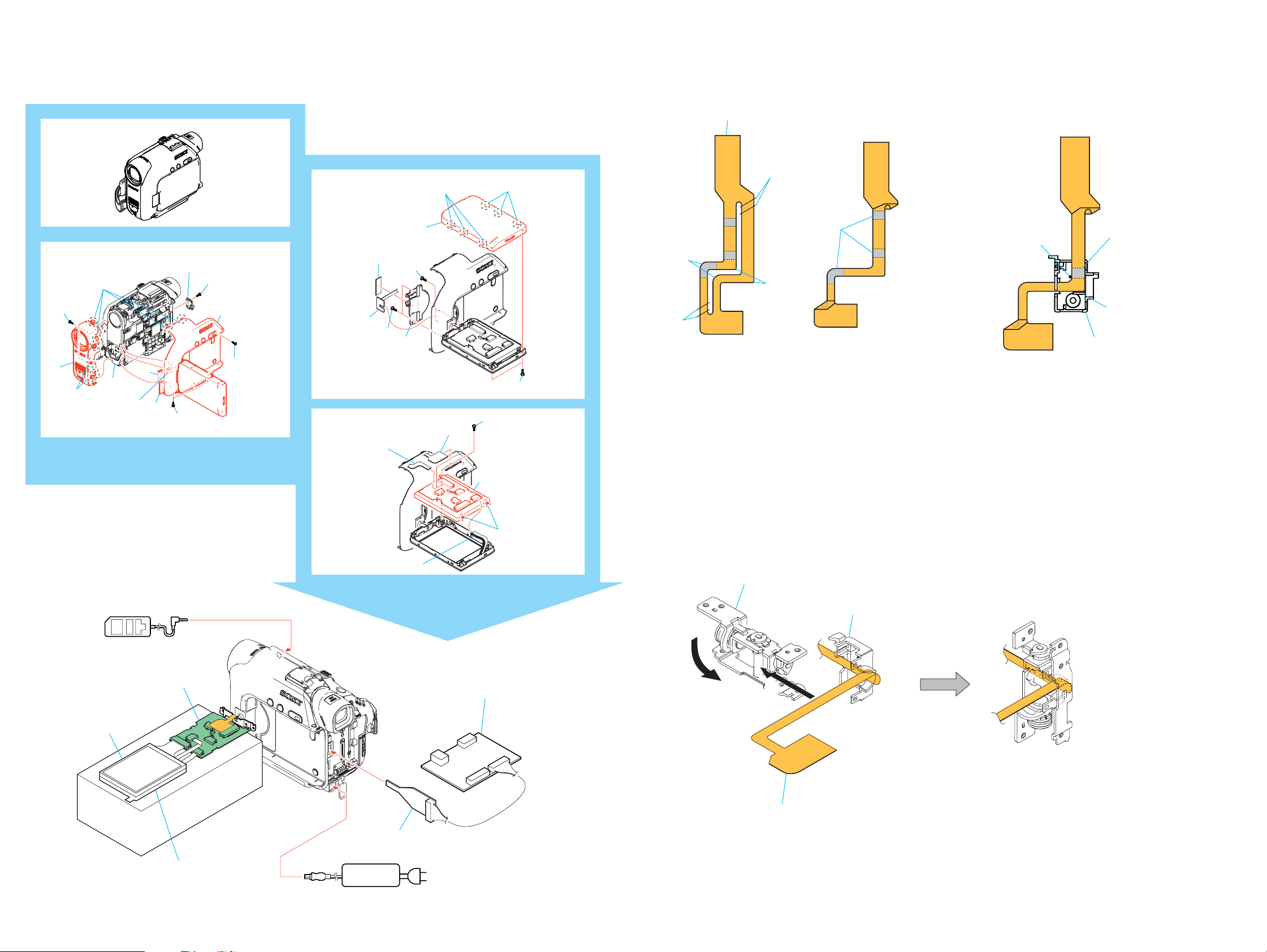
2-3. LCD SERVICE POSITION
2-4. THE METHOD OF ATTACHMENT OF FP-185 FLEXIBLE BOARD
6
3
4
4
5
9
8
7
3
2
1
0
3
4
1
2
2
3
5
8
7
1
4
7
6
FP-185 flexible board
Fold
Adhesive tape
A
B
Fold
1The A and A, B and B section are united
and an angle is folded.
2Set the hinge cover (M) inthe shown below.
Adhesive tape
Boss
Rib
Hinge cover (M)
Adjustment
remote commander
(RM95)
Lcd panel
PD-237 board
6
3Set the FP-185 flexible board in the direction of arrow A,
5
3
I/F unit for LANC control
(J-6082-521-A)
8
1
and then turn the hinge (103) assembly in the direction of arrow
Hinge (103) assembly
Hinge cover (M)
B
A
FP-185 flexible board
B.
Lighit guide plate block
DCR-HC17E/HC19E/HC21/HC21E/HC22E/HC32/HC32E/HC33/HC33E
CPC-15
(J-6082-564-A)
AC adaptor
AC IN
2-7 2-8
FP-181 flexible
FP-185 flexible
FP-178 flexible
FP-182 flexible
FP-187 flexible
Control key block
(SS10300)
Control key block
(SB9000)
FP-180 flexible
FP-190 flexible
(Cradle model)
FFC-038 flexible
FP-186 flexible
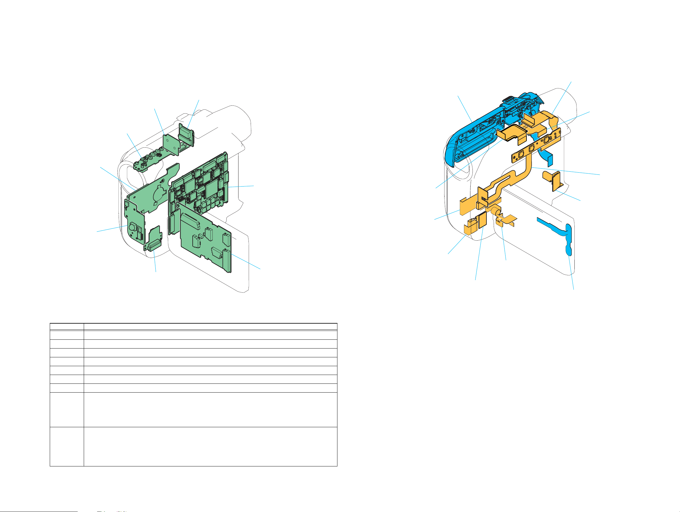
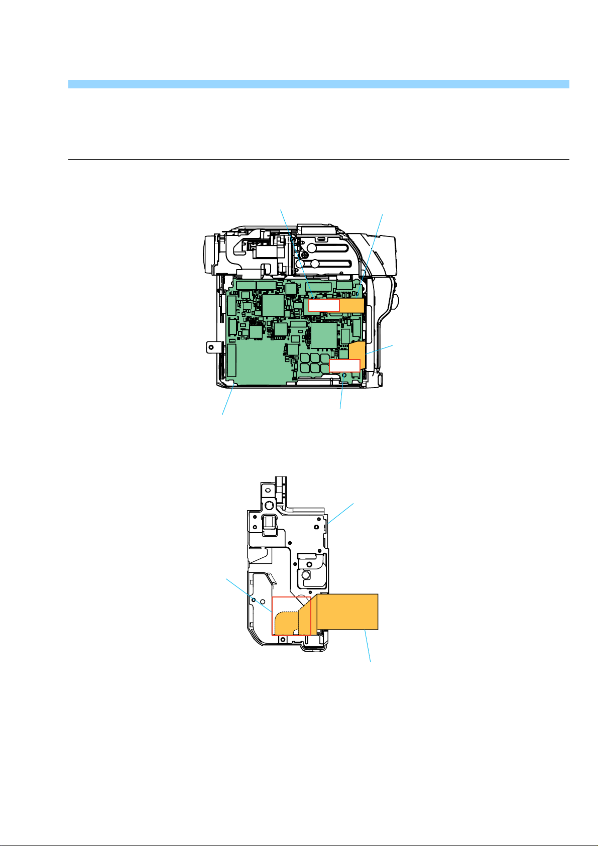
2-5. CIRCUIT BOARDS LOCATION
Non Cradle model: DCR-HC17E/HC19E/HC21/HC21E
Cradle model: DCR-HC22E/HC32/HC32E/HC33/HC33E
Non MS model: DCR-HC17E/HC19E/HC21/HC21E/HC22E
MS model: DCR-HC32/HC32E/HC33/HC33E
CD-533
JK-278
MS-249
2-6. FLEXIBLE BOARDS LOCATION
Non Cradle model: DCR-HC17E/HC19E/HC21/HC21E
Cradle model: DCR-HC22E/HC32/HC32E/HC33/HC33E
LB-109
VC-376 (Non MS model)/
VC-377 (MS model)
SI-042
PD-237
CR-050
(Cradle model)
Board Name Function
CD-533 CCD IMAGER
CR-050 CRADLE TERMINAL
JK-278 JACK
LB-109 EVF, EVF BACKLIGHT
MS-249 MS CONNECTOR
PD-237 LCD DRIVE, BACKLIGHT DRIVE
SI-042 REMOTE COMMANDER RECEIVER, PITCH/YAW SENSOR
VC-376 A/D CONVERTER, TIMING GENERATOR, LENS DRIVE, EVR,
DV SIGNAL PROCESS, DV INTERF ACE, REC/PB AMP, VIDEO OUT, AUDIO I/O
EVF DRIVE, CAMERA/MECHA CONTROL, SERVO, HI CONTROL, DC IN,
DC/DC CONVERTER, CONNECTOR
VC-377 A/D CONVERTER, TIMING GENERATOR, LENS DRIVE, VIDEO/AUDIO DSP,
DS/HI CONTROL, FLASH, SDRAM, DV SIGNAL PROCESS, DV INTERFACE,
REC/PB AMP, VIDEO, AUDIO I/O, EVF DRIVE, CAMERA/MECHA CONTROL,
SERVO, HI CONTROL, DC IN, DC/DC CONVERTER, CONNECTOR
DCR-HC17E/HC19E/HC21/HC21E/HC22E/HC32/HC32E/HC33/HC33E
2-9 2-10E
HELP
Sheet attachment positions and procedures of processing the flexible boards/harnesses are shown.
VC-376/VC-377 board
Tape (A)
FP-181 flexible board
FP-180 flexible board
Tape (A)
Tape (BT)
BT panel assy
FP-180 flexible board
DCR-HC17E/HC19E/HC21/HC21E/HC22E/HC32/HC32E/HC33/HC33E
HELP
NON MS model
Link
Link
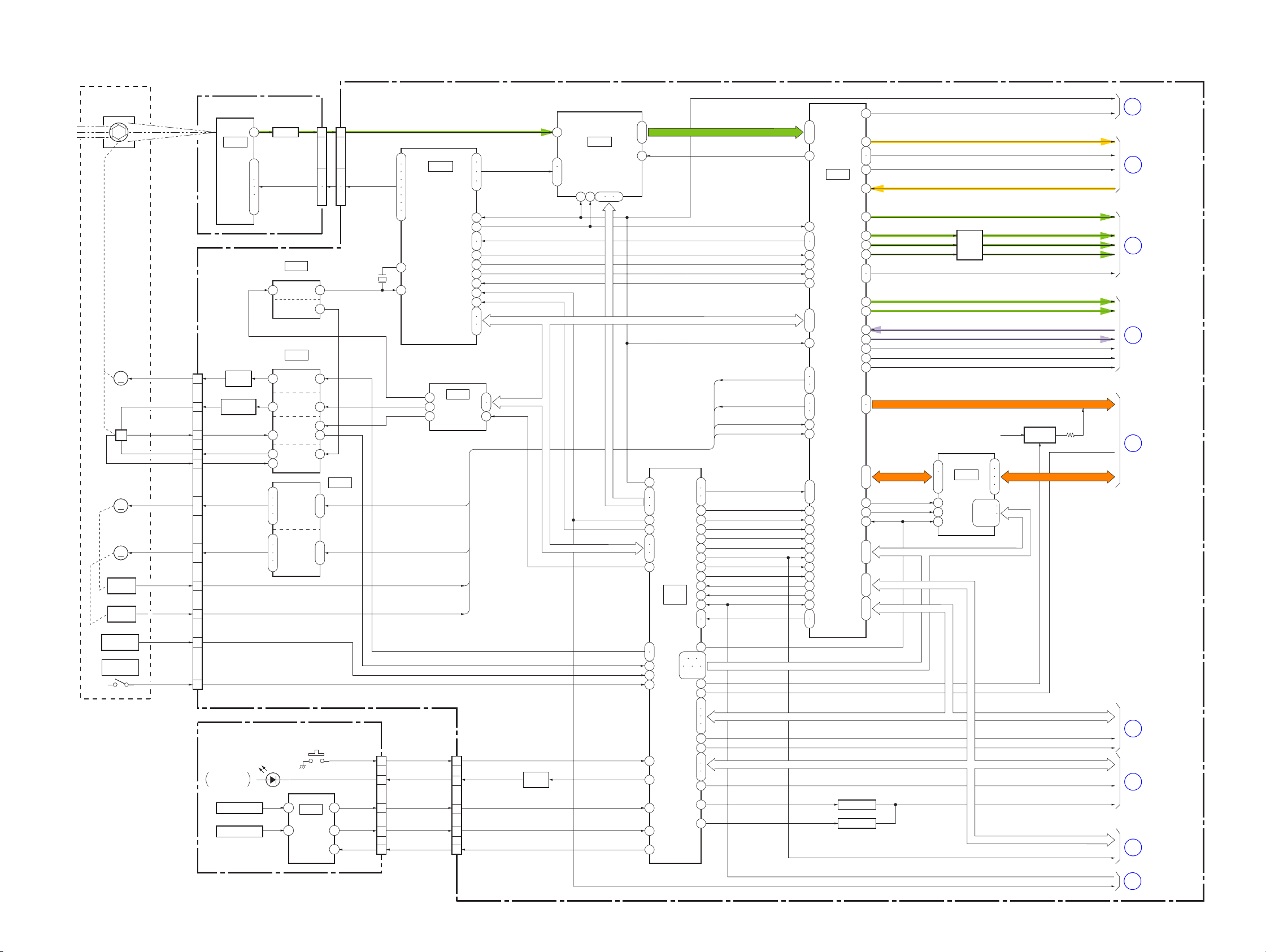
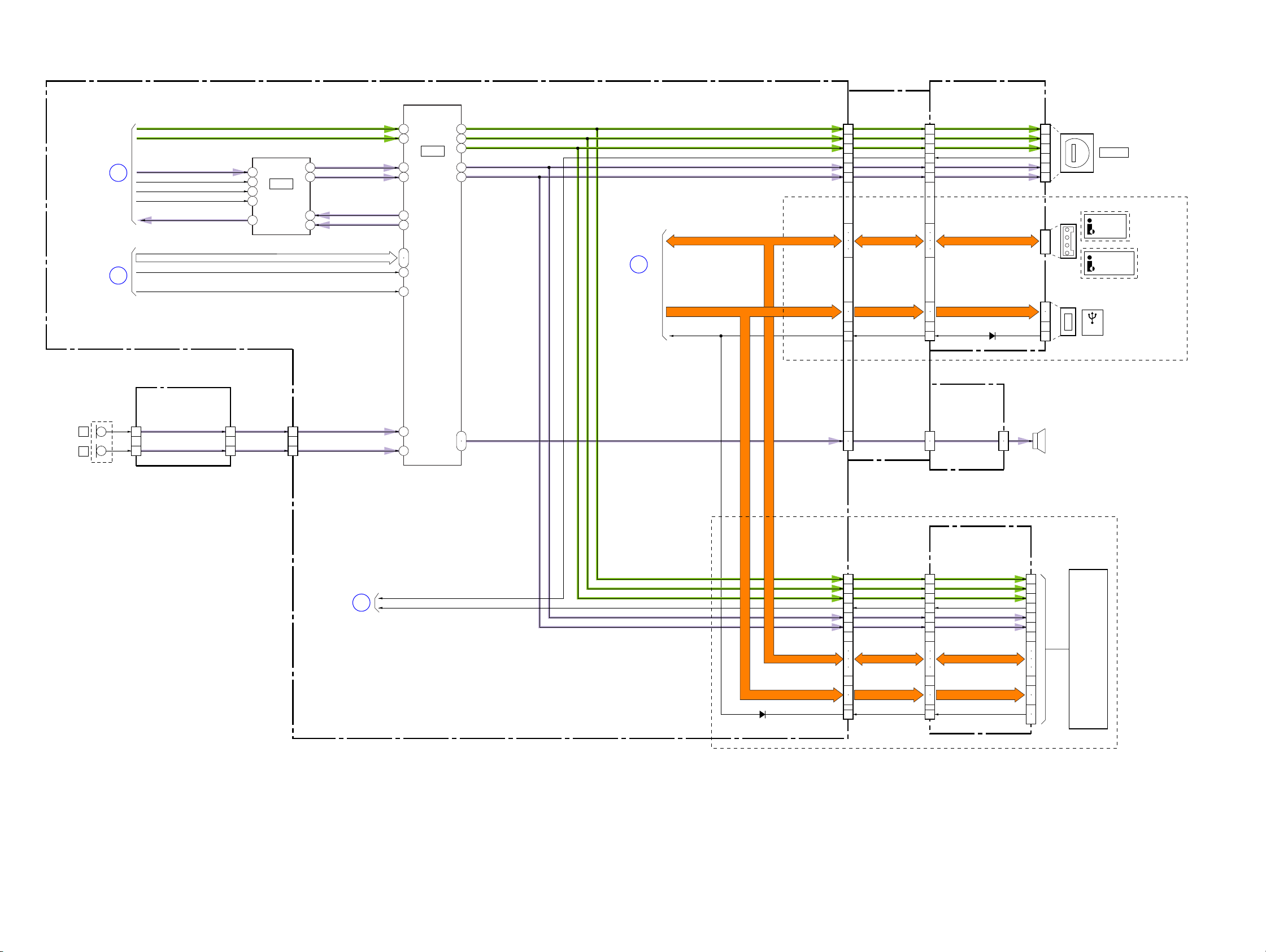
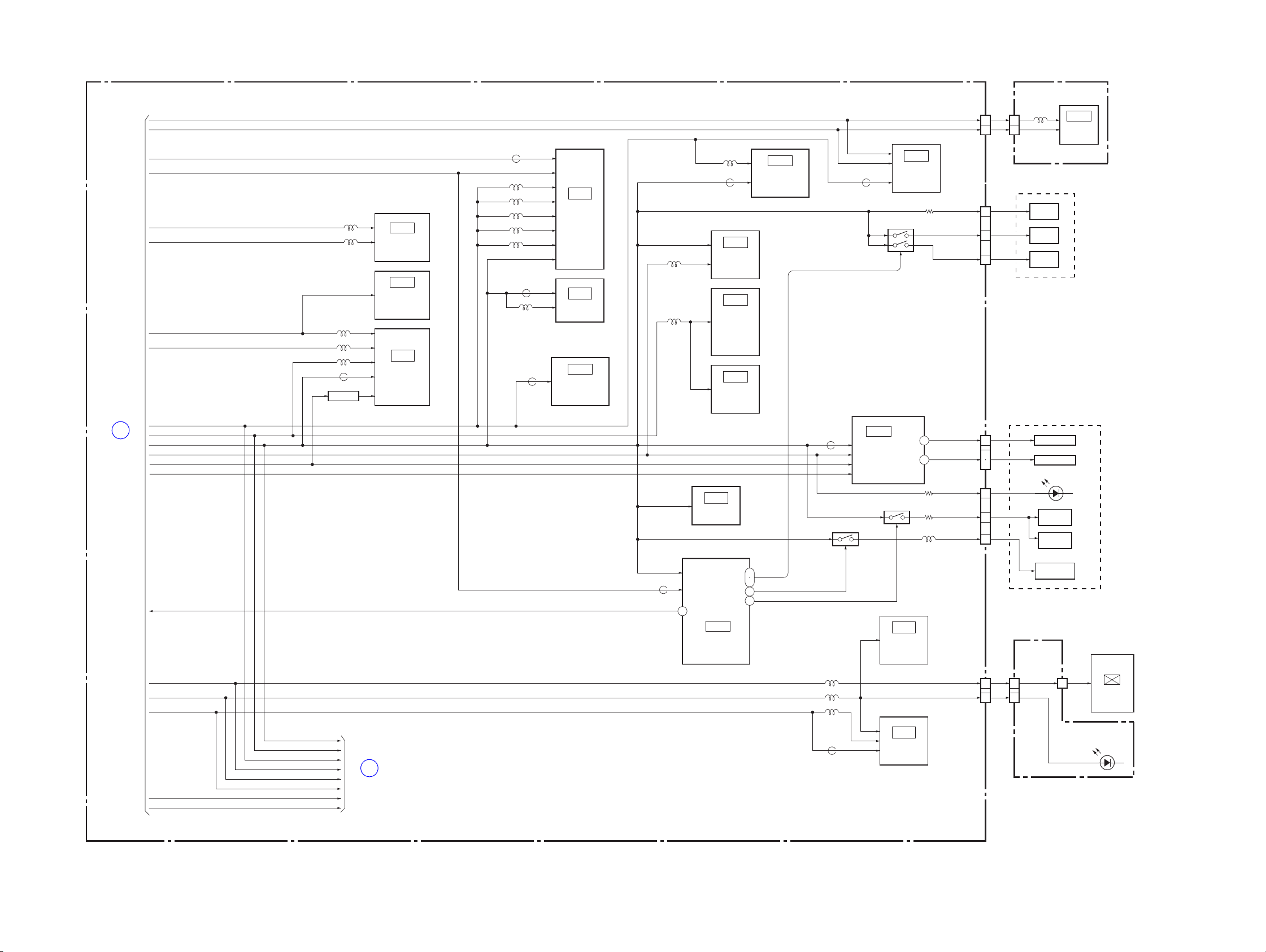
3. BLOCK DIAGRAMS
OVERALL BLOCK DIAGRAM (1/5)
OVERALL BLOCK DIAGRAM (1/5)
OVERALL BLOCK DIAGRAM (2/5)
OVERALL BLOCK DIAGRAM (2/5)
OVERALL BLOCK DIAGRAM (3/5)
OVERALL BLOCK DIAGRAM (3/5)
OVERALL BLOCK DIAGRAM (4/5)
OVERALL BLOCK DIAGRAM (4/5)
MS model
Link
Link
OVERALL BLOCK DIAGRAM (1/6)
OVERALL BLOCK DIAGRAM (1/6)
OVERALL BLOCK DIAGRAM (2/6)
OVERALL BLOCK DIAGRAM (2/6)
OVERALL BLOCK DIAGRAM (3/6)
OVERALL BLOCK DIAGRAM (3/6)
OVERALL BLOCK DIAGRAM (5/5)
OVERALL BLOCK DIAGRAM (5/5)
POWER BLOCK DIAGRAM (1/3)
POWER BLOCK DIAGRAM (1/3)
POWER BLOCK DIAGRAM (2/3)
POWER BLOCK DIAGRAM (2/3)
POWER BLOCK DIAGRAM (3/3)
POWER BLOCK DIAGRAM (3/3)
OVERALL BLOCK DIAGRAM (6/6)
OVERALL BLOCK DIAGRAM (6/6)
POWER BLOCK DIAGRAM (1/3)
POWER BLOCK DIAGRAM (1/3)
POWER BLOCK DIAGRAM (2/3)
POWER BLOCK DIAGRAM (2/3)
OVERALL BLOCK DIAGRAM (4/6)
OVERALL BLOCK DIAGRAM (4/6)
OVERALL BLOCK DIAGRAM (5/6)
OVERALL BLOCK DIAGRAM (5/6)
NON MS model: DCR-HC17E/HC19E/HC21/HC21E/HC22E
MS model: DCR-HC32/HC32E/HC33/HC33E
DCR-HC17E/HC19E/HC21/HC21E/HC22E/HC32/HC32E/HC33/HC33E
POWER BLOCK DIAGRAM (3/3)
POWER BLOCK DIAGRAM (3/3)
3. BLOCK DIAGRAMS
3-1. BLOCK DIAGRAMS (NON MS model)
3-1-1. OVERALL BLOCK DIAGRAM (1/5) (NON MS model)
LENS BLOCK
IRIS
(SHUTTER)
IRIS
METER
M
H
FOCUS
MOTOR
M
ZOOM
MOTOR
M
FOCUS
SENSOR
ZOOM
SENSOR
LENS TEMP
SENSOR
NIGHTSHOT
PLUS
A : VIDEO SIGNAL
A : AUDIO SIGNAL
I DRIVE (-)
I BIAS (-)
I HALL (-)
I BIAS (+)
I HALL (+)
FC A, FC XA,
FC B, FC XB
ZM A, ZM XA,
ZM B, ZM XB
FC SENS OUT
ZM SENS OUT
THERMO OUT
NightShot Vcc
12
8
9
6
7
1
ı
4
24
ı
27
21
16
17
19
05
A : VIDEO/AUDIO SIGNAL
A : VIDEO/AUDIO/SERVO SIGNAL
CD-533 BOARD
7
IC101
CCD
IMAGER
1
ı
4
9
10
12
ı
13
Q3101
CN3101
IRIS
DRIVE
Q3103
HALL GAIN
CONTROL
SI-042 BOARD (1/3)
D601
IR EMITTER/
NIGHTSHOT
SE601
PITCH SENSOR
SE602
YAW SENSOR
CN101
Q101
BUFFER
V1 – V4, RG,
VSHT, H1, H2
IC3103
(2/12)
XTAL AMP
HALL REG
IC3102
(2/12)
8
IRIS DRIVE
14
HALL GAIN
HALL AMP
5 7
1 3
HALL BIAS
2
2
FOCUS
4
MOTOR
21
DRIVE
23
5
ZOOM
7
MOTOR
17
DRIVE
19
(LENS COVER OPEN)
8
PITCH/YAW
SENSOR
12
10
12
12
13
16
S601
IC602
AMP
VC-376 BOARD (1/5)
CN3002
3
14
12
5
ı
ı
9
8
7
10
ı
ı
4
13
FREQ AMPOUT
75
1
6
IC3101
(2/12)
9
ı
ı
2
18
19
X3001
36MHz
LD EN0, LD DIR0A, LD DIR0B
LD EN1, LD DIR1A, LD DIR1B
CN603
(1/3)
13
11
( ) : Number in parenthesis ( ) indicates the division number of schematic diagram where the component is located.
141
18
21
22
25
26
28
31
33
5
4
FREQ TUNE
HALL GAIN
HALL OFFSET
XSHUTTER OPEN
5
3
VST C RESET
2
CCD OUT
GENERATOR
1
2
3 8
NS LED K
PITCH AD
YAW AD
IC3001
TIMING
(1/12)
IC9201
EVR
(D/A CONVERTER)
(2/12)
FC RST
ZM RST
6
8
14
16
17
30
1
CLPDM, PBLK,
15
16
40
12
44
45
34
41
48
36
42
39
35
38
37
CN1004
(1/3)
2
XSHP, XSHD
XRST VTR
VCK VCK
CAM DD ON
XCS TG
6
CAM SO, CAM SCK
7
Q1001
LED
DRIVE
19
21
23
IC3002
S/H, AGC,
A/D CONVERTER
ı
(1/12)
1643
46 47 48
CAM DD ON
CAM SI, CAM SO, CAM SCK
IRIS PWM, IRIS COM
LENS TEMP AD
XSHUTTER OPEN
VST C RESET
2
ı
11
FE CLPOB
20
CS CH, CH SO, CH SCK
XRST VTR
100
62
XCS TG
IR ON
YAW AD
73
71
173
20
77
78
75
59
94
95
128
127
187
205
194
129
130
40
CS CH, CH SO, CH SCK
DA STRB
HALL AD
XNS SW
PITCH AD
IC8601
(1/2)
CAMERA/
MECHA
CONTROL
(7/12)
22 24 25
33 32
52 – 45
AD0 – AD9
TG AHD, TG AVD
TG ZSG1
TG ZV1
TG ID
TG VGAT
CAM SI, CAM SO, CAM SCKCAM SI, CAM SO, CAM SCK
XRST VTR
LD EN0, LD DIR0A, LD DIR0B
LD EN1, LD DIR1A, LD DIR1B
FC RST
ZM RST
23
179
178
97
161
208
132
163
164
155
215
201
204
214
203
68
18
131
113
61
80
82
83
38
39
70
69
67
43
98
202
FRRV, TRRV, TRRT
XCS IC 6001
XCS IC 6001-2
XIRQ IC 6001
XUSB EN
DRP
SWP
XCS VFD
XCS SFD
LINEOUT VD
VREF
OSD V
VFO VD, VFO OE
XCS IC 6002
D24A00 – D31A07, DXXA08, DXXA09, ALE, WRX, RDX
USB ON
USB DET
XCS VD, VD SI, VD SO, VD SCK VD SI, VD SO, VD SCK
VSP SI, VSP SO, XVSP SCK
MERODY ENV
MERODY CARR
199
208
209
216
214
215
212
213
194
196
190
11
12
14
15
180
178
189
193
197
129
161
162
187
188
182
181
192
42
43
ı
3
4
ı
5
6
8
9
ı
IC6001
DV SIGNAL
PROCESS
(3/12)
MODULATOR
MODULATOR
Q8602
Q8601
77
75
76
78
96
116
121
123
119
130
131
110
113
63
64
68
67
69
126
127
154
157
159
143
177
164
176
184
186
18
20
Q6001
BUFFER
USB D± USB D±
Q6003
USB 3.1V
24
IC6002
LBUS0-3
ı
LCKO
TRCKO
XCS IC 6002
D24A00 – D31A07, DXXA08, DXXA09, ALE, WRX, RDX
ı
ı
VSP SI, VSP SO, XVSP SCK
ı
XCS VD, VD SO, VD SCK
26
ı
DV INTERFACE
28
62
19
78
(3/12)
2 – 4
6 – 9 11
75 – 77
52
51
48
47
PULL UP
XRST VTR
RECDT
RECA1,2
RECCK
PANEL R
PANEL G
PANEL B
PANEL HD, PANEL VD
IC 6001 Y OUT
IC 6001 C OUT
DATA TO SFD
DATA FROM SFD
SFD BCK
SFD LRCK
SFD FCK
USB
USB DET
TPA±, TPB±
VSP SO, XVSP SCK
VSP SO, XVSP SCK
OSD V
CAM DD ON
SPCK
RF IN
BW Y
USB D+
XCS LCD
XCS EVF
XCS AU1
BEEP
SWP
OVERALL1 (2/5)
1
OVERALL1 (2/5)
2
(PAGE 3-4)
OVERALL1 (3/5)
3
(PAGE 3-5)
OVERALL1 (4/5)
4
(PAGE 3-7)
OVERALL1 (4/5)
5
(PAGE 3-8)
OVERALL1 (3/5)
6
(PAGE 3-5)
OVERALL1 (4/5)
7
(PAGE 3-7)
OVERALL1 (2/5)
8
(PAGE 3-3)
OVERALL1 (5/5)
9
(PAGE 3-10)
(PAGE 3-3)
DCR-HC17E/HC19E/HC21/HC21E/HC22E/HC32/HC32E/HC33/HC33E
3-1 3-2
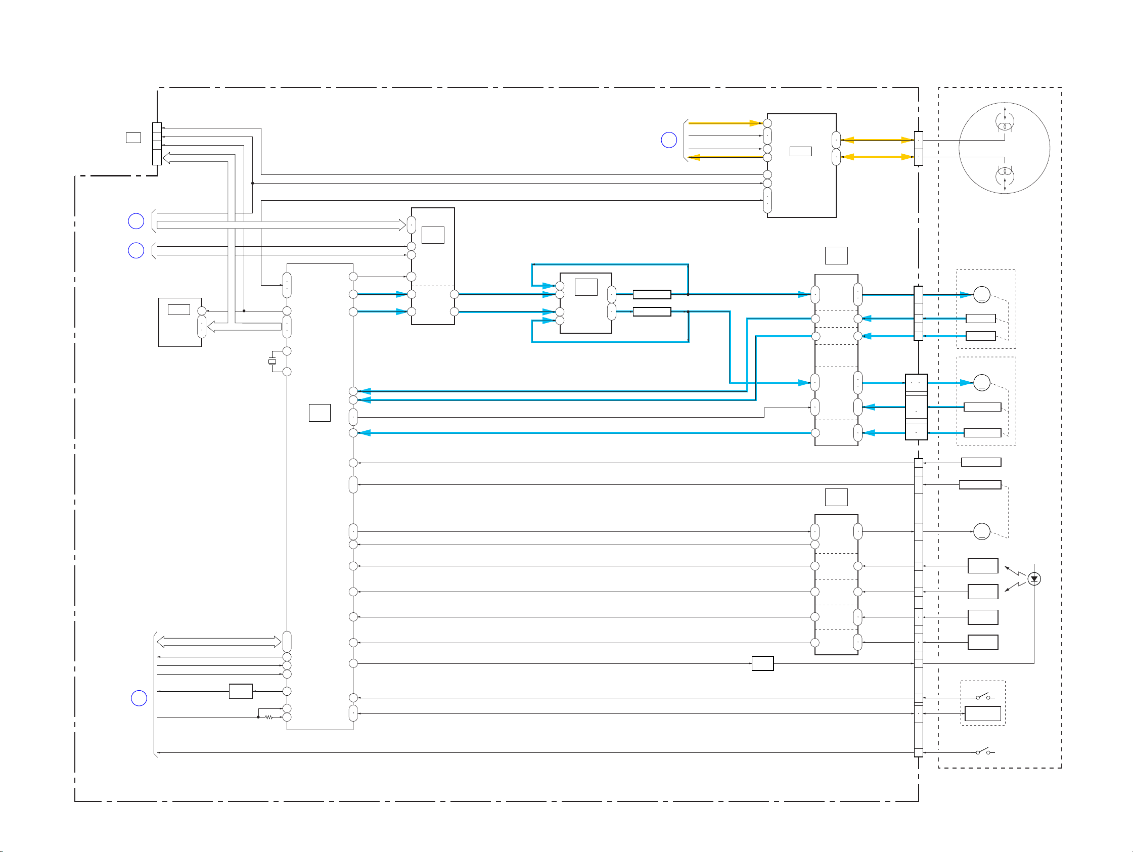
3-1-2. OVERALL BLOCK DIAGRAM (2/5) (NON MS model)
VC-376 BOARD (2/5)
( ) : Number in parenthesis ( ) indicates the division number of schematic diagram where the component is located.
Z MECHA DECK
(MDX-Z210)
VIDEO HEAD
(FOR CHECK)
OVERALL1 (1/5)
(PAGE 3-2)
OVERALL1 (1/5)
(PAGE 3-2)
OVERALL1 (5/5)
(PAGE 3-9)
CPC
8
1
10
CN1007
RF MON
1
SWP
2
XCS EEP
4
7
ı
EEP SI, EEPSO, EEP SCK
5
SWP
XRST VTR
Q8607
LED
DRIVE
XCS EEP
X8601
20MHz
IC8602
64k EEPROM
IC 8001 SI, IC 8001 SO. IC 8001 SCK. XCS IC 8001
SYS V
ZOOM VR AD
XCRADLE IN
XEASY MODE LED
XSYS RST
(7/12)
1
2
5
EEP SI, EEPSO, EEP SCK
6
CONT1, SW PS, ALL PS
172
29
28
10
87
86
84
3
1
IC8601
(2/2)
MECHA
CONTROL
(7/12)
63
ı
66
181
135
189
169
8
9
RECDT
OVERALL1 (1/5)
(PAGE 3-2)
VSP SO, XVSP SCKVSP SO, XVSP SCK
XRST VTR
XCS IC 9001
16
DRUM PWM
88
CAP PWM
89
197
198
CAP FWD, CAP ON
166
165
CAP FG
190
DEW AD
119
106
MODE SW A – C
ı
108
LOAD, UNLOAD
15
13
LM LIM DET LM LIM DET
138
TAPE END
31
TAPE TOP
30
TREEL FG
192
SREEL FG
193
TAPE LED ON
180
REC PROOF
110
195
CHIME SDA, SCK
196
38
36
IC9001
(3/3)
34
35
37
44
41
(8/12)
SERIAL
INTERFACE
LPF
45
43
DRUM
ERROR
CAP
ERROR
DRUM FG
DRUM PG
7
21
24
8
IC2201
(1/2)
DRUM/
CAPSTAN
PWM DRIVE
(11/12)
77
78
75
76
Q2208
SWITCHING
SWITCHING
Q2207
SPCKSPCK
RECA1,2
2
RECCK
RF IN
CONT1, SW PS, ALL PS
DRUM VS
RF MON
SWP
46
40
42
44
35
30
38
39
37
45
CAP FWD, CAP ON
LOAD, UNLOAD
Q9002
LED
DRIVE
REC/PB AMP
DRUM FG
DRUM PG
CAP VS
CAP FG
TAPE END
TAPE TOP
TREEL FG
SREEL FG
IC6501
(4/12)
64
67
53
50
75
77
80
32
33
31
21 20
19
29
25
10
9
3
4
IC9001
(1/3)
(8/12)
DRUM
MOTOR
DRIVE
FG AMP
PG AMP
CAPSTAN
MOTOR
DRIVE
1
FG AMP
4
IC9001
(2/3)
(8/12)
LOADING
MOTOR
DRIVE
TAPE END
DETECT
TAPE TOP
DETECT
T REEL
FG AMP
S REEL
FG AMP
CHIME SDA, CHIME SCK
XODD, YODD
XEVEN, YEVEN
63
DRUM U, V, W
65
68
52
49
74
CAP U, V, W
76
78
10
ı
15
7
8
DEW AD
MODE SW A-C
69
72
TAPE END C
TAPE TOP C
18
26
T REEL ±
27
22
S REEL ±
23
TAPE LED K
REC PROOF
FG
PG
UHE±,
VHE±,
WHE±
FG1, 2
LM ±
CN6501
CN9001
CN9003
CN9002
ODD
6
5
2
3
EVEN
M901
1
ı
6
10
9
1
11
17
ı
ı
ı
4
14
20
6
ı
10
15
22
25
5
7
ı
9
1
ı
4
20
11
26
25
22
23
18
12
14
15
DRUM MOTOR
M
DRUM FG
DRUM PG
M903
CAPSTAN MOTOR
M
HU, HV, HW
CAPSTAN FG
DEW SENSOR
S902
MODE SWITCH
M902
LOADING MOTOR
M
Q901
TAPE END
SENSOR
Q902
TAPE TOP
SENSOR
H902
T REEL
SENSOR
H901
S REEL
SENSOR
MIC902
REC PROOF
4PIN
CONNECTOR
D901
TAPE LED
05
DCR-HC17E/HC19E/HC21/HC21E/HC22E/HC32/HC32E/HC33/HC33E
3-3 3-4
S903
XCC DOWNXCC DOWN
17
CC DOWN
A : VIDEO/AUDIO/SERVO SIGNAL
A : SERVO SIGNAL

3-1-3. OVERALL BLOCK DIAGRAM (3/5) (NON MS model)
( ) : Number in parenthesis ( ) indicates the division number of schematic diagram where the component is located.
VC-376 BOARD (3/5)
OVERALL1 (1/5)
(PAGE 3-2)
OVERALL1 (1/5)
(PAGE 3-2)
OVERALL1 (5/5)
(PAGE 3-9)
3
6
11
BW Y
PANEL R
PANEL G
PANEL B
PANEL HD, PANEL VD
XCS EVF
XCS LCD
TP X
TP Y
TP SEL1
PANEL HD, PANEL VD
VD SI, VD SO, VD SCK
IC9303
EVF BACKLIGHT
CONTROL
(6/12)
PANEL HD, PANEL VD
VD SI, VD SO, VD SCKVD SI, VD SO, VD SCK
BW Y
XCS EVF
EXTDA
3
+
2
–
PANEL R
PANEL G
PANEL B
XCS LCD
TP SEL1
1
CN1006
(1/2)
TP X
TP Y
33
48
1
42
45
44
43
31
1
2
3
12
13
19
22
21
20
18
16
17
IC9301
EVF DRIVE
(6/12)
12 14 16
17 28 24
6 – 10
20
21
22
26
EVF HST,HCK1, HCK2,
BLK, STB, VCK, PCG,
REF, VST, EN, PSIG
BL ON
18
Q9303
BACKLIGHT
DRIVE
PD-237 BOARD (1/2)
CN601
(1/2)
1
2
3
PANEL HD, PANEL VD
12
13
19
22
VD SI, VD SO, VD SCK
21
20
TP X
18
TP Y
16
TP SEL1
17
EVF VR
EVF VG
EVF VB
COM CS
PANEL R
PANEL G
PANEL B
XCS LCD
CN9301
LED K
EXTDA
BL ON
LB-109 BOARD
CN301
16
15
14
18
4
ı
13
17
23
34
33
32
48
1
42
45
44
43
31
18
6
7
8
4
18
ı
9
5
1
IC602
LCD DRIVE
14 16 17
HST,HCK1, HCK2,
BLK, STB, VCK, PCG,
REF, VST, EN, PSIG
5 – 12
24 28
CN302
VR
VG
VB
COM, CS
D303
(BACKLIGHT)
20
21
22
26
RGT, PSIG, HCK1, HCK2,
WIDE, REF, HST, PCG,
XSTBY, DWN, EN, VCK, VST
17
18
16
21
19
5
ı
7
9
ı
15
20
COM, CS
TOUCH
PANEL
I/F
Q601, 602
LCD902
B/W
EVF
UNIT
R
G
B
CN605
CN603
TP TOP
TP L
TP R
TP BOT
4
5
3
23
24
2
6–9
11–14
19–22
3
5
2
6
LCD901
2.5 inch
COLOR
LCD
UNIT
TOUCH
PANEL
IC601
BACKLIGHT
CONTROL
3
+
1
2
–
05
BL 2.8V
Q606, 607,
611, 612
BACK LIGHT
DRIVE
BL –15.5V
BL 2.8V
CN608
BL H
BL FB
6
1
4
3
D901
BACKLIGHT
A : VIDEO SIGNAL
DCR-HC17E/HC19E/HC21/HC21E/HC22E/HC32/HC32E/HC33/HC33E
3-5 3-6
3-1-4. OVERALL BLOCK DIAGRAM (4/5) (NON MS model)
( ) : Number in parenthesis ( ) indicates the division number of schematic diagram where the component is located.
VC-376 BOARD (4/5)
OVERALL1 (1/5)
(PAGE 3-2)
OVERALL1 (1/5)
(PAGE 3-2)
MIC901
MICROPHONE
UNIT
L
R
4
7
IC 6001 Y OUT
IC 6001 C OUT
DATA FROM SFD
SFD BCK
SFD LRCK
SFD FCK
DATA TO SFD
XCS AU1
BEEP
SI-042 BOARD (2/3)
CN601
INT MIC L
1
INT MIC R
3
CN603
(2/3)
9
7
9
12
10
11
CONVERTER
8
INT MIC L
INT MIC R
IC6702
A/D, D/A
(5/12)
10
12
15
16
3
2
CN1004
(2/3)
PBIN L
PBIN R
RECOUT L
RECOUT R
VSP SO, XVSP SCKVSP SO, XVSP SCK
17
15
24
23
26
25
21
20
19
47
37
38
IC6701
VIDEO OUT,
AUDIO I/O
(5/12)
7
12
9
41
45
1
3
S Y I/O
S C I/O
VIDEO I/O
AUDIO L I/O
AUDIO R I/O
5
OVERALL1 (1/5)
(PAGE 3-2)
S Y
S C
VIDEO I/O
MULTI JACK IN
AUDIO L I/O
AUDIO R I/O
TPA±, TPB± TPA, NTPA, TPB, NTPB
USB D±USB D±
USB DET
CN1008
(1/2)
FP-182 FLEXIBLE
BOARD (1/2)
8
6
14
15
10
12
18
19
21
22
25
24
26
43
44
JK-278 BOARD (1/2)
CN704
(1/2)
8
6
14
15
10
12
17
18
TPA, NTPA, TPB, NTPB
20
21
24
23
25
MS-249 BOARD
(1/2)
CN501
(1/2)
12
13
USB D±
SP±SP±SP±
VIDEO IN/OUT
JACK AD
AUDIO L
AUDIO R
D703
CN502
1
2
S-Y
S-C
VCCUSB DETUSB DET
CN701
CN703
CN702
SP901
SPEAKER
10
5
9
7
1
6
A/V OUT
DCR-HC17E/HC19E
1
ı
4
(DV OUT)
(DV IN/OUT)
DCR-HC21/HC21E
3
2
1
(USB)
NON CRADLE model
05
OVERALL1 (5/5)
(PAGE 3-9)
12
A : VIDEO SIGNAL
A : AUDIO SIGNAL
A : VIDEO/AUDIO SIGNAL
MULTI JACK IN
MULTI JACK IN CRADLE
MULTI JACK IN
TPA, NTPA, TPB, NTPB
D1016
S Y I/O
S C I/O
VIDEO I/O
AUDIO L I/O
AUDIO R I/O
USB D±
CN1003
(1/2)
CRADLE model
CR-050 BOARD (1/2)
CN001
(1/2)
18
10
9
7
6
4
3
34
3220
4012
3913
3616
3814
42
43
45
46
48
49
502
S Y I/O
S C I/O
VIDEO I/O
MULTI JACK IN
AUDIO L I/O
AUDIO R I/O
TPA, NTPA, TPB, NTPB
USB D±
USB DETUSB DET
CN002
(1/2)
9
13
10
8
18
14
31
29
33
35
32
34
24
26
CRADLE
(1/2)
CRADLE model: DCR-HC22E
NON CRADLE model: DCR-HC17E/HC19E
/HC21/HC21E
DCR-HC17E/HC19E/HC21/HC21E/HC22E/HC32/HC32E/HC33/HC33E
3-7 3-8
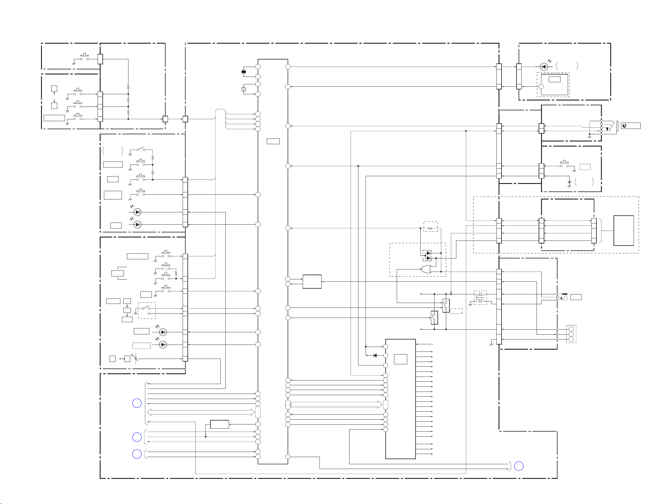
3-1-5. OVERALL BLOCK DIAGRAM (5/5) (NON MS model)
( ) : Number in parenthesis ( ) indicates the division number of schematic diagram where the component is located.
FP-186 FLEXIBLE BOARD
S101
(PANEL REVERSE)
CONTROL KEY BLOCK
(ZOOM)
S001
START/STOP
(SB9000)
W
S003
S002
T
3
4
5
4
3
CN609
CN602
PD-237 BOARD (2/2)
PANEL REVERSE
2ND ZOOM (W)
2ND ZOOM (T)
2ND S/S SW
KEY AD1 KEY AD1
FP-187 FLEXIBLE BOARD
S004
PANEL
OPEN/CLOSE
S003
BACK LIGHT
S002
EASY
S001
DSPL/
BATT INFO
D001
(EASY)
D004
CHG
CONTROL KEY BLOCK (SS10300)
S004
START/STOP
S003
(PHOTO FREEZE)
PHOTO
POWER
RV001
W T
(ZOOM)
OVERALL1 (2/5)
(PAGE 3-3)
OVERALL1 (3/5)
(PAGE 3-5)
OVERALL1 (4/5)
(PAGE 3-7)
05
DCR-HC17E/HC19E/HC21/HC21E/HC22E/HC32/HC32E/HC33/HC33E
OFF
ON
MODE
S002
(PHOTO REC)
S001
EJECT
D001
CAMERA
D002
PLAY/EDIT
10
11
12
VC-376 BOARD (5/5)
X8002
10MHz
X8001
32.768kHz
CN601
(2/2)
6
KEY AD3 KEY AD3
BATT INFO XBATT INFO SW
XEASY LED
XCHARGE LED
ZOOM VR AD
XEASY MODE LED
XCC DOWN
SYS V
XSYS RST
IC 8001 SI, IC 8001 SO. IC 8001 SCK. XCS IC 8001
XCRADLE IN
TP X
TP Y
TP SEL1
MULTI JACK IN
MULTI JACK IN CRADLE
6
2
3
4
7
1
10
14
8
7
3
5
12
CN1006
(2/2)
CN1002
CN1001
KEY AD0
KEY AD2
XEJECT SW
XPOWER SW
XMODE SW
XCAM LED
XVTR LED
ZOOM VR
Q8002
TP SELECT
SWITCH
KEY AD0
KEY AD1
KEY AD2
KEY AD3
3-9 3-10
TP SEL2
28
29
51
52
59
60
61
65
3
12
4
1
2
11
9
5
32
47
23
ı
26
48
70
71
34
68
69
IC8001
HI CONTROL
(9/12)
10
41
72
73
74
42
43
37
38
39
40
8
46
20
21
35
49
19
XLANC JACK IN
XRESET
BATT/XEXT
Q8001
BATTERY
CHARGE
DETECTOR
FAST CHARGE
INIT CHARGE ON
HI EVER SO, HI EVER SCK
LANC IN
LANC OUT
XLANC PWR ON
XLANC ON
BATT IN
VTR DD ON
XCS DD
XRESET
LANC SIG
CAM DD ON
LI 3V
CRADLE model
DOUBLE
INSERTION DETECT
BATT UNREG
45
46
IC2201
(2/2)
51
DC CONTROL,
RESET,
LANC DRIVE
57
(11/12)
54
56
55
52
14
15
5031
44
13
5
NON CRADLE model
R2010
D2006
Q2005
ACV UNREG
Q2003,
2004
CRADLE
ACV UNREG
D 1.5V
MT 5V
NS 2.8V
RP 2.8V
A 2.8V
D 2.8V
AU 2.8V
EP 2.8V
A 4.6V
AU 4.6V
EP 4.6V
RP 4.6V
CAM 15V
IC 9001 13.5V
EP 8.5V
BL -15.5V
CAM -7.5V
USB 3.1V
EVER 3.0V
VOUT
LANC DC
Q2001,
2002,
Q2006
model
CN1004
XF TALLY LED
SIRCS SIG
CN1008
XLANC JACK IN
LANC SIG
XRESET
LI 3V
CN1003
LANC SIG
XCRADLE IN
CN2001
LF2001
CAM DD ON
(3/3)
17
15
FP-182 FLEXIBLE
BOARD (2/2)
(2/2)
(2/2)
2
4
3
2
42
24
51
ı
42
26
FP-180 FLEXIBLE BOARD
BATT/XEXT
30
BATT SIG
9
24
ACV UNREG
ı
29
16
ACV GND
ı
21
1
BATT UNREG
ı
6
10
BATT GND
ı
15
OSD V
9
SI-042 BOARD (3/3)
CN603
(3/3)
IC601
REMOTE
4
COMMANDER
RECEIVER
JK-278 BOARD (2/2)
CN704
(2/2)
3
2
MS-249 BOARD (2/2)
CN501
(2/2)
11
1041
CR-050 BOARD (2/2)
CN001
(2/2)
28
2527
1
ı
10
26 21
OVERALL1 (1/5)
(PAGE 3-2)
D602
CAMERA
RECORDING
DCR-HC19E/HC21/
HC21E/HC22E
XLANC JACK IN
LANC SIG
S501
RESET
BT501
LITHIUM
BATTERY
CN002
LANC SIG
XCRADLE IN
ACV UNREGACV UNREG
BATT/XEXTBATT/XEXT
(2/2)
25
19
1
ı
4
CRADLE
(2/2)
CRADLE model
J001
DC IN
+
BH001
C
BATTERY
TERMINAL
–
CRADLE model: DCR-HC22E
NON CRADLE model: DCR-HC17E/HC19E
/HC21/HC21E
J701
(LANC)
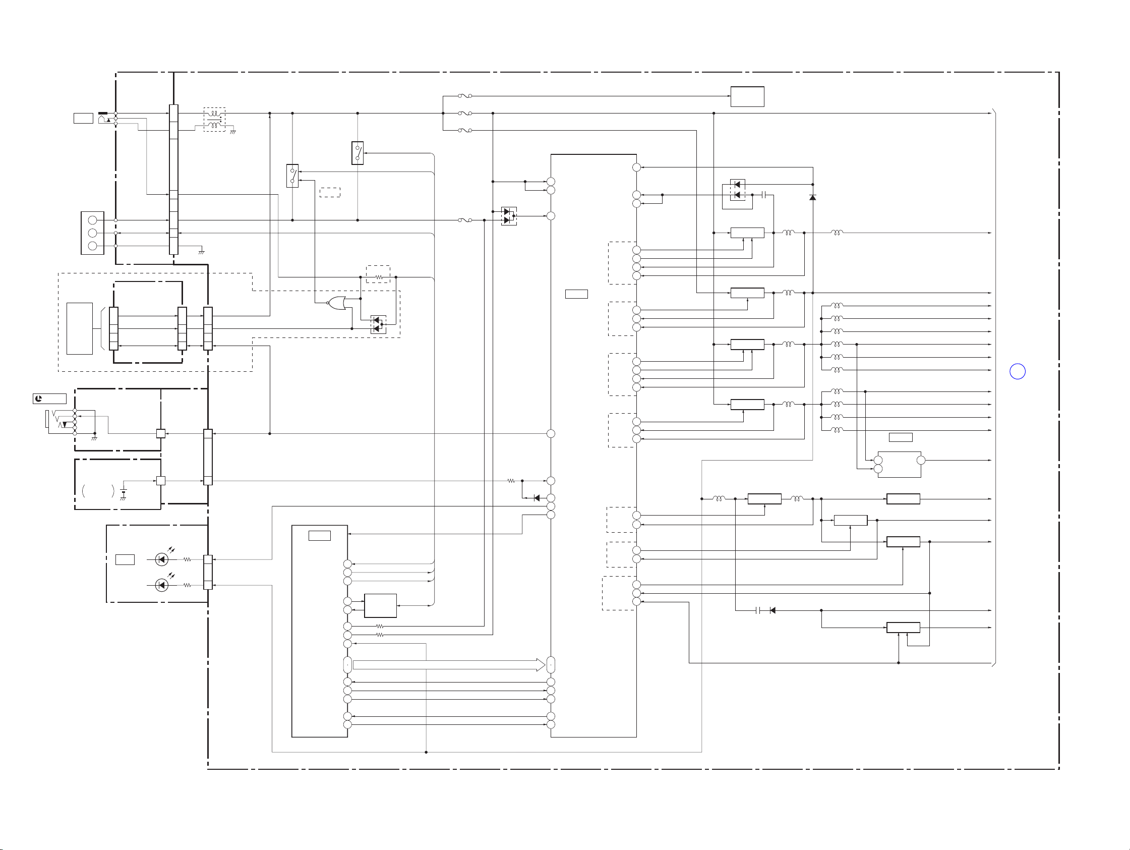
3-1-6. POWER BLOCK DIAGRAM (1/3) (NON MS model)
( ) : Number in parenthesis ( ) indicates the division number of schematic diagram where the component is located.
FP-180
FLEXIBLE
BOARD
ACV UNREG
BH001
BATTERY
TERMINAL
J001
DC IN
+
C
−
CR-050 BOARD
CN002
1
ACV UNREG ACV UNREG
ı
4
CRADLE
BATT/XEXT BATT/XEXT
LANC DC LANC DC
27
CRADLE model
J701
(LANC)
JK-278 BOARD
LANC DC LANC DC
MS-249 BOARD
BT501
LITHIUM
BATTERY
CN704
CN501
FP-187 FLEXIBLE BOARD
D004
CHG
D001
(EASY)
CRADLE model: DCR-HC22E
NON CRADLE model: DCR-HC17E/HC19E
/HC21/HC21E
VC-376 BOARD (1/3)
CN2001
24
ı
29
16
ı
21
30
1
ı
6
9
10
ı
15
LF2001
Q2003,
Q2001,
BATT/XEXT
BATT UNREG
BATT SIG BATT SIG
2002,
Q2006
CRADLE
model
NON CRADLE model
CN001
1
ı
10
2621
30
FP-182
FLEXIBLE
BOARD
4
10 41
CN1003
51
ı
42
26
22
CN1008
4
LI 3V
CN1002
CHARGE LED VDD
8
EASY LED VDD
5
Q2005
DOUBLE
INSERTION DETECT
IC8001
HI CONTROL
(9/12)
BATT/EXT
FAST CHARGE
INIT CHARGE
IB SO
IB SI
ACV SENSE
HI EVER SO
HI EVER SCK
BATT IN
VTR DD ON
XCS DD
XLANC POWER ON
XLANC ON
74
37
38
42
43
DETECTOR
54BATT SENSE
55
55VTR DD SENSE
20
21
31
35
49
8
46
2004
INIT CHARGE ON
R2010
D2006
INIT CHARGE ON
Q8001
BATTERY
CHARGE
FAST CHARGE
BATT/XEXT
EVER 3.0V
VOUT
BATT/XEXT
FAST CHARGE
BATT SIG
F002
F003
F001
D2201
F004
VTR UNREG
BATT UNREG
HI EVER SO, HI EVER SCK
BATT IN
VTR DD ON
XCS DD
XLANC PWR ON
XLANC ON
D2202
61
VCC1
60
VCC3
49
VCC2
IC2201
DC CONTROL,
RESET,
LANC DRIVE,
DRUM/CAPSTAN
PWM DRIVE
(11/12)
58
VOUT4
VBATT
45
VOUT3
46
47
VOUT2
48
VOUT1
DIN
14
15
CLK
50
OUTC1
44
CTL1
13
LD
55
WAKEUP
52
XCTL2
Q2207, 2208
L2207
CAPSTAN/
DRUM
SWITCHING
D2204
Q2201, 2203
SWITCHING
Q2204
SWITCHING
Q2202, 2205
SWITCHING
Q2206
SWITCHING
Q2209
SWITCHING
D2205
D2203
L2201 L2209
L2202
L2210
L2211
L2212
L2203
L2204
L2208
L2213
L2214
L2215
L2216
L2217
L2218
L2219
Q2212
8.5V REG
IC2202
3.1V REG (11/12)
VOUTVIN
5 4
1
ON/OFF
Q2210
13.5V REG
Q2211
15V REG
Q2213, 2214
-7.5V REG
IC 9001 13.5V
CAM DD ON
C/D UNREG
VTR UNREG VTR UNREG
MT/15.5/BL UNREG
62VB
63VCCO1
67VCCO2
OUT1-1
64
66
OUT1-2
65
VS1
12
IN1
68
OUT2
69
VS2
11
IN2
70
OUT3-1
72
OUT3-2
71
VS3
10
IN3
73
OUT4
74
VS4
9
IN4
79
OUT7
6
IN7
79
VCONT5
2
VOUT5
3
VCONT6
4
VOUT6
REG6CTL
5
CAM DD ON
D 1.5V
MT 5V
NS 2.8V
RP 2.8V
A 2.8V
D 2.8V
AU 2.8V
EP 2.8V
A 4.6V
AU 4.6V
EP 4.6V
RP 4.6V
USB 3.1V
EP 8.5V
CAM 15V
BL -15.5V
CAM -7.5V
A
POWER1 (2/3)
(PAGE 3-13)
05
DCR-HC17E/HC19E/HC21/HC21E/HC22E/HC32/HC32E/HC33/HC33E
MT 5VMT 5V
3-11 3-12
3-1-7. POWER BLOCK DIAGRAM (2/3) (NON MS model)
( ) : Number in parenthesis ( ) indicates the division number of schematic diagram where the component is located.
VC-376 BOARD (2/3)
CAM 15V
CAM -7.5V
USB 3.1V
D 1.5V
RP 2.8V
RP 4.6V
AU 2.8V
AU 4.6V
A 2.8V
A
POWER1 (1/3)
(PAGE 3-12)
A 4.6V
D 2.8V
MT 5V
VTR UNREG
IC 9001 13.5V
CAM DD ON
EP 8.5V
EP 4.6V
EP 2.8V
L6501
L6502
L6701
L6702
L6704
FB6701
Q6701
3.2V REG
IC6501
REC/PB AMP
(4/12)
IC6702
A/D, D/A
CONVERTER
(5/12)
IC6701
VIDEO OUT,
AUDIO I/O
(5/12)
FB6001
L6002
L6003
L6004
L6005
L6006
FB6002
L6009
FB9201
IC6001
DV SIGNAL
PROCESS
(3/12)
IC6002
DV INTERFACE
(3/12)
IC9201
EVR
(D/A CONVERTER)
(2/12)
A 2.8V
A 4.6V
D 2.8V
MT 5V
VTR UNREG
IC 9001 13.5V
D 1.5V
EP 8.5V
EP 4.6V
EP 2.8V
CAM 15V
CAM -7.5V
A 2.8V
D 2.8V
L3101
L3102
FB8602
IC8602
64k EEPROM
CHIME PWR CONT
XREEL HALL ON
173
CAM DD ON
CAMERA/MECHA
CONTROL
L3001
IC3101
FOCUS/ZOOM
MOTOR DRIVE
(2/12)
IC3102
IRIS DRIVE,
HALL BIAS/
HALL GAIN
CONTROL,
HALL AMP
(2/12)
IC3103
HALL REG,
XTAL AMP
(2/12)
(7/12)
ZM RST LED
FC RST LED
IC8601
(7/12)
IC3002
S/H, AGC,
A/D CONVERTER
55
57
133
153
(1/12)
FB3003FB3004
ZM RST LED, FC RST LED
FB9001
Q8603 - 8605
L9303
L9302
L9301
IC9001
DRUM/
CAPSTAN/
LOADING
MOTOR DRIVE
(8/12)
IC3001
TIMING
GENERATOR
(1/12)
Q3102
VH
VMR
Q9003
IC9303
EVF
BACKLIGHT
CONTROL
(6/12)
17
3
L9001
CN3002 CN101
VH
3
VL
2 15
CN3101
I DRIVE (+)
ZM SENS Vcc
FC SENS Vcc
TAPE LED A
HALL VCC
CHIME VDD
CN9003
HE VCC
FG VCC
CN9002
CN9301
EVF VDD
EP 4.6V
11
14
23
16
23
24
19
27
13
1
22
CD-533 BOARD
L101
14
LENS BLOCK
IRIS
METER
FOCUS
SENSOR
ZOOM
SENSOR
Z MECHA DECK
(MDX-Z210)
HU, HV, HW
CAPSTAN FG
S REEL
SENSOR
SENSOR
MIC902
CONNECTOR
LB-109
BOARD
CN301
CN302
20
2
T REEL
4PIN
IC101
CCD
IMAGER
D901
TAPE LED
H901
H902
VDD
2
LCD902
B/W
EVF UNIT
NS 2.8V
BL -15.5V
05
DCR-HC17E/HC19E/HC21/HC21E/HC22E/HC32/HC32E/HC33/HC33E
D 2.8V
A 4.6V
A 2.8V
EP 8.5V
EP 4.6V
EP 2.8V
NS 2.8V
BL -15.5V
FB9301
IC9301
EVF DRIVE
(6/12)
C
POWER1 (3/3)
(PAGE 3-15)
3-13 3-14
D303
(BACKLIGHT)

3-1-8. POWER BLOCK DIAGRAM (3/3) (NON MS model)
( ) : Number in parenthesis ( ) indicates the division number of schematic diagram where the component is located.
VC-376 BOARD (3/3)
D 2.8V
C
POWER1 (2/3)
(PAGE 3-13)
A 2.8V
CN1001
D 2.8V
MODE LED VDD
CN1004
A 4.6VA 4.6V
NS LED A
NS 2.8V
A 2.8V
CONTROL KEY BLOCK
(SS10300)
11
4
SI-042 BOARD
CN603
3
7
1
18
16
12
18
1
L601
RV001
T W
(ZOOM)
D001
CAMERA
D002
PLAY/EDIT
IC601
REMOTE
COMMANDER
RECEIVER
IR EMITTER
NIGHTSHOT
CAMERA
RECORDING
IC602
PITCH/YAW
SENSOR
AMP
SE601
PITCH SENSOR
SE602
YAW SENSOR
DCR-HC19E/HC21/
D601
D602
HC21E/HC22E
PD-237 BOARD
CN605
CN608
LCD901
VDD
18
BL L
BL H
2.5 inch
COLOR
LCD UNIT
D901
BACKLIGHT
XSTBY
14
BL 2.8V
6
3
1
9
8
7
11
10
CN601
L603
L602
L601
FB601
IC602
LCD DRIVE
IC601
BACKLIGHT
CONTROL
XSTBY 10
Q608, 609
Q606, 607, 611, 612
BACKLIGHT
DRIVE
CN1006
EP 8.5V
EP 4.6V
EP 2.8V
NS 2.8V
BL -15.5V
05
EP 8.5V
EP 4.6V
EP 2.8V
NS 2.8V
BL -15.5V
9
8
7
11
10
DCR-HC17E/HC19E/HC21/HC21E/HC22E/HC32/HC32E/HC33/HC33E
3-15 3-16
 Loading...