Sony GV-D800E, GV-D800, GV-D200E, GV-D200 Service Manual
GV-D200/D200E/D800/D800E
SERVICE MANUAL
Ver 1.0 2000. 09
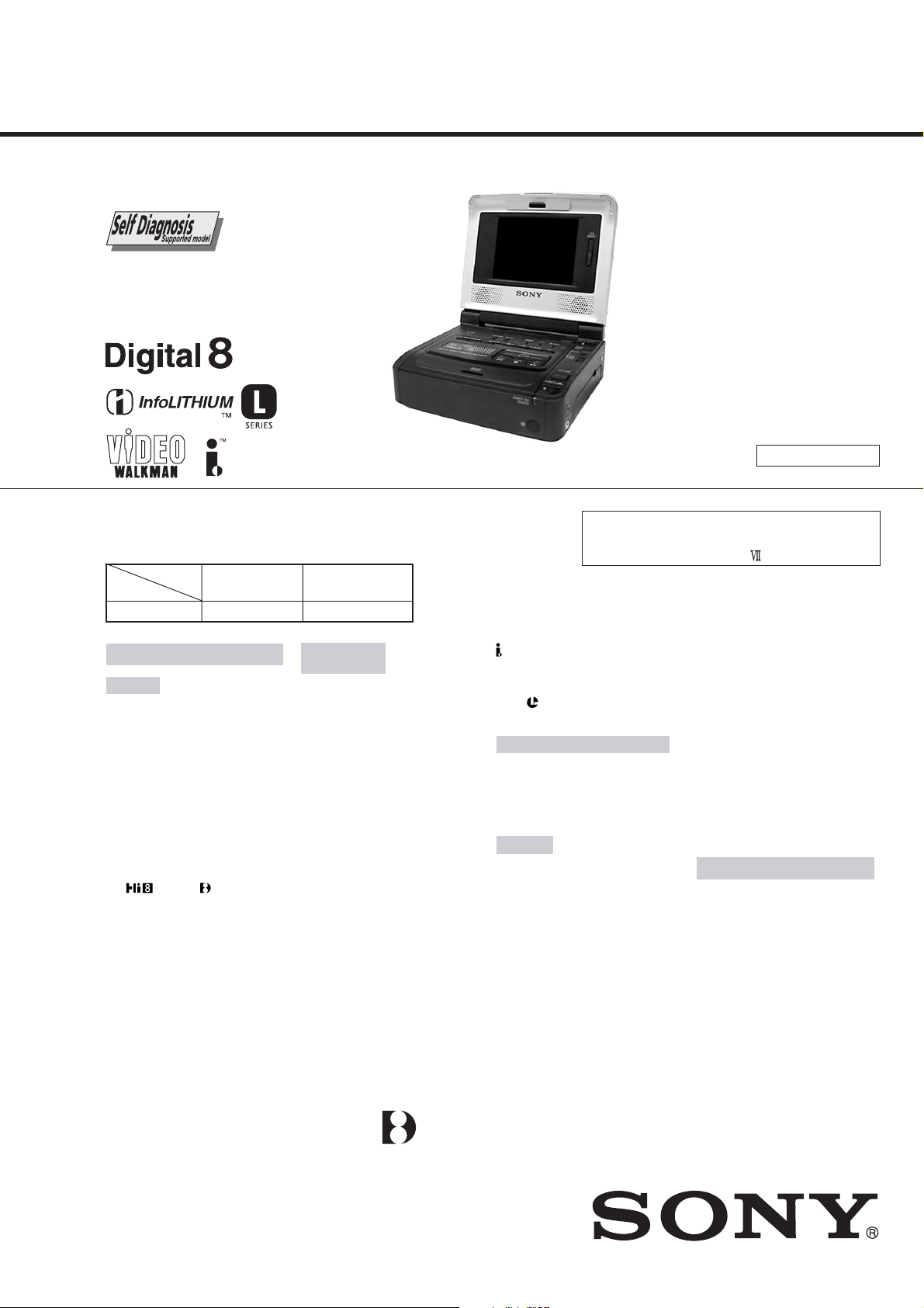
Photo : GV-D800E
NTSC MODEL : GV-D200/D800
PAL MODEL : GV-D200E/D800E
Function difference table
Model
Function
LCD
GV-D200/200E
—
VCR
System
Video recording system
2 rotary heads
Helical scanning system
Audio recording system
Rotary heads, PCM system
Quantization: 12 bits (Fs 32 kHz,
stereo 1, stereo 2), 16 bits (Fs 48 kHz,
stereo)
Video signal
GV-D200/D800:
NTSC color, EIA standards
GV-D200E/D800E:
PAL colour, CCIR standards
Recommended cassette
Hi8
Recording/playback time
(GV-D200/D800: using
120 min. Hi8 video cassette)
(GV-D200E/D800E: using
90 min. Hi8 (PAL) video cassette)
SP mode: 1 hour
LP mode: 1 hour and 30 minutes
Fastforward/rewind time
(GV-D200/D800: using
120 min. Hi8 video cassette)
(GV-D200E/D800E: using
90 min. Hi8 (PAL) video cassette)
Approx. 5 minutes and 15 seconds
/Digital8 video cassette
GV-D800/D800E
4.0 inches
SPECIFICATIONS
Input/output
connectors
S video input
4-pin mini DIN
Luminance signal: 1 Vp-p, 75 ohms,
unbalanced
GV-D200/D800:
Chrominance signal: 0.286 Vp-p
GV-D200E/D800E:
Chrominance signal: 0.3 Vp-p,
75 ohms, unbalanced
S video output
4-pin mini DIN
Luminance signal: 1 Vp-p, 75 ohms,
unbalanced
GV-D200/D800:
Chrominance signal: 0.286 Vp-p
GV-D200E/D800E:
Chrominance signal: 0.3 Vp-p,
75 ohms, unbalanced
Audio/Video input
AV MINIJACK
Video: 1 Vp-p, 75 ohms, unbalanced,
sync negative
Audio: 327 mV, input impedance
more than 47 kiloohms
Video output
Phono jack, 1 Vp-p, 75 ohms,
unbalanced, sync negative
Audio output
Phono jacks (2) 327 mV, output
impedance less than 1 kiloohm
RFU DC OUT
Special minijack DC 5 V
DV input/output
4-pin connector
Headphone jack
Stereo minijack (ø 3.5 mm)
LANC
Stereo mini-minijack (ø 2.5 mm)
LCD screen (GV-D800/D800E)
Picture
4.0 type
80.6 × 60.5 mm (3 1/4 × 2 1/2 in.)
Total dot number
123,200 (560 × 220)
General
Power requirements
7.2 V (battery pack)
8.4 V (AC power adaptor)
Average power consumption
(when using the battery pack)
GV-D800/D800E only
During playback using LCD
4.9 W
During playing back when you close
the LCD panel
3.0 W
Operating temperature
0 °C to 40 °C (32 °F to 104 °F)
Storage temperature
–20 °C to +60 °C (–4 °F to +140 °F)
jack
US Model
Canadian Model
GV-D200/D800
AEP Model
UK Model
E Model
GV-D200E/D800E
B MECHANISM
For MECHANISM ADJUSTMENT, refer to
the “8mm Video MECHANICAL
ADJUSTMENT MANUAL
Dimensions (Approx.)
GV-D200/D200E:
148 × 50 × 135 mm
(5 7/8 × 2 × 5 3/8 in.)
GV-D800/D800E:
148 × 65 × 135 mm
(5 7/8 × 2 5/8 × 5 3/8 in.) (w/h/d)
Mass (approx.)
GV-D200/D200E:
660 g (1 lb 7 oz)
GV-D800/D800E:
930 g (2 lb)
excluding the battery pack and
cassette
Supplied accessories
See page 2.
AC power adaptor
Power requirements
100 - 240 V AC, 50/60 Hz
Power consumption
23 W
Output voltage
DC OUT: 8.4 V, 1.5 A in the
operating mode
Operating temperature
0 °C to 40 °C (32 °F to 104 °F)
Storage temperature
–20 °C to +60 °C (–4 °F to +140 °F)
” (9-973-801-11).
— Continued on next page —
DIGITAL VIDEO CASSETTE RECORDER
Dimensions (approx.)
125 × 39 × 62 mm
(5 × 1 9/16 × 2 1/2 in.) (w/h/d)
excluding projecting parts
Mass (approx.)
280 g (9.8 oz) excluding power cord
Cord length (approx.)
Power cord: 2 m (6.6 feet)
Connecting cord: 1.6 m (5.2 feet)
Design and specifications are subject
to change without notice.
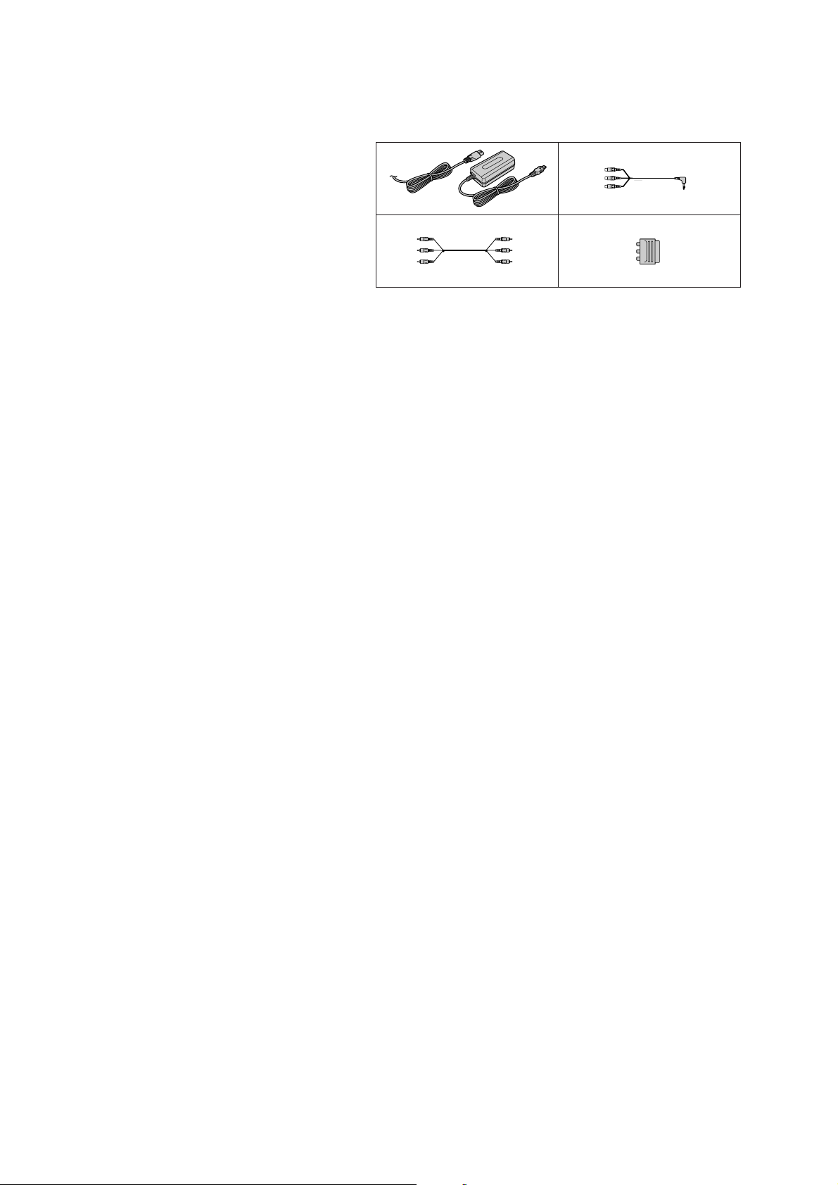
• SUPPLIED ACCESSORIES
Make sure that the following accessories are supplied with your VCR.
21
43
SAFETY-RELATED COMPONENT WARNING!!
COMPONENTS IDENTIFIED BY MARK 0 OR DOTTED LINE WITH
MARK 0 ON THE SCHEMATIC DIAGRAMS AND IN THE PARTS
LIST ARE CRITICAL TO SAFE OPERATION. REPLACE THESE
COMPONENTS WITH SONY PARTS WHOSE PART NUMBERS
APPEAR AS SHOWN IN THIS MANUAL OR IN SUPPLEMENTS
PUBLISHED BY SONY.
1 AC-L10A/L10B/L10C AC power adaptor (1),
Mains lead (1)
23A/V converting cable (1)
ATTENTION AU COMPOSANT AYANT RAPPORT
LES COMPOSANTS IDENTIFÉS P AR UNE MARQUE 0 SUR LES
DIAGRAMMES SCHÉMA TIQUES ET LA LISTE DES PIÈCES SONT
CRITIQUES POUR LA SÉCURITÉ DE FONCTIONNEMENT. NE
REMPLACER CES COMPOSANTS QUE PAR DES PIÈSES SONY
DONT LES NUMÉROS SONT DONNÉS DANS CE MANUEL OU
DANS LES SUPPÉMENTS PUBLIÉS PAR SONY.
À LA SÉCURITÉ!
A/V connecting cable (1)
4 21-pin adaptor (1)
GV-D200E/D800E only
SAFETY CHECK-OUT
After correcting the original service problem, perform the following
safety checks before releasing the set to the customer.
1. Check the area of your repair for unsoldered or poorly-soldered
connections. Check the entire board surface for solder splashes
and bridges.
2. Check the interboard wiring to ensure that no wires are
"pinched" or contact high-wattage resistors.
3. Look for unauthorized replacement parts, particularly
transistors, that were installed during a previous repair . Point
them out to the customer and recommend their replacement.
4. Look for parts which, through functioning, show obvious signs
of deterioration. Point them out to the customer and
recommend their replacement.
5. Check the B+ voltage to see it is at the values specified.
6. Flexible Circuit Board Repairing
• Keep the temperature of the soldering iron around 270˚C
during repairing.
• Do not touch the soldering iron on the same conductor of the
circuit board (within 3 times).
• Be careful not to apply force on the conductor when soldering
or unsoldering.
— 2 —

TABLE OF CONTENTS
SERVICE NOTE
1. POWER SUPPLY DURING REPAIRS ····························· 6
2. TO TAKE OUT A CASSETTE WHEN NOT EJECT
(FORCE EJECT) (1) ·························································· 6
3. TO TAKE OUT A CASSETTE WHEN NOT EJECT
(FORCE EJECT) (2)
(TO TAKE OUT A CASSETTE WITHOUT
HURTING THE TAPE) ······················································ 7
SELF-DIAGNOSIS FUNCTION
1. SELF-DIAGNOSIS FUNCTION······································· 8
2. SELF-DIAGNOSIS DISPLAY ·········································· 8
3. SERVICE MODE DISPLAY ············································· 8
3-1. Display Method ·································································· 8
3-2. Switching of Backup No. ··················································· 8
3-3. End of Display····································································8
4. SELF-DIAGNOSIS CODE TABLE ···································9
2-4. PD-130, LS-56 BOARDS (D800, D800E MODEL) ······2-4
2-5. LCD WINDOW CABINET ASSEMBLY (SP-901, 902)
(D800, D800E MODEL) ·················································2-5
2-6. BATTERY PANEL ASSEMBLY, BATTERY TERMINAL
BOARD, DC-IN CONNECTOR·····································2-6
2-7. VC-250, FU-145 BOARDS·············································2-6
2-8.
CONTROL SWITCH BLOCK (FK-78), LOADING LID ··
2-9. MECHANISM DECK, MAIN FRAME ASSEMBLY ···2-7
2-10. CABINET (R) BLOCK ASSEMBLY, JACK FRAME
(IO-68, IR-38 BOARDS) ················································2-8
2-11. EX-36 BOARD, FP-570 FLEXIBLE BOARD···············2-9
2-12. UPPER CABINET ASSEMBLY,
LCD BLOCK ASSEMBLY (D800, D800E MODEL)····2-9
2-13. HINGE UNIT, FP-569 FLEXIBLE BOARD
(D800, D800E MODEL) ···············································2-10
2-14. CIRCUIT BOARDS LOCATION ·································2-12
2-15. FLEXIBLE BOARDS LOCATION ······························2-13
2-7
1. GENERAL
Getting started
Using this manual ··································································1-1
Checking supplied accessories ··············································1-1
Step 1 Preparing the power supply ········································1-1
Connecting to the mains ····················································· 1-1
Using with a battery pack (not supplied) ···························· 1-2
Step 2 Inserting a cassette····················································· 1-2
Basic operations
Playing back a tape ······························································· 1-3
Viewing the recording on TV ················································1-4
Recording from the other VCR or TV ···································1-5
Advanced operations
Enlarging playback images – PB ZOOM ······························1-6
Watching a tape with special effects – Picture effect·············1-7
Watching a tape with special performances – Digital effect··1-7
Quickly locating a scene – Zero set memory·························1-8
Searching with recording date – Date search ························1-8
Searching for a photo – Photo search/Photo scan··················1-9
Displaying recording data and screen indicators
– Data code function ······························································1-9
Superimposing a title ···························································1-10
Making your own titles ························································1-10
Editing
Dubbing a tape ·····································································1-11
Dubbing only desired scenes – Digital program editing ·····1-12
Using with an analogue video unit and a personal computer
– Signal convert function·····················································1-15
Inserting a scene from the other (playback) VCR
– Insert Editing ····································································1-15
Customizing your VCR
Changing the menu settings·················································1-16
Resetting the date and time··················································1-17
Additional information
Digital8
About i.LINK·······································································1-19
Troubleshooting ···································································1-19
Self-diagnosis display ··························································1-20
Warning indicators and messages ········································1-20
Using your VCR abroad ······················································ 1-21
Maintenance information and precautions···························1-21
Quick reference
Identifying the parts and controls ········································ 1-22
system, recording, and playback·······················1-18
2. DISASSEMBLY
2-1. CASSETTE LID ASSEMBLY ········································2-2
2-2. BOTTOM CABINET ASSEMBLY, FP-571 FLEXIBLE
BOARD (LITHIUM BATTERY) ····································2-2
2-3.
LCD CABINET ASSEMBLY (D800, D800E MODEL)··
2-3
3. BLOCK DIAGRAMS
3-1. OVERALL BLOCK DIAGRAM (1/4) ···························3-1
3-2. OVERALL BLOCK DIAGRAM (2/4) ···························3-3
3-3. OVERALL BLOCK DIAGRAM (3/4) ···························3-5
3-4. OVERALL BLOCK DIAGRAM (4/4) ···························3-7
3-5. POWER BLOCK DIAGRAM (1/2)································3-9
3-6. POWER BLOCK DIAGRAM (2/2)······························3-11
4. PRINTED WIRING BOARDS AND
SCHEMATIC DIAGRAMS
4-1. FRAME SCHEMATIC DIAGRAM (1/2)·······················4-1
FRAME SCHEMATIC DIAGRAM (2/2)·······················4-3
4-2. PRINTED WIRING BOARDS AND
SCHEMATIC DIAGRAMS ············································4-5
• VC-250 (REC/PB AMP, DAC, DV INTERFACE,
AD CONVERTER, Y/C PROCESSOR, LINE A/D,
LINE I/O, IR, AUDIO I/O, DRUM/CAPSTAN
MOTOR DRIVE, MECHA CONTROL, HI CONTROL,
DC/DC CONVERTER, CONNECTION)
PRINTED WIRING BOARD ·························4-7
• VC-250 (REC/PB AMP)(1/16)
SCHEMATIC DIAGRAM····························4-11
• VC-250 (PB AMP, DAC)(2/16)
SCHEMATIC DIAGRAM····························4-13
• VC-250 (DV INTERFACE)(3/16)
SCHEMATIC DIAGRAM····························4-15
• VC-250 (DV INTERFACE)(4/16)
SCHEMATIC DIAGRAM····························4-17
• VC-250 (AD CONVERTER)(5/16)
SCHEMATIC DIAGRAM····························4-19
• VC-250 (Y/C PROCESSOR)(6/16)
SCHEMATIC DIAGRAM····························4-21
• VC-250 (LINE A/D)(7/16)
SCHEMATIC DIAGRAM····························4-23
• VC-250 (LINE IN/OUT)(8/16)
SCHEMATIC DIAGRAM····························4-25
• VC-250 (IR)(9/16)
SCHEMATIC DIAGRAM····························4-27
• VC-250 (MECHANISM CONTROL)(10/16)
SCHEMATIC DIAGRAM····························4-29
• VC-250 (AUDIO I/O)(11/16)
SCHEMATIC DIAGRAM····························4-31
• VC-250 (DRUM/CAPSTAN MOTOR DRIVE)(12/16)
SCHEMATIC DIAGRAM····························4-33
• VC-250 (MECHA CONTROL)(13/16)
SCHEMATIC DIAGRAM····························4-35
• VC-250 (HI CONTROL)(14/16)
SCHEMATIC DIAGRAM····························4-37
— 3 —

• VC-250 (DC/DC CONVERTER)(15/16)
SCHEMATIC DIAGRAM····························4-39
• VC-250 (CONNECTION)(16/16)
SCHEMATIC DIAGRAM····························4-41
• FP-575 (LANC), IO-68 (AV IN/OUT)
PRINTED WIRING BOARDS ·····················4-43
• IO-68 (AV IN/OUT)
SCHEMATIC DIAGRAM····························4-45
• FU-145 (DC/DC CONVERTER)
PRINTED WIRING BOARD ·······················4-47
• FU-145 (DC/DC CONVERTER)
SCHEMATIC DIAGRAM····························4-49
• PD-130 (LCD DRIVER, BACK-LIGHT)
PRINTED WIRING BOARD ·······················4-51
• LS-56 (LCD SWITCH)
PRINTED WIRING BOARD ·······················4-54
• PD-130 (LCD DRIVER, BACK-LIGHT)(1/2)
SCHEMATIC DIAGRAM····························4-55
• PD-130 (BACK-LIGHT)(2/2)
SCHEMATIC DIAGRAM····························4-57
• IR-38 (IR TRANSMITTER),
CONTROL SWITCH BLOCK (FK-78)
PRINTED WIRING BOARDS ·····················4-59
• CONTROL SWITCH BLOCK (FK-78)
SCHEMATIC DIAGRAM····························4-61
• EX-36 (MULTI CONNECTOR)
PRINTED WIRING BOARD ·······················4-63
• EX-36 (MULTI CONNECTOR)
SCHEMATIC DIAGRAM····························4-65
• FP-571 (BATTERY), FP-249 (S/T REEL)
PRINTED WIRING BOARDS ·····················4-67
4-3. WAVEFORMS ······························································4-68
4-4. MOUNTED PARTS LOCATION ·································4-70
5. ADJUSTMENTS
1. Before starting adjustment···············································5-1
1-1. Adjusting items when replacing main parts and boards.·5-2
5-1. ADJUSTMENT PREPARATIONS·································5-3
1-1. PREPARATIONS BEFORE ADJUSTMENT·················5-3
1-1-1.List of Service Tools ························································5-3
5-2. MECHANISM SECTION ADJUSTMENT····················5-4
2-1. Hi8/STANDARD8 MODE··············································5-4
2-1-1.OPERA TING WITHOUT CASSETTE ··························5-4
2-1-2.TAPE PATH ADJUSTMENT··········································5-4
1. Preparations for Adjustment············································ 5-4
2-2. DIGITAL8 MODE ··························································5-5
2-2-1.HOW TO ENTER RECORD MODE WITHOUT
CASSETTE ····································································· 5-5
2-2-2.HOW TO ENTER PLAYBACK MODE WITHOUT
CASSETTE ····································································· 5-5
2-2-3.OVERALL TAPE PATH CHECK ···································5-5
1. Recording of the tape path check signal·························· 5-5
2. Tape path check ······························································· 5-5
5-3. ELECTRICAL ADJUSTMENT······································5-6
3-1. PREPARATIONS BEFORE ADJUSTMENTS ·············· 5-6
3-1-1.Equipment to Required····················································5-6
3-1-2.Precautions on Adjusting·················································5-7
3-1-3.Adjusting Connectors ······················································5-7
3-1-4.Connecting the Equipment ·············································· 5-8
3-1-5.Alignment Tape ·······························································5-9
3-1-6.Input/output Level and Impedance ································5-10
3-2. INITIALIZATION OF C, D, E, F, 7, 8 PAGE DATA ···5-11
3-2-1.INITIALIZATION OF C, D, 8 PAGE DATA ················5-11
1. Initializing the C, D, 8 Page Data··································5-11
2. Modification of C, D, 8 Page Data ································5-11
3. C Page Table ··································································5-11
4. D Page Table··································································5-12
5. 8 Page Table···································································5-13
3-2-2.INITIALIZATION OF E, F, 7 PAGE DATA ·················5-14
1. Initializing the E, F, 7 Page Data ···································5-14
2. Modification of E, F, 7 Page Data ·································5-14
3. F Page Table ··································································5-14
4. E Page Table ··································································5-15
5. 7 Page Table···································································5-16
3-3. SYSTEM CONTROL SYSTEM ADJUSTMENT········5-17
1. Serial No. Input ·····························································5-17
1-1. Company ID Input·························································5-17
1-2. Serial No. Input ·····························································5-17
2. Battery End Adjustment ················································5-19
3-4. SERVO AND RF SYSTEM ADJUSTMENT ···············5-20
1. REEL FG Adjustment (VC-250 Board) ························5-20
2. PLL fo & LPF fo Pre-Adjustment (VC-250 Board)······5-20
3. Switching Position Adjustment (VC-250 Board)··········5-21
4. AGC Center Level and APC & AEQ Adjustment ·········5-21
4-1. Preparations before adjustments····································5-21
4-2. AGC Center Level Adjustment (VC-250 Board) ··········5-21
4-3. APC & AEQ Adjustment (VC-250 Board) ···················5-22
4-4. Processing after Completing Adjustments ···················· 5-22
5. PLL fo & LPF fo Final Adjustment (VC-250 Board) ···5-23
6. Hi8/Standard8 Switching Position Adjustment
(VC-250 Board)·····························································5-23
7. CAP FG Offset Adjustment (VC-250 board) ················5-24
3-5. VIDEO SYSTEM ADJUSTMENTS·····························5-25
1.
27MHz Origin Oscillation Adjustment (VC-250 board) ··
2. Chroma BPF fo Adjustment (VC-250 Board)···············5-25
3. S VIDEO OUT Y Level Adjustment (VC-250 Board) ··5-26
4. S VIDEO OUT Chroma Level Adjustment
(VC-250 Board)·····························································5-26
5.
VIDEO OUT Y, Chroma Level Check (VC-250 Board) ··
Hi8/Standard8 Y/C Output Level Setting (VC-250 Board)·
6.
7.
Hi8/standard 8mm AFC fo Adjustment (VC-250 board) ··
3-6. IR TRANSMITTER ADJUSTMENTS·························5-29
1.
IR Video Carrier Frequency Adjustment (VC-250 board)··
2. IR Video Deviation Adjustment (VC-250 board) ··········5-29
3. IR Audio Deviation Adjustment (VC-250 board) ·········5-30
3-7. AUDIO SYSTEM ADJUSTMENTS ····························5-31
1.
Hi8/Standard8 AFM BPF fo Adjustment (VC-250 board)··
2. Hi8/Standard8 AFM 1.5 MHz Deviation Adjustment
(VC-250 board) ·····························································5-32
3. Hi8/Standard8 AFM 1.7 MHz Deviation Adjustment
(VC-250 board) ·····························································5-32
4. Digital8 Playback Level Check ·····································5-32
5. Overall Level Characteristics Check ·····························5-32
6. Overall Distortion Check···············································5-32
7. Overall Noise Level Check············································5-33
8. Overall Separation Check·············································· 5-33
3-8. LCD SYSTEM ADJUSTMENT (GV-D800/D800E) ···5-34
1. LCD Initial Data Input (1)·············································5-34
2. LCD Initial Data Input (2)·············································5-35
3. VCO Adjustment (PD-130 board)·································5-35
4. RGB AMP Adjustment (PD-130 board)························5-36
5. Contrast Adjustment (PD-130 board)····························5-36
6. COM AMP Adjustment (PD-130 board)·······················5-37
7. V-COM Adjustment (PD-130 board) ····························5-37
8. White Balance Adjustment (PD-130 board)··················5-38
5-4. SERVICE MODE··························································5-39
4-1. ADJUSTMENT REMOTE COMMANDER ················5-39
1. Using the Adjustment Remote Commander··················5-39
2. Precautions Upon Using the Adjustment Remote
Commander ··································································· 5-39
4-2. DATA PROCESS···························································5-40
4-3. SERVICE MODE··························································5-41
1. Setting the Test Mode ····················································5-41
2. Emergence Memory Address ········································5-41
5-25
5-27
5-27
5-28
5-29
5-31
— 4 —

2-1. C Page Emergence Memory Address ····························5-41
2-2. F Page Emergence Memory Address ····························5-42
2-3. EMG Code (Emergency Code) ·····································5-42
2-4. MSW Code ····································································5-43
3. Bit V alue Discrimination ···············································5-44
4. Switch check (1) ····························································5-44
5. Switch check (2) ····························································5-44
6. Switch check (3) ····························································5-44
7. Switch check (4) ····························································5-45
8. Record of Use check······················································5-45
9. Record of Self-diagnosis check ·····································5-46
6. REPAIR PARTS LIST
6-1. EXPLODED VIEWS ······················································6-1
6-1-1.OVERALL SECTION-1 ················································· 6-1
6-1-2.OVERALL SECTION-2 ················································· 6-2
6-1-3.LCD SECTION (D800/D800E MODEL) ·······················6-3
6-1-4.MECHANISM SECTION···············································6-4
6-1-5.CASSETTE COMPARTMENT ASSEMBLY ················6-5
6-1-6.LS CHASSIS ASSEMBLY ·············································6-6
6-1-7.MECHANISM CHASSIS ASSEMBLY ························· 6-7
6-2. ELECTRICAL PARTS LIST ··········································6-8
— 5 —
SERVICE NOTE
1. POWER SUPPLY DURING REPAIRS
In this unit, about 10 seconds after power is supplied (8.4V) to the battery terminal using the service power code (J-6082-223-A), the power
is shut off so that the unit cannot operate.
These following two methods are available to prevent this. Take note of which to use during repairs.
Method 1:
Connect the adjustment remote commander RM-95 (J-6082-053-B) to the LANC jack, and set the HOLD switch to the “ADJ” side.
Method 2:
Use the DC IN terminal. (Use the AC power adaptor. (AC-L10, AC-VQ800 etc.))
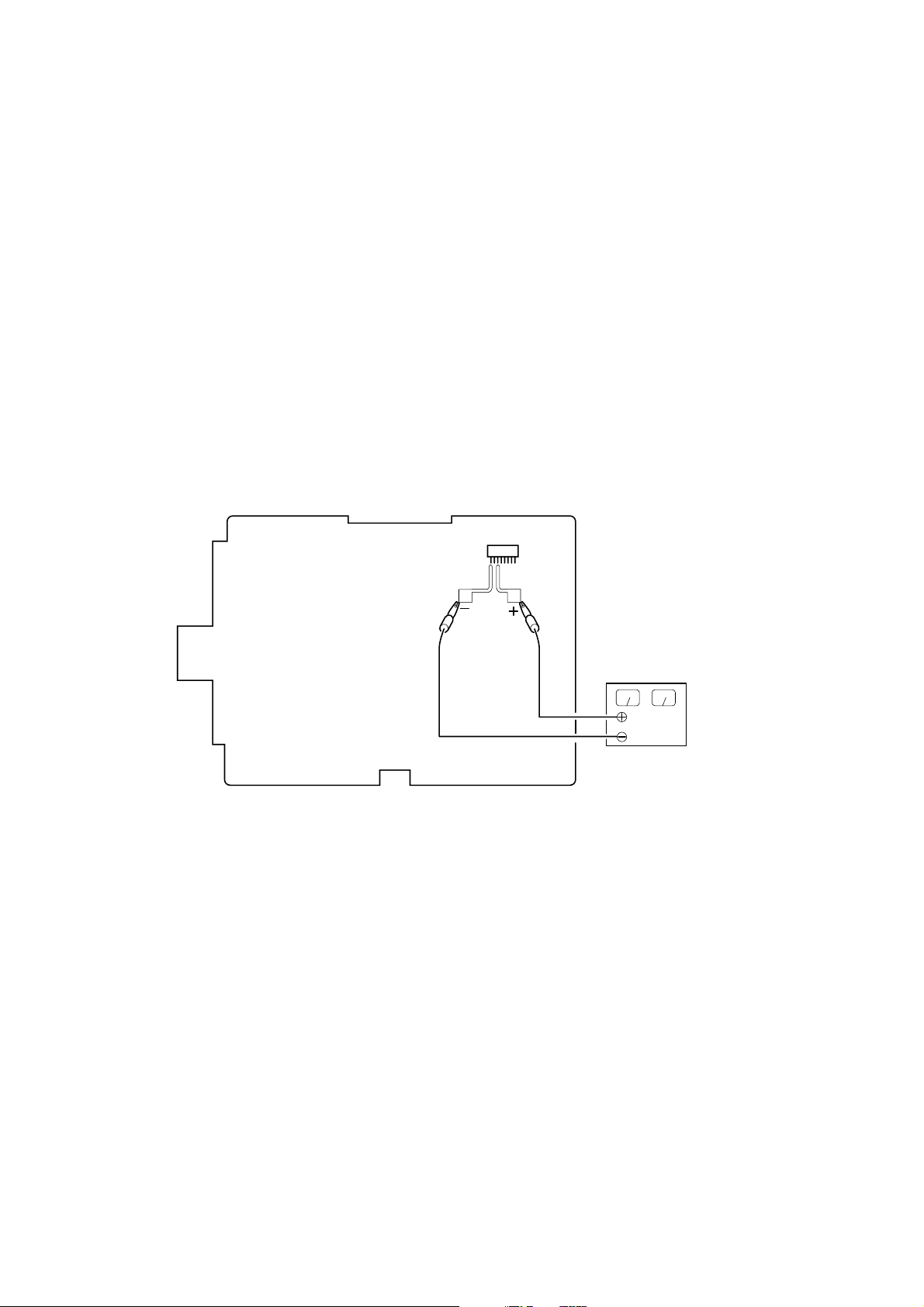
2. TO TAKE OUT A CASSETTE WHEN NOT EJECT (FORCE EJECT) (1)
1 Remove the power supply (Battery or AC power adaptor).
2 Push the EJECT switch and open the cassette lid.
3 Refer to 2-2. to remove the cabinet (lid) assembly.
4 Refer to 2-2. to remove the cabinet (bottom) assembly.
5 Add 5V from the regulated power supply between Pin 5, 6 of CN4401 (ULD5V +) and Pin 7, 8 of CN4401 (ULD5V –), and unload
the cassette.
VC-250 board
CN4401
8
ULD
5V
1
Regulated
power supply (+5V)
— 6 —
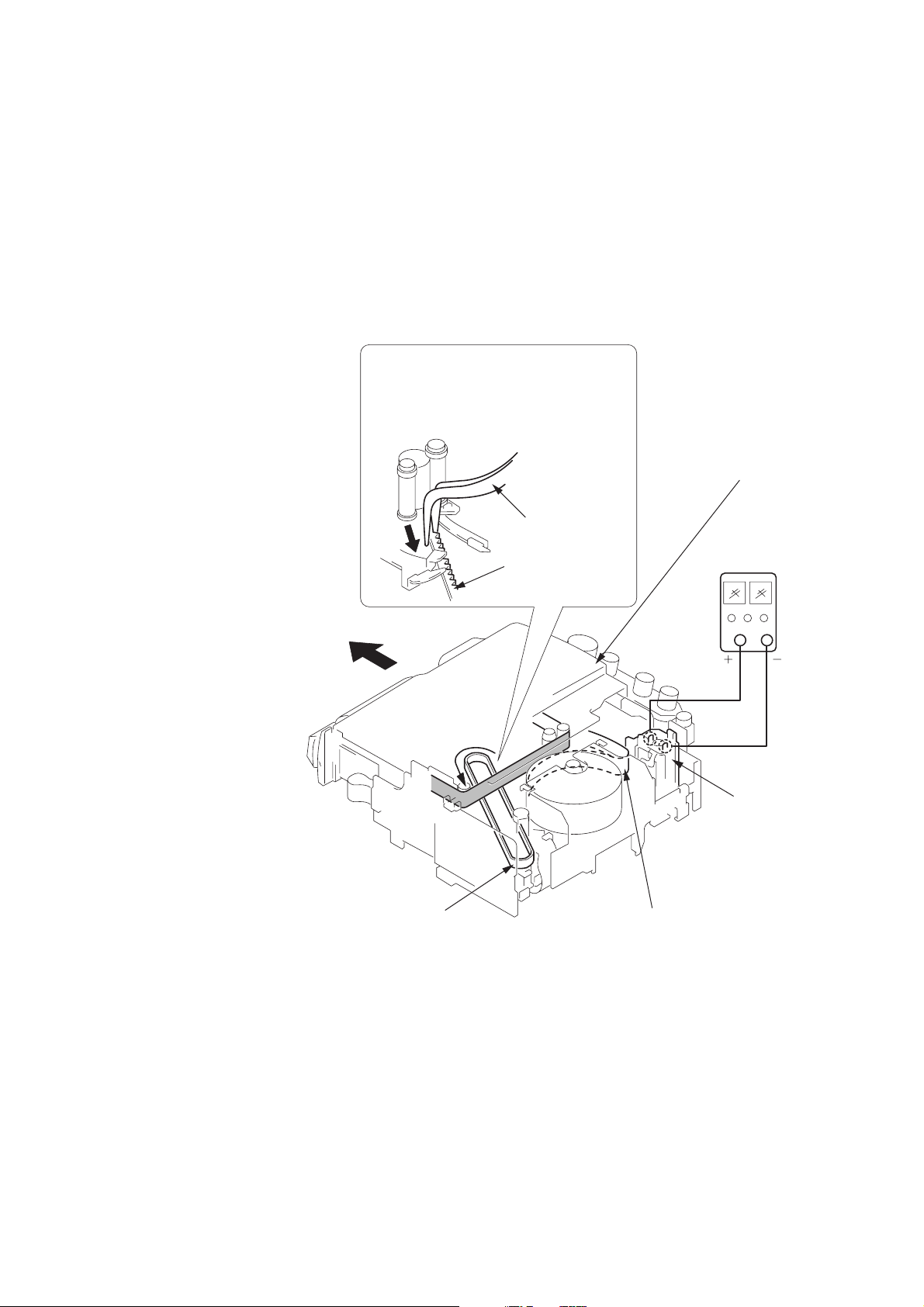
3. TO TAKE OUT A CASSETTE WHEN NOT EJECT (FORCE EJECT) (2)
(TO TAKE OUT A CASSETTE WITHOUT HURTING THE TAPE)
1 Disconnect the power supply (Battery or AC adaptor)
2 Refer to 2-2. to remove the cabinet (lid) assembly.
3 Refer to 2-2. to remove the cabinet (bottom) assembly.
4 Refer to 2-1. to remove the Cassette (lid) assembly.
5 Refer to 2-6 to 2-8. to remove the LCD block (GV-D800/D800E only) and the cabinet (upper) assembly.
6 Remove the FU-145 board.
7 Refer to 2-9. to remove the lid frame assembly.
8 Add +5V from the regulated power supply and unload with a pressing the cassette lid.
9
Pull the timing belt in the direction of
A
arrow
the cassette lid (take care not to damage)
to adjust the bending of a tape.
with a pincette while pressing
Press the cassette lid not to rise
the cassette compartment
0
Let go your hold the cassette
lid and rise the cassette
compartment to take out a cassette.
Timing belt
Pincette
Timing belt
Regulated
power supply
(+5V)
Loading motor
Adjust the bending of a tape
— 7 —
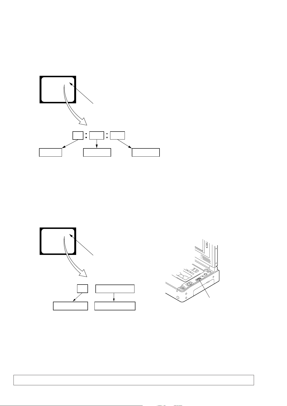
SELF-DIAGNOSIS FUNCTION
1. SELF-DIAGNOSIS FUNCTION
When problems occur while the unit is operating, the self-diagnosis
function starts working, and displays on the LCD screen or monitor
TV (Note) what to do. This function consists of two display; selfdiagnosis display and service mode display.
Details of the self-diagnosis functions are provided in the Instruction
manual.
LCD screen or monitor TV
C : 3 1 : 1 1
Repaired by:
C : Corrected by customer
H : Corrected by dealer
E : Corrected by service
engineer
Blinks at 3.2Hz
3 1C
Block
Indicates the appropriate
step to be taken.
E.g.
31 ....Reload the tape.
32 ....Turn o n power again.
1 1
2. SELF-DIAGNOSIS DISPLAY
When problems occur while the unit is operating, the counter of the
viewfinder shows a 4-digit display consisting of an alphabet and
numbers, which blinks at 3.2 Hz. This 5-character display indicates
the “repaired by:”, “block” in which the problem occurred, and
“detailed code” of the problem.
Note: Set the DISPLAY in the menu system to V-OUT/LCD only for the
model with LCD screen, and press the DISPLAY button.
Detailed Code
Refer to page 9.
Self-diagnosis Code Table.
3. SER VICE MODE DISPLAY
The service mode display shows up to six self-diagnosis codes shown in the past.
3-1. Display Method
While pressing the “STOP” key , set the PO WER switch from OFF to ON, and continue pressing the “STOP” ke y for 10 seconds continuously .
The service mode will be displayed, and the counter will show the backup No. and the 5-character self-diagnosis codes.
LCD screen or monitor TV
[3] C : 3 1 : 1 1
Lights up
[3]
Backup No.
Order of previous errors
3-2. Switching of Backup No.
By rotating the control dial, past self-diagnosis codes will be shown in order. The backup No. in the [] indicates the order in which the
problem occurred. (If the number of problems which occurred is less than 6, only the number of problems which occurred will be shown.)
[1] : Occurred first time [4] : Occurred fourth time
[2] : Occurred second time [5] : Occurred fifth time
[3] : Occurred third time [6] : Occurred the last time
C : 3 1 : 1 1
Control dial
self-diagnosis codes
3-3. End of Display
Turning OFF the power supply will end the service mode display.
Note: The “self-diagnosis displa y” data will be backed up by the coin-type lithium battery of FP-571 flexible board. When this coin-type lithium ba ttery
is removed, the “self-diagnosis display” data will be lost by initialization.
— 8 —
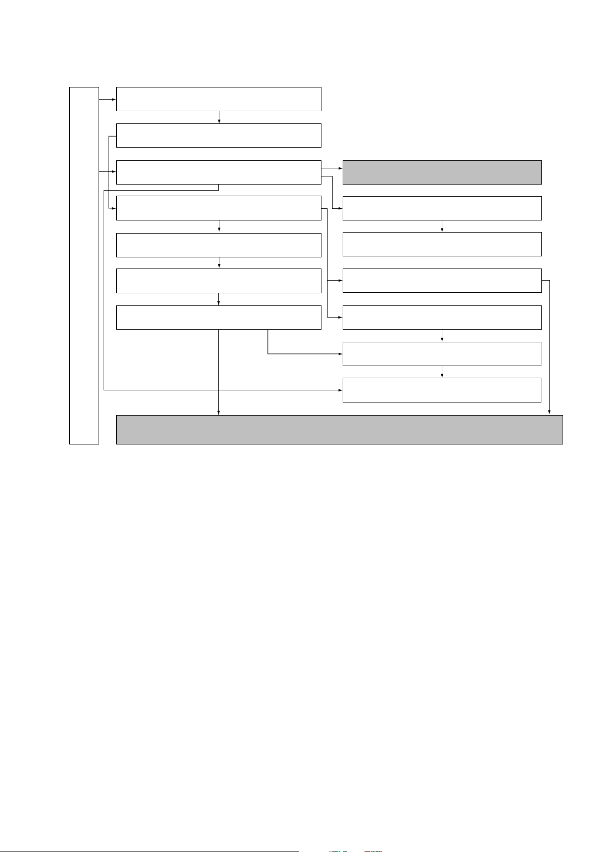
SECTION 2
DISASSEMBLY
The following flow chart shows the disassembly procedure.
2-1. Cassette Lid assembly
2-2. Bottom cabinet assembly, FP-571 flexible board
(Lithium battery)
GV-D200/D200E/D800/D800E
2-3. LCD cabinet assembly (D800, D800E model)
2-6. Battery panel assembly, Battery terminal board,
DC-IN connector
2-7. VC-250, FU-145 boards
2-9. Mechanism deck, Main frame assembly
2-10. Cabinet (R) block assembly, Jack frame
(IO-68, IR-38 boards)
GV-D200/D200E/D800/D800E
[CONNECTION DIAGRAM FOR SERVICE POSITION (Mainly for voltage measurement and check)]
(VC-250, FU-145, IO-68 boards, Mechanism deck)
PD-130 board service position
(D800, D800E model)
2-4. PD-130, LS-56 boards (D800, D800E model)
2-5. LCD window cabinet assembly (SP-901,902)
(D800, D800E model)
2-8. Control switch block (FK-78), Loading lid
2-11. EX-36 board, FP-570 flexible board
2-12. Upper cabinet assembly,
LCD block assembly (D800, D800E model)
2-13. Hinge unit , FP-569 flexible board
(D800, D800E model)
2-1
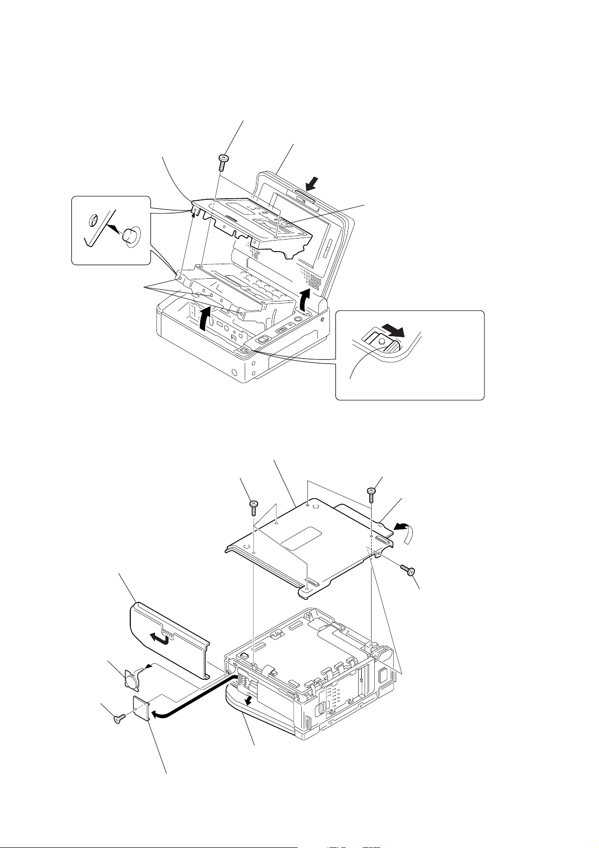
NOTE: F ollo w the disassembly procedure in the numerical order given.
2-1. CASSETTE LID ASSEMBLY
2
Two screws (M2 × 4),
lock ace, p2
1
Open the LCD panel in the
direction of the arrow A.
(GV-D800/D800E model)
A
4
Three dowels
6
Cassette lid
assembly
Push
5
Claw
Press the cassette EJECT knob to
3
open the cassette compartment.
2-2. BOTTOM CABINET ASSEMBLY, FP-571 FLEXIBLE BOARD (LITHIUM BATTERY)
7
Bottom cabinet assembly
3
2
Press the release button to remove
the cabinet lid assembly in the
direction of the arrow
A
0
FP-571 flexible board
(4P)
Three screws (M2 × 4),
lock ace, p2
A
.
Board
VC-250
4
Two screws (M2 × 4),
lock ace, p2
6
Open the jack lid assembly
in the direction of the arrow
B
5
Screw (M2 × 4),
lock ace, p2
B
.
8
T apping screw
×
(+k 2
5)
C
9
Remove the lithium lid in the
direction of the arrow
1
Open the LCD panel little.
(GV-D800/D800E model)
C
.
2-2
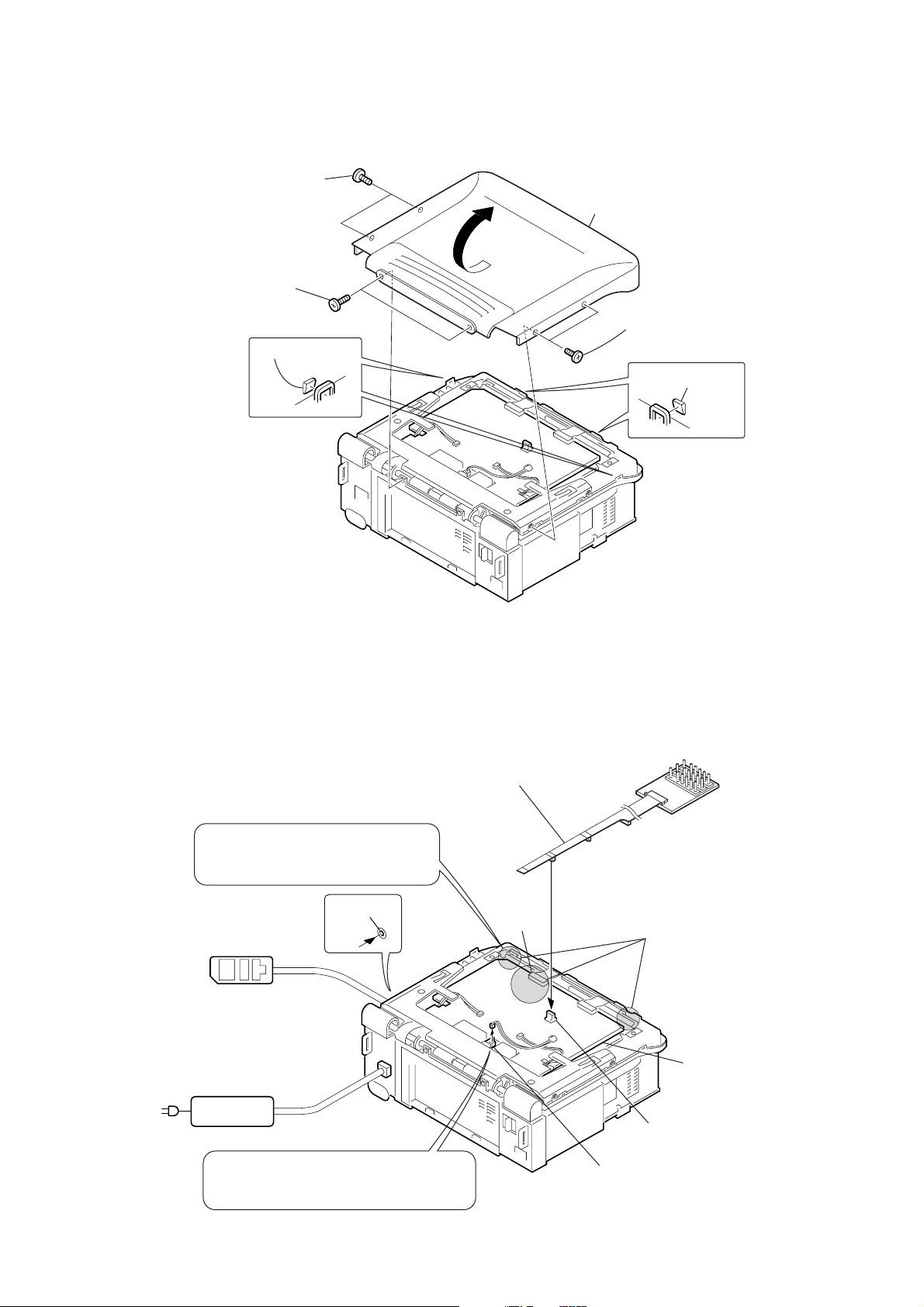
2-3. LCD CABINET ASSEMBLY (D800, D800E MODEL)
2
Two screws (M2 × 4),
lock ace, p2
3
Two screws (M2 × 3),
lock ace, p2
4
Two
claws
6
Remove the LCD cabinet assembly
in the direction of the arrow.
1
Two screws (M2 × 4),
lock ace, p2
5
Two
claws
[PD-130 BOARD SERVICE POSITION]
(D800, D800E MODEL)
Touching here is safe when the machine
is normal. However touching here can be
dangerous if defective parts exist.
LANC
jack
Adjustment remote
commander (RM-95)
AC IN
AC POWER
ADAPTOR
Multi-CPC jig
(J-6082-311-A)
CN5607
PD-130
Board
Caution
High voltage
1
2
9
10
PD-130 board
CN5502
When the hinge unit is closed to be laid down,
remove CN01 (2P) on the LS-56 board.
If not, the main power cannot be turned on.
LS-56 board
CN01 (2P)
2-3
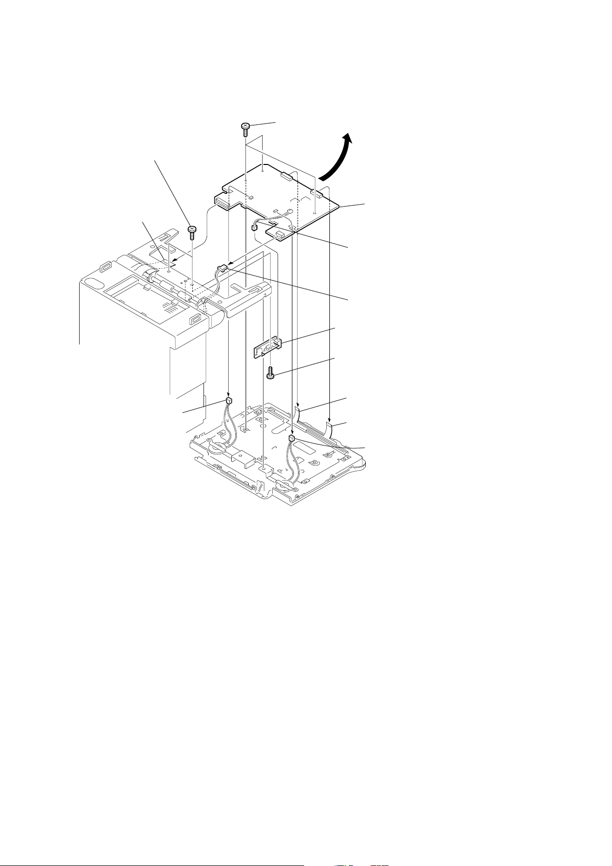
2-4. PD-130, LS-56 BOARDS (D800, D800E MODEL)
9
Three screws (M2 × 3),
lock ace, p2
6
Two tapping screws
(B2
×
5)
PD-130
Board
7
FP-569 flexible
board (26, 32P)
0
Remove the PD-130 board
in the direction of the arrow.
3
Harness (PL-53) (2P)
8
Harness (EP-51) (2P)
qs
LS-56 board, LS bracket
qa
Screw (M2 × 3),
lock ace, p2
1
SP902 (2P)
4
ND901 (10P)
5
LCD901 (24P)
2
SP901 (2P)
2-4
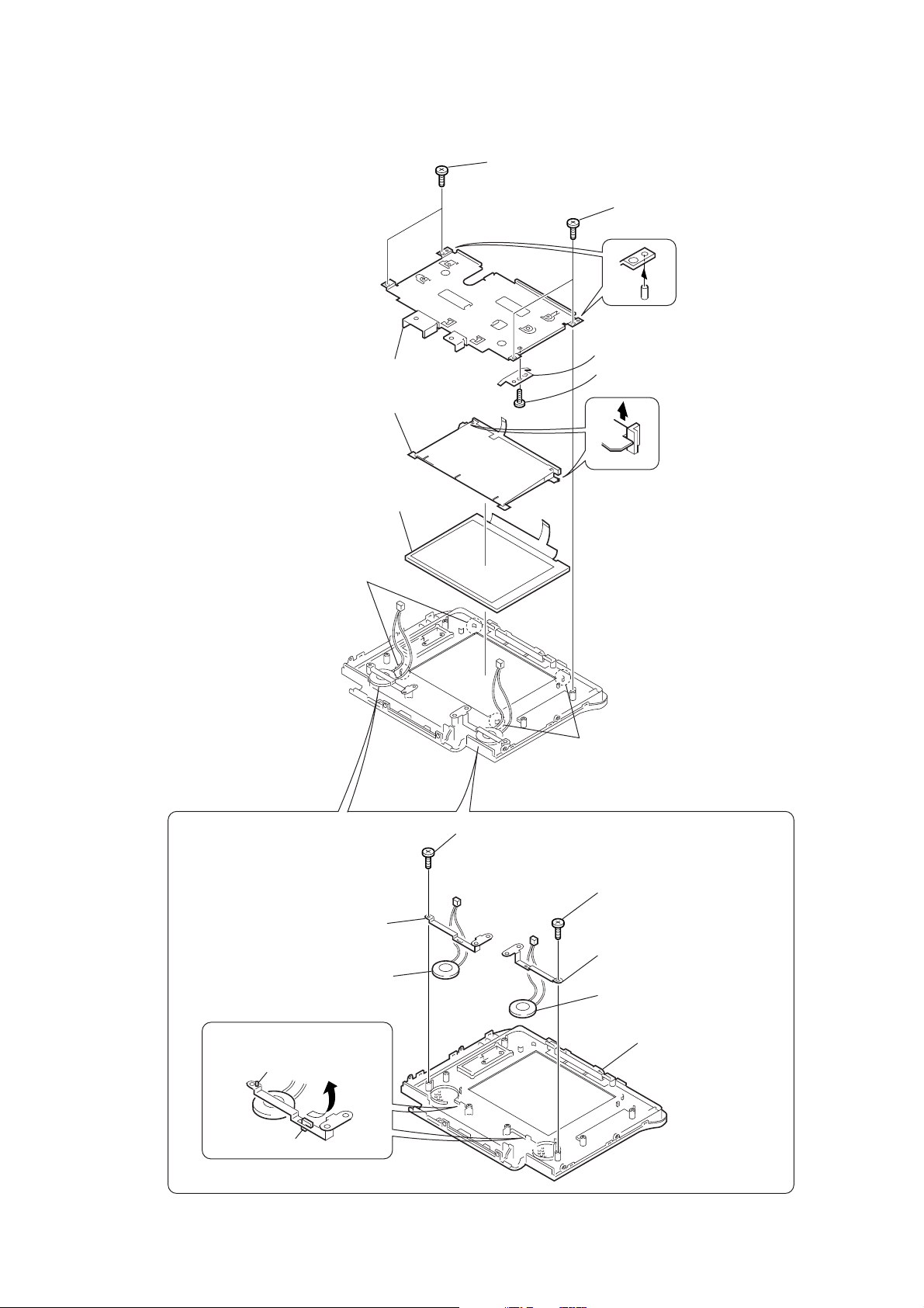
2-5. LCD WINDOW CABINET ASSEMBLY (SP-901, 902)(D800, D800E MODEL)
1
Two tapping screws
×
5)
2
Two tapping screws
(B2 × 5)
5
LCD ground plate
4
Screw (M2 × 3),
lock ace, p2
3
PD frame
6
LCD901
9
ND901
(B2
7
3
SP ground plate
4
Two claws
SP902
8
Two claws
REMOVING THE LCD WINDOW
CABINET ASSEMBLY (SP901, 902)
1
Tapping screw
×
(B2
5)
5
Tapping screw
×
(B2
6
5)
SP ground plate
7
SP901
2
Remove the SP ground plate
in the direction of the arrow.
Dowel
Claw
2-5
8
LCD window cabinet
assembly
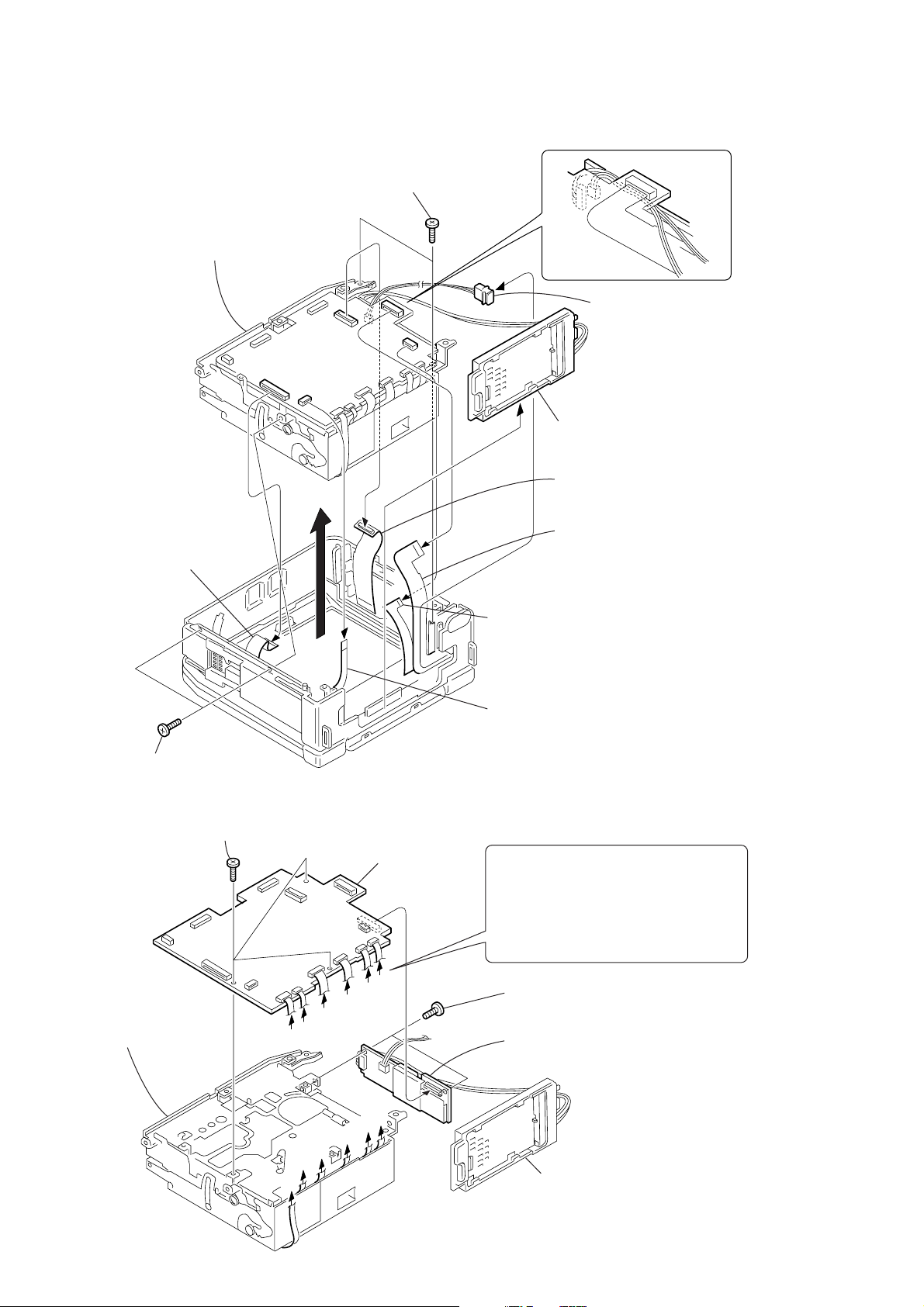
2-6. BATTERY PANEL ASSEMBLY, BATTERY TERMINAL BOARD, DC-IN CONNECTOR
7
Two tapping screws
×
5)
9
DC-IN connector (3P),
DC jack assembly
6
Battery panel assembly,
Battery terminal board
5
FP-247 flexible board
(50P)
3
FP-569 flexible board
(26, 32P)
0
Mechanism section
1
FP-570 flexible board
(40P)
(B2
Board
VC-250
8
Two screws (M2 × 4),
lock ace, p2
2-7. VC-250, FU-145 BOARDS
3
Three screws (M2 × 3),
lock ace, p2
VC-250
5
Mechanism deck
A
B
B
oard
C
D
E
4
VC-250 board
F
4
FP-572 flexible board
(6, 10P)
2
FP-602 flexible board
(5P)
A
Control switch block (FK-78) (10P)
B
Flexible board
(from loading motor, mode switch) (8P)
C
Flexible board (from video head) (16P)
D
Flexible board (from drum motor) (10P)
E
Flexible board (from capstan motor) (12P)
F
Flexible board (from S reel/T reel) (15P)
1
Two screws (M2 × 3),
lock ace, p2
2
FU-145 board
A
B
C
D
E
F
Battery panel assembly,
Battery terminal board
2-6
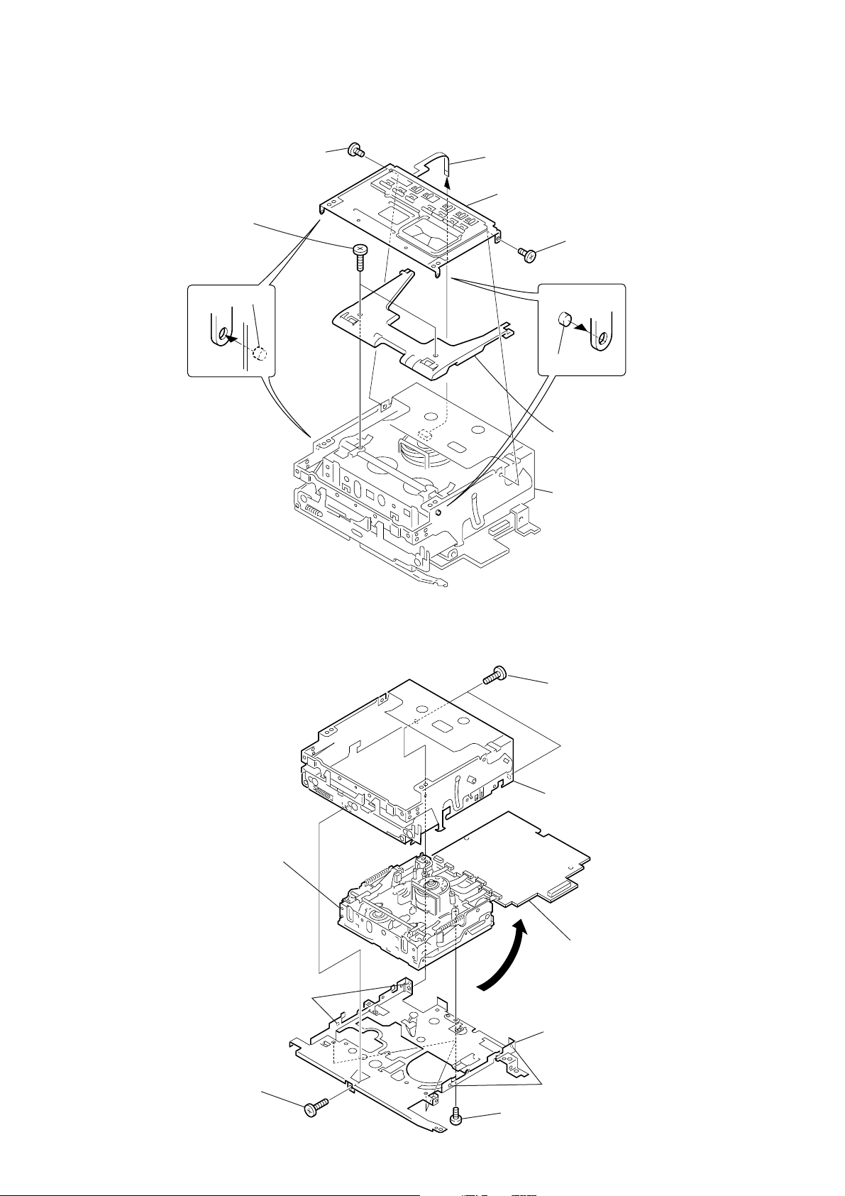
2-8. CONTROL SWITCH BLOCK (FK-78), LOADING LID
2
Screw (M1.4 × 1.6)
7
Two screws (M2 × 4),
lock ace, p2
4
Dowel
1
Remove the control switch block
(FK-78) (10P) in the direction of the arrow.
6
Control switch block
(FK-78) (10P)
3
Screw (M1.4 × 1.6)
5
Dowel
8
Loading lid
9
Mechanism deck
2-9. MECHANISM DECK, MAIN FRAME ASSEMBLY
9
Mechanism deck
3
Two dowels
Board
VC-250
1
Two screws (M2 × 3),
lock ace, p2
5
Lid frame assembly
6
Open the VC-250 board in the
direction of the arrow .
8
Main frame assembly
2
Screw (M2 × 3),
lock ace, p2
2-7
4
Two dowels
7
Three screws (M2 × 3),
lock ace, p2
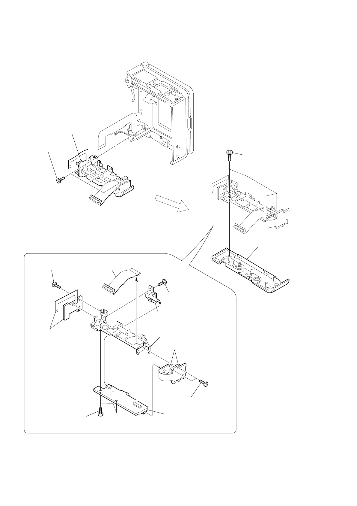
2-10.CABINET (R) BLOCK ASSEMBLY, JACK FRAME (IO-68, IR-38 BOARDS)
2
Cabinet (R)
block assembly
1
Three tapping
screws (B2
×
5)
3
Five tapping screws (B2 × 6)
REMOVING THE JACK FRAME
8
Screw (M2 × 3),
lock ace, p2
9
IR-38 board,
FP-572 flexible board
(6, 10P)
6
Three screws
(M2 × 4), lock ace, p2
5
board (50P)
IR-38
FP-247 flexible
IO-68
Board
3
Screw (M2 × 3),
lock ace, p2
4
FP-575 flexible board (6P)
0
Jack frame
2
FP-246 flexible
board (16P)
FP-246
1
Two screws (M2 × 3),
lock ace, p2
7
IO-68 board
4
Cabinet (R)
2-8
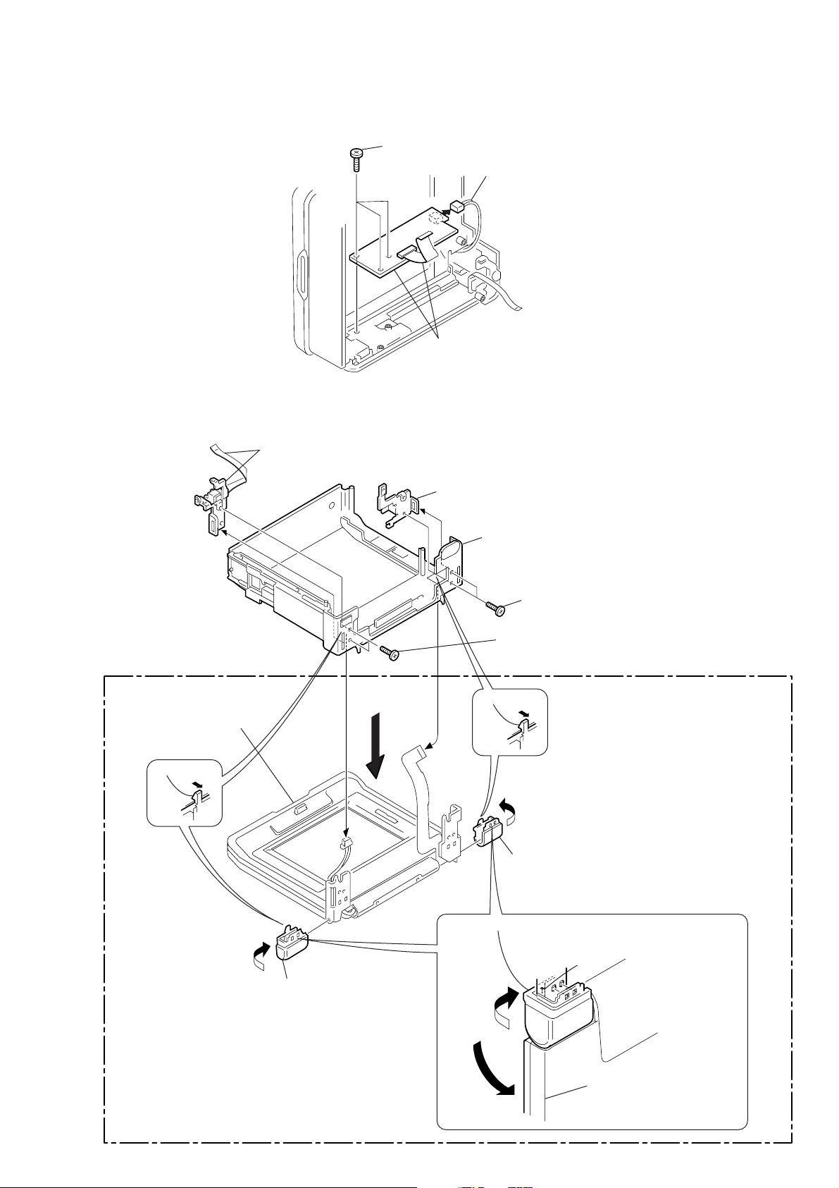
2-11.EX-36 BOARD, FP-570 FLEXIBLE BOARD
)
1
Three tapping screws (B2 × 5)
EX-36 board
3
EX-36 board,
FP-570 flexible board (40P)
2-12.UPPER CABINET ASSEMBLY,
LCD BLOCK ASSEMBLY (D800, D800E MODEL)
2
FP-602 flexible board (5P),
Strap sheet metal (L)
4
Strap sheet metal (R)
2
Harness (EP-51) (2P
(GV-D800/D800E model)
8
Remove the LCD block
assembly in the direction
of the arrow
6
A
Claw
5
Upper cabinet assembly
3
Two screws (M2 × 4),
lock ace, p2
1
Two screws (M2 × 4),
lock ace, p2
7
A
.
C
qa
Shaft cover (L)
Claw
D
qs
Shaft cover (R)
0
Remove the shaft cover (R), shaft cover
(L) in the direction of the arrow
Claw
CD
.
2-9
B
9
Open the LCD block
assembly in the direction
of the arrow
B
.
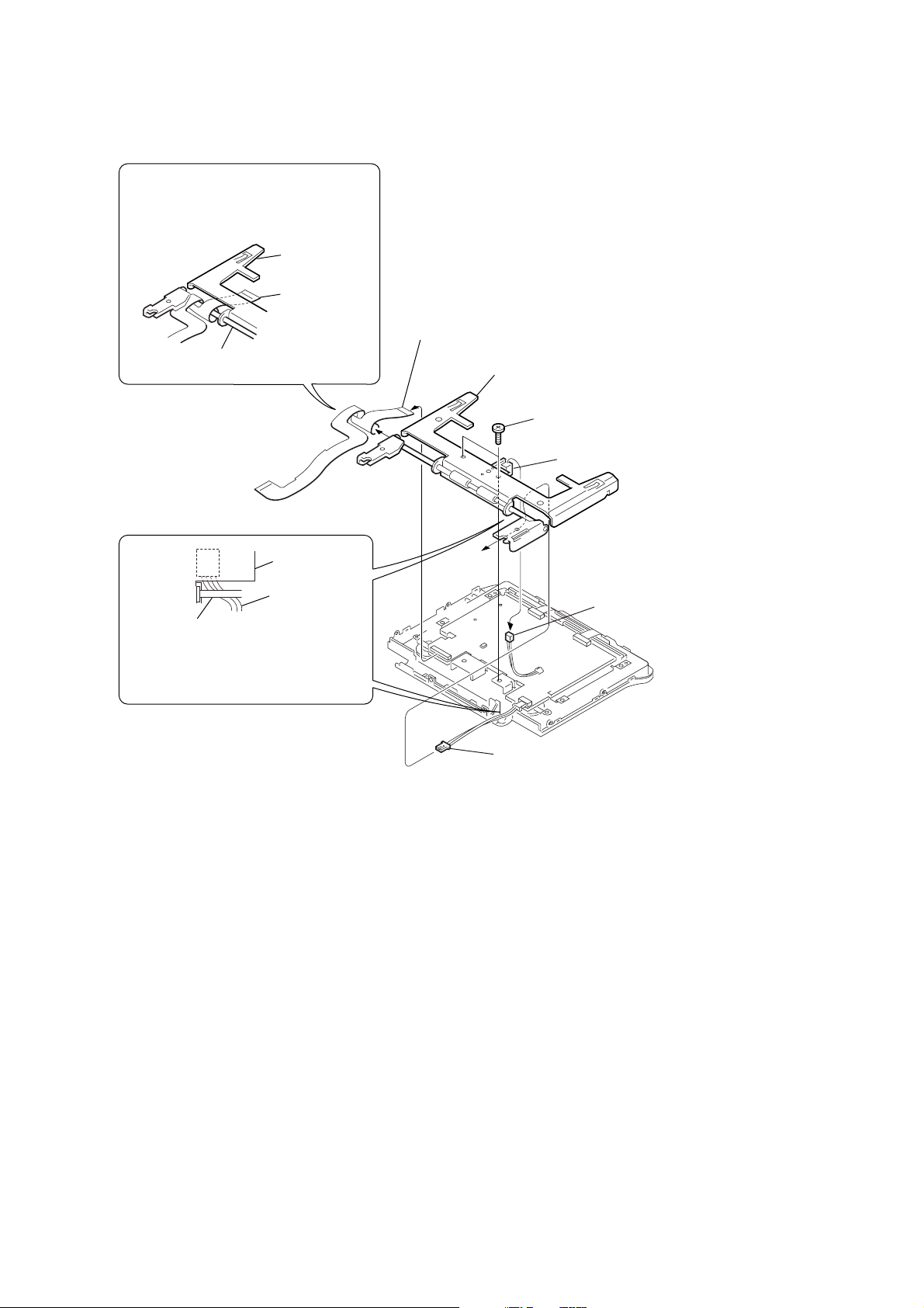
2-13.HINGE UNIT, FP-569 FLEXIBLE BOARD (D800, D800E MODEL)
When attaching the hinge unit, wrap the
FP-569 flexible board hinge shaft as shown
while taking care so that the flexible board
must not be caught or pinched.
Hinge unit
FP-569 flexible
board (26, 32P)
3
FP-569 flexible
Hinge shaft
Hinge unit
board (26, 32P)
4
Hinge unit
1
Two tapping screws
×
(B2
5)
LS-56 board
Harness
(EP-51) (2P)
Hinge shaft
When attaching the hinge unit, route the
harness through the notch as shown while
taking care so that the harness must not
be caught or pinched.
2
PD-130
Board
Harness (EP-51) (2P)
Harness (PL-53) (2P)
2-10
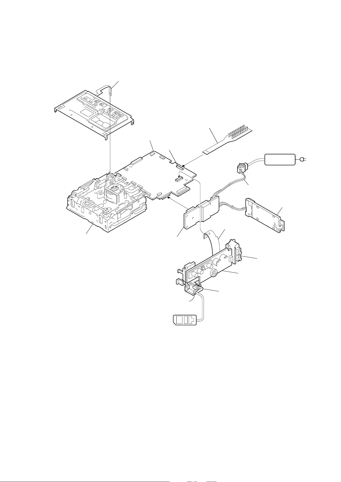
[CONNECTION DIAGRAM FOR SERVICE POSITION (Mainly for voltage measurement and check)]
(VC-250, FU-145, IO-68 BOARDS, MECHANISM DECK)
Control switch block
(FK-78) (10P)
CPC-13 jig
(J-6082-443-A)
VC-250 board
CN933
AC POWER
Mechanism deck
VC-250
Board
20
FU-145 board
ADAPTOR
1
DC-IN connector (3P),
DC jack assembly
Battery panel assembly,
Battery terminal board
FU-145
Board
FP-247 flexible
board (50P)
AC IN
LANC
jack
Adjustment remote
commander (RM-95)
IO-68
Board
FP-575 flexible
board (6P)
IO-68 board
FP-246 flexible
board (16P)
2-11
)
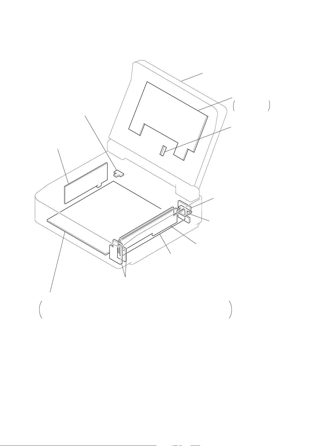
2-14.CIRCUIT BOARDS LOCATION
FP-602
(DV IN/OUT)
EX-36
(MULTI CONNECTOR)
LCD DISPLAY
MODULE
(D800/D800E ONLY)
PD-130
LCD DRIVER,
BACK LIGHT
LS-56
(LCD SWITCH
IR-38
(IR TRANSMITTER)
FP-575
(LANC)
FU-145
(DC/DC CONVERTER)
IO-68
(AV IN/OUT)
FP-246
(REMOTE COMMANDER RECEIVER)
VC-250
REC/PB AMP, DAC, DV INTERFACE, AD CONVERTER, Y/C PROCESSOR,
LINE A/D, LINE IN/OUT, IR, AUDIO IN/OUT, DRUM/CAPSTAN MOTOR DRIVE,
MECHA CONTROL, HI CONTROL, DC/DC CONVERTER
2-12
9
2
7
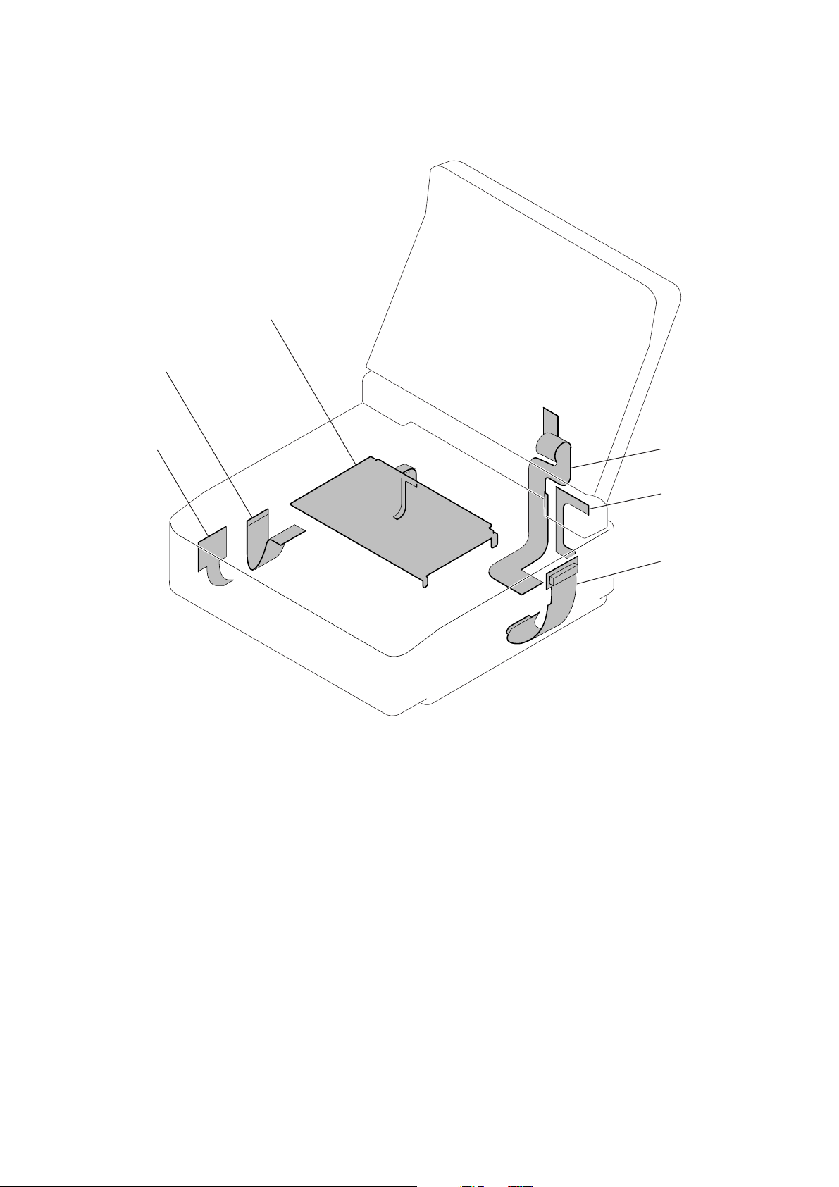
2-15.FLEXIBLE BOARDS LOCATION
The flexible boards contained in the mechanism deck are not shown.
CONTROL SWITCH BLOCK
(FK-78)
FP-570
FP-571
FP-56
FP-57
FP-24
2-13E
SECTION 3
BLOCK DIAGRAMS
GV-D200/D200E/D800/D800E
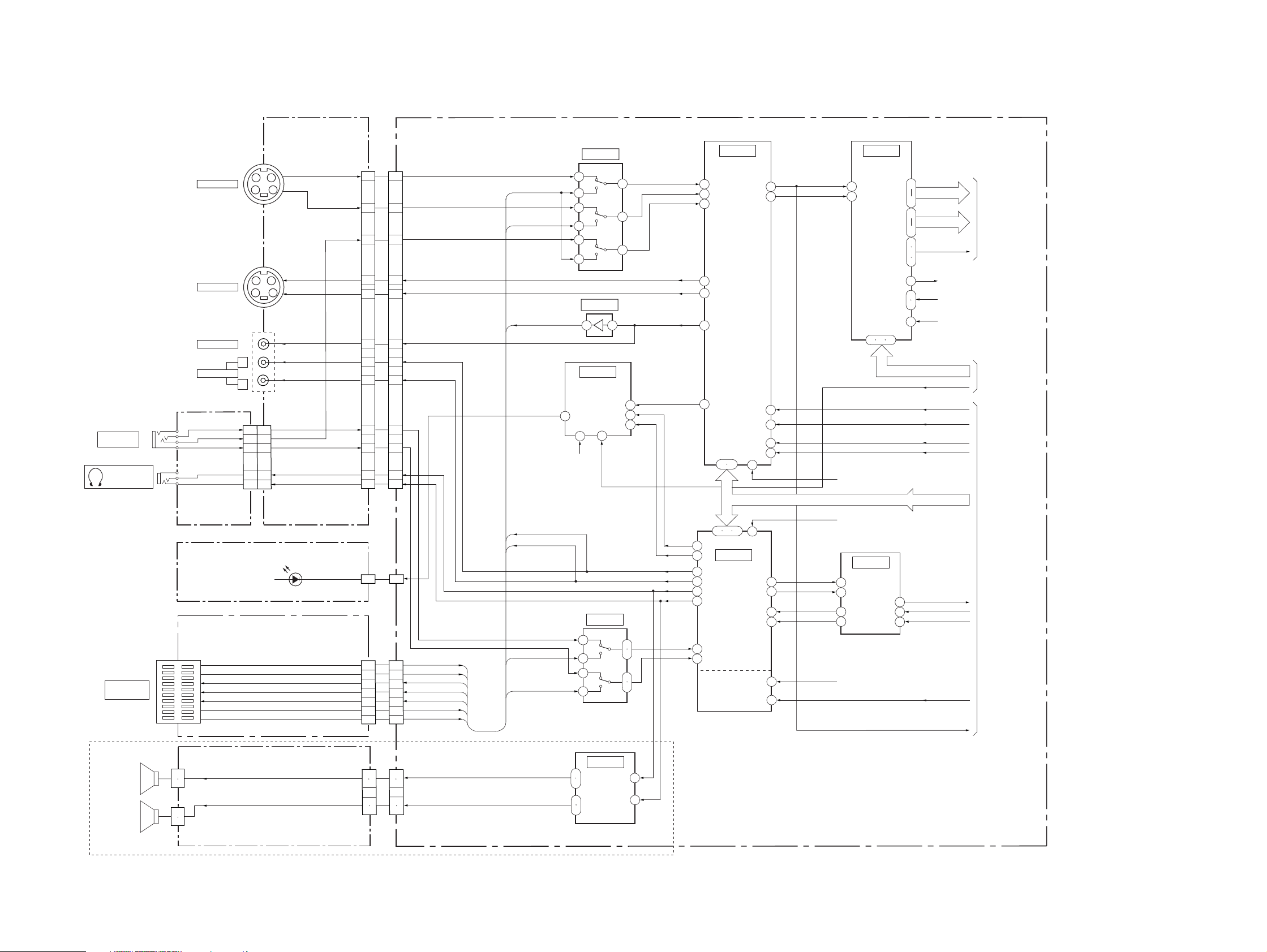
3-1. OVERALL BLOCK DIAGRAM (1/4)
(SEE PAGE 4-45)
IO-68 BOARD VC-250 BOARD(1/4)
(1/2)
13
1
2
5
7
CN104
L
V
R
HP L
HP R
Y
C
Y
C
V
L
R
J001
AUDIO/VIDEO
IN
J002
(HEADPHONES)
J101
S VIDEO IN
J103
S VIDEO OUT
VIDEO OUT
AUDIO OUT
J102
CN001
L
R
1
2
13
5
7
FP-246(1/2)
(FLEXIBLE)
(SEE PAGE 4-45)
IR-38 BOARD
(SEE PAGE 4-27)
D362,363
(SUPER LASER LINK)
EX-36 BOARD(1/2)
(SEE PAGE 4-63)
3
1
2
1
2
CN5505
20
1
15
14
6
5
PD-130 BOARD(1/3)
(SEE PAGE 4-55)
(GV-D800/D800E)
SPEAKER(L)
SPEAKER(R)
16
CN204
MULTI
CONNECTOR
SP901
SP902
( ) : Page No. shown in ( ) indicates the page to refer on the schematic diagram.
(4-25)
IC3702
CN924
29
31
35
19
17
15
11
9
37
39
43
41
43
CN922
EX Y/V IN
EX C IN
EX VIDEO OUT
EX AUDIO L OUT
EX AUDIO R OUT
22
IR FSC
(IC3301)
11
14
16
1
8
9
IC3703
1
(4-27)
IC3901
IR
TRANSMITTER
18
7
(4-31)
3
5
3
6
(4-25)
41
46
48
Y
C
V
Y
C
V
IR V
IR L
IR R
IR L
IR R
L
R
HP L
HP R
CN103
30
32
36
20
18
16
12
10
38
40
44
42
CN361
IC5703
CN203
CN5503CN5506
1
2
19
13
17
15
6
4
EX Y/V IN
2
EX C IN
19
EX VIDEO OUT
13
EX AUDIO L OUT
17
EX AUDIO R OUT
15
EX AUDIO L IN
6
EX AUDIO R IN
4
CN931
EX AUDIO L IN
EX AUDIO R IN
4
8
11
IC5704
25
26
1
2
SP L+,L-
SP R+,R-
CN923
2
1
26
25
13
16
7
4
SPEAKER
AMP
(4-31)
2
3
9
10
11
9
L
R
L
R
(4-26)
IC3701
(TAKO)
LINE IN
LINE OUT
39
AGC
48
ACC
42
18
14
22
24
910
20 21 22
55
56
IC5701
AUDIO
57
58
52
54
64
3
I/O
8mm
PB AUDIO
PROCESS
Y
36
C
34
46
7
44
5
11
23
4
5
7
8
14
26
L
R
L
R
(4-31)
(4-23)
IC3603
(ALIGN)
A/D
CONVERTER
2
6
66 64 63
XCS TAKO (IC4501)
XCS AU (IC4501)
(4-32)
IC5702
AUDIO
A/D CONV.
3
D/A CONV.
2
15
16
AFM FSC (IC2201)
59
Y0-Y7
52
49
C0-C7
42
38
HD,VD,DE
37
36
34
AFCK
68
SPCK
31
(IC1505)
XCS ALIGN
65
(IC4803)
HI SO,HI SI,XHI SCK
SIRCS PWM
CAIN Y
CAIN C
KINUTA Y
KINUTA C
VSP SO,VSP SI,XVSP,SCK
DATA TO SFD
8
DATA FROM SFD
9
12
SFD BCK
PB RF
TO
OVERALL
BLOCK(2/4)
(SEE PAGE 3-3)
TO
OVERALL
BLOCK(4/4)
(SEE PAGE 3-8)
TO
OVERALL
BLOCK(2/4)
(SEE PAGE 3-3)
Y
3-1 3-2
GV-D200/D200E/D800/D800E
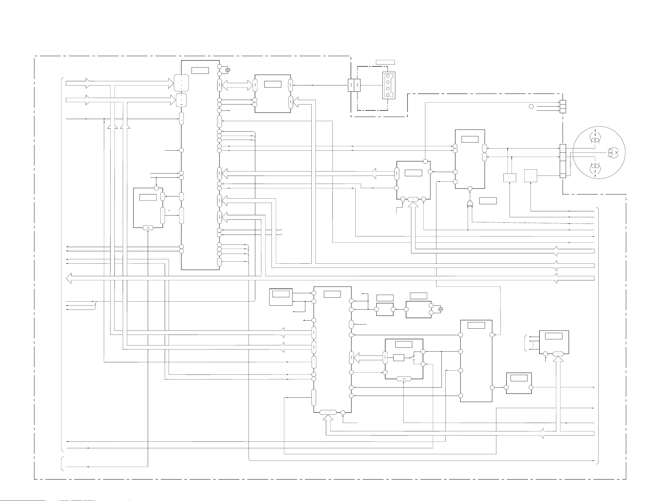
3-2. OVERALL BLOCK DIAGRAM (2/4)
VC-250 BOARD(2/4)
TO
OVERALL
BLOCK(1/4)
(SEE PAGE
3-2)
Y0-Y7
C0-C7
HD, VD, OE
CAIN Y
CAIN C
KINUTA Y
KINUTA C
Y0-Y7
C0-C7
HD,VD,OE
AFCK (IC2603)
SPCK (IC1505)
IC3302
CHARACTER
GENERATOR
(4-15)
13
XCS OSD
OSD SO
XOSD SCK
IR FCS
( ) : Page No. shown in ( ) indicates the page to refer on the schematic diagram.
(4-15)
IC3301
199 201
203 205
207 211
213 215
13
57
916
8
HD
VD
20
19
COL0
18
COL3
17
16
14
(CAIN)
DV SIGNAL
PROCESS
17
21
23
182
196
48
184
183
195
194
191
190
55
59
138
X3301
24.576MHz
139
142
L BUS
145
TRCK
51
LCK
141
VREF
151
152
PRRV,TRRV,TRRT
153
156
DATA TO SFD
133
DATA FROM SFD
132
127
99
97
83
88
81
79
170
179
159
161
163
162
75
73
71
105
106
SFD BCK
6 6
MC BUS
VSP SO, SI, SCK
PANEL G
PANEL R
PANEL B
PANEL HD,VD
45
42
47
79
(4-17)
IC3303
(LIP)
DV INTERFACE
TPA+,-
6
TPB+,-
9
29
MC BUS
37
XCS SFD (IC4501)
XCS VFD (IC4501)
CN929
REC CK
REC DT
AD DT
6
PB CK
ATF ERR
CN1104
2
4
5
1
FP-602
(FLEXIBLE)
(SEE PAGE 4-17)
CN1105
DV IN/OUT
AD DT
PB CK
15
20
13
XCS TRF
(IC4501)
(4-11)
IC3101
(TRF)
EQ
A/D CONV.
PLL
25 31
22 24
RF MON
16
CN933(1/2)
PB RF (IC3202 )
AFC FO (IC2201)
14
(4-12)
IC3103
40
42
27
29
(TRW)
REC/PB
AMP
35
4
12
6
7
2
1
Q3107
Q3109,3110
Q3112-3115
IC3102
(4-11)
ODD
EVEN 12
Q3104,3108
Q3111,3116
FLYING
FILTER
SW
ERASE
OSC
REC CK
REC DT
34
PB Y OUT
42
DV PB RF
CN3101
FOR
5
ADJUSTMENTS
2
10
9
13
16
ERRV,TRRV,TRRT
DRP SO,XDRP SCK
(SEE PAGE 4-11)
XFE ON
DRUM 8PB
VC RF SWP
DV RF SWP
ATF ERR
MC BUS
DRUM
ODD
EVEN
FLYING
ERASE
TO
OVERALL
BLOCK(4/4)
(SEE PAGE 3-8)
16
DATA TO SFD
DATA FROM SFD
SFD BCK
PB RF
Y
XCS OSD
OSD SO
XOSD SCK
(4-21)
OSCI
IC2202
VCO (KINUTA)
AFC FO
AFM FSC
Y0-Y7
C0-C3
HD,VD,OE
Y
C
MECHA HD
MECHA VD
MECHA FLD
TBC VD
AMPO
67
53
79
139
122
112
199
146
144
142
4
213
93
94
89
168
(4-21)
IC2201
HI8/STD8
PB Y/C
PROCESS
9695 97
VSP SO,VSP SI,XVSP SCKVSP SO,VSP SI,XVSP SCK
9
7
DV PB RF
(4-13)
IC3201
HI8/STD8
PB RF
AMP
TO
OVERALL
BLOCK(3/4)
(4-13)
18
ADJUSTMENT
VOLTAGE
(4-13)
IC2291
3
DA STB
(IC4902)
D/A CONV.
(EVR)
12
(SEE PAGE
3-5)
IC3202
RF ENV
DET
3
5
4
RF ENV DET
MECHA HD
MECHA VD
MECHA FLD
TBC VD
XCS CH
CH SO
XCH SCK
VC SO,VC SI,XVC SCK
PANEL R
PANEL G
PANEL B
PANEL HD,VD
4
IC1502
A/D
REC
(4-19)
46 48
(4-19)
IC1504
27MHz
PB
XTAL
OSC
X1501
27MHz
4
2
PB C RF
36
34
PB RF
DOP
11
14
SPCK
SPCK
81
VCK
198
101
100
RF AGC OUT
51
196
187
AD CK
185
PB C RF
49
77
98
XCS KINUTA(IC4902)
(4-19)
IC1505
5 1
CK CONT 1,2(IC4902)
AD1-AD10
1/2
2
11
16
3-3 3-4
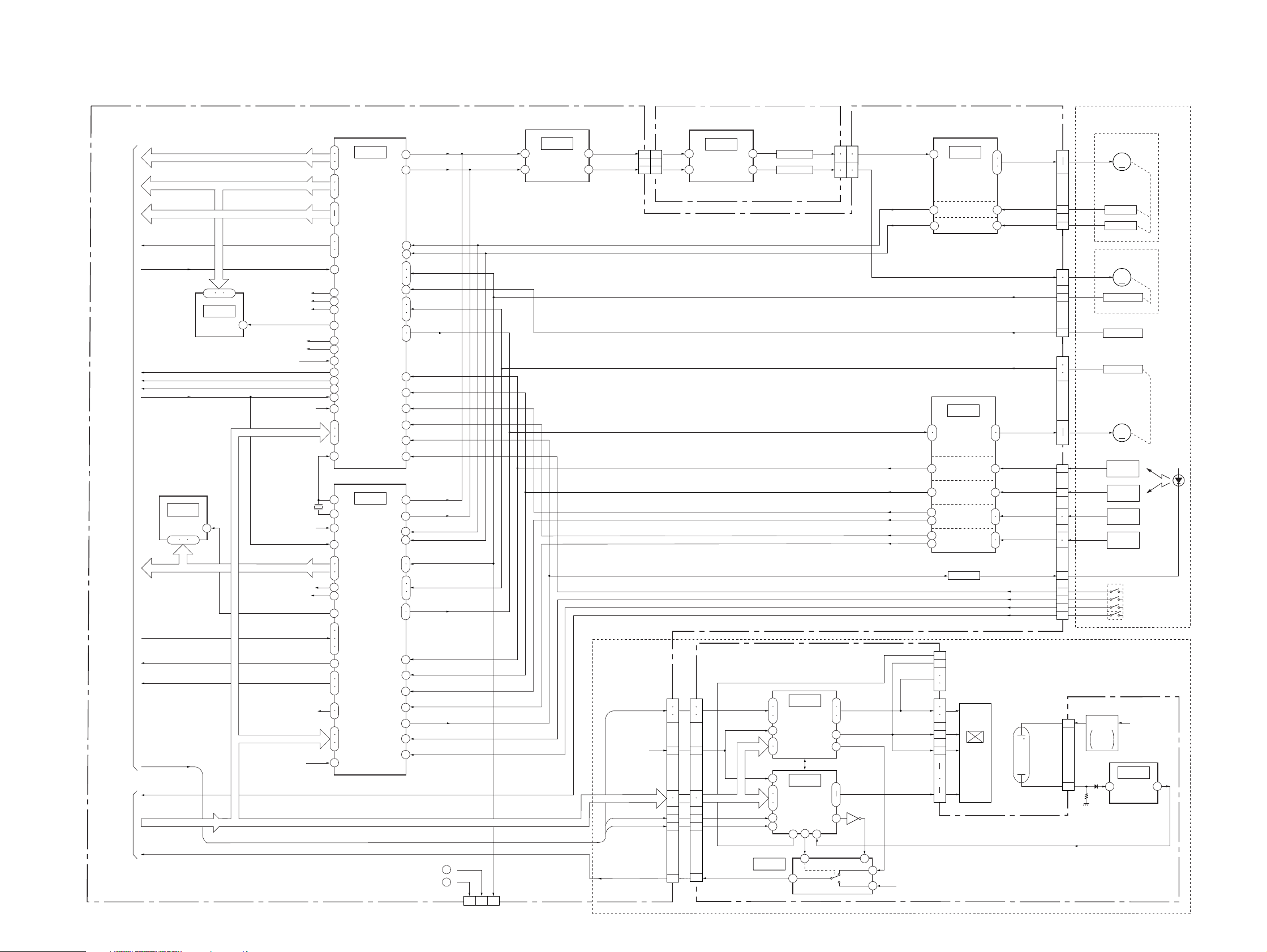
GV-D200/D200E/D800/D800E
3-3. OVERALL BLOCK DIAGRAM (3/4)
VC-250 BOARD(3/4)
DRP SO,DRP SI,XDRP SCK
VSP SO,VSP SI,XVSP SCK
MC BUS
FRRV,TRRT,TRRV
ATF ERR
XCS VFD (IC3301)
XCS SFD (IC3301)
XCS TAKO (IC3701)
XCS EEP
1
XCS AU (IC5701)
XCS TRF (IC3101)
VREF (IC3301)
XCS MECHA (IC4803)
HI SO,HI SI,XHI SCX
LINE OUT V (IC3301)
XCS KINUTA (IC2201)
DA STRB (IC2291)
CK CONT 1,2 (IC2201)
HI SO,HI SI,XHI SCX
XCS VC (IC4803)
X4901
20MHz
XCS EEPROM
16
TO
OVERALL
BLOCK(2/4)
(SEE PAGE
3-4)
TO
OVERALL
BLOCK(4/4)
(SEE PAGE
3-8)
32 4
IC4502
EEPROM
(4-36)
DV RF SWP
XFE ON
DRUM 8 PB
RF ENV DET
(4-29)
IC4901
EEPROM
1
32 4
VC SO,VC SI,XVC SCX VC SO,VC SI,XVC SCX
MECHA FLD
MECHA HD
MECHA VD
TBC VD
VC RF SWP
XCS CH,CH SO,XCH SCK
PANEL R
PANEL G
PANEL B
PANEL HD,VD
XCC DOWN
HI SO,HI SI,XHI SCK
BL CONT
( ) : Page No. shown in ( ) indicates the page to refer on the schematic diagram.
(4-35)
78
IC4501
79
80
DIGITAL8
MECHA
74
CONTROL
SIGNAL
75
PROCESS
76
CONTROL
26
38
106
107
108
95
17
28
18
88
21
23
112
62
59
111
99
72
81
82
83
1
DRUM PWM DRUM PWM
68
CAP PWM
69
DRUM FG
116
DRUM PG
117
115
CAP FG
110
109
DEW DET
96
39
MODE SW A-C
40
41
LOAD
UNLOAD
49
50
TAPE END
54
TAPE TOP
53
T REEL FG
114
S REEL FG
113
TAPE LED ON
55
REC PROOF
44
CAP PWM
(4-33)
IC4401
28
25
(3/3)
LPF
DRUM ERROR
29
CAP ERROR
27
(4-29)
2
IC4902
HI8/STD8
1
MECHA
CONTROL
114
39
78
79
80
19
21
27
111
112
113
118
47
83
82
81
104
110
74
75
76
78
DRUM PWM
69
CAP PWM
68
DRUM FG
116
DRUM PG
117
CAP FG
115
109
35
MODE SW A-C
36
37
LOAD
UNLOAD
32
33
TAPE END
42
TAPE TOP
41
T REEL AFG
96
S REEL AFG
95
TAPE LED ON
31
ME SW
38
HI8 MP SW
40
DV RF SWP (IC4501 )
VC RF SWP (IC4902 )
62
47
8 13 15
CN933(2/2)
FOR ADJUSTMENTS
PANEL R
PANEL G
PANEL B
XCS LCD
(IC4803)
HI SO,XHI SCK
PANEL HD
PANEL VD
BL CONT
FU-145 BOARD(1/2)
IC1301
15
9109
10
11
CN1301CN921
PD-130 BOARD(2/3)
5
22
6
21
7
20
14
13
13
14
15
12
10
17
11
16
23
4
CN923
CN5503
PWM
DRIVE
(4-49)
HD OUT
(1/2)
(4-57)
58
64
IC5601
48
47
46
41
40
39
44
46
45
42
1
48
Q1306
SWITCHING
SWITCHING
Q1305
GENERATOR
CN1301
RGB
20
22
24
27
35
10
24
IC5501
DRIVE
(4-55)
IC5502
TIMING
(4-55)
8
2 5
5 2
1
3
4
1
2
9
CN921
3
4
1
2
VR,VG,VB
COM
DA
Q5601
DRUM YS
DRUM FG
DRUM PG
LOAD
UNLOAD
TAPE END
TAPE TOP
T REEL FG
T REEL AFG
S REEL FG
S REEL AFG
TAPE LED ON
HD OUT
PANEL COM
VR,VG,VB
VCOM
VGLAC
CN5501
7
6
PANEL 2.8V
3-5 3-6
(4-33)
IC4401
6
(1/3)
DRUM
MOTOR
DRIVE
FG AMP
16
PG AMP
22
(4-33)
IC4401
LED DRIVE
8
4
CN5502
FOR
5
ADJUSTMENTS
3
1
19
20
21
11
4
5
10
12
18
(2/3)
LOADING
MOTOR
DRIVE
TAPE END
DETECT
TAPE TOP
DETECT
T REEL
FG AMP
S REEL
FG AMP
Q4401
LCD
UNIT
55
56
47 46
44
41
39
33
34
61
59
57
17
20
53
51
45
38
39
36
35
MODE SW A-C
LM(+),LM(-)
TAPE END(C)
TAPE TOP(C)
T REEL(+),(-)
S REEL(+),(-)
REC PROOF
HI8 MP SW
XCC DOWN
ND901
BACKLIGHT
CN4402
U, V, W
CN4403
CAP VS
CAP FG
DEW DET
CN4401
ME SW
CN4404
BL HIGH
BL LOW
CN5604
B710-MECHA DECK
(SEE PAGE 4-56)
M901
10
5
3
1
8
7
1
12
2
3
4
5
8
8
2
12
11
5
4
14
7
6
3
15
10
DRUM MOTOR
DRUM FG
DRUM PG
CAPSTAN MOTOR
CAPSTAN FG
DEW SENSOR
MODE SWITCH
LOADING MOTOR
Q002
TAPE END
Q001
TAPE TOP
S001
S002
T5601
Q5602
INVERTER
BACK
LIGHT
DRIVE
M
M902
M
S901
M903
M
SENSOR
SENSOR
T REEL
SENSOR
S REEL
SENSOR
IC5602
CURRENT
3
3
BL DET
REC PROOF
ME/MP
HI8 MP
CC DOWN
BL REG
(4-57)
DET
D001
TAPE
H001
H002
(GV-D800/D800E)
4
LED
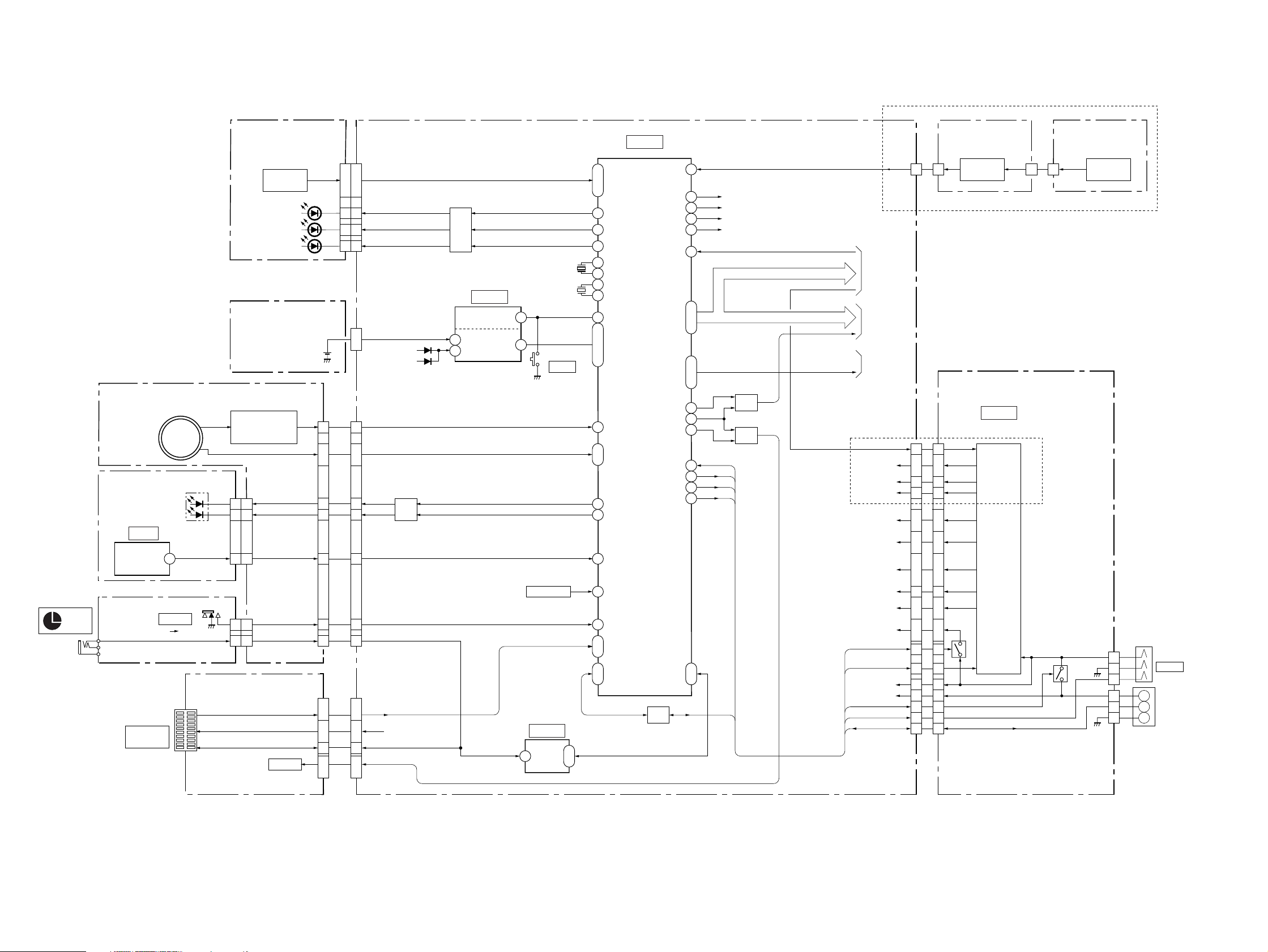
GV-D200/D200E/D800/D800E
3-4. OVERALL BLOCK DIAGRAM (4/4)
FK-78 BOARD VC-250 BOARD (4/4)
(SEE PAGE 4-61)
S001–016
FUNCTION
SWITCH
D001 (REC)
D002 (PAUSE)
D003 (CAUTION)
(SEE PAGE 4-37)
FP-571
(FLEXIBLE)
VANADIUM
LITHIUM
BATTERY
IO-68 BOARD (2/2)
S101, 102, 104, 105
EXEC
S. LASER LINK SW
CN001
8
10
14
121
VOLUME SW
MENU SW
CN104
X POWER LED
8
X CHARGE LED
10
SIRCS SIG
14
LANC SIG
2
CN105
J001
(LANC)
(SEE PAGE 4-45)
S103
FP-246 (2/2)
(FLEXIBLE)
COMMANDER
(SEE PAGE 4-45)
(POWER)
(CHARGE)
IC001
REMOTE
RECEIVER
FP-575
(FLEXIBLE)
OFF ON
(SEE PAGE 4-45)
SEL/PUSH
EXEC
DIAL
1
S001
POWER
D001
EX-36 BOARD(2/2)
CN204
MULTI
CONNECTOR
11, 17
18, 19
8
(SEE PAGE 4-65)
16
BZ201
BUZZER
( ) : Page No. shown in ( ) indicates the page to refer on the schematic diagram.
CN001
6
BT001 1
CN103 CN922
23
26
•
25
46
43
45
2
1
10
•
11
23
|
CN203
26
8
39
•
40
LANC SIG
6
•
•
5
5
•
•
7
7
2
2
4
4
3
3
CN926
•
2
24
25
•
26
45
44
46
1
2
10
•
11
23
|
26
8
39
•
40
X REC LED
X PAUSE LED
X CAUTION LED
BATT LI 3V
VTR UNREG
BATT UNREG
Q4808–4810
DRIVE
EX UNREG
BEEP
CN931
LED
Q906–908
LED
DRIVE
3
7
(4-37)
IC4801
RESET
VDD SWITCH
LANC SIG
5
6
IC4802
X4801
20MHz
X4802
32.768kHz
S4801
RESET
S4802
EJECT SW
(4-37)
LANC I/O11
93
•
94
•
95
6
8
55
40
41
52
53
38
42
•
51
•
77
•
87
98
67
•
68
5
57
4
17
14
72
•
73
48
•
49
10
•
12
(4-37)
IC4803
HI CONTROL
KEY AD0
KEY AD1
KEY AD2
X REC LED
X PAUSE LED
X CAUTION LED
20MHz OUT
20MHz IN
32kHz IN
32kHz OUT
XRESET
VDD
KEY AD5
DIAL A
DIAL B
X POWER LED
X CHARGE LED
SIRCS SIG
X EJECT SW
X VTR MODE SW
ID1
ID2
IB SI
IB SO
XCS MECHA
XCS ALIGN
XOSD SCK
SIRCS ENV
MELODY ENV
BATT/EXT SW
FAST CHARGE
VTR DO ON
LANC OUT
Q4804
XCS VC
XCS LCD
HI SO
HI SI
HI SCK
XCS OSD
OSD SO
MELODY
SHOE ON
LANC IN
IF
99KEY AD6
80
3
58
27
18XCC DOWN
33
•
34
•
35
44
•
45
•
46
59
36
56
66
50
29
81
1
•
2
BATT SIG
XCS MECHA (IC4501)
XCS VC (IC4902)
XCS ALIGN (IC3603)
XCS LCD (IC5501, 5502)
HI SO, HI SI, XHI SCK
HI SO, HI SI, XHI SCK
Q4802, 4805
MOD
Q4803
MOD
XCC DOWN
BL CONT
SIRCS, PWM
XCS OSD
OSD SO
XOSD SCK
(GV-D800/D800E)
CN923
TO
OVERALL
BLOCK(3/4)
(SEE PAGE
3-5)
TO
OVERALL
BLOCK(1/4)
(SEE PAGE
3-2)
TO
OVERALL
BLOCK(2/4)
(SEE PAGE
3-3)
(GV-D800/D800E)
BL CONT
BL REG
PANEL –15V
PANEL 13V
1.5V
2.8V
4.75V
RP UNREG
MT 5V
EX UNREG
SHOE ON
VTR DO ON
VTR UNREG
BATT UNREG
PD-130
LS-56 BOARD
BOARD (3/3)
S5601, 5602
23 4 11
LCD BRIGHT
CN5503
(SEE PAGE 4-57)
AD6
SW
CN001CN5608
(SEE PAGE 4-56)
FU-145 BOARD (2/2)
(4-49)
IC1301
DC-DC CONVERTER
(2/2)
42
42
46
46
•
•
45
45
44
44
43
43
26
26
•
•
25
25
22
22
|
|
19
19
16
16
•
•
15
15
•
•
14
14
13
13
8
8
•
•
7
7
32
•
31
30
29
35
36
39
38
37
Q507
VTR UNREG
BATT UNREG
FAST CHARGE
BATT/EXT SW
BATT SIG
CN1301CN921
32
•
31
30
29
35
36
39
38
37
Q502
S001
LCD ON/OFF
SW
CN502
CN501
+
S
–
J902
DC IN
J901
BATTERY
TERMINAL
1
2
3
1
5
4
3-7 3-8
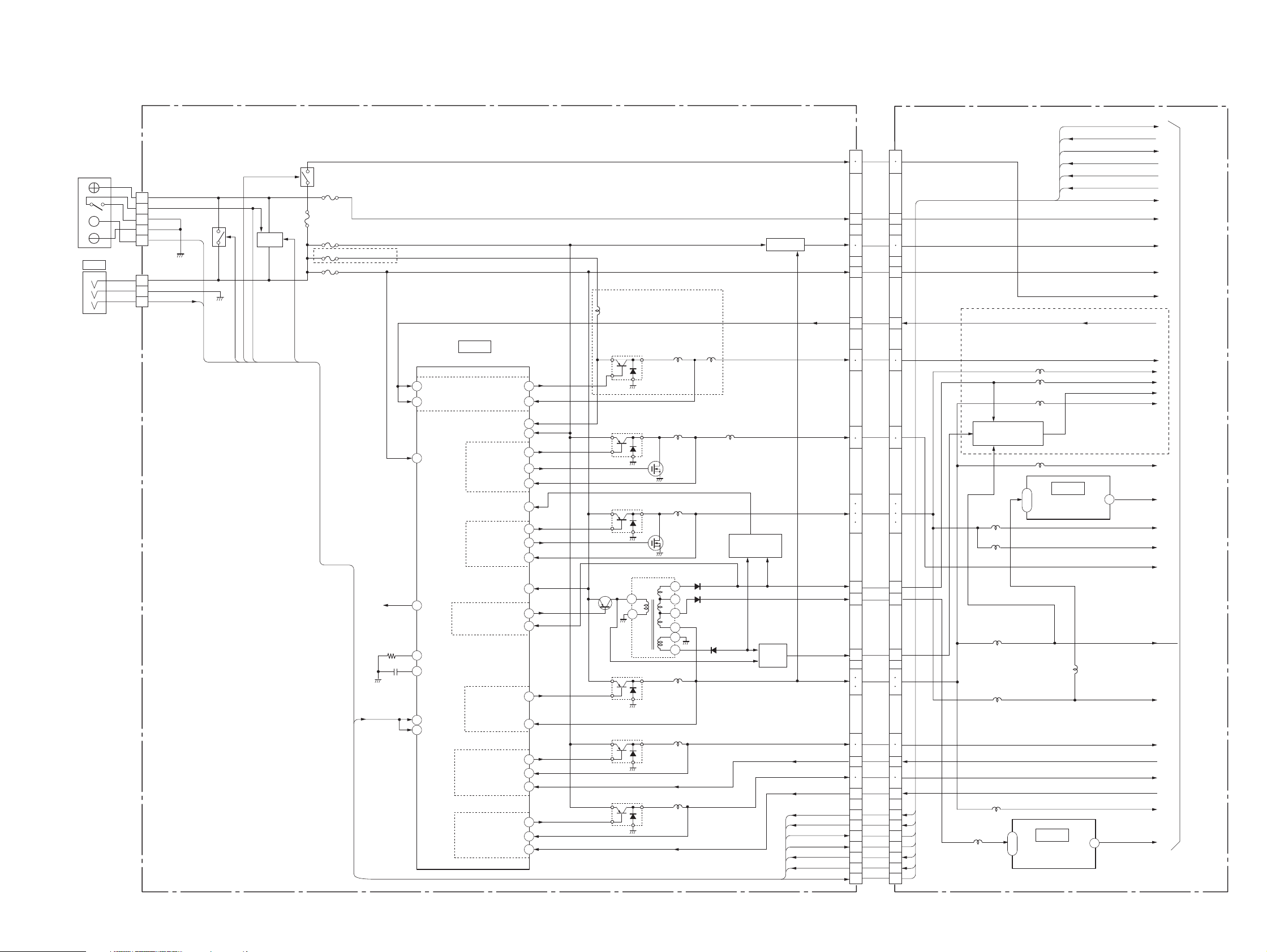
GV-D200/D200E/D800/D800E
S
7
31
28
2
6
5
1
57
54
18
41
45
42
40
49
50
34
27
6
7
2
3
46
37
21
22
29
30
64
10
11
58
14
15
1
4
5
8
4
3
1
2
3
4
5
1
2
3
1
5
IC1301
IC1303
IC1302
J901
BATTERY
TERMINAL
J902
DC IN
CN501
BATT (+)
BATT SW(+)
BATT SW(–)
BATT(–)
BATT SIG
Q501,
502
Q506,
507
ACV UNREG
BATT/XEXT SW
CN502
FAST CHARGE
SHOE ON
DC PACK SW
F501
F502
F504
F505
F503
Q503–505
CHARGE
SWITCH
INIT CHARGE ON
(GV–D800/D800E)
C/D VS D1.5V
BL UNREG
VTR UNREG
BL CONT
VC–250 BOARD(1/2)FU–145 BOARD
DC/DC CONVERTER
(4–39)
(4–39)
(4–49)
NONINV
INPUT–7
STANDBY–7
OUTPUT–7
MONITOR-7
OUTPUT
OUTPUT VCC–7
OUTPUT VCC–4,5,6
OUTPUT–4
MOS GATE–4
OUTPUT
MONITOR–4
OUTPUT–1
MOS GATE–1
OUTPUT
MONITOR–1
VCC
COMP
VREF
VTR DD ON
16
VREF
OUTPUT VCC–1,2,3
OUTPUT–3
OUTPUT MONITOR–3
RT
CT
OUTPUT–2
OUTPUT
MONITOR–2
OUTPUT–6
OUTPUT MONITOR–6
NONINV INPUT–6
OUTPUT–5
OUTPUT MONITOR–5
NONINV INPUT–5
STANDBY–3
STANDBY
VTR DD ON
SHOE ON
BATT SIG
BATT/XEXT SW
FAST CHARGE
INIT CHARGE ON
DC PACK SW
29
30
37
38
39
40
41
29
30
37
38
39
40
41
1
2
10
3
4
9
1
2
10
3
4
9
44 44
14
15
16
43
13
43
13
19
20
21
22
19
20
21
22
2.8V
PANEL 13V
RP UNREG
25
26
25
26
1.5V
BL CONT
BL REG
BATT UNREG
MT 5V
VTR UNREG
42
45
46
42
45
46
31
32
36
7
8
35
31
32
36
7
8
35
CAP VS
CAP ERROR
DRUM VS
DRUM ERROR
PANEL –15V
4.75V
5.9V
REG
2
5
BL REG
PANEL 2.8V
PANEL 13.3V
PANEL –15.3V
PANEL 4.75V
A 4.75V
A 2.8V
AU 2.8V
D 1.5V
D 1.9V
1.9V REG
TO
POWER
BLOCK(2/2)
L1313
AV 4.75V
(GV–D800/D800E)
–15.3V
REG
L1309
L1320
L1315
Q1322,1324,1326
L1311
L1316
CAP VS
CAP ERROR
DRUM VS
DRUM ERROR
RP 4.75V
RP 6.0V
L1314
L1306
L1321
D 2.8V
L1307
L1308
Q1303
SWITCHING
Q1308
SWITCHING
Q1307
SWITCHING
Q1304
SWITCHING
Q1301
SWITCHING
Q1302
SWITCHING
Q1305
SWITCHING
Q1306
SWITCHING
L1305 L1310
L302
T1301
Q1314
D1302 (1/2)
RECT
D1306
RECT
D1302
RECT
EMERGENCY
DETECT
RECT
D1301,305
L1301
L1303
L1304
CAP VS
CAP ERROR
DRUM VS
DRUM ERROR
BATT UNREG
(GV–D800/D800E)
L501
L1317
L1318
Q1309
SWITCHING
EX UNREG
DC PACK SW
SHOE ON
BATT SIG
INIT CHARGE ON
VTR DD ON
FAST CHARGE
BATT/XEXT SW
BATT UNREG
MT 5V
VTR UNREG
EX UNREG
BL CONT
CN921
CN1301
5V REG
Q1310–1313
EX UNREG
14
15
16
(SEE PAGE
3-11)
3-5. POWER BLOCK DIAGRAM (1/2)
( ) : Page No. shown in ( ) indicates the page to refer on the schematic diagram.
3-9 3-10
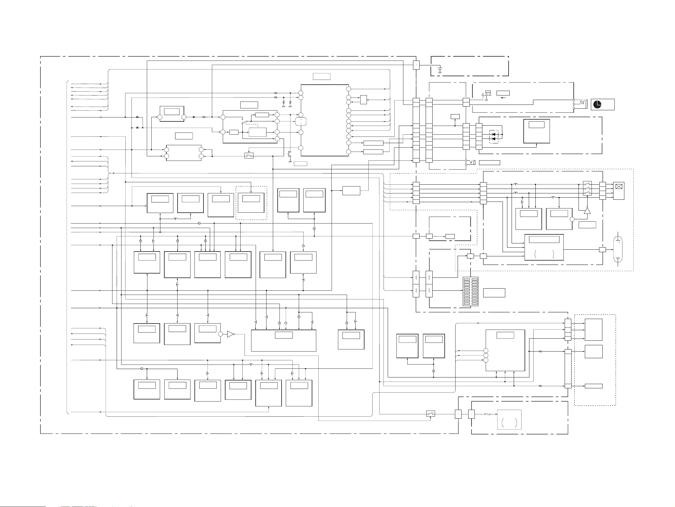
GV-D200/D200E/D800/D800E
3-6. POWER BLOCK DIAGRAM (2/2)
VC-250 BOARD(2/2)
DC PACK SW
SHOE ON
BATT SIG
INIT CHARGE ON
VTR DD ON
FAST CHARGE
16
TO
POWER BLOCK
(1/2)
(SEE PAGE
3-10)
BATT XEXT SW
BATT UNREG
MT 5V
VTR UNREG
EX UNREG
BL CONT
BL REG
PANEL 2.8V
PANEL 13.3V
PANEL -15.3V
PANEL 4.75V
AU 4.75V
D 1.9V
A 2.8V A 2.8V
AU 2.8V
D 1.5V
A 4.75V A 4.75V
D 2.8V D 2.8V
CAP VS
CAP ERROR
DRUM VS
DRUM ERROR
RP 4.75V
RP 6.0V
D4802
D4801
VTR UNREG
MT 5V
AU 4.75V
AU 2.8V
D 2.8V
FB3601
L3602
IC3603
(ALIGN)
A/D CONV.
A 2.8V
MT 5V
D 1.5V
L3707
IC3703
VIDEO OUT
AMP
RP 4.75V
A 2.8V
D 2.8V
FB1501
IC1504
XTAL
OSC
(4-19) (4-19)
LANC DC
IC5701
AUDIO I/O
(4-23)
(4-25)
( ) : Page No. shown in ( ) indicates the page to refer on the schematic diagram.
(4-37)
IC4803
HI CONTROL
INIT CHARGE ON
XVTR MODE SE
XCHARGE LED
FB4501
L2201-2203,
L2208
SHOE ON
IB SO
IB SI
VTR DD ON
FAST CHARGE
CHARGE INH
BATT/XEXT
XPOWER LED
FB1504
(4-37)
IC901
REG
1
14
(4-31)
FB3701
L3701,
3705
L3706
IC4802
LANC I/O
UNREG
LANC DC
L5701
IC3701
(TAXO)
VIDEO
LINE IN/OUT
AMP
(4-26)
IC3702
VIDEO
INPUT
SELECT
(4-25)
IC1505
FREQUENCY
DIVIDER
IC4801
D901
3 32
Q4806
IC5704
SPEAKER
(GV-D800/D800E)
REG 1.5V
(LIP)
DV
(4-17)
IR DRV
RF ENV
DET
(4-14)
AMP
L2209
L3102
BATTER IN
DETECT
(4-31)
L2204
REG
DV
7
(4-31)
IC5703
AUDIO
INPUT
SELECT
IC3303
INTERFACE
POWER
VCC
IC5702
AUDIO
ADC&DAC
(4-37)
(4-31)
FB3303
FB3370
4
8
IC3301
(CAIN)
SIGNAL
PROCESS
(4-15)
L3901
(4-27)
IC3901
TRANSMITTER
L3201 L3104 L3103
IC3201
IR
HI8/STD8
PB RF
AMP
24
Q3903
IC3202
(4-13)
(4-37)
RESET
CHARACTER
IC3103
(TRW)
REC/PB
5
6
4
8
EVER 3.0V
IC3302
GENERATER
(4-15)
FB2202
IC2201
RF 1.9V
AMP
42 51
86 87
S4801
RESET
(4-36) (4-35)
IC4502
EEPROM
IC2291
D/A CONV.
L2291
FB2204
HI8/STD8
PB Y/C
PROCESS
IC3101
(TRF)
EQ.
A/D CONV.
PLL
90
91
38
61
12
(EVR)
FB2203,
FB2205
(4-11)(4-12)
BATT SENS
ACV SENS
XRESET
VDD
BATT IN
XLANC ON
IC4501
DIGITAL8
MECHA
CONTROL
FB2291
(4-13)
(4-21)
81
49
48
25
29
50
47
66
14
5
57
Q904,905
CURRENT
LIMITER
IC1502
AGC,
A/D CONV.
(4-19)
Q4804
I/F
DC PACK SW
Q4809,4810
LED DRIVE
Q4808
LED DRIVE
L1501
BATT LI3V
BATT SIG
CN926
PANEL 4.75V
PANEL -15.3V
PANEL 13.3V
PANEL 2.8V
BL CONT
D 2.8V
CN927
BL REG
EX UNREG
CN931
(4-29) (4-29)
IC4901
EEPROM
D 2.8V
VTR UNREG
MT 5V
IR DRV
1
2
1
5
22
45
44
47
12
9
5
6
10
4
CN923
1 1
34
36
23
26
FB4901
2
6
21
46
43
48
11
34
36
23
26
IC4902
HI8/STD8
CONTROL
Q901-903
BT001
VANADIUM
LITHIUM
BATTERY
(SEE PAGE 4-45)
IO-68
BOARD
XVTR MODE SW
LANC SW
CN105
LED
EVER 3.0V
XPOWER LED
XCHARGE LED
A 4.75V
CN104
RFU DC OUT
CN103
(SEE PAGE 4-61)
FK-78 BOARD
CN001
LED
EX-36
BOARD
18
19
CN203
MECHA
1
IR 5V
2
FP-571
(SEE PAGE 4-37)
1
6
6
8
10
12
1
CN205
CAP VS
DRUM ERROR
CAP ERROR
DRUM VS
1
2
CN361CN924
(FLEXIBLE)
S001
POWER
CN001
6
8
10
12
RFU DC OUT
J102
(CHARGE)
PD-130 BOARD
PANEL 4.75V
18
PANEL -15.3V
22
PANEL 13.3V
6
PANEL 2.8V
17
BL CONT
23
CN5503
BL REG
2
CN5607
CN204
MULTI
CONNECTOR
(SEE PAGE 4-65)
(4-33)
IC4401
(RABI)
DRUM
MOTOR DRIVE
29
DRUM FG,PG AMP
27
LOADING
MOTOR DRIVE
6
REEL FG AMP
TAPE TOP,END DET
DRUM,CAP ERROR AMP
D362,363
F361
OFFON
D001
(POWER)
L5501
IR LED
SUPER
LASER
LINK
FP-575
IC001
REMOTE
COMMANDER
RECEIVER
L5504
L5503
IC5501
RGB DRIVE
(4-55)
IC5601,5602
INVERTER
BACKLIGHT
R4407
R4411
IR-38 BOARD
(SEE PAGE 4-27)
(FLEXIBLE)
(SEE PAGE 4-45)
(4-45)
FP-246
(SEE PAGE 4-45)
L5502
(4-55)
IC5502
TIMING
GENERATOR
DRIVE
CN4403
SENSOR VCC
TAPE LED(A)
CN4404
(FLEXIBLE)
Q5502-5506
28
IC5503
(4-57)
7
8
9
10
13
9
B710 MECHA
DECK
(SEE PAGE 4-33)
5
(4-56)
BL HIGH
CAPSTAN
TAPE LED
CN5501
4
2
CN5604
MOTOR
T REEL,
S REEL
SENSOR
J001
24
3
18
23
10
(LANC)
(GV-D800/D800E)
LCD
UNIT
ND901
BACKLIGHT
3-11 3-12E

SECTION 4
PRINTED WIRING BOARDS AND SCHEMATIC DIAGRAMS
4-1. FRAME SCHEMATIC DIAGRAM (1/2)
GV-D200/D200E/D800/D800E
10
CN922
1 XVTR_MODE_SW
1XVTR_MODE_SW
2 LANC_SIG
2LANC_SIG
3 XLANC_JACK_IN
3XLANC_JACK_IN
4 REG_GND
4REG_GND
5 LANC_DC
5LANC_DC
6 REG_GND
6REG_GND
7RCH_DET
7 RCH_OUT_DET
8LCH_DET
8 LCH_OUT_DET
9AUDIO_R_OUT
9 AUDIO_R_OUT
10AUDIO_GND
10 REG_GND
11AUDIO_L_OUT
11 AUDIO_L_OUT
12RF_DC_OUT
12 RF_DC_OUT
13 V_JACK_OUT_DET
13V_JACK_DET
14 VIDEO_OUT_GND
14VIDEO_OUT_GND
15 VIDEO_OUT
15VIDEO_OUT
16 S_C_GND
16S_C_GND
17 S_C_OUT
17S_C_OUT
18 S_Y_GND
18S_Y_GND
19 S_Y_OUT
19S_Y_OUT
20 REG_GND
20REG_GND
21 XS_JACK_OUT_DET
21XS_JACK_OUT_DET
22 EVER_3.0V
22EVER_3.0V
23 XIR_LED_ON
23XIR_LED_ON
24 KEY_AD5
24KEY_AD5
25 DIAL_A
25DIAL_A
26 DIAL_B
26DIAL_B
27 XS_JACK_IN_DET
27XS_JACK_IN
28 S_Y_GND
28S_Y_GND
29 S_Y_IN
29S_Y_IN
30 S_C_GND
30S_C_GND
31 S_C_IN
31S_C_IN
32 REG_GND
32REG_GND
33 AV_JACK_IN_DET
33AV_JACK_IN
34 VIDEO_GND
34VIDEO_GND
35 VIDEO_IN
35VIDEO_IN
36 REG_GND
36REG_GND
37 AUDIO_L_IN
37AUDIO_L_IN
38 AUDIO_GND
38AUDIO_GND
39 AUDIO_R_IN
39AUDIO_R_IN
40 XHP_SENS
40XHP_SENS
41 HP_R
41HP_R
42 HP_GND
42HP_GND
43 HP_L
43HP_L
44 XCHARGE_LED
44XCHARGE_LED
45 XPOWER_LED
45XPOWER_LED
46 XSIRCS_SIG
46XSIRCS_SIG
47 A_4.75V
47A_4.75V
48 REG_GND
48REG_GND
49 REG_GND
49REG_GND
50 REG_GND
50REG_GND
50P
CN001
924 7
50P
1
38
5 13
A
J102
VIDEO
OUT
RFU
DC OUT
L
(MONO)
AUDIO
B
C
D
0UT
J103
S VIDEO
J101
S VIDEO
R
C
Y
S
OUT
G
S
IN
G
S
G
C
Y
S
G
IO-68 BOARD
D109
(SUPER LASER LINK)
S103
SEL/PUSH
EXEC
S101
E
S102
S104
S105
F
J001
G
LANC
H
FP-575
FLEXIBLE
POWER
OFF-ON
S001
1 XVTR_MODE_SW
2 LANC_SIG
3 REG_GND
4 REG_GND
5 REG_GND
6 LANC_DC
6PCN105
16PCN104
6
SUPER LASER LINK
MENU
VOLUME+
VOLUME-
50PCN5713
AV_JACK_IN_DET
FP-247
FLEXIBLE
1LANC_SIG
1 LANC_SIG
2XVTR_MODE_SW
2 XVTR_MODE_SW
3REG_GND
3 REG_GND
4XLANC_JACK_IN
4 XLANC_JACK_IN
5REG_GND
5 REG_GND
6LANC_DC
6 LANC_DC
7LCH_OUT_DET
7 LCH_DET
8RCH_OUT_DET
8 RCH_DET
9REG_GND
9 AUDIO_GND
10AUDIO_R_OUT
10 AUDIO_R_OUT
11RF_DC_OUT
11 RF_DC_OUT
12AUDIO_L_OUT
12 AUDIO_L_OUT
13VIDEO_OUT_GND
13 VIDEO_OUT_GND
14V_JACK_OUT_DET
14 V_JACK_OUT_DET
15S_C_GND
15 S_C_GND
16VIDEO_OUT
16 VIDEO_OUT
17S_Y_GND
17 S_Y_GND
18 S_C_OUT
18S_C_OUT
19 REG_GND
19REG_GND
20 S_Y_OUT
20S_Y_OUT
21 EVER_3.0V
21EVER_3.0V
22 XS_JACK_OUT
22XS_JACK_OUT_DET
23 KEY_AD5
23KEY_AD5
24 XIR_LED_ON
24XIR_LED_ON
25 DIAL_B
25DIAL_B
26 DIAL_A
26DIAL_A
27 S_Y_GND
27S_Y_GND
28 XS_JACK_IN
28XS_JACK_IN_DET
29 S_C_GND
29S_C_GND
30 S_Y_IN
30S_Y_IN
31 REG_GND
31REG_GND
32 S_C_IN
32S_C_IN
33 VIDEO_GND
33VIDEO_GND
AV_JACK_IN
34
34
35 REG_GND
35REG_GND
36 VIDEO_IN
36VIDEO_IN
37 AUDIO_GND
37AUDIO_GND
38 AUDIO_L_IN
38AUDIO_L_IN
39 XHP_SENS
39XHP_SENS
40 AUDIO_R_IN
40AUDIO_R_IN
41 HP_GND
41HP_GND
42 HP_R
42HP_R
43 XCHRGE_LED
43XCHRGE_LED
44 HP_L
44HP_L
45 XSIRCS_LED
45XSIRCS_LED
46 XPOWER_LED
46XPOWER_LED
47 REG_GND
47REG_GND
48 A_4.75V
48A_4.75V
49 REG_GND
49REG_GND
50 REG_GND
50REG_GND
CN002
50P
11 1514
12
VC-250 BOARD(1/2)
REC/PB ANP
1/16
2/16
PB AMP,DAC
DV INTERACE
3/16
DV INTERACE
4/16
5/16
AD CONVERTER
Y/C PROCESSOR
6/16
LINE A/D
7/16
LINE IN/OUT
8/16
IR
9/16
MECHANISM CONTROL
10/16
AUDIO I/O
11/16
DRUM/CAPSTAN MOTOR DRIVE
12/16
MECHA CONTROL
13/16
HI CONTROL
14/16
DC/DC CONVERTER
15/16
CONNECTION
16/16
CN921
48P
1 CAP_VS
3 DRUM_VS
5 MT_GND
7 MT_5V
9 DRUM_ERROR
11 REG_GND
13 RP_UNREG
15 4.75V
17 REG_GND
19 2.8V
21 2.8V
23 REG_GND
25 1.5V
27 REG_GND
29 VTR_DD_ON
31 SHOE_UNREG
33 REG_GND
35 VTR_UNREG
37 BATT_SIG
39 FAST_CHARGE
41 DC_PACK_SW
43 PANEL_13V
45 BL_REG
47 REG_GND
2CAP_VS
4DRUM_VS
6MT_GND
8MT_5V
10CAP_ERROR
12REG_GND
144.75V
164.75V
18REG_GND
202.8V
222.8V
24REG_GND
261.5V
28REG_GND
30SHOE_ON
32SHOE_UNREG
34REG_GND
36BATT_UNREG
38BATT/XEXT_SW
40INIT_CHARGE
42BL_CONT
44PANEL_-15V
46BL_REG
48REG_GND
B TO B
1 CAP_VS
3 DRUM_VS
5 MT_GND
7 MT_5V
9 DRUM_ERROR
11 REG_GND
13 RP_UNREG
15 4.75V
17 REG_GND
19 2.8V
21 2.8V
23 REG_GND
25 1.5V
27 REG_GND
29 VTR_DD_ON
31 SHOE_UNREG
33 REG_GND
35 VTR_UNREG
37 BATT_SIG
39 FAST_CHARGE
41 DC_PACK_SW
43 PANEL_13V
45 BL_REG
47 REG_GND
TO(2/2)
FU-145 BOARD
CN1301
1716 18 19
48P
2CAP_VS
4DRUM_VS
6MT_GND
8MT_5V
10CAP_ERROR
12REG_GND
144.75V
164.75V
18REG_GND
202.8V
222.8V
24REG_GND
261.5V
28REG_GND
30SHOE_ON
32SHOE_UNREG
34REG_GND
36BATT_UNREG
38BATT/XEXT_SW
40INIT_CHARGE
42BL_CONT
44PANEL_-15V
46BL_REG
48REG_GND
CN501
CN502
5P
3P
1 BATT(+)
1BATT(+)
2 BATT_SW(+)
2BATT_SW(+)
3 BATT_SW(-)
3BATT_SW(-)
4 BATT(-)
4BATT(-)
5BATT_SIG
5 BATT_SIG
1ACV_UNREG
1 ACV_UNREG
2ACV_GND
2 ACV_GND
3BATT/XEXT
3 BATT/XEXT
5PCN901
BATTERY
TERMINAL
S
3PCN902
DC IN
IR-38 BOARD
6PCN361
(SUPER LASER LINK)
S001~S016
FLAME+/SLOW/DATE CODE/DISPLAY/
D001~D003
D362,363
(SUPER LASER LINK)
CN927
10PCN924
1IR_5V
2IR_5V
3IR_CL_OUT
4IR_EM_OUT
FP-572
5IR_GND
6IR_GND
7IR_GND
8KEY_AD3
9REG_GND
10REG_GND
10P
1D_2.8V
2XREC_LED
3XCAUTION_LED
4XPAUSE_LED
5KEY_AD1
6KEY_AD0
7KEY_AD2
8REG_GND
9REG_GND
10REG_GND
FLEXIBLE
1 IR_5V
2 IR_CL_OUT
3 IR_ME_OUT
4 IR_GND
5 KEY_AD3
6 REG_GND
CONTROL SWITCH BLOCK
(FK-78)
STOP/
PLAY/REC / FF/ REW/PAUSE/X2/
FRAME-/
DIGITAL EFFECT/TITLE/PB ZOOM
REC/CAUTION/PAUSE
1 AUDIO_L_IN
2 VIDEO_IN
3 AV_GND
4 AV_JACK_IN_DET
5 HP_L
6 EVER_3.0V
7 HP_R
8 XPOWEER_LED
9 XHP_SENS
10 XCHARGE_LED
11 HP_GND
12 A_4.75V
13 AUDIO_R_IN
14 XSIRCS_SIG
15 AV_GND
16 GND
I
VIDEO_IN 2
AUDIO_L_IN 1
16P
J
J002
(HEADPHONES)
K
J001
AUDIO/VIDEO
IN
CN001
FP-246
L
M
16
B to B
4PCN1105
1NTPB
DV
HP_L 5
HP_R 7
AV_GND 3
EVER_3.0V 6
AV_JACK_IN_DET 4
D001
POWER/
CHARGE
HP_GND 11
XHP_SENS 9
XPOWER_LED 8
XCHARGE_LED 10
GND 16
A_4.75V 12
XSIRCS_SIG 14
AUDIO_R_IN 13
IC001
IN/OUT
AV_GND 15
FLEXIBLE
2TPB
3NTPA
4TPA
FP-571
FLEXIBLE
FP-602
FLEXIBLE
BT001
LITHIUM
BATTERY
1 GND
2 NTPA
3TPA
4 TPB
5 NTPB
1 LI_3V
2 LI_3V
3 GND
4 GND
CN926
5PCN929
4P
FRAME SCHEMATIC DIAGRAM (1/2)
4-1 4-2
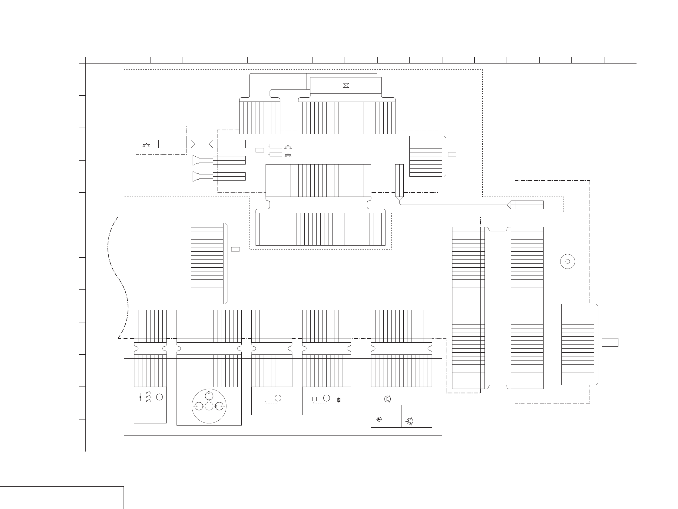
GV-D200/D200E/D800/D800E
FRAME SCHEMATIC DIAGRAM (2/2)
VCOM
VCOM
8 REG_GND
22PANEL_R
VCC_1
10
3
VCC_1
VBC
CLS
7 PANEL_B
23AD_6
REG_GND
11
264
REG_GND
STBYB
RES
6 PANEL_G
DEW
12
1
DEW
SRT
PSS1
5 PANEL_R
24REG_GND
25SP_L_+
924 7
OE
CLR
MCLK
HCNT
SPD
PSS2
CLD
CTR
1 SP_L_-
2 SP_L_+
3 REG_GND
4 AD_6
26SP_L_-
27NC
28NC
29NC
15P
CN4404
1
GV-D800/D800E MODEL
38
5 13
A
10P
B
LS-56 BOARD
2P
CN01
C
S001
(LCD ON/OFF)
D
SPEAKER L
SPEAKER R
SP901
SP902
1AD_6
2GND
PL-53
HARNESS
1 AD_6
2 GND
1 SP_L_+
2 SP_L_-
1 SP_R_+
2 SP_R_-
CN5604
1 LED_GND
2PCN5608
2PCN5506
2PCN5505
E
1
2
3
4
F
G
TO(1/2)
H
I
J
8P
CN4401
M-SW(C)
M-SW(B)
M-SW(A)
COM_GND
1234567
FP-220
FLEXIBLE
5
6
8
7
M-SW(A)
M-SW(C)
M-SW(B)
COM_GND
LM(+)
LM(+)
LM(-)
LM(-)
8
2
4
3
1
LM(-)
LM(-)
LM(+)
LM(+)
5
6
7
8
9
10
11
12
13
14
15
16
17
18
19
20
16P
CN3101
LP2Y2LP2X3GND4LP1X5LP1Y6GND7GND8GND9XODD10YODD11GND12XEVEN13YEVEN14GND15FEY16FEX
1
3
2
4
1
GND
LP1X
LP2X
LP2Y
M
K
S901
MODE
SWITCH
M903
LOADING
MOTOR
20PCN933
SWP
AFC_FO
BPF_MONI
F0_ADJ_RF_IN
PB_RF
REG_GND
RF_AGC_OUT
VC_RF_SWP
NC(EVF_BL)
NC(EVF_BL_4.6V)
NC(VCO)
NC(EVF_VG)
DV_RF_SWP
RF_IN
CAP_FG
RF_MON
TMS
TCK
TDO
TDI
8
6
9
7
5
GND
GND
GND
LP1Y
SP1Y
ODD EVEN
CPC
(FOR CHECK)
10
11
14
12
16
15
13
FEX
FEY
GND
GND
SP1X
SP2X
SP2Y
FE
VIDEO
HEAD
6
2 LED
3 BL_LOW
4 N.C
5 N.C
6 N.C
7 N.C
LCD
26P
CN5503
1SP_R_+
2SP_R_-
3REG_GND
32P
CN923
CN4402 10P
PG
FG-PG_COM
FG
COMWWVVUU
123456789
8
7
9
10
FG
PG
COM
FG-PG_COM
FG
PG
DRUM MOTOR
26 SP_R_+
M901
8 N.C
S5601
BLIGHT+
S5602
BLIGHT-
25 SP_R_-
4BL_CONT
6
W
9 N.C
10 BL_HIGH
20 REG_GND
21 PANEL_13.3V
22 PANEL_-15.3V
23 BL_CONT
24 REG_GND
5PANEL_-15.3V
6PANEL_13.3V
7REG_GND
8REG_GND
9PANEL_4.75V
VC-250 BOARD(2/2)
10
5
4
2
3
1
V
V
U
U
W
M
24P
CN5501
VSS
VGL
VDD
N.C.
VGH
GND
VDD3V
SPS
VGH
VGL
123456789
14 XCS_LCD_DA
15 XVC_SCK
16 REG_GND
17 PANEL_2.8V
18 PANEL_4.75V
19 REG_GND
FP-569
10PANEL_2.8V
11REG_GND
12XVC_SCK
13XCS_LCD_DA
14VC_SO
15REG_GND
12P
CN4403
FRC
STAND_BYVSMT_GND
FG_OUT
OFFSET_ADJ
123456789
9
12
10
11
FRC
FG_OUT
STAND_BY
OFFSET_ADJ
FG
CAPSTAN MOTOR
ND901 BACK LIGHT
LCD 901
4 INCH COLOR LCD UNIT
STBYB
RESET
GRES
GPCK
GSRT
MO1
EX2
MO2
EX1
MO3
101112131415161718192021222324
PD-130 BOARD
LCD DRIVER(1/2)
BACK LIGHT(2/2)
9 PANEL_HOLD
10 C-SYNC/XHD
11 PANEL_XVD
12 REG_GND
13 VC_SO
FLEXIBLE
16PANEL_XVD
17
18PANEL_-HOLD
19REG_GND
20PANEL_B
21PANEL_G
C-SYNC/XHD
MT_GND
VCC_2
VS
FP-433
FLEXIBLE
5
8
7
VS
VS
VCC_2
MT_GND
MT_GND
M
M902
DEW
SENSOR
10
VSS
VDD
VG
VG
30NC
TAPE_TOP(C)
14
TAPE_TOP(C)
VSH
VB
VSH3V
VB
GND
VSH5V
2P
CN5607
1 BL_LOW
31NC
32NC
HI8_MP
S_REEL(+)
ME/MP
REC_PROOF
S_REEL(-)
FP-221
FLEXIBLE
9
13
12
10
ME/MP
HI8_MP
S_REEL(-)
S_REEL(+)
REC_PROOF
VR
VR
REG_GND
123456789
15
REG_GND
FP-249
Q002
TAPE END
FP-355
FLEXIBLE
D001
TAPE LED
2 BL_HIGH
TAPE_END(C)
8
TAPE_END(C)
11 1514
10P
CN5502
C_LOCK_SW
TAPE_LED(K)
SENSOR_VCC
T_REEL(+)
T_REEL(-)
HALL_COM
TAPE_LED(A)
1011121314
6115
7
HALL_COM
TAPE_LED(A)
4
T_REEL(-)
3
T_REEL(+)
2
TAPE_LED(K)
SENSOR_VCC
15
1
C_LOCK_SW
1VB
2XVD_OUT
3VG
4PANEL_COM
5VR
6SHARP/XCASIO
7C-SYNC/XHD
8XHD_OUT
9GND
10GND
CPC
(FOR CHECK)
EP-51
CN931
12
HARNESS
40P
1VIDEO_GND
2V/Y_IN
3V/Y_IN_GND
4AUDIO_R_IN
5AUDIO_R_IN_GND
6AUDIO_L_IN
7AUDIO_L_IN_GND
8LANC_SIG
9LANC_GND
10ID1
11ID2
12VIDEO_GND
13VIDEO_OUT
14VIDEO_OUT_GND
15AUDIO_R_OUT
16AUDIO_R_OUT_GND
17AUDIO_L_OUT
18AUDIO_L_OUT_GND
19C_IN
20VIDEO_GND
21IO_GND
22IO_GND
23EX_UNREG
24EX_UNREG
25EX_UNREG
26EX_UNREG
27REG_GND
28REG_GND
29REG_GND
30REG_GND
31BL_GND
32BL_GND
33BL_GND
34BL_REG
35BL_REG
36BL_REG
37REG_GND
38REG_GND
39BEEP
40BEEP
FP-570
FLEXIBLE
H001,002
S/T REEL
SENSOR
FP-356
FLEXIBLE
Q001
TAPE TOP
FLEXIBLE
1
BL_HIGT
2
BL_LOW
1 VIDEO_GND
2 V/Y_IN
3 V/Y_IN_GND
4 AUDIO_R_IN
5 AUDIO_R_IN_GND
6 AUDIO_L_IN
7 AUDIO_L_IN_GND
8 LANC_SIG
9 LANC_GND
10 ID1
11 ID2
12 VIDEO_GND
13 VIDEO_OUT
14 VIDEO_OUT_GND
15 AUDIO_R_OUT
16 AUDIO_R_OUT_GND
17 AUDIO_L_OUT
18 AUDIO_L_OUT_GND
19 C_IN
20 VIDEO_GND
21 IO_GND
22 IO_GND
23 EX_UNREG
24 EX_UNREG
25 EX_UNREG
26 EX_UNREG
27 REG_GND
28 REG_GND
29 REG_GND
30 REG_GND
31 BL_GND
32 BL_GND
33 BL_GND
34 BL_REG
35 BL_REG
36 BL_REG
37 REG_GND
38 REG_GND
39 BEEP
40 BEEP
CN205
CN203
2P
40P
EX-36 BOARD
BZ201
BUZZER
CN204
20P
1VIDEO_OUT
2VIDEO_OUT_GND
3V/Y_IN
4VIDEO_IN_GND
5AUDIO_R_IN
6AUDIO_L_IN
7AUDIO_IN_GND
8LANC_SIG
9IO_GND
10LANC_GND
11ID1
12EX_GND
13EX_GND
14AUDIO_R_OUT
15AUDIO_L_OUT
16AUDIO_OUT_GND
17ID2
18EX_UNREG
19EX_UNREG
20C_IN
MULTI
CONNECTOR
1716
MECHANISM DECK(B710 MECHA)
L
16
FRAME SCHEMATIC DIAGRAM (2/2)
4-3 4-4

GV-D200/D200E/D800/D800E
4-2. PRINTED WIRING BOARDS AND SCHEMATIC DIAGRAMS
THIS NOTE IS COMMON FOR WIRING BOARDS AND SCHEMATIC DIAGRAMS
(In addition to this, the necessary note is printed in each block)
GV-D200/D200E/D800/D800E
(For printed wiring boards)
• b: Pattern from the side which enables seeing.
(The other layers' patterns are not indicated.)
• Through hole is omitted.
• Circled numbers refer to waveforms.
• There are few cases that the part printed on diagram
isn’t mounted in this model.
• Chip parts.
C
BE
5
64
2
13
Transistor
5
46
2
31
45
2
31
12
4
53
Diode
3
21321321
(For schematic diagrams)
• All capacitors are in µF unless otherwise noted. pF : µ
µF. 50V or less are not indicated except f or electrolytics
and tantalums.
• Chip resistors are 1/10W unless otherwise noted.
kΩ=1000Ω, MΩ=1000kΩ.
• Caution when replacing chip parts.
New parts must be attached after removal of chip.
Be careful not to heat the minus side of tantalum
capacitor, Because it is damaged by the heat.
• Some chip part will be indicated as follows.
Example C541 L452
22U 10UH
TA A 2520
(Measuring conditions voltage and waveform)
• Voltages and waveforms are measured between the
measurement points and ground when composite video
signal is REC or PB. They are reference values and
reference waveforms. *
(VOM of DC 10 MΩ input impedance is used.).
• V oltage v alues change depending upon input impedance
of VOM used.)
When indicating parts by reference number, pleas include
the board name.
Kinds of capacitor
Temperature characteristics
External dimensions (mm)
• Constants of resistors, capacitors, ICs and etc with XX
indicate that they are not used.
In such cases, the unused circuits may be indicated.
• Parts with ★ differ according to the model/destination.
Refer to the mount table for each function.
• All variable and adjustable resistors have characteristic
curve B, unless otherwise noted.
• Signal name
XEDIT→ EDIT PB/XREC → PB/REC
• 2: non flammable resistor
• 1: fusible resistor
• C : panel designation
• A : B+ Line *
• B : B– Line *
• J : IN/OUT direction of (+,–) B LINE. *
• C : adjustment for repair. *
• Circled numbers refer to waveforms. *
* Indicated by the color red.
Note :
The components identified by
mark 0 or dotted line with mark
0 are critical for safety.
Replace only with part number
specified.
Note :
Les composants identifiés par
une marque 0 sont critiques
pour la sécurité.
Ne les remplacer que par une
pièce portant le numéro spécifié.
4-5
 Loading...