

Page 1
DVP-S715
RMT-D102P
SERVICE MANUAL
SPECIFICATIONS
Russian Model
MICROFILM
CD/DVD PLAYER
Page 2

WARNING!!
WHEN SERVICING, DO NO T APPR O A CH THE LASER
EXIT WITH THE EYE TOO CLOSELY. IN CASE IT IS
NECESSARY TO CONFIRM LASER BEAM EMISSION,
BE SURE TO OBSERVE FROM A DISTANCE OF
MORE THAN 25 cm FROM THE SURFACE OF THE
OBJECTIVE LENS ON THE OPTICAL PICK-UP BLOCK.
CAUTION:
The use of optical instrument with this product will increase eye
hazard.
CAUTION
Use of controls or adjustments or performance of procedures
other than those specified herein may result in hazardous radiation exposure.
SAFETY CHECK-OUT
After correcting the original service problem, perform the following
safety checks before releasing the set to the customer:
1. Check the area of your repair for unsoldered or poorly-soldered connections. Check the entire board surface for solder
splashes and bridges.
2. Check the interboard wiring to ensure that no wires are
“pinched” or contact high-wattage resistors.
3. Look for unauthorized replacement parts, particularly transistors, that were installed during a previous repair. Point them
out to the customer and recommend their replacement.
SAFETY-RELATED COMPONENT WARNING!!
COMPONENTS IDENTIFIED BY MARK ! OR DOTTED
LINE WITH MARK ! ON THE SCHEMA TIC DIAGRAMS
AND IN THE PARTS LIST ARE CRITICAL TO SAFE
OPERATION. REPLACE THESE COMPONENTS WITH
SONY PARTS WHOSE PART NUMBERS APPEAR AS
SHOWN IN THIS MANUAL OR IN SUPPLEMENTS PUBLISHED BY SONY.
4. Look for parts which, though functioning, show obvious signs
of deterioration. Point them out to the customer and recommend their replacement.
5. Check the B+ voltage to see it is at the values specified.
– 2 –
Page 3

TABLE OF CONTENTS
Section Title Page Section Title Page
Service Note ............................................................................ 4
5. IC PIN FUNCTION DESCRIPTION
1. GENERAL
This Player Can Play the Following Discs .................... 1-1
Getting Started .............................................................. 1-1
Basic Operations ........................................................... 1-2
Playing Discs in Various Modes .................................... 1-4
Setting and Adjustments ............................................... 1-8
Additional Information ................................................... 1-9
2. DISASSEMBLY
2-1. Case Removal ............................................................... 2-1
2-2. Front Panel Section Removal........................................ 2-1
2-3. MB-78 Board Removal .................................................. 2-1
2-4. AU-205 Board Removal ................................................ 2-1
2-5. MD Block Ass’y Removal .............................................. 2-2
2-6. TK-47 Board Removal................................................... 2-2
2-7. Tray Removal ................................................................. 2-2
2-8. Skew Motor (M903) Removal ....................................... 2-2
2-9. Sled Motor (M501) Removal ......................................... 2-3
2-10. Spindle Motor (M901) Removal .................................... 2-3
2-11. Optical Pick-up Removal............................................... 2-3
2-12. Internal Views ................................................................ 2-4
2-13. Circuit Boards Location ................................................. 2-5
3. BLOCK DIAGRAMS
3-1. Overall Block Diagram .................................................. 3-1
3-2. RF/Servo Block Diagram .............................................. 3-3
3-3. Signal Process Block Diagram ..................................... 3-5
3-4. Video Block Diagram ..................................................... 3-7
3-5. System Control Block Diagram..................................... 3-9
3-6. Audio Block Diagram..................................................... 3-11
3-7. Mode Control Block Diagram ........................................ 3-13
3-8. Power Block Diagram.................................................... 3-15
4. PRINTED WIRING BOARDS AND SCHEMATIC
DIAGRAMS
4-1. Frame Schematic Diagram ........................................... 4-1
4-2. Printed Wiring Boards and Schematic Diagrams ......... 4-5
TK-47 Printed Wiring Board .......................................... 4-5
TK-47 Schematic Diagram ............................................ 4-7
MB-78, FG-43 Printed Wiring Boards........................... 4-12
MB-78 (AV Decoder) Schematic Diagram .................... 4-17
MB-78 (Video Encoder) Schematic Diagram................ 4-21
MB-78 (Drive), FG-43 (Sled) Schematic Diagrams...... 4-25
MB-78 (DSP) Schematic Diagram ................................ 4-28
MB-78 (Bias) Schematic Diagram ................................ 4-31
MB-78 (IF µ-com) Schematic Diagram ......................... 4-34
MB-78 (ARP, L Gate Array, Decrypt)
Schematic Diagram ....................................................... 4-37
MB-78 (System µ-com, S Gate Array)
Schematic Diagram ....................................................... 4-41
HP-96 Printed Wiring Board and
Schematic Diagram ....................................................... 4-45
AU-205 Printed Wiring Board ....................................... 4-49
AU-205 Schematic Diagram ......................................... 4-51
FL-88, FR-133 Schematic Diagrams ............................ 4-54
FL-88, FR-133 Printed Wiring Boards .......................... 4-57
ER-2 Schematic Diagram ............................................. 4-61
ER-2 Printed Wiring Board............................................ 4-65
PS-415 Printed Wiring Board and
Schematic Diagram ....................................................... 4-70
POWER BLOCK (HS-930SH)
Printed Wiring Board and Schematic Diagram............. 4-73
5-1. Interface Control Pin Function (MB-78 Board IC604) .. 5-1
5-2 System Control Pin Function (MB-78 Board IC805) .... 5-2
6. TEST MODE
6-1. Starting up Test Mode ................................................... 6-1
6-2. Selection of Check Item ................................................ 6-1
6-2-1. Selected Item Check ................................................ 6-1
6-2-2. All Items Check ........................................................ 6-1
6-3. Error Display.................................................................. 6-2
6-4. General Description of Checking Method..................... 6-2
6-5. Drive Auto Adjustment .................................................. 6-9
6-6. Drive Manual Operation ................................................ 6-13
6-6-1. Drive Manual Operation menu screen..................... 6-13
6-6-2. Disc T ype.................................................................. 6-13
6-6-3. Manual Control 1...................................................... 6-13
6-6-4. Manual Control 2...................................................... 6-14
6-6-5. Manual Control 3...................................................... 6-14
6-6-6. Manual Adjust 1 ....................................................... 6-14
6-6-7. Manual Adjust 2 ....................................................... 6-15
6-6-8. Auto Adjust ............................................................... 6-15
6-6-9. Check ....................................................................... 6-15
6-6-10. EEPROM data screen display ................................. 6-16
6-7. Other Operation............................................................. 6-16
6-8. Emergency History........................................................ 6-17
6-9. Error Code ..................................................................... 6-19
7. ELECTRICAL ADJUSTMENT
7-1. Power Supply Check ..................................................... 7-1
1. HS-930SH Board........................................................... 7-1
7-2. Adjustment of System Control ...................................... 7-2
1. System Clock 27 MHz Adjustment ................................ 7-2
7-3. Adjustment of Video System......................................... 7-2
1. Video Level Adjustment ................................................ 7-2
2. S-Terminal Output Check .............................................. 7-2
3. Checking Composite Video Output B-Y........................ 7-2
4. Checking Composite Video Output R-Y ....................... 7-3
5. Checking Composite Video Output Y............................ 7-3
6. Checking S Video Output S-C....................................... 7-3
7. Checking S Video Output DC Level .............................. 7-3
7-4. Adjustment Related Parts Arrangement ....................... 7-4
8. REPAIR PARTS LIST
8-1. Exploded Views ............................................................. 8-1
8-1-1. Case Assembly ........................................................ 8-1
8-1-2. Front Panel Assembly .............................................. 8-2
8-1-3. Chassis Assembly.................................................... 8-3
8-1-4. DVD Mechanism Chassis Assembly (1) .................. 8-4
8-1-5. DVD Mechanism Chassis Assembly (2) .................. 8-5
8-2. Electrical Parts List ....................................................... 8-6
– 3 –
Page 4
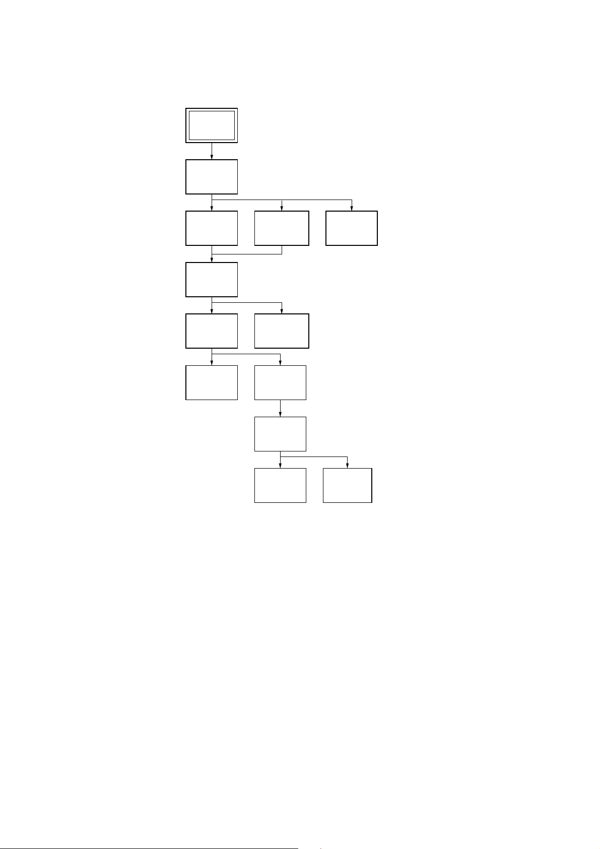
SERVICE NOTE
1. DISASSEMBLY
• This set can be disassembled in the order shown below.
Set
Case
(Page 2-1)
MB-78
Board
(Page 2-1)
MD Block
Ass’y
(Page 2-2)
Tray
(Page 2-2)
Optical
Pick-up
(Page 2-3)
Front Panel
Section
(Page 2-1)
TK-47
Board
(Page 2-2)
Skew
Motor
(Page 2-2)
Spindle
Base
(Page 2-3)
Spindle
Motor
(Page 2-3)
AU-205
Board
(Page 2-1)
Sled
Motor
(Page 2-3)
– 4 –
Page 5
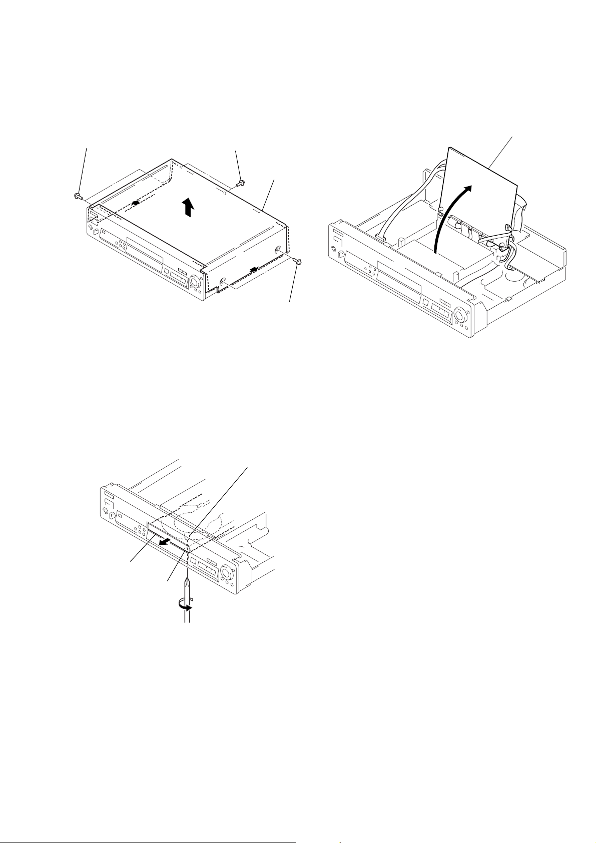
2. NOTE ON REMOVE THE CASE
MB-78 board
1) Remove six tapping screws. (See Fig. 1)
2) Open the side of case. (See Fig. 1)
3) Remove the case as lift straight. (See Fig. 1)
4. HOW TO SERVICE MB-78 BOARD
1) Remove the case from the set. (Refer to 2-1)
2) Remove the cover (upper). (Refer to 2-3)
3) Set the MB-78 board as shown in Fig. 3.
Note: Do not disconnect wiring.
Two tapping screws
Two tapping screws
Case
Two tapping screws
Fig. 1
3. DISK REMOVAL PROCEDURE
(at POWER OFF)
1) Insert a cross-tip screwdriver into a hole at the bottom, and
rotate the cam gear 1 in direction A. (See Fig. 2)
Note: To pr event a damege of cam gear, rotate it in direction
A by 1/4 turn.
2) Draw out the tray 2 in direction B by hand, and remove a
disk. (See Fig. 2)
Fig. 3
2 Tray
B
Hole
A
Fig. 2
1 Cam gear
– 5 –
Page 6
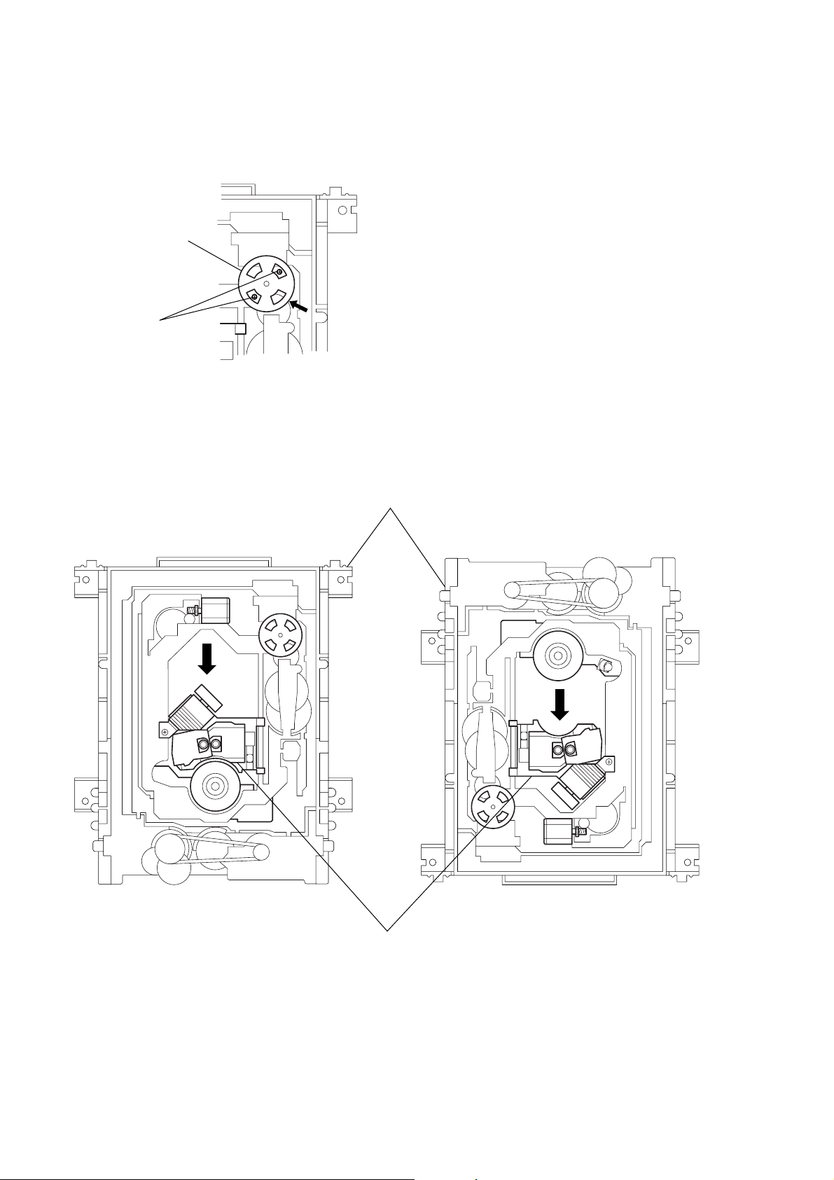
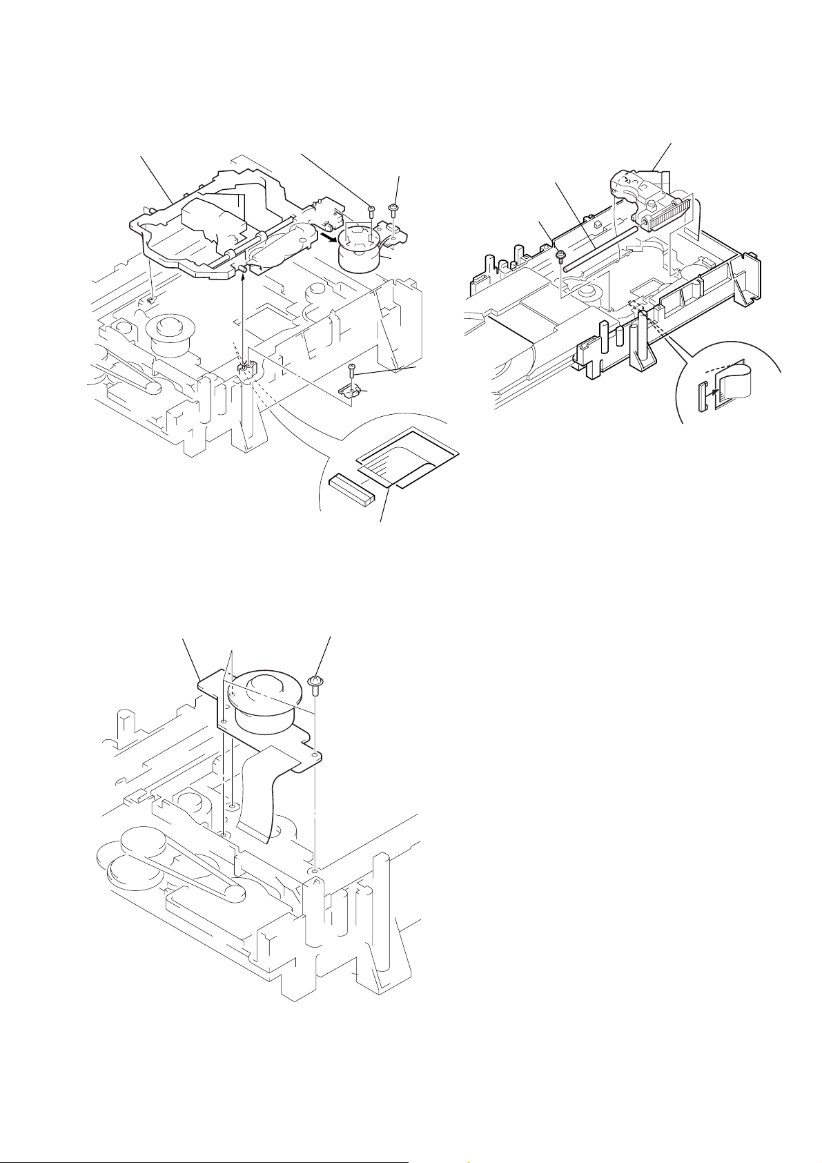
5. NOTE ON MOUNTEING SLED MOTOR
1) Push the sled motor ass’y 1 toward direction A. (See Fig. 4)
2) Tighten two screws 2 (M1.7 × 2.5).
1 Sled motor ass’y
A
2 Two screws (M1.7 × 2.5)
Fig. 4
3) Raising the MD block ass’y 3 90 º with the side down.
confirm that the optical pick-up 4 falls by self weight.
(See Fig. 5)
4) Further, with the front side of MD block ass’y 3 up, confirm
that the optical pick-up falls by self weight.
3 MD block ass’y
Upper
Lower Front side
4 Optical pick-up
Upper
Lower
Front side
Fig. 5
– 6 –
Page 7
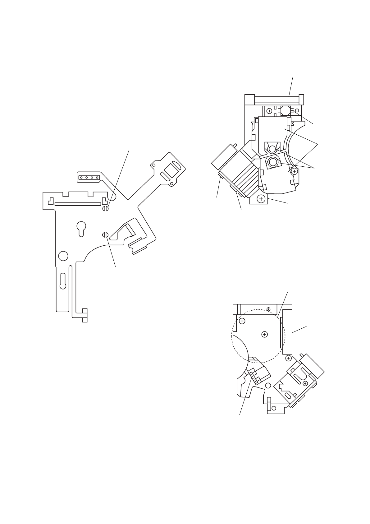
6. REPLACING OPTICAL PICK-UP
6-1. Handling
1) A red laser diode for DVD requires more attention to static
electricity than general infrared laser diodes for CD.
Because its durability to static electricity is far weaker than
that of infrared laser diodes, always use an earth band when
handling the optical pick-up block as service parts.
2) As for the flexible board KHS-180A (RP) packed as service
parts, the short lands have been soldered to protect from static
electricity. Accordingly, remove solders when replacing optical pick-up. (See Fig. 6)
DVD short land
3) In handling the KHS-180A (RP), do not touch inhibited parts
shown in Fig. 7, but grip the slide base bearing and U-shaped
guide.
Slide base bearing
Skew sensor
Lens actuator
covers
Objective lenses
CD short land
Fig. 6 Flexible board
Laser holder
U-shaped guide
OEIC
Touch inhibited parts
• Objective lens
• Skew sensor
• Laser holder
• Laser coupler
• Flexible board
• OEIC
• Lens actuator covers
Flexible board
Connector
– 7 –
Laser coupler
Fig. 7 KHS-180A (RP)
Page 8
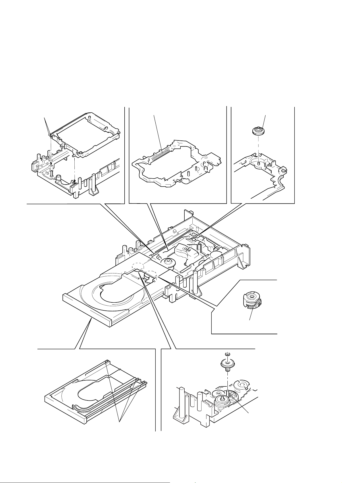
7. NOTE ON ASSEMBLING MECHANICAL DECK
7-1. Application of Grease
1) Grease must be applied if the following parts were replaced.
(See Fig. 8)
Note 1: Recommended grease is Foil KG-70MP.
Note 2: In applying grease, take care not to allow grease to
stick to other parts (particularly, rubber belt, spindle
motor, and optical pick-up)
Base unit holder
2 bosses
Slide base Skew cam
Tray 3 grooves
Note:Add grease if tray
moves slowly.
Cam gear
Loading pulley shaft
Note:Add grease if tray
generates noise
periodically.
Fig. 8
– 8 –
Page 9
7-2. Cleaning Spindle Motor Turntable
1) Remove the tray. (Ref er to 2-7)
2) Clean the spindle motor turntable if disc antiskid rubber (black)
is dirty. (See Fig. 9)
7-4. Deformation of Insulator
1) Assemble the spindle base into the base unit.
2) Lock with 4 shoulder screws. (See Fig. 11)
3) Check if 4 insulators deformed. (See Fig. 11)
Spindle motor
Turntable
Fig. 9
7-3. Aligning Phase of Cam Gear and
Drive Gear
1) Align triangle marks when assembling the cam gear and drive
gear. (See Fig. 10)
Four step screws
Two insulators
Insulator
Two insulators
Good NG
Fig. 11
7-5. Note on Mounting FG-43 Board
1) Align two bosses. (See Fig. 12)
2) Fix the board securely with screws (PTPWH2 × 5). (The sen-
sor will not function normally if the board floats up.)
Drive gear Cam gear
Align triangle marks.
Screw
(PTPWH2 × 5)
FG-43 board
Two bosses
Fig. 10
Fig. 12
– 9 –
Page 10
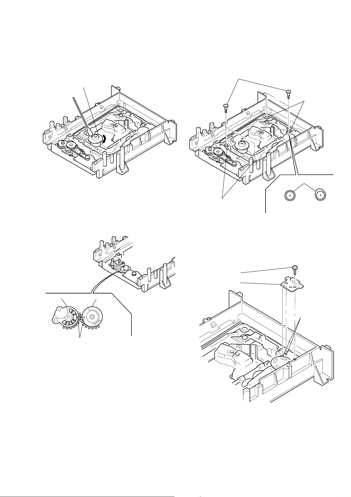
7-6. Note on Mounting TK-47 Board
1) Align two bosses. (See Fig. 13)
2) Align four tabs. (See Fig. 13)
3) Fix the board securely with 3 screws (BV3 × 10). (The sensor
will not function normally if the board floats up.)
Three screws
TK-47 board
Two claws
(BV3 × 10)
Boss
Two claws
Boss
Fig. 13
7-7. Note on connecting OPT Harness
1) The optical pick-up could be destroyed unless the OPT harness is connected normally to the connector. (See Fig. 14)
OPT harness
Good NG
Connector
Fig. 14
– 10 –
Page 11
SECTION 1
GENERAL
DVP-S715
This section is extracted from D VPS715/S315 instruction manual.
1-1
Page 12
1-2
Page 13
1-3
Page 14
1-4
Page 15
1-5
Page 16
1-6
Page 17
1-7
Page 18
1-8
Page 19
1-9
Page 20
1-101-10 E
Page 21
SECTION 2
7 Two flat cables
(CN201, 203)
4 Four screws
(BVTP3 × 10)
6 AU-205 board
3 Connector
(CN205)
5 Two screws
(B3)
1 Flat cable
(CN202)
2 Connector
(CN204)
DISASSEMBLY
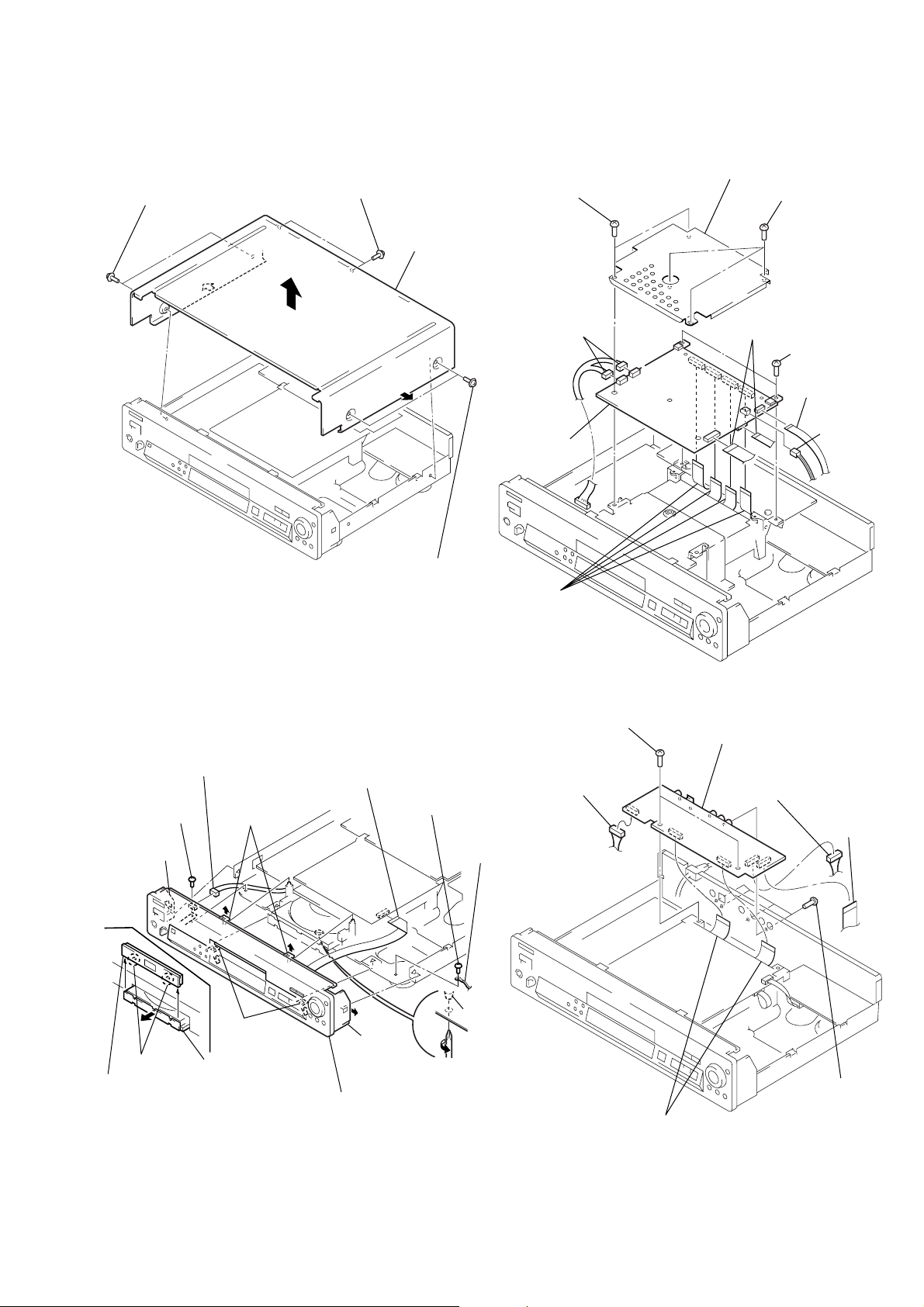
Note: Follow the disassembly procedure in the numerical order given.
2-1. CASE REMOVAL 2-3. MB-78 BOARD REMOVAL
7 Cover (upper)
1 Two tapping screws
2 Two tapping screws
4 Case
5 Two screws
(B3)
DVP-S715
6 Three screws
(B3)
3 Two tapping screws
2-2. FRONT PANEL SECTION REMOVAL
1 Two connectors
(CN001, 002)
9 MB-78
board
0 Four flat cables
(CN101, 252, 301, 452)
2-4. AU-205 BOARD REMOVAL
2 Two flat cables
(CN301, 601)
8 Two screws
(B3)
3 Flat cable
(CN251)
4 Connector
(CN361)
1 Connector
7 Screw
(B3)
0 Claw
5 Two claws
6 Tray ornamental
panel ass’y
(CN001)
!£ Two claws
!¡ Two claws
4 Draw out the
tray by hand.
2 Flat cable
(CN601)
!™ Claw
3 Rotate the cam gear
in direction A.
!¢ Front panel section
8 Screw
(B3)
9 Lug
Cam gear
A
2-1
Page 22
2-5. MD BLOCK ASS’Y REMOVAL 2-7. TRAY REMOVAL
3 Chassis
bracket (B)
5 Two screws
(B3)
6 Clamp
1 Cover (lower)
2 Two screws
(B3)
4 Two screws
(B3)
7 MD block
ass’y
1 Two screws
(BVTP3 × 10)
2 Press pully bracket
4 Pull the tray.
6 Remove the
tray.
A
5 Claw
3 Rotate the cam gear
in direction A.
2-6. TK-47 BOARD REMOVAL 2-8. SKEW MOTOR (M903) REMOVAL
1 Screw
(PT WH2 × 5)
3 Skew gear retainer
4 Skew motor
(M903)
2 Flat cable
(spindle
motor)
(CN002)
1 Connector
(CN004)
4 Four screws
(BVTP3 × 10)
6 TK-47 board
3 OP-15
flexible
board
(CN001)
5 Two claws
2 Claw
2-2
Page 23
2-9. SLED MOTOR (M501) REMOVAL 2-11. OPTICAL PICK-UP REMOVAL
4 Spindle base
6 Two screws
(P1.7 × 2.5)
5 Screw
(PTTWH2 × 5)
7 Sled motor
3 Skew shaft
stopper
1 OP-15 flexible
board
(CN001)
4 Optical pick-up
3 Main shaft
2 Screw
(PTTWH2 × 5)
(M501)
2 Screw
(P2 × 8)
1 OP-15 flexible board
(CN001)
2-10. SPINDLE MOTOR (M901) REMOVAL
2 Spindle motor
(M901)
1 Three screws
(PTTWH2 × 5)
2-3
Page 24
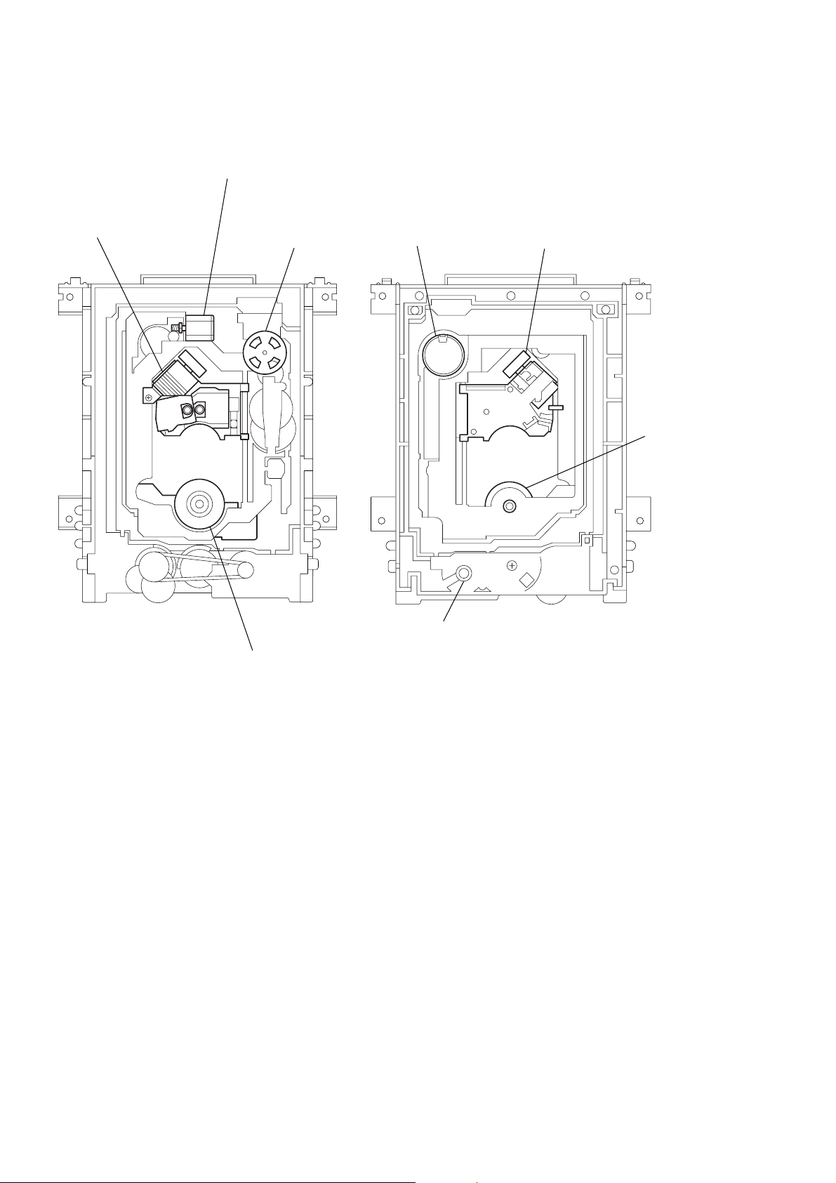
2-12. INTERNAL VIEWS
Skew motor ass’y (tilt)
X-3947-138-1
Optical pick-up
(KHS-180A/J1N)
8-820-005-02
Sled motor ass’y
X-3947-137-1
Sled motor ass’y
X-3947-137-1
Optical pick-up
(KHS-180A/J1N)
8-820-005-02
DC motor
(spindle)
1-698-944-11
DC motor (spindle)
1-698-944-11
Motor (loading)
1-698-942-21
2-4
Page 25
2-13. CIRCUIT BOARDS LOCATION
POWER BLOCK
(HS-930SH)
(SWITCHING REGULATOR)
MB-78
(SIGNAL PROCESS/SERVO)
HP-96
(HEAD PHONE)
FR-133
(IR/POWER SWITCH)
DC MOTOR
(SPINDLE)
FL-88
(FL DRIVER/FUNCTION SWITCH)
TK-47
(RF/SERVO)
ER-2
(EURO AV)
AU-205
(AUDIO)
FG-43
(SLED)
PS-415
(AUDIO POWER)
2-5
2-5 E
Page 26
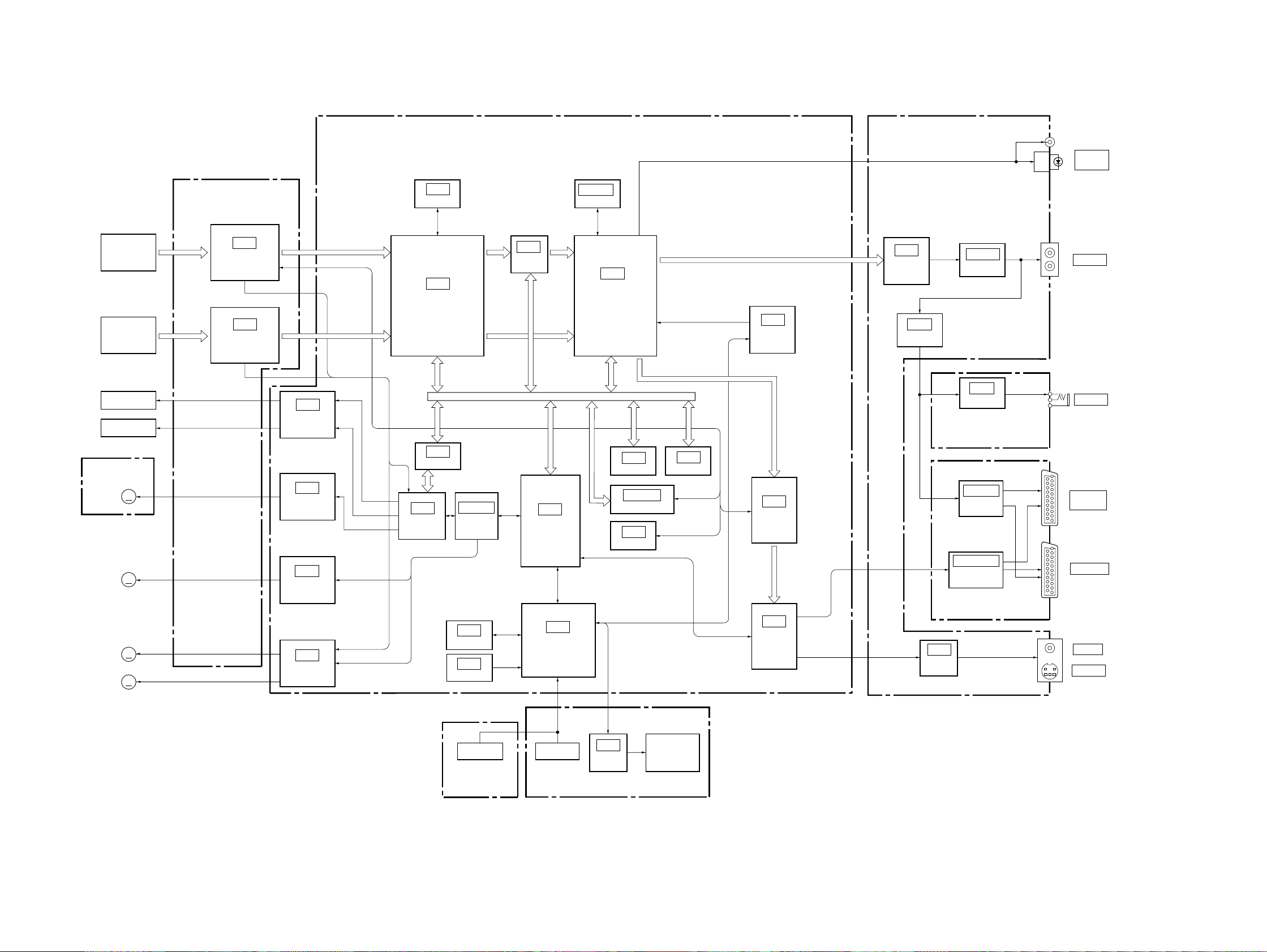
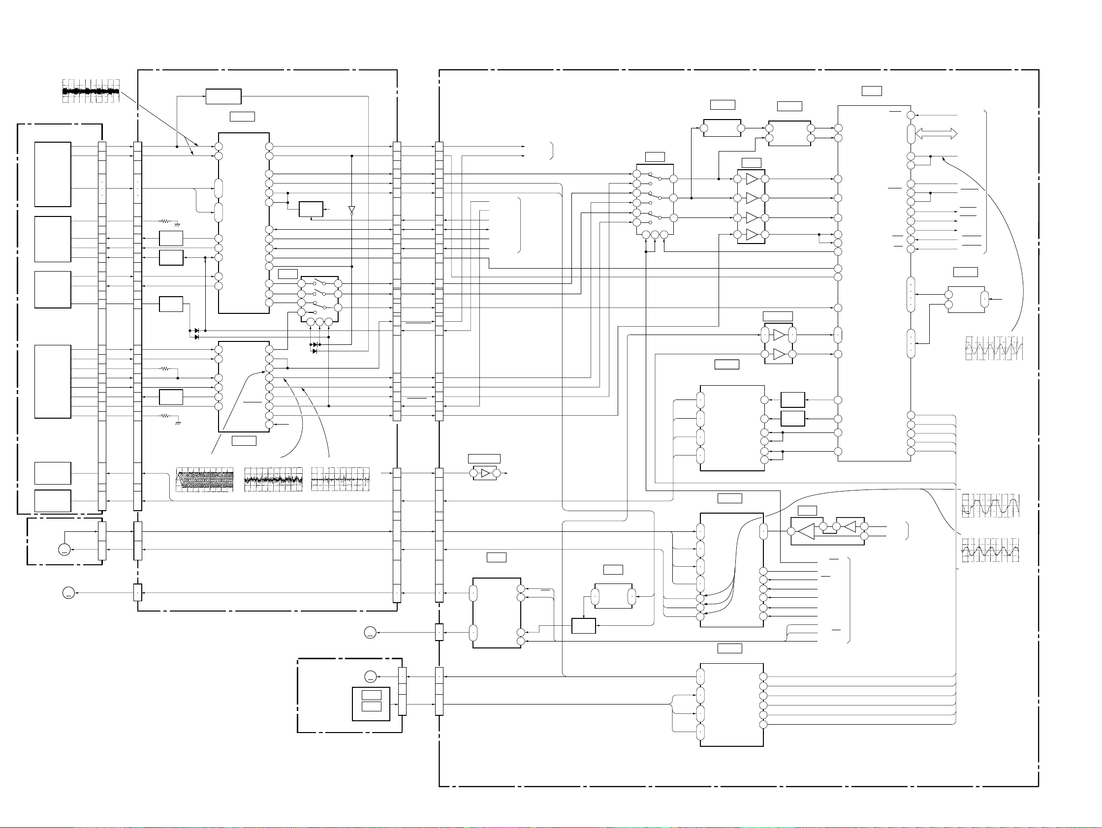
3-1. OVERALL BLOCK DIAGRAM
DVP-S715
SECTION 3
BLOCK DIAGRAMS
DVD OPT
CD OPT
FOCUS COIL
TRACKING COIL
FG-43 BOARD
(SEE PAGE 4-27)
M503
M
SLED
MOTOR
M901
MOTOR
M902
MOTOR
M903
TILT
MOTOR
M
M
M
SPINDLE
LOADING
TK-47 BOARD
(SEE PAGE 4-7)
DVD RF AMP,
IC006
SERVO
IC005
CD RF AMP,
SERVO
IC363
FOCUS/TRACKING
COIL DRIVE
IC302
SLED MOTOR
DRIVE
IC303
SPINDLE MOTOR
DRIVE
IC361
TILT/LOADING
MOTOR DRIVE
MB-78 BOARD
(SEE PAGE 4-17~4-44)
DVD RF
CD RF
IC810
4M DRAM
IC806
IC807
S GATE ARRAY
IC506
SERVO DSP
ARP
HA0-21, HD0-15
IC804 (1/2)
LGATE
ARRAY
IC603
ROM
IC605
RESET
SD0-7
CD_BCK,
CD_LRCK,
CD_DATA,
SPDIF
IC811
DECRYPT
SYSTEM µ-COM
DCRSD
IC851
IC604
IF µ-COM
AU-205 BOARD
(SEE PAGE 4-51)
SPDIF
IC201, 202
16M SRAM
0-7
IC203
AV DECODER
IC802
1M SRAM
IC804 (2/2)
L GATE ARRAY
IC801
EEPROM
AV_DATA, AV_BLK, AV_LRCK
YC0-7
IC803
8M ROM
IC207
OSD
IC251
DNR
IC252
VIDEO
ENCODER
Y0-7
C0-7
IC204
AUDIO 2CH
DAC
IC208
BUFFER
HP-96 BOARD
(SEE PAGE 4-45)
IC601-603, 607
ER-2 BOARD
(SEE PAGE 4-61)
IC209
VIDEO
BUFFER
IC206, 207
MIX AMP
BUFFER
IC001
HP AMP
IC604, 608
BUFFER
SW, BUFFER
DIGITAL
OUT
AUDIO
PHONE
EURO AV1
(RGB)-TV
EURO AV2
VIDEO
S VIDEO
SWITCH
FR-133 BOARD
(SEE PAGE 4-56)
05
SWITCH
FL-88 BOARD
(SEE PAGE 4-54)
IC101
FL DRIVER
ND101
FLUORESCENT
INDICATOR TUBE
3-1 3-2
Page 27
DVP-S715
3-2. RF/SERVO BLOCK DIAGRAM
OPTICAL DEVICE
DVD PD IC
DVD LD
MODULE
SKEW
SENSOR
CD LASER
COUPLER
CD FOCUS
TRACKING
COIL
DVD FOCUS
TRACKING
COIL
M901
SPINDLE
MOTOR
M902
LOADING
MOTOR
IC006 ^£ – ^¢ (DVD play)
800 mVp-p (V)
RFP
9
RFN
10
6
A-D
13
14
18
VR
5
DVD LD
3
PD
4
VLD
2
SKEW IN
41
SKEW OUT
42
LED
38
PD1
28
PD2
29
AL
19
CD_E
27
CD_F
20
CD_LD
23
MON
26
VR
25
CD FCS,
30
CD TRK
ı
33
DVD FCS,
DVD TRK
34
ı
37
U IN,
V IN,
W IN,
1
SPVH
ı
8
M
M
9
ı
11
LDMT
U OUT,
V OUT,
W OUT
TK-47 BOARD
(SEE PAGE 4-7)
CN001
9
10
6
13
14
18
5
3
4
2
41
42
38
28
29
19
27
20
23
26
25
30
ı
33
34
ı
37
CN002
1
ı
8
9
ı
11
CN004
1
2
Q004
SWITCH
Q005
SWITCH
Q001
LD ON
Q007
SWITCH
IC005 @™ (CD play)
500 mV/DIV 1 µs/DIV
Q009, IC004
RF DET
IC006
DVD RF AMP, SERVO
63
RFP
64
RFN
10
A
ı
ı
7
D
1
A2
ı
ı
4
D2
18
LD
17
PD
16
XLDON
20
TI-A
21
TI-B
3
PD1
4
PD2
5
E
6
F
1
LD
2
PD
IC005
CD RF AMP, SERVO
SIGO
57
HOLD1
47
37
PI
26
TIE
TII
23
TI–
24
43
SDATA
44
SCLK
ADEN
45
TIOFS
19
33
FDCHG
MIRR
MIRR
RF02
RF01
APC_ON
TE_C
IC005 !£ (CD play)
500 mV/DIV 1 ms/DIV
RFO
IC011
TE
FE
30
19
21
22
13
TE
15
FE
32
25
12
VC
16
Q008
SWITCH
SWITCH
338
139
13
12
10
9 11
VC
IC005 !∞ (CD play)
500 mV/DIV 10 ms/DIV
FG-43 BOARD
(SEE PAGE 4-27)
05
VC
4
15
14
M903
TILT MOTOR
M501
SLED MOTOR
CN005
Q009
CN008
VC
M
M
IC501
IC502
HALL SENSOR
CN501
26
9
23
10
11
3
19
18
17
4
20
22
27
16
21
13
14
15
12
2
1
16
ı
23
3
ı
10
11
ı
13
14
15
DVD_RF+
DVD_PI
DVD_FE
DVD LDON
CDRFDC
CD LDON
DVDFCS,
DVDTRK
TIMT
1
2
3
ı
8
DFCTS
TI-ERR
TIE
TTLT/H
SSSD
SCKG3
SDEN
TIOFS
DPD
MIRR
CDRF
CD TE
CD FE
TEATT
SVC
CDFCS,
CDTRK
U IN,
V IN,
W IN,
SPVH
U OUT,
V OUT,
W OUT
LDMT
SLDMT
HA, HB,
SLVH
MB-78 BOARD (1/6)
(SEE PAGE 4-25~4-30)
CN452
2
19
5
18
17
25
9
10
11
24
8
6
1
12
7
15
14
13
16
26
CN302
27
12
ı
5
25
ı
18
17
ı
15
13
14
1
2
7
8
1
ı
6
CN361
CN301
8
9
5
6
IC502 (1/2)
3 1
IC361
TILT/LOADING
MOTOR DRIVE
DOUT2
DOUT1
DVD LDON
CD LDON
TILT/H
SSSD
SCKG3
SDEN
MUTE2
IN2–
IN1+
MUTE1
DVD RF
CD RF
SYSTEM
CONTROL
(SEE PAGE 3-9)
VC
TRAY_FREE
13
OPN/CLS
17
21
S12VOFF
2
TI_ERR
TIE
SIGNAL PROCESS
(SEE PAGE 3-5)
Q452
SWITCH
IC506
89
TRIN
7
DFCTA
21
AIN5
AIN2
24
26
AIN0
GIO3
11
GIO2
12
8
GIO8
73
PWM2
99
TRREF
88
19
AIN6, 7
20
AIN8
18
2
GIO11
1
GIO12
49
AOUT0
AOUT1
46
SERVO DSP
HCK/HLDB
HDO-7
CLKIN
GIO10
MRST
GIO15
GIO13
HFD/HWR
HR/HRD
AOUT3
AOUT2
PWM1
PWM0
5
SYSTEM CONTROL
(SEE PAGE 3-9, 10)
TCK
IRS
GIO9
VTOP
VBTM
GIO0
MDS0
MDP0
72
56
ı
63
65
79
3
84
94
98
4
100
71
70
28
37
42
45
50
36
43
44
51
38
41
74
14
75
SIGNAL
PROCESS
(SEE PAGE 3-5)
HYCNTR
SDCNT
SOUT
SLOFS
TKC
HYCNTR
HYDET
SDCNT
SOUT
SLOFS
TKC
HYDET
IA1
IDO-7
27M_DSP
ACK
SDPRST
ERROR
BUSY2
IC507
POWER SUPPLY
7
OUT2
OUT1
1
SYSTEM CONTROL
(SEE PAGE 3-9, 10)
FON
SDSPWR
SDSPRD
3
IN
5
IC506 ^∞
3.6 Vp-p 27 MHz
IC303 !ª, @™, @£ (DVD play)
5.2 Vp-p 160Hz
IC303 !ª, @™, @£ (CD play)
1.84 Vp-p 45Hz
VC
IC508
FILTER
2 1 6 7
IN OUT
IC452
13
12
1
2
3
5
IC455
COMP
1
OUT
7
TIE
3
IN
5
TI_ERR
109 11
14
15
4
CD TRK
CDFCS
DVDFCS
DVDTRK
FOCUS/TRACKING
COIL DRIVER
11
DO2
12
13
DO1 MUTE2
14
15
DO4
16
17
DO3
18
SPINDLE MOTOR DRIVE
30
U IN
31
32
V IN
33
34
W IN
1
28
VH
29
23
U OUT
22
V OUT
19
W OUT
SLED MOTOR DRIVE
2
SLDMT
5
33
HA
34
29
HB
30
22
SLVH
23
IC363
IC363
IC303
IC302
IC503
3 1
6 7
10 8
12 14
MUTE1
IN2–
IN3–
IN1–
IN4–
Z1, Z2
HFG
NS+
SPCTRL1
SPCTRL0
SPGC2
SPGC1
DV–
DVI
DVO
TKC
CTRL
A+
IC501
COMP
IN2 OUT2
3 1
IN1 OUT1
IC502 (2/2)
5
10
12 14
Q371
9
MUTE
Q372
20
MUTE
6
23
3
26
14
15
27
7
8
9
10
11
8
12
13
18
25
32
PISW
7
8
IC301
–
671 2
+
CD/DVD
HFG
NST
SPCTRL1
SPCTRL0
SPGC2
SPGC1
TRAY_FREE
OPN/CLS
S12VOFF
3-3 3-4
Page 28
3-3. SIGNAL PROCESS BLOCK DIAGRAM
MB-78 BOARD (2/6)
(SEE PAGE 4-17, 4-37)
IC806 0
1.5 Vp-p
RF IN1DVD RF
10
RF IN2CD RF
RF/SERVO
(SEE PAGE 3-3, 4)
12
MDS0MDS0
43
MDP0MDP0
48
MA0-9
IC810
4M DRAM
MD00-15
IC806
ARP
XMWR, XCAS,
XRAS, XOE
SYSTEM CONTROL
(SEE PAGE 3-9, 10)
96
ı
99
SD0-7
101
ı
106
SDCK, XSHD,
106
XSRO, XSAK, SDEF
ı
109
IC207
OSD
SCLK
SO
SCLKO
CGCSO
OH SYNC
1
SD0-7 DCRSD0-7
3
74
77
DTI0-7
ı
79
80
4
ı
8
43-47 26-31 34-41
24
SIN
25
CS
26
EVEN
11
H SYVC
12
V SYNC
13
IC811
DECRYPT
XRST
54 51
SHA0-5
SHD0-7
R OUT
G OUT
B OUT
I OUT
DTO0-7
MCK
20
19
18
17
62
64
ı
66
68
ı
74
56
59
ı
61
AREQ, ALALID,
ERROR, TOS
VS
69
HS
70
88
ı
EX_OSD_0-3
91
12
ı
CH-DATA0-7
19
21
24
26
30
DCK
28
16M SDRAM
AVA0-11
AVID
IC201
0-15
SDQM, WE, CAS, RAS, CS1, CS2, SDQM, SDCLK
IC203
AV DECODER
IC202
16M SDRAM
PD0-7
DVP-S715
73
74
76
ı
78
82
ı
84
FID
V SYNC
YC0-7
VIDEO
(SEE PAGE 3-7)
MUTE
MD2
DFCT
NORF
LOCK
FWON
ARPINT
ARPCS
ARPWT
SYSTEM CONTROL
(SEE PAGE 3-9, 10)
05
XWR
XRD
DCRCS
DCRINT
DCRWT
AVDRQ
AVCS
AVINT
AVWT
XRST
MRST
IA0-8
ID0-7
MUTE
110
MD2
112
DFCT
50
NORF
51
LOCK
53
FWON
55
XINT
80
XCS
81
83
XWAT
IC806 `⁄¤¤
3.4 Vp-p 27 MHz
XRST
84 122
XWR, XRD
XRST
MCKI
SCKI
124
33M
27M_DSP
70-73 75-7856 57
IA0-7
IC806 `⁄¤›
3.0 Vp-p 33 MHz
A0-7
D0-7
56-62 64-67
ID0-7
CD_LRCK, CD_BCK,
CD_DATA, SPDIF
106
ı
109
XRST
XWR, XRD,
DCRCS, DCRINT, DCRWT
IA0-5
ID0-7
27M_DNR
IC811 %¡
3.4 Vp-p 27 MHz
98
99
101
102
58 59 63-65 68 94-96 100 34-39 43-45 47-54
XWR, XRD,
AVDRQ, AVCS,
AVINT, AVWT
KESET_B
57
MRST
384FS
IA0-8
A_0-8
SPDIF_OUT
BCLK
LRCLK
ASDATA
D_0-7
ID0-7
111
105
106
107
SPDIF
AV_BCK
AV_LRCK
AV_DATA
384FS
27M_DNR
27M_DSP
33M
AUDIO
(SEE PAGE 3-11)
SYSTEM CONTROL
(SEE PAGE 3-10)
3-5 3-6
Page 29

DVP-S715
3-4. VIDEO BLOCK DIAGRAM
MB-78 BOARD (3/6)
(SEE PAGE 4-21)
SIGNAL
PROCESS
(SEE PAGE 3-6)
SYSTEM
CONTROL
(SEE PAGE 3-9, 10)
MODE
CONTROL
(SEE PAGE 3-13)
05
YC0-7
FID
V SYNC
OHSYNC
27M_DNR
DCS
SCKG3
SOG3
H SYNC
V SYNC
27M_VE
MRST
13.5M
VCS
AVCK
SOG2
VSI
E_V/RGB
AVCNT
VS
E V/Y
V SYNC
V MUTE
OHSYNC
27M_DNR
DCS
SCKG3
SOG3
11
ı
GI 0-7
18
98 H SYNCI
9 BIO (27MHz)
29 XCS
30 XSCLK
31 SDI
IC251
DNR
XRST
DCLKI (13.5MHz)
93 100 97
MRST
13.5M
V SYNCI
G00-07
R00-07
IC252 &¢
0.7 Vp-p (H)
IC252 &™
0.7 Vp-p (H)
IC252 ^§
0.7 Vp-p (H)
IC252 %§
1.1 Vp-p (H)
IC252
VIDEO ENCODER
19
60
ı
67
51
ı
58
ı
22
PD0-7
24
ı
27
33
ı
36
PD8-15
38
ı
41
FID
14
V SYNC
15
16
H SYNC
PDCLK
XCS/SA
SCK/SCL
SYSCLK
MRST
27M_VE
XRST
13.5M
SI/SDASOVREF
4847 55454411108
VCS
AVCK
SOG2
VSI
ER-2 BOARD (1/2)
(SEE PAGE 4-61)
B-Y/R OUT
Y/G OUT
R-Y/B OUT
RV251
VIDEO
LEVEL
ADJ
CN251
CPOUT
YOUT
COUT
56
64
58
74
72
66
AVCNT
E_V/RGB
328649
E_V/RGB
AV CONT
782461
E V/Y
VIDEO B
EURO V/Y
VIDEO R
VIDEO G
IC252 ^¢
1.0 Vp-p (H)
CN603
Q601, 621, 624
AV CONT
CN252 (1/2)
VS
AV CONT L
AV CONT H
IC252 %•
0.7 Vp-p (H)
AU-205 BOARD (1/2)
(SEE PAGE 4-51)
CN201 (1/2)
VIDEO V
VIDEO Y
VIDEO C
V MUTE
VS
Q641
12
16
14
18
19
14 15 5 3 1
VS
V MUTE
VIDEO C
2 1 11 13 15
SWITCH
IC602
SWITCH
1
3
Q630
Q627
VIDEO V
VIDEO Y
IC601
Q632
SWITCH
INVERTER
CN202 (1/2)
CN602 (1/2)
1 3
2
2
AV CONT H
AV CONT L
Q215
7 4
7
14
10
12
8
7
2 15
4
7
1
5
AUDIO
(SEE PAGE 3-11)
IC209 !∞
IC209
VIDEO BUFFER
IC603
VIDEO BUFFER
2 15
4 13
7 10
1
MUTE
IC607
VIDEO BUFFER
4 13
7 10
1
MUTE
1.1 Vp-p (H)
13
10
Q214
VS
RY601
RY602
7
6
7
6
IC209 !£
1.0 Vp-p (H)
Y
C
8
5 1
Q628
RELAY DRIVE
58
1
Q629
RELAY DRIVE
VIDEO
S VIDEO
10
3
10
3
IC209 !º
J202 (1/2)
LINE OUT
0.7 Vp-p (H)
Q602, 636
SWITCH
20
19
15
11
7
16
8
20
19
15
11
7
16
V/Y IN
V/Y OUT
R/C
CNJ602 (1/2)
G
B
I
AV CONT OUT
V/Y IN
V/Y OUT
R/C
G
CNJ601 (1/2)
B
I
EURO AV1
(RGB)-TV
EURO AV2
Q639
BUFFER
Q638
3-7 3-8
Q635, 637
SWITCH
8
AV CONT IN
Page 30
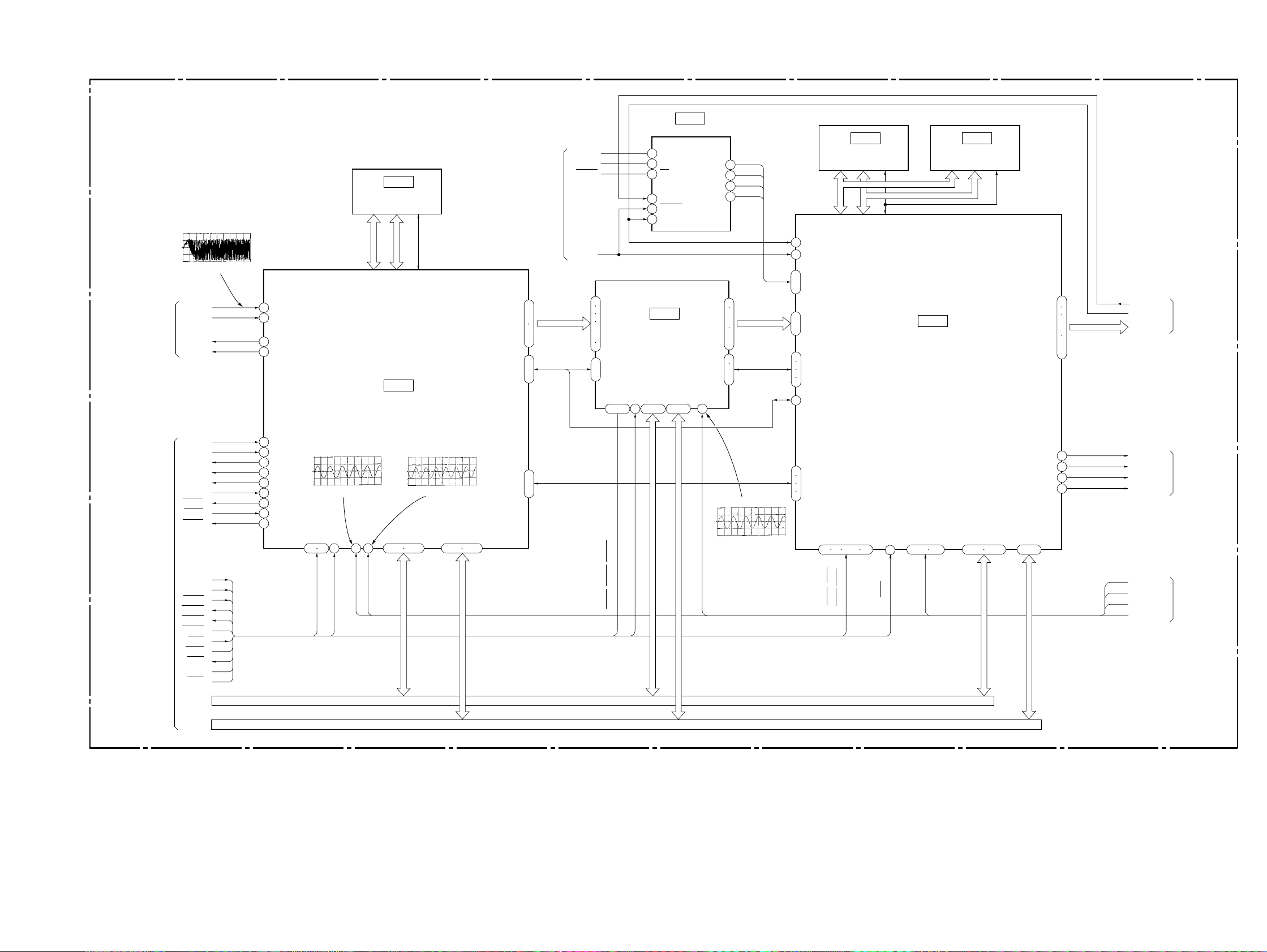
3-5. SYSTEM CONTROL BLOCK DIAGRAM
DVP-S715
MB-78 BOARD (4/6)
(SEE PAGE 4-17, 4-37, 4-41)
AUDIO
(SEE PAGE 3-11)
RF/SERVO
(SEE PAGE 3-3, 4)
POWER
(SEE PAGE 3-16)
SIGNAL
PROCESS
(SEE PAGE 3-5)
MODE
CONTROL
(SEE PAGE 3-13)
SCKG3
SOG3
D2LT
DVDLDON
CDLDON
TILT/H
SSSD
SCKG3
SDEN
CD/DVD
NST
SPCTRL1
SPCTRL0
SPGC2
SPGC1
S12VOFF
TRAY_FREE
OPN/CLS
ERROR
BUSY2
FON
SDSPWR
SDSPRD
S12VOFF
MUTE
MD2
DFCT
NORF
LOCK
FWON
ARPINT
ARPCS
ARPWT
XRD
XWR
DCRCS
DCRINT
DCRWT
AVCS
AVWT
OHSYNC
XIFBSY
IFSI
IFSO
DIAG
XSHINT
IC801
EEPROM
SOG3
SCKG3
MLT
OHSYNC
EBSY, ECS,
EESI, EWC
46
47
117
50
2
3
13
52
48
4
7
8
9
10
22
19
18
5
15
14
17
77
58
104
103
105
106
16
102
60
59
61
56
57
62
63
64
65
66
140
132
44
109
125
133
SCKG3
SOG3
D2LT
MLT
DVDLDON
CDLDON
TILT/H
SSSD
SDEN
CD/DVD
NST
SPCTRL1
SPCTRL0
SPGC2
SPGC1
S12VOFF
TRAY_FREE
OPN/CLS
ERROR
BUSY2
FON
SDSPWR
SDSPRD
MUTE
MD2
DFCT
NORF
LOCK
FWON
ARPINT
ARPCS
ARPWT
IRD
IWR
DCRCS
DCRINT
DCRWT
AVCS
AVWT
OHSYNC
XIFBSY
IFSI
IFSO
DIAGN
XSHINT
IC804
L GATE ARRAY
HA0-7, 19-21
HD0-7
MRST
27M_VE
SCKG2
DOUTCTL
DCS
AVCNT
E_V/Y
E_V/RGB
HSYNC
PDCLK
VCS
AVCK
IC807
1
ı
3
5
ı
8
ı
CGCS
SCLK
SI
SCKG1
SRST
HA0-8
HD0-7
CSI
SCKI
SDI
S GATE ARRAY
MODE
CONTROL
(SEE PAGE 3-13)
IC206 8
3.28 Vp-p 27 MHz
44
ı
50
IA0-8 IA1
52
53
33
ı
36
ID0-7
38
ı
41
57
SCO
56
SCKO
SDO
55
61
CK
384FS
33M
27M_DNR
27M_DSP
384FS_2CH
27M_DSP
IC204
716 2
SIGNAL
PROCESS
(SEE PAGE 3-6)
AUDIO
(SEE PAGE 3-11)
RF/SERVO
(SEE PAGE 3-4)
27M_DNR
27M_VE
ID0-7
IA0-8
ID0-7
CGCSO
SCLKO
SO
RF/SERVO
(SEE PAGE 3-4)
SIGNAL
PROCESS
(SEE PAGE 3-5)
VIDEO
(SEE PAGE 3-7)
IC802
1M SRAM
75
HA0-7, 19-21
76
83
ı
91
HD0-7
92
ı
99
HA0-21
23-30 32-39 41 42 44-47 4-11 13 14 16-21
RD, WR, CS0, CS1
RD, WR
73
74
XIRQ3, XIRQ7,
67
XCS6, XWAIT
68
71
72
SIG1, 2
69
70
108
123
115
113
158
49
149
150
151
127
118
36
114
37
VSI
152
VS
SOG1
48
49
57
59
2
55
56
69
107
109
108
54
MRST
SCK1
TXD1
PA11
112 110
65
PA0/CS4
53 64
A0-11
SYSTEM µ-COM
IC805 &£
PA10
IC804 `⁄⁄fi
3.3 Vp-p 27 MHz
IC805
4.4 Vp-p 20 MHz
A MUTE
MA MUTE
DOUTCTL
OHSYNC
SCKG3
SOG3
DCS
AVCNT
E_V/Y
E_V/RGB
HSYNC
13.5M
VCS
AVCK
SOG2
VSI
VS
IC803
8M FLASH
HD0-15
AD0-15
AIDIO
(SEE PAGE 3-11)
VIDEO
(SEE PAGE 3-7)
PB0
PB14/IRQ9
PA9
IRQ2
IRQ1
IRQ0
PB1
EXTAL
XTAL
SCK0
RES
HA0-8
HD0-7
97
1
63
68
67
66
98
73
74
111
79
MLT
SCKG3
SOG3
X201
27MHz
SYSCLK
(27MHz)
20MHz
CT201
ADJ
IC804 `⁄⁄°
X801
24
HFG
RF/SERVO
ACK
(SEE PAGE 3-4)
SDPRST
VIDEO
VSYNC
(SEE PAGE 3-7)
AVDRQ
SIGNAL
PROCESS
AVINT
(SEE PAGE 3-5)
XRST
SIGNAL PROCESS,
MRST
VIDEO, AUDIO
(SEE PAGE 3-5, 7, 11)
IC209
PLL
RSTB 384FS
ML
7
8
MC
9
MD
XT1
1
XT2
IC209 1
1.4 Vp-p 27 MHz
33M
27M
2010
21
63
64
11
14
16
19
23
24
25
IC205
BUFFER
5 6
2 3
12 11
IC206
BUFFER
24 3
5 6
12 11
9 8
225 mVp-p 13.5 MHz
05
3-9 3-10
Page 31

DVP-S715
3-6. AUDIO BLOCK DIAGRAM
MODE CONTROL
(SEE PAGE 3-13)
SYSTEM CONTROL
(SEE PAGE 3-9)
SIGNAL PROCESS
(SEE PAGE 3-6)
SYSTEM CONTROL
(SEE PAGE 3-9,10)
MB-78 BOARD (5/6)
(SEE PAGE 4-21)
05
PMUTE
AUDIO MUTE
MA MUTE
AMUTE
SCKG3
D2LT
SOG3
SPDIF
AV_LRCK
AV_BCK
AV_DATA
DOUTCTL
384FS-2CH
MRST
CN252 (2/2)
IC208
CN101
20
17
19
18
16
5
4
5
3
1
8
MAMUTE
AUDIO MUTE
SCKG3
D2LT
SOG3
SPDIF OUT
DAC LRCK
DAC BCK
DAC DATA
384FS-2CH
MRST
AU-205 BOARD (2/2)
(SEE PAGE 4-51)
CN201 (2/2)
6
9
7
8
10
21
CN203
22
21
23
IC201
1
25
18
7
5
3
62
HP_L
HP_R
COAXIAL
OPTICAL
L
R
2
4
6
J201
J202 (2/2)
LINE OUT AUDIO
RV001
LEVEL
CN001
HP-96 BOARD
(SEE PAGE 4-45)
DIGITAL
OUT
IC011
HP AMP
5 7
3 1
Q001, 002
MUTE
J001
PHONE
Q209
MUTE DRIVE
IC207
IC206
BUFFER
BUFFER
Q203
MUTE
Q204
MUTE
2 16 7
6 72 1
1
3
2
ı
5
LRCIN
BCLK IN
D IN
XTI
RSTB
PFAIL
IC204
AUDIO 2CH DAC
V_OUT L
V_OUT R
ZERO
16
21
13
IC203
D-FF
3
D1
6
D3
4
D2
9
CLK
15
Q6
10
Q4
12
Q5
POWER
(SEE PAGE 3-15)
26
28
22
IC211
6
2
3
5
Q211
MUTE
Q210
MUTE DRIVE
Q212
MUTE
Q205
MUTE
7
T201
IC208
HEAD PHONE AMP
3 1
5 7
IC210
1
DIN
CN205
5
3
PMUTE
1
1
ER-2 BOARD (2/2)
(SEE PAGE 4-61)
VIDEO
(SEE PAGE 3-8)
AV CONT L
AV CONT H
CN202 (2/2)
CN602 (2/2)
MUTE_CTL
Q606, 640, 612
MUTE CTL
11 913
AU_R (X)
AU_L (X)
573
Q622, 623
MUTE
Q604, 605
MUTE
IC608
BUFFER
3 1
5 7
Q625, 626
MUTE
IC604
BUFFER
3 1
5 7
Q633, 634
MUTE
Q614, 615
MUTE
3
A (L) OUT
1
A (R) OUT
6
A (L) IN
2
A (R) IN
3
A (L) OUT
1
A (R) OUT
6
A (L) IN
CNJ602 (2/2)
EURO AV1
(RGB)-TV
CNJ601 (2/2)
EURO AV2
Q607, 608
MUTE
3-11 3-12
2
A (R) IN
Page 32

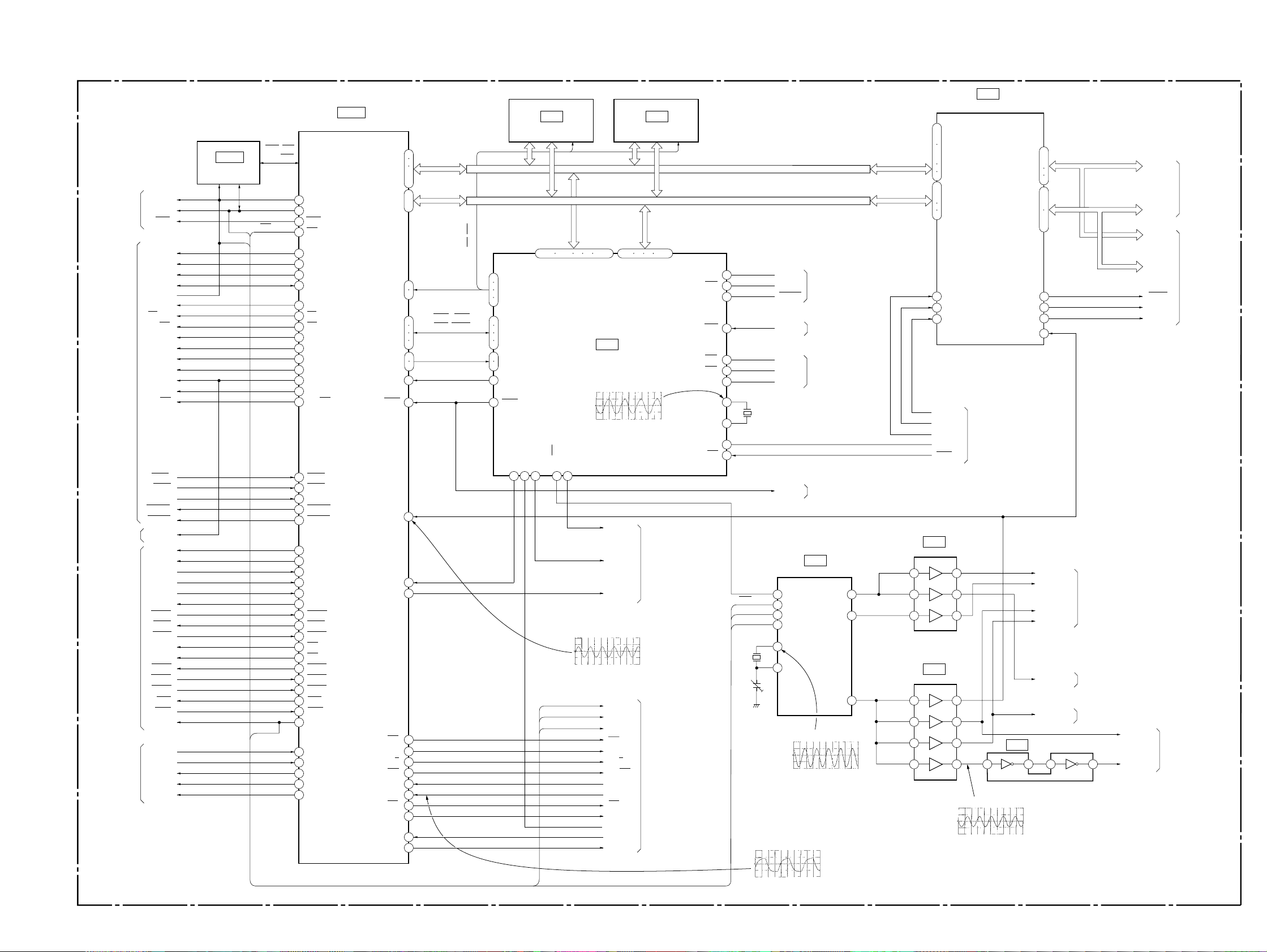
3-7. MODE CONTROL BLOCK DIAGRAM
MB-78 BOARD (6/6)
(SEE PAGE 4-34)
VIDEO
SEE PAGE
3-7
POWER
SEE PAGE
3-16
AUDIO
SEE PAGE
3-11
SYSTEM
CONTROL
SEE PAGE
3-9, 10
VSYNC
VMUTE
P_CONT
IC605
RESET
3OUT
PMUTE
AUDIO MUTE
XIFBSY
SCKGI
IFSI
IFSO
CGCS
SI
SCLK
DIAG
SRST
IC604
I/F µ-COM
53
REFV
25
VIDEO MUTE
33
P CONT
77
RESET IN
26
AUDIO MUTE
16
INTMS
20
SCK
19
TX
18
RX
28
CGCS
22
SO
24
SCLK
32
PPG6
54 IFCSXSHINT
IC606
COMP.
ST-BY CONT 1 OUT1 IN1
A00–019 AD00–07
SCLK
FLCS
RESET
AD6
AD4
AD3
CCW
CW
X IN
X OUT
55
IR
59
SO
22
24
30
31
45
43
41
58
57
83
82
X601
4MHz
IC604 *™
5.6 Vp-p 4 MHz
DVP-S715
FL-88 BOARD
(SEE PAGE 4-54)
3
CN601 CN101
IR
8
10
11
12
17
SI
SCKL
FLCS
AD5/6
8
10
11
12
17
S106
SUBTITLE
ON/OFF
IC 101
FL DRIVER
6
SI
8
SCLK
FLCS
9
S105
SUBTITLE
CHANGE
44
ı
G1–7 G1–7
38
15
ı
32
S1–19
•
35
50
JOG
S107
ANGLE
CHANGE
S108
AUDIO
CHANGE
S109
DNR
ND101
FLUORESCENT
INDICATOR TUBE
5
ı
11
43
S1–19
ı
25
D121
JOG
CN102 CN401
IR
2
FR-133 BOARD
(SEE PAGE 4-56)
2
EVER
5V
REG5V
1
Q401
LED
DRIVER
IC401
REMOTE
CONTROL
RECEIVER
D401
ON/STANDBY
ALE, OE, WE
IC601
LATCH
05
IC603
ROM
POWER SW
CN103
4
UP, DOWN
4
RIGHT, LEFT,
•
6
ı
9
1
2
AD4
16
15
6
5
AD3
CCW
CW
16
S123
OPEN/
CLOSE
15
S115
STOP
6
5
S122
PLAY
S114
PAUSE
S116
PREV
S117
NEXT
S118
JOG
S121
TITLE
S120
DVD
MENU
S119
RETURN
ENTER
CCW
CW
4
S401
POWER
JOG/CURSOL
BUTTON
3-13 3-14
Page 33

DVP-S715
3-8. POWER BLOCK DIAGRAM
AC IN
HS-930SH BOARD
(SEE PAGE 4-74)
CN101
F101
1
•
2
CN902
1
•
2
CN901
1
•
3
CN903
1
•
2
CN951
1
•
4
L101, 102
PS-415 BOARD
(SEE PAGE 4-71)
F901
D951-954
D955
MB-78 BOARD
(SEE PAGE 4-17~4-44)
DP+5V
FL008
A+5V
FL005
IC601
IC603
9
EVER 5V
7
7
•
8
3
5
1
7
2
5
4
CN002
CN201
F006
F005
FL002
FL006
11
17
22
P_CONT
EVER 5V
A+5V
D+5V
FL001
FL007
FL003
EVER+5.3V
MODE CONTROL
(SEE PAGE 3-13)
CN252
15
9
4
AU+5V
S+5V
D+5V
EVER+5V
D+3.3V
PC101
PHOTO
COUPLER
T101
E–12V
IC202
+5V REG
P311
P312
P211
Q312
POWER
CONTROL
P511
Q512
-12V SWITCH
E12V
CN601
1
3
ER-2 BOARD
(SEE PAGE 4-61)
IC201 IC203
IC204
IC604
IC608
D101
1
CN204
Q101–103
SWITCH
1
4
5
Q206-208
SWITCH
AU+12V
AU–12V
P.FAIL
CN202
Q202
+9V REG
31
LFT
LF901
LFT
IC951
+12V REG
IC953
–12V REG
Q951, 952
SWITCH
AU+12V
Q311
5.2V REG
IC611
3.3V REG
Q211
12V REG
Q511
-12V REG
HP-96 BOARD
(SEE PAGE 4-45)
IC011
CN001
51
AU–9V
AU+9V
26
CN205
CN201 CN001
1
REG+5.2V
•
2
EVER+5.3V
6
REG+3.3V
4
P-CONT
8
AU+12V
9
M+12V
14
AU-12V
11
–12V
12
IC602
IC607
CN602
8
A+5V
8
CN202
IC209
IC210
IC211
IC301 IC452 IC455
IC501 IC502 IC503
IC506 IC507 IC508
CN601
CN302 CN008
3
•
4
IC802
IC801 IC803
IC804 IC805
IC807 IC811
Q001, 002
SWITCH
S12V OFF
IC812
LPF
IC201 IC202 IC203
IC208 IC810
IC251
IC252
IC204 IC205 IC206
IC207 IC209
IC601 IC602 IC603
IC604 IC605 IC606
1
EVER+5V
CN101
20
S+5V
IC806
FL-88 BOARD
(SEE PAGE 4-54)
TK-47 BOARD
(SEE PAGE 4-7)
24
•
25
F004
F003
F002
F001
SYSTEM CONTROL
(SEE PAGE 3-9)
IC302
IC303
IC361
IC363
IC004 IC005
IC006 IC011
CN001
CN102 CN401
VCC
22
EVER 5V
1
1
OPTICAL
DEVICE
FR-133 BOARD
(SEE PAGE 4-56)
IC401
AU–12V
P.FAIL
05
4
5
AU-205 BOARD
(SEE PAGE 4-51)
P.FAIL
Q201
–9V REG
AUDIO
(SEE PAGE 3-11)
IC206 IC207
IC208
AU+5V
1
25
2
4
D+5V
REG-10V
3-15 3-16 E
19
IC101
Q101,102
+F, -F
17
DC-DC
CONVERTER
ND101
REG 5V
5
5
Q401
Page 34

SECTION 4
PRINTED WIRING BOARDS
AND
SCHEMATIC DIAGRAMS
THIS NOTE IS COMMON FOR PRINTED WIRING
BOARDS AND SCHEMATIC DIAGRAMS.
(In addition to this, the necessary mote is printed
in each block.)
For printed wiring boards:
• X : indicates a lead wire mounted on the component
side.
• x : indicates a lead wire mounted on the printed side.
• ® : Through hole.
• p : Parts mounted on the conductor side.
• b : Pattern from the side which enables seeing.
• b : Pattern on the rear side.*
• Circled numbers refer to waveforms.
Caution:
Pattern face side: Parts on the pattern face side seen from
(Conductor Side) the pattern face are indicated.
Parts face side: Parts on the parts face side seen from
(Component Side) the parts face are indicated.
4-1. FRAME SCHEMATIC DIAGRAM
DVP-S715
For schematic Diagram:
• Caution when replacing chip parts.
New parts must be attached after removal of chip.
Be careful not to heat the minus side of tantalum capacitor,
because it is damaged by the heat.
• All resistors are in ohms, 1/
less otherwise specified.
kΩ : 1000Ω, MΩ : 1000kΩ.
• All capacitors are in µF unless otherwise noted. pF : µµF
50V or less are not indicated except for electrolytics and
tantalums.
• All variable and adjustable resistors hav e characteristic curve
B, unless otherwise noted.
• 2 : nonflammable resistor.
• 1 : fusible resistor.
• C : panel designation.
• ¢ : internal component.
• C : adjustment for repair.*
• A : B+ Line.*
• B : B– Line.*
• J : IN/OUT direction of B line (+, –).*
• Circled numbers refer to waveforms.*
• V oltages are dc between measurement point.*
• Readings are taken with a color-bar signals on DVD refer-
ence disc and when plying CD reference disc.*
• Readings are taken with a digital multimeter (DC 10MΩ).*
• Voltage variations may be noted due to normal production
tolerances.*
Note:The components identified by mark ! or dotted line
with mark ! are critical for safety.
Replace only with part number specified.
4
W (Chip resistors : 1/
10
W) un-
When indicating parts by reference
number, please include the board
name.
• * : indicated by the color red.
FRAME
4-1 4-2 4-3
Page 35

DVP-S715
4-2. PRINTED WIRING BOARDS AND SCHEMA TIC DIAGRAMS
TK-47 (RF , SERVO) PRINTED WIRING BOARD
– Ref. No.: TK-47 board; 3,000 series –
POWER BLOCK
(HS-930SH)
(SWITCHING REGULATOR)
HP-96
(HEAD PHONE)
FR-133
(IR/POWER SWITCH)
FG-43
(SLED)
AU-205
(AUDIO)
PS-415
(AUDIO POWER)
TK-47 BOARD
CN001 D-3
CN002 H-2
CN004 G-1
CN005 B-4
CN008 B-3
D003 C-4
D004 E-2
IC004 C-4
IC005 D-4
IC006 F-3
IC011 E-5
Q001 E-2
Q004 E-2
Q005 E-2
Q007 D-4
Q008 F-3
Q009 F-3
Q010 D-3
DC MOTOR
(SPINDLE)
FL-88
(FL DRIVER/FUNCTION SWITCH)
ER-2
(EURO AV)
MB-78
(SIGNAL PROCESS/SERVO)
TK-47
(RF/SERVO)
4-5
Page 36

There are few cases that the part isn't mounted in this model is printed on this diagram.
TK-47
A
B
C
D
BOARD
E
F
G
1-669-298-
H
05
1
2
3 4
5 6
11
(11)
4-6
Page 37

• Wavef orms
TK-47 (RF, SERVO) SCHEMATIC DIAGRAM
– Ref. No.: TK-47 board; 3,000 series –
DVP-S715
DVP-S715
1 IC006 %¡ – %™ (DVD play)
270 mVp-p (V)
2 IC006 ^¡ – ^™ (DVD play)
1.2 Vp-p (V)
3 IC006 ^£ – ^¢ (DVD play)
4 IC005 !£ (CD play)
500 mV/DIV 1 ms/DIV
5 IC005 !∞ (CD play)
500 mV/DIV 10 ms/DIV
6 IC005 @™ (CD play)
800 mVp-p (V)
500 mV/DIV 1 µs/DIV
4-7 4-8 4-9 4-10 4-11
Note:The components identified by mark ! or dotted line
with mark ! are critical for safety.
Replace only with part number specified.
RF/SERVO
TK-47
Page 38

DVP-S715
A
MB-78
BOARD(SIDE A)
B
C
D
E
F
G
H
I
1
2
3
4
5
6
7
8
9
10
11
13
05
1-669-30-
1-669-300-
A
MB-78
BOARD(SIDE B)
B
C
D
E
F
G
H
I
1
2
3
4
5
6
7
8
9
10
11
13
05
1-669-300-
MB-78 (SIGNAL PROCESS), FG-43 (SLED) PRINTED WIRING BOARDS
– Ref. No.: MB-78 board; 1,000 series, FG-43 board; 3,000 series –
There are few cases that the part isn't mounted in this model is printed on this diagram.
FG-43
BOARD
MB-78 BOARD (SIDE A)
CN001 H-1
CN002 G-1
CN251 B-11
CN303 A-7
CN361 C-11
CN451 B-4
CN501 E-7
CN601 H-11
CN801 I-8
CN802 H-7
D102 A-4
D801 I-10
IC203 E-2
IC205 E-9
IC206 E-9
IC251 C-2
IC252 B-3
IC301 B-8
IC303 B-9
IC455 D-5
IC501 B-7
IC506 E-6
IC508 B-7
IC603 I-9
IC604 G-10
IC803 I-6
IC804 G-8
IC805 G-5
IC806 B-5
Q371 E-5
Q372 D-5
Q501 B-7
MB-78 BOARD (SIDE B)
CN101 A-3
CN252 A-9
CN301 C-1
CN302 A-5
CN452 A-7
D002 G-11
D101 A-9
D103 A-9
D502 E-5
D802 I-5
IC201 D-11
IC202 E-11
IC204 B-9
IC207 B-11
IC208 D-10
IC209 E-3
IC302 C-3
IC361 D-3
IC363 D-7
IC452 B-6
IC502 C-5
IC503 B-5
IC507 D-5
IC601 I-3
IC602 I-4
IC605 G-2
IC606 H-1
IC801 H-5
IC802 I-6
IC807 I-8
IC810 B-7
IC811 F-10
IC812 B-8
Q001 G-11
Q002 G-11
Q452 C-8
POWER BLOCK
FR-133
(IR/POWER SWITCH)
HP-96
(HEAD PHONE)
DC MOTOR
(SPINDLE)
(FL DRIVER/FUNCTION SWITCH)
(HS-930SH)
(SWITCHING REGULATOR)
FL-88
SIGNAL PROCESS, SLED
MB-78, FG-43
FG-43
(SLED)
AU-205
(AUDIO)
PS-415
(AUDIO POWER)
ER-2
(EURO AV)
(SIGNAL PROCESS/SERVO)
(RF/SERVO)
MB-78
TK-47
4-12
4-13 4-14
4-15 4-16
Page 39

MB-78 (AV DECODER) SCHEMATIC DIAGRAM
– Ref. No.: MB-78 board; 1,000 series –
DVP-S715
• Wavef orms
1 IC206 8
3.28 Vp-p 27 MHz
2 IC209 1
L64021-A-QC-27
1.4 Vp-p 27 MHz
4-17 4-18 4-19
4-20
AV DECODER
MB-78 (1/8)
Page 40

DVP-S715
• Wavef orms
MB-78 (VIDEO ENCODER) SCHEMATIC DIAGRAM • See page 4-12 to 4-16 for printed wiring board.
– Ref. No.: MB-78 board; 1,000 series –
1 IC252 &¢
2 IC252 &™
3 IC252 ^§
0.7 Vp-p (H)
0.7 Vp-p (H)
5 IC252 %•
0.7 Vp-p (H)
6 IC252 %§
1.1 Vp-p (H)
4 IC252 ^¢
0.7 Vp-p (H)
1.0 Vp-p (H)
VIDEO ENCODER
MB-78 (2/8)
4-21 4-22 4-23 4-24
Page 41

MB-78 (DRIVE), FG-43 (SLED) SCHEMATIC DIAGRAM • See page 4-12 to 4-16 for printed wiring board.
– Ref. No.: MB-78 board; 1,000 series, FG-43 board; 3,000 series –
DVP-S715
• Wavef orms
1 IC303 !ª, @™, @£ (DVD play)
5.2 Vp-p 160 Hz
2 IC303 !ª, @™, @£ (CD play)
1.84 Vp-p 45 Hz
4-25 4-26 4-27
Note:The components identified by mark ! or dotted line
with mark ! are critical for safety.
Replace only with part number specified.
DRIVE, SLED
MB-78 (3/8), FG-43
Page 42

DVP-S715
MB-78 (DSP) SCHEMATIC DIAGRAM • See page 4-12 to 4-16 for printed wiring board.
– Ref. No.: MB-78 board; 1,000 series –
• Wavef orm
1 IC506 ^∞
3.6 Vp-p 27 MHz
DSP
MB-78 (4/8)
4-28 4-29 4-30
Page 43

MB-78 (BIAS) SCHEMATIC DIAGRAM • See page 4-12 to 4-16 for printed wiring board.
– Ref. No.: MB-78 board; 1,000 series –
DVP-S715
DVP-S715
4-31 4-32
Note:The components identified by mark ! or dotted line
with mark ! are critical for safety.
Replace only with part number specified.
BIAS
MB-78 (5/8)
Page 44

DVP-S715
MB-78 (IF µ-COM) SCHEMATIC DIAGRAM • See page 4-12 to 4-16 for printed wiring board.
– Ref. No.: MB-78 board; 1,000 series –
• Wavef orm
1 IC604 *™
5.6 Vp-p 4 MHz
IF µ-COM
MB-78 (6/8)
4-34 4-35 4-36
Page 45

MB-78 (ARP, L GATE ARRAY, DECRYPT) SCHEMATIC DIAGRAM • See page 4-12 to 4-16 for printed wiring board.
– Ref. No.: MB-78 board; 1,000 series –
DVP-S715
• Wavef orms
1 IC804 `⁄⁄°
225 mVp-p 13.5 MHz
2 IC804 `⁄⁄fi
3.3 Vp-p 27 MHz
3 IC806 0
4 IC806 `⁄¤›
3.0 Vp-p 33 MHz
5 IC806 `⁄¤¤
3.4 Vp-p 27 MHz
6 IC811 %¡
1.5 Vp-p
4-37 4-38 4-39 4-40
3.4 Vp-p 27 MHz
ARP, L GATE ARRAY, DECRYPT
MB-78 (7/8)
Page 46

DVP-S715
• Waveform
MB-78 (SYSTEM µ-COM, S GATE ARRAY) SCHEMATIC DIAGRAM • See page 4-12 to 4-16 for printed wiring board.
– Ref. No.: MB-78 board; 1,000 series –
1 IC805 &£
4.4 Vp-p 20 MHz
SYSTEM µ-COM, S GATE ARRAY
MB-78 (8/8)
4-41 4-42 4-43 4-44
Page 47

HP-96 (HEAD PHONE) PRINTED WIRING BOARD AND SCHEMATIC DIAGRAM
– Ref. No.: HP-96 board; 4,000 series –
DVP-S715
There are few cases that the part isn't mounted in this model is printed on this diagram.
HP-96
BOARD(SIDE A)
HP-96
BOARD(SIDE B)
HP-96
(HEAD PHONE)
FR-133
(IR/POWER SWITCH)
DC MOTOR
(SPINDLE)
POWER BLOCK
(HS-930SH)
(SWITCHING REGULATOR)
FG-43
(SLED)
12
(12)
12
(12)
LEVEL
MIN MAX
PHONES
AU-205
(AUDIO)
PS-415
(AUDIO POWER)
ER-2
(EURO AV)
MB-78
(SIGNAL PROCESS/SERVO)
(FL DRIVER/FUNCTION SWITCH)
FL-88
4-45 4-46 4-47
TK-47
(RF/SERVO)
HEAD PHONE
HP-96
Page 48

• Wavef orms
1 IC209 !∞
DVP-S715
AU-205 (AUDIO) SCHEMATIC DIAGRAM
– Ref. No.: AU-205 board; 2,000 series –
2 IC209 !£
3 IC209 0
1.1Vp-p (H)
1.0 Vp-p (H)
0.7 Vp-p (H)
4-51 4-52 4-53
AUDIO
AU-205
Page 49

DVP-S715
FL-88 (FL DRIVER, FUNCTION SWITCH), FR-133 (IR, POWER SWITCH) SCHEMATIC DIAGRAMS
– Ref. No.: FL-88 board; 2,000 series, FR-133 board; 2,000 series –
FL DRIVER/FUNCTION SW, IR/POWER SW
FL-88, FR-133
4-54 4-55 4-56
Page 50

DVP-S715
FR-133
BOARD
12
(12)
ON/STANDBY
POWER
FL-88 (FL DRIVER, FUNCTION SWITCH), FR-133 (IR, POWER SWITCH) PRINTED WIRING BOARDS
– Ref. No.: FL-88 board; 2,000 series, FR-133 board; 2,000 series –
FL-88
BOARD(SIDE A)
A
B
C
05
1
2 3 4 5
6 7 8
1-669-302-
9 10 11 12 13
12
(12)
FL-88 BOARD (SIDE A)
CN101 C-4
CN103 C-1
D122 B-5
There are few cases that the part isn't mounted in this model is printed on this diagram.
A
B
C
05
FL-88
BOARD(SIDE B)
JOG
JOG
RETURN
1
DVD MENU
NEXT
TITLE
PREV
2 3 4 5
OPEN/CLOSE
6 7 8
REPEAT
CLEAR
SHUFFLE
PROGRAM
DNR
1-669-302-
9 10 11 12 13
12
(12)
FL-88 BOARD (SIDE B)
CN102 A-13
D121 A-1
D123 A-4
D125 A-4
D130 A-4
IC101 B-5
Q115 A-5
Q117 A-4
HP-96
(HEAD PHONE)
FR-133
(IR/POWER SWITCH)
DC MOTOR
(SPINDLE)
(FL DRIVER/FUNCTION SWITCH)
POWER BLOCK
(HS-930SH)
(SWITCHING REGULATOR)
FL-88
FG-43
(SLED)
AU-205
(AUDIO)
PS-415
(AUDIO POWER)
ER-2
(EURO AV)
MB-78
(SIGNAL PROCESS/SERVO)
TK-47
(RF/SERVO)
4-57 4-58 4-59 4-60
FL DRIVER/FUNCTION SW, IR/POWER SW
FL-88, FR-133
Page 51

DVP-S715
ER-2 (EURO AV) SCHEMATIC DIAGRAM
– Ref. No.: ER-2 board; 2,000 series –
EURO AV
ER-2
4-61 4-62 4-63 4-64
Page 52

ER-2 (EURO AV) PRINTED WIRING BOARD
POWER BLOCK
(HS-930SH)
(SWITCHING REGULATOR)
MB-78
(SIGNAL PROCESS/SERVO)
HP-96
(HEAD PHONE)
FR-133
(IR/POWER SWITCH)
DC MOTOR
(SPINDLE)
FL-88
(FL DRIVER/FUNCTION SWITCH)
TK-47
(RF/SERVO)
ER-2
(EURO AV)
AU-205
(AUDIO)
FG-43
(SLED)
PS-415
(AUDIO POWER)
– Ref. No.: ER-2 board; 2,000 series –
DVP-S715
There are few cases that the part isn't mounted in this model is printed on this diagram.
ER-2 BOARD (SIDE A)
D601 C-4
D607 A-5
D608 A-5
D609 A-6
D610 A-6
D616 A-2
D617 A-3
D618 A-3
D619 A-3
D620 A-4
D622 A-1
D623 A-2
D625 C-4
D626 C-2
D627 C-5
D628 B-2
IC603 B-2
IC604 B-4
IC607 B-3
IC608 B-6
Q601 C-4
Q602 C-6
Q604 B-4
Q605 B-4
Q607 A-4
Q608 B-4
Q612 C-5
Q614 A-5
Q615 B-5
Q622 B-5
Q623 B-5
Q625 A-6
Q626 B-5
Q633 A-6
Q634 B-6
Q635 C-5
Q636 A-4
Q637 C-6
Q638 C-4
Q639 C-4
ER-2
A
B
C
BOARD(SIDE A)
12
ER-2
A
B
C
BOARD(SIDE B)
EURO AV(LINE 1)
EURO AV(LINE 2)
ER-2 BOARD (SIDE B)
CN601 C-1
CN602 C-4
CN603 C-2
D602 A-3
D603 A-3
D604 A-2
D605 A-2
D606 A-1
D611 A-6
D612 A-6
D613 A-5
D614 A-5
D615 A-4
D621 A-2
D624 A-4
D631 B-5
D632 B-4
IC601 B-5
IC602 B-4
Q606 C-2
Q621 C-3
Q624 C-3
Q627 C-2
Q628 B-5
Q629 B-4
Q630 C-2
Q632 C-2
Q640 C-2
Q641 C-2
12
1
1-669-305-
2 3 4 5 6
(12)
05
1
2 3 4 5 6
4-65 4-66 4-67 4-68
1-669-305-
(12)
EURO AV
ER-2
Page 53

DVP-S715
DVP-S715
PS-415 (AUDIO POWER) PRINTED WIRING BOARD AND SCHEMATIC DIAGRAM
– Ref. No.: PS-415 board; 2,000 series –
There are few cases that the part isn't mounted in this model is printed on this diagram.
POWER BLOCK
(HS-930SH)
(SWITCHING REGULATOR)
HP-96
(HEAD PHONE)
FR-133
(IR/POWER SWITCH)
DC MOTOR
(SPINDLE)
FL-88
(FL DRIVER/FUNCTION SWITCH)
FG-43
(SLED)
AU-205
(AUDIO)
PS-415
(AUDIO POWER)
ER-2
(EURO AV)
MB-78
(SIGNAL PROCESS/SERVO)
TK-47
(RF/SERVO)
Note:The components identified by mark ! or dotted line
with mark ! are critical for safety.
Replace only with part number specified.
AUDIO POWER
4-75 4-70 4-71 4-72
PS-415
Page 54

POWER BLOCK (HS-930SH) (POWER) PRINTED WIRING BOARD AND SCHEMATIC DIAGRAM
– Ref. No.: POWER BLOCK (HS-930SH board); 4,000 series –
DVP-S715
There are few cases that the part isn't mounted in this model is printed on this diagram.
12345678910
A
HS-930SH BOARD
B
C110
+
120µF
400V
C
D
PS-415 BOARD
CN902
(SEE PAGE 4-71)
CN101
F101
1
250V
2
E
0.047µF
C113
470pF
2KV
R104
470K
1/2W
2SK2563
SWITCH
R105
470K
1/2W
2A
Q101
C112
630V
C101
0.1µF
250V
436
337
2SK2563
R115
15K
!
D1N60
Q103
SWITCH
R101
470K
1/2W
D109
T101
!
C114
+
1µF
400V
R106
100K
1/2W
C117
0.0033µF
50V
L101
18mH
0.5A
D102
R152
0.22
R120
100K
1/2W
Q102
2SC3377
SWITCH
18V
1W
C102
0.1µF
250V
C103
330pF
250V
D106
D1N60
C104
330pF
250V
L102
18mH
0.5A
L150
45
C116
0.01µF
50V
2.8
D104
0
2.4V
R113
680
C115
0.033µF
50V
D101
S1NB60
C107
330pF
250V
C108
330pF
250V
R112
3.3K
R110
3.3K
R116
220
2W
R114
2.2K
D105
1SS270A
PC101B
TLP721F
PC101A
TLP721F
4.5
IC301
IC301
AN1431T
SHUNT REG
337
2.8
D211
S2L20U
L211
10µH
2.6A
C211
+
330µF
35V
D311
D3S4M
L311
10µH
C312
330µF
35V
L511
10µH
2.6A
2.6A
+
C611
560µF
35V
R304
1.5K
R305
330
R306
1.5K
D611
D3S4M
C311
330µF
++
35V
D212
24V
1W
C511
1000µF
25V
D511
S2L20U
R301
68
R303
1K
C301
+
1µF
50V
2.5
C512
47µF
+
C212
47µF
35V
4.2
+
C313
47µF
35V
+ +
35V
IC611
3.3V REG
IC611
PQ3RD13
I
G CT
R211
10K
O
3.1
11.8
3.3
Q312
2SC1740S
POWER
CONTROL
R212
11.8
2SA1679
5.2V REG
–11.8
Q311
!
P211
60V
750mA
C214
47µF
35V
P312
60V
750mA
!
!
5.4
P311
60V
2.0A
+
C612
47µF
35V
D313
2.7V
C314
C315
100µF
10µF
35V
50V
R511
10K
C513
47µF
35V
++
R514
10K
5.3
5.4
R513
+ +
+
10K
C213
47µF
35V
4.7
Q512
2SA933S
–12 SWITCH
R312
1K
C411
47µF
CN201
1
+5.2V
2
+5.2V
3
GND
4
+3.3V
5
GND
6
E+5V
7
GND
8
P-CONT
9
AU+12V
10
+
35V
AU GND
11
AU –12V
12
–12V
13
GND
14
MTR +12V
15
MTR GND
MB-78 BOARD (5/8)
CN001
(SEE PAGE 4-31)
MB-78 BOARD (5/8)
CN002
(SEE PAGE 4-31)
!
P511
60V
750mA
CN202
1
2
3
E+12V
GND
E–12V
ER-2 BOARD
CN601
(SEE PAGE 4-61)
Q211
2SJ488
REG
6.0
10K
5.5
R314
10K
4.8
R311
82
1/2W
D312
0.2
1SS270A
0.8
R317
10K
–3.2
R512
10K
–11.8
Q511
2SK2279
–12V REG
HP-96
(HEAD PHONE)
FR-133
(IR/POWER SWITCH)
DC MOTOR
(SPINDLE)
(FL DRIVER/FUNCTION SWITCH)
POWER BLOCK
(HS-930SH)
(SWITCHING REGULATOR)
FL-88
4-73 4-74 4-75 E
FG-43
(SLED)
AU-205
(AUDIO)
PS-415
(AUDIO POWER)
ER-2
(EURO AV)
MB-78
(SIGNAL PROCESS/SERVO)
TK-47
(RF/SERVO)
05
F
Note:The components identified by mark ! or dotted line
with mark ! are critical for safety.
Replace only with part number specified.
SWITCHING REGULATOR
HS-930SH
Page 55

40, 41 AD2, 3 I Input of AD
42 GND – GND
43-46 AD4-7 I Input of AD
47 SDA – Not used
48 SCL – Not used
49-51 GND – GND
52 HSTX – Not used
53 REF V I Input of V SYNC
54 IFCS I Input of SH interrupt signal
55 ST-BY CONT I Input of ST-BY control signal
56 INT3 – Not used
57 CW I Input of JOG control signal
58 CCW I Input of JOG control signa
59 IR I Input of SIRCS
60 A1 IN I Input of control A1 signal
61 A1 OUT O Output of control A1 signal
62 DOT I – Not used
63 AC-3 OUT – Not used
64 STATUS – Not used
65-70 MODEL0-5 I/O Model select1-6
71 1C I/O AC3 indicator
72 1D I/O S-LINK status
73, 74 MIC IN 1, 2 I MIC input select
75, 76 SW2, 3 – Not used
77 RESET IN I EXT RESET request
78-80 RCODE0 I/O REGION set1-3
81 GND – GND
82 X OUT O Output of X’tal(4MHz)
83 X IN I Input of X’tal(4MHz)
84 EVER 5V – Analog power supply
85-92 AD0-7 I/O Address and data set
93-100 A8-15 I/O Set address
5-1. INTERFACE CONTROL PIN FUNCTION (IC604 on MB-78 Board (6/8))
Pin No. Pin Name I/O Function
Pin No. Pin Name I/O Function
1-4 A16-19 I/O Set Address
5, 6 TIN0, 1 – Not used
7, 8 TOT0, 1 – Not used
9 ALE O Output of address latch inable signal
10 OE O Output of output inable signal
11 GND – GND
12 WRL O Output of write inable signal
13 WRH – Not used
14 HRQ – Not used
15 HAK – Not used
16 INTMS I Input of ready signal
17 CLK – Not used
18 RX I Input of serial bus0
19 TX O Output of serial bus0
20 SCK I/O Serialbus0
21 SI – Not used
22 SO O Output of serial bus1
23 EVER 5V – Digital power supply
24 SCLK I/O Serialbus1
25
VIDEO MUTE
O Output of video mute signal
26
AUDIO MUTE
O Output of audio mute signal
27 PPG1 – Not used
28 CGCS O Output of charactor generator chip select
29 FL2CS O Output of FLCS (for 5ch)
30 FLCS O Output of FLCS
31 RESET O RESET
32 PPG6 I Input DIAG
33 P.CONT O Output of POWER CONT signal
34, 35 EVER 5V – Analog power supply
36, 37 GND – GND
38 MIC CONT I Input of MIC CONT signal
39 ECHO CONT I Input of ECHO CONT signal
5-1
IC PIN FUNCTION DESCRIPTION
SECTION 5
DVP-S715
Page 56

1 PB14/IRQ6 I Input of interrupt fromIC506
2 PB15/IRQ7 I Input of interrupt fromIC804
3 VSS – Digital ground
4-11 AD0-7 I/O Data bus AD0-7
12 VSS – Digital ground
13, 14 AD8, 9 I/O Data bus AD8,9
15 VCC – Digital power supply
16-21 AD10-15 I/O Data bus AD10-15
22 VSS – Digital ground
23-30 A0-7 O Addres bus A0-7
31 VSS – Digital ground
32-39 A8-15 O Addres bus A8-15
40 VSS – Digital ground
41, 42 A16, 17 O Addres bus A16,17
43 VCC – Digital power supply
44-47 A18-21 O Addres bus A18-21
48 CS0 O Chip select signal for external ROM(ICS803)
49 CS1 O Chip select signal for external ROM(IC802)
50 CS2 – Not used
51 CS3 – Not used
52 VSS – Digital ground
53 PA0/CS4 O Reset signal for IC101,209
54 PA1/CS5 O Output of reset signal
55 PA2/CS6 O Output of chip select signal to IC804
56 WAIT I Input of wait signal
57 WRL/WR O Output of write signal
58 WRH/LBS – Not used
59 RD O Output of read signal
60 PA7/BACK O Output of reset signal to IC508
61 VSS – Digital ground
62 PA8/BREQ O Output of reset signal to IC101
63 PA9 O Output of reset signal to IC506
64 PA10 O Output of A mute signal
65 PA11 O Output of MA mute signal
66 IRQ0 I Input of interrupt fromIC203
67 IRQ1 I Input of DMA request from IC203
68 IRQ2 I Input of V SYNC(FID) interrupt signal
69 IRQ3 I Input of interrupt from IC804
70 VCC – Digital power supply
71 CK O Output of internal clock
72 VSS – Digital ground
73 EXTAL – 20MHz crystal connection pin
74 XTAL – 20MHz crystal connection pin
75 VCC – Digital power supply
76 NMI I/O Hyper terminal pin
77 VCC (Vpp) – Digital power supply
78 WDTOVF – Not used
79 RES I Input of reset signal
80 MD0 I Input of mode select0 (fixed to 1)
81 MD1 I Input of mode select1 (fixed to 0)
82 MD2 I Input of mode select2 (fixed to 0)
83, 84 VCC – Digital power supply
85 AVCC – Analog power supply
86 AVREF – Reference power supply
87 PC0/AN0 I/O Set of mode 1
88 PC1/AN1 I/O Set of mode 2
89 PC2/AN2 I/O Set of mode 3
90 PC3/AN3 I/O Set of mode 4
91 AVSS – Analog ground
92 PC4/AN4 I/O Set of mode 5
93 PC5/AN5 I/O Set of mode 6
94 PC6/AN6 – Not used
95 PC7/AN7 – Not used
96 VSS – Digital ground
97 PB0 – HFG
98 PB1 O Output of reset signal for IC806
99 VCC – Digital power supply
100 PB2 O Output of control signal for IC101
5-2. SYSTEM CONTROL PIN FUNCTION (IC805 on MB-78 Board (8/8))
Pin No. Pin Name I/O Function
Pin No. Pin Name I/O Function
5-2
Page 57

101 PB3 – Not used
102 PB4 – Not used
103 PB5 – Not used
104 PB6 – Not used
105 PB7 – Not used
106 VSS – Digital ground
107 RxD0 I Input of serial data
108 TxD0 O Output of serial data
109 RxD1 I Input of serial data
110 TxD1 O Output of serial data
111 SCK0 O Output of serial clock
112 SCK1 O Output of serial clock
Pin No. Pin Name I/O Function
5-3 E
5-3
Page 58

SECTION 6
TEST MODE
DVP-S715
6-1. Starting up Test Mode
With the DVP-S715 turned off, press [TITLE], [CLEAR], and
[POWER] keys on the Remocon in this order, and the Test mode
will start up and the Test Mode Menu as shown in Figure 1 will
appear on the video display.
Test Mode Menu
0. Syscon Diagnosis
1. Drive Auto Adjustment
2. Drive Manual Operation
3. Mecha Aging
4. Emergency History
5. Other Checks
Exit: POWER key
Figure 1
In the Test mode, use all keys on the Remocon or operation panel
when performing necessary operation. In any menu except during
test with the Syscon Diagnosis menu, press the [POWER] key to
exit from the Test mode, and return to the power off status.
Pressing [0] key on the Remocon during display of this initial menu
activates the Diagnosis mode and the screen as shown in Figure 2
appears.
Syscon Diagnosis
IF con Ver. →IFcon version (checksum)
SYScon Ver. →Syscon version (checksum)
(checksum of Syscon is
initially 0000)
Model No. DPX11???? →Model code
** Press Remocon Key **
SIRCS:FF KEY:FF
Figure 2
6-2. Selection of Check Item
A check item can be selected when Model No. is displayed. Press
numeric keys to check the selected item, or any key other than
numeric keys to check all items.
Syscon Diagnosis
IF con Ver. 0.620 (9315)
SYScon Ver. 0.400 (0000)
Select Sub No. ; 02 - →Enter item No.[02]
** Press Remocon Key **
SIRCS:FF KEY:FF
Figure 4
Syscon Diagnosis
IF con Ver. 0.620 (9315)
SYScon Ver. 0.400 (0000)
Select Sub No. ; 02 - 0 →Enter item No.[02-0]
** Press Remocon Key **
SIRCS:FF KEY:FF
Figure 5
Syscon Diagnosis
IF con Ver. 0.620 (9315)
SYScon Ver. 0.400 (0000)
Press Enter ; 02 - 02 →Enter item No.[02-02]
** Press Remocon Key **
SIRCS:FF KEY:FF
Figure 6
Up to here, the [CLEAR] key can be used. Pressing [CLEAR] key
clears the selected number, and selection can be retried from the
beginning. If [ENTER] key is pressed, the diagnosis of only the
selected number is executed, and the result is displayed.
If any key is pressed while the result display is blinking, the screen
returns to the initial Test Mode Menu screen. Where visual check
is necessary such as a still picture check, or when an error occurred, use [PREV] key for repeated checking. To go to the next
step, press [NEXT] key.
If the diagnosis of selected number does not exist, the initial screen
is restored when [ENTER] key is pressed.
6-2-1. Selected Item Check
As the menu is not displayed, select the number from the list, and
enter 2-digit main item No. and 2-digit sub item No. using numeric keys on the Remocon. When the first one digit is entered,
the item selection screen is displayed. Then, enter remaining three
digits and press [ENTER] key.
When an item is selected, the detail check is executed where in
the case of RAM check, all addresses are checked twice by changing the data.
<Example> Select 2-2 ROM Check.
As item No. is <2-2>, enter “0202”.
Syscon Diagnosis
IF con Ver. 0.620 (9315)
SYScon Ver. 0.400 (0000)
Select Diag No. ; 0 - →Enter item No.[0]
** Press Remocon Key **
SIRCS:FF KEY:FF
Figure 3
6-2-2. All Items Check
Press any key other than numeric keys when Model No. is displayed to activate the all items check mode. In the all items check
mode, RAM check is simplified. In concrete, only the skipped
blocks such as 0-ff, 500-5ff, a00-aff, f00-fff, 1400-14ff, ... (addresses) are checked. Check is executed from the top item of the
diagnosis check items list sequentially. In a checking where visual
check is not necessary, check progresses to the next item automatically unless an error occurs.
In case of an error or visual check is necessary, press [PREV] ke y,
and the item concerned is repeatedly checked. To go to the next
item, press [NEXT] key.
6-1
Page 59

6-3. Error Display
(3) Destination Setting
In case of an error, the error code and information are displayed as
shown in Figure 7.
Syscon Diagnosis
IF con Ver. 0.620 (9315)
SYScon Ver. 0.400 (62ED)
RAM Check →Check item name
Error Code: 05 →Error code
Address : 01001D87 →Address where error occurred
Write Data: 20 →Written data (2 – 8 digits)
Read Data: FF →Read data (2 – 8 digits)
SIRCS:FF KEY:FF
Figure 7
When the Error Code is other than “05” (write/read data mismatch
error), the Address and Data become “0”.
“Diag OK” or “Diag Error End” message blinks, when the check
is all finished or stopped. Press a key here, and the screen returns
to the initial Test Mode Menu screen.
6-4. General Description of Checking Method
This section describes briefly a checking method of each diagnosis item, following the order of menu.
The number in ( ) in each item indicates a diagnosis item number.
(2) Memory
(2-2) Syscon ROM (IC803) Check
Checksum calculation
Error:Not detected
At addresses from 0x00000 to 0xfffff of Syscon ROM (IC803),
checksum is calculated by adding 8-bit data, and the result is displayed with 4-digit number in hexadecimal notation. As the error
is not detected, compare the displayed result with original ROM
checksum.
(2-3) Syscon RAM (IC802) Check (DMA used)
Syscon ROM (IC803) → Syscon RAM (IC802) matching check
Error 05: Write/read data mismatch error
External RAM (IC802) of IC805 (Syscon) is saved in the stack by
256 bytes each, and ROM data are transferred to the DMA. Then,
the data are compared with ROM (IC803) data ever y byte. In detail check, the bit inverted data are further written, and rec hecked.
During checking, all interruptions are stopped. Also, variables use
only the stacks including save area and bit inverted buffer. As a
processing is executed in the closed circuits within this function,
the data transfer to stack area also uses the DMA. In the detail
check, all areas of external RAM (IC802) are checked twice by
inverting the data, but in the simple check, one block is checked,
then the subsequent 4 blocks are skipped, and also a check of inverted data is not executed.
If write/read mismatch error occurred, checking can be repeated.
(3-2) Destination setting Check
I/O port read
Error:Not detected
The destination setting port (I/O) is read, and displayed with hex.
number.
Error is not detected.
(4) Gate Array (62000CFh: Peripheral Access Control)
(4-2) Register
Write data → Read data matching check
Error 05: Write/read data mismatch error
Register at adrs=62000CFh (Peripheral Access Control)
Whether written data and read data are matched is checked.
If write/read mismatch error occurred, checking can be repeated.
(4-3) Reset Line
Write → Hard reset → Read
Error 02: Reset error
0xff is written to the register (Peripheral Access Control) at
adrs=62000CFh, and whether it is initialized to “0x00” by the reset pulse is checked.
(5) Drive
(5-2) EEPROM (serial) (IC801)
Data write → Read matching check
Error 05: Write/read data mismatch error
11: Serial transfer error
12: EEPROM not ready
16-bit data is written to the address 0 of EEPROM (IC801), and it
is read to check for matching. Before checking, the content of address 0 is read for saving, but if it cannot be read, the error is
displayed and operation is terminated, and data writing is not executed.
In this diagnosis, 16-bit data is checked. 16 kinds of patterns are
written by shifting 1 bit each from 0x0001 toward the left.
If write/read mismatch error occurred, checking can be repeated.
Even if an error occurs after write/read check started, the saved
data are written when this diagnosis is quitted, but whether data
are written correctly is not guaranteed.
(5-3) SSI (Serial)
Serial register write → Register read matching check
Error 05: Write/read data mismatch error
33: SSI serial transfer error
0x00 – 0xff data are written to the FCCR register for SSI, then
they are read to check for matching.
If write/read mismatch error occurred, checking can be repeated.
6-2
Page 60

(5-4) Servo DSP Download
(6) Data Source
DSP (IC506) code area ROM/RAM discrimination
RAM: Program download → Revision data read
ROM: Revision data read
Error 04: Data read error
13: DSP data not ready
For the Mask ROM, no download can be executed. Download is
possible for the RAM only. ROM/RAM is discriminated by the
DBUSY signal of DSP (IC506) pin 4 after hardware reset. The
diagnosis provides exclusive download fla g.
For this flag, download not executed : 0
download already executed: 1
download error : 2
ROM/RAM is discriminated by the status of DBUSY signal after
hardware reset. If RAM, the servo control code is downloaded.
If no error is found, the version No. is read from address:200, and
displayed.
If ROM, the version No. is read from address:200 immediately.
Compare displayed data with existing data.
If RAM, “DSP Download Rev.=xxxx” is displayed.
If ROM, “DSP Mask ROM Rev.=xxxx” is displayed.
(5-5) Servo DSP Register
(Program download) → Data write → Read matching check
(6-2) Register in ARP (IC806)
Register write → Register read matching check
Error 05: Write/read data mismatch error
Data from “0x00” up to “0xff” are written to 12 registers where all
bits can be written and read, then read to check for matching.
If write/read mismatch error occurred, checking can be repeated.
(6-3) Reset Line in ARP (IC806)
Register write → Hard reset → Register read
Error 02: Reset error
05: Write/read data mismatch error
After “0xfe” is written to the INTEN3 register, whether it is initialized to “0x00” by the reset pulse signal is checked.
To make sure, the written data is read to check for matching before reset is executed.
(6-4) DRAM (IC810) in ARP
ROM data → ARP (IC806) → DRAM (IC810) → ARP (IC806)
read matching check
Error 04: Data read error
05: Write/read data mismatch error
13: DSP data not ready
14: DSP download error
The download flag is checked, and if 0, the program is downloaded .
However, in the case of ROM, it is not downloaded.
Unless download error occurs, the content of address 200h of DSP
(IC506) is read for saving, then checking starts. In this check, 16
kinds of patterns are written to the address 200h by shifting 1 bit
each from 0x0001 toward the left, then they are read.
If write/read mismatch error occurred, checking can be repeated.
(5-6) Servo DSP Reset Line
Register write → Hard reset → Register read
Error 02: Reset error
13: DSP data not ready
14: DSP download error
In the case of RAM, this diagnosis checks that the register cannot
be read after hardware reset. Unless download error occurs, the
content of address 200h of DSP (IC506) is read, and after hardware reset, the data is read again for comparison.
The check results in OK, if the register cannot be read, or data are
not matched even if it can be read. The reset error occurs if read
data are same as that before hardware reset.
In the case of ROM, whether the version No. is initialized by the
reset is checked. First, the version No. is read, then its complement is written.
After hardware reset, the data is read again and if it matches the
written data, the reset error occurs.
Error 03: Data write error (ARP (IC806) is not enabled for data
writing)
04: Data read error (ARP (IC806) is not enabled for data
reading)
05: Write/read data mismatch error
ROM (IC803) patterns are copied to all areas to be checked. Each
time 256 bytes are copied, the addresses of copy source (ROM)
are returned by 254 bytes. In detail check, all areas are checked to
verify all bits in DRAM (IC810), then the inverted data are further
checked in the same manner. The b us width of ARP (IC806) is 16
bits. This check program displays addresses in 16 bits.
Overwriting by the shadow can be detected, as the data are written
to all areas, then read. In the detail check, all areas of RAM (IC802)
are checked twice by inverting the data, while in the simple check
one block is checked, then subsequent 4 blocks are skipped, and
also inverted data are not checked.
If write/read mismatch error occurred, checking can be repeated.
(6-5) Interrupt Line in ARP (IC806)
Data transfer request → Data transfer stop interruption from ARP
(IC806)
Error 21: ARP (IC806) interruption is not detected
AC-3 audio data stored in ROM (IC803) are transferred to the
ARP (IC806), then the designated sector data output stop interruption from ARP (IC806) is detected.
To discriminate the Decrypt (IC811) interruption which is also
sent in the same line, the Decrypt (IC811) interruption is all masked.
6-3
Page 61

(6-6) Register in Decrypt IC (IC811)
(7-3) Reset Line in AV Decoder (IC203)
Register write → Register read matching check
Error 05: Write/read data mismatch error
0x00 – 0xfc data (lower 2 bits are masked) are written to the interrupt register, then read to check for matching.
If write/read mismatch error occurred, checking can be repeated.
(6-7) Reset of Decrypt IC (IC811)
Register write → Hard reset → Register read
Error 02: Reset error
05: Write/read data mismatch error
After “0xfc” is written to the interrupt register, whether it is initialized to “0x00” by the reset pulse signal is checked.
To make sure, the written data is read to check for matching before reset is executed.
(6-8) Interrupt Line in Decrypt IC (IC811)
ROM (IC803) → ARP (IC806) → Decrypt (IC811)
Error 22: Decrypt (IC811) interruption is not detected
AC-3 audio data stored in ROM (IC803) are transferred to the
Decrypt via ARP (IC806), then the reserv ed data interruption from
Decrypt (IC811) is detected.
T o discriminate the ARP (IC806) inter ruption which is alsosent in
the same line, the ARP (IC806) interruption is allmasked.
(6-9) Reserved Data Head Byte Reading
ROM (IC803) → ARP (IC806) → Decrypt (IC811) reserved data
head byte read matching check
Register write → Hard reset → Register read matching check
Error 02: Reset error
05: Write/read data mismatch error
After “0xff” is written to the Capture/Compare Control Register
0, whether it is initialized to “0x00” by the reset pulse signal is
checked.
To make sure, the written data is read to check for matching before reset is executed.
(7-4) DREQ Signal Line in AV Decoder (IC203)
AV Decoder (IC203) DMA check
Error 03: Data write error
04: Data read error
05: Write/read data mismatch error
06: DMA transfer DREQ error
07: DMA transfer address error
The connection of DREQ signal line to the AV Decoder (IC203)
is checked through DMA transfer.
If no error is found in DMA transfer, the transferred data are compared with the DRAM (IC810) data read from the register.
(7-5) DRAM in AV Decoder (IC203)
ROM data → AV Decoder (IC203) → DRAM (IC810) → AV De-
coder (IC203) read matching check
Error 03: Data write error
04: Data read error
05: Write/read data mismatch error
06: DMA transfer DREQ error
07: DMA transfer address error
Error 05: Write/read data mismatch error
22: Decrypt interruption is not detected
AC-3 audio data stored in ROM (IC803) are transferred to the
Decrypt via ARP (IC806), then the reserved data head bytes are
read from Decrypt (IC811) register.
As this audio data consists of 5 sectors, 0, 1, 2, 3, 4 data are written at the head of reserved data of respective sectors.
Whether these data are matched is checked through every sector
interruption.
If write/read mismatch error occurred, checking can be repeated.
(7) AV Decoder (IC203)
(7-2) Register in AV Decoder (IC203)
Register write → Register read matching check
Error 05: Write/read data mismatch error
“0x00” – “0xff” data are written to 51 registers where all bits can
be written/read, then they are read to check for matching.
If write/read mismatch error occurred, checking can be repeated.
ROM (IC803) patterns are copied to all areas to be checked. Because of large DRAM (IC810) capacity, each time 256 bytes are
copied, the addresses of copy source (ROM) are returned by 255
bytes. In detail check, to verify all bits in DRAM (IC810), the bit
patterns are checked again after inversion. DMA is used when
writing/reading the data. Though the bus width of AV Decoder
(IC203) is 64 bits, the display is given in 8 bits. Namely, actual
address is 1/8 of displayed data, and lower 3 bits indicate the byte
position.
Overwriting by the shadow can be detected, as the data are written
to all areas, then read. In the detail check, all areas of RAM are
checked twice by inverting the data, while in the simple c heck one
block is checked, then subsequent 4 blocks are skipped, and also
inverted data are not checked.
If write/read mismatch error occurred, checking can be repeated.
6-4
Page 62

(7-6) Connection from ARP (IC806) to AV Decoder (IC203)
(8-4) 1914 Vsync
ROM data → ARP (IC806) → Decrypt (IC811) → AV Decoder
(IC203)
Error 04: Data read error
05: Write/read data mismatch error
06: DMA transfer DREQ error
07: DMA transfer address error
10: Chip-to-chip data transfer error
AC-3 audio data stored in ROM (IC803) are written to the ARP
(IC806), then whether they are transferred to the AV Decoder
(IC203) is checked. If transfer error is not detected, the address of
AV Decoder (IC203) to which data are transferred is displayed on
the terminal.
A part of data transferred to the AV Decoder (IC203) is read into
Syscon RAM (IC802) through DMA, and compared with ROM
(IC803) data.
(7-7) Interrupt Line in AV Decoder (IC203)
AV Decoder DRAM (IC201, 202) → (DMA COPY) AV Decoder
DRAM (IC201, 202) another area
Error 31: AV Decoder interruption is not detected
Data transfer stop interruption which is generated through
DMA copy of DRAM (IC201, 202) data in AV Decoder (IC203)
to another area is detected.
(8) Video Consumption Concerned
(8-2) 1914 (Serial)
Color bar output (color bar enable command) from V ideo Encoder
(IC252)
CPU measures the 1914 Vsync interrupt cycle.
Error 41: Vsync interruption is not detected
42: Vsync interrupt cycle error
The number of interruption for 200 msec is counted, and if it is 11
to 13 times, this check is OK. It should be 12 times exactly , but ±1
errors are allowable.
(8-5) Still Picture Output (SDRAM (IC201, 202) direct write)
Pattern data → AV Decoder (IC203) → Video Out
Error 31: A V Decoder (IC203) interruption (DMA transfer) is not
detected
The pattern is directly written to the SDRAM (IC201, 202) in AV
Decoder (IC203), then its picture display is checked.
First, the brightness signal data are written by the amount of one
screen while changing every pixel.
For the color difference signals, both Cr and Cb are set to 80h for
monochromic pictures, and the display is turned on.
Then, color difference signal data are written while changing the
data every column.
As both brightness signal data and color difference signal data
take regular patterns, the processing speed is increased through
DMA transfer of the repeated sections.
Further, in detail check the color difference signal data written to
the out of display area are copied through DAM transfer to change
display colors successively.
If no error is found, the message is displayed to prompt for key
entry.
Check the pattern output.
(8-6) Still Picture Output (via ARP (IC806))
Error 11: Serial transfer error
Using the Vsync interruption, serial communication to the Video
Encoder (IC252) starts, and the color bar enable command is transferred to the 1914.
The Vsync interruption and internal serial 1 interruption are used.
If no error is found, the message is displayed to prompt for key
entry.
Check the color bar output.
(8-3) 1914 Read
ID read → Existing data matching check
Error 40: 1914 ID error
The 1914 device ID is read.
Error if the read value is not “1914(hex)”.
ROM picture data → ARP (IC806) → AV Decoder (IC203) →
Video Out
Error 10: Chip-to-chip data transfer error
ROM (IC803) data are transferred to the AV Decoder (IC203) via
ARP (IC806), and the displayed picture is checked.
If no error is found, the message is displayed to prompt for key
entry.
The output picture is same as the start-up picture.
(8-7) DNR (Serial) (IC251)
ROM picture data → ARP (IC806) → AV Decoder (IC203) →
DNR (IC251) → Video Out (outline)
Error 10: Chip-to-chip data transfer error
Using special diagnostic command, the output still picture is transferred to the DNR (IC251) for checking.
If no error is found, the message is displayed to prompt for key
entry.
This checking is made only for the players with DNR.
The output picture used is same as that in (8-6) Still Picture Output.
The colors will vary extremely, if DNR (IC251) is effective.
For the players without DNR (IC251), the error code 0 is returned.
6-5
Page 63

(8-8) S Terminal DC Check
(8-13) AV CONT Through Check
Color bar output by Video Encoder (IC252)
Error 11: Serial transfer error
The color bars are output in the same manner as in (8-2).
After VS signal is turned on/off repeatedly two times, the color
bar output is turned off.
(8-9) EURO-AV Output Check
Color bar output by video encoder (IC252)
ROM audio data → ARP (IC806) → AV Decoder (IC203) → 2ch
DAC (IC215) → Analog Audio Out
Error 11: Serial transfer error
10: ARP (IC806) n AV decoder (IC203) transfer err or
35: 2ch DAC (IC215) serial transfer interruption is not de-
tected
37: PLL DAC (IC209) serial transfer interruption is not de-
tected
With AV-CONT: “H”, E-V/Y: “H”, E-V/RGB: “H”, video and audio signals are output.
For the video signals, the color bars are output same as in (8-2).
For the audio signals, MPEG audio signals of ROM (IC803) data
are output same as in (9-7).
Color bar output by video encoder
Error 11: Serial transfer error
Input picture is sent as it is from EURO AV2 (CNJ601) to the AV1
(CNJ602).
The color bars are output from the player, same as in (8-2).
As AV-CONT output signal is turned on/off repeatedly tw o times,
confirm that the picture output is switched between through and
color bar alternately.
(9) Audio Concerned
(9-2) Sampling Frequency 44.1kHz
16.9344MHz oscillation
Error 37: PLL DAC (IC209) serial transfer interruption is not de-
tected
Sampling frequency 44.1kHz is set to the PLL DAC (IC209).
If no error is found, the message is displayed to prompt for key
entry.
Observe the output waveform of IC209 (CXD8696R) SCK02 pin.
(9-3) Sampling Frequency 48kHz
(8-10) Y/C Output Check
Color bar output by video encoder
Error 11: Serial transfer error
With AV-CONT: “H”, E-V/Y: “L”, E-V/RGB: “H”, video signals
areoutput.
For the video signals, the color bars are output same as in (8-2).
(8-11) RGB Output Check
Color bar output by video encoder
Error 11: Serial transfer error
With AV-CONT: “H”, E-V/Y: “H”, E-V/RGB: “L”, video signals
areoutput.
For the video signals, the color bars are output same as in (8-2).
(8-12) AV CONT Wide Mode Check
Color bar output by video encoder
Error 11: Serial transfer error
With AV-CONT: “H”, VS: “H”, video signals are output.
For the video signals, the color bars are output same as in (8-2).
18.4320MHz oscillation
Error 37: PLL DAC (IC209) serial transfer interruption is not de-
tected
Sampling frequency 48kHz is set to the PLL DAC (IC209).
If no error is found, the message is displayed to prompt for key
entry.
Observe the output waveform of IC209 (CXD8696R) SCK02 pin.
(9-4) Sampling Frequency 96kHz
36.8640MHz oscillation
Error 37: PLL DAC (IC209) serial transfer interruption is not de-
tected
Sampling frequency 96kHz is set to the PLL DAC (IC209).
If no error is found, the message is displayed to prompt for key
entry.
Observe the output waveform of IC209 (CXD8696R) SCK02 pin.
6-6
Page 64

(9-5) Audio Digital Output
(9-8) Dual DAC (Serial)
ROM audio data → ARP (IC806) → AV Decoder (IC203) → Digital audio I/F output
Error 10: ARP (IC806) → AV Decoder (IC203) data transfer er-
ror
37: PLL DAC (IC209) serial transfer interruption is not de-
tected
AC-3-audio bit stream data stored in R OM (IC803) are transferred
to the AV Decoder (IC203) via ARP (IC806), and output to the
digital audio interface.
If no error is found, the message is displayed to prompt for key
entry.
Analog outputs are muted.
(9-6) Audio Digital Mute
ROM audio data → ARP (IC806) → AV Decoder (IC203) → Digi-
tal Audio I/F output
Error 10: ARP (IC806) → AV Decoder (IC203) data transfer er-
ror
37: PLL DAC (IC209) serial transfer interruption is not de-
tected
AC-3-audio bit stream data stored in R OM (IC803) are transferred
to the AV Decoder (IC203) via ARP (IC806), and output to the
Digital Audio Interface. In such a case, the mute signal is turned
on/off alternately while the data are output 4 times.
1st time : Mute off Audible
2nd time: Mute on Not audible
3rd time : Mute off Audible
4th time : Mute on Not audible
If no error is found, the message is displayed to prompt for key
entry.
(9-7) MPEG Audio Analog Output
ROM audio data → ARP (IC806) → AV Decoder (IC203) → 2ch
DAC (IC215) → Analog audio output
Error 10: ARP (IC806) → AV Decoder (IC203) data transfer er-
ror
35: 2ch DAC (IC215) serial transfer interruption is not de-
tected
37: PLL DAC (IC209) serial transfer interruption is not de-
tected
ROM audio data → ARP (IC806) → AV Decoder (IC203) → 2ch
DAC (IC215) → Analog audio output (Attenuation)
Error 10: ARP (IC806) → AV Decoder (IC203) data transfer er-
ror
35: 2ch DAC (IC215) serial transfer interruption is not de-
tected
37: PLL DAC (IC209) serial transfer interruption is not de-
tected
MPEG-audio bit stream data stored in ROM (IC803) are transferred to the AV Decoder (IC203) via ARP (IC806), and they are
attenuated by 12dB (-12dB) in the 2ch DA C (IC215), then analog
audio data are output.
If no error is found, the message is displayed to prompt for key
entry.
(9-9) Audio Mute Line
ROM audio data → ARP (IC806) → AV Decoder (IC203) → Ana-
log audio output (Mute)
Error 10: ARP (IC806) → AV Decoder (IC203) data transfer er-
ror
35: 2ch DAC (IC215) serial transfer interruption is not de-
tected
37: PLL DAC (IC209) serial transfer interruption is not de-
tected
MPEG-audio bit stream data stored in ROM (IC803) are transferred to the AV Decoder (IC203) via ARP (IC806), and analog
audio data are output from 2ch DAC (IC215).
In such a case, first the mute by I/O of SH (IC805), then the mute
by setting AV Decoder (IC203), and by setting DAC are turned on
respectively to output low frequency tones.
Finally, the mute is turned off to output high frequency tones.
Checking is finished when high frequency tones are heard.
Low tones will be heard before this checking finished, if the mute
is not effective.
To make sur e which mute is not effective, the check should be
repeated while paying attention to the message.
If no error is found, the message is displayed to prompt for key
entry.
MPEG-audio bit stream data stored in ROM (IC803) are transferred to the AV Decoder (IC203) via ARP (IC806), and analog
audio data are output from 2ch DAC (IC215).
If no error is found, the message is displayed to prompt for key
entry.
6-7
Page 65

g Error Codes in Diagnostic Test
01: Mode not supported is selected
02: Reset error
03: Data write error
04: Data read error
05: Write/read data mismatch error
06: DMA transfer DREQ error
07: DMA transfer address error
10: Chip-to-chip data transfer error
11: Serial transfer error
12: EEPROM is not ready
13: DSP data is not ready
14: DSP download error
21: ARP interruption is not detected
22: Decrypt interruption is not detected
31: AVS Decoder interruption is not detected
32: Servo DSP interruption is not detected
33: SSI interruption is not detected
34: DNR interruption is not detected
35: 2ch DAC interruption is not detected
36: EEPROM interruption is not detected
37: PLL DAC interruption is not detected
40: 1914 ID error
41: Vsync interruption is not detected
42: Vsync interrupt cycle error
43: AC-3 DAC (for main) interruption is not detected
44: AC-3 DAC (for center) interruption is not detected
45: AC-3 DAC (for surrounding) interruption is not detected
52: DIR interruption is not detected
53: V-ENC (CXD1914) interruption is not detected
54: Karaoke DSP (CXD2721Q) interruption is not detected
55: AC-3 Decoder interruption is not detected
56: DIR is not locked
57: AC-3 Decoder – SRAM data bus error
58: AC-3 Decoder – SRAM address bus error
60: Effects IC is not ready
61: Effects IC does not become busy
62: Karaoke DSP is not ready
63: Karaoke DSP does not become busy
90: Judged as error by inspector
91: Check of this item is quitted by key entry
92: Check of all items is quitted by key entry
93: Interruption by time over
99: Other errors
6-8
Page 66

6-5. Drive Auto Adjustment
T-SKEW adjusting screw
The drive can be automatically adjusted, except disc change and
tangential skew adjustment. For a disc, use the disc for adjustment.
In case of abnormality, press the [STOP] key to stop adjustment.
If the drive does not stop, prev ent secondary failure by taking proper
action such as disconnection of the power cable. This adjustment
should be made after repair is finished and no trouble is present in
the drive.
A trouble, if present, causes NG and the adjustment to be aborted.
As the secondary failure could occur, perform automatic adjustment after the drive is completely repaired.
With the initial menu displayed, press [1] on standard commander ,
and the screen as shown in Figure 8 will appear.
Drive Auto Adjustment
SA.00000 SI.00 EMG.OO
Select No. ←Blinking
0: All 3: CD
2: DVD SL 4: DVD-DL
STOP: Press STOP Key
The tray opens after the [ENTER] key is pressed and the initialization is finished. Then, place the DVD_SL disc for adjustment.
Press the [ENTER] key to start adjustment. During adjustment,
the tangential skew adjustment screen is displayed. Make this adjustment only when the pickup was replaced.
As for adjustment, rotate the T-SKEW adjusting screw on the
pickup so that the displayed jitter becomes minimum (CCW makes
jitter smaller). Avoid extreme rotation or interference of screwdriver with the disc. After adjustment, a message to apply a screw
locking agent will be displayed if jitter value is within the specification. Then, apply a drip of locking agent to the recess of screw.
Hence, change discs following the given messages on OSD, and
the adjustment is finished if there is no problem.
Note that if “All” is selected, the data of previous adjustment are
erased and initial values are set.
Figure 8
If “All” is selected, the screen shown in Figure 9 is displayed.
Drive Auto Adjustment
SA.00000 SI.00 EMG.OO
0: Adjustment ALL
0: All 2: CD
2: DVD SL 3: DVD-DL
START: Press ENTER Key ←Blinking
STOP: Press STOP Key
Figure 9
Figure 10
6-9
Page 67

Drive Automatic Adjustment Flowchart
Loading
DVD_SL
adjustment
1
Adj. disc selection
Select “ALL”
EEPROM Default Set
Hydet Init
Sled Init
Go To Home Position
Select “ALL” or “SL”
DVD_SL
adjustment
Place DVD_SL
disc for adj.
Eject
YES
YES
NO
NO
FOK Check
OK
Tracking ON
Sled ON
AGC ON
CLVA
Lock Check
OK
Auto Loop Filter Offset
Auto Focus Offset
Auto Tilt Offset
Auto Focus Offset
servo stop
Go To Home Position
LD ON
Spindle start
Tilt ON
Focus ON
NG
NG
STOP
STOP
Loading
Disc T ype Check
OK
LD ON
Spindle start
Tilt ON
Focus ON
FOK Check
OK
sled move
Auto Tracking Offset
1
NG
NG
STOP
FOK Check
OK
Tan-Position
FOK Check
OK
Tracking ON
Sled ON
AGC ON
CLVA
Lock Check
OK
Tangential skew
adjustment
2
10k tj (rev)
NG
NG
NG
STOP
STOP
6-10
3
4
Page 68

5
FOK Check
STOP
NG
OK
3
Auto Loop Filter Offset
Auto Focus Offset
Auto Tilt Offset
Auto Focus Offset
Auto Focus Gain
Auto Tracking Gain
Auto EQ.
Auto Loop Filter Offset
Pull in Memory
Jitter Check
NG
OK
Servo STOP
Search Check
NG
OK
Eject
Lock screw
Select “ALL” or “CD”
YES
Eject
Disc change
DVD_SL n CD
Loading
Go To Home Position
Disc Type Check
NG
OK
LD ON
Spindle start
Tilt ON
Focus ON
5
STOP
4 2
6
Tracking ON
Sled ON
CLVA
Auto Tracking Offset
FOK Check
STOP
NG
OK
Lock Check
STOP
NG
OK
Auto Loop Filter Offset
Auto Focus Offset
Auto Focus Gain
Auto Tracking Gain
Auto Loop Filter Offset
Pull in Memory
Jitter Check
Servo STOP
Search Check
STOP
NG
OK
OK
Select “ALL” or
“DVD_DL”
NO
YES
Eject
Disc change
CD n DVD_DL
Loading
Go To Home Position
7
8 9
6
CD
adjustment
DVD_SL
adjustment
CD
adjustment
DVD_DL
adjustment
NO
NG
6-11
Page 69

DVD_DL
adjustment
7 10
8
adjustment
DVD_DL
9
Disc T ype Check
OK
LD ON
Spindle start
Tilt ON
Focus ON
FOK Check
OK
sled move
Auto Tracking Offset
FOK Check
OK
Tracking ON
Sled ON
AGC ON
CLVA
NG
NG
NG
STOP
STOP
FOK Check
OK
Tracking ON
Sled ON
CLVA
Lock Check
Layer Check
OK
Auto Focus Offset
Auto Tilt Offset
Auto Focus Offset
Auto Focus Gain
Auto Tracking Gain
Auto EQ.
Pull in Memory
Jitter Check
OK
NG
NG
NG
STOP
STOP
STOP
Lock Check
OK
Auto Focus Offset
Auto Tilt Offset
Auto Focus Offset
Auto Focus Gain
Auto Tracking Gain
Auto EQ.
Layer Check
OK
Jitter Check
OK
Focus Jump (L0 n L1)
10
NG
NG
NG
STOP
STOP
STOP
Servo Stop
Search Check
OK
Eject
Remove disc
Loading
End
NG
STOP
6-12
Page 70

6-6. Drive Manual Operation
6-6-3. Manual Control 1
In performing manual operation, observe the following points:
Select correct disc type on the Disc Type screen.
First, select “0. Disc Type” and execute “7. Hydet init” and “8.
Sled init”. (See Figure 12)
In case of abnormality, press [STOP] immediately to stop operation and turn off the power.
Do not execute Auto Adjust while executing FG Pause.
Also, as these commands are not protected, take care not to press
wrong key.
When PLL is locked, the sector address (or time code) is displayed
on the right side of SA.
6-6-1. Drive Manual Operation Menu Screen
Drive Manual Operation
SA.000000 SI.00 EMG.00
0. Disc Type
1. Manual Control 1
2. Manual Control 2
3. Manual Control 3
4. Manual Adjust 1
5. Manual Adjust 2
6. Auto Adjust
7. Check
Manual Control 1
SA.000000 SI.00 EMG.00
0. LD off 7. CLVA
1. SP off 8. AV
2. Tilt off 9. Home
3. Focus off →. Sled FWD
4. Track off ←. Sled RVS
5. Sled off ↑ . Tilt Up
6. AGC off ↓ . Tilt Down
DVD SL 12cm
Figure 13
On this screen, turn on/off servo operation items necessary for
playing.
Normally, turn on the items from 0 sequentially, and normal trace
is executed at CLVA. In the tracking status, the sector address (or
time code (at CD)) is displayed.
If not displayed, the spindle is not locked, which means a failure.
In case of spindle system failure or no RF , the spindle system may
run, overriding the control.
In this case, do not press the CLVA.
Figure 11
This screen provides a menu for manual operation, and you can go
directly to each screen from here. To return to this screen from
each screen, press the RETURN key.
If [SET UP] button is pressed, the screen returns to the Test Mode
menu.
For switching between respective screens, use the [CLEAR] key.
6-6-2. Disc Type
Disk type
SA.000000 SI.00 EMG.00
0. DVD SL 12cm 9. Home
1. CD 12cm
2. DVD DL 12cm
3. DVD SL 8cm
4. CD 8cm
5. DVD DL 8cm
6. Disc type check
7. Hydet init
8. Sled init.
DVD SL 12cm
Figure 12
0. LD : Turn on/off the laser diode.
1. SP : Turn on/off the spindle.
At SP ON, the spindle runs in constant velocity mode.
2. TILT : Turn on/off the tilt servo.
3. Focus : Focus searching is executed and focus is turned on.
Operation is terminated if focus is not turned on after
focus search is retried about 3 times.
4. Track : Turn on/off the tracking servo.
5. AGC : Turns on/off the focus error auto gain control by PULL
IN level.
6. Sled : Turn on/off the sled servo.
7. CLVA: Spindle normal servo.
8. CAV : Spindle in constant velocity mode
9. Home : Return to home position.
→. : Move the sled system outside.
Perform this with the tracking turned off.
←. : Move the sled system inside.
Perform this with the tracking turned off.
↑ . : Move the tilt system up.
↓ . : Move the tilt system down.
On this screen, select the type of disc used.
“6. Disc type check” judges the disc loaded. Confirm that judgment result meets the loaded disc type.
Judgment may fail if adjustment is not made yet immediately after EEPROM Default Set. The CD which is not cut up to the CD
detection sensor position is judged as DVD. The optical system
will be damaged if other disc is loaded after selecting DVD DL.
Be sure to set the disc type.
6-13
Page 71

6-6-4. Manual Control 2
6-6-6. Manual Adjust 1
Manual Control 2
SA.000000 SI.00 EMG.00
0. Pause off 4. Eject
1. FCS. Srch off 5. Load
3. Tilt_H off
DVD SL 12cm
Figure 14
Eject/Load are not used usually, because they can be done with
the [EJECT] button.
0. Pause : Pause is made by executing track jump once per
revolution.
1. FCS.Srch : The focus drive system is checked by applying
same voltage to the focus drive as that in focus
search.
3. Tilt H : Increase tilt gain.
4. Eject : Eject
5. Load : Loading
6-6-5. Manual Control 3
Manual Control 3
SA.000000 SI.00 EMG.00
0. FWD 32TJ 6. FT0→1
1. RVS 32TJ 7. FJ1→0
2. FWD 500TJ 8. LJ0→1
3. RVS 500TJ 9. LJ1→0
4. FWD 10KTJ →. FWD 1TJ
5. RVS 10KTJ ←. RVS 1TJ
DVD SL 12cm
Figure 15
On this screen, track jump, etc. are executed.
Confirm the sector information (SI) to check the DVD_DL layer
jump direction. Even SI means layer 0, or odd SI means layer 1.
When 1TJ or 32TJ is executed, the tracking is turned on, but the
sled becomes just like initialization.
Also, after executing each jump except 1TJ (and FJ1, 2), the CLVA
mode is set.
The optical system will be damaged if make a jump in wrong direction FJ0, FJ1, LJ0 and LJ1.
Manual Adjust 1
SA.000000 SI.CD EMG.00
0. TRK. Off set xx
1. TRK. Off set 2 (DVD)
2. TRK. Gain 2 (CD)
3. Focus Gain
4. TRK. Gain
CD 12cm
Figure 16
On this screen, manual adjustment can be made where jitter measurement is not executed.
0. TRK. Offset
1
: Adjust tracking offset.
1. TRK. Offset 2 (DVD) : Adjust DVD tracking offset (TO SSI).
Adjusting range is (A1 – AF) with
A1 – A7: +25 to +175 mV,
A8 – AF: 0 to –175mV.
2. TRK. Gain 2 (CD) : Adjust simple AGC of CD.
Adjusting range is (88 – C8) with lower
4 bits fixed.
3. Focus Gain : Adjust focus gain.
4. TRK. Gain
1
TRK. Off set: In the tracking offset adjustment for DVD, based
2
: Adjust tracking gain.
on the peak and bottom data measured by DSP , the
SSL33P3720A cansels the offset roughly , then the
DSP adjusts it finely.
Here, finely adjusted value is set. As adjustment is
made by DSP only.
DC component of tracking traverse does not
change.
2
TRK. Gain : In the tracking gain adjustment for CD, based on
For the CD, only this set value changes.
the peak and bottom data measured by DSP, the
CXA2556 on the sets simple AGC to 5 steps of
–3.2, –1.6, 0, +1.6, +3.2 dB (Auto Tracking Offset), then the DSP makes setting (Auto Tracking
Gain). Here, DSP setting can be made. In the case
of DVD, only DSP setting is executed.
0. FWD 32TJ : Jump 32 track forward (N track jump).
1. RVS 32TJ : Jump 32 track reversely (N track jump).
2. FWD 500TJ : Jump 500 tracks forward (fine search).
3. RVS 500TJ : Jump 500 tracks reversely (fine search).
4. FWD 10KTJ : Jump 10k tracks forward (direct search).
5. RVS 10KTJ : Jump 10k tracks reversely (direct search).
6. FJ0→1 : After layer jump L0→L1, tracking loop does not
turn on.
7. FJ1→0 : After layer jump L1→L0, tracking loop does not
turn on.
8. LJ0→1 : After layer jump L0→L1, tracking loop turns
on.
9. LJ1→0 : After layer jump L1→L0, tracking loop turns
on.
→. FWD 1TJ : Jump one track forward.
←. RVS 1TJ : Jump one track reversely.
6-14
Page 72

6-6-7. Manual Adjust 2
Manual Adjust 2
SA.000000 SI.00 EMG.00
0. Jitter on
1. Focus Offset xx
2. Tilt Offset
3. L.F. Offset
$
DVD_SL 12cm
Figure 17
On this screen, manual adjustment can be made where jitter measurement is executed.
0. Jitter : Turn on/off jitter measurement. Jitter will not
be measured unless the drive runs at CLV.
1. Focus Offset : Adjust focus offset.
2. Tilt Offset : Adjust tilt offset.
3. L.F. Offset : Adjust electrical offset in ARP.
30
6-6-8. Auto Adjust
Auto Adjust
SA.000000 SI.00 EMG.00
3. Auto Focus Gain : Adjust focus gain automatically. Adjusted
result is reflected on the EEPROM. Execute
this with CLVA turned on if possible. If
NG, the system will be defective, and repair it.
4. Auto TRK gain : Adjust tracking gain automatically. Adjusted result is reflected on the EEPROM.
Execute this with CLVA turned on if possible. If NG, the system will be defective,
and repair it.
5. Auto EQ : Adjust RF equalizer properly. Adjusted result is not reflected on the EEPROM. Execute this with CLVA turned on.
6. Auto L.F. Offset : Adjusts electrical offset in ARP. The adjusted value is applied to the EEPROM.
During adjustment, lock the CLV.
7. Memorize Pullin : Sets the pull-in level to the EEPROM.
6-6-9. Check
check
SA.000000 SI.00 EMG.00
1. EEPROM Default set (set)
6. EEPROM Data
DVD_SL 12cm
Figure 19
0. Auto TRK. Offset xx xx
1. Auto Tilt Offset
2. Auto Focus Offset
3. Auto Focus Gain
4. Auto TRK. Gain
5. auto EQ
6. Auto L.F. Offset
7. Memorize Pullin
DVD_SL 12cm
Figure 18
On this screen, eacf item can be automaticallyadjusted individually.
Note, however, that there are some restriction.
0. Auto TRK Offset : Adjust tracking offset automatically. Adjusted result is reflected on the EEPROM.
Turn of f tracking with the Focus turned on.
Do not execute this at outside track because
pickup moves outside. In the case of CD,
tracking simple AGC is also adjusted here.
1. Auto Tilt Offset : Adjust tilt offset automatically. Adjusted
result is reflected on the EEPROM. Execute
this with CLV A turned on. If NG, retry this
after focus offset and tangential skew are
adjusted.
2. Auto Focus Offset: Adjust focus offset automatically. Adjusted
result is reflected on the EEPROM. Execute
this with CLV A turned on. If NG, retry this
after tilt offset and tangential skew are adjusted.
On this screen, various checking can be made. Note, howe ver, that
some items such as EEPROM Default set are not recoverable.
1. EEPROM Default set : Use this to set EEPROM set values to
default values. Before executing this, it
is recommended to record current values.
6. EEPROM data : Display EEPROM set values list.
Display is made with HEX numbers
“00” – ”FF”.
6-15
Page 73

6-6-10. EEPROM data screen display
EEPROM data
ID No. 00 SL L0 L1
Focus Offset 80 80 80 80
Focus Gain 30 18 30 30
TRK Offset 80 80 80 80
TRK. CONT. ?? ?? ?? ??
TRK Gain 30 30 30 30
Tilt Offset 80 80 80 80
Pullin Level 9e 9f ab ab
EQ. Boost ?? ?? ?? ??
L.F.O ?? ?? ?? ??
SD. ?? HY. ??
CD DVD
Figure 20
This screen displays various set values including adjusted results
stored in the EEPROM.
ID No. : Nothing is displayed (00 is displayed)
Focus Offset : 00 – FF 80 center (DVD_SL)
Focus Gain : 00 – 7F 20 center (DVD_SL)
TRK. Offset : 00 – FF 80 center (DVD_SL)
TRK. CONT. : Refer to Manual adjust 1 Tracking offset 2 and
Tracking gain.
TRK. Gain : 00 – 7F 20 center (DVD_SL)
Tilt Offset : 00 – FF 80 center (DVD_SL)
Pullin Level : 80 – FF D0 center (DVD_SL)
EQ. Boost : Fixed according to the disc type.
L.F.O : Only lower 5 bits are effective.
SD. : About 50 – E0
HY. : About 60 – A0
6-7. Other Operation
For manual operation of the drive, the following operations are
available, besides the operations gi ven on the menu screen. (Common to front panel and remote commander)
Eject/Loading
Clear CLEAR button
Stop STOP button Servo stop
Retrun RETURN button
Set up SET UP button STOP, then return to test
Cursol key →↑ keys
Cursol key ← keys
Power POWER button Power OFF
OPEN/CLOSE
button
Stop+Ejection, and Loading
Movement throughout the
menu
Return to drive manual operation
mode menu
Increase manually adjusted
value
Decrease manually adjusted
value
6-16
Page 74

6-8. Emergency History
EMG Hist Page 4
With the initial menu displayed, press [4] key on the standard commander, and the information on emergenc y history of Drvcon and
Syscon will be displayed. This information is given o ver four pages,
which can be changed over with [↑] and [↓] keys. To return to the
initial menu, press [RETURN] key.
EMG Hist Page 1
CD 000000 Hour
1 00 00 00 00 00 00
00 00 00 00 00 00
2 00 00 00 00 00 00
00 00 00 00 00 00
Page Down: ↓ Exit: Return
N Page
N CD laser ON hours
N Emergency history
(latest)
N Emergency history (2)
Figure 21
EMG Hist Page 2
DVD 000000 Hour
3 00 00 00 00 00 00
00 00 00 00 00 00
4 00 00 00 00 00 00
00 00 00 00 00 00
Page UP : ↑
Page Down: ↓ Exit: Return
N DVD laser ON hours
N Emergency history (3)
N Emergency history (4)
DVD 000000 Hour
7 00 00 00 00 00 00
00 00 00 00 00 00
8 00 00 00 00 00 00
00 00 00 00 00 00
Page UP: ↑
Exit: Return
N Emergency history (7)
N Emergency history (8)
Figure 24
The following hidden commands are available. Data clear can be
confirmed from the fact that the screen display changes.
Clearing laser ON hours
Press [DISPLA Y] and [CLEAR] ke ys on the standard commander
in this order.
Clearing emergency history
Press [TITLE] and [CLEAR] keys on the standard commander in
this order.
After repair is finished, always clear emergency histor y data.
Clearing Syscon preset
Press [DVD MENU] and [CLEAR] keys on the standard commander in this order.
For EMG code, Mech mode, and Disc information of history display, see “Emer gency code list”, “Mech mode list”, and “Disc type
list”.
Figure 22
EMG Hist Page 3
CD 000000 Hour
5 00 00 00 00 00 00
00 00 00 00 00 00
6 00 00 00 00 00 00
00 00 00 00 00 00
Page UP : ↑
Page Down : ↓ Exit: Return
Figure 23
N Emergency history (5)
N Emergency history (6)
6-17
Page 75

How to see Emergency History
1 2 3
1 EMG CODE
2 MECHA MODE
3 DISC TYPE (Mecha Mode: 6π)
1 EMG CODE (Emergency code list)
Digital Pass
01: EEPROM Read NG
02: EEPROM Write NG
03: EEPROM Busy Time Out
04: Emergency History Pointer NG
06: HICON SYSCON Communication NG
07: HICON V-sync NG
Electrical Adjustment
10: EEPROM Check NG
16: DSP Check NG
Mecha
20: Home Position Time Out
21: Sled Driver NG
26: Tray NG
27: Roulette NG
Tilt/Adaptation
30: Hy Det Level NG
31: Sled Offset Cancel NG
32: Focus Gain NG
33: Tracking Offset NG
34: Tracking Gain NG
35: Jitter NG
Etc
90: Recovery NG
96: Auto Sequence Time Out
97: Auto Sequence Fail
Syscon
A0: Stop request from drive controller was received
A1: At the mode change command, the mode could
not be changed within specified time and the
drive stopped.
A2: Retry due to supply error failed and the drive
stopped.
A3: Disc directory configuration and information file
are illegal and the drive stopped.
A4: The drive stopped as a DVD-R disc was used.
A5: Coded data could not be decoded and the drive
stooped.
A6: At slow R, the destination of reverse search is
illegal and the drive stopped.
A7: Supply error and stopped.
B0: SYSCON error was due to supply system.
B1: SYSCON error was due to VIDEO hung up
B2: DMX error
B3: At slow R, data supply time out
B4: At slow R, wrong Navi Pack sector address
B5: At slow R, VIDEO hung up
B6: At slow R, Gttgt end time out
B7: At FF/FR, data supply time out
B8: At FF/FR, VIDEO hung up
Hicon
C0: HICON ROM destination is wrong
C1: HICON UART1 communication port NG
Power system
D0: The power turned off because of power off re-
quest from drive controller.
D1: The mode change to Stop mode failed and the
power turned off.
Focus
40: Focus Servo Lock NG
41: Focus Jump NG
Spindle
60: Miss Chuck
61: Spindle Lock Time Out
62: Spindle Reckless
63: CLV Lock NG
64: CLV Lock Time Out
65: CAV Speed NG
66: Spindle Speed × 1 NG
Seek System
70: Req Address NG
71: Req Time Code NG
72: Req Track No. NG
73: Seek NG
Data Relation
80: Address Continuity NG
81: Address Read NG
82: TOC Read Time Out
83 – 87: Physical Information Read Error
88: Layer No. NG
89: CD Text Data Read Error
Drvcon
E0: DRVCON system error
E1: DRVCON system error
2 MECHA MODE (Mecha mode list)
00: Power ON Ready
10: Stop
20: Trace (data supply mode)
30: Pause
40: Drvcon Initialize
50: Mecha Initialize
6π: Spin Up
61: Adaptation (Tracking Offset)
62: Adaptation (Jitter/Gain)
63: TOC/Control Data Read
60: Etc
70: Spin Down
80: Seek
90: Error Recovery
6-18
Page 76

3 Disc Type (Mecha Mode: 6π)
6
6-9. Error Code
(A) (B)
The self-diagnosis function works to prevent the player from malfunctioning, a five-digit service number (combination of a letter
and figures) flashes on the screen and front panel display.
1. Each user needs to manage the error. .......................“C” code
(A) Last result of disc type judgment.
(B) Initial result of disc type judgment.
Disc type list
FF: Unknown
00: No Disc
01: CD 12 cm
11: CD 8 cm
02: Single DVD 12 cm
12: Single DVD 8 cm
03: Dual DVD 12 cm
13: Dual DVD 8 cm
04: CDR 12 cm
14: CDR 8 cm
05: DVDR 12 cm
15: DVDR 8 cm
C : 13 : ππ • The disc is dirty.
→ Clean the disc with a cleaning cloth.
C : 31 : ππ • The disc is not inserted correctly.
→ Open the disc tray and insert the disc
correctly .
MECHA MODE is shown in ππ position.
Code Description
00 Power ON Ready
10 Stop
20 Trace (data supply mode)
30 Pause
40 Drvcon Initialize
50 Mecha Initialize
6π Spin Up
61 Adaptation (Tracking Offset)
62 Adaptation (Jitter/Gain)
63 TOC/Control Data Read
60 Etc
70 Spin Down
80 Seek
90 Error Recovery
6-19
Page 77

2. Each user needs to contact
with the service section ............................................ “E” code
E : :
12
1 EMG CODE
2 DISC TYPE
1 EMG CODE
Code Description
01 EEPROM Read NG
02 EEPROM Write NG
03 EEPROM Busy Time Out
04 Emergency History Pointer NG
06 HICON SYSCON Communication NG
07 HICON V-sync NG
10 EEPROM Check NG
16 DSP Check NG
20 Home P osition Time Out
21 Sled Driver NG
26 Tray NG
27 Roulette NG
30 Hy Det Level NG
31 Sled Offset Cancel NG
32 Focus Gain NG
33 Tracking Offset NG
34 Tracking Gain NG
35 Jitter NG
40 Focus Servo Lock NG
41 Focus Jump NG
60 Miss Chuck
61 Spindle Loc k Time Out
62 Spindle Reckless
63 CLV Lock NG
64 CLV Lock Time Out
65 CAV Speed NG
66 Spindle Speed × 1 NG
70 Req Address NG
71 Req Time Code NG
72 Req Track No. NG
73 Seek NG
80 Address Continuity NG
81 Address Read NG
82 TOC Read Time Out
83 – 87 Physical Information Read Error
88 Layer No. NG
89 CD Text Data Read Error
90 Recovery NG
96 Auto Sequence Time Out
97 Auto Sequence Fail
A0 Stop request from drive controller was received
Code Description
At the mode change command, the mode could
A1
A2
A3
A4 The drive stopped as a DVD-R disc was used.
A5
A6
A7
B0 SYSCON error was due to supply system.
B1 SYSCON error was due to VIDEO hung up
B2 DMX error
B3 At slow R, data supply time out
B4 At slow R, wrong Navi Pack sector address
B5 At slow R, VIDEO hung up
B6 At slow R, Gttgt end time out
B7 At FF/FR, data supply time out
B8 At FF/FR, VIDEO hung up
C0 HICON ROM destination is wrong
C1 HICON UART1 communication port NG
D0
D1
E0 DRVCON system error
E1 DRVCON system error
2 DISC TYPE
Code Description
FF Unknown
00 No Disc
01 CD 12 cm
11 CD 8 cm
02 Single DVD 12 cm
12 Single DVD 8 cm
03 Dual DVD 12 cm
13 Dual DVD 8 cm
04 CDR 12 cm
14 CDR 8 cm
05 DVDR 12 cm
15 DVDR 8 cm
not be changed within specified time and the
drive stopped.
Retry due to supply error failed and the drive
stopped.
Disc directory configuration and information
file are illegal and the drive stopped.
Coded data could not be decoded and the drive
stooped.
At slow R, the destination of reverse search is
illegal and the drive stopped.
Information file reading failed and the drive
stooped.
The power turned off because of power off
request from drive controller.
The mode change to Stop mode failed and the
power turned off.
6-20
6-20 E
Page 78

SECTION 7
ELECTRICAL ADJUSTMENT
DVP-S715
In making adjustment, refer to 7-4. Adjustment
Related Parts Arrangement.
Note: During diagnostic check, the characters and color bars can
be seen only with the NTSC monitor. T herefore, for diagnostic check, use the monitor that supports both NTSC
and P AL modes.
This section describes procedures and instructions necessary for
adjusting electrical circuits in this set.
Instruments required:
1) Color monitor TV
2) Oscilloscope 1 or 2 phenomena, band width over 100 MHz,
with delay mode
3) Frequency counter (over 8 digits)
4) Digital voltmeter
5) Standard commander
6) DVD reference disc
HLX-501 (J-6090-071-A) (dual layer) (NTSC)
HLX-503 (J-6090-069-A) (single layer) (NTSC)
HLX-507 (J-6090-078-A)(dual layer) (PAL)
HLX-506 (J-6090-077-A) (single layer) (PAL)
7) Extension cable (J-6090-079-A)
MB-78 (CN601) ↔ FL-88 (CN101)
7-1. Power Supply Check
1. HS-930SH Board
Mode E-E
Instrument Digital voltmeter
+5.2V Check
Test point CN201 1 pin
Specification 5.2 V ± 0.2 V
+3.3V Check
Test point CN201 4 pin
Specification 3.3 V ± 0.2 V
EVER+5V Check
Test point CN201 6 pin
Specification 5.4 V ± 0.2 V
P_CONT Check
Test point CN201 8 pin
Specification 4 V – 5 V
AU +12V Check
Test point CN201 9 pin
Specification 12 V V
AU –12V Check
Test point CN201 !¡ pin
Specification –12 V V
–12V Check
Test point CN201 !™ pin
Specification –12 V V
MTR +12V Check
Test point CN201 !¢ pin
Specification 12 V V
+1.0
–2.0
+1.0
–2.0
+2.0
–1.0
+2.0
–1.0
Checking method:
1) Confirm that each voltage satisfies the specification.
7-1
Page 79

7-2. Adjustment of System Control
1. System Clock 27 MHz Adjustment (MB-78 board)
<Purpose>
27 MHz is the reference clock for the MPEG system, and if it is
not adjusted correctly, checking of 22 MHz and 33 MHz lock in
the following steps will result in NG.
Mode E-E
Test point IC206 8 pin
Instrument Oscilloscope, Frequency counter
Adjusting element CT201
Specification 27000000 ± 100 Hz
2. S-terminal Output Check (MB-78 board)
<Purpose>
Check S-terminal video output. If it is incorrect, pictures will not
be displayed correctly in spite of connection to the TV with an Sterminal cable.
Mode CXD1914 (ENC) check in test mode
menu “0” Syscon Diagnosis
Signal Color bars
Test point S VIDEO OUT connector
(terminating 75 Ω)
Instrument Oscilloscope
Specification 1 ± 0.05 Vp-p
Adjusting method:
1) Confirm that the waveform at TP018 is normal.
2) Adjust CT201 to attain 27000000 ± 100 Hz.
Figure 7-1
7-3. Adjustment of Video System
1. Video Level Adjustment (MB-78 board)
<Purpose>
This adjustment is made to satisfy the NTSC Standard, and if not
adjusted correctly, the brightness will be too large or small.
Mode
Signal Color bars
Test point LINE OUT (VIDEO) connector
Instrument Oscilloscope
Adjusting element RV251
Specification 1 ± 0.02 Vp-p
CXD1914 (ENC) check in test mode
menu “0” Syscon Diagnosis
(terminating 75 Ω)
Checking method:
1) In the test mode initial menu “0” Syscon Diagnosis, set so that
CXD1914 color bars are generated.
2) Confirm that the S-Y level is 1 ± 0.05 Vp-p.
1 ± 0.05 Vp-p
Figure 7-3
3. Checking Component Video Output B-Y
(MB-78 board)
<Purpose>
This checks component video output B-Y. If it is incorrect, correct colors will not be displayed when connected to, for instance,
projector.
Mode
Signal Color bars
Test point EURO AV 1 (RGB)-TV connector
Instrument Oscilloscope
Specification 700 ± 30 mVp-p
CXD1914 (ENC) check in test mode
menu “0” Syscon Diagnosis
7 pin (terminating 75 Ω)
Adjusting method:
1) In the test mode initial menu “0” Syscon Diagnosis, set so that
CXD1914 color bars are generated.
2) Adjust the RV251 to attain 1 ± 0.02 Vp-p.
1 ± 0.02 Vp-p
Figure 7-2
Checking method:
1) Confirm that the B-Y level is 700 ± 30 mVp-p.
700 ± 30 mVp-p
(NTSC)
(PAL)
Figure 7-4
7-2
Page 80

4 . Checking Component Video Output R-Y
(MB-78 board)
<Purpose>
This checks component video output R-Y. If it is incorrect, correct colors will not be displayed when connected to, for instance,
projector.
Mode CXD1914 (ENC) check in test mode
menu “0” Syscon Diagnosis
Signal Color bars
Test point EURO AV 1 (RGB)-TV connector
!∞ pin (terminating 75 Ω)
Instrument Oscilloscope
Specification 700 ± 30 mVp-p
Checking method:
1) Confirm that the R-Y level is 700 ± 30 mVp-p.
700 ± 30 mVp-p
6 . Checking S Video Output S-C (MB-78 board)
<Purpose>
This checks whether the S-C satisfies the NTSC Standard. If it is
not correct, the colors will be too dark or light.
Mode CXD1914 (ENC) check in test mode
menu “0” Syscon Diagnosis
Signal Color bars
Test point CN252 !™ pin
Instrument Oscilloscope
Specification 286 ± 20 mVp-p
Connection:
12
11
CN252
Oscilloscope
75Ω
±1%
100µF
100k
±1%
+
(NTSC)
(PAL)
Figure 7-5
5 . Checking Component Video Output Y
(MB-78 board)
<Purpose>
This checks component video output Y. If it is incorrect, correct
brightness will not be attained when connected to, for instance,
projector.
Mode
CXD1914 (ENC) check in test mode
menu “0” Syscon Diagnosis
Signal Color bars
Test point EURO AV 1 (RGB)-TV connector
!¡ pin (terminating 75 Ω)
Instrument Oscilloscope
Specification 1 ± 0.05 Vp-p
Checking method:
1) Confirm that the Y level is 1 ± 0.05 Vp-p.
1 ± 0.05 Vp-p
Checking method:
1) Confirm that the S-C burst is 286 ±20 mVp-p.
286 ± 20 mVp-p
Figure 7-7
7 . Checking S Video Output DC Level (MB-78 board)
<Purpose>
This checks signals for S1 and S2 compatible TV. If they are not
correct, the TV will not switch automatically to letter box, etc.
Mode CXD1914 (ENC) check in test mode
menu “0” Syscon Diagnosis
Signal Color bars
Test point CN252 !™ pin
Instrument Digital voltmeter
Specification S-terminal 0V: 0V
S-terminal 5V: 5.0 V
+0
–1.5
Connection:
12
11
CN252
Digital voltmeter
75Ω
±1%
100µF
100k
±1%
+
(NTSC)
(PAL)
Figure 7-6
Checking method:
1) In the test mode initial menu “0” Syscon Diagnosis, select Sterminal 0 V.
Confirm that the voltage at CN252 !™ pin is 0 V.
2) Press any key to select S-terminal 5V.
Confirm that the voltage at CN252 !™ pin is 5.0 V.
+0
–1.5
7-3
Page 81

7-4. Adjustment Related Parts Arrangement
MB-78 BOARD (Side A)
RV251
VIDEO
LEVEL
ADJ
IC206
8147
1
CT201
SYS CLK
(27 MHz) ADJ
MB-78 BOARD (Side B)
25 1
CN252
224
CN251
9
1
HS-930SH BOARD (Side A)
7-4 E
CN201
1
4
6
8
11
14
9
12
Page 82

SECTION 8
6
7
3
3
2
1
1
5
3
4
#1
REPAIR PARTS LIST
DVP-S715
8-1. EXPLODED VIEWS
NOTE:
• -XX and -X mean standardized parts, so they may
have some difference from the original one.
• Items marked “*” are not stocked since they are
seldom required for routine service. Some delay
should be anticipated when ordering these items.
• Color Indication of Appearance Parts
Example:
KNOB, BALANCE (WHITE) . . . (RED)
↑↑
Parts Color Cabinet's Color
8-1-1. CASE ASSEMBLY
• The mechanical parts with no reference number in
the exploded views are not supplied.
• Hardware (# mark) list and accessories and packing materials are given in the last of the electrical
parts list.
The components identified by mark
! or dotted line with mark ! are critical for safety.
Replace only with part number specified.
Ref. No. Part No. Description RemarkRef. No. Part No. Description Remark
1 3-970-608-11 SUMITITE (B3), +BV
2 X-3948-386-1 COVER ASSY, TRAY
3 3-710-901-41 SCREW, TAPPING
* 4 3-988-027-51 CASE
5 X-3947-227-1 FOOT ASSY
6 1-475-686-41 COMMANDER, STANDARD (RMT-D102P)
7 3-709-044-01 LID, BATTERY CASE (for RMT-D102P)
8-1
Page 83

8-1-2. FRONT PANEL ASSEMBLY
60
59
59
54
56
57
58
52
53
not
supplied
59
61
55
66
59
62
65
59
63
59
59
67
59
64
51 3-988-015-01 RING, SHUTTLE
52 X-3948-385-1 PANEL ASSY, FRONT
53 3-988-036-01 WINDOW, INDICATION
54 4-942-568-01 EMBLEM (NO.5), SONY
55 3-988-031-01 BUTTON, OPEN
56 3-945-284-51 KNOB, VOLUME
57 3-950-989-01 NUT (M7), HEXAGON
* 58 3-684-436-01 PLATE, MOUNT
59 4-951-620-01 SCREW (2.6X8), +BVTP
51
Ref. No. Part No. Description RemarkRef. No. Part No. Description Remark
* 60 A-6065-113-A HP-96 BOARD, COMPLETE
* 61 A-6065-074-A FR-133 BOARD, COMPLETE
* 62 1-500-544-11 BEAD, FERRITE
63 1-783-345-11 CABLE, FLEXIBLE FLAT (FML-5) (20P)
64 A-6065-112-A FL-88 BOARD, COMPLETE
65 1-475-685-11 ENCODER, ROTARY
66 3-988-016-01 STICK, CURSOR
67 3-989-677-01 HOLDER
8-2
Page 84

8-1-3. CHASSIS ASSEMBLY
102
112
not
supplied
117
102
116
not
supplied
not
supplied
102
not
supplied
102
104
105
102
not
supplied
102
102
106
102
not
supplied
not
supplied
not
supplied
115
101
103
102
111
112
102
not
supplied
102
* 101 1-468-287-21 POWER BLOCK (HS-930SH)
102 3-970-608-11 SUMITITE (B3), +BV
* 103 3-691-950-01 SPACER, P. C. BOARD
104 1-783-348-11 CABLE, FLEXIBLE FLAT (FME-3) (9P)
105 1-783-339-11 CABLE, FLEXIBLE FLAT (FMT-21) (27P)
T901
not
supplied
113
110
107
107
#3
108
#3
not
supplied
Ref. No. Part No. Description RemarkRef. No. Part No. Description Remark
! 110 1-782-001-61 CORD, POWER
* 111 A-6065-111-A PS-415 BOARD, COMPLETE
* 112 3-703-150-11 CLAMP
113 1-500-386-11 FILTER, CLAMP (FERRITE CORE)
* 114 3-940-052-01 LABEL, LASER CLASS (1)
102
109
114
The components identified by mark
! or dotted line with mark ! are critical for safety.
Replace only with part number specified.
* 106 A-6065-109-A AU-205 BOARD, COMPLETE
107 1-783-343-11 CABLE, FLEXIBLE FLAT (FMA-4) (25P)
108 1-783-487-11 CABLE, FLEXIBLE FLAT (FEA-3) (15P)
* 109 A-6065-108-A ER-2 BOARD, COMPLETE
115 3-050-569-01 SAMI TITE (B3), +WHD
116 3-051-301-01 SPRING, SHIELD
117 3-531-576-01 RIVET
! T901 1-431-175-11 TRANSFORMER, POWER
8-3
Page 85

8-1-4. DVD MECHANISM CHASSIS ASSEMBLY (1)
154
158
160
#3
155
166
161
166
153
151
156
157
152
#3
#7
159
not
supplied
163
162
M902
164
165
#3
151 3-973-099-01 TRAY (B)
152 3-975-073-02 GEAR, CAM
153 3-975-087-01 GEAR, DRIVE
154 3-975-086-01 GEAR, TRAY DRIVING
155 3-975-072-01 GEAR, LOADING (MIDWAY)
156 3-975-071-01 PULLEY, LOADING
157 3-669-596-00 WASHER (2.3), STOPPER
158 3-975-070-01 BELT
159 3-975-085-01 PULLEY, MOTOR
Ref. No. Part No. Description RemarkRef. No. Part No. Description Remark
160 3-975-089-01 BRACKET, PRESS PULLEY
* 161 3-975-074-01 PULLEY, PRESS
162 3-975-077-01 SCREW, BU STOPPER
* 163 3-975-088-01 HOLDER, BASE UNIT
* 164 X-3948-398-1 HOLDER ASSY, MD
* 165 A-6065-077-A TK-47 BOARD, COMPLETE
166 4-981-923-01 SCREW (M), STEP
M902 1-698-942-21 MOTOR (LOADING)
8-4
Page 86

8-1-5. DVD MECHANISM CHASSIS ASSEMBLY (2)
207
206
215
#9
219
218
208
215
209
210
220
215
216
211
212
215
M901
202
203
* 201 3-975-066-01 STOPPER, SKEW SHAFT
* 202 3-975-061-01 INSULATOR
* 203 3-975-056-01 BASE, SPINDLE
204 3-975-058-01 CAM, SKEW
* 205 3-975-063-01 BASE, SLIDE
205
202
202
204
215
213
M501
M903
214
202
#8
201
The components identified by mark
! or dotted line with mark ! are critical for safety.
Replace only with part number specified.
Ref. No. Part No. Description RemarkRef. No. Part No. Description Remark
212 1-783-341-11 CABLE, FLAT (FMF-28) (8P)
* 213 3-975-059-01 RETAINER, SKEW GEAR
214 3-975-057-01 GEAR, SKEW
215 4-974-711-01 SCREW (2X5) (P TYIGHT), (+) PTTWH
216 4-974-725-01 SCREW (M1.7X2.5), P
* 206 3-975-065-01 SHAFT, MAIN
! 207 8-820-005-02 OPTICAL PICK-UP KHS-180A/J1N
208 1-665-390-11 OP-15 FLEXIBLE BOARD
209 3-975-067-01 GEAR, RACK
* 210 3-975-064-01 RETAINER, SLED GEAR
* 211 A-6065-078-A FG-43 BOARD, COMPLETE
218 A-4683-008-A GEAR ASSY, LIMITTER
219 4-974-720-01 GEAR (S-B)
220 4-974-726-01 GEAR (S-A)
M501 X-3947-137-1 MOTOR ASSY, SLED
M901 1-698-944-11 MOTOR, DC (SPINDLE)
M903 X-3947-138-1 MOTOR ASSY, SKEW (TILT)
8-5
Page 87

AU-205
8-2. ELECTRICAL PARTS LIST
NOTE:
• Due to standardization, replacements in the
parts list may be different from the parts specified in the diagrams or the components used
on the set.
• -XX and -X mean standardized parts, so they
may have some difference from the original
one.
• RESISTORS
All resistors are in ohms.
METAL: Metal-film resistor.
METAL OXIDE: Metal oxide-film resistor.
F: nonflammable
Ref. No. Part No. Description Remark Ref. No. Part No. Description Remark
* A-6065-109-A AU-205 BOARD, COMPLETE
***********************
< CAPACITOR >
C202 1-163-235-11 CERAMIC CHIP 22PF 5% 50V
C203 1-163-235-11 CERAMIC CHIP 22PF 5% 50V
C204 1-163-235-11 CERAMIC CHIP 22PF 5% 50V
C206 1-126-052-11 ELECT 100uF 20% 50V
C207 1-104-852-11 TANTAL. CHIP 22uF 20% 10V
C208 1-126-052-11 ELECT 100uF 20% 50V
C209 1-163-231-11 CERAMIC CHIP 15PF 5% 50V
C210 1-163-009-11 CERAMIC CHIP 0.001uF 10% 50V
C211 1-104-852-11 TANTAL. CHIP 22uF 20% 10V
C212 1-124-910-11 ELECT 47uF 20% 50V
C213 1-124-910-11 ELECT 47uF 20% 50V
C214 1-126-052-11 ELECT 100uF 20% 50V
C215 1-130-483-00 MYLAR 0.01uF 5% 50V
C216 1-130-483-00 MYLAR 0.01uF 5% 50V
C217 1-136-850-11 FILM 0.1uF 5% 63V
• Items marked “*” are not stocked since they
are seldom required for routine service.
Some delay should be anticipated when ordering these items.
• SEMICONDUCTORS
In each case, u: µ, for example:
uA. . : µA. . uPA. . : µPA. .
uPB. . : µPB. . uPC. . : µPC. .
uPD. . : µPD. .
• CAPACITORS
uF: µF
• COILS
uH: µH
C241 1-104-664-11 ELECT 47uF 20% 16V
C242 1-124-910-11 ELECT 47uF 20% 50V
(Ref.No.2,000 Series)
C243 1-104-664-11 ELECT 47uF 20% 16V
C244 1-124-689-21 ELECT 1000uF 20% 16V
C245 1-124-689-21 ELECT 1000uF 20% 16V
C247 1-104-665-11 ELECT 100uF 20% 10V
C248 1-104-665-11 ELECT 100uF 20% 10V
C249 1-126-925-11 ELECT 470uF 20% 10V
C250 1-126-925-11 ELECT 470uF 20% 10V
C252 1-104-664-11 ELECT 47uF 20% 16V
C253 1-164-004-11 CERAMIC CHIP 0.1uF 10% 25V
C254 1-164-004-11 CERAMIC CHIP 0.1uF 10% 25V
C260 1-164-004-11 CERAMIC CHIP 0.1uF 10% 25V
C264 1-104-852-11 TANTAL. CHIP 22uF 20% 10V
C265 1-104-665-11 ELECT 100uF 20% 25V
C266 1-104-645-11 CERAMIC 1uF 20% 50V
C267 1-163-239-11 CERAMIC CHIP 33PF 5% 50V
C268 1-136-851-11 FILM 0.2uF 5% 63V
C269 1-136-851-11 FILM 0.2uF 5% 63V
The components identified by
mark ! or dotted line with mark
! are critical for safety.
Replace only with part number
specified.
When indicating parts by reference
number, please include the board.
C218 1-130-470-00 MYLAR 820PF 5% 50V
C219 1-109-894-11 ELECT 33uF 20% 10V
C220 1-130-483-00 MYLAR 0.01uF 5% 50V
C221 1-136-810-11 FILM 220PF 5% 100V
C222 1-124-910-11 ELECT 47uF 20% 50V
C223 1-136-850-11 FILM 0.1uF 5% 63V
C224 1-136-850-11 FILM 0.1uF 5% 63V
C225 1-130-470-00 MYLAR 820PF 5% 50V
C226 1-136-810-11 FILM 220PF 5% 100V
C227 1-124-910-11 ELECT 47uF 20% 50V
C228 1-124-721-11 ELECT 10uF 20% 50V
C229 1-124-721-11 ELECT 10uF 20% 50V
C230 1-136-850-11 FILM 0.1uF 5% 63V
C231 1-124-701-11 ELECT 470uF 20% 25V
C232 1-124-910-11 ELECT 47uF 20% 50V
C233 1-130-484-00 MYLAR 0.012uF 5% 50V
C234 1-130-484-00 MYLAR 0.012uF 5% 50V
C235 1-124-698-81 ELECT 100uF 20% 25V
C236 1-136-851-11 FILM 0.2uF 5% 63V
C237 1-136-851-11 FILM 0.2uF 5% 63V
C238 1-124-698-81 ELECT 100uF 20% 25V
C239 1-124-910-11 ELECT 47uF 20% 50V
C240 1-124-673-11 ELECT 100uF 20% 10V
< CONNECTOR >
CN201 1-770-653-11 CONNECTOR, FFC/FPC 25P
CN202 1-779-647-41 CONNECTOR, FFC/FPC 15P
CN203 1-770-653-11 CONNECTOR, FFC/FPC 25P
* CN204 1-564-508-11 PLUG, CONNECTOR 5P
CN205 1-573-129-31 PIN, CONNECTOR 6P
< DIODE >
D201 8-719-914-43 DIODE DAN202K-T-146
D202 8-719-404-49 DIODE MA111
D203 8-719-115-87 DIODE RD9.1JS-T4AB2
D204 8-719-016-73 DIODE STZ6.8TT146
D205 8-719-016-73 DIODE STZ6.8TT146
D206 8-719-914-43 DIODE DAN202K-T-146
< EARTH TARMINAL >
* ET201 1-537-738-21 TERMINAL, EARTH
* ET202 1-537-738-21 TERMINAL, EARTH
< FERRITE BEAD >
FB201 1-414-553-11 FERRITE 0UH
FB202 1-414-553-11 FERRITE 0UH
8-6
Page 88

AU-205
Ref. No. Part No. Description Remark Ref. No. Part No. Description Remark
FB203 1-414-553-11 FERRITE 0UH
FB204 1-414-135-11 FERRITE 0UH
FB205 1-414-135-11 FERRITE 0UH
FB206 1-414-135-11 FERRITE 0UH
FB207 1-414-135-11 FERRITE 0UH
FB208 1-414-135-11 FERRITE 0UH
FB209 1-414-135-11 FERRITE 0UH
FB211 1-414-553-11 FERRITE 0UH
FB212 1-414-553-11 FERRITE 0UH
FB213 1-414-553-11 FERRITE 0UH
FB214 1-414-553-11 FERRITE 0UH
FB215 1-414-553-11 FERRITE 0UH
FB216 1-414-553-11 FERRITE 0UH
FB217 1-414-553-11 FERRITE 0UH
FB218 1-414-553-11 FERRITE 0UH
FB219 1-414-553-11 FERRITE 0UH
FB220 1-414-553-11 FERRITE 0UH
FB224 1-414-553-11 FERRITE 0UH
FB225 1-414-553-11 FERRITE 0UH
FB226 1-414-553-11 FERRITE 0UH
FB227 1-414-553-11 FERRITE 0UH
FB228 1-414-553-11 FERRITE 0UH
FB230 1-414-553-11 FERRITE 0UH
FB231 1-414-553-11 FERRITE 0UH
FB232 1-414-553-11 FERRITE 0UH
FB251 1-414-135-11 FERRITE 0UH
FB252 1-414-135-11 FERRITE 0UH
< FILTER >
FL202 1-233-893-21 FILTER, CHIP EMI
FL203 1-233-893-21 FILTER, CHIP EMI
FL204 1-416-488-11 COIL, TRAP
FL205 1-416-488-11 COIL, TRAP
< IC >
IC201 8-759-531-92 IC TC7WH04FU(TE12R)
IC202 8-759-231-53 IC M5F7805
IC203 8-759-529-37 IC TC74ACT174F(EL)
IC204 8-759-526-70 IC CXD8750N-T2
IC205 8-759-711-85 IC NJM4580E-D
IC206 8-759-259-12 IC OPA2604AP
IC207 8-759-259-12 IC OPA2604AP
IC208 8-759-711-85 IC NJM4580E-D
IC209 8-759-522-11 IC BA7660FS-E2
IC210 8-749-921-12 IC GP1F32T (DIGITAL OUT OPTICAL)
IC211 8-759-242-70 IC TC7WU04F
< JACK >
J201 1-779-382-21 JACK, PIN 1P (DIGITAL OUT COAXIAL)
J202 1-694-408-31 TERMINAL BOARD (LINE OUT)
Q202 8-729-141-58 TRANSISTOR 2SC2275A-QP
Q203 8-729-231-55 TRANSISTOR 2SC2878-AB
Q204 8-729-231-55 TRANSISTOR 2SC2878-AB
Q205 8-729-424-18 TRANSISTOR UN2113
Q206 8-729-224-62 TRANSISTOR 2SK246-GR
Q207 8-729-421-19 TRANSISTOR UN2213
Q208 8-729-421-19 TRANSISTOR UN2213
Q209 8-729-424-18 TRANSISTOR UN2113
Q210 8-729-424-18 TRANSISTOR UN2113
Q211 8-729-231-55 TRANSISTOR 2SC2878-AB
Q212 8-729-231-55 TRANSISTOR 2SC2878-AB
Q213 8-729-231-55 TRANSISTOR 2SC2878-AB
Q214 8-729-424-08 TRANSISTOR UN2111
Q215 8-729-421-19 TRANSISTOR UN2213
< RESISTOR >
R206 1-216-025-91 RES,CHIP 100 5% 1/10W
R207 1-216-025-91 RES,CHIP 100 5% 1/10W
R208 1-216-025-91 RES,CHIP 100 5% 1/10W
R209 1-216-025-91 RES,CHIP 100 5% 1/10W
R210 1-216-097-91 RES,CHIP 100K 5% 1/10W
R211 1-216-073-00 METAL CHIP 10K 5% 1/10W
R212 1-259-454-11 CARBON 12K 5% 1/6W
R213 1-259-448-11 CARBON 6.8K 5% 1/6W
R214 1-259-444-11 CARBON 4.7K 5% 1/6W
R215 1-216-025-91 RES,CHIP 100 5% 1/10W
R216 1-259-440-11 CARBON 3.3K 5% 1/6W
R217 1-259-404-11 CARBON 100 5% 1/6W
R218 1-259-440-11 CARBON 3.3K 5% 1/6W
R219 1-216-049-91 RES,CHIP 1K 5% 1/10W
R220 1-259-444-11 CARBON 4.7K 5% 1/6W
R221 1-259-488-11 CARBON 330K 5% 1/6W
R222 1-259-488-11 CARBON 330K 5% 1/6W
R223 1-259-423-11 CARBON 620 5% 1/6W
R224 1-259-434-11 CARBON 1.8K 5% 1/6W
R225 1-259-404-11 CARBON 100 5% 1/6W
R226 1-259-452-11 CARBON 10K 5% 1/6W
R227 1-259-452-11 CARBON 10K 5% 1/6W
R228 1-259-452-11 CARBON 10K 5% 1/6W
R229 1-259-434-11 CARBON 1.8K 5% 1/6W
R230 1-259-423-11 CARBON 620 5% 1/6W
R231 1-259-452-11 CARBON 10K 5% 1/6W
R232 1-259-419-11 CARBON 430 5% 1/6W
R233 1-259-420-11 CARBON 470 5% 1/6W
R234 1-259-420-11 CARBON 470 5% 1/6W
R235 1-259-419-11 CARBON 430 5% 1/6W
R236 1-259-466-11 CARBON 39K 5% 1/6W
R237 1-259-444-11 CARBON 4.7K 5% 1/6W
R238 1-259-444-11 CARBON 4.7K 5% 1/6W
R239 1-259-404-11 CARBON 100 5% 1/6W
R240 1-216-097-91 RES,CHIP 100K 5% 1/10W
< COIL >
L204 1-408-947-00 INDUCTOR 2.2mH
L206 1-414-930-21 INDUCTOR 2.2uH
L207 1-412-951-11 INDUCTOR 10uH
L208 1-412-951-11 INDUCTOR 10uH
L209 1-412-951-11 INDUCTOR 10uH
< TRANSISTOR >
Q201 8-729-141-10 TRANSISTOR 2SA985A
R241 1-216-081-00 METAL CHIP 22K 5% 1/10W
R242 1-216-097-91 RES,CHIP 100K 5% 1/10W
R243 1-259-488-11 CARBON 330K 5% 1/6W
R244 1-259-488-11 CARBON 330K 5% 1/6W
R245 1-260-322-11 CARBON 330 5% 1/4W
R246 1-260-322-11 CARBON 330 5% 1/4W
R247 1-216-097-91 RES,CHIP 100K 5% 1/10W
R248 1-216-025-91 RES,CHIP 100 5% 1/10W
R249 1-216-025-91 RES,CHIP 100 5% 1/10W
R250 1-216-065-91 RES,CHIP 4.7K 5% 1/10W
8-7
Page 89

AU-205 ER-2
Ref. No. Part No. Description Remark Ref. No. Part No. Description Remark
R251 1-216-065-91 RES,CHIP 4.7K 5% 1/10W
R252 1-216-025-91 RES,CHIP 100 5% 1/10W
R253 1-249-883-11 CARBON 22 5% 1/4W
R254 1-249-883-11 CARBON 22 5% 1/4W
R255 1-216-025-91 RES,CHIP 100 5% 1/10W
R256 1-259-451-11 CARBON 9.1K 5% 1/6W
R257 1-216-049-91 RES,CHIP 1K 5% 1/10W
R258 1-216-049-91 RES,CHIP 1K 5% 1/10W
R259 1-259-456-11 CARBON 15K 5% 1/6W
R260 1-216-049-91 RES,CHIP 1K 5% 1/10W
R261 1-216-073-00 METAL CHIP 10K 5% 1/10W
R262 1-216-097-91 RES,CHIP 100K 5% 1/10W
R263 1-216-073-00 METAL CHIP 10K 5% 1/10W
R266 1-216-021-00 METAL CHIP 68 5% 1/10W
R267 1-216-021-00 METAL CHIP 68 5% 1/10W
R268 1-216-021-00 METAL CHIP 68 5% 1/10W
R269 1-216-009-00 METAL CHIP 22 5% 1/10W
R270 1-216-022-00 METAL CHIP 75 5% 1/10W
R271 1-216-295-91 SHORT 0
R272 1-216-295-91 SHORT 0
R273 1-216-295-91 SHORT 0
R274 1-216-295-91 SHORT 0
R275 1-216-037-00 METAL CHIP 330 5% 1/10W
R276 1-216-037-00 METAL CHIP 330 5% 1/10W
R277 1-216-037-00 METAL CHIP 330 5% 1/10W
< TRANSFORMER >
T201 1-459-795-11 COIL (WITH CORE)
C632 1-164-004-11 CERAMIC CHIP 0.1uF 10% 25V
C633 1-164-004-11 CERAMIC CHIP 0.1uF 10% 25V
C634 1-164-004-11 CERAMIC CHIP 0.1uF 10% 25V
C637 1-163-021-91 CERAMIC CHIP 0.01uF 10% 50V
C638 1-104-664-11 ELECT 47uF 20% 16V
C639 1-104-664-11 ELECT 47uF 20% 16V
C640 1-163-021-91 CERAMIC CHIP 0.01uF 10% 50V
C641 1-163-021-91 CERAMIC CHIP 0.01uF 10% 50V
C642 1-128-551-11 ELECT 22uF 20% 25V
C645 1-126-925-11 ELECT 470uF 20% 10V
C646 1-104-665-11 ELECT 100uF 20% 10V
C647 1-126-925-11 ELECT 470uF 20% 10V
C648 1-104-665-11 ELECT 100uF 20% 10V
C649 1-104-665-11 ELECT 100uF 20% 10V
C650 1-128-551-11 ELECT 22uF 20% 25V
C651 1-163-021-91 CERAMIC CHIP 0.01uF 10% 50V
C652 1-104-664-11 ELECT 47uF 20% 16V
C664 1-163-133-00 CERAMIC CHIP 470PF 5% 50V
C665 1-163-133-00 CERAMIC CHIP 470PF 5% 50V
C666 1-163-133-00 CERAMIC CHIP 470PF 5% 50V
C667 1-163-133-00 CERAMIC CHIP 470PF 5% 50V
C668 1-163-133-00 CERAMIC CHIP 470PF 5% 50V
C669 1-163-133-00 CERAMIC CHIP 470PF 5% 50V
C670 1-163-133-00 CERAMIC CHIP 470PF 5% 50V
C671 1-163-133-00 CERAMIC CHIP 470PF 5% 50V
C675 1-163-251-11 CERAMIC CHIP 100PF 5% 50V
C676 1-163-251-11 CERAMIC CHIP 100PF 5% 50V
C686 1-163-251-11 CERAMIC CHIP 100PF 5% 50V
C687 1-163-251-11 CERAMIC CHIP 100PF 5% 50V
* A-6065-108-A ER-2 BOARD, COMPLETE
*********************
(Ref.No.2,000 Series)
< CAPACITOR >
C601 1-163-021-91 CERAMIC CHIP 0.01uF 10% 50V
C602 1-128-551-11 ELECT 22uF 20% 25V
C603 1-104-664-11 ELECT 47uF 20% 16V
C604 1-104-664-11 ELECT 47uF 20% 16V
C605 1-163-021-91 CERAMIC CHIP 0.01uF 10% 50V
C606 1-163-021-91 CERAMIC CHIP 0.01uF 10% 50V
C607 1-104-664-11 ELECT 47uF 20% 16V
C608 1-104-664-11 ELECT 47uF 20% 16V
C609 1-164-004-11 CERAMIC CHIP 0.1uF 10% 25V
C610 1-164-004-11 CERAMIC CHIP 0.1uF 10% 25V
C611 1-163-021-91 CERAMIC CHIP 0.01uF 10% 50V
C612 1-164-004-11 CERAMIC CHIP 0.1uF 10% 25V
C613 1-164-004-11 CERAMIC CHIP 0.1uF 10% 25V
C614 1-104-664-11 ELECT 47uF 20% 16V
C615 1-163-021-91 CERAMIC CHIP 0.01uF 10% 50V
C616 1-163-021-91 CERAMIC CHIP 0.01uF 10% 50V
C619 1-104-664-11 ELECT 47uF 20% 16V
C620 1-128-551-11 ELECT 22uF 20% 25V
C622 1-128-551-11 ELECT 22uF 20% 25V
C623 1-104-664-11 ELECT 47uF 20% 16V
C624 1-104-664-11 ELECT 47uF 20% 16V
C625 1-128-551-11 ELECT 22uF 20% 25V
C626 1-128-551-11 ELECT 22uF 20% 25V
C629 1-104-664-11 ELECT 47uF 20% 16V
C630 1-104-664-11 ELECT 47uF 20% 16V
C631 1-164-004-11 CERAMIC CHIP 0.1uF 10% 25V
C694 1-163-009-11 CERAMIC CHIP 0.001uF 10% 50V
C695 1-163-009-11 CERAMIC CHIP 0.001uF 10% 50V
C696 1-128-551-11 ELECT 22uF 20% 25V
C697 1-104-665-11 ELECT 100uF 20% 10V
C698 1-128-551-11 ELECT 22uF 20% 25V
C699 1-104-665-11 ELECT 100uF 20% 10V
C700 1-104-664-11 ELECT 47uF 20% 16V
C701 1-163-021-91 CERAMIC CHIP 0.01uF 10% 50V
< CONNECTOR >
CN601 1-506-482-11 PIN, CONNECTOR 3P
CN602 1-779-647-41 CONNECTOR, FFC/FPC 15P
CN603 1-779-934-11 CONNECTOR, FFC/FPC 9P
< JACK >
CNJ601 1-568-016-51 SOCKET, PIN 21P (EURO AV2)
CNJ602 1-568-016-51 SOCKET, PIN 21P (EURO AV1)
< DIODE >
D601 8-719-404-49 DIODE MA111
D602 8-719-067-40 DIODE STZ6.8N-T146
D603 8-719-067-40 DIODE STZ6.8N-T146
D604 8-719-067-40 DIODE STZ6.8N-T146
D605 8-719-067-40 DIODE STZ6.8N-T146
D606 8-719-067-40 DIODE STZ6.8N-T146
D607 8-719-067-40 DIODE STZ6.8N-T146
D608 8-719-067-40 DIODE STZ6.8N-T146
D609 8-719-067-40 DIODE STZ6.8N-T146
D610 8-719-067-40 DIODE STZ6.8N-T146
D611 8-719-067-40 DIODE STZ6.8N-T146
D612 8-719-067-40 DIODE STZ6.8N-T146
8-8
Page 90

ER-2
Ref. No. Part No. Description Remark Ref. No. Part No. Description Remark
D613 8-719-067-40 DIODE STZ6.8N-T146
D614 8-719-067-40 DIODE STZ6.8N-T146
D615 8-719-067-40 DIODE STZ6.8N-T146
D616 8-719-067-40 DIODE STZ6.8N-T146
D617 8-719-067-40 DIODE STZ6.8N-T146
D618 8-719-067-40 DIODE STZ6.8N-T146
D619 8-719-067-40 DIODE STZ6.8N-T146
D620 8-719-105-99 DIODE RD6.2M-B1
D621 8-719-977-40 DIODE UDZ-TE-17-13B
D622 8-719-105-99 DIODE RD6.2M-B1
D623 8-719-977-40 DIODE UDZ-TE-17-13B
D624 8-719-105-99 DIODE RD6.2M-B1
D625 8-719-058-24 DIODE RB501V-40TE-17
D626 8-719-404-49 DIODE MA111
D627 8-719-404-49 DIODE MA111
D628 8-719-404-49 DIODE MA111
D631 8-719-404-49 DIODE MA111
D632 8-719-404-49 DIODE MA111
< FERRITE BEAD >
Q607 8-729-023-22 TRANSISTOR 2SD2114KT146
Q608 8-729-023-22 TRANSISTOR 2SD2114KT146
Q612 8-729-424-56 TRANSISTOR UN211L
Q614 8-729-023-22 TRANSISTOR 2SD2114KT146
Q615 8-729-023-22 TRANSISTOR 2SD2114KT146
Q621 8-729-424-56 TRANSISTOR UN211L
Q622 8-729-023-22 TRANSISTOR 2SD2114KT146
Q623 8-729-023-22 TRANSISTOR 2SD2114KT146
Q624 8-729-424-56 TRANSISTOR UN211L
Q625 8-729-023-22 TRANSISTOR 2SD2114KT146
Q626 8-729-023-22 TRANSISTOR 2SD2114KT146
Q627 8-729-421-19 TRANSISTOR UN2213
Q628 8-729-422-27 TRANSISTOR 2SD601A-Q
Q629 8-729-422-27 TRANSISTOR 2SD601A-Q
Q630 8-729-421-19 TRANSISTOR UN2213
Q632 8-729-422-27 TRANSISTOR 2SD601A-Q
Q633 8-729-023-22 TRANSISTOR 2SD2114KT146
Q634 8-729-023-22 TRANSISTOR 2SD2114KT146
Q635 8-729-424-38 TRANSISTOR UN2110
Q636 8-729-424-28 TRANSISTOR UN2116
FB602 1-414-135-11 FERRITE 0UH
FB603 1-414-135-11 FERRITE 0UH
FB717 1-414-553-11 FERRITE 0UH
FB718 1-414-553-11 FERRITE 0UH
FB719 1-414-553-11 FERRITE 0UH
FB720 1-414-553-11 FERRITE 0UH
FB721 1-414-553-11 FERRITE 0UH
FB722 1-414-553-11 FERRITE 0UH
FB723 1-414-553-11 FERRITE 0UH
FB724 1-414-553-11 FERRITE 0UH
FB725 1-414-553-11 FERRITE 0UH
FB726 1-414-553-11 FERRITE 0UH
FB727 1-414-553-11 FERRITE 0UH
FB728 1-414-553-11 FERRITE 0UH
FB729 1-414-553-11 FERRITE 0UH
FB730 1-414-553-11 FERRITE 0UH
FB731 1-414-553-11 FERRITE 0UH
FB732 1-414-553-11 FERRITE 0UH
FB733 1-414-553-11 FERRITE 0UH
FB734 1-414-553-11 FERRITE 0UH
< IC >
IC601 8-759-446-66 IC MM1113XFBE
IC602 8-759-432-78 IC MM1111XFBE
IC603 8-759-522-11 IC BA7660FS-E2
IC604 8-759-100-96 IC uPC4558G2
IC607 8-759-522-11 IC BA7660FS-E2
Q637 8-729-421-19 TRANSISTOR UN2213
Q638 8-729-421-19 TRANSISTOR UN2213
Q639 8-729-422-27 TRANSISTOR 2SD601A-Q
Q640 8-729-421-19 TRANSISTOR UN2213
Q641 8-729-421-19 TRANSISTOR UN2213
< RESISTOR >
R601 1-216-295-91 SHORT 0
R603 1-216-295-91 SHORT 0
R604 1-216-295-91 SHORT 0
R605 1-216-295-91 SHORT 0
R606 1-216-295-91 SHORT 0
R607 1-216-295-91 SHORT 0
R608 1-216-295-91 SHORT 0
R609 1-216-097-91 RES,CHIP 100K 5% 1/10W
R610 1-216-097-91 RES,CHIP 100K 5% 1/10W
R611 1-216-081-00 METAL CHIP 22K 5% 1/10W
R612 1-216-081-00 METAL CHIP 22K 5% 1/10W
R613 1-216-295-91 SHORT 0
R614 1-216-077-00 METAL CHIP 15K 5% 1/10W
R615 1-216-077-00 METAL CHIP 15K 5% 1/10W
R616 1-216-049-91 RES,CHIP 1K 5% 1/10W
R617 1-216-049-91 RES,CHIP 1K 5% 1/10W
R618 1-216-295-91 SHORT 0
R619 1-216-073-00 METAL CHIP 10K 5% 1/10W
R620 1-216-073-00 METAL CHIP 10K 5% 1/10W
R621 1-216-073-00 METAL CHIP 10K 5% 1/10W
IC608 8-759-100-96 IC uPC4558G2
< COIL >
L601 1-414-940-21 INDUCTOR 100uH
L602 1-414-940-21 INDUCTOR 100uH
L603 1-414-940-21 INDUCTOR 100uH
L604 1-414-940-21 INDUCTOR 100uH
< TRANSISTOR >
Q601 8-729-421-19 TRANSISTOR UN2213
Q602 8-729-421-19 TRANSISTOR UN2213
Q604 8-729-023-22 TRANSISTOR 2SD2114KT146
Q605 8-729-023-22 TRANSISTOR 2SD2114KT146
Q606 8-729-421-19 TRANSISTOR UN2213
R622 1-216-073-00 METAL CHIP 10K 5% 1/10W
R623 1-216-049-91 RES,CHIP 1K 5% 1/10W
R624 1-216-049-91 RES,CHIP 1K 5% 1/10W
R625 1-216-095-00 METAL CHIP 82K 5% 1/10W
R626 1-216-095-00 METAL CHIP 82K 5% 1/10W
R628 1-216-095-00 METAL CHIP 82K 5% 1/10W
R629 1-216-073-00 METAL CHIP 10K 5% 1/10W
R631 1-216-079-00 METAL CHIP 18K 5% 1/10W
R632 1-216-069-00 METAL CHIP 6.8K 5% 1/10W
R633 1-216-113-00 METAL CHIP 470K 5% 1/10W
R634 1-216-113-00 METAL CHIP 470K 5% 1/10W
R635 1-216-069-00 METAL CHIP 6.8K 5% 1/10W
R636 1-216-079-00 METAL CHIP 18K 5% 1/10W
R637 1-216-022-00 METAL CHIP 75 5% 1/10W
8-9
Page 91

ER-2 FG-43 FL-88
Ref. No. Part No. Description Remark Ref. No. Part No. Description Remark
R638 1-216-113-00 METAL CHIP 470K 5% 1/10W
R750 1-216-037-00 METAL CHIP 330 5% 1/10W
R639 1-216-113-00 METAL CHIP 470K 5% 1/10W
R640 1-216-041-00 METAL CHIP 470 5% 1/10W
R641 1-216-041-00 METAL CHIP 470 5% 1/10W
R642 1-216-113-00 METAL CHIP 470K 5% 1/10W
R644 1-216-049-91 RES,CHIP 1K 5% 1/10W
R645 1-216-049-91 RES,CHIP 1K 5% 1/10W
R646 1-216-097-91 RES,CHIP 100K 5% 1/10W
R647 1-216-295-91 SHORT 0
R648 1-216-295-91 SHORT 0
R649 1-216-295-91 SHORT 0
R655 1-216-097-91 RES,CHIP 100K 5% 1/10W
R656 1-216-097-91 RES,CHIP 100K 5% 1/10W
R659 1-216-081-00 METAL CHIP 22K 5% 1/10W
R660 1-216-081-00 METAL CHIP 22K 5% 1/10W
R665 1-216-077-00 METAL CHIP 15K 5% 1/10W
R666 1-216-077-00 METAL CHIP 15K 5% 1/10W
R667 1-216-049-91 RES,CHIP 1K 5% 1/10W
R668 1-216-049-91 RES,CHIP 1K 5% 1/10W
R669 1-216-065-91 RES,CHIP 4.7K 5% 1/10W
R670 1-216-073-00 METAL CHIP 10K 5% 1/10W
R671 1-216-073-00 METAL CHIP 10K 5% 1/10W
R672 1-216-073-00 METAL CHIP 10K 5% 1/10W
R673 1-216-073-00 METAL CHIP 10K 5% 1/10W
R674 1-216-073-00 METAL CHIP 10K 5% 1/10W
R675 1-216-049-91 RES,CHIP 1K 5% 1/10W
R753 1-216-049-91 RES,CHIP 1K 5% 1/10W
R754 1-216-089-91 RES,CHIP 47K 5% 1/10W
R755 1-216-049-91 RES,CHIP 1K 5% 1/10W
< RELAY >
RY601 1-515-622-11 RELAY
RY602 1-515-622-11 RELAY
* A-6065-078-A FG-43 BOARD, COMPLETE
*********************
(Ref.No.3,000 Series)
< CONNECTOR >
CN501 1-784-684-11 CONNECTOR, FFC/FPC 8P
< IC >
IC501 8-719-052-42 IC ELEMENT, HOLE HW-108A-FT(D)
IC502 8-719-052-42 IC ELEMENT, HOLE HW-108A-FT(D)
* A-6065-112-A FL-88 BOARD, COMPLETE
*********************
(Ref.No.2,000 Series)
* 3-988-021-02 HOLDER, FL
R676 1-216-049-91 RES,CHIP 1K 5% 1/10W
R679 1-216-079-00 METAL CHIP 18K 5% 1/10W
R680 1-216-069-00 METAL CHIP 6.8K 5% 1/10W
R681 1-216-089-91 RES,CHIP 47K 5% 1/10W
R682 1-216-069-00 METAL CHIP 6.8K 5% 1/10W
R683 1-216-079-00 METAL CHIP 18K 5% 1/10W
R684 1-216-065-91 RES,CHIP 4.7K 5% 1/10W
R685 1-216-065-91 RES,CHIP 4.7K 5% 1/10W
R686 1-216-093-00 METAL CHIP 68K 5% 1/10W
R688 1-216-113-00 METAL CHIP 470K 5% 1/10W
R689 1-216-113-00 METAL CHIP 470K 5% 1/10W
R690 1-216-049-91 RES,CHIP 1K 5% 1/10W
R691 1-216-041-00 METAL CHIP 470 5% 1/10W
R692 1-216-041-00 METAL CHIP 470 5% 1/10W
R700 1-216-049-91 RES,CHIP 1K 5% 1/10W
R701 1-216-049-91 RES,CHIP 1K 5% 1/10W
R704 1-216-049-91 RES,CHIP 1K 5% 1/10W
R706 1-216-021-00 METAL CHIP 68 5% 1/10W
R707 1-216-021-00 METAL CHIP 68 5% 1/10W
R708 1-216-022-00 METAL CHIP 75 5% 1/10W
R709 1-216-022-00 METAL CHIP 75 5% 1/10W
R714 1-216-089-91 RES,CHIP 47K 5% 1/10W
R715 1-216-089-91 RES,CHIP 47K 5% 1/10W
R719 1-216-065-91 RES,CHIP 4.7K 5% 1/10W
R735 1-216-022-00 METAL CHIP 75 5% 1/10W
R736 1-216-022-00 METAL CHIP 75 5% 1/10W
R738 1-216-113-00 METAL CHIP 470K 5% 1/10W
R739 1-216-022-00 METAL CHIP 75 5% 1/10W
R740 1-216-022-00 METAL CHIP 75 5% 1/10W
R742 1-216-025-91 RES,CHIP 100 5% 1/10W
R744 1-216-017-91 RES,CHIP 47 5% 1/10W
R747 1-216-035-00 METAL CHIP 270 5% 1/10W
R748 1-216-035-00 METAL CHIP 270 5% 1/10W
R749 1-216-037-00 METAL CHIP 330 5% 1/10W
< CAPACITOR >
C101 1-126-205-11 ELECT CHIP 47uF 20% 6.3V
C102 1-163-021-91 CERAMIC CHIP 0.01uF 10% 50V
C103 1-126-205-11 ELECT CHIP 47uF 20% 6.3V
C104 1-165-319-11 CERAMIC CHIP 0.1uF 50V
C105 1-126-400-11 ELECT 22uF 20% 35V
C106 1-126-603-11 ELECT CHIP 4.7uF 20% 35V
C107 1-164-489-11 CERAMIC CHIP 0.22uF 10% 16V
C109 1-163-259-91 CERAMIC CHIP 220PF 5% 50V
C110 1-165-319-11 CERAMIC CHIP 0.1uF 50V
C111 1-126-204-11 ELECT CHIP 47uF 20% 16V
C112 1-163-021-91 CERAMIC CHIP 0.01uF 10% 50V
C113 1-126-603-11 ELECT CHIP 4.7uF 20% 35V
< CONNECTOR >
CN101 1-770-703-11 CONNECTOR, FFC/FPC 20P
CN102 1-568-662-11 CONNECTOR, BOARD TO BOARD 6P
CN103 1-784-683-11 CONNECTOR, FFC/FPC 9P
< DIODE >
D121 8-719-056-06 DIODE SLR-342DCT31 (JOG)
D122 8-719-420-14 DIODE MA8082-M
D123 8-719-977-69 DIODE DTZ24B
D125 8-719-210-39 DIODE EC10QS-04
D130 8-719-404-49 DIODE MA111
< FERRITE BEAD >
FB101 1-414-553-11 FERRITE 0UH
FB102 1-414-553-11 FERRITE 0UH
* FB103 1-500-449-21 FERRITE 0UH
< FILTER >
FL101 1-233-893-21 FILTER, CHIP EMI
8-10
Page 92

FL-88 FR-133 HP-96
Ref. No. Part No. Description Remark Ref. No. Part No. Description Remark
< IC >
< SWITCH >
IC101 8-759-438-82 IC uPD16311GC-AB6
< COIL >
L101 1-414-936-21 INDUCTOR 22uH
L102 1-412-058-11 INDUCTOR CHIP 10uH
L103 1-412-058-11 INDUCTOR CHIP 10uH
L104 1-412-058-11 INDUCTOR CHIP 10uH
L105 1-412-058-11 INDUCTOR CHIP 10uH
< FLUORECENT INDICATOR >
ND101 1-517-715-11 INDICATOR TUBE, FLUORESCENT
< TRANSISTOR >
Q115 8-729-105-29 TRANSISTOR 2SA1385
Q117 8-729-216-22 TRANSISTOR 2SA1162
< RESISTOR >
R113 1-216-073-00 METAL CHIP 10K 5% 1/10W
R114 1-216-073-00 METAL CHIP 10K 5% 1/10W
R115 1-216-073-00 METAL CHIP 10K 5% 1/10W
R116 1-216-073-00 METAL CHIP 10K 5% 1/10W
R117 1-216-037-00 METAL CHIP 330 5% 1/10W
R118 1-216-049-91 RES,CHIP 1K 5% 1/10W
R119 1-216-091-00 METAL CHIP 56K 5% 1/10W
R120 1-216-073-00 METAL CHIP 10K 5% 1/10W
R123 1-216-073-00 METAL CHIP 10K 5% 1/10W
R124 1-216-063-91 RES,CHIP 3.9K 5% 1/10W
S105 1-771-349-21 SWITCH, KEYBOARD (CLEAR)
S106 1-771-349-21 SWITCH, KEYBOARD (REPEAT)
S107 1-771-349-21 SWITCH, KEYBOARD (PROGRAM)
S108 1-771-349-21 SWITCH, KEYBOARD (SHUFFLE)
S109 1-771-349-21 SWITCH, KEYBOARD (DNR)
S114 1-771-349-21 SWITCH, KEYBOARD (PAUSE)
S115 1-771-349-21 SWITCH, KEYBOARD (STOP)
S116 1-771-349-21 SWITCH, KEYBOARD (PREV)
S117 1-771-349-21 SWITCH, KEYBOARD (NEXT)
S118 1-771-349-21 SWITCH, KEYBOARD (JOG)
S119 1-771-349-21 SWITCH, KEYBOARD (RETURN)
S120 1-771-349-21 SWITCH, KEYBOARD (DVD MENU)
S121 1-771-349-21 SWITCH, KEYBOARD (TITLE)
S122 1-771-349-21 SWITCH, KEYBOARD (PLAY)
S123 1-771-349-21 SWITCH, KEYBOARD (OPEN/CLOSE)
< TRANSFORMER >
T101 1-431-778-11 TRANSFORMER, DC-DC CONVERTER
* A-6065-074-A FR-133 BOARD, COMPLETE
**********************
(Ref.No.2,000 Series)
< CAPACITOR >
C401 1-126-205-11 ELECT CHIP 47uF 20% 6.3V
< CONNECTOR >
R126 1-216-009-00 METAL CHIP 22 5% 1/10W
R127 1-216-063-91 RES,CHIP 3.9K 5% 1/10W
R128 1-216-077-00 METAL CHIP 15K 5% 1/10W
R129 1-216-061-00 METAL CHIP 3.3K 5% 1/10W
R130 1-216-025-91 RES,CHIP 100 5% 1/10W
R131 1-216-025-91 RES,CHIP 100 5% 1/10W
R132 1-216-025-91 RES,CHIP 100 5% 1/10W
R133 1-216-025-91 RES,CHIP 100 5% 1/10W
R136 1-216-083-00 METAL CHIP 27K 5% 1/10W
R137 1-216-295-91 SHORT 0
R151 1-216-053-00 METAL CHIP 1.5K 5% 1/10W
R152 1-216-055-00 METAL CHIP 1.8K 5% 1/10W
R153 1-216-059-00 METAL CHIP 2.7K 5% 1/10W
R154 1-216-061-00 METAL CHIP 3.3K 5% 1/10W
R155 1-216-065-91 RES,CHIP 4.7K 5% 1/10W
R156 1-216-071-00 METAL CHIP 8.2K 5% 1/10W
R157 1-216-077-00 METAL CHIP 15K 5% 1/10W
R161 1-216-053-00 METAL CHIP 1.5K 5% 1/10W
R162 1-216-055-00 METAL CHIP 1.8K 5% 1/10W
R163 1-216-059-00 METAL CHIP 2.7K 5% 1/10W
R164 1-216-061-00 METAL CHIP 3.3K 5% 1/10W
R165 1-216-065-91 RES,CHIP 4.7K 5% 1/10W
R166 1-216-071-00 METAL CHIP 8.2K 5% 1/10W
R167 1-216-077-00 METAL CHIP 15K 5% 1/10W
R171 1-216-053-00 METAL CHIP 1.5K 5% 1/10W
R172 1-216-055-00 METAL CHIP 1.8K 5% 1/10W
R173 1-216-059-00 METAL CHIP 2.7K 5% 1/10W
R174 1-216-061-00 METAL CHIP 3.3K 5% 1/10W
R187 1-216-073-00 METAL CHIP 10K 5% 1/10W
CN401 1-568-668-11 CONNECTOR, BOARD TO BOARD 6P
< DIODE >
D401 8-719-064-11 DIODE SPR-325MVW (ON/STANDBY)
< IC >
IC401 8-749-011-22 IC GP1U27X
< COIL >
L401 1-414-936-21 INDUCTOR 22uH
< TRANSISTOR >
Q401 8-729-424-08 TRANSISTOR UN2111
< RESISTOR >
R401 1-216-045-00 METAL CHIP 680 5% 1/10W
R402 1-216-033-00 METAL CHIP 220 5% 1/10W
R403 1-216-295-91 SHORT 0
< SWITCH >
S401 1-771-349-21 SWITCH, KEYBOARD (POWER)
* A-6065-113-A HP-96 BOARD, COMPLETE
**********************
(Ref.No.4,000 Series)
< CAPACITOR >
C002 1-163-011-11 CERAMIC CHIP 0.0015uF 10% 50V
C003 1-163-011-11 CERAMIC CHIP 0.0015uF 10% 50V
8-11
Page 93

HP-96 MB-78
Ref. No. Part No. Description Remark Ref. No. Part No. Description Remark
C008 1-163-021-91 CERAMIC CHIP 0.01uF 10% 50V
C009 1-163-021-91 CERAMIC CHIP 0.01uF 10% 50V
< CONNECTOR >
CN001 1-573-733-11 PIN, CONNECTOR 6P
< DIODE >
D001 8-719-800-76 DIODE 1SS226
D002 8-719-016-73 DIODE STZ6.8TT146
D003 8-719-016-73 DIODE STZ6.8TT146
< FERRITE BEAD >
FB001 1-414-135-11 FERRITE 0UH
FB002 1-414-135-11 FERRITE 0UH
FB003 1-414-135-11 FERRITE 0UH
< IC >
IC001 8-759-369-74 IC NJM4556AM-TE2
< JACK >
J001 1-568-519-41 JACK, LARGE TYPE (PHONES)
< TRANSISTOR >
Q001 8-729-023-22 TRANSISTOR 2SD2114KT146
Q002 8-729-023-22 TRANSISTOR 2SD2114KT146
C011 1-126-206-11 ELECT CHIP 100uF 20% 6.3V
C012 1-126-206-11 ELECT CHIP 100uF 20% 6.3V
C015 1-126-204-11 ELECT CHIP 47uF 20% 16V
C016 1-126-206-11 ELECT CHIP 100uF 20% 6.3V
C017 1-126-206-11 ELECT CHIP 100uF 20% 6.3V
C018 1-126-204-11 ELECT CHIP 47uF 20% 16V
C021 1-126-204-11 ELECT CHIP 47uF 20% 16V
C023 1-126-206-11 ELECT CHIP 100uF 20% 6.3V
C025 1-126-204-11 ELECT CHIP 47uF 20% 16V
C026 1-126-206-11 ELECT CHIP 100uF 20% 6.3V
C031 1-126-206-11 ELECT CHIP 100uF 20% 6.3V
C200 1-162-970-11 CERAMIC CHIP 0.01uF 10% 25V
C201 1-126-206-11 ELECT CHIP 100uF 20% 6.3V
C202 1-162-970-11 CERAMIC CHIP 0.01uF 10% 25V
C203 1-162-970-11 CERAMIC CHIP 0.01uF 10% 25V
C204 1-162-970-11 CERAMIC CHIP 0.01uF 10% 25V
C205 1-162-970-11 CERAMIC CHIP 0.01uF 10% 25V
C206 1-162-970-11 CERAMIC CHIP 0.01uF 10% 25V
C207 1-162-970-11 CERAMIC CHIP 0.01uF 10% 25V
C208 1-162-970-11 CERAMIC CHIP 0.01uF 10% 25V
C209 1-162-970-11 CERAMIC CHIP 0.01uF 10% 25V
C210 1-162-970-11 CERAMIC CHIP 0.01uF 10% 25V
C211 1-162-970-11 CERAMIC CHIP 0.01uF 10% 25V
C214 1-162-970-11 CERAMIC CHIP 0.01uF 10% 25V
C215 1-162-964-11 CERAMIC CHIP 0.001uF 10% 50V
C216 1-162-970-11 CERAMIC CHIP 0.01uF 10% 25V
< RESISTOR >
R001 1-216-029-00 METAL CHIP 150 5% 1/10W
R002 1-216-029-00 METAL CHIP 150 5% 1/10W
R003 1-216-089-91 RES,CHIP 47K 5% 1/10W
R004 1-216-089-91 RES,CHIP 47K 5% 1/10W
R005 1-216-081-00 METAL CHIP 22K 5% 1/10W
R006 1-216-081-00 METAL CHIP 22K 5% 1/10W
R007 1-216-049-91 RES,CHIP 1K 5% 1/10W
R008 1-216-049-91 RES,CHIP 1K 5% 1/10W
R009 1-216-049-91 RES,CHIP 1K 5% 1/10W
R010 1-216-049-91 RES,CHIP 1K 5% 1/10W
R011 1-216-295-91 SHORT 0
R012 1-216-295-91 SHORT 0
< VARIABLE RESISTOR >
RV001 1-225-606-11 RES, VAR, CARBON 10K/10K (LEVEL)
MB-78 BOARD, COMPLETE
*********************
(Ref.No.1,000 Series)
* 3-709-100-01 COVER, IC SOCKET
< CAPACITOR >
C217 1-162-970-11 CERAMIC CHIP 0.01uF 10% 25V
C218 1-162-970-11 CERAMIC CHIP 0.01uF 10% 25V
C219 1-128-004-11 ELECT CHIP 10uF 20% 16V
C220 1-162-970-11 CERAMIC CHIP 0.01uF 10% 25V
C221 1-162-970-11 CERAMIC CHIP 0.01uF 10% 25V
C222 1-162-970-11 CERAMIC CHIP 0.01uF 10% 25V
C224 1-162-970-11 CERAMIC CHIP 0.01uF 10% 25V
C226 1-162-970-11 CERAMIC CHIP 0.01uF 10% 25V
C227 1-162-970-11 CERAMIC CHIP 0.01uF 10% 25V
C228 1-162-970-11 CERAMIC CHIP 0.01uF 10% 25V
C229 1-126-204-11 ELECT CHIP 47uF 20% 16V
C231 1-162-970-11 CERAMIC CHIP 0.01uF 10% 25V
C232 1-162-916-11 CERAMIC CHIP 12PF 5% 50V
C233 1-162-970-11 CERAMIC CHIP 0.01uF 10% 25V
C234 1-162-970-11 CERAMIC CHIP 0.01uF 10% 25V
C235 1-126-204-11 ELECT CHIP 47uF 20% 16V
C236 1-162-970-11 CERAMIC CHIP 0.01uF 10% 25V
C237 1-162-970-11 CERAMIC CHIP 0.01uF 10% 25V
C238 1-126-204-11 ELECT CHIP 47uF 20% 16V
C240 1-126-206-11 ELECT CHIP 100uF 20% 6.3V
C250 1-162-970-11 CERAMIC CHIP 0.01uF 10% 25V
C251 1-162-970-11 CERAMIC CHIP 0.01uF 10% 25V
C252 1-128-004-11 ELECT CHIP 10uF 20% 16V
C253 1-162-970-11 CERAMIC CHIP 0.01uF 10% 25V
C254 1-162-970-11 CERAMIC CHIP 0.01uF 10% 25V
C002 1-126-206-11 ELECT CHIP 100uF 20% 6.3V
C003 1-126-206-11 ELECT CHIP 100uF 20% 6.3V
C004 1-126-204-11 ELECT CHIP 47uF 20% 16V
C005 1-126-204-11 ELECT CHIP 47uF 20% 16V
C006 1-126-204-11 ELECT CHIP 47uF 20% 16V
C007 1-126-206-11 ELECT CHIP 100uF 20% 6.3V
C008 1-126-206-11 ELECT CHIP 100uF 20% 6.3V
C009 1-107-682-11 CERAMIC CHIP 1uF 10% 16V
C010 1-107-682-11 CERAMIC CHIP 1uF 10% 16V
C255 1-162-970-11 CERAMIC CHIP 0.01uF 10% 25V
C256 1-162-970-11 CERAMIC CHIP 0.01uF 10% 25V
C257 1-128-004-11 ELECT CHIP 10uF 20% 16V
C258 1-162-970-11 CERAMIC CHIP 0.01uF 10% 25V
C259 1-128-004-11 ELECT CHIP 10uF 20% 16V
C260 1-162-970-11 CERAMIC CHIP 0.01uF 10% 25V
C261 1-162-970-11 CERAMIC CHIP 0.01uF 10% 25V
C262 1-162-970-11 CERAMIC CHIP 0.01uF 10% 25V
C263 1-162-970-11 CERAMIC CHIP 0.01uF 10% 25V
8-12
Page 94

MB-78
Ref. No. Part No. Description Remark Ref. No. Part No. Description Remark
C264 1-107-826-11 CERAMIC CHIP 0.1uF 10% 16V
C265 1-162-970-11 CERAMIC CHIP 0.01uF 10% 25V
C266 1-162-970-11 CERAMIC CHIP 0.01uF 10% 25V
C267 1-107-826-11 CERAMIC CHIP 0.1uF 10% 16V
C268 1-107-826-11 CERAMIC CHIP 0.1uF 10% 16V
C269 1-162-970-11 CERAMIC CHIP 0.01uF 10% 25V
C270 1-162-917-11 CERAMIC CHIP 15PF 5% 50V
C271 1-162-917-11 CERAMIC CHIP 15PF 5% 50V
C272 1-162-917-11 CERAMIC CHIP 15PF 5% 50V
C281 1-107-826-11 CERAMIC CHIP 0.1uF 10% 16V
C282 1-107-826-11 CERAMIC CHIP 0.1uF 10% 16V
C301 1-162-967-11 CERAMIC CHIP 0.0033uF 10% 50V
C303 1-126-193-11 ELECT 1uF 20% 50V
C304 1-162-967-11 CERAMIC CHIP 0.0033uF 10% 50V
C305 1-165-176-11 CERAMIC CHIP 0.047uF 10% 16V
C306 1-162-970-11 CERAMIC CHIP 0.01uF 10% 25V
C309 1-164-245-11 CERAMIC CHIP 0.015uF 10% 25V
C310 1-162-967-11 CERAMIC CHIP 0.0033uF 10% 50V
C312 1-164-489-11 CERAMIC CHIP 0.22uF 10% 16V
C313 1-162-967-11 CERAMIC CHIP 0.0033uF 10% 50V
C314 1-162-968-11 CERAMIC CHIP 0.0047uF 10% 50V
C315 1-162-968-11 CERAMIC CHIP 0.0047uF 10% 50V
C316 1-128-004-11 ELECT CHIP 10uF 20% 16V
C317 1-162-967-11 CERAMIC CHIP 0.0033uF 10% 50V
C318 1-162-967-11 CERAMIC CHIP 0.0033uF 10% 50V
C319 1-162-970-11 CERAMIC CHIP 0.01uF 10% 25V
C320 1-162-967-11 CERAMIC CHIP 0.0033uF 10% 50V
C321 1-162-970-11 CERAMIC CHIP 0.01uF 10% 25V
C322 1-162-967-11 CERAMIC CHIP 0.0033uF 10% 50V
C323 1-109-982-11 CERAMIC CHIP 1uF 10% 10V
C324 1-162-967-11 CERAMIC CHIP 0.0033uF 10% 50V
C325 1-165-176-11 CERAMIC CHIP 0.047uF 10% 16V
C326 1-128-004-11 ELECT CHIP 10uF 20% 16V
C327 1-162-970-11 CERAMIC CHIP 0.01uF 10% 25V
C328 1-107-826-11 CERAMIC CHIP 0.1uF 10% 16V
C329 1-162-970-11 CERAMIC CHIP 0.01uF 10% 25V
C330 1-107-826-11 CERAMIC CHIP 0.1uF 10% 16V
C331 1-107-826-11 CERAMIC CHIP 0.1uF 10% 16V
C332 1-107-826-11 CERAMIC CHIP 0.1uF 10% 16V
C333 1-162-970-11 CERAMIC CHIP 0.01uF 10% 25V
C334 1-107-826-11 CERAMIC CHIP 0.1uF 10% 16V
C335 1-126-204-11 ELECT CHIP 47uF 20% 16V
C336 1-162-970-11 CERAMIC CHIP 0.01uF 10% 25V
C337 1-126-204-11 ELECT CHIP 47uF 20% 16V
C338 1-107-826-11 CERAMIC CHIP 0.1uF 10% 16V
C339 1-162-970-11 CERAMIC CHIP 0.01uF 10% 25V
C340 1-128-004-11 ELECT CHIP 10uF 20% 16V
C342 1-162-970-11 CERAMIC CHIP 0.01uF 10% 25V
C343 1-162-970-11 CERAMIC CHIP 0.01uF 10% 25V
C344 1-162-970-11 CERAMIC CHIP 0.01uF 10% 25V
C362 1-162-970-11 CERAMIC CHIP 0.01uF 10% 25V
C363 1-128-004-11 ELECT CHIP 10uF 20% 16V
C365 1-162-970-11 CERAMIC CHIP 0.01uF 10% 25V
C366 1-128-004-11 ELECT CHIP 10uF 20% 16V
C367 1-107-826-11 CERAMIC CHIP 0.1uF 10% 16V
C368 1-107-826-11 CERAMIC CHIP 0.1uF 10% 16V
C369 1-107-826-11 CERAMIC CHIP 0.1uF 10% 16V
C370 1-107-826-11 CERAMIC CHIP 0.1uF 10% 16V
C372 1-162-970-11 CERAMIC CHIP 0.01uF 10% 25V
C373 1-128-004-11 ELECT CHIP 10uF 20% 16V
C378 1-107-826-11 CERAMIC CHIP 0.1uF 10% 16V
C379 1-107-826-11 CERAMIC CHIP 0.1uF 10% 16V
C380 1-107-826-11 CERAMIC CHIP 0.1uF 10% 16V
C381 1-107-826-11 CERAMIC CHIP 0.1uF 10% 16V
C382 1-107-826-11 CERAMIC CHIP 0.1uF 10% 16V
C383 1-107-826-11 CERAMIC CHIP 0.1uF 10% 16V
C384 1-107-826-11 CERAMIC CHIP 0.1uF 10% 16V
C385 1-107-826-11 CERAMIC CHIP 0.1uF 10% 16V
C386 1-128-004-11 ELECT CHIP 10uF 20% 16V
C387 1-107-682-11 CERAMIC CHIP 1uF 10% 16V
C388 1-162-928-11 CERAMIC CHIP 120PF 5% 50V
C389 1-162-927-11 CERAMIC CHIP 100PF 5% 50V
C390 1-110-563-11 CERAMIC CHIP 0.068uF 10% 16V
C391 1-110-563-11 CERAMIC CHIP 0.068uF 10% 16V
C392 1-162-957-11 CERAMIC CHIP 220PF 5% 50V
C393 1-162-957-11 CERAMIC CHIP 220PF 5% 50V
C394 1-164-473-11 CERAMIC CHIP 820PF 10% 50V
C395 1-164-473-11 CERAMIC CHIP 820PF 10% 50V
C396 1-164-473-11 CERAMIC CHIP 820PF 10% 50V
C397 1-164-473-11 CERAMIC CHIP 820PF 10% 50V
C454 1-162-970-11 CERAMIC CHIP 0.01uF 10% 25V
C466 1-162-970-11 CERAMIC CHIP 0.01uF 10% 25V
C467 1-162-970-11 CERAMIC CHIP 0.01uF 10% 25V
C468 1-128-004-11 ELECT CHIP 10uF 20% 16V
C502 1-162-964-11 CERAMIC CHIP 0.001uF 10% 50V
C503 1-124-778-00 ELECT CHIP 22uF 20% 6.3V
C504 1-107-826-11 CERAMIC CHIP 0.1uF 10% 16V
C506 1-162-964-11 CERAMIC CHIP 0.001uF 10% 50V
C507 1-162-959-11 CERAMIC CHIP 330PF 5% 50V
C510 1-107-826-11 CERAMIC CHIP 0.1uF 10% 16V
C511 1-162-925-11 CERAMIC CHIP 68PF 5% 50V
C512 1-162-968-11 CERAMIC CHIP 0.0047uF 10% 50V
C513 1-115-412-11 CERAMIC CHIP 680PF 5% 25V
C514 1-162-957-11 CERAMIC CHIP 220PF 5% 50V
C516 1-164-245-11 CERAMIC CHIP 0.015uF 10% 25V
C517 1-164-489-11 CERAMIC CHIP 0.22uF 10% 16V
C518 1-162-970-11 CERAMIC CHIP 0.01uF 10% 25V
C520 1-162-968-11 CERAMIC CHIP 0.0047uF 10% 50V
C521 1-162-964-11 CERAMIC CHIP 0.001uF 10% 50V
C522 1-162-927-11 CERAMIC CHIP 100PF 5% 50V
C524 1-107-826-11 CERAMIC CHIP 0.1uF 10% 16V
C525 1-165-176-11 CERAMIC CHIP 0.047uF 10% 16V
C526 1-107-826-11 CERAMIC CHIP 0.1uF 10% 16V
C528 1-162-970-11 CERAMIC CHIP 0.01uF 10% 25V
C529 1-164-227-11 CERAMIC CHIP 0.022uF 10% 25V
C530 1-164-217-11 CERAMIC CHIP 150PF 5% 50V
C531 1-162-964-11 CERAMIC CHIP 0.001uF 10% 50V
C532 1-162-970-11 CERAMIC CHIP 0.01uF 10% 25V
C533 1-128-004-11 ELECT CHIP 10uF 20% 16V
C534 1-162-970-11 CERAMIC CHIP 0.01uF 10% 25V
C535 1-162-970-11 CERAMIC CHIP 0.01uF 10% 25V
C537 1-128-004-11 ELECT CHIP 10uF 20% 16V
C538 1-107-826-11 CERAMIC CHIP 0.1uF 10% 16V
C539 1-107-826-11 CERAMIC CHIP 0.1uF 10% 16V
C540 1-162-970-11 CERAMIC CHIP 0.01uF 10% 25V
C541 1-128-004-11 ELECT CHIP 10uF 20% 16V
C542 1-107-826-11 CERAMIC CHIP 0.1uF 10% 16V
C543 1-128-004-11 ELECT CHIP 10uF 20% 16V
C544 1-162-970-11 CERAMIC CHIP 0.01uF 10% 25V
C545 1-162-970-11 CERAMIC CHIP 0.01uF 10% 25V
8-13
Page 95

MB-78
Ref. No. Part No. Description Remark Ref. No. Part No. Description Remark
C546 1-162-970-11 CERAMIC CHIP 0.01uF 10% 25V
C547 1-162-970-11 CERAMIC CHIP 0.01uF 10% 25V
C548 1-128-004-11 ELECT CHIP 10uF 20% 16V
C824 1-162-970-11 CERAMIC CHIP 0.01uF 10% 25V
C825 1-162-970-11 CERAMIC CHIP 0.01uF 10% 25V
C826 1-162-970-11 CERAMIC CHIP 0.01uF 10% 25V
C549 1-107-826-11 CERAMIC CHIP 0.1uF 10% 16V
C550 1-107-826-11 CERAMIC CHIP 0.1uF 10% 16V
C551 1-107-826-11 CERAMIC CHIP 0.1uF 10% 16V
C552 1-124-778-00 ELECT CHIP 22uF 20% 6.3V
C555 1-162-970-11 CERAMIC CHIP 0.01uF 10% 25V
C556 1-162-970-11 CERAMIC CHIP 0.01uF 10% 25V
C558 1-164-489-11 CERAMIC CHIP 0.22uF 10% 16V
C559 1-162-970-11 CERAMIC CHIP 0.01uF 10% 25V
C560 1-162-970-11 CERAMIC CHIP 0.01uF 10% 25V
C561 1-162-970-11 CERAMIC CHIP 0.01uF 10% 25V
C562 1-162-970-11 CERAMIC CHIP 0.01uF 10% 25V
C601 1-162-970-11 CERAMIC CHIP 0.01uF 10% 25V
C602 1-162-970-11 CERAMIC CHIP 0.01uF 10% 25V
C603 1-162-970-11 CERAMIC CHIP 0.01uF 10% 25V
C604 1-162-970-11 CERAMIC CHIP 0.01uF 10% 25V
C605 1-162-970-11 CERAMIC CHIP 0.01uF 10% 25V
C606 1-162-970-11 CERAMIC CHIP 0.01uF 10% 25V
C607 1-162-970-11 CERAMIC CHIP 0.01uF 10% 25V
C608 1-162-970-11 CERAMIC CHIP 0.01uF 10% 25V
C609 1-162-970-11 CERAMIC CHIP 0.01uF 10% 25V
C610 1-162-970-11 CERAMIC CHIP 0.01uF 10% 25V
C611 1-162-970-11 CERAMIC CHIP 0.01uF 10% 25V
C612 1-162-970-11 CERAMIC CHIP 0.01uF 10% 25V
C613 1-162-970-11 CERAMIC CHIP 0.01uF 10% 25V
C614 1-162-970-11 CERAMIC CHIP 0.01uF 10% 25V
C827 1-162-970-11 CERAMIC CHIP 0.01uF 10% 25V
C828 1-162-970-11 CERAMIC CHIP 0.01uF 10% 25V
C829 1-162-970-11 CERAMIC CHIP 0.01uF 10% 25V
C830 1-162-970-11 CERAMIC CHIP 0.01uF 10% 25V
C831 1-162-970-11 CERAMIC CHIP 0.01uF 10% 25V
C832 1-162-970-11 CERAMIC CHIP 0.01uF 10% 25V
C833 1-162-970-11 CERAMIC CHIP 0.01uF 10% 25V
C834 1-162-970-11 CERAMIC CHIP 0.01uF 10% 25V
C835 1-162-970-11 CERAMIC CHIP 0.01uF 10% 25V
C836 1-162-970-11 CERAMIC CHIP 0.01uF 10% 25V
C837 1-162-970-11 CERAMIC CHIP 0.01uF 10% 25V
C838 1-162-970-11 CERAMIC CHIP 0.01uF 10% 25V
C839 1-162-970-11 CERAMIC CHIP 0.01uF 10% 25V
C840 1-162-970-11 CERAMIC CHIP 0.01uF 10% 25V
C841 1-162-970-11 CERAMIC CHIP 0.01uF 10% 25V
C842 1-162-970-11 CERAMIC CHIP 0.01uF 10% 25V
C843 1-162-970-11 CERAMIC CHIP 0.01uF 10% 25V
C844 1-164-677-11 CERAMIC CHIP 0.033uF 10% 16V
C846 1-128-004-11 ELECT CHIP 10uF 20% 16V
C847 1-128-004-11 ELECT CHIP 10uF 20% 16V
C848 1-128-004-11 ELECT CHIP 10uF 20% 16V
C849 1-126-206-11 ELECT CHIP 100uF 20% 6.3V
C850 1-126-206-11 ELECT CHIP 100uF 20% 6.3V
C851 1-128-004-11 ELECT CHIP 10uF 20% 16V
C852 1-162-970-11 CERAMIC CHIP 0.01uF 10% 25V
C615 1-162-970-11 CERAMIC CHIP 0.01uF 10% 25V
C616 1-162-970-11 CERAMIC CHIP 0.01uF 10% 25V
C617 1-162-970-11 CERAMIC CHIP 0.01uF 10% 25V
C618 1-126-205-11 ELECT CHIP 47uF 20% 6.3V
C619 1-162-970-11 CERAMIC CHIP 0.01uF 10% 25V
C620 1-162-970-11 CERAMIC CHIP 0.01uF 10% 25V
C621 1-162-970-11 CERAMIC CHIP 0.01uF 10% 25V
C629 1-162-970-11 CERAMIC CHIP 0.01uF 10% 25V
C800 1-162-970-11 CERAMIC CHIP 0.01uF 10% 25V
C801 1-162-970-11 CERAMIC CHIP 0.01uF 10% 25V
C802 1-162-970-11 CERAMIC CHIP 0.01uF 10% 25V
C803 1-162-970-11 CERAMIC CHIP 0.01uF 10% 25V
C804 1-162-970-11 CERAMIC CHIP 0.01uF 10% 25V
C805 1-162-970-11 CERAMIC CHIP 0.01uF 10% 25V
C806 1-162-970-11 CERAMIC CHIP 0.01uF 10% 25V
C807 1-162-970-11 CERAMIC CHIP 0.01uF 10% 25V
C808 1-162-970-11 CERAMIC CHIP 0.01uF 10% 25V
C809 1-162-970-11 CERAMIC CHIP 0.01uF 10% 25V
C810 1-162-970-11 CERAMIC CHIP 0.01uF 10% 25V
C811 1-162-917-11 CERAMIC CHIP 15PF 5% 50V
C812 1-162-917-11 CERAMIC CHIP 15PF 5% 50V
C813 1-162-970-11 CERAMIC CHIP 0.01uF 10% 25V
C814 1-162-970-11 CERAMIC CHIP 0.01uF 10% 25V
C815 1-162-970-11 CERAMIC CHIP 0.01uF 10% 25V
C816 1-110-563-11 CERAMIC CHIP 0.068uF 10% 16V
C817 1-107-826-11 CERAMIC CHIP 0.1uF 10% 16V
C818 1-107-826-11 CERAMIC CHIP 0.1uF 10% 16V
C819 1-107-826-11 CERAMIC CHIP 0.1uF 10% 16V
C820 1-107-826-11 CERAMIC CHIP 0.1uF 10% 16V
C821 1-107-826-11 CERAMIC CHIP 0.1uF 10% 16V
C822 1-107-826-11 CERAMIC CHIP 0.1uF 10% 16V
C823 1-162-927-11 CERAMIC CHIP 100PF 5% 50V
C854 1-128-004-11 ELECT CHIP 10uF 20% 16V
C855 1-162-970-11 CERAMIC CHIP 0.01uF 10% 25V
C856 1-162-970-11 CERAMIC CHIP 0.01uF 10% 25V
C857 1-162-970-11 CERAMIC CHIP 0.01uF 10% 25V
C858 1-162-970-11 CERAMIC CHIP 0.01uF 10% 25V
C859 1-162-970-11 CERAMIC CHIP 0.01uF 10% 25V
C860 1-162-970-11 CERAMIC CHIP 0.01uF 10% 25V
C861 1-162-970-11 CERAMIC CHIP 0.01uF 10% 25V
C862 1-162-970-11 CERAMIC CHIP 0.01uF 10% 25V
C863 1-162-970-11 CERAMIC CHIP 0.01uF 10% 25V
C864 1-126-206-11 ELECT CHIP 100uF 20% 6.3V
C865 1-162-970-11 CERAMIC CHIP 0.01uF 10% 25V
< CONNECTOR >
CN001 1-778-768-21 PIN, CONNECTOR (PC BOARD) 8P
CN002 1-784-687-41 PIN, CONNECTOR (PC BOARD) 7P
CN101 1-774-769-11 CONNECTOR, FFC/FPC 25P
CN251 1-770-692-11 CONNECTOR, FFC/FPC 9P
CN252 1-774-769-11 CONNECTOR, FFC/FPC 25P
CN301 1-784-684-11 CONNECTOR, FFC/FPC 8P
CN302 1-784-326-11 CONNECTOR, FFC/FPC 27P
CN303 1-573-290-21 PIN, CONNECTOR (1.5MM) (SMD)4P
CN361 1-784-688-21 PIN, CONNECTOR (PC BOARD) 2P
CN451 1-573-768-21 PIN, CONNECTOR (1.5MM) (SMD)5P
CN452 1-784-326-11 CONNECTOR, FFC/FPC 27P
* CN601 1-580-802-21 SOCKET, CONNECTOR 20P
CN801 1-573-806-21 PIN, CONNECTOR (1.5MM) (SMD)6P
< TRIMMER >
CT201 1-141-423-61 CAP, ADJ 20PF (SYS CLK (27MHz) ADJ)
8-14
Page 96

MB-78
Ref. No. Part No. Description Remark Ref. No. Part No. Description Remark
< DIODE >
D002 8-719-975-40 DIODE RB411D
D101 8-719-988-62 DIODE 1SS355
D102 8-719-988-62 DIODE 1SS355
D103 8-719-988-62 DIODE 1SS355
D502 8-719-988-62 DIODE 1SS355
D801 8-719-988-62 DIODE 1SS355
D802 8-719-048-98 DIODE RB160L-40TE25
< FUSE >
! F001 1-533-771-21 FUSE (SMD) (0.8A)
! F002 1-533-771-21 FUSE (SMD) (0.8A)
! F003 1-533-771-21 FUSE (SMD) (0.8A)
! F004 1-533-771-21 FUSE (SMD) (0.8A)
! F005 1-533-710-11 FUSE (SMD) (1.6A)
! F006 1-533-710-11 FUSE (SMD) (1.6A)
! F301 1-533-855-21 FUSE (SMD) (0.125A)
! F302 1-533-855-21 FUSE (SMD) (0.125A)
< FERRITE BEAD >
FB201 1-414-580-21 INDUCTOR 100NH
FB295 1-414-445-11 FERRITE 0UH
FB296 1-414-445-11 FERRITE 0UH
FB298 1-414-445-11 FERRITE 0UH
FB601 1-414-553-11 FERRITE 0UH
FB602 1-414-553-11 FERRITE 0UH
* FB603 1-500-449-21 FERRITE 0UH
FB604 1-414-553-11 FERRITE 0UH
FB605 1-414-553-11 FERRITE 0UH
FB606 1-414-553-11 FERRITE 0UH
FB607 1-414-553-11 FERRITE 0UH
FB608 1-414-553-11 FERRITE 0UH
FB609 1-414-553-11 FERRITE 0UH
FB611 1-414-553-11 FERRITE 0UH
* FB704 1-500-449-21 FERRITE 0UH
* FB705 1-500-449-21 FERRITE 0UH
* FB706 1-500-449-21 FERRITE 0UH
* FB707 1-500-449-21 FERRITE 0UH
* FB708 1-500-449-21 FERRITE 0UH
* FB710 1-500-449-21 FERRITE 0UH
* FB711 1-500-449-21 FERRITE 0UH
* FB712 1-500-449-21 FERRITE 0UH
* FB713 1-500-449-21 FERRITE 0UH
* FB714 1-500-449-21 FERRITE 0UH
* FB715 1-500-449-21 FERRITE 0UH
* FB801 1-500-449-21 FERRITE 0UH
* FB802 1-500-449-21 FERRITE 0UH
FB803 1-500-283-11 INDUCTOR CHIP 0UH
FL008 1-233-893-21 FILTER, CHIP EMI
FL201 1-233-893-21 FILTER, CHIP EMI
FL202 1-233-893-21 FILTER, CHIP EMI
FL204 1-239-400-11 FILTER, CHIP EMI
FL205 1-239-400-11 FILTER, CHIP EMI
FL206 1-239-400-11 FILTER, CHIP EMI
FL207 1-239-400-11 FILTER, CHIP EMI
FL208 1-233-893-21 FILTER, CHIP EMI
FL209 1-239-400-11 FILTER, CHIP EMI
FL210 1-239-400-11 FILTER, CHIP EMI
FL211 1-233-893-21 FILTER, CHIP EMI
FL212 1-233-893-21 FILTER, CHIP EMI
FL213 1-239-400-11 FILTER, CHIP EMI
FL251 1-233-893-21 FILTER, CHIP EMI
FL252 1-233-893-21 FILTER, CHIP EMI
FL254 1-233-893-21 FILTER, CHIP EMI
FL501 1-233-893-21 FILTER, CHIP EMI
FL502 1-233-893-21 FILTER, CHIP EMI
FL601 1-233-893-21 FILTER, CHIP EMI
FL801 1-233-893-21 FILTER, CHIP EMI
FL802 1-233-893-21 FILTER, CHIP EMI
FL803 1-233-893-21 FILTER, CHIP EMI
FL804 1-233-893-21 FILTER, CHIP EMI
FL805 1-233-893-21 FILTER, CHIP EMI
FL806 1-233-893-21 FILTER, CHIP EMI
FL807 1-233-893-21 FILTER, CHIP EMI
FL808 1-233-893-21 FILTER, CHIP EMI
< IC >
IC201 8-759-463-47 IC MB811171622A-100FN
IC202 8-759-463-47 IC MB811171622A-100FN
IC203 8-759-526-72 IC L64021-A-QC-27
IC204 8-759-531-92 IC TC7WH04FU(TE12R)
IC205 8-759-456-81 IC SN74ABT126DB-E20
IC206 8-759-456-81 IC SN74ABT126DB-E20
IC207 8-759-522-14 IC MB90096PF-G-127-BND-ER
IC208 8-759-058-62 IC TC7S08FU(TE85R)
IC209 8-759-522-10 IC CXD8696R-T2
IC251 8-752-384-09 IC CXD1854Q
IC252 8-752-379-07 IC CXD1914Q
IC301 8-759-701-39 IC NJM3404AM
IC302 8-759-384-55 IC LA6527N-TE-B
IC303 8-759-333-63 IC LB1896-TE-B
IC361 8-759-490-71 IC BA5912AFP-YE2
IC363 8-759-522-13 IC BA5981FP-E2
IC452 8-759-441-31 IC MC14053BDTR2
IC455 8-759-100-93 IC uPC393G2
IC501 8-759-100-93 IC uPC393G2
IC502 8-759-701-36 IC NJM3403AM(TE2)
< FILTER >
FL001 1-233-893-21 FILTER, CHIP EMI
FL002 1-233-893-21 FILTER, CHIP EMI
FL003 1-233-893-21 FILTER, CHIP EMI
FL004 1-233-893-21 FILTER, CHIP EMI
FL005 1-233-893-21 FILTER, CHIP EMI
FL006 1-233-893-21 FILTER, CHIP EMI
FL007 1-233-893-21 FILTER, CHIP EMI
IC503 8-759-701-36 IC NJM3403AM(TE2)
IC506 8-759-525-61 IC CXD8730R
IC507 8-759-701-39 IC NJM3404AM
IC508 8-759-701-39 IC NJM3404AM
IC601 8-759-926-66 IC SN74HC373ANS
IC602 8-759-082-55 IC TC7W00FU(TE12R)
IC603 8-759-557-82 IC MSM534001E-17TS-KFDR3
IC604 8-759-426-60 IC MB90T678PF-G-BND
IC605 8-759-434-20 IC PST572DML-L
The components identified by mark
! or dotted line with mark ! are critical for safety.
Replace only with part number speci-
8-15
fied.
Page 97

MB-78
Ref. No. Part No. Description Remark Ref. No. Part No. Description Remark
IC606 8-759-100-93 IC uPC393G2
IC801 8-759-431-99 IC BR9020F-E2
IC802 8-759-526-77 IC HM628128ALFP-5SL
IC803 8-759-546-58 IC MBM29F800BA-90PF
IC804 8-759-525-66 IC CXD8728Q
IC805 8-759-489-89 IC HD6437034AD49F
IC806 8-759-522-09 IC CXD1865R
IC807 8-759-526-79 IC CXD8747Q
IC810 8-759-525-65 IC uPD424260ALG5-A70-7JF
IC811 8-752-390-59 IC CXD1904Q
IC812 8-759-486-55 IC NJM2370U33-TE2
< IC SOCKET >
* ICS803 1-251-496-21 SOCKET, IC
< COIL >
L001 1-409-529-41 INDUCTOR 0uH
L002 1-409-529-41 INDUCTOR 0uH
L004 1-409-529-41 INDUCTOR 0uH
L005 1-409-529-41 INDUCTOR 0uH
L006 1-409-529-41 INDUCTOR 0uH
L007 1-409-529-41 INDUCTOR 0uH
< TRANSISTOR >
Q001 8-729-230-63 TRANSISTOR 2SC4116-YG
Q002 8-729-044-78 TRANSISTOR 2SJ327-Z-E1
Q371 8-729-015-76 TRANSISTOR UN5211-TX
Q372 8-729-015-76 TRANSISTOR UN5211-TX
Q452 8-729-023-22 TRANSISTOR 2SD2114KT146
Q501 8-729-015-76 TRANSISTOR UN5211-TX
< RESISTOR >
R001 1-216-827-11 METAL CHIP 3.3K 5% 1/16W
R004 1-216-820-11 METAL CHIP 820 5% 1/16W
R005 1-216-837-11 METAL CHIP 22K 5% 1/16W
R008 1-216-833-11 METAL CHIP 10K 5% 1/16W
R009 1-216-821-11 METAL CHIP 1K 5% 1/16W
R022 1-216-864-11 METAL CHIP 0 5% 1/16W
R025 1-216-864-11 METAL CHIP 0 5% 1/16W
R030 1-216-864-11 METAL CHIP 0 5% 1/16W
R051 1-218-831-11 RES,CHIP 220 0.50% 1/16W
R052 1-218-831-11 RES,CHIP 220 0.50% 1/16W
R053 1-218-831-11 RES,CHIP 220 0.50% 1/16W
R054 1-218-831-11 RES,CHIP 220 0.50% 1/16W
R055 1-218-831-11 RES,CHIP 220 0.50% 1/16W
R056 1-218-831-11 RES,CHIP 220 0.50% 1/16W
R057 1-216-805-11 METAL CHIP 47 5% 1/16W
R138 1-216-864-11 METAL CHIP 0 5% 1/16W
R139 1-216-864-11 METAL CHIP 0 5% 1/16W
R144 1-216-864-11 METAL CHIP 0 5% 1/16W
R145 1-216-864-11 METAL CHIP 0 5% 1/16W
R156 1-216-864-11 METAL CHIP 0 5% 1/16W
R157 1-216-864-11 METAL CHIP 0 5% 1/16W
R158 1-216-864-11 METAL CHIP 0 5% 1/16W
R159 1-216-864-11 METAL CHIP 0 5% 1/16W
R160 1-216-864-11 METAL CHIP 0 5% 1/16W
R161 1-216-864-11 METAL CHIP 0 5% 1/16W
R162 1-216-864-11 METAL CHIP 0 5% 1/16W
R163 1-216-864-11 METAL CHIP 0 5% 1/16W
R164 1-216-864-11 METAL CHIP 0 5% 1/16W
R165 1-216-864-11 METAL CHIP 0 5% 1/16W
R166 1-216-864-11 METAL CHIP 0 5% 1/16W
R167 1-216-864-11 METAL CHIP 0 5% 1/16W
R168 1-216-864-11 METAL CHIP 0 5% 1/16W
R169 1-216-864-11 METAL CHIP 0 5% 1/16W
R170 1-216-864-11 METAL CHIP 0 5% 1/16W
R171 1-216-864-11 METAL CHIP 0 5% 1/16W
R172 1-216-864-11 METAL CHIP 0 5% 1/16W
R173 1-216-864-11 METAL CHIP 0 5% 1/16W
R174 1-216-864-11 METAL CHIP 0 5% 1/16W
R175 1-216-864-11 METAL CHIP 0 5% 1/16W
R176 1-216-832-11 METAL CHIP 8.2K 5% 1/16W
R177 1-216-829-11 METAL CHIP 4.7K 5% 1/16W
R178 1-216-825-11 METAL CHIP 2.2K 5% 1/16W
R179 1-216-809-11 METAL CHIP 100 5% 1/16W
R180 1-216-864-11 METAL CHIP 0 5% 1/16W
R181 1-216-864-11 METAL CHIP 0 5% 1/16W
R194 1-216-805-11 METAL CHIP 47 5% 1/16W
R195 1-216-805-11 METAL CHIP 47 5% 1/16W
R196 1-216-805-11 METAL CHIP 47 5% 1/16W
R197 1-216-805-11 METAL CHIP 47 5% 1/16W
R198 1-216-805-11 METAL CHIP 47 5% 1/16W
R199 1-216-805-11 METAL CHIP 47 5% 1/16W
R200 1-216-801-11 METAL CHIP 22 5% 1/16W
R202 1-216-805-11 METAL CHIP 47 5% 1/16W
R203 1-216-805-11 METAL CHIP 47 5% 1/16W
R204 1-216-805-11 METAL CHIP 47 5% 1/16W
R205 1-216-864-11 METAL CHIP 0 5% 1/16W
R207 1-216-805-11 METAL CHIP 47 5% 1/16W
R208 1-216-805-11 METAL CHIP 47 5% 1/16W
R209 1-216-805-11 METAL CHIP 47 5% 1/16W
R210 1-216-805-11 METAL CHIP 47 5% 1/16W
R211 1-216-805-11 METAL CHIP 47 5% 1/16W
R212 1-216-809-11 METAL CHIP 100 5% 1/16W
R213 1-216-809-11 METAL CHIP 100 5% 1/16W
R214 1-216-805-11 METAL CHIP 47 5% 1/16W
R215 1-216-805-11 METAL CHIP 47 5% 1/16W
R216 1-216-809-11 METAL CHIP 100 5% 1/16W
R218 1-216-805-11 METAL CHIP 47 5% 1/16W
R219 1-216-801-11 METAL CHIP 22 5% 1/16W
R220 1-216-801-11 METAL CHIP 22 5% 1/16W
R221 1-216-801-11 METAL CHIP 22 5% 1/16W
R222 1-216-813-11 METAL CHIP 220 5% 1/16W
R146 1-216-864-11 METAL CHIP 0 5% 1/16W
R148 1-216-864-11 METAL CHIP 0 5% 1/16W
R149 1-216-864-11 METAL CHIP 0 5% 1/16W
R150 1-216-864-11 METAL CHIP 0 5% 1/16W
R151 1-216-864-11 METAL CHIP 0 5% 1/16W
R152 1-216-833-11 METAL CHIP 10K 5% 1/16W
R153 1-216-864-11 METAL CHIP 0 5% 1/16W
R155 1-216-864-11 METAL CHIP 0 5% 1/16W
R223 1-216-805-11 METAL CHIP 47 5% 1/16W
R224 1-216-805-11 METAL CHIP 47 5% 1/16W
R225 1-216-805-11 METAL CHIP 47 5% 1/16W
R226 1-216-805-11 METAL CHIP 47 5% 1/16W
R227 1-216-805-11 METAL CHIP 47 5% 1/16W
R228 1-216-805-11 METAL CHIP 47 5% 1/16W
R230 1-216-809-11 METAL CHIP 100 5% 1/16W
R231 1-216-809-11 METAL CHIP 100 5% 1/16W
8-16
Page 98

MB-78
Ref. No. Part No. Description Remark Ref. No. Part No. Description Remark
R232 1-216-845-11 METAL CHIP 100K 5% 1/16W
R235 1-216-864-11 METAL CHIP 0 5% 1/16W
R314 1-216-821-11 METAL CHIP 1K 5% 1/16W
R315 1-216-837-11 METAL CHIP 22K 5% 1/16W
R236 1-216-809-11 METAL CHIP 100 5% 1/16W
R237 1-216-809-11 METAL CHIP 100 5% 1/16W
R238 1-216-809-11 METAL CHIP 100 5% 1/16W
R239 1-216-809-11 METAL CHIP 100 5% 1/16W
R240 1-216-805-11 METAL CHIP 47 5% 1/16W
R241 1-216-805-11 METAL CHIP 47 5% 1/16W
R242 1-216-864-11 METAL CHIP 0 5% 1/16W
R243 1-216-801-11 METAL CHIP 22 5% 1/16W
R244 1-216-809-11 METAL CHIP 100 5% 1/16W
R245 1-216-864-11 METAL CHIP 0 5% 1/16W
R246 1-216-864-11 METAL CHIP 0 5% 1/16W
R247 1-216-864-11 METAL CHIP 0 5% 1/16W
R248 1-216-864-11 METAL CHIP 0 5% 1/16W
R249 1-216-864-11 METAL CHIP 0 5% 1/16W
R250 1-216-809-11 METAL CHIP 100 5% 1/16W
R251 1-216-809-11 METAL CHIP 100 5% 1/16W
R252 1-216-821-11 METAL CHIP 1K 5% 1/16W
R253 1-216-801-11 METAL CHIP 22 5% 1/16W
R254 1-216-805-11 METAL CHIP 47 5% 1/16W
R255 1-216-805-11 METAL CHIP 47 5% 1/16W
R256 1-216-805-11 METAL CHIP 47 5% 1/16W
R257 1-216-805-11 METAL CHIP 47 5% 1/16W
R258 1-216-805-11 METAL CHIP 47 5% 1/16W
R259 1-216-805-11 METAL CHIP 47 5% 1/16W
R260 1-216-805-11 METAL CHIP 47 5% 1/16W
R316 1-216-818-11 METAL CHIP 560 5% 1/16W
R317 1-216-843-11 METAL CHIP 68K 5% 1/16W
R318 1-216-817-11 METAL CHIP 470 5% 1/16W
R319 1-216-851-11 METAL CHIP 330K 5% 1/16W
R320 1-216-817-11 METAL CHIP 470 5% 1/16W
R321 1-216-849-11 METAL CHIP 220K 5% 1/16W
R322 1-218-851-11 RES,CHIP 1.5K 0.50% 1/16W
R324 1-216-817-11 METAL CHIP 470 5% 1/16W
R325 1-216-821-11 METAL CHIP 1K 5% 1/16W
R326 1-216-821-11 METAL CHIP 1K 5% 1/16W
R327 1-216-821-11 METAL CHIP 1K 5% 1/16W
R328 1-216-821-11 METAL CHIP 1K 5% 1/16W
R329 1-216-855-11 METAL CHIP 680K 5% 1/16W
R331 1-216-821-11 METAL CHIP 1K 5% 1/16W
R332 1-218-871-11 RES,CHIP 10K 0.50% 1/16W
R333 1-216-864-11 METAL CHIP 0 5% 1/16W
R334 1-216-821-11 METAL CHIP 1K 5% 1/16W
R335 1-216-849-11 METAL CHIP 220K 5% 1/16W
R336 1-216-849-11 METAL CHIP 220K 5% 1/16W
R338 1-216-845-11 METAL CHIP 100K 5% 1/16W
R339 1-218-859-11 RES,CHIP 3.3K 0.50% 1/16W
R340 1-218-855-11 RES,CHIP 2.2K 0.50% 1/16W
R341 1-216-789-11 METAL CHIP 2.2 5% 1/16W
R342 1-216-789-11 METAL CHIP 2.2 5% 1/16W
R343 1-216-789-11 METAL CHIP 2.2 5% 1/16W
R261 1-216-805-11 METAL CHIP 47 5% 1/16W
R262 1-216-805-11 METAL CHIP 47 5% 1/16W
R263 1-216-805-11 METAL CHIP 47 5% 1/16W
R264 1-216-805-11 METAL CHIP 47 5% 1/16W
R265 1-216-805-11 METAL CHIP 47 5% 1/16W
R266 1-216-805-11 METAL CHIP 47 5% 1/16W
R267 1-216-805-11 METAL CHIP 47 5% 1/16W
R268 1-216-805-11 METAL CHIP 47 5% 1/16W
R269 1-216-805-11 METAL CHIP 47 5% 1/16W
R270 1-216-821-11 METAL CHIP 1K 5% 1/16W
R279 1-216-813-11 METAL CHIP 220 5% 1/16W
R280 1-216-809-11 METAL CHIP 100 5% 1/16W
R281 1-216-801-11 METAL CHIP 22 5% 1/16W
R282 1-216-801-11 METAL CHIP 22 5% 1/16W
R283 1-216-805-11 METAL CHIP 47 5% 1/16W
R284 1-216-805-11 METAL CHIP 47 5% 1/16W
R285 1-216-805-11 METAL CHIP 47 5% 1/16W
R286 1-216-827-11 METAL CHIP 3.3K 5% 1/16W
R290 1-216-829-11 METAL CHIP 4.7K 5% 1/16W
R291 1-216-805-11 METAL CHIP 47 5% 1/16W
R292 1-216-833-11 METAL CHIP 10K 5% 1/16W
R295 1-216-825-11 METAL CHIP 2.2K 5% 1/16W
R296 1-216-809-11 METAL CHIP 100 5% 1/16W
R298 1-216-809-11 METAL CHIP 100 5% 1/16W
R301 1-216-833-11 METAL CHIP 10K 5% 1/16W
R344 1-216-789-11 METAL CHIP 2.2 5% 1/16W
R345 1-216-797-11 METAL CHIP 10 5% 1/16W
R346 1-216-798-11 RES,CHIP 12 5% 1/16W
R347 1-218-859-11 RES,CHIP 3.3K 0.50% 1/16W
R348 1-218-863-11 RES,CHIP 4.7K 0.50% 1/16W
R349 1-218-859-11 RES,CHIP 3.3K 0.50% 1/16W
R350 1-218-863-11 RES,CHIP 4.7K 0.50% 1/16W
R351 1-216-797-11 METAL CHIP 10 5% 1/16W
R352 1-216-798-11 RES,CHIP 12 5% 1/16W
R353 1-216-798-11 RES,CHIP 12 5% 1/16W
R354 1-216-821-11 METAL CHIP 1K 5% 1/16W
R355 1-216-823-11 METAL CHIP 1.5K 5% 1/16W
R356 1-216-833-11 METAL CHIP 10K 5% 1/16W
R357 1-216-837-11 METAL CHIP 22K 5% 1/16W
R360 1-216-817-11 METAL CHIP 470 5% 1/16W
R361 1-216-864-11 METAL CHIP 0 5% 1/16W
R362 1-216-833-11 METAL CHIP 10K 5% 1/16W
R363 1-216-833-11 METAL CHIP 10K 5% 1/16W
R365 1-216-841-11 METAL CHIP 47K 5% 1/16W
R366 1-216-833-11 METAL CHIP 10K 5% 1/16W
R367 1-216-841-11 METAL CHIP 47K 5% 1/16W
R368 1-216-837-11 METAL CHIP 22K 5% 1/16W
R369 1-216-833-11 METAL CHIP 10K 5% 1/16W
R371 1-216-864-11 METAL CHIP 0 5% 1/16W
R372 1-216-864-11 METAL CHIP 0 5% 1/16W
R302 1-216-845-11 METAL CHIP 100K 5% 1/16W
R304 1-216-841-11 METAL CHIP 47K 5% 1/16W
R305 1-216-839-11 METAL CHIP 33K 5% 1/16W
R306 1-216-833-11 METAL CHIP 10K 5% 1/16W
R307 1-216-853-11 METAL CHIP 470K 5% 1/16W
R308 1-216-845-11 METAL CHIP 100K 5% 1/16W
R309 1-216-833-11 METAL CHIP 10K 5% 1/16W
R313 1-216-833-11 METAL CHIP 10K 5% 1/16W
R375 1-216-797-11 METAL CHIP 10 5% 1/16W
R376 1-216-797-11 METAL CHIP 10 5% 1/16W
R377 1-216-797-11 METAL CHIP 10 5% 1/16W
R378 1-216-797-11 METAL CHIP 10 5% 1/16W\
R385 1-216-864-11 METAL CHIP 0 5% 1/16W
R386 1-216-864-11 METAL CHIP 0 5% 1/16W
R387 1-216-864-11 METAL CHIP 0 5% 1/16W
8-17
Page 99

MB-78
Ref. No. Part No. Description Remark Ref. No. Part No. Description Remark
R388 1-216-864-11 METAL CHIP 0 5% 1/16W
R393 1-216-797-11 METAL CHIP 10 5% 1/16W
R394 1-216-797-11 METAL CHIP 10 5% 1/16W
R395 1-216-797-11 METAL CHIP 10 5% 1/16W
R396 1-216-797-11 METAL CHIP 10 5% 1/16W
R518 1-216-864-11 METAL CHIP 0 5% 1/16W
R519 1-216-825-11 METAL CHIP 2.2K 5% 1/16W
R520 1-216-825-11 METAL CHIP 2.2K 5% 1/16W
R521 1-216-821-11 METAL CHIP 1K 5% 1/16W
R522 1-216-821-11 METAL CHIP 1K 5% 1/16W
R397 1-216-837-11 METAL CHIP 22K 5% 1/16W
R398 1-216-837-11 METAL CHIP 22K 5% 1/16W
R399 1-216-797-11 METAL CHIP 10 5% 1/16W
R400 1-216-797-11 METAL CHIP 10 5% 1/16W
R401 1-216-797-11 METAL CHIP 10 5% 1/16W
R402 1-216-797-11 METAL CHIP 10 5% 1/16W
R403 1-218-446-11 METAL CHIP 1 5% 1/16W
R404 1-218-446-11 METAL CHIP 1 5% 1/16W
R405 1-218-446-11 METAL CHIP 1 5% 1/16W
R406 1-218-446-11 METAL CHIP 1 5% 1/16W
R407 1-216-134-00 METAL CHIP 2.2 5% 1/8W
R408 1-216-134-00 METAL CHIP 2.2 5% 1/8W
R409 1-216-134-00 METAL CHIP 2.2 5% 1/8W
R410 1-216-134-00 METAL CHIP 2.2 5% 1/8W
R411 1-216-835-11 METAL CHIP 15K 5% 1/16W
R412 1-216-835-11 METAL CHIP 15K 5% 1/16W
R413 1-216-844-11 METAL CHIP 82K 5% 1/16W
R414 1-216-844-11 METAL CHIP 82K 5% 1/16W
R415 1-216-837-11 METAL CHIP 22K 5% 1/16W
R416 1-216-837-11 METAL CHIP 22K 5% 1/16W
R417 1-216-833-11 METAL CHIP 10K 5% 1/16W
R418 1-216-833-11 METAL CHIP 10K 5% 1/16W
R419 1-216-838-11 METAL CHIP 27K 5% 1/16W
R420 1-216-829-11 METAL CHIP 4.7K 5% 1/16W
R421 1-216-836-11 METAL CHIP 18K 5% 1/16W
R422 1-216-836-11 METAL CHIP 18K 5% 1/16W
R423 1-216-833-11 METAL CHIP 10K 5% 1/16W
R424 1-216-841-11 METAL CHIP 47K 5% 1/16W
R425 1-216-825-11 METAL CHIP 2.2K 5% 1/16W
R426 1-216-825-11 METAL CHIP 2.2K 5% 1/16W
R427 1-216-825-11 METAL CHIP 2.2K 5% 1/16W
R428 1-216-825-11 METAL CHIP 2.2K 5% 1/16W
R459 1-216-864-11 METAL CHIP 0 5% 1/16W
R460 1-216-809-11 METAL CHIP 100 5% 1/16W
R486 1-216-821-11 METAL CHIP 1K 5% 1/16W
R487 1-216-821-11 METAL CHIP 1K 5% 1/16W
R488 1-216-857-11 METAL CHIP 1M 5% 1/16W
R489 1-216-819-11 METAL CHIP 680 5% 1/16W
R490 1-216-839-11 METAL CHIP 33K 5% 1/16W
R491 1-216-833-11 METAL CHIP 10K 5% 1/16W
R492 1-216-839-11 METAL CHIP 33K 5% 1/16W
R493 1-216-833-11 METAL CHIP 10K 5% 1/16W
R494 1-216-819-11 METAL CHIP 680 5% 1/16W
R495 1-216-857-11 METAL CHIP 1M 5% 1/16W
R501 1-216-831-11 METAL CHIP 6.8K 5% 1/16W
R503 1-216-825-11 METAL CHIP 2.2K 5% 1/16W
R508 1-216-829-11 METAL CHIP 4.7K 5% 1/16W
R509 1-216-833-11 METAL CHIP 10K 5% 1/16W
R510 1-216-821-11 METAL CHIP 1K 5% 1/16W
R511 1-216-833-11 METAL CHIP 10K 5% 1/16W
R512 1-216-833-11 METAL CHIP 10K 5% 1/16W
R514 1-216-864-11 METAL CHIP 0 5% 1/16W
R515 1-216-809-11 METAL CHIP 100 5% 1/16W
R516 1-216-837-11 METAL CHIP 22K 5% 1/16W
R517 1-216-825-11 METAL CHIP 2.2K 5% 1/16W
R523 1-216-846-11 METAL CHIP 120K 5% 1/16W
R524 1-216-833-11 METAL CHIP 10K 5% 1/16W
R525 1-216-809-11 METAL CHIP 100 5% 1/16W
R526 1-216-825-11 METAL CHIP 2.2K 5% 1/16W
R527 1-216-864-11 METAL CHIP 0 5% 1/16W
R528 1-216-825-11 METAL CHIP 2.2K 5% 1/16W
R529 1-216-835-11 METAL CHIP 15K 5% 1/16W
R530 1-216-837-11 METAL CHIP 22K 5% 1/16W
R531 1-216-833-11 METAL CHIP 10K 5% 1/16W
R532 1-216-833-11 METAL CHIP 10K 5% 1/16W
R533 1-216-845-11 METAL CHIP 100K 5% 1/16W
R534 1-216-833-11 METAL CHIP 10K 5% 1/16W
R535 1-216-829-11 METAL CHIP 4.7K 5% 1/16W
R536 1-216-845-11 METAL CHIP 100K 5% 1/16W
R537 1-216-845-11 METAL CHIP 100K 5% 1/16W
R539 1-216-864-11 METAL CHIP 0 5% 1/16W
R540 1-216-864-11 METAL CHIP 0 5% 1/16W
R541 1-216-845-11 METAL CHIP 100K 5% 1/16W
R542 1-216-841-11 METAL CHIP 47K 5% 1/16W
R543 1-216-821-11 METAL CHIP 1K 5% 1/16W
R545 1-218-847-11 RES,CHIP 1K 0.50% 1/16W
R546 1-216-797-11 METAL CHIP 10 5% 1/16W
R547 1-216-797-11 METAL CHIP 10 5% 1/16W
R548 1-216-864-11 METAL CHIP 0 5% 1/16W
R550 1-216-809-11 METAL CHIP 100 5% 1/16W
R551 1-218-847-11 RES,CHIP 1K 0.50% 1/16W
R552 1-216-809-11 METAL CHIP 100 5% 1/16W
R553 1-216-809-11 METAL CHIP 100 5% 1/16W
R554 1-216-809-11 METAL CHIP 100 5% 1/16W
R555 1-216-809-11 METAL CHIP 100 5% 1/16W
R556 1-216-829-11 METAL CHIP 4.7K 5% 1/16W
R557 1-216-809-11 METAL CHIP 100 5% 1/16W
R558 1-216-829-11 METAL CHIP 4.7K 5% 1/16W
R559 1-216-809-11 METAL CHIP 100 5% 1/16W
R560 1-218-847-11 RES,CHIP 1K 0.50% 1/16W
R561 1-216-837-11 METAL CHIP 22K 5% 1/16W
R562 1-216-864-11 METAL CHIP 0 5% 1/16W
R563 1-216-833-11 METAL CHIP 10K 5% 1/16W
R564 1-216-827-11 METAL CHIP 3.3K 5% 1/16W
R565 1-216-833-11 METAL CHIP 10K 5% 1/16W
R567 1-216-809-11 METAL CHIP 100 5% 1/16W
R568 1-216-809-11 METAL CHIP 100 5% 1/16W
R569 1-216-809-11 METAL CHIP 100 5% 1/16W
R570 1-216-809-11 METAL CHIP 100 5% 1/16W
R571 1-216-809-11 METAL CHIP 100 5% 1/16W
R572 1-216-809-11 METAL CHIP 100 5% 1/16W
R573 1-216-809-11 METAL CHIP 100 5% 1/16W
R574 1-216-809-11 METAL CHIP 100 5% 1/16W
R575 1-218-457-11 RES,CHIP 910 5% 1/16W
R578 1-218-847-11 RES,CHIP 1K 0.50% 1/16W
R579 1-216-835-11 METAL CHIP 15K 5% 1/16W
R580 1-216-809-11 METAL CHIP 100 5% 1/16W
R582 1-216-864-11 METAL CHIP 0 5% 1/16W
R583 1-216-809-11 METAL CHIP 100 5% 1/16W
R584 1-216-809-11 METAL CHIP 100 5% 1/16W
8-18
Page 100

MB-78
Ref. No. Part No. Description Remark Ref. No. Part No. Description Remark
R585 1-216-821-11 METAL CHIP 1K 5% 1/16W
R586 1-216-833-11 METAL CHIP 10K 5% 1/16W
R587 1-216-809-11 METAL CHIP 100 5% 1/16W
R588 1-216-809-11 METAL CHIP 100 5% 1/16W
R592 1-216-845-11 METAL CHIP 100K 5% 1/16W
R593 1-216-837-11 METAL CHIP 22K 5% 1/16W
R594 1-216-857-11 METAL CHIP 1M 5% 1/16W
R595 1-216-833-11 METAL CHIP 10K 5% 1/16W
R596 1-216-839-11 METAL CHIP 33K 5% 1/16W
R597 1-216-827-11 METAL CHIP 3.3K 5% 1/16W
R598 1-216-825-11 METAL CHIP 2.2K 5% 1/16W
R601 1-216-833-11 METAL CHIP 10K 5% 1/16W
R602 1-216-833-11 METAL CHIP 10K 5% 1/16W
R605 1-216-845-11 METAL CHIP 100K 5% 1/16W
R607 1-216-833-11 METAL CHIP 10K 5% 1/16W
R610 1-216-833-11 METAL CHIP 10K 5% 1/16W
R612 1-216-864-11 METAL CHIP 0 5% 1/16W
R613 1-216-833-11 METAL CHIP 10K 5% 1/16W
R614 1-216-833-11 METAL CHIP 10K 5% 1/16W
R615 1-216-833-11 METAL CHIP 10K 5% 1/16W
R616 1-218-871-11 RES,CHIP 10K 0.50% 1/16W
R617 1-218-871-11 RES,CHIP 10K 0.50% 1/16W
R618 1-218-871-11 RES,CHIP 10K 0.50% 1/16W
R619 1-218-871-11 RES,CHIP 10K 0.50% 1/16W
R620 1-218-871-11 RES,CHIP 10K 0.50% 1/16W
R622 1-216-864-11 METAL CHIP 0 5% 1/16W
R626 1-218-871-11 RES,CHIP 10K 0.50% 1/16W
R628 1-216-864-11 METAL CHIP 0 5% 1/16W
R630 1-216-821-11 METAL CHIP 1K 5% 1/16W
R631 1-216-821-11 METAL CHIP 1K 5% 1/16W
R632 1-216-833-11 METAL CHIP 10K 5% 1/16W
R633 1-216-809-11 METAL CHIP 100 5% 1/16W
R634 1-216-833-11 METAL CHIP 10K 5% 1/16W
R635 1-216-809-11 METAL CHIP 100 5% 1/16W
R636 1-216-821-11 METAL CHIP 1K 5% 1/16W
R637 1-216-833-11 METAL CHIP 10K 5% 1/16W
R638 1-216-833-11 METAL CHIP 10K 5% 1/16W
R640 1-216-833-11 METAL CHIP 10K 5% 1/16W
R641 1-216-833-11 METAL CHIP 10K 5% 1/16W
R643 1-216-833-11 METAL CHIP 10K 5% 1/16W
R644 1-216-833-11 METAL CHIP 10K 5% 1/16W
R645 1-216-833-11 METAL CHIP 10K 5% 1/16W
R646 1-216-833-11 METAL CHIP 10K 5% 1/16W
R647 1-216-833-11 METAL CHIP 10K 5% 1/16W
R649 1-216-821-11 METAL CHIP 1K 5% 1/16W
R650 1-216-833-11 METAL CHIP 10K 5% 1/16W
R652 1-216-833-11 METAL CHIP 10K 5% 1/16W
R654 1-216-833-11 METAL CHIP 10K 5% 1/16W
R658 1-216-833-11 METAL CHIP 10K 5% 1/16W
R660 1-216-833-11 METAL CHIP 10K 5% 1/16W
R662 1-216-833-11 METAL CHIP 10K 5% 1/16W
R663 1-216-833-11 METAL CHIP 10K 5% 1/16W
R665 1-216-833-11 METAL CHIP 10K 5% 1/16W
R666 1-216-821-11 METAL CHIP 1K 5% 1/16W
R668 1-216-833-11 METAL CHIP 10K 5% 1/16W
R669 1-216-829-11 METAL CHIP 4.7K 5% 1/16W
R672 1-216-833-11 METAL CHIP 10K 5% 1/16W
R677 1-216-809-11 METAL CHIP 100 5% 1/16W
R678 1-216-809-11 METAL CHIP 100 5% 1/16W
R679 1-216-809-11 METAL CHIP 100 5% 1/16W
R680 1-216-809-11 METAL CHIP 100 5% 1/16W
R681 1-216-809-11 METAL CHIP 100 5% 1/16W
R682 1-216-809-11 METAL CHIP 100 5% 1/16W
R683 1-216-864-11 METAL CHIP 0 5% 1/16W
R689 1-216-801-11 METAL CHIP 22 5% 1/16W
R690 1-216-801-11 METAL CHIP 22 5% 1/16W
R691 1-216-801-11 METAL CHIP 22 5% 1/16W
R692 1-216-801-11 METAL CHIP 22 5% 1/16W
R695 1-216-864-11 METAL CHIP 0 5% 1/16W
R696 1-216-841-11 METAL CHIP 47K 5% 1/16W
R797 1-216-864-11 METAL CHIP 0 5% 1/16W
R798 1-216-864-11 METAL CHIP 0 5% 1/16W
R801 1-216-809-11 METAL CHIP 100 5% 1/16W
R802 1-216-833-11 METAL CHIP 10K 5% 1/16W
R803 1-216-833-11 METAL CHIP 10K 5% 1/16W
R804 1-216-833-11 METAL CHIP 10K 5% 1/16W
R805 1-216-833-11 METAL CHIP 10K 5% 1/16W
R806 1-216-833-11 METAL CHIP 10K 5% 1/16W
R807 1-216-833-11 METAL CHIP 10K 5% 1/16W
R808 1-216-833-11 METAL CHIP 10K 5% 1/16W
R809 1-216-833-11 METAL CHIP 10K 5% 1/16W
R811 1-216-833-11 METAL CHIP 10K 5% 1/16W
R812 1-216-833-11 METAL CHIP 10K 5% 1/16W
R813 1-216-833-11 METAL CHIP 10K 5% 1/16W
R815 1-216-864-11 METAL CHIP 0 5% 1/16W
R816 1-216-833-11 METAL CHIP 10K 5% 1/16W
R817 1-216-833-11 METAL CHIP 10K 5% 1/16W
R818 1-216-833-11 METAL CHIP 10K 5% 1/16W
R819 1-216-833-11 METAL CHIP 10K 5% 1/16W
R820 1-216-833-11 METAL CHIP 10K 5% 1/16W
R821 1-216-833-11 METAL CHIP 10K 5% 1/16W
R822 1-216-797-11 METAL CHIP 10 5% 1/16W
R824 1-216-797-11 METAL CHIP 10 5% 1/16W
R825 1-216-809-11 METAL CHIP 100 5% 1/16W
R826 1-216-797-11 METAL CHIP 10 5% 1/16W
R827 1-216-797-11 METAL CHIP 10 5% 1/16W
R828 1-216-805-11 METAL CHIP 47 5% 1/16W
R829 1-216-864-11 METAL CHIP 0 5% 1/16W
R830 1-216-864-11 METAL CHIP 0 5% 1/16W
R831 1-216-864-11 METAL CHIP 0 5% 1/16W
R832 1-216-805-11 METAL CHIP 47 5% 1/16W
R834 1-216-809-11 METAL CHIP 100 5% 1/16W
R835 1-216-809-11 METAL CHIP 100 5% 1/16W
R836 1-216-809-11 METAL CHIP 100 5% 1/16W
R837 1-216-809-11 METAL CHIP 100 5% 1/16W
R838 1-216-833-11 METAL CHIP 10K 5% 1/16W
R839 1-216-857-11 METAL CHIP 1M 5% 1/16W
R840 1-216-864-11 METAL CHIP 0 5% 1/16W
R842 1-216-801-11 METAL CHIP 22 5% 1/16W
R843 1-218-881-11 RES,CHIP 27K 0.50% 1/16W
R844 1-218-847-11 RES,CHIP 1K 0.50% 1/16W
R845 1-218-885-11 RES,CHIP 39K 0.50% 1/16W
R847 1-216-833-11 METAL CHIP 10K 5% 1/16W
R848 1-216-864-11 METAL CHIP 0 5% 1/16W
R674 1-216-809-11 METAL CHIP 100 5% 1/16W
R675 1-216-837-11 METAL CHIP 22K 5% 1/16W
R676 1-216-809-11 METAL CHIP 100 5% 1/16W
R849 1-218-831-11 RES,CHIP 220 0.50% 1/16W
R850 1-218-853-11 RES,CHIP 1.8K 0.50% 1/16W
R851 1-218-855-11 RES,CHIP 2.2K 0.50% 1/16W
8-19
 Loading...