

SONY D F180AN Service Manual
D-T101/T401/T405
MICROFILM
SERVICE MANUAL
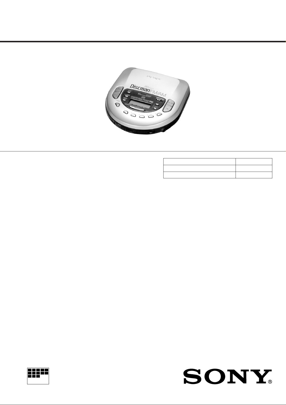
Photo : D-T401
SPECIFICATIONS
US Model
Canadian Model
D-T401/T405
AEP Model
UK Model
E Model
Chinese Model
Australian Model
D-T101/T401/T405
Tourist Model
D-T405
Model Name Using Similar Mechanism D-265/365
CD Mechanism Type CDM-2811CAA
Optical Pick-Up Name DAX-11C
CD player section
System
Compact disk digital audio system
Laser diode properties
Material:GaAIAs
Wavelength:λ=780nm
Emission duration:Continuous
Laser output:less than 44.6uW (measured at 200mm
away from the objective lens surface)
Error correction
Sony Super Stlategy Cross Interleave Reed Solomon Code
D-A conversion
1-bit quartz time-axis control
Frequency response
20-20,000Hz
Output(at 4.5V input level)
Headphones (stereo minijack)
Line output (stereo minijack)
Optical digital output (optical output connector)
Radio section
Frequency range
FM:87.5-108.0MHz
AM:531-1,602kHz
Antenna
FM:Headphones coad antenna
AM:Built-in ferrite bar antenna
+1
dB (measured by EIAJ CP-307)
–2
15mW+15mW at 16ohms
Output level 0.7Vrms at 50kilohms
Recommended load impedance over 10 kilohmes
Output level–21–15dBm
Wavelength:630-690nm at peak level
Genaral
For the area code of the model you purchased,
check the upper left side of the bar code on the
package.
Power requirements
• Sony BP-DM10 Rechargeable battery:
2.4V DC,Ni-Cd,650mAh
Sony BP-DM20 Rechargeable battery:
2.4V DC,Ni-MH,1,200mAh
• Two LR6 (Size AA) batteries:3 V DC
• AC power adaptor (DC IN 4.5V jack)
US/CND/E92model:220-230V, 50/60Hz
UK model:230-240V,50Hz
EA model:110-240V,50/60Hz
AUS model:240V,50Hz
JEW/E33 model:100-240V,50/60Hz
• Sony CPM-300P mount plate for use on car
battery:4.5 V DC
Dimensions(w/h/d) (without projecting parts and
controls)
Approx.132×34.0×135.6
1
(5
/4×11/4×53/8in.)
Mass (without rechargeable battery)
Approx.280g (9.9oz)
Operating temperature
5°C-35°C (41°F-95°F)
Supplied accessories
T405
For the area code of the model you purchased,
check the upper left side of the bar code on the
package.
AC power adaptor (1)
Head phones (1)
Earphones (1)
Rechargeable battery (1)
Battery case (1)
Connecting cord (phone plug×2↔stereo
miniplaug) (1)
Carrying case (1)
a) Supplied with US model
b) Not supplied US model
c) Not supplied with US,CND and E92 models
d) Not supplied with JEW, AEP, UK and CEF
models
Design and specifications are subject to change
without notice
— Continued on next page —
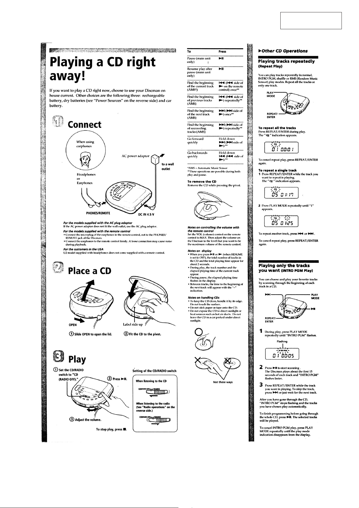
FM/AM COMPACT DISC COMPACT PLAYER

T101
Supplied accessories
AC power adaptor(1)
Earphones(1)
Connecting cord(phone plugx2 stereo miniplug)(1)
T401
AC power adaptor(1)
Headphones(1)
Earphones(1)
Connecting cord(phone plugx2 stereo miniplug)(1)
a)Supplied with US model
b)Not supplied with US model
c)Not supplied with AEP,UK and CEF models
TABLE OF CONTENTS
1. GENERAL ······································································ 4
2. SERVICE NOTE ··························································· 7
3. DISASSEMBLY
3-1. Cabinet (Lower) ································································· 8
3-2. Cabinet (Upper) ·································································· 8
3-3. Tuner Board········································································ 9
3-4. CD Board············································································ 9
Recommended accessories
Mount plate CPM-300P
Mount kit CPM-450PC
Mount kit CPM-300PC
Car connecting pack CPA-9
Car battery cord with car connecting pack
DCC-E26CP
Car battery cord DCC-E245
Active speaker system SRS-A21,SRS-A41,
SRS-A71
Rechargeable battery BP-DM10,BP-DM20
Connecting cord RK-G129HG
Optical digital connecting cord POC-5B
POC-10B,POC-15B,POC-5AB,POC-10AB,POC-15AB
AC power adaptor AC-E45HG
Stereo headphones MDR-35,MDR-E848
Sold in Japan only
Your dealer may not handle some of the above listed accessories.Pleaseask the dealer
for detailed information about the accessories in your country.
NOTE:
In this set, there are a f ormer type (board suffix-12) and a
new type (board suffix-13).
In electrical adjustment, between a former type and a ne w
type, there is a difference of measurement point.
Flexible Circuit Board Repairing
• Keep the temperature of the soldering iron around 270°C during
repairing.
• Do not touch the soldering iron on the same conductor of the
circuit board (within 3 times).
• Be careful not to apply force on the conductor when soldering or
unsoldering.
4. SERVICE MODE ························································ 10
5. ELECTRICAL ADJUSTMENT ······························ 11
6. DIAGRAMS
6-1. Block Diagram –CD Section– ·········································· 16
6-2. Block Diagram –Tuner Section– ······································ 19
6-3. Printed Wiring Board –Tuner Section– ···························· 21
6-4. Schematic Diagram –Tuner Section– ·······························23
6-5. IC Block Diagrams ··························································· 25
6-6. Printed Wiring Board –CD Section – ······························· 26
6-7. Schematic Diagram –CD Section– ···································29
6-8. IC Block Diagrams ··························································· 34
6-9. IC Pin Function ································································ 39
7. EXPLODED VIEWS
7-1. Cabinet Section-1 ·····························································43
7-2. Cabinet Section-2 ·····························································44
7-3. Optical Pick-up Section (CDM-2811CAA) ·····················45
8. ELECTRICAL PARTS LIST ··································· 46
Notes on chip component replacement
• Never reuse a disconnected chip component.
• Notice that the minus side of a tantalum capacitor may be
damaged by heat.
NOTES ON LASER DIODE EMISSION CHECK
The laser beam on this model is concentrated so as to be focused
on the disk reflective surface by the objective lens in the optical
pick-up block. Therefore, when checking the laser diode emission,
observe from more than 30cm away from the objective lens.
SAFETY-RELATED COMPONENT WARNING!!
COMPONENTS IDENTIFIED BY MARK ! OR DOTTED LINE WITH
MARK ! ON THE SCHEMATIC DIAGRAMS AND IN THE PARTS
LIST ARE CRITICAL TO SAFE OPERATION. REPLACE THESE
COMPONENTS WITH SONY PARTS WHOSE PART NUMBERS
APPEAR AS SHOWN IN THIS MANUAL OR IN SUPPLEMENTS
PUBLISHED BY SONY.
— 2 —
ATTENTION AU COMPOSANT AYANT RAPPORT
À LA SÉCURITÉ!
LES COMPOSANTS IDENTIFÉS PAR UNE MARQUE ! SUR LES
DIAGRAMMES SCHÉMATIQUES ET LA LISTE DES PIÈCES SONT
CRITIQUES POUR LA SÉCURITÉ DE FONCTIONNEMENT. NE
REMPLACER CES COMPOSANTS QUE PAR DES PIÈSES SONY
DONT LES NUMÉROS SONT DONNÉS DANS CE MANUEL OU
DANS LES SUPPÉMENTS PUBLIÉS PAR SONY.
SECTION 1
GENERAL
This section is extracted
from instruction manual.
— 3 —
— 4 —
— 5 —
— 6 —
SECTION 2
SERVICE NOTE
NOTES ON HANDLING THE OPTICAL PICK-UP
BLOCK OR BASE UNIT
The laser diode in the optical pick-up block may suffer electrostatic
breakdown because of the potential difference generated by the
charged electrostatic load, etc. on clothing and the human body.
During repair, pay attention to electrostatic breakdown and also use
the procedure in the printed matter which is included in the repair
parts.
The flexible board is easily damaged and should be handled with
care.
NOTES ON LASER DIODE EMISSION CHECK
The laser beam on this model is concentrated so as to be focused on
the disc reflective surface by the objective lens in the optical pickup block. Therefore, when checking the laser diode emission,
observe from more than 30 cm away from the objective lens.
Before Replacing the Optical Pick-Up Block
Please be sure to check thoroughly the parameters as par the “Optical
Pick-Up Block Checking Procedures” (Part No.:9-960-027-11)
issued separately before replacing the optical pick-up block.
Note and specifications required to check are given below.
• FOK output: IC501!™ pin
When checking FOK, remove the lead wire to disk motor.
• S curve P-to-P value: 1.0-2.8Vp-p IC501#¡pin
When checking S curve P-to-P value, remove the lead wire to
disc motor.
• RF signal P-to-P value: 0.8-1.2Vp-p
• Traverse signal P-to-P value: 1.2Vp-p
• The repairing grating holder is impossible.
Precautions for Checking Emission of Laser Diode
Laser light of the equipment is focused by the object lens in the
optical pick-up so that the light focuses on the reflection surface of
the disc. Therefore, be sure to keep your eyes more then 30 cm
apart from the object lens when you check the emission of laser
diode.
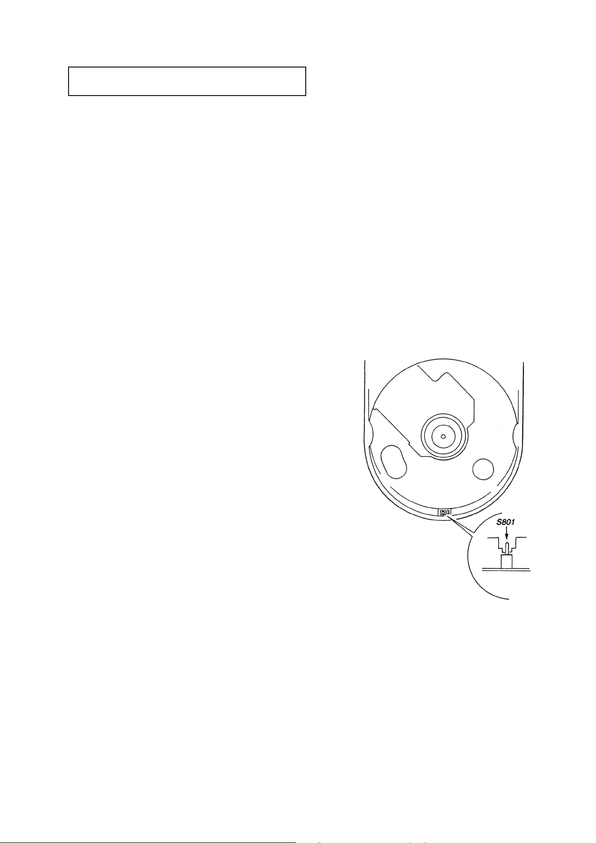
Laser Diode Checking Methods
During normal operation of the equipment, emission of the laser
diode is prohibited unless the upper panel is closed while turning
ON the S801 (push switch type).
The following two checking methods for the laser diode are operable.
• Method (In the service mode or normal operation):
Emission of the laser diode is visually checked.
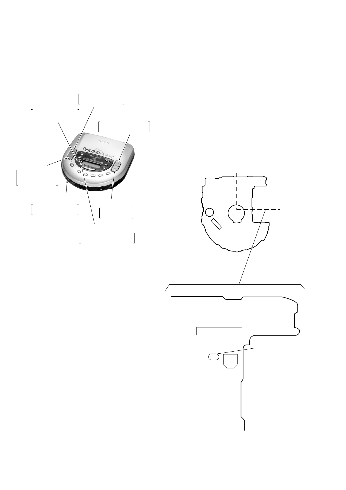
1. Open the upper lid.
2. Push the S801 as shown in Fig. 1.
3. Check the object lens for confirming normal emission of the
laser diode. If not emitting, there is a trouble in the automatic
power control circuit or the optical pick-up.
During normal operation, the laser diode is turned ON about
2.5 seconds for focus searching.
— 7 —
Fug. 1 Method to push the S801
SECTION 3
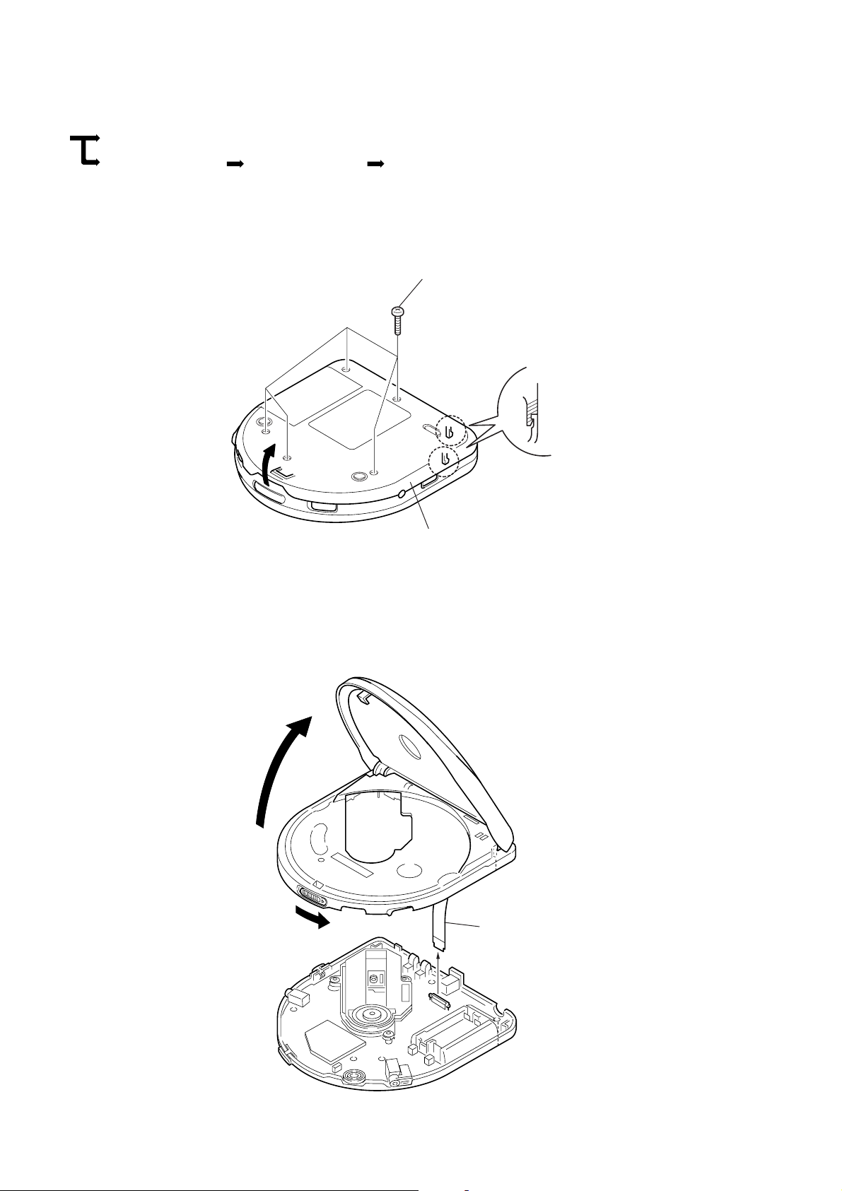
DISASSEMBLY
Note : Follow the disassembly procedure in the numerical order given.
SET TUNER BOARD
CABINET (LOWER) CABINET (UPPER) CD BOARD
3-1. CABINET (LOWER)
1
five screws (B2X10)
2
two clows
3-2. CABINET (UPPER)
3
CABINET (LOWER)
1
PC BOARD, FREXIBLE
— 8 —
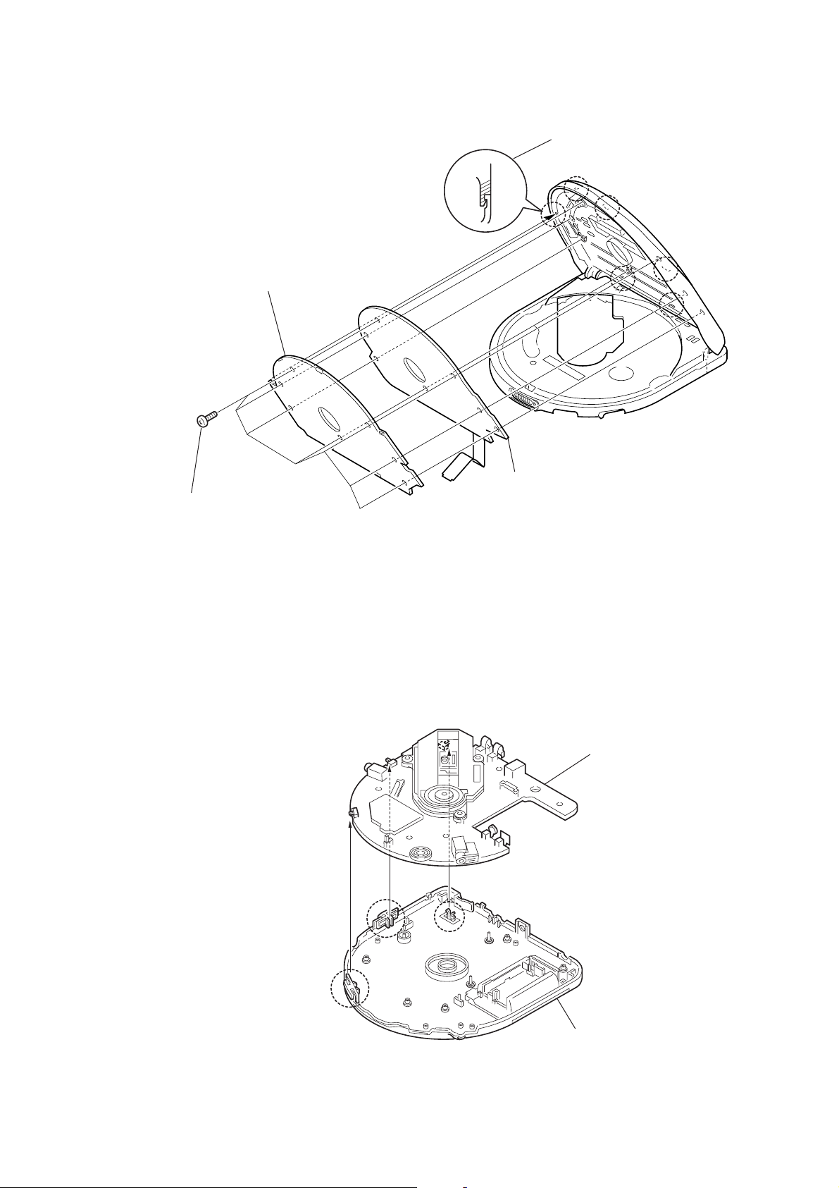
3-3. TUNER BOARD
2
1
SEVEN SCREWS
COVER, LID
3
4
TUNER BOARD
RELEASE THE CLAW
3-4. CD BOARD
1
CD BOARD
CABINET LOWER
— 9 —
SECTION 4
SERVICE MODE
Service Mode (Service program)
The equipment is provided with a service program built in the
microcomputer, like conventional models.
Service program operation methods are described in the following.
+
(FF)
The optical pick-up
REPEAT/ENTER
Tracking gain-up
mode while pressing
=
(FR)
The optical
pick-up is moved
inwardly
HOLD OFF → ON
Be sure to turn OFF
the HOLD switch
(If ON, pressing each
key is deactivated)
is moved outwardly
^
(PLAY/PAUSE)
Focus is turned ON to
effect draw-in mode
p
(STOP)
All servos are
turned OFF
PLAY MODE
Tracking servo and sled
servo are turned ON
4. By pressing the ^ key, focus is turned ON from focus
searching while entering CLV-S (pull-in mode).
Without disk, focus searching is repeated continuously.
5. By-pressing the PLAY MODE key, tracking servo, sled servo
and CLV-A (servo in PLAY) are turned ON.
6. When 4. an 5. are performed, playing begins. No muting is ON
in the service mode.
7. By pressing the p key, all servos (focus, tracking and sled) are
turned OFF. However, the disc motor revolver for a while by
inertia.
• Step 3 (Resetting of service mode)
1. Be sure to disconnect the external power supply and remove
the solder bridge at the TEST terminals connected before in
setting.
2. The set thus becomes available for normal operation.
—CD BOARD— (Component Side)
Description in [ ] indicate major operations in the service
mode. For more informatrion, see Step 2.
Fig. 1 Layout of each key
• Step 1 (Service mode setting methods)
1. Turn OFF the HOLD switch with external power supply
disconnected (power is not applied to the set).
2. Solder across the TEST terminals (TAP802) (pin %¢, IC801
(TEST) is grounded).
3. Connect an external power supply.
Thus, the set is switched to the service mode.
• Step 2 (Operation in the service mode)
1. Once the service mode is effected, the LCD display 5 indications
each of which is repeatedly displayed.
However, the following oprations can be activated even if LCD
indication is effected.
2. By pressing the + or = key , the optical pick-up is movable
inwardly or outwardly. However, if this is activated, tracking
servo and sled servo are turned OFF , so it can be turned ON by
pressing the PLAY MODE key if required.
3. By pressing the REPEAT/ENTER key, the tracking gain-up
mode becomes active.
CN801
TAP802
(TEST)
C409
— 10 —
SECTION 5
ELECTRICAL ADJUSTMENTS
CD SECTION
Precautions for Adjustment
1. Before beginning adjustment, set the equipment to service mode.
After the completion of adjustment, be sure to reset the service
mode.
For more information, see “ Service Mode (service program) ”
on page 10.
2. Perform adjustments in the order given.
3. Use YEDS-18 disk (Part No.:3-702-101-01) unless otherwise
indicated.
4. Power supply voltage requirement: DC2.5V in battery terminal
HOLD switch : OFF
VOLUME : Minimum
ESP switch : OFF
BASS BOOST switch : NORM
AVLS switch : OFF
RESUME switch : OFF
Before Beginning Adjustment
Set the equipment to service mode (See page 10) and check the
following. If there is an error, repair the equipment.
• Checking of the sled motor
1. Open the upper panel.
2. Press the + and = keys and check that the optical pick-up
can move smoothly without sluggishness or abnormal noise in
innermost periphery → outermost periphery → innermost
periphery
+ :The optical pick-up moves outwardly.
= :The optical pick-up moves inwardly.
Adjustment Location: CD board (See page 14.)
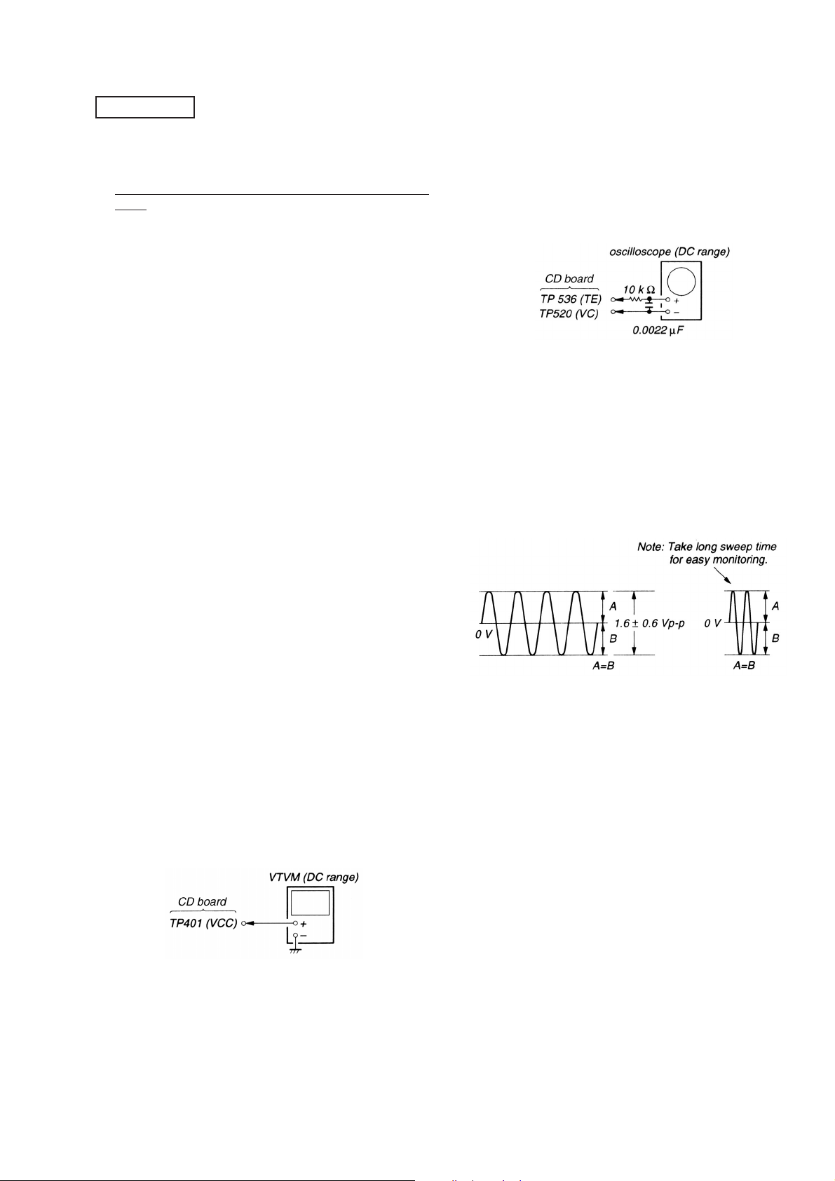
Tracking Balance Adjustment
Condition:
• Hold the set in horizontal state.
Adjustment Procedure:
1. Connect the oscilloscope to TP536 (TE) of the CD board.
2. Connect TP562 to TP520 (VC) of the CD board.
3. Set the equipment to service mode stop state. (See page 10.)
4. Move the optical pick-up by pressing the + and =keys.
5. Put the disk (YEDS-18).
6. Press the ^ key.
From focus searching, focus is turned ON while entering
[
CLV drawing-in mode. Tracking and sled are turned OFF.
7. Adjust RV501 so that the waveform on the oscilloscope becomes
up/down symmetrical with an axis of 0V.
]
• Checking of focus searching
1. Open the upper panel.
2. Press the + key. (Focus searching operation is activated
continuously.)
3. Check the object lens of the optical pick-up for smooth up/down
motion without sluggishness or abnormal noise.
4. Press the p key.
Check that focus searching operation is deactivated. If not, again
press the p key slightly longer.
VCC Adjustment
Adjustment Procedure:
1. Set the equipment to service mode stop state. (See page 10.)
2. Connect the VTVM to TP401 (VCC) of the CD board.
3. Adjust RV401 on the CD board so that the reading on VTVM
goes 2.75±0.05V.
4. After the completion of adjustment, reset service mode. (See
page 10.)
8. Stop removing of the disk motor by pressing the p key.
9. After adjustment, disconnect between TP562 and TP520 (VC)
and release the service mode. (See page 10.)
Adjustment Location: CD board (See page 14.)
— 11 —
Focus bias Check
Condition:
• Hold the set in horizontal state.
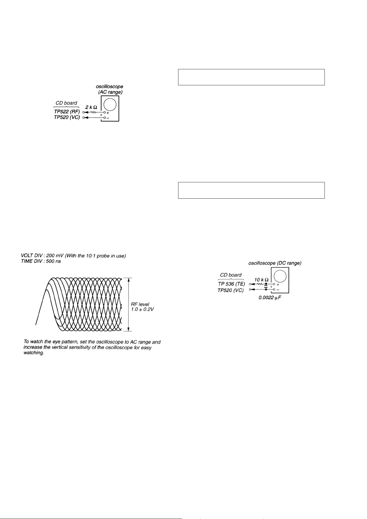
Focus/Tracking Gain Adjustment
A servo analayzer is necessary in order to perform this adjustment
exactly.
Check Procedure:
1. Set the equipment to service mode stop state. (See page 10.)
2. Connect the oscilloscope to the test point TP522 (RF) of the
CD board.
3. Move the optical pick-up by pressing the + and = keys.
4. Put the disc (YEDS-18).
5. Press the ^ key.
From focus searching, focus is turned ON while entering
[
CLV drawing-in mode. Tracking and sled are turned OFF.
6. Press the PLA Y MODE key. (Both tracking and sled are turned
ON.)
7. Check the oscilloscope waveform is as shown below.
A good eye pattern means that the diamond shape (≈) in the
center of the waveform can be clearly distinguished.
RF SIGNAL REFERENCE WAVEFORM (EYE PATTERN)
However, this gain has a margin, so even if it is slightly off,
there is no problem. Therefore, do not perform this adjustment.
Focus/tracking gain determines the pick-up follow-up relative to
mechanical noise and mechanical shock when the 2-axis device
operates. However, as these reciprocate, the adjustment is at the
point where both are satisfied.
• When gain is rased, the noise when 2-axis device operates
increase.
• When gain is lowered, it is more susceptible to mechanical shock
and skipping occurs more easily.
This adjustment has to be performed upon replacing any of the
following parts.
• Optical pick-up
• RV503 (Focus gain VR)
• RV502 (Tracking gain VR)
]
Normally, be sure not to move RV503 (focus gain VR) and
RV502 (tracking gain VR).
Adjustment method:
– Focus Gain Adjustment –
This adjustment is not performed.
If focus gain VR RV503 is turned, set to mechanical center.
– Tracking Gain Adjustment –
(perform at normal operation)
8. Stop revolving of the disk motor by pressing the p key.
9. After the completion of adjustment, reset service mode. (See
page 10.)
Check Location: CD board (See page 14.)
1. Place the optical pick-up level, horizontally. (If the optical pickup is not level, the 2-axis device will be weighted and adjustment
cannot be done.)
2. Connect the oscilloscope TP536 (TE) and TP520 (VC) on CD
board.
3. Set the disk (YEDS-18) and press the ( (+) key.
4. Turn R V502 slightly clockwise (tracking gain drops) and obtain
a waveform with a fundamental wave (waveform has large
waves) as in Figure 1.
5. Turn R V502 slowly counterclockwise (tracking gain rises) until
the fundamental wave disappears (no large waves) as in Figure
2.
6. Set R V502 to the position about 30° counterclockwise form the
position obtained in step 5. If RV502 contact point is more than
90° counterclockwise from mechanical center, tracking gain is
too high. In this case, readjust from step 4.
7. Press ( (+) or = key and observe the 100 track jump
waveform. Check that no traverse waveform appears for both
( (+) or = key and observe the 100 track jump
waveform. Check that no traverse waveform appears for both
( (+) or = directions. (See Figures 3 and 4.) It is
acceptable if the traverse waveform appears only now and then,
but if it appears constantly, raise tracking gain slightly and check
step 7 again.
8. Check that there is not abnormal amount of operation noise
(white noise) from the 2-axis device. If there is, tracking gain is
too high, readjust starting with step 4.
— 12 —
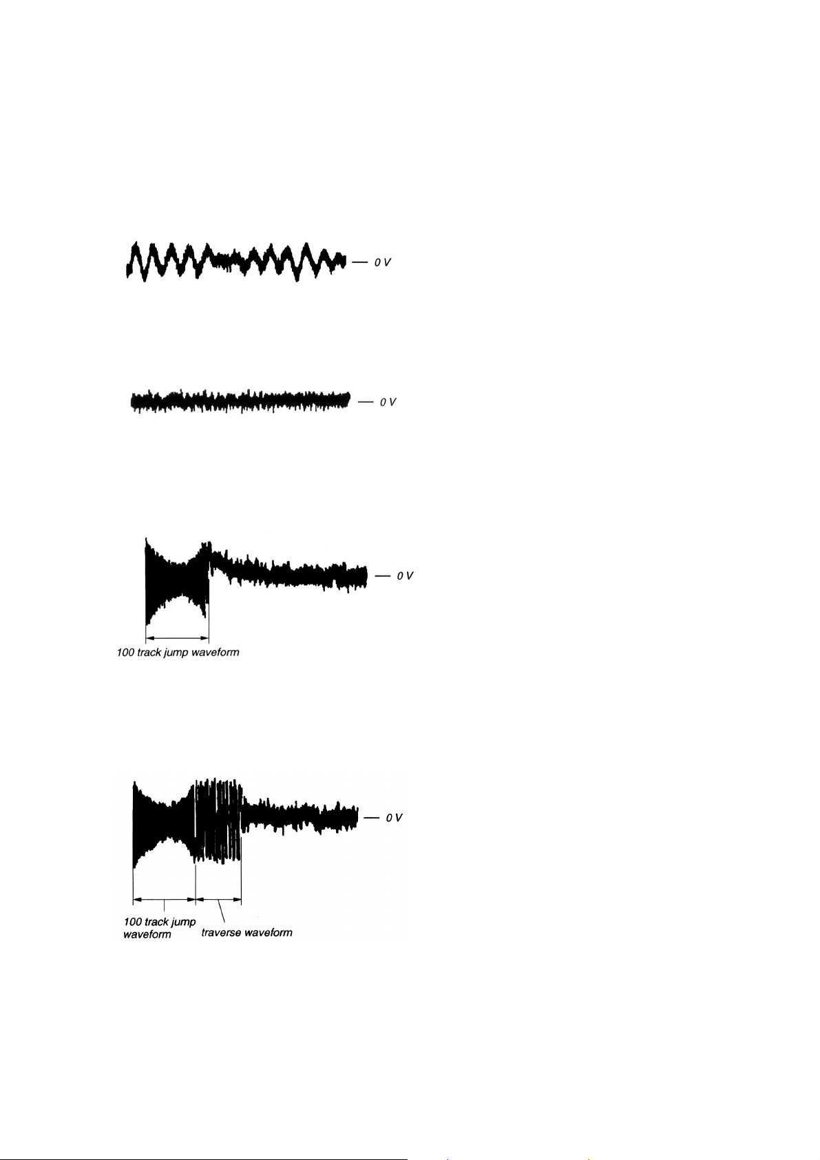
The wavwforms are those measured with the oscilloscope set as
shown below.
• VOLT/DIV : 50mV
• TIME/DIV : 5ms
• Waveform when tracking gain is lowered.
Fundamental wave appears (large waves).
Fig. 1
• W aveform when fundamental wave disappears (no large waves).
Fig. 2
• Waveform with no traverse waveform during 100 track jump.
(Brake application is smooth because of adjustment.)
Fig. 3
• Waveform with traverse waveform during 100 track jump.
(Brake application is poor because of adjustment.)
Fig. 4
— 13 —
Adjustment Part Location:
—CD BOARD— (Component Side)
TP562
RV401
VCC
TP522
(RF)
RV501
TRACKING
BALANCE
RV502
TRACKING
GAIN
RV503
FOCUS
GAIN
TP536 (TE)
TP520 (VC)
TP401 (Vcc)
— 14 —
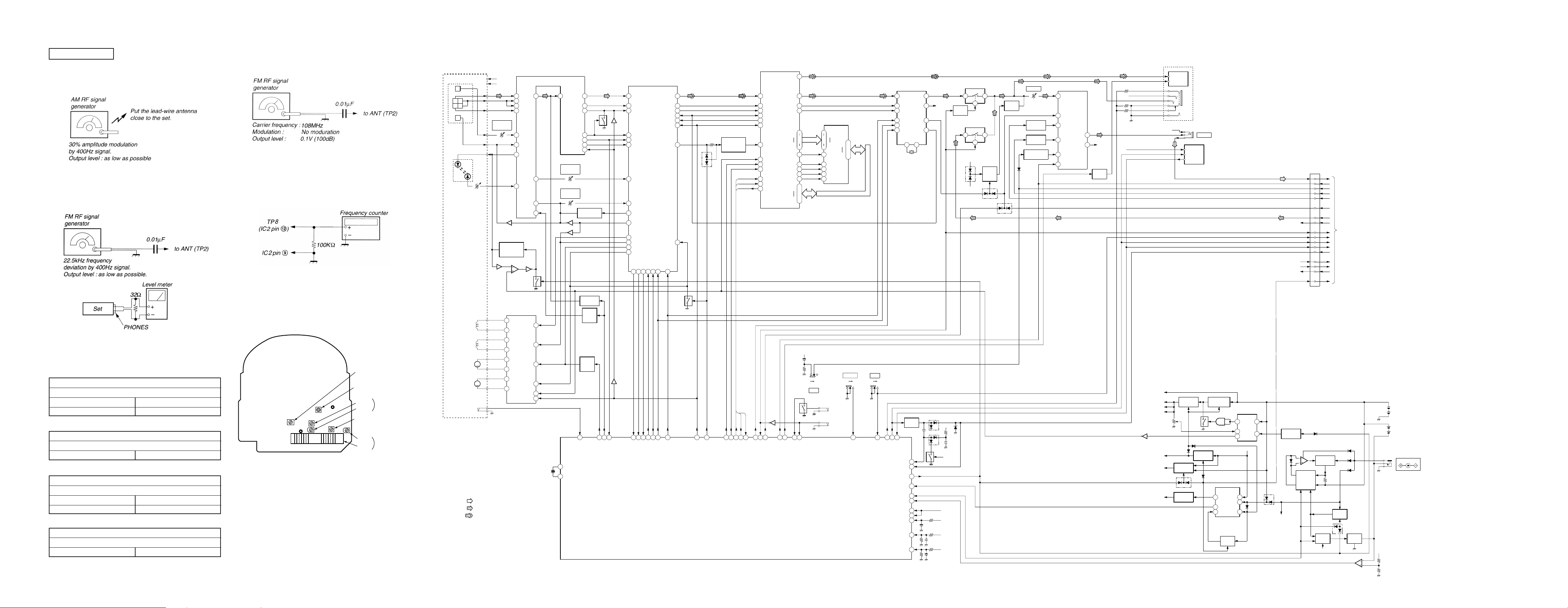
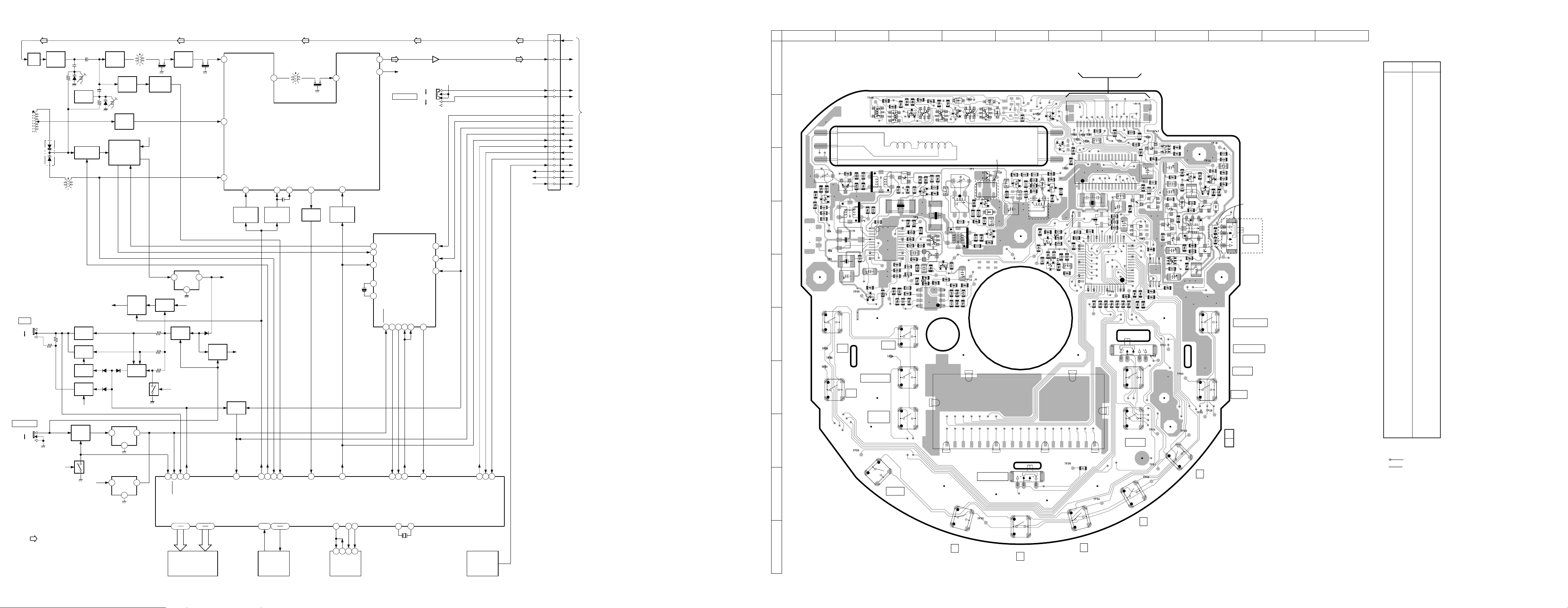
SECTION 6
DIAGRAMS
D-T101/T401/T405
TUNER SECTION
[AM]
BAND switch : AM
[FM]
BAND switch : FM
FM VCO Adjustment
Procedure :
1. Connect the frequency counter to the positions shown below.
2. Turn the set to 108MHz.
3. Adjust RV1 for 19kHz±200Hz reading on the frequency counter .
6-1. BLOCK DIAGRAM — CD SECTION —
OPTICAL PICK-UP BLOCK
(DAX-11C)
DETECTOR
E
A
B
F
PD
A
C,D
C
D
B
E
F
LD
LASER
DIODE
LD
POWER
VCC
VC
28
A
25
C
27
D
26
IC505
4
1
T402
Q420,421
AUTO MATIC
POWER
CONTROL
41
3
B
1
E
2
F
6
LD
7
PD
4
2
RV501
TRACKING
BALANCE
IC404 IC405 IC408
3
23 22
13
FEO
10
TEO
9
DFR
4
Q422
IC501
RF AMP
RFIRFO EFM
MIRR
ASY
DEFECT
FOK
FON
CAGC
RV503
FOCUS
GAIN ADJ
RV502
TRACKING
GAIN ADJ
Q519
Q513,514
16
15
17
14
12
11
4
ESP SWITCH
Q515-517
Q504
IC601
RAM CONTROLLER
CHDT
DATA
BCKO
LRCK
XWE
XRAS
XCAS
XOE
7
IC301
DAC / LPF
16
14
15
IC602
D RAM
41
A0
43
.
40
A8
36
35
A9
33
34
28
27
31
.
D0
32
.
29
.
D3
30
9
A0
12
.
9
14
18
5
3
4
23
22
4
WE
RAS
CAS
OE
1
.
A8
D0
2
.
4
24
.
D3
A9
13
22
23
24
20
19
18
DATA
BCLK
LRCK
SDATA
SHCK
DACLT
XTLI XTLO
15 16
X301
16.9MHz
L OUT
R OUT
LRSL
CKO
9
5
R-CH
11
13
SWITCH
Q308
D302
IC101
SWITCH
IC102
SWITCH
VDD
V IN
RV301
VOLUME
21
4
21
4
MUTE
SWITCH
D301
Q302
D304
MUTE
Q101
BB SWITCH
Q306
LP SWITCH
Q305
ALV SWITCH
Q304
13
L IN
11
MUTE
8
BB SW
9
LP
6
AVC IN
19
BEEP
IC302
HP AMP
L OUT
R OUT R-CH
R-CH
4
2
MUTE
Q602
VDD
IC502
DSP / SERVO
3
EFM
34
MIRR
2
IC506
33
12
15
13
16
76
39
21
22
24
30
ASY
DEFECT
XFOK
FON
FEI
TEI
GFS
SBSO
FE DRV
TE DRV
SL DRV
CLVOPO
SCOR
38
45
BUSY
43
SUBQ
80
COMPC
44RW41
4
3
DATA
BCLK
LRCK
XIN
RFCK
XRST
C2PO
SL IN
SQCK42CDATA
69
70
68
74
36
73
66
23
D601
ESP ON
SHOCK MUTE
Q601
SCK
SDTI
SDTO
11
DATA
13
BCKI
12
CRCI
9
CKO
18
RFCK
20
XRST
17
XRFO
6
C176
22
XSOE
24
XLT
26
SCK
25
SDTI
21
SDTO
J301
OPTICAL
DIGITAL
OUT
REMOTE
CONTROL
J302R-CH
PHONES
FM ANT
T BEEP
XAVLS
TA MUTE
AUDIO L
R-CH
CDSLP
XHOLD
RMDAT
RMKEY
V IN
DC IN
VDD
XTPCON
MB 2
MB 1
KEY
CN801
TO
MAIN BLOCK
• Repeat the procedures in each adjustment several times, and
the frequency coverage and tracking adjustment should be finally
done by the trimmer capacitors.
( ) : U, CA model
AM TRACKING ADJUSTMENT
Adjust for a maximum reading on level meter.
L7 702kHz (700kHz)
CT3 1,404kHz (1,400kHz)
( ) : U, CA model
AM VOL T A GE ADJUSTMENT
1.6V±0.1V
T4 531kHz (530kHz)
FM TRACKING ADJUSTMENT
Adjust for a maximum reading on level meter.
L2 87.5MHz (76MHz)
CT2 108MHz
( ) : U, CA model
FM VOL T AGE ADJUSTMENT
3.0V±0.1V (1.0V±0.1V)
L3 87.5MHz (76MHz)
Adjustment Part Location:
[TUNER BOARD] – SIDE A –
TP2
TP8
L3:FM Voltage
Adjustment
RV1:FM VCO
Adjustment
L2 : FM Tracking
CT2: Adjustment
T4:AM Voltage
Adjustment
CT3: AM Tracking
L7 : Adjustment
BUFFER
OSC 1
OSC 2
SWITCH
35
XLMT
Q502,503
LASER
DRIVER
Q518
SLD
Q501
2
SLDON
8
42
ESPO
FOK
Q507
45
43
SCOR
23
BUSY
62
SUBQ
26RW6
COMPC
IC504
MOTOR DRIVER
FOCUS
COIL
TRACKING
COIL
M901
SLED
MOTOR
M902
SPINDLE
MOTOR
S901
16
LIMIT SW
FCS+
FCS-
TRK+
TRK-
M
CLV+
M
Signal path
: FM
: CD
:DIGITAL OUT
SLED+
SLED-
CLV-
1A
28
FED
TAD
SLD
CLV
CLK
LIM
6
14
3
17
11
9
21
X801
22
1B
30
3B
25
3A
27
2A
33
2B
32
4A
22
4B
23
25
SQCK
24
CDATA
Q510
VDD
S803
NORMAL
LIMIT OFF ON
S301
ALVS
Q802
SDTO
9
46
DACLT
28
CDSLP
Q803
A MUTE
44
6
BEEP
33
OP MUTE
32
OPEN
XRCHG
SCK
SDTI
SDTO
40
30
10
XRST
C2POEN
IC801
CD SYSTEM
CONTROL
39
38
37
41
XLT
SCK
SDTI
XSOE
RESUME
OFF ON
S801
LID OPEN
DETECT SW
S802
RECHG BATT
DETECT SW
34
XRSM
S804
HOLD
31
XHOLD
54
12
ESPSL
RMDAT56RMKEY
WP
KEY
P CON
RESET
CHGON
CHG MNT
VDD
VDD
VCC MNT
BAT MNT
DC IN MNT
SWITCH
Q801
36
55
27
20
11
59
1
47
61
58
57
D804
D803
Q413
VDD
DC IN
VDD
VCC
V IN
DC IN
OSC
IC407
42
IC101,102 B+
IC302 B+
IC404,405
IC407,408
V IN
DVDD
AVDD
VCC
B+ SWITCH
Q309
D307
T401
DC/DC
CONVERTER
IC409
4
IC406
RESET
5
VOUT
3
VDOUT
CE
SWITCH
Q414
V IN
BATTERY CASE
LR6 x 2
ALKALINE BATT
LR6 x 2
RECHG BATT PACK
BP-DM10/DM20
J401
DC IN 4.5V
IC401
1
5
2
VDIN
LX
VDD
3
CD
REG
1
2
7
VDD
4
8
62
D411
SWITCHING
DC IN
Q412,415
IC403(1/2)
ERROR AMP
8
5
6
CURRENT
PROTECT
&
SWITCH
Q409,410
D404
D414
D405
SWITCH
Q407
D401
D403
SWITCH
Q405,406
IC403(2/2)
2
1
3
AMP
REG
7
Q403,404
SWITCH
Q408
VDD
RECTIFIER
Q401
Q402RV401
D407
D308
B+ SWITCH
Q301,307
D305
B+ SWITCH
B+
Q303
– 15 – – 16 – – 17 – – 18 –
D-T101/T401/T405
12
A
B
C
D
E
F
G
H
I
J
34567891011
PLAY/PAUSE
S21
STEP
S11
MEGABASS
S12
STOP
S24
TUNE–
S5
C96
TUNE+
S1
S12
S1
5
S8
S8
4
S4
S4
3
S7
S7
2
S3
S3
FUNCTION
S10
ND1
1
S6
S6
BAND
S2
PLAYMODE
S25
ESP
S28
FR
S22
FF
S23
REPEAT
/ENT
S26
TO CD BOARD
CN801
C61
C64
R41
C69
Q33
Q32
R61
R62
C65
R38
R45
C27
C67
C68
C72
Q24
Q22
C44
Q19
Q17
R36
L9
Q20
R34
R35
R37
C66
Q23
C34
D8
D9
D10
C43
R42
C88
R48
JC7
C33
D6
S11
R57
R58
Q35
L8
R112
R55
R87
R74
C74
C52
R21
R86
C93
C94C90
C89
C80
R68
R8
Q29
C16
CN1
L5
C86
C82
IC5
C22
R79
R73
R67
R72
R71
R24
R80
R81
R82
R83
R84
R85
R63
R64
R65
R66
Q30
C70
C85
Q31
R10
D4
L3
C15
C12
L12
C14
L6
C87
C81
L11
R70
X1
X2
IC8
IC4
L10
IC3
R32
R60
Q44
C73
S21
S24
C75
IC6
R114
R39
C62
R40
C63
C20
C21
C13
C23
R6
TP2
R9
C19
C18
Q4
Q3
R4
R2
Q2
C11
L4
C6
L1
R1
C8
R12
C25
C26
R31
C38
C37
C35
R22
C32
D3
R16 R18
R19
C29
R20
Q7
C41
C28
C30
CT3
T2
CF2
C45
R23
R13
R14
R52
R56
R54
R115
R113
CF1
C9
R5
C10
C104
R101
C101
Q11
C53
RV1
R27
R90
C55
C54
C48
C46
R30
IC2
C103
R93
IC7
R94
C92
C36
TP8
Q12
C42
R100
C100
C102
R97
R96
Q1
FL1
D1
D5
C7
T1
CT2
Q5
R11
C24
Q16
Q39
Q43
R44
R51
R50
R53
Q40
Q36
Q37 Q42
Q41
Q38
L7
D14
D16
R47
D15
C99
R92
R102
R103
R99
R91 R98
C59
C51
C50
C56
R29
C47
CF4
T4
C39
Q10
R28
R26
R25
C49
C40
CF3
C58
C57
C60
Q28
C17
R43
C98
C31
JC8
C18,L3
T101,T401
EXCEPT T405:JEW
AEP,IT,UK/T101:EA
E13,E33,E92,AUS,CN
/T401:US,CND
/T405:US,CND,JEW
EXCEPT T101:US,CND
/T401:EA,JEW
/T405:EA
1–665–577–
11
(11)
6-2. BLOCK DIAGRAM — TUNER SECTION —
T1
Q2
FM OSC
BUFFER
Q4
L3
FM OSC
MW RF
AMP
Q7
DC/DC
CONVERTER
T3,Q22-24,
Q35,44
FM IFT
V IN
FM RF
B.P.F
AMP
FL1
L7
AM FERRITE-ROD
ANTTENA
D3
Q1
T4
AM OSC
L2
FM RF
FM OSC
Q3
L.P.F
Q17,19,20
FM MIX
AMP
Q37
Q36
Q40
Q38
VDD
Q43
(1/2)
VDD
B+
RESET
2 1
IC1
3
RESET
2 1
IC4
3
FM FE
POWER
SWITCH
Q16
SWITCH
Q39
@@@
Q43
(2/2)
S11
STEP
9k
10k
S10
FUNCTION
RADIO
CD
Signal path
: FM
16
DC IN
SWITCH
SWITCH
SWITCH
SWITCH
RESET
SWITCH
Q13,14
CF1
FM LOSC
BUFFER
Q31
FM IF
AMP
CF4
3
Q5
FM IF IN
MIX
T1
AM IFT
4
CF2
450kHz
6
AM IF IN
IC2
8
AM RF IN
Q32,33
REG
2
SWITCH
DC IN
Q28
REG
IC3
1
V IN
2
OSC
LPF1 LPF2A LPF2B IF OUT IF REQ
16 19 18 10
3
D6
B+
SWITCH
Q29
VDD
SWITCH
Q41,42
IC7 B+
Q11
VCO STOP
SWITCH
FM-MW
SWITCH
Q10
50 12 2 194 20 21 56
RESET
XDC IN
AREASL
BAT MNT
COM0-3 LCD0-14 KEYI KEYO
34
31 1110
4935 96
LCD
ND1
– 19 – – 20 – – 21 – – 22 –
13 55 511
EQ
RM KEY
AM CTL
.
TUNER
KEY BLOCK
S1-S8
FM IF/DET
MPX MW RF/MIX/DET
VCO L
VCO H
IC5
DTS MICOM
IF AMP
Q30
17 1654
FM IFC
11
IF
REQUEST
Q112
DI/DO
14 5
3 4 1 2
DI
EEPROM
4019MHz
MUTE
DO
IC6
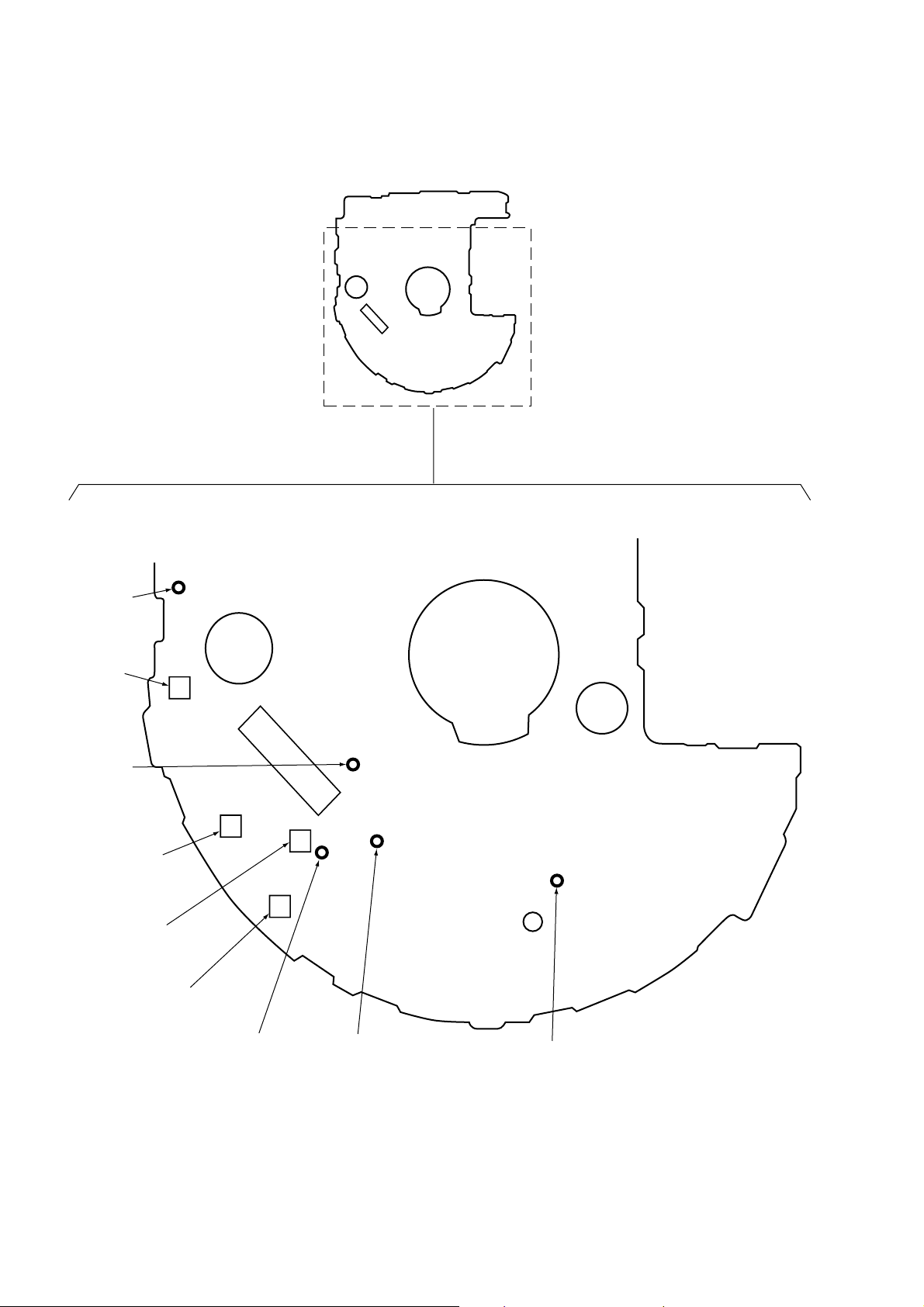
6-3. PRINTED WIRING BOARD — TUNER SECTION —
FM ANT
IC7
LINE AMP
NORM
DDAT IN
XTPCON
CDSLP
RQT
SI
67
MID
MAX
RQ
915
VDD
35
8
14
L OUT
15
R OUT
7 21
14
25
2
X2
1
MUTE
MUTE
X1
X2
MEGABASE
I/F MICOM
RESET
SO
16 174 22
R-CH
S12
IC8
CLK
DC IN
V IN
VDD
AUDIO L
MB1
MB2
RM DATA
XTPCON
CDSLP
RM KEY
TU MUTE
BEEP
XAVLS
XHOLD
CD KEY
TO
MAIN BLOCK
LCD(SK)
LCD (DAT)
TU RQ
IF RQ
52 53 15
BEEP
XAVLS
XHOLD
CS
SK
3
SK
CS
25
75kHz
XIN
XOUT
24
X1
CD
KEY BLOCK
S21-26,28
• Semiconductor
Location
Ref. No. Location
D1 C-4
D3 C-2
D4 C-5
D5 D-4
D6 C-7
D8 C-8
D9 D-9
D10 D-8
D14 B-4
D15 B-4
D16 B-4
IC2 D-2
IC3 C-7
IC4 D-7
IC5 E-6
IC6 E-7
IC7 E-3
IC8 C-7
Q1 C-4
Q2 D-4
Q3 C-5
Q4 C-5
Q5 C-3
Q7 C-1
Q10 D-3
Q11 E-3
Q12 E-2
Q16 C-3
Q17 C-8
Q19 C-8
Q20 C-8
Q22 D-8
Q23 D-8
Q24 D-8
Q28 B-5
Q29 B-6
Q30 D-5
Q31 E-6
Q32 B-8
Q33 B-7
Q35 D-8
Q36 B-3
Q37 B-3
Q38 B-4
Q39 B-2
Q40 B-3
Q41 B-4
Q42 B-4
Q43 B-2
Q44 E-8
Note:
• : Parts extracted from the component side.
• : Pattern on the side which is seen.
• Abbreviation
E13 : 220-230V (No charger switch) area
E33 : 100-240V (Without VS) area
E92 : 120V area
AUS : Australian
CND: Canadian
CN : Chinese
EA : Saudi Arabia
 Loading...