

Page 1
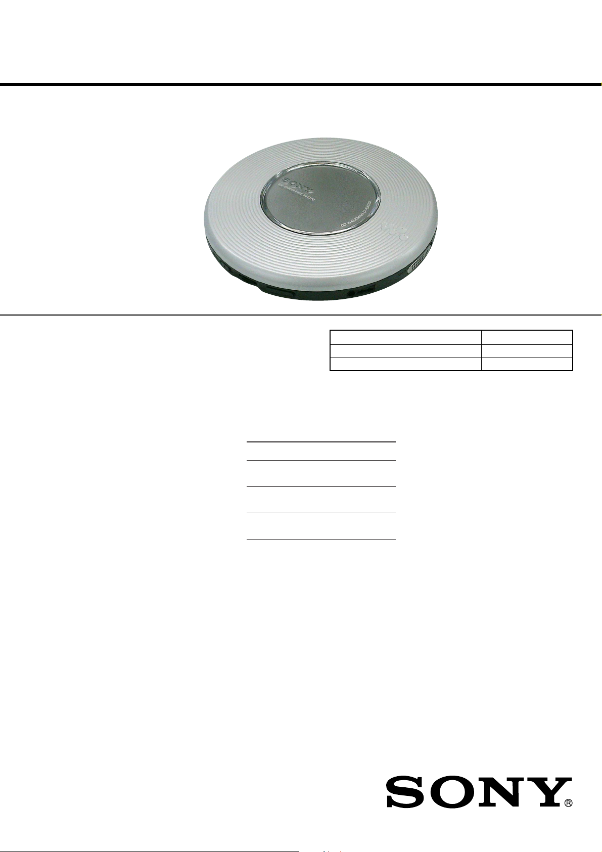
D-EJ785
SERVICE MANUAL
Ver 1.0 2002.12
SPECIFICATIONS
Canadian Model
AEP Model
UK Model
E Model
Austr alian Model
Chinese Model
Tourist Model
Model Name Using Similar Mechanism NEW
CD Mechanism Type CDM-3325ER
Optical Pick-up Name DAX-25E
System
Compact disc digital audio system
Laser diode properties
Material: GaAlAs
Wavelength: λ = 780 nm
Emission duration: Continuous
Laser output: Less than 44.6 µW (This output is the value
measured at a distance of 200 mm from the objective lens
surface on the optical pick-up block with 7 mm aperture.)
Power requirements
For the area code of the model you purchased, check the
upper left side of the bar code on the package.
•Sony NH-WM2AA rechargeable batteries: 2.4 V DC
•Two LR6 (size AA) batteries: 3 V DC
•AC power adaptor (DC IN 4.5 V jack):
Canadian and Taiwan models: 120 V, 60 Hz
UK model: 230 V, 50 Hz
Australian model: 240 V, 50 Hz
AEP, East European, E, Korean and Tourist models:
100 - 240 V, 50/60 Hz
Hong Kong model: 230 V, 50/60 Hz
Chinese model: 220 V, 50 Hz
Battery life* (approx. hours)
(When the CD player is used on a flat and stable place.)
Playing time varies depending on how the CD player is
used.
G-PROTECTION
on off
Two NH-7WMAA 15 10
(charged for
about 2 hours**)
NH-WM2AA 32 24
(charged for
about 4 hours**)
Two Sony alkaline 50 35
batteries LR6 (SG)
(produced in Japan)
*Measured value by the standard of JEITA (Japan
Electronics and Information Technology Industries
Association).
** Charging time varies depending on how the
rechargeable battery is used.
Dimensions (w/h/d) (without projecting
parts and controls)
Approx. 136.0 × 19.6 × 136.0 mm (5 3⁄
Mass (excluding accessories)
Approx. 155 g (5.5 oz)
Operating temperature
5°C - 35°C (41°F - 95°F)
Supplied accessories
AC power adaptor (1)
Headphones/earphones with remote control (1)
Rechargeable batteries (2)
Battery carrying case (1)
Design and specifications are subject to change without
notice.
× 25⁄32 × 5 3⁄8 in.)
8
9-874-272-01 Sony Corporation
2002L0500-1 Personal Audio Company
C 2002.12 Published by Sony Engineering Corporation
PORTABLE CD PLAYER
Page 2

D-EJ785
TABLE OF CONTENTS
1. SERVICING NOTES............................................... 3
2. GENERAL ................................................................... 6
3. DISASSEMBLY
3-1. Disassembly Flow........................................................... 7
3-2. Spring (A)/(B) ................................................................. 7
3-3. Lid (Upper) Sub Assy ..................................................... 8
3-4. Cabinet (Front) Block ..................................................... 8
3-5. Optical Pick-up Section (CDM-3325ER),
MAIN Board ................................................................... 9
4. ELECTRICAL CHECK .......................................... 10
5. DIAGRAMS
5-1. Block Diagram – MAIN Section –................................ 11
5-2. Block Diagram
– AUDIO/PO WER SUPPLY Section – .......................... 12
5-3. Note for Printed Wiring Boards and
Schematic Diagrams ....................................................... 13
5-4. Printed W iring Board
– MAIN Board (Component Side) – .............................. 14
5-5. Printed W iring Board
– MAIN Board (Conductor Side) – ................................ 15
5-6. Schematic Diagram – MAIN Board (1/3) –.................. 16
5-7. Schematic Diagram – MAIN Board (2/3) –.................. 17
5-8. Schematic Diagram – MAIN Board (3/3) –.................. 18
5-9. IC Pin Function Description ........................................... 21
On AC power adaptor
• Use only the AC power adaptor supplied. Do not use
any other AC power adaptor. It may cause a
malfunction.
Polarity of the plug
Notes on chip component replacement
•Never reuse a disconnected chip component.
• Notice that the minus side of a tantalum capacitor may be dam-
aged by heat.
Flexible Circuit Board Repairing
•Keep the temperature of the soldering iron around 270 ˚C dur-
ing repairing.
• Do not touch the soldering iron on the same conductor of the
circuit board (within 3 times).
• Be careful not to apply force on the conductor when soldering
or unsoldering.
CAUTION
Use of controls or adjustments or performance of procedures
other than those specified herein may result in hazardous radiation exposure.
6. EXPLODED VIEWS
6-1. Front Cabinet Section ..................................................... 26
6-2. Rear Cabinet Section ...................................................... 27
6-3. Optical Pick-up Section (CDM-3325ER)....................... 28
7. ELECTRICAL PARTS LIST ............................... 29
SAFETY-RELATED COMPONENT WARNING!!
COMPONENTS IDENTIFIED BY MARK 0 OR DOTTED
LINE WITH MARK 0 ON THE SCHEMATIC DIAGRAMS
AND IN THE PARTS LIST ARE CRITICAL TO SAFE
OPERATION. REPLACE THESE COMPONENTS WITH
SONY PARTS WHOSE PART NUMBERS APPEAR AS
SHOWN IN THIS MANU AL OR IN SUPPLEMENTS PUBLISHED BY SONY.
ATTENTION AU COMPOSANT AYANT RAPPORT
LES COMPOSANTS IDENTIFIÉS P AR UNE MARQUE 0
SUR LES DIAGRAMMES SCHÉMATIQUES ET LA LISTE
DES PIÈCES SONT CRITIQUES POUR LA SÉCURITÉ
DE FONCTIONNEMENT. NE REMPLACER CES COMPOSANTS QUE PAR DES PIÈCES SONY DONT LES
NUMÉROS SONT DONNÉS DANS CE MANUEL OU
DANS LES SUPPLÉMENTS PUBLIÉS PAR SONY.
À LA SÉCURITÉ!
2
Page 3
SECTION 1
SERVICING NOTES
D-EJ785
ABOUT CD-Rs/CD-RWs
• This CD player can play CD-Rs/CD-RWs recorded in the Compact Disc Digital Audio (Audio CD) format, b ut playback capability may vary depending on the quality of the disc and the
condition of the recording device.
NOTES ON HANDLING THE OPTICAL PICK-UP
BLOCK OR BASE UNIT
The laser diode in the optical pick-up block may suffer electrostatic breakdown because of the potential difference generated by
the charged electrostatic load, etc. on clothing and the human body .
During repair, pay attention to electrostatic breakdown and also
use the procedure in the printed matter which is included in the
repair parts.
The flexible board is easily damaged and should be handled with
care.
NOTES ON LASER DIODE EMISSION CHECK
The laser beam on this model is concentrated so as to be focused
on the disc reflective surface by the objective lens in the optical
pick-up block. Therefore, when checking the laser diode emission, observe from more than 30 cm away from the objecti ve lens.
BEFORE REPLACING THE OPTICAL PICK-UP BLOCK
Please be sure to check thoroughly the parameters as par the “Optical Pick-Up Block Checking Procedures” (Part No.: 9-960-027-
11) issued separately before replacing the optical pick-up block.
Note and specifications required to check are given below.
LASER DIODE AND FOCUS SEARCH OPERATION
CHECK
During normal operation of the equipment, emission of the laser
diode is prohibited unless the upper lid is closed while turning ON
the S801. (push switch type)
The following checking method for the laser diode is operable.
• Method:
Emission of the laser diode is visually checked.
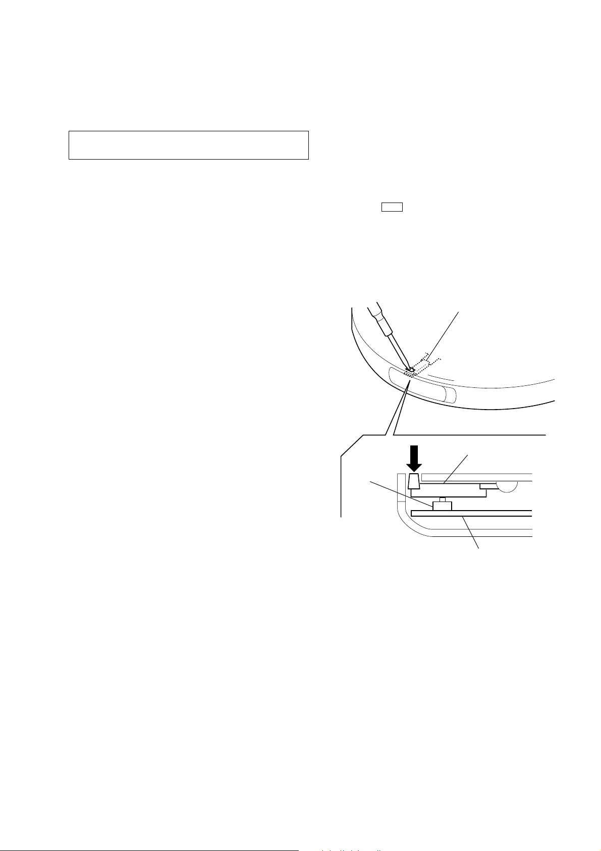
1. Open the upper lid.
2. With a disc not set, turn on the S801 with a screwdri ver having
a thin tip as shown in Fig.1.
3. Press the
4. Observing the objective lens, check that the laser diode emits
light.
When the laser diode does not emit light, automatic power
control circuit or optical pickup is faulty.
In this operation, the objective lens will move up and down 5
times along with inward motion for the focus search.
B X key.
detection lever
• FOK output: IC601 yg pin
When checking FOK, remove the lead wire to disc motor.
• RF signal P-to-P value: 0.45 to 0.65 Vp-p
detection lever
S801
MAIN board
Fig. 1 Method to push the S801
3
Page 4
D-EJ785
SERVICE MODE
In the Service mode, this set can check the following.
Note: Use RM-MC10L (Part No. 1-476-211-
mode. (Use dot matrix Remote Commander)
1. Service Mode Setting Method
To set the service mode, perform as follows.
1) Make sure that the power is not turned on.
2) Check for the following states:
CD lid open detection switch (S801) .... OFF
Solder bridge at TAP802 (OPEN) ......... OPEN
[][]
), when you operate service
[HOLD] switch (S803) .......................... OFF
[AVLS] switch (S808) ........................... OFF
[G-PROTECTION] switch (S802) ........ ON
3) Short the solder bridge at the TAP801 (TEST) on the MAIN
board (see Fig. 2).
4) Turn the power on, and then set a CD.
– MAIN Board (Component Side) –
TAP801
(TEST)
TAP802
(OPEN)
3. Operation of Keys and Knobs in Service Mode
The following operation can be checked by operating the buttons
on the set and remote commander.
• B X key on the set or X key on the remote commander
Focus and tracking/sled servo off
Spindle servo on
Remote Commander LCD display
0000
Note: Do not look directly at the laser beam from the optical pick-up.
(play mode)
[HOLD] switch is on:
Auto adjustment value a becomes as follows each time the key is
pressed.
1) [TRK:MIN:SEC] = RF:FE:TE DC offset adjustment value
2) [TRK:MIN:SEC] = EF: :EF balance adjusted value
3) [TRK:MIN:SEC] = Ga:FG:TG gain adjusted value
[AVLS] switch is on:
Press CHARGE x and B X keys on the set or x and X keys
on the remote commander simultaneously, and RF gain changes
to 0 dB (for normal CD) and +12 dB (for CD-RW).
• . / > keys on the set or B > / . knobs on the
remote commander
Tracking servo off
Optical pick-up movement (outward or inward)
Note: Do not move forcibly the optical pick-up exceeding the most-out-
side or most-inside track.
• CHARGE x key on the set or x key on the remote commander
All servos (focus/tracking/sled) off
• [RPT/ENT] key on the remote commander
Tracking gain up mode
Fig. 2
2. Operation in Service Mode
When the Service mode is set, the LCD on the remote commander
displays the microcomputer version display.
Remote commander LCD display
Microcomputer
version display
All lit
Service mode
VA020
888
DDDD
BASS12
Remote Commander LCD display
Up0000
(For the rest, turn the power off and then turn it on again)
[PLAYMODE] key on the remote commander
•
[HOLD] switch is off:
Spindle speed becomes 1.65/2.0/2.65/3.5 times each time the
key is pressed
Tracking/spindle servo on
Remote Commander LCD display
010001
040004
(For the rest, turn the power off and then turn it on again)
• [SOUND] key on the remote commander
Servo gain adjustment
Tracking servo off
• [DISPLAY] key on the remote commander
On/off switching of the DOUT LED (AEP, UK and East European models) and error rate display
• [VOL +] / [VOL --] keys on the set or remote commander
2-step volume setting
(1.65 times)
(3.5 times)
4
Page 5

4. Service Mode Releasing Method
To release the service mode, perform as follows.
1) Turn the power off.
2) Open the solder bridge at the TAP801 (TEST) on the MAIN
board.
Note: Remove the solder completely.
5.Error Rate Check Display
The C1 error rate check display mode becomes active if the following operation is performed during the operation in the service
mode.
1) Turn the power off, and cancel other service operations.
2) Turn the power on, and then set a CD and play it with
the X key on the remote commander.
Remote Commander LCD display
0000
3) Press the [SOUND] button on the remote commander to make
automatic adjustment.
4) Press the [PLAYMODE] button on the remote commander.
D-EJ785
Remote Commander LCD display
010001
5) Press the [DISPLAY] key on the remote commander, and the
C1 error rate display will be activated and the LCD on the
remote commander will display as follows.
Remote Commander LCD display
Er****
Note: In the play state, press the [SOUND] key on the remote commander
before pressing the [PLAYMODE] key. Wrong order of button operations will result in very large Er**** value.
6) Turn the power off.
7) Open the solder bridges at the TAP801 (TEST) on the MAIN
board.
Note: Remove the solder completely.
**** value
0000 to 0099 : OK
more than 0100 : NG
5
Page 6

D-EJ785
CD player (front)
12 Jog lever (u (play/
pause)•./> (AMS/
search))
3 CHARGE/x •
CHARGE lamp
4 VOL +*/–
SECTION 2
GENERAL
This section is extracted from
instruction manual.
Strap holes
OPEN
A
i (headphones) jack
5 HOLD
*The button has a tactile dot.
**AEP, UK and East European models only
CD player (inside)
6 AVLS
7 G-PROTECTION
Remote control
Display
3x
4 VOL +/–
12 Jog lever (u
B
Open the battery
compartment lid.
(play/pause)•ENT
(enter) • ./>
(AMS/search))
DC IN 4.5 V (external power
input) jack
LINE OUT/LINE OUT (OPTICAL)**
jack
Insert the # end first (for both
batteries).
Display on the remote control
AV LS
Playing time
Track number
Play mode
Clip
5 HOLD
8 DISPLAY
Note
Use only the supplied remote control. You cannot operate
this CD player with the remote control supplied with other
CD players.
9 SOUND
q; P MODE/
Remaining battery power
Sound mode
6
Page 7
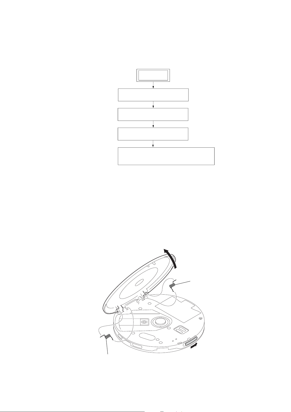
• This set can be disassembled in the order shown below.
)
3-1. DISASSEMBLY FLOW
D-EJ785
SECTION 3
DISASSEMBLY
SET
3-2. SPRING (A)/(B)
(Page 7)
3-3. LID (UPPER) SUB ASSY
(Page 8)
3-4. CABINET (FRONT) BLOCK
(Page 8)
3-5. OPTICAL PICK-UP SECTION (CDM-3325ER),
MAIN BOARD
(Page 9)
Note: Follow the disassembly procedure in the numerical order given.
3-2. SPRING (A)/(B)
2
4
spring (B
3
spring (A)
1
7
Page 8
D-EJ785
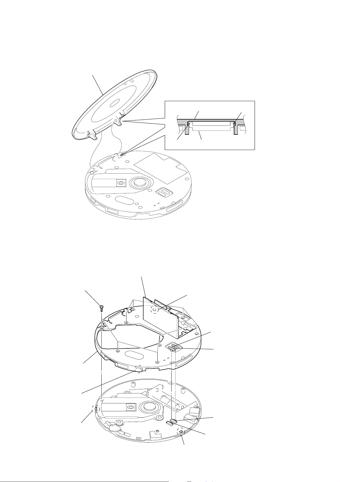
3-3. LID (UPPER) SUB ASSY
3
lid upper sub assy
3-4. CABINET (FRONT) BLOCK
1
Open the lid battery case.
lid upper sub assy
1
boss
2
cabinet front sub assy
boss
2
eight screws (B2)
7
cabinet (front) section
5
claw
4
claw
6
3
claw
knob (AVLS)
knob (G-PRO)
Note : On installation of cabinet (front) assy,
adjust the position of switch (S802)
and knob (G-PRO),
switch (S808) and knob (AVLS).
S802
S808
claw
8
Page 9

3-5. OPTICAL PICK-UP SECTION (CDM-3325ER), MAIN BOARD
qa
main board
4
spacer
6
flexible board
(CN501)
9
insulator
0
optical pick-up section
(CDM-3325ER)
1
screw (B) (1.4)
2
Hold up both the main board and the optical
pick-up section at once, and remove them
form the cabinet (lower) sub assy.
Note : Handle the flexible board with care when
you hold up the optical pick-up section.
Note : On installation of main board,
adjust the position of switch
(S803) and knob (hold).
7
insulator
8
insulator
5
two connectors
(CN502, 503)
3
terminal board
(relay), battery
knob (hold)
S803
D-EJ785
9
Page 10
D-EJ785
p
SECTION 4
ELECTRICAL CHECK
The CD section adjustments are done automatically in this set.
In case of operation check, confirm that focus bias.
PRECAUTIONS FOR CHECK
1. Perform adjustment in the order given.
2. Use YEDS-18 disc (P art No.: 3-702-101-01) unless otherwise
indicated.
3. Power supply voltage requirement: DC4.5 V in DC IN jack.
(J401)
VOLUME : Minimum
[AVLS] switch : NORM
[HOLD] switch : OFF
[G-PROTECTION] switch : ON
FOCUS BIAS CHECK
Condition:
• Hold the set in horizontal state.
Connection:
MAIN board
TP630 (RF)
TP421 (MAINGND)
2 k
Ω
oscilloscope
(AC range)
+
–
Procedure:
1. Connect the oscilloscope to the test points TP630 (RF) and
TP421 (MAINGND) on the MAIN board.
2. Set a disc. (YEDS-18)
3. Press the B X key on the set.
4. Check the oscilloscope waveform is as shown below.
A good eye pattern means that the diamond shape (◊) in the
center of the waveform can be clearly distinguished.
RF Signal reference Waveform (Eye Pattern)
VOLT/DIV : 100 mV (With the 10:1 probe in use)
TIME/DIV : 500 ns
RF level
0.45 to 0.65 Vp-
To watch the eye pattern, set the oscilloscope to AC range and
increase the vertical sensitivity of the oscilloscope for easy watching.
5. Stop revolving of the disc motor by pressing the CHARGE x
key on the set.
Connecting and Checking Location:
– MAIN Board (Conducter Side) –
TP630
(RF)
10
TP421
(MAINGND)
Page 11
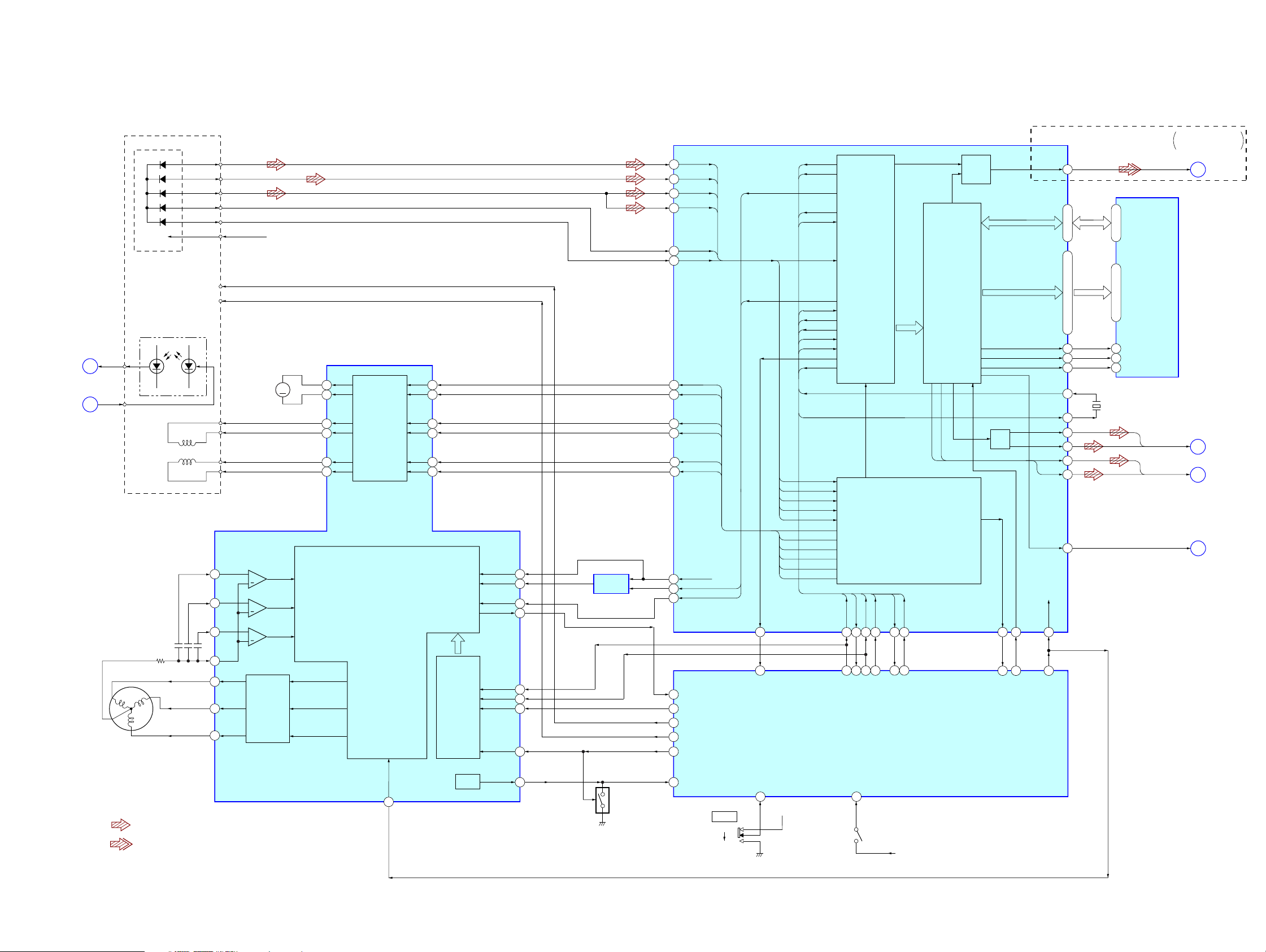
5-1. BLOCK DIAGRAM – MAIN Section –
DETECTOR
A
(Page 12)
B
(Page 12)
OPTICAL PICK-UP BLOCK
LASER DIODE
PD
LD
(FOCUS)
2-AXIS
DEVICE
(TRACKING)
M902
(SPINDLE)
V
U
W
A
B
RF
E
F
VCC
DAX-25E
PD
OPSTB
OPGSW
LD
A
B
RF
E
F
VCC2
M901
M
(SLED)
U1
79
78
77
80
2
4
6
V1
W1
COM
U OUT
V OUT
W OUT
+
+
+
PREDRIVER
SECTION 5
DIAGRAMS
FOCUS/TRACKING COIL DRIVER
SLED/SPINDLE MOTOR DRIVER
IC401 (1/2)
FO1
52
RO1
50
FO2
48
46
44
42
RO2
H BRIDGE DRIVER
FO3
RO3
CONTROLLER,
CONTROL
CIRCUIT
RI1
RI2
RI3
D-EJ785
RF AMP,
DIGITAL SIGNAL PROCESSOR,
DIGITAL SERVO PROCESSOR,
D-RAM CONTROLLER
IC601
A
92
B
91
RFDC
88
RFAC
84
E
89
F
90
FI1
56
55
FI2
58
57
FI3
60
59
SYNC
34
CPU
INTERFACE
PWM
BRK
DATA
CLOCK
LATCH
WAKEUP
72
70
FG
74
39
38
40
37
BUFFER
IC403
100
99
96
95
98
97
104
103
102
72
75
77
78
66
SFDR
SRDR
FFDR
FRDR
TFDR
TRDR
C176
MDP
MDS
FG/FGSEL
XPOWLT
HG XSTB
HG GUP
XWAKE
SCOR
27
SCOR
WDCK
WFCK
MDS
XTAO
XTAI
RFAC
XSOE
SENS
R4M
XLAT
CLOK
SCOR
SDTO
RFDC
SFDR
SRDR
FFDR
FRDR
TFDR
TRDR
SIGNAL
PROCESSOR
MDP
E
F
B
A
SDTD
SENS
161415181711
MSDTO
SYSTEM CONTROLLER
IC801 (1/2)
BLOCK
CLOCK
MSDTI
XLAT
MSCK
SYSM
25
13
AMUTE
DOUT
62
D0-D3
4, 3, 6, 5
A0-A9
116 – 113, 17 – 15, 13 – 11
XRAS
1
XWE
2
XCAS
9
XTAI
47
XTAO
48
AOUT1
51
AOUT2
56
HPL
43
HPR
44
LRMU
61
XRST
28
79
XRST
1, 2, 24, 25
9 – 12, 14 – 18, 5
4
XRAS
3
XWE
23
XCAS
X601
16.9344MHz
D1 – D4A0 – A9
D-RAM
IC603
DIGITAL
OUT
MEMORY
CONTROLLER,
BUS BOOST
BLOCK
LPF
SERVO
BLOCK
XSOE
R4M
242232232021
2
XIN
XLAT
XSOE
FOK
FOK
65
9
FOK
AEP, UK,
Eeast European models
DOUT
C
AOUTL,
AOUTR
D
(Page 12)
HPL,
HPR
E
(Page 12)
LRMU
F
(Page 12)
(Page 12)
• SIGNAL PATH
: CD PLAY (ANALOG OUT)
: CD PLAY (OPTICAL OUT)
XRST
36
RESET
RSTOUT
RESET
35
WAKEUP
SWITCH
Q402
8
S803
HOLD
HOLD
OFF
40
HOLD
VCPU B+
CLOSE
28
S801
CD LID OPEN
()
DETECT
VCPU B+
1111
Page 12

D-EJ785
5-2. BLOCK DIAGRAM – AUDIO/POWER SUPPLY Section –
(Page 11)
(Page 11)
(Page 11)
(Page 11)
DOUT
C
AEP, UK,
Eeast European models
D
E
LRMU
F
HPL
HPR
AOUTL
AOUTR
MUTING
LINE MUTING
CONTROL SWITCH
AEP, UK,
Eeast European models
Q303
Q302
13
14
11
8
9
LIN
RIN
MUTE
PWRSW
BEEP
HEADPHONE AMP
IC301
MUTE SW
STANDBY
SW
BEEP
LOUT
ROUT
J301
AEP, UK,
VCC3 B+
6
4
B+ SWITCH
Q601
VCPU B+
OPTICAL
TRANSCEIVER
(LINE OUT JACK)
J302
i
VCPU 2V
6
4
TSB
3
RMKEY
REMO TU
2
GND
1
Eeast European models
LINE OUT
(OPTICAL)
LINE OUT
EXCEPT AEP, UK,
Eeast European models
• SIGNAL PATH
: CD PLAY (ANALOG OUT)
: CD PLAY (OPTICAL OUT)
S808
AVLS
LIMIT
NORM
73 24 74 30 26
DOUTON
AVLS
39
VCPU B+
SYSTEM CONTROLLER
IC801(2/2)
S802
G-PROTECTION
ON
OFF
38
AD SEL
ESP
VCPU B+
BEEP
PWRSW
AD KEY
25
S804, 805 S806, 807
AD KEY2
23
LEDDISP
80
D803
CHARGE
AD DCINMNT
AD BATMNT21AD CHGMNT70AGCPWM
27
22
31
TSB
12
REMO TU
AD RMKEY
VCC1 B+
VCC2 B+
VCC3 B+
VCPU B+
POWER CONTROL
IC401 (2/2)
L401
10
17
18
11
19
24
67
66
22 23
ssw
VCC1
VCC2
VCC3
VCPU
SEP
CHGMNT
VMMNT
SEO
POWER CONTROL
VCC0_O
SEM
VCC0_I
AUTOMATIC
Q420
16
20
25
STG
8
LG
12
VIN
68
BTM1
69
BTM2
63
DET
67
CHGB
62
REGB
61
DCIN
L420
B+ SWITCH
Q404
L403
CHARGE ON
SWITCH
Q403
CHARGE
CONTROL
Q405
VIN B+
CHARGE
B+ SWITCH
Q401
D400
B+ SWITCH
Q412
LD
(Page 11)
B
PD
(Page 11)
A
RECHARGEABLE
BATTERY
NH-7WMAA
2PCS. 2.4V
OR
DRY BATTERY
SIZE "AA"
(IEC DESIGNATION LR6)
2PCS. 3V
J401
L412D401
L411
DC IN 4.5V
–
+
1212
Page 13

D-EJ785
5-3. NOTE FOR PRINTED WIRING BOARDS AND SCHEMATIC DIAGRAMS
Note on Printed Wiring Board
• X : parts extracted from the component side.
• Y : parts extracted from the conductor side.
• : Pattern from the side which enables seeing.
(The other layers' patterns are not indicated.)
Caution:
Pattern face side: Parts on the pattern face side seen from
(Conductor Side) the pattern face are indicated.
Parts face side: Parts on the par ts face side seen from
(Component Side) the parts face are indicated.
• MAIN board is multi-layer printed board. Howe ver , the patterns
of intermediate-layer have not been included in the diagram.
Note on Schematic Diagram:
• All capacitors are in µF unless otherwise noted. pF: µµF
50 WV or less are not indicated except for electrolytics
and tantalums.
• All resistors are in Ω and 1/
specified.
•%: indicates tolerance.
• C : panel designation.
Note:
The components identified by mark 0 or dotted
line with mark 0 are critical for safety.
Replace only with part
number specified.
• A : B+ Line.
•Total current is measured with CD installed.
•Power voltage is dc 4.5 V and f ed with regulated dc power
supply from DC IN 4.5V jack (J401).
•Voltages and wavef orms are dc with respect to ground in
CD play mode.
no mark : CD PLAY
•Voltages are taken with a V OM (Input impedance 10 MΩ).
Voltage variations may be noted due to normal production tolerances.
•Waveforms are taken with a oscilloscope.
Voltage variations may be noted due to normal production tolerances.
• Circled numbers refer to waveforms.
• Signal path.
J : CD PLAY (ANALOG OUT)
c : CD PLAY (DIGITAL OUT)
•Abbreviation
EE : East European model
4
Note:
Les composants identifiés par
une marque 0 sont critiques
pour la sécurité.
Ne les remplacer que par une
pièce portant le numéro
spécifié.
W or less unless otherwise
•Waveforms
1 IC601 w; (CLOCK)
950 ns
2 IC601 es (R4M)
236 ns
3 IC601 rk (XTAO)
2.1 Vp-p
2.3 Vp-p
6 IC401 ek (CLOCK)
2.1 Vp-p
950 ns
7 IC801 2 (XIN)
2.2 Vp-p
236 ns
8 IC801 qk (MSCK)
59.1 ns
4 IC601 if (RFAC) (CD play mode)
5 IC601 ik (RFDC) (CD play mode)
2.1 Vp-p
450 to 650
mVp-p
400 to 600
mVp-p
2.1 Vp-p
950 ns
1313
Page 14

D-EJ785
• Semiconductor
Location
Ref. No. Location
D302 G-8
D401 F-8
D501 D-8
D502 D-8
D803 H-1
D805 E-6
IC601 D-3
IC801 E-5
Q401 E-8
Q403 D-8
Q404 G-5
Q405 F-8
Q420 E-6
VDR303 F-3
5-4. PRINTED WIRING BOARD – MAIN Board (Component Side) – :Uses unleaded solder.
1 2 3 4 5 6 7 8 9 10
(COMPONENT SIDE)
A
S805
CHARGE
D803
CHARGE
MAIN BOARD
S805
D803
R837
B
S804
S804
C
D
E
F
G
S807
−
VOL
S807
S806
C628
R626
C609
IC601
S806
C605
+
R612
C607
C606
L603
R613
C111
C610
R614
R313
C604
L604
R111
L110
L310
KK
VDR303
A
GND
J302
L606
R625
C354
VDR102
R627
L
C630
C621
R624
C615
L605
C601
C620
X601
R
R623
R622
R618
R619
TAP904
C211
VDR202
R353
C602
R601
R620
C616
R832
R315
C312
C619
C618
R621
C617
C818
R211
L210
R316
VDR304
C827
R825
IC801
L401
R830
C822
R817
C402
C812
C811
C301
L319
C815
R818
L801
R401
TAP802
(OPEN)
R819
R836
C820
L402
Q404
S801
CD LID
OPEN
DETECT
M902
(SPINDLE)
U
N
VW
14
C409
TAP902
R422
Q420
R420
R402
R421
C819
TAP402
D805
C424
L420
R835
S808
AVLS
C410
R411
NORM
LIMIT
L430
R839
C430
G-PROTECTION
C401
C413
C408
M901
(SLED)
M
−+
12
14
CN502
S802
OFF
ON
C101
CN503
R106
R101
12
TAP801
(TEST)
C202
L301
Q403
L101
C102
BT401
D501
R447
R448
Q401
D401
D302
C453
L201
D502
Q405
BT400 BT402
R410
RECHARGEABLE
BATTERY
NH-7WMAA
2PCS. 2.4V
OR
DRY BATTERY
SIZE"AA"
(IEC DESIGNATION)
2PCS. 3V
1-686-249-
J401
DC IN 4.5V
−
+
11
(11)
1414
Page 15

5-5. PRINTED WIRING BOARD – MAIN Board (Conductor Side) – :Uses unleaded solder.
D-EJ785
A
B
C
D
E
F
G
1 2 3 4 5 6 7 8 9 10
R826
R816
R827
R814
R828
R829
MAIN BOARD
LINE OUT
(OPTICAL)
(AEP, UK, EE)
LINE OUT
EXCEPT AEP,
(CONDUCTOR SIDE)
D403
D408
J301
UK, EE
D404
L412
D400
VDR409
C451
L411
R430
EXCEPT AEP,
R809
VDR201
R434
R433
Q412
TP421
(MAIN GND)
UK, EE
R823
VDR101
C816
D305
1C
Q301
1E 1B 2C
R446
C445
54
C444
R888
R824
2B
1C
1E 1B 2C
2B
2E
D407
R429
R441
C447
13
L320
C201
R206
R201
2E
Q302
R105
R205
C454
D406
R403
TAP461
IC403
R436
S803
HOLD
ON OFF
R451
R452
C433
C431
L601
C432
C435
R455
C434
L602
C436
C411
R457
R437
TAP401
(AEP, UK, EE)
L403
C403
Q601
R630
L410
C406
C808
C807
L409
IC401
C421
C407
R821
R813
C813
OPTICAL
PICK-UP
BLOCK
DAX-25E
TAP905
TAP903
C817
C814
R822
C810
R406
Q402
C419
C405
C404
C805
C809
R408
C416
C804
C417
R1
R615
C418
C414
TAP901
R820
D410
R414
R2
C627
C626
C353
D303
1-686-249-
C357
C612
C352
D301
D306
R635
C633
TAP302
C355
R354
CN501
R636
C611
C361
11
(11)
C502
R361
C631
C629
C632
R633
R634
C613
IC301
C358
C351
C360
R360
R632
R637
R210
C210
R224
TAP301
R631
TP630
(RF)
C635
R639
C634
C110
C224
R212
R110
R223
R604
R225
R112
C625
IC603
R125
C123
R124
C222
C124
C223
VDR800
C122
R123
R833
VDR801
R834
R811
• Semiconductor
Location
Ref. No. Location
D301 F-8
D303 G-8
D305 G-4
D306 F-8
D400 E-3
D403 E-2
D404 F-3
D406 E-5
D407 E-5
D408 E-2
D410 F-8
R810
IC301 E-9
IC401 F-7
IC403 F-5
IC603 D-10
Q301 G-4
Q302 G-4
Q402 E-7
Q412 E-4
Q601 E-6
1515
Page 16

D-EJ785
5-6. SCHEMATIC DIAGRAM – MAIN Board (1/3) – • See page 13 for Waveforms. • See page 19 for IC Block Diagram.
M902
(SPINDLE)
U
N
WV
M901
(SLED)
PDLD
(FOCUS)
+
-
(TRACKING)
+
-
2-AX1S
DEVICE
(1/3)
CN502
4P
D501
MM3Z5V1T1
DETECTOR
CN503
2P
CN501
A
B
RF
VCC
E
F
15P
+
-
D502
MM3Z5V1T1
OPGSW
OPSTB
COM
W
V
U
S+
S-
C615
0.1
A
B
RF
LD
PD
E
F
F+
T-
T+
F-
C617
4700p
C618
0.47
R621
1M
C619
0.47
C502
4.7
TP630
R631
(RF)
22k
RF
C631
22p
47k
R632
R633
22k
E
R635
22k
F
R637
22k
B
R639
22k
A
C620
100p
C629
2200p
R634
100k
C632
C633 R636
470p 100k
R1 R2
DOUT
FOK
R620
10k
R622
R623
R624
4V
C602
470p
00
MU0
R619R618C616
2.2k2.2k0.1
220k
10k
470k
C630R627
2200p0
R601C601
47k47
0.1
C634
470p
C635
470p
L601
0
C612
C611
22
0.1
6.3V
1
S
S
V
LRMU
DOUT
ATSK XRST_I
RFDC
E
F
B
FFDR
TRDR
FRDR
L606
10µH
C613
R615
0.1
22
L605
0
X601
C621
16.9344MHz
22p
R625
C626
2.2
C627
2.2
ST
TE
TES1
C
V
A
SFDR
SRDR
TFDR
0
RF AMP,
DIGITAL SIGNAL PROCESSOR,
DIGITAL SERVO PROCESSOR,
D-RAM CONTROLLER
IC601
CXD3039AR
DS
DP
SYNC
M
M
C604
10
4V
R604
C603
0.1
4.7
C201
4.7
C101
C110
2.2
C210
2.2
∗
∗
22k
22k
R210
R110
R112
R212
470p
C224
LIN
RIN
BEEP
PWRSW
TAP302
C351
0.22
MU1
MU0
C352
22
6.3V
BIAS0
BIAS1
C355
470p
C353
22
6.3V
DOUTON
DOUT
D-RAM
10µH
C606
0.1
R613
R223
R224
4.7k
R123
4.7k
470p
C222
C123 C223
470p 470p
C605
0.47
0
L320
0
L602
2.2k
R124
2.2k
470p
C124
XRST
R612
100k
SCOR
AMUTE
XSOE
XLAT
MSDTI
MSDTO
MSCK
C609
100p
L603
470p
C122
R4M
A4
A5
A6
A7
A8
A9
XCAS
D2
D3
D0
D1
XWE
XRAS
C625
C628
10
2.2
4V
L604
0
R614 C607
C610
220 47p 2.2k
47
4V
R225
10k
R125
10k
R4M
VSS0A11
XWRE
XQOK
PWMI
D1
XWE
XRAS
A12
A13
R626
0
0
A0
A1
A2
A3
BIAS0
LIN
RIN
HEADPHONE AMP
R630
0
(AEP,UK,EE)
VCC
A4
A4
MU0
∗
4.7k (AEP,UK,EE)
100k
TAP301
A1
A2
A3
A3
A2
A1
A7
A6
A5
A7
A6
A5
R106
100k
R110,220
(EXCEPT AEP,UK,EE)
AN17881F-E1
GND
BEEP
MUTE_
MUTE
PWRSW
BIAS
BIAS_IN
A0
A0
IC603
41SV4105
A8
A8
IC301
τ
R206
100k
LINE MUTING
CONTROL SWITCH
LINRIN
PGND
LOUT
VREF
ROUT
VCC
OCLSW
RFIN
DTA143EUA
B+ SWITCH
A9
A9
XOE
-1 -2
Q302
XP4312
R809
∗
(EXCEPT AEP,UK,EE)
0
(AEP,UK,EE)
47k
C358
2200p
R360
R361
0
0
C361
C360
2200p
R354
0
C354
100 6.3V
Q601
E
D0
D1
XW
XRAS
D1
D0
XWE
XRAS
XCAS
D3
VSS
D2
2
D3
D
XCAS
2200p
220 4V
C357
22
6.3V
R205
1k
-1 -2
R201
220
R101
C202
220
1000p
L301
4.7µH
D302
R313
0
C111
C211
220
4V
R353
4.7
MM3Z5V1T1
R824
470k
(EXCEPT AEP,UK,EE)
R111
470
R211
470
D305
MM3Z5V1T1
100k
4.7µH
4.7µH 4.7µH
D306
MM3Z5V1T1
R823
47k
L310
L110
Q301
XP4501
MUTING
C102
1000p
∗
(AEP,UK,EE)
(EXCEPT AEP,UK,EE)
C312
1000p
R315
10k
C301
10
4V
R316
1k
∗
L210
D301
MM3Z5V1T1
R823
L201
4.7µH
L101
4.7µH
R105
1k
R809
∗
C816
100p
VDR202VDR102
VDR303
UMZ-8.2T-T106
D303
MM3Z5V1T1
L319
0
VDR304
VDR201
VDR101
J301
LINE OUT
EXCEPT
AEP,UK,EE
LINE OUT
(OPTICAL)
(AEP,UK,EE)
J302
A1
A2
A3
A4
A5
1
(Page 17) (Page 18)
A6
A7
A8
A9
B1
B2
2
The components identified by mark 0 or dotted
line with mark 0 are critical for safety.
Replace only with part number specified.
Les composants identifiés par une marque 0 sont
critiques pour la sécurité. Ne les remplacer que
par une pièce portant le numéro spécifié.
B3
B4
B5
B6
1616
Page 17

5-7. SCHEMATIC DIAGRAM – MAIN Board (2/3) – • See page 13 for Waveform. • See page 19 for IC Block Diagram.
D-EJ785
A4
5
A
(Page 16)
7
A6
A
9
A8
A
1
2
A1
A
3
A
(2/3)
FFDR
R429
D406
47k
MA111-TX
R441
R410
470
2SC4116GL
CHARGE CONTROL
Q405
470k
C444
4.7
1SS355
D401
Q403
2SD1781K
CHARGE ON
SWITCH
BUFFER
IC403
TC75S57F
TAP461
MDP1
C447
0.1
Q401
2SB16990
B+ SWITCH
D400
MA2YD2300L
R446
100
R433
R434
C445
R403
0
MDP
22k
22k
47p
MA2ZD1400
D407
SYNC
CHGMNT
R437
0.022
0.022
0
C431
10000p
C432
10000p
C433
10000p
MDS
C434
1
FG
C435
C436
COM
R436
47k
TFDR
TRDR
FRDR
SFDR
S+
SRDR
FOCUS/TRACKING COIL DRIVER,
SLED/SPINDLE MOTOR DRIVER,
POWER CONTROL
IC401
BH6580KVT
F-
F+
S-
T-
T+
C417
C416
C414 R414
2200p 10k
C413
220
6.3V
C820
0.1
1000p
0.047
AGCPWM
XPOWLT
MSDTO
XWAKE
RESET
RESET
MSCK
XRST
SYNC
XWAKE
LD
PD
L409L410
10µH10µH
R422
2.2k
R411
0
R406
100k
C418
D410
0.22
1SS355
C419
1
Q402
DTC143TUA
WAKEUP SWITCH
R408
470k
TAP402
LD
R421R402
100k4.7
C409
10
4V
C1
3
RECHARGEABLE
BATTERY
NC-7WMAA
2PCS. 2.4V
OR
DRY BATTERY
SIZE"AA"
(IEC DESIGNATION LR6)
2PCS. 3V
DC IN 4.5V
(Page 18)
Q420
2SB16790
L420R420
10µH
TAP901
R820
0
C2
C3
100µH
R447
R448
2.2
1
U
BT400
B+
BT401
BCENTER
BT402
B-
R430
Q412
470
2SB169300LSO
B+ SWITCH
C451
4700p
VDR409
J401
L412
4.7µH
4.7µH
TP421
MAINGND
L411
1
C453
1T1
2300L
04
4
D
2YD
A
M
1T1
Z5V
403
408
3
3Z5V
D
D
M
M
M
M
R457
0
R451
220k
R452
C424
0.1
C454
0.022
47k
R455
L430
10µH
6.3V
220
01
C4
C410
0.1
22k
V
220µH
L403
L401
W
C430
220
6.3V
6V
1
V
4
4.7
2.2
47
3
11
40
406
C
C4
C
DCINMNT
BATTMNT
L402
47µH
P401
A
T
Q404
2SB16790
B+ SWITCH
6.3V
4V
4V
4V
00
0.1
1
8
402
C40
C
0.1
47
47
47
7
5
421
404
40
40
C
C
C
C
R401
100k
2.2
AUTOMATIC
POWER CONTROL
1717
Page 18

D-EJ785
5-8. SCHEMATIC DIAGRAM – MAIN Board (3/3) – • See page 13 for Waveforms.
3
(Page 17)
9
EG
S
AD_KEY2
E_O
O
S
X
XSOE
XLAT
11
10
G
EG
E
S
S
TI_I
T_O
D
A
S
L
M
X
TI
SD
M
(Page 16)
2
3
1
1
G
EG
E
S
S
XSTAND_ON_I
TEXTSKIP_I
AD_DCINMNT
O
_
_O
TO
K
D
C
S
S
M
M
SCK
SDTO
M
M
SEG15
14
EG
S
RCHG2/1_I
DIG_TU_I
XEXBATT_I
TSB_I/O
BEEP_O
AD_RMKEY
AD_KEY
AD_SEL
D
_A
U
P
C
V
HOLD_I
AVLS_I
ESP_I
CLOSE
D
A
F_
E
R
V
B3
R839
R835
B4
B5
B6
22k (EXCEPT AEP, UK, EE)
220k (AEP, UK, EE)
∗
R821
∗
R822
100k
S803
S804
HOLD
HOLD
OFF
S808
AVLS
LIMIT
NORM
G-PROTECTION
S801
CD LID OPEN
DETECT
S802
ON
OFF
C822
1000p
C810
C815 R818
4700p 220k
VDR800
S805
C809
4700p
4700p
R837
S807
R811R810
10k4.7k
R827
R828 R814
2.2k 4.7k
R829
0
2.2k
VOL -
R834
22k
S806
VOL +
VDR801
1k
10k
10k
TAP801
DCINMNT
TEST
BATTMNT
CHGMNT
HOLD
AVLS
G-PRO
R817
R830
R836
R819
BEEP
10k
10k
10k
1M
C813
4700p
LED
C812
4700p
R833
22k
R826
10k
SML-310LTT
R816
100
C811
D803
CHARGE
CHARGE
4700p
HOLD
AVLS
G-PRO
TAP802
OPEN
B2
R888 R821
0
C817
4700p
C819
1000p
PPG
R813
100k
C807C808
C814
100p
L801
0
0.10.1
2
B1
(3/3)
C1
C2
4
7
6
5
G
E
S
IC801
T5AJ4
_I
K
FO
8
EG
EG
EG
EG
S
S
S
S
AD_BATMNT
AD_CHGMNT
_I
O
O
_
_TU
W
_I
S
TE_
O
R
R
U
O
EM
C
M
W
A
S
P
R
TE
U
SCOR
AM
XWAKE
AGCPWM
FG
DOUTON
PWRSW
XPOWLT
OPSTB
OPGSW
LED
XRST
R4M
C827
0
1
M
M
O
O
C
C
TAP905
10
4V
R825
22k
TAP904
V3
V2
V1
C1
C0
XWAKE_O
PGMSO_0
PGMSI_I
PGMSCK_O VDD2
AGCPWM_O
IR_RMC_I
FG_I/FGSEL_I
DOUTON_O
PWRSW
XPOWLT_O
CHGGND_SL_I
HG_XSTB_O
HG_GUP_O
XRST_O
LEDDISP_O
D
N
IN
X
G
TAP902
D805
MA2ZD1400
1
3
2
0
3
2
G
G
G
M
M
E
EG
E
E
O
O
S
S
S
S
C
C
SYSTEM CONTROLLER
_I
EL
S
_
T
1
M
T
U
O
ES
T
X
RESET
ET
A
D
S
C
R
E
D
N
R
V
D
10k
0.1
R832
C805
FOK
C804
2.2
C3
C818
0.1
1818
Page 19

• IC Block Diagrams
IC301 AN17881F-E1
D-EJ785
LIN
1RFIN
C-AMP
2OCL SW
SWITCH
3VCC
4ROUT
5VREF
6LOUT
7PGND
8
+
−
+
−
+
−
BIAS
ALC
STANDBY
SWITCH
MUTING
SWITCH
BEEP
16 BIAS IN
15 BIAS
14 PWRSW
13 BIAS IN
12 BIAS
11 BEEP
10 GND
9 RIN
19
Page 20

D-EJ785
IC401 BH6580KV-F
FIN3
55
56
57
58
59
60
DGND
54
FO151PGND1
VM1
53
RIN1
FIN1
RIN2
FIN2
RIN3
VM12
RO1
45
49
5052
4648
VM23
RO2
FO247PGND2
VM3
4244
41
RO3
FO343PGND3
VCC
VCC
CH3
H BRIDGE
−
+
−
+
VG
INTERFACE
RESET
10m SEC
DELAY
−
+
40 LATCH
39 DATA
38 CLOCK
37 WAKEUP
36 XRST
35 RSTOUT
34 SYNC
33 PREGND
32 SOFT
31 SLOW
30 EI
29 EO
28 VCC2NF
27 VCPUNF
−
+
26 PMG
25 STNG
VCC2
24
SEP
61DCIN
HV PROT
VGVCC
CONTROLLER
62REGB
63DET
64DCIN S
65CHGB
66VMMNT
67CHGMNT
68BATM1
69BATM2
70BRK
71PREGND
72PWM
73SOFTPWM
74FG
75CSL2
76CSL1
CHARGE
INPUT
SELECT
SLOPE
SIGNAL
MONITOR
AMP
LEVEL
SHIFT
H BRIDGE
VM
CH1
CH2
H BRIDGE
CLK
SAWGEN
20
COM
+
WI
77
78
VI
79UI
80
−
+
−
+
−
SPVCC
21
U_OUT
LOGIC
VG
PRE DRIVE VG
3
4
5
6
7
V_OUT
SPGND
SPVCC
W_OUT
SPGND
VG
VCC3
VIN
1312
14
DSW
POWGND
1110
9
8
LG
VG
SSW
VCC3
15
USW
VCC4
16
VCC017VCC118VCC2
19
VCPU
VCC
20
VCC
23
SEM
22 SEO
21 GSW
Page 21

5-9. IC PIN FUNCTION DESCRIPTION
•
IC601 CXD3039AR
(RF AMP, DIGITAL SIGNAL PROCESSOR, DIGITAL SERVO PROCESSOR, D-RAM CONTROLLER)
Pin No. Pin Name I/O Description
1 XRAS
2
3 to 6
7 DCLK O
8 DCKE O
9 XCAS O
10
11 to 13 A9 to A7 O
14 DVSS —
15 to 17 A6 to A4 O
18 XRDE I
19
20 CLOCK
21 SDTO
22 SENS
23
24
25 SYSM
26
27
28 XRST I
29 PWMI
30 XQOK
31 XWRE I
32 R4M O System clock output to the system controller
33 VSS0 —
34 SQCK I SQSO readout clock signal input terminal Not used
35 SCLK I SENS serial data read clock signal input terminal Not used
36
37
38
39
40 EXCK O SQSO readout clock signal output terminal Not used
41 XSTL I
42 HVSS —
43 HPL O PDM signal output for L-ch headphone to the headphone amplifier
44 HPR O PDM signal output for R-ch headphone to the headphone amplifier
45
46
47 XTAI I
48 XTAO O
49 XVSS —
50
XWE
D1, D0, D3, D2
WFCK O WFCK signal output terminal Not used
VDD0 — Power supply terminal (digital system) (+2V)
XLAT I Serial data latch pulse signal input from the system controller
XSOE I Serial data output enable signal input from the system controller
WDCK O GRSCOR signal output to the system controller Not used
SCOR O Subcode sync (S0+S1) detection signal output to the system controller
SQSO O CD text data output terminal Not used
XEMP O D-RAM read prohibition signal output terminal Not used
XWIH O D-RAM write prohibition signal output terminal Not used
SBSO O Subcode P to W serial data output terminal Not used
HPVDD — Power supply terminal (for headphone) (+2V)
XVDD — Power supply terminal (for master clock) (+2V)
AVDD1 — Power supply terminal (analog system) (+2.6V)
O Row address strobe signal output to the D-RAM
OData input enable signal output to the D-RAM
I/O
Two-way data bus with the D-RAM
Not used
Not used
Column address strobe signal output to the D-RAM
Address signal output to the D-RAM
Ground terminal (for D-RAM interface)
Address signal output to the D-RAM
D-RAM read enable signal input terminal Not used
I Serial data transfer clock signal input from the system controller
I Serial data input from the system controller
O Serial data output to the system controller
IAnalog muting on/off control signal input from the system controller “H”: muting on
Reset signal input from the system controller “L”: reset
I Spindle motor external control signal input terminal Not used
I Subcode Q OK signal input terminal Not used
D-RAM write enable signal input terminal Not used
Ground terminal (digital system)
Input terminal for the system clock frequency setting
“L”: 16.9344 MHz, “H”: 33.8688MHz (fixed at “L” in this set)
Ground terminal (for headphone)
System clock input terminal (16.9344 MHz)
System clock output terminal (16.9344 MHz)
Ground terminal (for master clock)
D-EJ785
21
Page 22

D-EJ785
Pin No. Pin Name I/O Description
51 AOUT1 O L-ch analog audio signal output
52 VREFL O
53, 54 AVSS1, AVSS2 —
55 VREFR O
56 AOUT2 O R-ch analog audio signal output
57
58 TES1 I Input terminal for the test (normally: fixed at “L”)
59 TEST I Input terminal for the test (normally: fixed at “L”)
60 VSS1 —
61 LRMU
62 DOUT O Digital audio signal output
63 ATSK I/O Input/output terminal for anti-shock Not used
64 DFCT I/O Defect signal input/output terminal Not used
65 FOK O
66 MIRR I/O Defect signal input/output terminal Not used
67 COUT I/O
68
69
70
71
72
73 PCO O
74 FILI I
75 FILO O
76 CLTV I
77 VCTL I
78 VPCO O
79 AVSS3 —
80 ASYO O
81 ASYI I
82 BIAS I
83
84 RFAC I
85
86 IGEN I
87 AVSS0 —
88 RFDC I
89 E I
90 F I
91 B I
92 A I
93 VC I
94 VSS2 —
95 FRDR O
96 FFDR O
AVDD2 — Power supply terminal (analog system) (+2.6V)
C2PO O C2PO signal output terminal Not used
GFS O GFS signal output terminal Not used
XUGF O XUGF signal output terminal Not used
XPCK O XPCK signal output terminal Not used
VDD1 — Power supply terminal (digital system) (+2V)
AVDD3 — Power supply terminal (analog system) (+2V)
AVDD0 — Power supply terminal (analog system) (+2V)
L-ch reference voltage output terminal
Ground terminal (analog system)
R-ch reference voltage output terminal
Ground terminal (digital system)
Muting on/off control signal output to the audio line and the headphone amplifier
O
“H”: muting on
Focus OK signal output to the system controller “L”: NG, “H”: OK
Numbers of track counted signal input/output terminal Not used
Charge pump output for master PLL
Filter input for master PLL
Filter output for master PLL
VCO1 control voltage input terminal for multiplier
VCO2 control voltage input terminal for broad-band EFM PLL
Charge pump output terminal for broad-band EFM PLL
Ground terminal (analog system)
EFM full-swing output terminal
Asymmetry comparator voltage input terminal
Asymmetry circuit constant current input terminal
EFM signal input from the optical pick-up
Stabilized current input for operational amplifiers
Ground terminal (analog system)
RF signal input from the optical pick-up
E signal input from the optical pick-up
F signal input from the optical pick-up
B signal input from the optical pick-up
A signal input from the optical pick-up
Middle point voltage input terminal Not used
Ground terminal (digital system)
Focus servo drive signal (–) output to the power control
Focus servo drive signal (+) output to the power control
22
Page 23

Pin No. Pin Name I/O Description
6
0
97 TRDR O
98 TFDR O
99 SRDR O
100 SFDR O
101 SSTP I
102 MDS O
103 MDP O
104 C176 O
105
106 LRCKO O
107 LRCKI I
108 PCMDO O
109 PCMDI I
110 BCKO O
111 BLKI I
112
113 to 11
117 to 12
VDD2 — Power supply terminal (digital system) (+2V)
DVDD — Power supply terminal (for D-ARM interface) (+2V)
A3 to A0 O
A10 to A13 O
Tracking servo drive signal (–) output to the power control
Tracking servo drive signal (+) output to the power control
Sled servo drive signal (–) output to the power control
Sled servo drive signal (+) output to the power control
Disc inner position detection signal input terminal Not used
Spindle motor drive signal output to the power control
Spindle motor servo control signal output to the power control
176.4 kHz clock signal output to the power control and power control
L/R sampling clock signal (44.1 kHz) output terminal
L/R sampling clock signal (44.1 kHz) input terminal
Serial data output terminal
Serial data input terminal
Bit clock signal (2.8224 MHz) output terminal
Bit clock signal (2.8224 MHz) input terminal
Address signal output to the D-RAM
Address signal output terminal to the D-RAM Not used
D-EJ785
23
Page 24

D-EJ785
• IC801 T5AJ4-SZX1-M0 (SYSTEM CONTROLLER)
Pin No. Pin Name I/O Description
1 GND
2 XIN I System clock input from the CXD3039AR
3
4
5
6
7NC
8 RESET I
9 FOK I
10 PWRSW
11
12
13 AMUTE
14
15
16 MSDTI
17 MSDTO
18 MSCK
19
20
21 AD CHGMNT I
XOUT O High frequency oscillator output terminal Not used
TEST I Test terminal for IC Not used
VDD1 — Power supply terminal (+2V)
DRAM SEL I 4M/64M D-RAM selection signal input terminal
SCOR I Subcode sync (S0+S1) detection signal input from the CXD3039AR
REMO TU I Radio on/off switch signal input from the remote commander (A/D input)
XSOE O Serial data output enable signal output to the CXD3039AR
XLAT O Serial data latch pulse signal output to the CXD3039AR
VCPU — Power supply terminal (+2V)
VREF — Reference voltage (+2V) input terminal
— Ground terminal (digital system)
O Not used
System reset signal input from the power control “L”: reset
For several hundreds msec. after the power supply rises, “L” is input, then it changes to “H”
Focus OK signal input from the CXD3039AR “L”: NG, “H”: OK
O Not used
O Analog muting on/off control signal output to the CXD3039AR “H”: muting on
I Serial data input from the CXD3039AR
O Serial data output to the power control and CXD3039AR
O Serial data transfer clock signal output to the power control and CXD3039AR
Battery charge voltage detection signal input from the power control
22 AD BATMNT
23 AD KEY2
24 AD SEL
25
26 AD RMKEY I Key input from the headphone with remote commander (A/D input)
27 AD DCINMNT I
28 CLOSE I
29
30 BEEP O Beep sound output to the headphone amplifier
31 TSB I/O Communication two-way data bus with the headphone with remote commander
32 VDD2 — Power supply terminal (+2V)
33 XEXTBATT I External battery detection signal input terminal Not used
34 TEXTSKIP I Not used “L”: CD-TEXT ENABLED, “H”: CD-TEXT DISABLED
35 DIG TU I Not used
36 RCHG2/1 I Not used
37 XSTAND ON I Charge stand detection signal input terminal Not used
38 ESP I G-PROTECTION switch input terminal “L”: OFF “H”: ON
39 AVLS I AVLS (Automatic Volume Limiter System) switch input terminal “L”: normal, “H”: limit
40 HOLD I HOLD switch input terminal “L”: hold off, “H”: hold on
AD KEY I Key input terminal (A/D input)
PPG
I Battery voltage detection signal input and rechargeable battery use/no use detection signal input
I Key input terminal (A/D input)
I Plug-in detection signal input of LINE OUT (OPTICAL)
DC input voltage detection signal input (A/D input) and DC input jack use/no use detection signal
input
CD lid open/close detection switch input terminal “L”: CD lid open, “H”: CD lid close
The stop status is reset with the falling edge of input signal
O Not used
24
Page 25

Pin No. Pin Name I/O Description
41 to 56 SEG15 to SEG0 O Segment drive signal output terminal for the liquid crystal display Not used
57 to 60 COM3 to COM0 O Common drive signal output terminal for the liquid crystal display Not used
61 to 63 V3 to V1 O Liquid crystal display drive bias control signal output terminal Not used
64, 65 C1, C0 O
66 XWAKE O
67 PGMSO O Not used
68 PGMSI I Not used
69 PGMSCK O Not used
70 AGCPWM O
71 IR RMC I Not used
72 FG/FGSEL O
73 DOUTON O Digital output LED control signal output “L”: ON
74 PWRSW O
75 XPOWLT O
76 CHGGND SL I Ground select signal input terminal Not used
77 HG XCTB O
78 HG GUP O
79 XRST O
80 LEDDISP O
Terminal for doubler circuit capacitor connection to develop liquid crystal display drive voltage
Not used
Wakeup control signal output to the power control (for system standby reset)
“L”: wakeup The stop status is reset with the falling edge of input signal
AGC control pulse signal output to the power control
FG pulse signal input from the spindle motor driver
Power on/off switching signal output to the headphone amplifier
Serial data latch pulse signal output to the power control
Hologram control signal output to the optical pick-up “L”: stop
CD-RW gain control signal output to the optical pick-up “H”: gain up
Reset signal output to the headphone amplifier power control and CXD3039AR
“L”: reset
CHARGE LED drive signal output “L”: LED on
D-EJ785
25
Page 26

D-EJ785
SECTION 6
EXPLODED VIEWS
NOTE:
• -XX and -X mean standardized parts, so they
may have some difference from the original
one.
• Color Indication of Appearance Parts
Example:
KNOB, BALANCE (WHITE) . . . (RED)
↑↑
Parts Color Cabinet's Color
• Abbreviation
EE : East European model
6-1. FRONT CABINET SECTION
6
• Items marked “*” are not stocked since they
are seldom required for routine service. Some
delay should be anticipated when ordering
these items.
• The mechanical parts with no reference number in the exploded views are not supplied.
• Accessories are given in the last of the electrical parts list.
7
The components identified by mark
0 or dotted line with mark 0 are
critical for safety.
Replace only with part number
specified.
Les composants identifiés par une
marque 0 sont critiquens pour la
sécurité.
Ne les remplacer que par une pièce
portant le numéro spécifié.
3
8
2
9
1
10
rear cabinet section
Ref. No. Part No. Description Remark
1 X-3382-629-1 CABINET FRONT SUB ASSY (SILVER)
1 X-3382-630-1 CABINET (FRONT) SUB ASSY (BLUE)
1 X-3382-631-1 CABINET (FRONT) SUB ASSY (ORANGE)
2 3-245-862-31 SCREW (B2), TAPPING
3 3-245-246-01 SPRING (A)
6 3-245-247-01 SPRING (B)
7 X-3383-013-1 LID (UPPER) SUB ASSY (SILVER)
26
Ref. No. Part No. Description Remark
7 X-3383-015-1 LID (UPPER) SUB ASSY (BLUE)
7 X-3383-016-1 LID (UPPER) SUB ASSY (ORANGE)
8 3-245-861-01 LID, BATTERY CASE (SILVER)
8 3-245-861-11 LID BATTERY CASE (BLUE)
8 3-245-861-21 LID BATTERY CASE (ORANGE)
9 3-245-550-21 KNOB, OPEN
10 3-233-998-01 SPRING, TENSION
Page 27

6-2. REAR CABINET SECTION
53
BT400
BT402
D-EJ785
54
CDM-3325ER
56
52
BT401
52
55
57
52
51
Ref. No. Part No. Description Remark
51 X-3382-632-1 CABINET (REAR) SUB ASSY (SILVER)
51 X-3382-633-1 CABINET (REAR) SUB ASSY (BLUE)
51 X-3382-634-1 CABINET (REAR) SUB ASSY (ORANGE)
52 3-245-331-01 INSULATOR
* 53 A-3180-790-A MAIN BOARD, COMPLETE (AEP, UK, EE)
* 53 A-3180-796-A MAIN BOARD, COMPLETE
(EXCEPT AEP, UK, EE)
Ref. No. Part No. Description Remark
54 3-318-201-01 SCREW (B) (1.4X3), TAPPING
55 3-831-441-99 SPACER
56 3-252-725-01 SPACER, CDM
57 3-251-873-01 PSA, FLEXIBLE CABLE
BT400 3-245-555-01 TERMINAL (+), BATTERY
BT401 3-245-557-01 TERMINAL BOARD (RELAY), BATTERY
BT402 3-245-556-01 TERMINAL (-), BATTERY
27
Page 28

D-EJ785
6-3. OPTICAL PICK-UP SECTION
(CDM-3325ER)
104
M902
101
108
102
110
111
103
106
109
107
105
M901
101
Ref. No. Part No. Description Remark
101 3-318-203-61 SCREW (B1.7X4), TAPPING
0102 X-3380-950-1 OPTICAL PICK-UP (DAX-25E)
103 3-221-473-01 COVER, GEAR
104 3-221-472-02 CHASSIS
105 3-221-474-01 SPRING, SLED
106 A-3331-663-A SCREW (FEED) ASSY
107 3-221-268-01 GEAR (B)
28
The components identified by
mark 0 or dotted line with
mark 0 are critical for safety.
Replace only with part number specified.
Ref. No. Part No. Description Remark
108 3-221-475-01 SHAFT, STANDARD
109 3-222-298-01 RACK
110 3-222-299-01 SPRING, RACK RETAINER
111 3-348-998-31 SCREW (M1.4X2.5), TAPPING, PAN
M901 A-3174-850-A MOTOR ASSY, SLED
M902 A-3174-848-A MOTOR ASSY, TURN TABLE (SPINDLE)
Les composants identifiés par une
marque 0 sont critiques pour la
sécurité.
Ne les remplacer que par une pièce
portant le numéro spécifié.
Page 29

D-EJ785
SECTION 7
NOTE:
• Due to standardization, replacements in the
parts list may be different from the parts specified in the diagrams or the components used
on the set.
• -XX and -X mean standardized parts, so they
may have some difference from the original
one.
• RESISTORS
All resistors are in ohms.
METAL: Metal-film resistor.
METAL OXIDE: Metal oxide-film resistor.
F: nonflammable
•Abbreviation
AUS: Australian model
CH : Chinese model
CND: Canadian model
EE : East European model
Ref. No. Part No. Description Remark Ref. No. Part No. Description Remark
* A-3180-790-A MAIN BOARD, COMPLETE (AEP, UK, EE)
* A-3180-796-A MAIN BOARD, COMPLETE
*********************
< BATTERY >
BT400 3-245-555-01 TERMINAL (+), BATTERY
BT401 3-245-557-01 TERMINAL (RELAY), BATTERY
BT402 3-245-556-01 TERMINAL (–), BATTERY
< CAPACITOR >
C101 1-117-720-11 CERAMIC CHIP 4.7uF 10V
C102 1-162-964-11 CERAMIC CHIP 0.001uF 10% 50V
C110 1-164-505-11 CERAMIC CHIP 2.2uF 16V
C111 1-125-899-11 TANTALUM CHIP 220uF 20% 4V
C122 1-164-315-11 CERAMIC CHIP 470PF 5% 50V
C123 1-164-315-11 CERAMIC CHIP 470PF 5% 50V
C124 1-164-315-11 CERAMIC CHIP 470PF 5% 50V
C201 1-117-720-11 CERAMIC CHIP 4.7uF 10V
C202 1-162-964-11 CERAMIC CHIP 0.001uF 10% 50V
C210 1-164-505-11 CERAMIC CHIP 2.2uF 16V
C211 1-125-899-11 TANTALUM CHIP 220uF 20% 4V
C222 1-164-315-11 CERAMIC CHIP 470PF 5% 50V
C223 1-164-315-11 CERAMIC CHIP 470PF 5% 50V
C224 1-164-315-11 CERAMIC CHIP 470PF 5% 50V
C301 1-135-201-11 TANTALUM CHIP 10uF 20% 4V
C312 1-162-964-11 CERAMIC CHIP 0.001uF 10% 50V
C351 1-115-467-11 CERAMIC CHIP 0.22uF 10% 10V
C352 1-104-852-11 TANTALUM CHIP 22uF 20% 6.3V
C353 1-104-852-11 TANTALUM CHIP 22uF 20% 6.3V
C354 1-128-964-11 TANTALUM CHIP 100uF 20% 6.3V
C355 1-164-315-11 CERAMIC CHIP 470PF 5% 50V
C357 1-104-852-11 TANTALUM CHIP 22uF 20% 6.3V
C358 1-162-966-11 CERAMIC CHIP 0.0022uF 10% 50V
C360 1-162-966-11 CERAMIC CHIP 0.0022uF 10% 50V
C361 1-162-966-11 CERAMIC CHIP 0.0022uF 10% 50V
C401 1-128-829-11 TANTALUM CHIP 220uF 20% 6.3V
C402 1-128-964-11 TANTALUM CHIP 100uF 20% 6.3V
C403 1-107-686-11 TANTALUM CHIP 4.7uF 20% 16V
C404 1-110-569-21 TANTALUM CHIP 47uF 20% 4V
C405 1-110-569-21 TANTALUM CHIP 47uF 20% 4V
C406 1-110-569-21 TANTALUM CHIP 47uF 20% 4V
C407 1-110-569-21 TANTALUM CHIP 47uF 20% 4V
C408 1-164-156-11 CERAMIC CHIP 0.1uF 25V
HK : Hong Kong model
JE : Tourist model
KR : Korean model
TW : Taiwan model
• Items marked “*” are not stocked since they
are seldom required for routine service.
Some delay should be anticipated when ordering these items.
• SEMICONDUCTORS
In each case, u: µ, for example:
uA. . : µA. . uPA. . : µPA. .
uPB. . : µPB. . uPC. . : µPC. .
uPD. . : µPD. .
• CAPACITORS
uF: µF
• COILS
uH: µH
C409 1-135-201-11 TANTALUM CHIP 10uF 20% 4V
C410 1-164-156-11 CERAMIC CHIP 0.1uF 25V
(EXCEPT AEP, UK, EE)
C411 1-164-505-11 CERAMIC CHIP 2.2uF 16V
C413 1-128-829-11 TANTALUM CHIP 220uF 20% 6.3V
C414 1-162-966-11 CERAMIC CHIP 0.0022uF 10% 50V
C416 1-165-176-11 CERAMIC CHIP 0.047uF 10% 16V
C417 1-162-964-11 CERAMIC CHIP 0.001uF 10% 50V
C418 1-115-467-11 CERAMIC CHIP 0.22uF 10% 10V
C419 1-115-156-11 CERAMIC CHIP 1uF 10V
C421 1-164-156-11 CERAMIC CHIP 0.1uF 25V
C424 1-164-156-11 CERAMIC CHIP 0.1uF 25V
C430 1-128-829-11 TANTALUM CHIP 220uF 20% 6.3V
C431 1-162-970-11 CERAMIC CHIP 0.01uF 10% 25V
C432 1-162-970-11 CERAMIC CHIP 0.01uF 10% 25V
C433 1-162-970-11 CERAMIC CHIP 0.01uF 10% 25V
C434 1-125-837-11 CERAMIC CHIP 1uF 10% 6.3V
C435 1-164-227-11 CERAMIC CHIP 0.022uF 10% 25V
C436 1-164-227-11 CERAMIC CHIP 0.022uF 10% 25V
C444 1-117-720-11 CERAMIC CHIP 4.7uF 10V
C445 1-162-923-11 CERAMIC CHIP 47PF 5% 50V
C447 1-164-156-11 CERAMIC CHIP 0.1uF 25V
C451 1-162-968-11 CERAMIC CHIP 0.0047uF 10% 50V
C453 1-115-156-11 CERAMIC CHIP 1uF 10V
C454 1-164-227-11 CERAMIC CHIP 0.022uF 10% 25V
C502 1-117-720-11 CERAMIC CHIP 4.7uF 10V
C601 1-110-569-21 TANTALUM CHIP 47uF 20% 4V
C602 1-107-826-11 CERAMIC CHIP 0.1uF 10% 16V
C603 1-164-156-11 CERAMIC CHIP 0.1uF 25V
C604 1-135-201-11 TANTALUM CHIP 10uF 20% 4V
C605 1-125-891-11 CERAMIC CHIP 0.47uF 10% 10V
C606 1-164-156-11 CERAMIC CHIP 0.1uF 25V
C607 1-162-923-11 CERAMIC CHIP 47PF 5% 50V
C609 1-162-927-11 CERAMIC CHIP 100PF 5% 50V
C610 1-110-569-21 TANTALUM CHIP 47uF 20% 4V
C611 1-164-156-11 CERAMIC CHIP 0.1uF 25V
C612 1-104-852-11 TANTALUM CHIP 22uF 20% 6.3V
C613 1-164-156-11 CERAMIC CHIP 0.1uF 25V
C615 1-164-156-11 CERAMIC CHIP 0.1uF 25V
C616 1-107-826-11 CERAMIC CHIP 0.1uF 10% 16V
C617 1-162-968-11 CERAMIC CHIP 0.0047uF 10% 50V
C618 1-125-891-11 CERAMIC CHIP 0.47uF 10% 10V
C619 1-125-891-11 CERAMIC CHIP 0.47uF 10% 10V
C620 1-162-927-11 CERAMIC CHIP 100PF 5% 50V
The components identified by
mark 0 or dotted line with mark
0 are critical for safety.
Replace only with part number
specified.
Les composants identifiés par une
marque 0 sont critiquens pour la
sécurité.
Ne les remplacer que par une pièce
portant le numéro spécifié.
When indicating parts by reference
number, please include the board.
ELECTRICAL PARTS LIST
MAIN
29
Page 30

D-EJ785
MAIN
Ref. No. Part No. Description Remark
C621 1-162-919-11 CERAMIC CHIP 22PF 5% 50V
C625 1-135-201-11 TANTALUM CHIP 10uF 20% 4V
C626 1-164-505-11 CERAMIC CHIP 2.2uF 16V
C627 1-164-505-11 CERAMIC CHIP 2.2uF 16V
C628 1-164-505-11 CERAMIC CHIP 2.2uF 16V
C629 1-162-966-11 CERAMIC CHIP 0.0022uF 10% 50V
C630 1-162-966-11 CERAMIC CHIP 0.0022uF 10% 50V
C631 1-162-919-11 CERAMIC CHIP 22PF 5% 50V
C632 1-164-315-11 CERAMIC CHIP 470PF 5% 50V
C633 1-164-315-11 CERAMIC CHIP 470PF 5% 50V
C634 1-164-315-11 CERAMIC CHIP 470PF 5% 50V
C635 1-164-315-11 CERAMIC CHIP 470PF 5% 50V
C804 1-164-505-11 CERAMIC CHIP 2.2uF 16V
C805 1-107-826-11 CERAMIC CHIP 0.1uF 10% 16V
C807 1-164-156-11 CERAMIC CHIP 0.1uF 25V
C808 1-164-156-11 CERAMIC CHIP 0.1uF 25V
C809 1-162-968-11 CERAMIC CHIP 0.0047uF 10% 50V
C810 1-162-968-11 CERAMIC CHIP 0.0047uF 10% 50V
C811 1-162-968-11 CERAMIC CHIP 0.0047uF 10% 50V
C812 1-162-968-11 CERAMIC CHIP 0.0047uF 10% 50V
C813 1-162-968-11 CERAMIC CHIP 0.0047uF 10% 50V
C814 1-162-927-11 CERAMIC CHIP 100PF 5% 50V
C815 1-162-968-11 CERAMIC CHIP 0.0047uF 10% 50V
C816 1-162-927-11 CERAMIC CHIP 100PF 5% 50V
Ref. No. Part No. Description Remark
IC401 6-703-034-01 IC BH6580KV-F
IC403 8-759-594-55 IC TC75S57F (TE85R)
IC601 8-752-420-71 IC CXD3039AR
IC603 6-703-608-01 IC 41SV4105-100TG
IC801 6-802-362-01 IC T5AJ4-SZX1-M0
< JACK >
J301 1-816-884-11 JACK, OPTICAL OUT (AEP, UK, EE)
(LINE OUT (OPTICAL))
J301 1-816-931-11 JACK (EXCEPT AEP, UK, EE) (LINE OUT)
J302 1-816-954-21 JACK (i)
J401 1-793-156-31 JACK, DC (DC IN 4.5V)
< COIL >
L101 1-400-202-21 INDUCTOR 4.7uH
L110 1-400-202-21 INDUCTOR 4.7uH
L201 1-400-202-21 INDUCTOR 4.7uH
L210 1-400-202-21 INDUCTOR 4.7uH
L301 1-400-202-21 INDUCTOR 4.7uH
L310 1-400-202-21 INDUCTOR 4.7uH
L319 1-216-295-00 SHORT CHIP 0
L320 1-216-295-00 SHORT CHIP 0
L401 1-414-404-41 INDUCTOR 100uH
L402 1-419-403-41 INDUCTOR 47uH
C817 1-162-968-11 CERAMIC CHIP 0.0047uF 10% 50V
C818 1-164-156-11 CERAMIC CHIP 0.1uF 25V
C819 1-162-964-11 CERAMIC CHIP 0.001uF 10% 50V
C820 1-107-826-11 CERAMIC CHIP 0.1uF 10% 16V
C822 1-162-964-11 CERAMIC CHIP 0.001uF 10% 50V
C827 1-135-201-11 TANTALUM CHIP 10uF 20% 4V
< CONNECTOR >
* CN501 1-815-832-21 CONNECTOR, FFC/FPC (ZIF) 15P
* CN502 1-785-877-21 HOUSING, CONNECTOR 4P
CN503 1-784-342-21 HOUSING, CONNECTOR 2P
< DIODE >
D301 8-719-084-06 DIODE MM3Z5VT1
D302 8-719-084-06 DIODE MM3Z5VT1
D303 8-719-084-06 DIODE MM3Z5VT1
D305 8-719-084-06 DIODE MM3Z5VT1
D306 8-719-084-06 DIODE MM3Z5VT1
D400 8-719-085-43 DIODE MA2YD2300LS0
D401 8-719-988-61 DIODE 1SS355TE-17
D403 8-719-084-06 DIODE MM3Z5VT1
D404 8-719-085-43 DIODE MA2YD2300LS0
D406 8-719-404-50 DIODE MA111-TX
D407 8-719-072-70 DIODE MA2ZD14001S0
D408 8-719-084-06 DIODE MM3Z5VT1
D410 8-719-988-61 DIODE 1SS355TE-17
D501 8-719-084-06 DIODE MM3Z5VT1
D502 8-719-084-06 DIODE MM3Z5VT1
L403 1-414-406-11 INDUCTOR 220uH
L409 1-469-967-21 INDUCTOR 10uH
L410 1-469-967-21 INDUCTOR 10uH
L411 1-412-056-11 INDUCTOR 4.7uH
L412 1-412-056-11 INDUCTOR 4.7uH
L420 1-469-967-21 INDUCTOR 10uH
L430 1-469-967-21 INDUCTOR 10uH
L601 1-216-295-00 SHORT CHIP 0
L602 1-216-295-00 SHORT CHIP 0
L603 1-414-754-11 INDUCTOR 10uH
L604 1-216-295-00 SHORT CHIP 0
L605 1-216-295-00 SHORT CHIP 0
L606 1-469-967-21 INDUCTOR 10uH
L801 1-216-864-11 METAL CHIP 0 5% 1/10W
< TRANSISTOR >
Q301 8-729-427-72 TRANSISTOR XP4501-TXE
Q302 8-729-429-50 TRANSISTOR XP4312-TXE
Q401 6-550-396-01 TRANSISTOR 2SB16990LSO
Q402 8-729-029-10 TRANSISTOR DTC143TUA-T106
Q403 8-729-921-73 TRANSISTOR 2SD1781K-T146-QR
Q404 8-729-054-79 TRANSISTOR 2SB167900LSO
Q405 8-729-231-74 TRANSISTOR 2SC4116GL-TE85L
Q412 6-550-071-01 TRANSISTOR 2SB169300LSO
Q420 8-729-054-79 TRANSISTOR 2SB167900LSO
Q601 8-729-028-86 TRANSISTOR DTA143EUA-T106
(AEP, UK, EE)
< RESISTOR >
D803 8-719-064-07 LED SML-310LTT86 (CHARGE)
D805 8-719-072-70 DIODE MA2ZD14001S0
< IC >
IC301 6-703-556-01 IC AN17881F-E1
30
R1 1-216-295-00 SHORT CHIP 0
R2 1-216-295-00 SHORT CHIP 0
R101 1-216-813-11 METAL CHIP 220 5% 1/10W
R105 1-216-821-11 METAL CHIP 1K 5% 1/10W
R106 1-216-845-11 METAL CHIP 100K 5% 1/10W
Page 31

D-EJ785
MAIN
Ref. No. Part No. Description Remark
R110 1-216-845-11 METAL CHIP 100K 5% 1/10W
(EXCEPT AEP, UK, EE)
R110 1-216-829-11 METAL CHIP 4.7K 5% 1/10W
(AEP, UK, EE)
R111 1-216-817-11 METAL CHIP 470 5% 1/10W
R112 1-216-837-11 METAL CHIP 22K 5% 1/10W
R123 1-216-829-11 METAL CHIP 4.7K 5% 1/10W
R124 1-216-825-11 METAL CHIP 2.2K 5% 1/10W
R125 1-216-833-11 METAL CHIP 10K 5% 1/10W
R201 1-216-813-11 METAL CHIP 220 5% 1/10W
R205 1-216-821-11 METAL CHIP 1K 5% 1/10W
R206 1-216-845-11 METAL CHIP 100K 5% 1/10W
R210 1-216-845-11 METAL CHIP 100K 5% 1/10W
(EXCEPT AEP, UK, EE)
R210 1-216-829-11 METAL CHIP 4.7K 5% 1/10W
(AEP, UK, EE)
R211 1-216-817-11 METAL CHIP 470 5% 1/10W
R212 1-216-837-11 METAL CHIP 22K 5% 1/10W
R223 1-216-829-11 METAL CHIP 4.7K 5% 1/10W
R224 1-216-825-11 METAL CHIP 2.2K 5% 1/10W
R225 1-216-833-11 METAL CHIP 10K 5% 1/10W
R313 1-216-864-11 METAL CHIP 0 5% 1/10W
R315 1-218-871-11 METAL CHIP 10K 0.5% 1/10W
R316 1-216-821-11 METAL CHIP 1K 5% 1/10W
R353 1-216-308-00 METAL CHIP 4.7 5% 1/10W
R354 1-216-864-11 METAL CHIP 0 5% 1/10W
R360 1-216-864-11 METAL CHIP 0 5% 1/10W
R361 1-216-864-11 METAL CHIP 0 5% 1/10W
R401 1-216-845-11 METAL CHIP 100K 5% 1/10W
Ref. No. Part No. Description Remark
R618 1-216-825-11 METAL CHIP 2.2K 5% 1/10W
R619 1-216-825-11 METAL CHIP 2.2K 5% 1/10W
R620 1-216-833-11 METAL CHIP 10K 5% 1/10W
R621 1-216-857-11 METAL CHIP 1M 5% 1/10W
R622 1-216-849-11 METAL CHIP 220K 5% 1/10W
R623 1-216-833-11 METAL CHIP 10K 5% 1/10W
R624 1-216-853-11 METAL CHIP 470K 5% 1/10W
R625 1-216-864-11 METAL CHIP 0 5% 1/10W
R626 1-216-864-11 METAL CHIP 0 5% 1/10W
R627 1-216-864-11 METAL CHIP 0 5% 1/10W
R630 1-216-864-11 METAL CHIP 0 5% 1/10W
(AEP, UK, EE)
R631 1-216-837-11 METAL CHIP 22K 5% 1/10W
R632 1-216-841-11 METAL CHIP 47K 5% 1/10W
R633 1-216-837-11 METAL CHIP 22K 5% 1/10W
R634 1-216-845-11 METAL CHIP 100K 5% 1/10W
R635 1-216-837-11 METAL CHIP 22K 5% 1/10W
R636 1-216-845-11 METAL CHIP 100K 5% 1/10W
R637 1-216-837-11 METAL CHIP 22K 5% 1/10W
R639 1-216-837-11 METAL CHIP 22K 5% 1/10W
R809 1-216-864-11 METAL CHIP 0 5% 1/10W
(EXCEPT AEP, UK, EE)
R809 1-216-841-11 METAL CHIP 47K 5% 1/10W
(AEP, UK, EE)
R810 1-216-829-11 METAL CHIP 4.7K 5% 1/10W
R811 1-216-833-11 METAL CHIP 10K 5% 1/10W
R813 1-216-845-11 METAL CHIP 100K 5% 1/10W
R814 1-216-829-11 METAL CHIP 4.7K 5% 1/10W
R402 1-216-793-11 METAL CHIP 4.7 5% 1/10W
R403 1-694-535-91 SHORT CHIP 0
R406 1-216-845-11 METAL CHIP 100K 5% 1/10W
R408 1-216-853-11 METAL CHIP 470K 5% 1/10W
R410 1-216-817-11 METAL CHIP 470 5% 1/10W
R411 1-216-864-11 METAL CHIP 0 5% 1/10W
R414 1-216-833-11 METAL CHIP 10K 5% 1/10W
R420 1-216-298-00 METAL CHIP 2.2 5% 1/10W
R421 1-216-845-11 METAL CHIP 100K 5% 1/10W
R422 1-216-825-11 METAL CHIP 2.2K 5% 1/10W
R429 1-218-887-11 METAL CHIP 47K 0.5% 1/10W
R430 1-216-041-00 METAL CHIP 470 5% 1/10W
R433 1-218-879-11 METAL CHIP 22K 0.5% 1/10W
R434 1-218-879-11 METAL CHIP 22K 0.5% 1/10W
R436 1-216-841-11 METAL CHIP 47K 5% 1/10W
R437 1-216-864-11 METAL CHIP 0 5% 1/10W
R441 1-218-911-11 METAL CHIP 470K 0.5% 1/10W
R446 1-216-809-11 METAL CHIP 100 5% 1/10W
R447 1-216-298-00 METAL CHIP 2.2 5% 1/10W
R448 1-217-671-11 METAL CHIP 1 5% 1/10W
R451 1-218-903-11 METAL CHIP 220K 0.5% 1/10W
R452 1-218-887-11 METAL CHIP 47K 0.5% 1/10W
R455 1-216-837-11 METAL CHIP 22K 5% 1/10W
R457 1-216-864-11 METAL CHIP 0 5% 1/10W
R601 1-216-841-11 METAL CHIP 47K 5% 1/10W
R604 1-216-864-11 METAL CHIP 0 5% 1/10W
R612 1-216-845-11 METAL CHIP 100K 5% 1/10W
R613 1-216-825-11 METAL CHIP 2.2K 5% 1/10W
R614 1-216-813-11 METAL CHIP 220 5% 1/10W
R615 1-216-801-11 METAL CHIP 22 5% 1/10W
R816 1-216-809-11 METAL CHIP 100 5% 1/10W
R817 1-216-833-11 METAL CHIP 10K 5% 1/10W
R818 1-216-849-11 METAL CHIP 220K 5% 1/10W
R819 1-216-857-11 METAL CHIP 1M 5% 1/10W
R820 1-216-864-11 METAL CHIP 0 5% 1/10W
R821 1-216-837-11 METAL CHIP 22K 5% 1/10W
(EXCEPT AEP, UK, EE)
R821 1-216-849-11 METAL CHIP 220K 5% 1/10W
(AEP, UK, EE)
R822 1-216-845-11 METAL CHIP 100K 5% 1/10W
R823 1-216-845-11 METAL CHIP 100K 5% 1/10W
(EXCEPT AEP, UK, EE)
R823 1-216-841-11 METAL CHIP 47K 5% 1/10W
(AEP, UK, EE)
R824 1-216-853-11 METAL CHIP 470K 5% 1/10W
(EXCEPT AEP, UK, EE)
R825 1-216-837-11 METAL CHIP 22K 5% 1/10W
R826 1-218-871-11 METAL CHIP 10K 0.5% 1/10W
R827 1-216-821-11 METAL CHIP 1K 5% 1/10W
R828 1-216-825-11 METAL CHIP 2.2K 5% 1/10W
R829 1-216-825-11 METAL CHIP 2.2K 5% 1/10W
R830 1-216-833-11 METAL CHIP 10K 5% 1/10W
R832 1-216-833-11 METAL CHIP 10K 5% 1/10W
R833 1-218-879-11 METAL CHIP 22K 0.5% 1/10W
R834 1-216-837-11 METAL CHIP 22K 5% 1/10W
R835 1-216-833-11 METAL CHIP 10K 5% 1/10W
R836 1-216-833-11 METAL CHIP 10K 5% 1/10W
R837 1-216-295-00 SHORT CHIP 0
R839 1-216-833-11 METAL CHIP 10K 5% 1/10W
R888 1-216-864-11 METAL CHIP 0 5% 1/10W
31
Page 32

D-EJ785
MAIN
Ref. No. Part No. Description Remark
< SWITCH >
S801 1-762-805-41 SWITCH, PUSH (1 KEY)
(CD LID OPEN DETECT)
S802 1-572-922-11 SWITCH, SLIDE (G-PROTECTION)
S803 1-572-922-11 SWITCH, SLIDE (HOLD)
S804 1-786-407-21 SWITCH, PUSH (3 DIRECTION)
(. >, N X)
S805 1-771-248-11 SWITCH, TACTILE (CHARGE, x)
S806 1-771-248-11 SWITCH, TACTILE (VOL +)
S807 1-771-248-11 SWITCH, TACTILE (VOL –)
S808 1-572-922-11 SWITCH, SLIDE (AVLS)
< VARISTOR >
VDR101 1-804-499-21 VARISTOR, CHIP (1608)
VDR102 1-804-499-21 VARISTOR, CHIP (1608)
VDR201 1-804-499-21 VARISTOR, CHIP (1608)
VDR202 1-804-499-21 VARISTOR, CHIP (1608)
VDR303 8-719-040-00 DIODE UMZ-8.2T-T106
VDR304 1-804-499-21 VARISTOR, CHIP (1608)
VDR409 1-801-925-21 VARISTOR, CHIP (1608)
VDR800 1-804-499-21 VARISTOR, CHIP (1608)
VDR801 1-804-499-21 VARISTOR, CHIP (1608)
< VIBRATOR >
Ref. No. Part No. Description Remark
3-246-380-43 MANUAL, INSTRUCTION (GERMAN, ITALIAN)
(AEP)
3-246-380-53 MANUAL, INSTRUCTION (FINNISH) (AEP)
3-246-381-12 MANUAL, INSTRUCTION
(ENGLISH, TRADITIONAL CHINESE)
(E, TW, HK, CH, JE)
3-246-381-22 MANUAL, INSTRUCTION
(SIMPLIFIED CHINESE) (E, CH, JE)
3-246-382-11 MANUAL, INSTRUCTION
(ENGLISH, RUSSIAN) (EE)
3-246-382-21 MANUAL, INSTRUCTION
(HUNGARIAN, POLISH) (EE)
3-246-382-31 MANUAL, INSTRUCTION
(CZECH, SLOVAKIAN) (EE)
3-246-382-42 MANUAL, INSTRUCTION (KOREAN) (KR, JE)
3-252-648-11 CLIP (REMOTECONTROL)
(for REMOTE COMMANDER)
8-954-008-90 RECEIVER, EAR MDR-E808SP/C SET
X601 1-795-003-21 VIBRATOR, CRYSTAL (16.9344MHz)
************************************************************
MISCELLANEOUS
**************
0102 X-3380-950-1 OPTICAL PICK-UP (DAX-25E)
M901 A-3174-850-A MOTOR ASSY, SLED
M902 A-3174-848-A MOTOR ASSY, TURN TABLE (SPINDLE)
************************************************************
ACCESSORIES
************
1-477-475-21 REMOTE COMMANDER (RM-MC30L)
1-477-496-11 ADAPTOR, AC (AC-ES455K) (JE)
1-477-497-11 ADAPTOR, AC (AC-ES455K) (KR)
1-477-499-11 ADAPTOR, AC (AC-ES455K) (CH)
1-477-500-11 ADAPTOR, AC (AC-ES455K) (E, AEP, EE)
1-477-501-11 ADAPTOR, AC (AC-ES455K) (UK, HK)
1-477-502-11 ADAPTOR, AC (AC-ES455K) (CND, TW)
1-477-503-11 ADAPTOR, AC (AC-ES455K) (AUS)
1-543-798-11 FILTER, CLAMP (FERRITE CORE)
1-569-007-11 ADAPTOR, CONVERSION 2P (JE)
1-756-307-21 BATTERY, NICKEL.HYDRIGEN (NH-7WMAA)
1-756-307-31 BATTERY, NICKEL HYDRIGEN (NH-7WMAA)
3-246-380-01 MANUAL, INSTRUCTION (JAPANESE) (JE)
3-246-380-13 MANUAL, INSTRUCTION (ENGLISH, FRENCH)
3-246-380-23 MANUAL, INSTRUCTION
(for AC ADAPTOR) (CND, TW)
(EXCEPT CND)
(CND)
(CND, AEP, UK, AUS)
(SPANISH, PORTUGUESE) (AEP)
32
3-246-380-33 MANUAL, INSTRUCTION (DUTCH, SWEDISH)
(AEP)
The components identified by
mark 0 or dotted line with
mark 0 are critical for safety.
Replace only with part number specified.
Les composants identifiés par une
marque 0 sont critiques pour la
sécurité.
Ne les remplacer que par une pièce
portant le numéro spécifié.
Page 33

MEMO
D-EJ785
33
Page 34

D-EJ785
REVISION HISTORY
Clicking the version allows you to jump to the revised page.
Also, clicking the version at the upper right on the revised page allows you to jump to the next revised
page.
Ver. Date Description of Revision
1.0 2002.12 New
 Loading...