


Sony DEJ-011 Service manual

This file was downloaded and provided FREE OF CHARGE
from the ManualDirectory community.
You can find many free to download Service Manuals & Schematics at
http://www.manualdirectory.co.uk
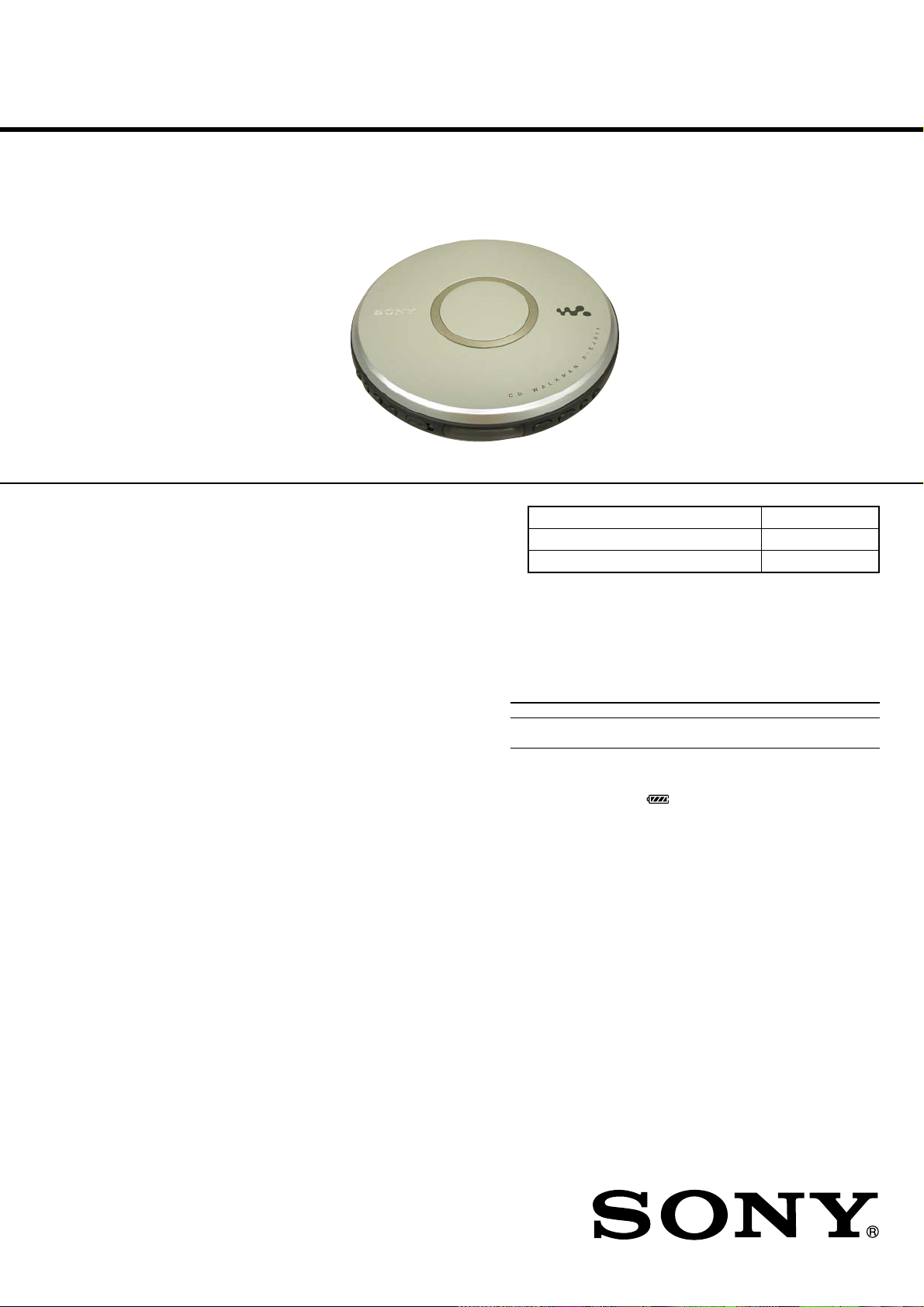
D-EJ011
SERVICE MANUAL
Ver. 1.0 2006.12
SPECIFICATIONS
E Model
Model Name Using Similar Mechanism D-EJ010
CD Mechanism Type CDM-3525A
Optical Pick-up Name DAX-25E
System: Compact disc digital audio system
Laser diode properties
Emission duration: Continuous
Laser output: Less than 44.6 µW (This output is the
value measured at a distance of 200 mm from the
objective lens surface on the optical pick-up block
with 7 mm aperture.)
Power requirements
• Two LR6 (size AA) batteries: 1.5 V DC × 2
Dimensions (w/h/d) (without projecting parts and controls)
Approx. 139.8 × 27.9 × 139.8 mm
Mass (excluding accessories)
Approx.188 g
Operating temperature 5°C - 35°C (41°F - 95°F)
Battery life* (approx. hours)
(When the CD player is used on a flat and stable
place.)
Playing time varies depending on how the CD player
is used.
G-PROTECTION G-on G-off
Two Sony alkaline batteries LR6 (SG)
(produced in Japan)
* Measured value by the standard of JEITA (Japan
Electronics and Information Technology Industries
Association).
• The indicator sections of roughly show the
remaining battery power. One section does not
always indicate one-fourth of the battery power.
Design and specifications are subject to change
without notice.
Supplied accessories
Headphones (1)
16 11
9-887-511-01
2006L02-1
© 2006.12
PORTABLE CD PLAYER
Sony Corporation
Personal Audio Division
Published by Sony Techno Create Corporation

D-EJ011
TABLE OF CONTENTS
1. SERVICING NOTES ................................................ 3
2. GENERAL ................................................................... 3
3. DISASSEMBLY
3-1. Disassembly Flow ........................................................... 4
3-2. Cabinet (Inner) Assy,
Cabinet (Lower) Assy...................................................... 4
3-3. Optical Pick-up (CDM-3525A),
MAIN Board.................................................................... 5
4. ELECTRICAL ADJUSTMENT ............................. 6
5. DIAGRAMS
5-1. Block Diagram ................................................................ 8
5-2. Printed Wiring Board
– Main Board (Side A) – ................................................. 9
5-3. Printed Wiring Board
– Main Board (Side B), Jack Board – ............................. 10
5-4. Schematic Diagram – Main Board (1/2) – ..................... 11
5-5. Schematic Diagram – Main Board (2/2), Jack Board – . 12
5-6. IC Pin Function Description............................................ 15
6. EXPLODED VIEWS ................................................. 17
7. ELECTRICAL PARTS LIST .................................. 18
Notes on chip component replacement
• Never reuse a disconnected chip component.
• Notice that the minus side of a tantalum capacitor may be
damaged by heat.
Flexible Circuit Board Repairing
• Keep the temperature of the soldering iron around 270 ˚C
during repairing.
• Do not touch the soldering iron on the same conductor of the
circuit board (within 3 times).
• Be careful not to apply force on the conductor when soldering
or unsoldering.
CAUTION
Use of controls or adjustments or performance of procedures
other than those specified herein may result in hazardous radiation
exposure.
UNLEADED SOLDER
Boards requiring use of unleaded solder are printed with the leadfree mark (LF) indicating the solder contains no lead.
(Caution: Some printed circuit boards may not come printed with
the lead free mark due to their particular size)
: LEAD FREE MARK
Unleaded solder has the following characteristics.
• Unleaded solder melts at a temperature about 40 °C higher
than ordinary solder.
Ordinary soldering irons can be used but the iron tip has to be
applied to the solder joint for a slightly longer time.
Soldering irons using a temperature regulator should be set to
about 350 °C.
Caution: The printed pattern (copper foil) may peel away if
the heated tip is applied for too long, so be careful!
• Strong viscosity
Unleaded solder is more viscou-s (sticky, less prone to flow)
than ordinary solder so use caution not to let solder bridges
occur such as on IC pins, etc.
• Usable with ordinary solder
It is best to use only unleaded solder but unleaded solder may
also be added to ordinary solder.
SAFETY-RELATED COMPONENT WARNING!!
COMPONENTS IDENTIFIED BY MARK 0 OR DOTTED LINE
WITH MARK 0 ON THE SCHEMATIC DIAGRAMS AND IN
THE PARTS LIST ARE CRITICAL TO SAFE OPERATION.
REPLACE THESE COMPONENTS WITH SONY PARTS WHOSE
PART NUMBERS APPEAR AS SHO WN IN THIS MANUAL OR
IN SUPPLEMENTS PUBLISHED BY SONY.
2
SECTION 1
.
SERVICING NOTES
D-EJ011
NOTES ON HANDLING THE OPTICAL PICK-UP
BLOCK OR BASE UNIT
The laser diode in the optical pick-up block may suffer electrostatic
break-down because of the potential difference generated by the
charged electrostatic load, etc. on clothing and the human body.
During repair, pay attention to electrostatic break-down and also
use the procedure in the printed matter which is included in the
repair parts.
The flexible board is easily damaged and should be handled with
care.
NOTES ON LASER DIODE EMISSION CHECK
The laser beam on this model is concentrated so as to be focused on
the disc reflective surface by the objective lens in the optical pickup block. Therefore, when checking the laser diode emission,
observe from more than 30 cm away from the objective lens.
LASER DIODE AND FOCUS SEARCH OPERATION
CHECK
During normal operation of the equipment, emission of the laser
diode is prohibited unless the upper lid is closed while turning ON
the S811. (push switch type)
The following checking method for the laser diode is operable.
• Method:
Emission of the laser diode is visually checked.
1. Open the upper lid.
2. With a disc not set, turn on the S811 with a screwdriver having
a thin tip as shown in Fig.1.
3. Press the u button.
4. Observing the objective lens, check that the laser diode emits
light.
When the laser diode does not emit light, automatic power
control circuit or optical pick-up is faulty.
In this operation, the objective lens will move up and down 2
times along with inward motion for the focus search.
S811
LOCA TING THE CONTROLS
SOUND/AVLS
2 (headphones) jack
Headphones
P MODE/
VOL –/+*
OPEN
HOLD (rear)
Play mode
SECTION 2
GENERAL
Display
Fig. 1 Method to push the S811
This section is extracted from
instruction manual.
DC IN 4.5 V
=+/
^*(play/pause)
p(stop)
Remaining battery power
Track number
Playing time
Sound mode
Bookmark
* The button has a tactile dot
3
D-EJ011
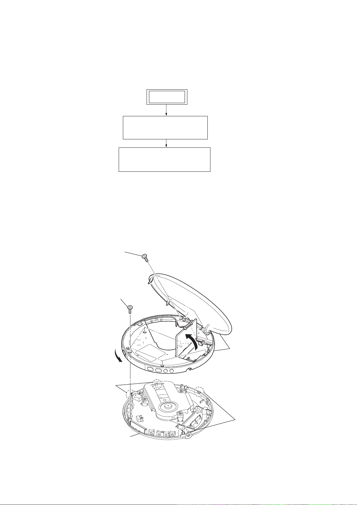
y
• This set can be disassembled in the order shown below.
3-1. DISASSEMBLY FLOW
3-2. CABINET (INNER) ASSY,
CABINET (LOWER) ASSY
3-3. OPTICAL PICK-UP (CDM-3525A),
MAIN BOARD
(Page 5)
SECTION 3
DISASSEMBLY
SET
(Page 4)
Note: Follow the disassembly procedure in the numerical order given.
3-2. CABINET (INNER) ASSY, CABINET (LOWER) ASSY
4
two screws
3
five screws
1
2
cabinet (inner) ass
5
two claws
6
two claws
cabinet (lower) assy
4
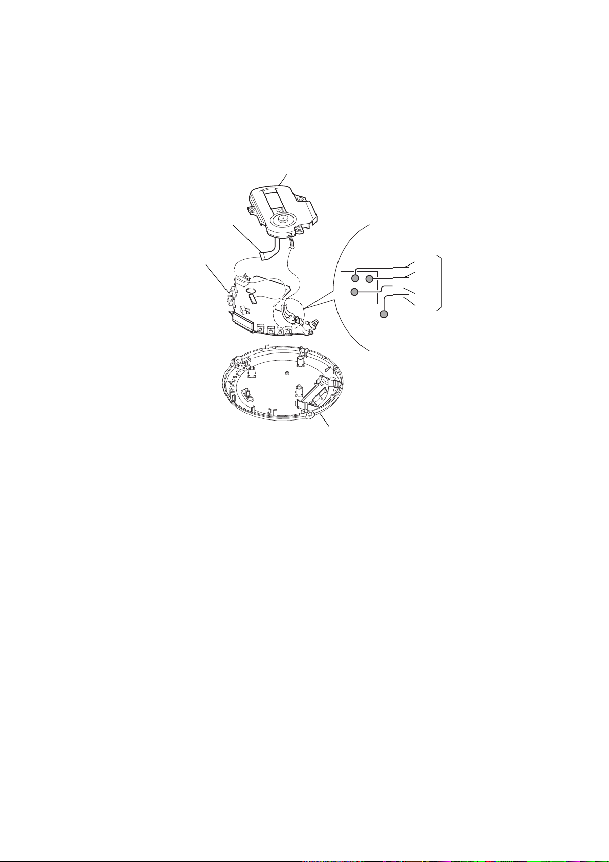
3-3. OPTICAL PICK-UP (CDM-3525A), MAIN BOARD
e
3
optical pick-up CDM-3525A
1
CN501
4
MAIN board
2
Unsolder four lead wires
BLK
RED
ORG
GRY
D-EJ011
To/From
Optical devic
CDM-3525A
MAIN Board (side A)
cabinet (lower) assy
5
D-EJ011
)
SECTION 4
ELECTRICAL ADJUSTMENTS
The CD section adjustments are done automatically in this set.
Adjusting Procedure:
1. Perform check in the order given.
2. Use YEDS-18 disc (Part No: 3-702-101-01) unless otherwise
indicated.
3. Power supply voltage requirement :DC4.5 V in DC IN jack.
(J401)
VOLUME button : Minimum
HOLD switch :OFF
Focus bias Check
Condition:
• Hold the set in horizontal state.
Connection:
MAIN BOARD
X601
R618
R625
R622
(SIDE B)
E
Q602
25
C625
R626
26 50
IC602
(EQOUT)
C627
1
R107
R207
R305
TP604
C110
R101
L301
oscilloscope
(AC range)
SL801
(OPEN)
SL801
(OPEN)
C803
L101
R111
+
–
S811
(OPEN)
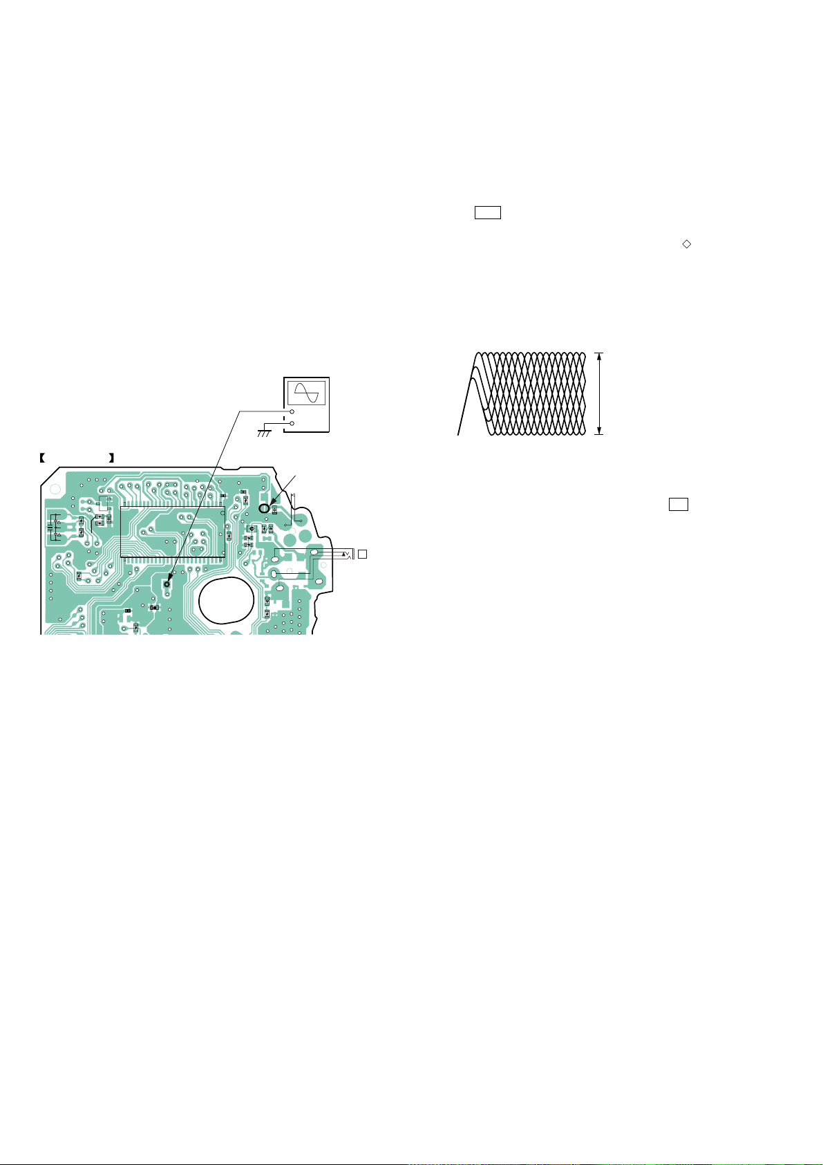
Procedure:
1. Make a solder bridge to short SL801 (OPEN) on the MAIN
board side B.
2. Connect the oscilloscope to the test point TP604 (EQOUT)
and TP406 (M-GND) on the MAIN board side B.
3. Set a disc. (YEDS-18)
4. Press the u button.
5. Check the oscilloscope waveform is as shown below.
A good eye pattern means that the diamond shape ( ) in the
center of the waveform can be clearly distinguished.
RF Signal reference Waveform (Eye Pattern)
VOLT/DIV : 500 mV (With the 10 : 1 probe in use
TIME/DIV : 500ns
RF level
±
0.2 Vp-p
1.3
To watch the eye pattern, set the oscilloscope to AC range and
increase the vertical sensitivity of the oscilloscope for easy
watch-ing.
6. Stop revolving of the disc motor by pressing the x button.
7. SL801 is opened by taking the solder bridge.
1
J30
i
R617
C612
R602
C629
TP604
EQ OUT
L201R211
6