

SONY DCR-TRV410, DCR-TRV410X Service Manual
DCR-TRV410/TRV410E/
TRV510/TRV510E
RMT-814
US Model
SERVICE MANUAL
Ver 1.0 1999.03
Photo: DCR-TRV510
NTSC MODEL : DCR-TRV410/TRV510
PAL MODEL : DCR-TRV410E/TRV510E
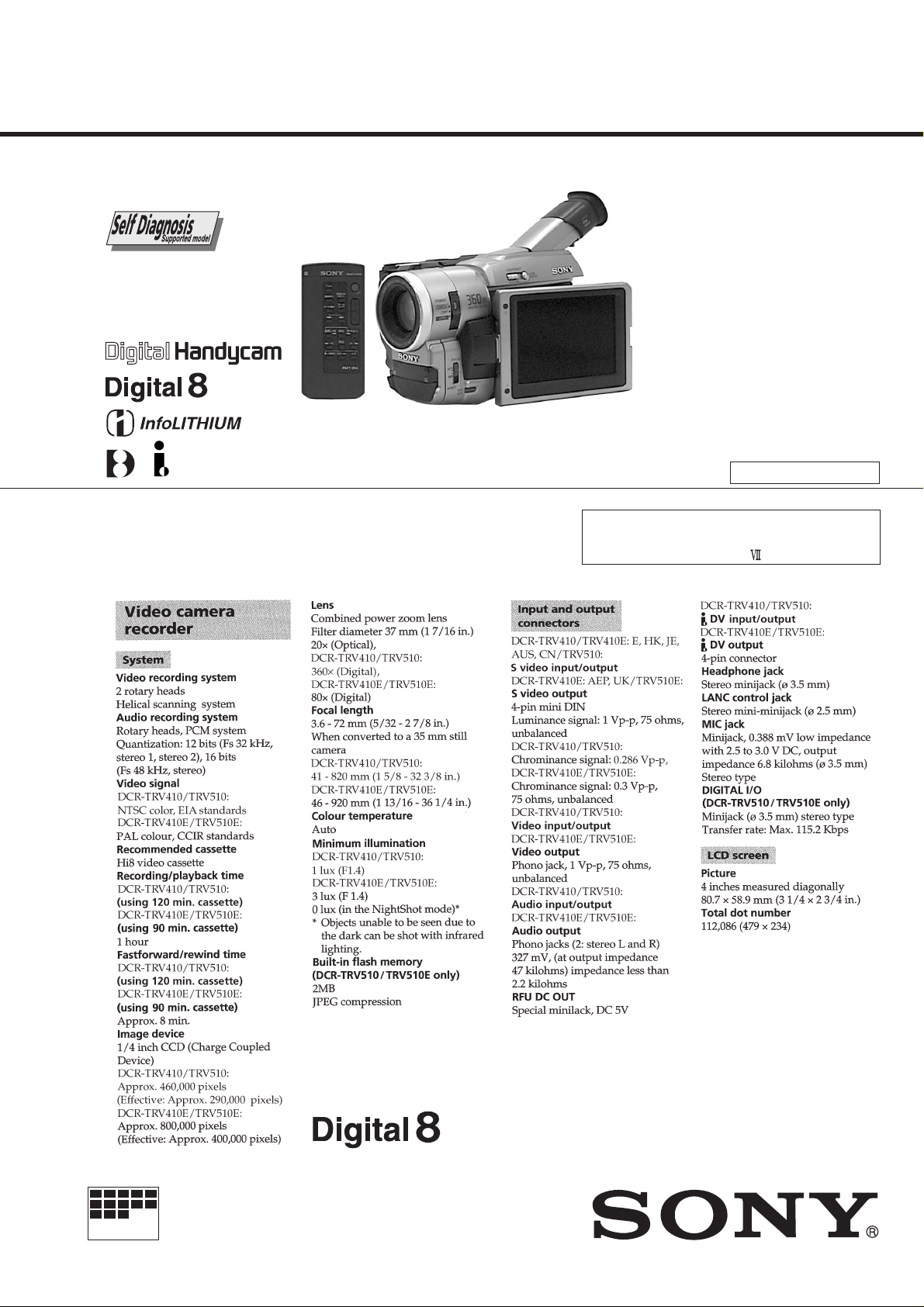
SPECIFICATIONS
Canadian Model
DCR-TRV510
AEP Model
UK Model
DCR-TRV410E/TRV510E
E Model
Hong Kong Model
Tourist Model
DCR-TRV410/TRV410E
Australian Model
Chinese Model
DCR-TRV410E
B800 MECHANISM
For MECHANISM ADJUSTMENT, refer to
the “8mm Video MECHANICAL
ADJUSTMENT MANUAL
” (9-973-801-11).
MICROFILM
• Abbreviation
HK : Hong Kong model
JE : Tourist model
AUS : Australian model
CN : Chinese model
DIGITAL VIDEO CAMERA RECORDER
DCR-TRV410/TRV410E/TRV510/TRV510E
Front of the lens
1.5 m
Pattern box
4-2. PRINTED WIRING BOARDS AND SCHEMATIC DIAGRAMS
THIS NOTE IS COMMON FOR WIRING BOARDS AND SCHEMATIC DIAGRAMS
(In addition to this, the necessary note is printed in each block)
(For printed wiring boards)
• b: Pattern from the side which enables seeing.
(The other layers' patterns are not indicated.)
• Through hole is omitted.
• Circled numbers refer to waveforms.
• There are few cases that the part printed on diagram
isn’t mounted in this model.
• Chip parts.
Transistor Diode
C
5
BE
64
2
13
5
46
2
31
45
2
31
12
4
53
3
21321321
(For schematic diagrams)
• All capacitors are in µF unless otherwise noted. pF : µµF.
50V or less are not indicated except for electrolytics and
tantalums.
• Chip resistors are 1/10W unless otherwise noted.
kΩ=1000Ω, MΩ=1000kΩ.
• Caution when replacing chip parts.
New parts must be attached after removal of chip.
Be careful not to heat the minus side of tantalum capacitor, Because it is damaged by the heat.
• Some chip part will be indicated as follows.
Example C541 L452
22U 10UH
TA A 2520
Kinds of capacitor
Temperature characteristics
External dimensions (mm)
• Constants of resistors, capacitors, ICs and etc with XX indicate
that they are not used.
In such cases, the unused circuits may be indicated.
• Parts with ★ differ according to the model/destination.
Refer to the mount table for each function.
• All variable and adjustable resistors hav e characteristic curve B,
unless otherwise noted.
• Signal name
XEDIT→ EDIT PB/XREC → PB/REC
• 2 : non flammable resistor
• 1 : fusible resistor
• C : panel designation
• A : B+ Line
• B : B– Line
• J : IN/OUT direction of (+,–) B LINE.
• C : adjustment for repair.
• Circled numbers refer to wav eforms.
Note :
The components identified by
mark ! or dotted line with mark
! are critical for safety.
Replace only with part number
specified.
Note :
Les composants identifiés par
une marque ! sont critiques
pour la sécurité.
Ne les remplacer que par une
pièce portant le numéro spécifié.
(Measuring conditions voltage and waveform)
• Voltages and waveforms are measured between the measurement points and ground when camera shoots color bar chart of
pattern box. They are reference values and reference waveforms.
(VOM of DC 10 MΩ input impedance is used.).
• Voltage v alues change depending upon input impedance of V OM
used.)
1. Connection
2. Adjust the distance so that the output waveform of Fig. a and
the Fig. b can be obtain.
Yellow
Cyan
AABBA=B
Fig. a (Video output terminal output waveform)
Cyan
White
Green
Yellow
Fig.b (Picture on monitor TV)
When indicating parts by reference number, pleas include
the board name.
H
White
Green
Red
Magenta
Magenta
Red
Blue
Blue
Electron beam
scanned frame
CRT picture frame
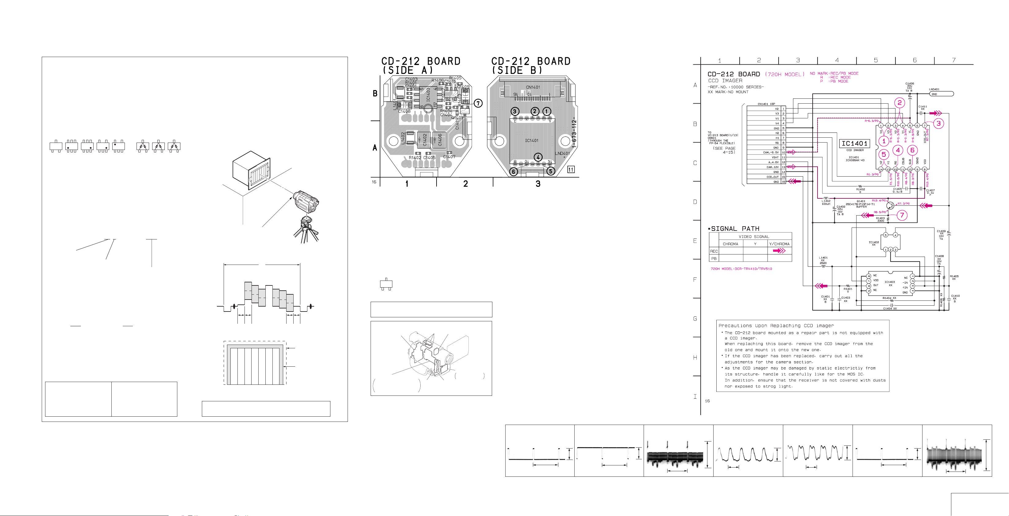
CD-212 (CCD IMAGER) PRINTED WIRING BOARD (720H MODEL)
— Ref. No. CD-212 Board; 10,000 Series —
For printed wiring boards
• This board is eight-layer print board. Howe ver , the patterns of layers two to sev en hav e not been included in
the diagram.
• Chip parts
Transistor
C
BE
There are few cases that the part printed on this
diagram isn’t mounted in this model.
DD-117
(DC/DC CONVERTER)
PC-72 (TRV510/TRV510E)
HONEY, JPEG
D/D CONV, INTERFACE
FLASH MEMORY,
DIGITAL STILL CONTROLLER
VF-126
(COLOR EVF)
PJ-97
(AV IN/OUT)
CD-212 (TRV410/TRV510)
CD-213 (TRV410E/TRV510E)
(CCD IMAGER)
MA-356
STEREO MIC AMP,
LASER LINK
SE-88
(STEADY SHOT)
CD-212
CAMERA REC
BOARD
CD-212 BOARD
C1401 B-1
C1402 A-1
C1403 B-1
C1404 B-2
C1405 A-1
C1406 A-1
C1407 A-2
C1408 B-1
C1409 B-2
C1410 B-2
C1411 B-2
CN1401 B-3
IC1401 A-3
IC1402 B-2
IC1403 B-1
L1401 B-1
L1402 A-1
Q1401 B-2
R1401 B-1
R1402 A-1
R1403 B-2
R1404 B-2
R1405 B-2
R1406 B-2
R1408 B-2
1 IC1401 1,2
2 IC1401 3,4
6.5Vp-p
H
H
3 IC1401 7
6.5Vp-p
H
1.2Vp-p
4 IC1401 !™
5 IC1401 !£,!¢
3.3Vp-p
74 nsec 74 nsec
3.7Vp-p
4-9 4-10 4-11
6 IC1401 0
7 Q1401 E
18Vp-p
H
H
1.3Vp-p
CCD IMAGER
CD-212

DCR-TRV410/TRV410E/TRV510/TRV510E
DCR-TRV410/TRV410E/TRV510/TRV510E
CD-213 (CCD IMAGER) PRINTED WIRING BOARD (960H MODEL)
— Ref. No. CD-213 Board; 10,000 Series —
CD-213 BOARD
C2401 B-1
C2402 A-1
C2403 B-1
C2404 B-2
C2406 A-1
C2407 A-1
C2408 B-1
C2409 A-2
C2410 B-2
C2411 A-2
CN2401 B-3
IC2401 A-3
IC2402 B-2
IC2403 B-2
L2401 B-1
L2402 B-1
Q2401 A-1
R2401 B-2
R2402 A-1
R2403 B-2
R2404 B-2
R2405 B-2
R2406 B-2
For printed wiring boards
• This board is eight-layer print board. Howe ver , the patterns of layers two to sev en hav e not been included in
the diagram.
• Chip parts
Transistor
C
BE
There are few cases that the part printed on this
diagram isn’t mounted in this model.
DD-117
(DC/DC CONVERTER)
PC-72 (TRV510/TRV510E)
HONEY, JPEG
D/D CONV, INTERFACE
FLASH MEMORY,
DIGITAL STILL CONTROLLER
VF-126
(COLOR EVF)
PJ-97
(AV IN/OUT)
CD-212 (TRV410/TRV510)
CD-213 (TRV410E/TRV510E)
(CCD IMAGER)
MA-356
STEREO MIC AMP,
LASER LINK
SE-88
(STEADY SHOT)
CCD IMAGER
CD-213
CD-213
BOARD
CAMERA REC
1 IC2401 1,2
2 IC2401 3,4
6.5Vp-p
H
H
3 IC2401 8
6.5Vp-p
H
0.9Vp-p
4 IC2401 !º
56 nsec
5 IC2401 !¡,!™
3.0Vp-p
56 nsec
4-13 4-14
3.0Vp-p
6 IC2401 !£
7 IC2402 1
18Vp-p
H
H
1.0Vp-p
For schematic diagram
• Refer to page 4-65 for printed wiring board.
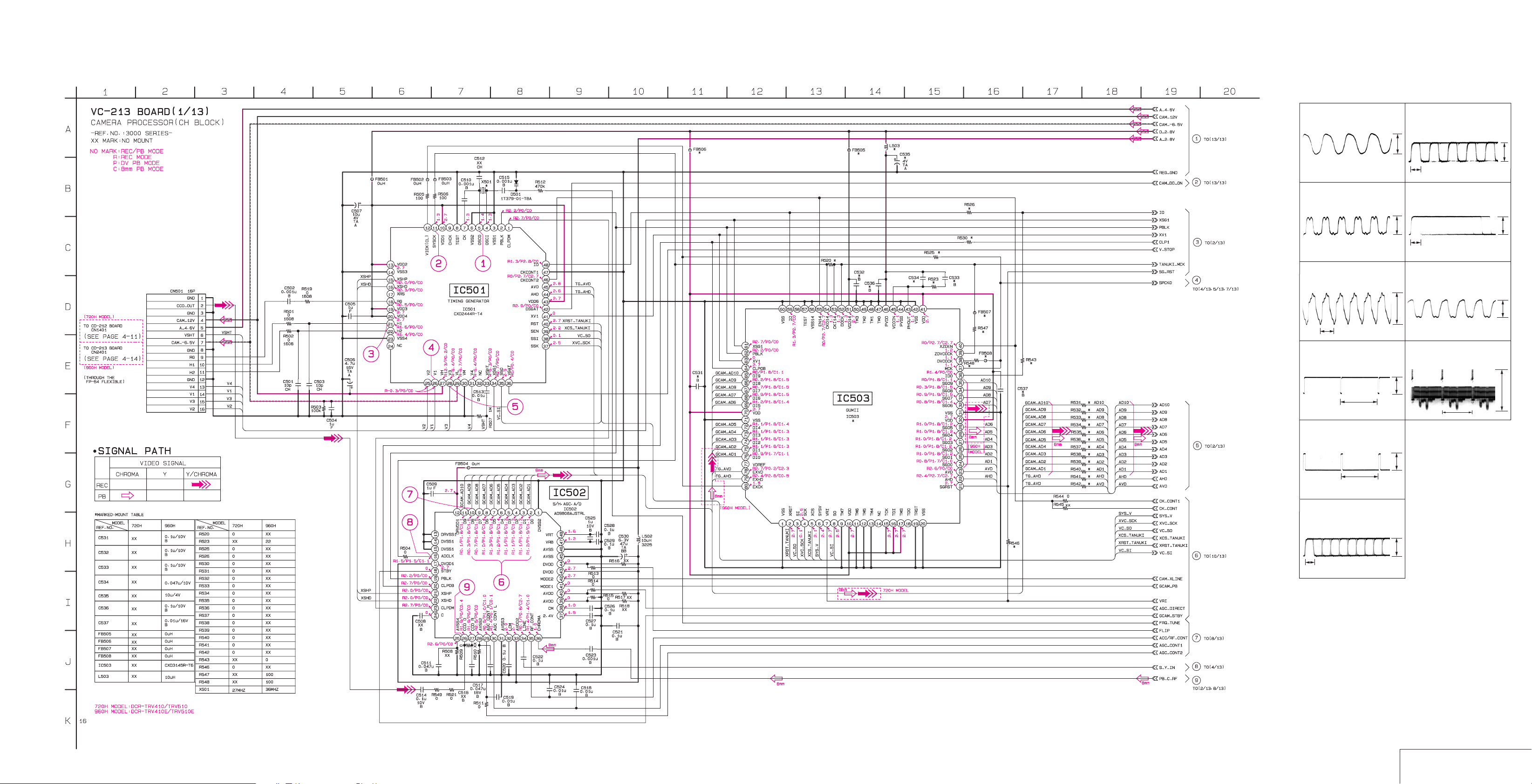
DCR-TRV410/TRV410E/TRV510/TRV510E
VC-213
1
CAMERA REC/PB
2
CAMERA REC/PB
3
CAMERA REC
4
CAMERA REC
IC501 5
NTSC: 27.00 MHz
PAL: 36.00 MHz
IC501 !¡
NTSC: 13.5 MHz
PAL: 18.00 MHz
IC501 @¡
NTSC: 74 nsec
PAL: 56 nsec
IC501 @§
BOARD (1/13)
7
IC502 !º
CAMERA REC
3.0Vp-p
7
IC502 !º PB
3.0Vp-p
8
IC502 !§
CAMERA REC/PB
LINE REC
3.0Vp-p
9
IC502 @§
CAMERA REC
NTSC:74 nsec
PAL:56 nsec
NTSC: 74 nsec
PAL: 56 nsec
NTSC: 13.50 MHz
PAL: 18.00 MHz
2.9Vp-p
NTSC: 1.2Vp-p
PAL: 0.9Vp-p
2.9Vp-p
2.9Vp-p
H
5
IC501 @•
CAMERA REC
H
6
IC502 2 – 9
CAMERA REC/PB
NTSC: 74 nsec
PAL: 56 nsec
7.0Vp-p
H
7.0Vp-p
2.9Vp-p
4-15 4-16 4-17
CAMERA PROCESSOR
VC-213 (1/13)
DCR-TRV410/TRV410E/TRV510/TRV510E
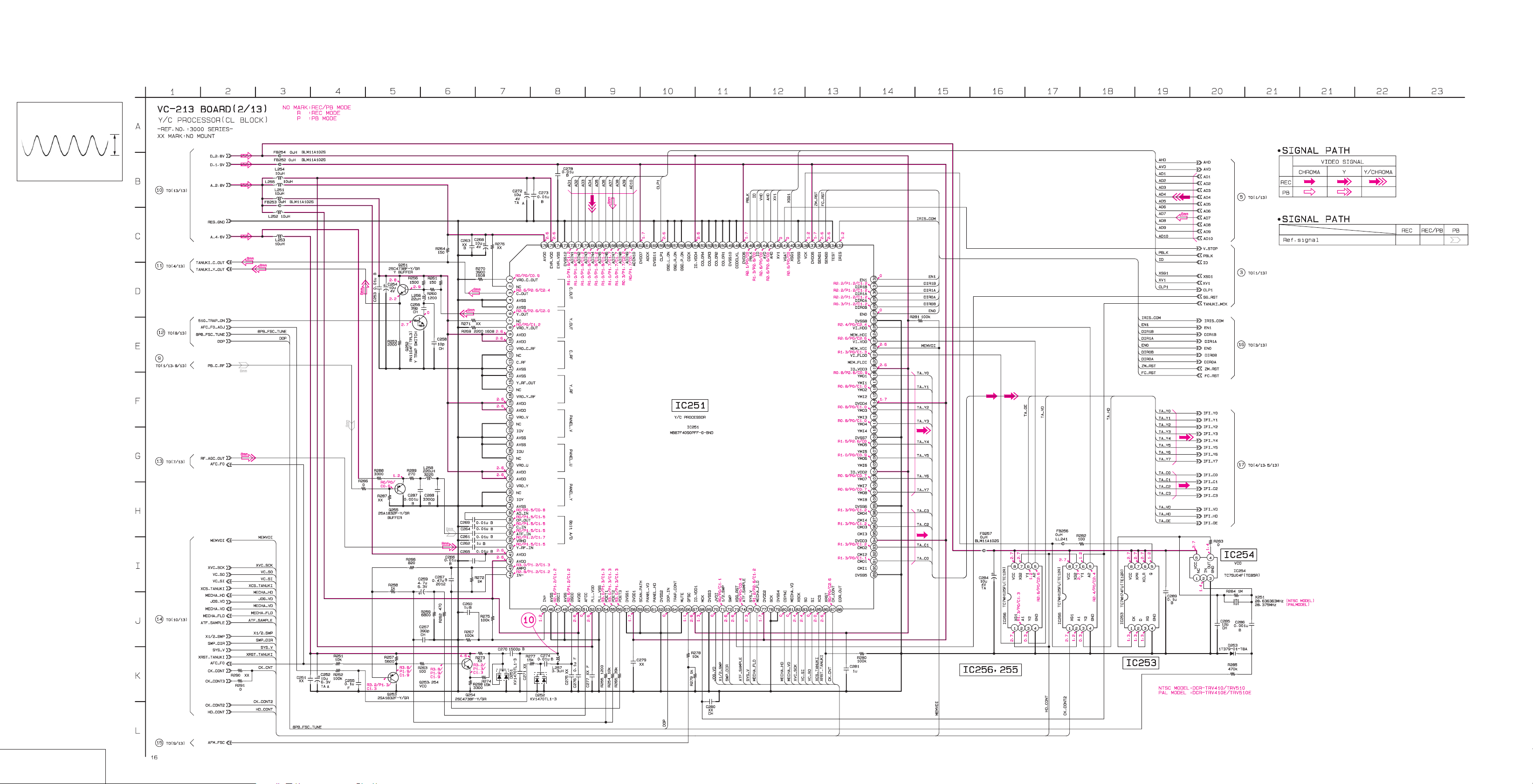
For schematic diagram
• Refer to page 4-65 for printed wiring board.
VC-213
0
LINE REC/PB
BOARD (2/13)
IC251 $¶, L257
NTSC :13.3 MHz
PAL : 13.6 MHz
3.0Vp-p
Y/C PROCESSOR
VC-213 (2/13)
4-18 4-19 4-20

For schematic diagram
• Refer to page 4-65 for printed wiring board.
DCR-TRV410/TRV410E/TRV510/TRV510E
DCR-TRV410/TRV410E/TRV510/TRV510E
4-21 4-22
LENS MOTOR DRIVE
VC-213 (3/13)
DCR-TRV410/TRV410E/TRV510/TRV510E
For schematic diagram
• Refer to page 4-65 for printed wiring board.
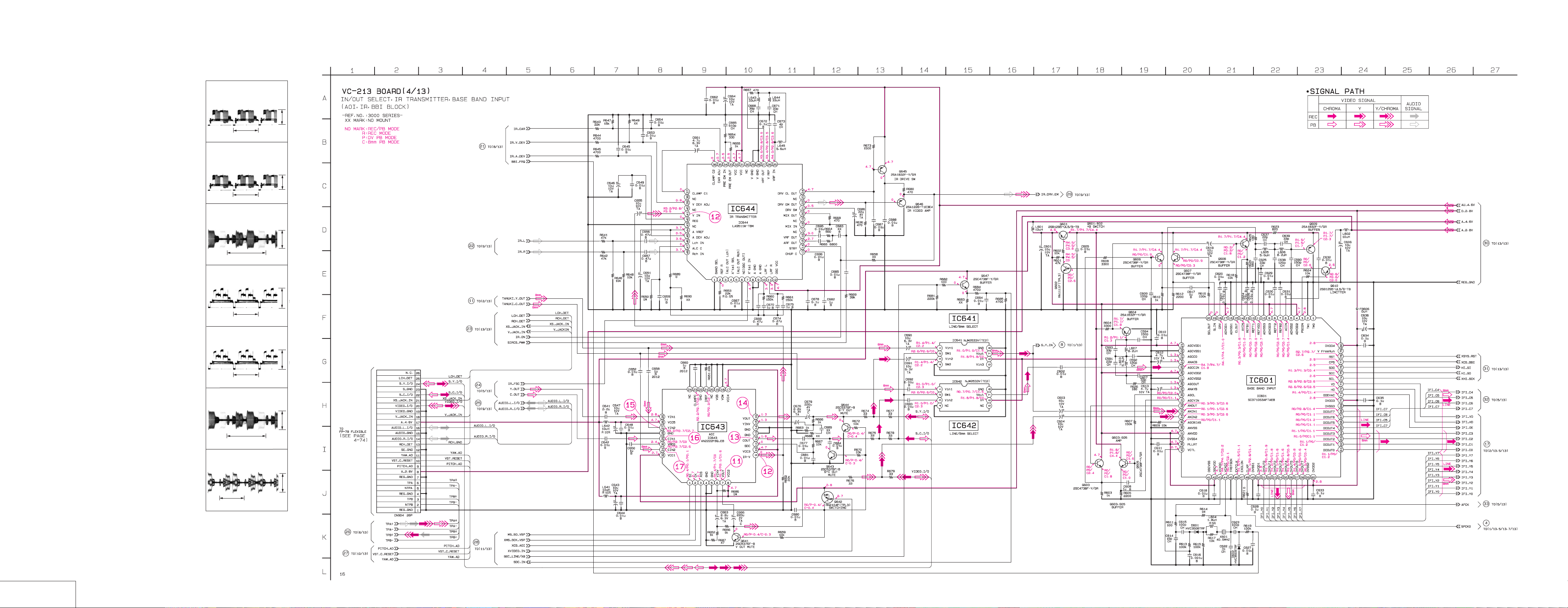
VC-213 BOARD (4/13)
!¡ IC643 7
CAMERA REC/PB
H
!™ IC643 9, IC644 $¡
CAMERA REC/PB
IR ON
H
!£ IC643 !™
CAMERA REC/PB
H
!¢ IC643 !§
CAMERA REC/PB
H
!∞ IC643 @¶ PB
2Vp-p
0.5Vp-p
1.0Vp-p
1.5Vp-p
H
!§ IC643 @ª PB
H
!¶ IC643 #¡ PB
H
0.5Vp-p
0.3Vp-p
0.5Vp-p
I/O SEL, IR, BBI
VC-213 (4/13)
4-26 4-274-25
4-28
For schematic diagram
• Refer to page 4-65 for printed wiring board.
DCR-TRV410/TRV410E/TRV510/TRV510E
VC-213
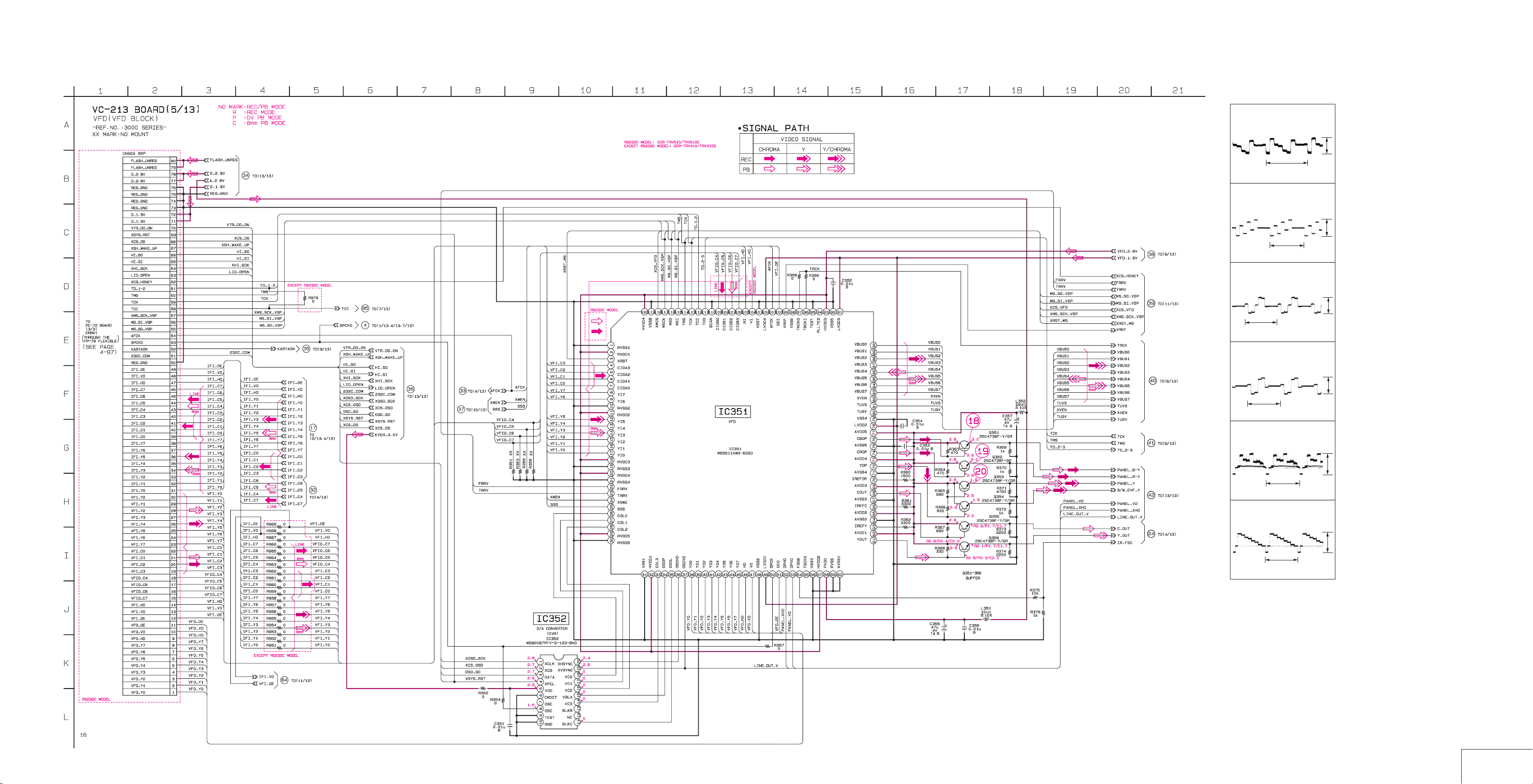
!•
CAMERA REC/PB
!•
LINE REC
!ª
CAMERA REC/PB
!ª
LINE REC
BOARD (5/13)
Q351 E
H
Q351 E
H
Q352 E
H
Q352 E
0.15Vp-p
0.4Vp-p
0.4Vp-p
H
@º
Q353 E
CAMERA REC/PB
H
@º
Q353 E
LINE REC
H
0.4Vp-p
0.4Vp-p
0.4Vp-p
4-29 4-30
4-31
VFD
VC-213 (5/13)
DCR-TRV410/TRV410E/TRV510/TRV510E
DCR-TRV410/TRV410E/TRV510/TRV510E
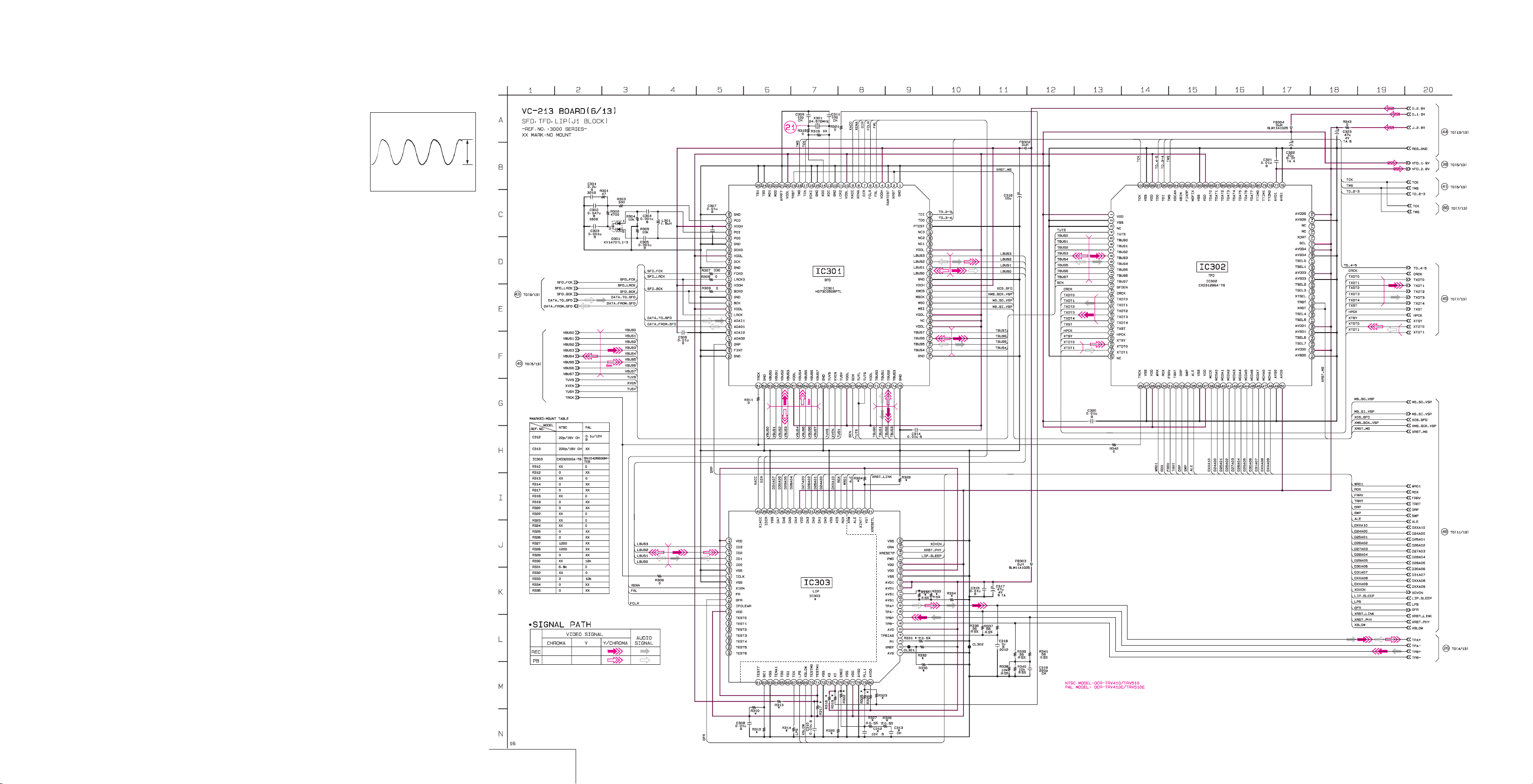
For schematic diagram
• Refer to page 4-65 for printed wiring board.
VC-213
CAMERA REC/PB
@¡
BOARD (6/13)
IC301 !¢ (R315)
24.58MHz
2.6Vp-p
SFD, TFD, LIP
VC-213 (6/13)
4-33 4-344-32
 Loading...