

Sony DCR-PC109E, DCR-PC109 Service Manual
DCR-PC109/PC109E
RMT-831
SERVICE MANUAL
Ver 1.0 2004. 01
Revision History
Revision History
How to use
How to use
Acrobat Reader
Acrobat Reader
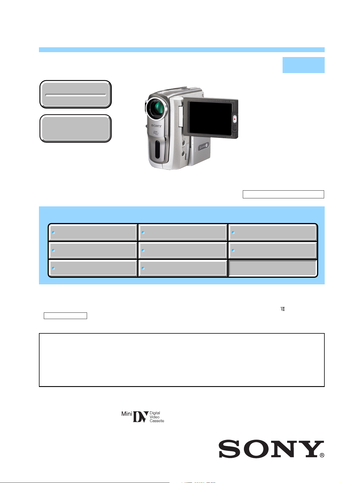
Photo : DCR-PC109
Link
Link
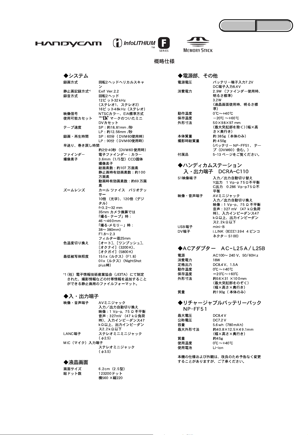
SPECIFICATIONS
SPECIFICATIONS
BLOCK DIAGRAMS
BLOCK DIAGRAMS
LEVEL 2
DCR-PC109
US Model
Canadian Model
Japanese Model
Korea Model
DCR-PC109E
AEP Model
UK Model
North European Model
Australian Model
Chinese Model
DCR-PC109/PC109E
E Model
Hong Kong Model
Tourist Model
Z MECHANISM (MDX-Z200)
PRINTED WIRING BOARDS
PRINTED WIRING BOARDS
SERVICE NOTE
SERVICE NOTE
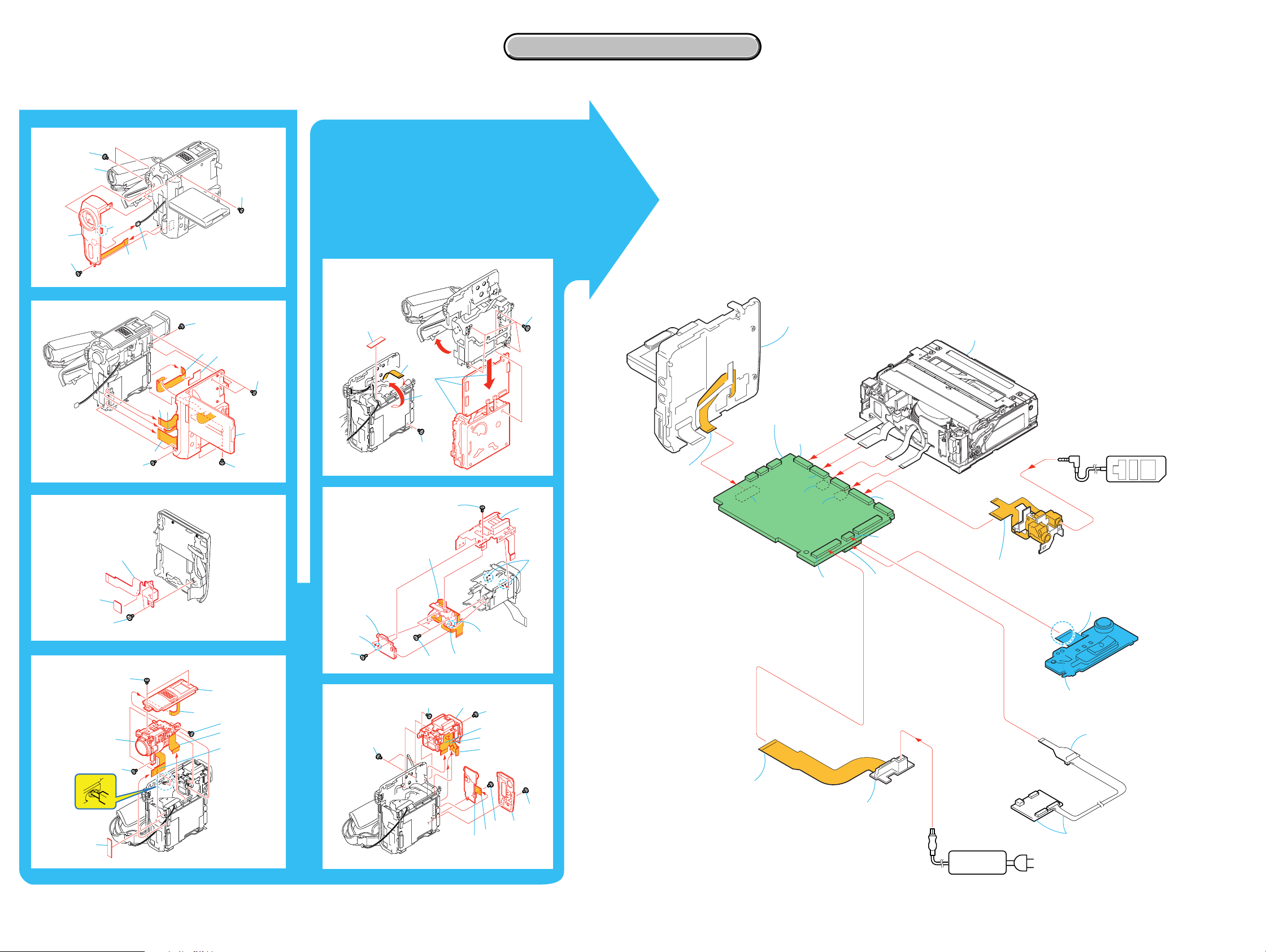
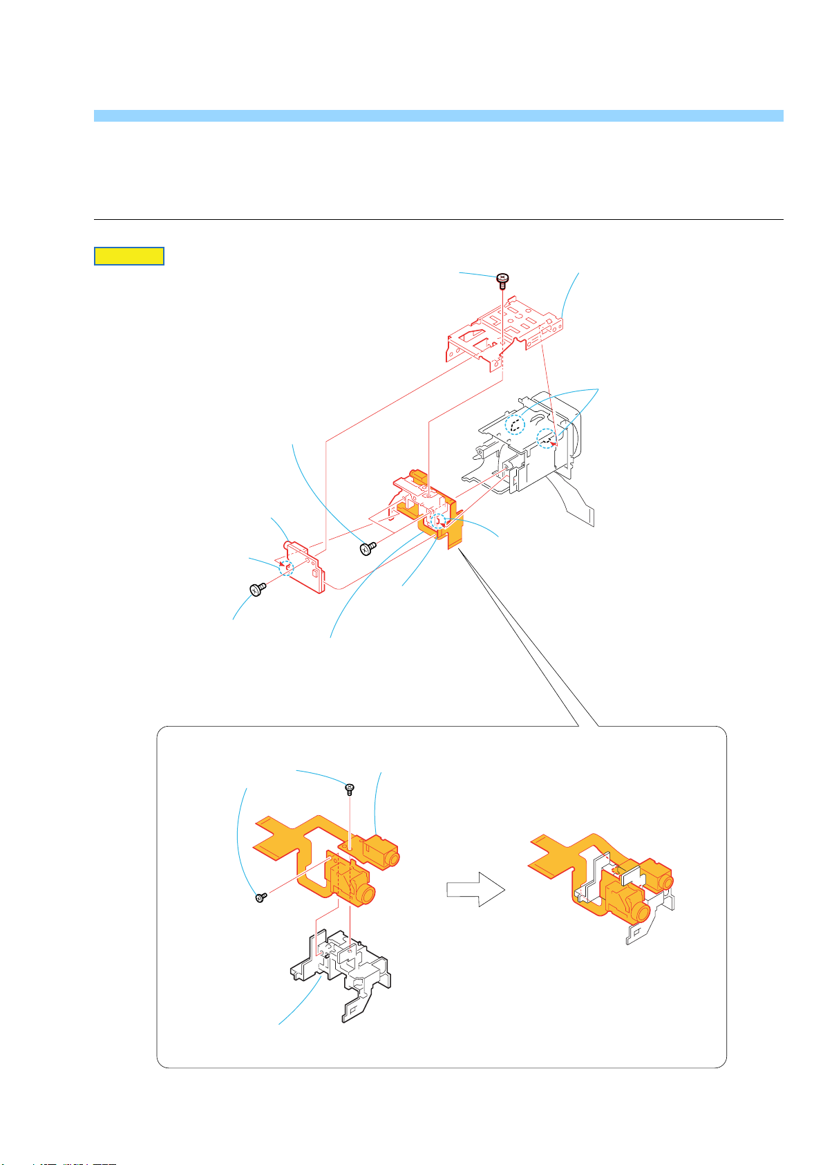
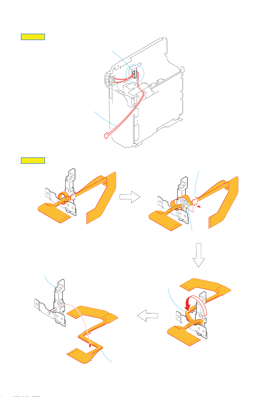
DISASSEMBLY
DISASSEMBLY
• For ADJUSTMENTS (SECTION 6), refer to SERVICE MANUAL, ADJ (987670651.pdf).
• For INSTRUCTION MANUAL, refer to SERVICE MANUAL, LEVEL 1 (987670641.pdf). (EXCEPT J MODEL)
• For MECHANISM ADJUSTMENTS, refer to the “DV MECHANICAL ADJUSTMENT MANUAL
Z MECHANISM ” (EXCEPT J: 9-876-210-11) (J: 9-876-210-01).
• Reference number search on printed wiring boards is available.
On the VC-352 board
This service manual provides the information that is premised the circuit board replacement service and not intended repair
inside the VC-352 board.
Therefore, schematic diagram, printed wiring board, mounted parts location and electrical parts list of the VC-352 board are not
shown.
The following pages are not shown.
Schematic diagram .............................Pages 4-23 to 4-64
Printed wiring board ............................Pages 4-79 to 4-82
FRAME SCHEMATIC DIAGRAMS
FRAME SCHEMATIC DIAGRAMS
SCHEMATIC DIAGRAMS
SCHEMATIC DIAGRAMS
Mounted parts location .............................
Electrical parts list ................................... Pages 5-17 to 5-25
REPAIR PARTS LIST
REPAIR PARTS LIST
Pages 4-87 to 4-88
DIGITAL VIDEO CAMERA RECORDER

Video camera recorder
System
Video recordin g s ys t em
2 rotary he ads, Helical scanning system
Still image reco rd in g sy s t em
Exif Ver. 2.2 *1
*1 “Exif” is a file format for still images,
established by the JEITA (J ap an El ectronics
and Information Technology Industries
Association). Files in this format can have
additional information such as your
camcorder’s setting information at the time of
recording.
Audio recordi n g system
Rotary heads, PCM system
Quantization: 12 bits (Fs 32 kHz, stereo 1,
stereo 2), 16 bits (Fs 48 kHz, stereo)
Video signal
DCR-PC109: NTSC color, EIA standards
DCR-PC109E: PAL color, CCIR standards
Usable cassette
Mini DV cassette with the mark
printed
Tape speed
SP: Approx. 18.81 mm/s
LP: Approx. 12.56 mm/s
Recording/playback time (using a DVM60
cassette)
SP: 60 min
LP: 90 min
Fast forward/rewind time (using a DVM60
cassette)
Approx. 2 min 40 s
Viewfinder
Electric viewfinder (color)
Image device
3.6 mm (1/5 type) CC D (Charge Coupled
Device)
Gross: Approx. 1 070 000 pixels
Effective (still): Approx. 1 000 000 pixels
Effective (mov ie): Approx. 690 000 pixels
Lens
Carl Zeiss Vario-Tessar
Combined power zoom lens
Filter diameter: 25 mm (1 1/2 in.)
10× (Opt ical), 120× (Digital)
F = 1.8 ~ 2.3
Focal length
3.2 - 32 mm (5/32 - 1 5/16 i n. )
When converted to a 35 mm still camera
In CAMERA-TA P E:
46 - 460 mm (1 13/16 - 18 1/8 in.)
In CAMERA-MEM:
38 - 380 mm (1 1/2 - 15 in.)
Color temperature
[AUTO], [ONE PUSH], [INDOOR] (3 200
K), [OUTDOOR] (5 800 K)
Minimum illumination
7 1x (lux) (F 1.8)
0 lx (lux) (during NightShot plu s func ti on)*
* Objects unable to be seen due to the dark can be
shot with infrared lighting.
SPECIFICATIONS
Input/Output connectors
Audio/Video input/output
AV MINIJACK
Video signal: 1 V p- p, 75 Ω (ohms),
unbalanced, sync nega ti ve
Audio signal: 327 mV (at ou tput impedance
more than 47 kΩ (kilohms)), Input impedance
more than 47 kΩ(kilohms), Output impe dance
with less than 2.2 kΩ (kilohms)
LANC jack
Stereo mini-minijack (Ø 2.5 m m )
MIC jack
Minijack, 0.388 mV low impe da nc e w i th DC
2.5 to 3.0 V, output impedance 6.8 kΩ
(kilohms) (Ø 3.5 mm), Stereo type
LCD screen
Picture
6.2 cm (2.5 type)
Total dot number
123 200 (560 × 220)
General
Power requirements
DC 7.2 V (battery pack)
DC 8.4 V (AC Adaptor)
Average power consumption (when using the
battery pack)
During camera recording using the viewfinder
2.9 W
During camera recording using the LCD
3.2 W
Operating temperature
0°C to 40°C (32°F to 104°F)
Storage temperature
-20°C to + 60°C (-4°F to + 140°F)
Dimensions (approx.)
50 × 98 × 97 mm (2 × 37/8 × 37/8 in.)
(w/h/d)
Mass (approx.)
385 g (13 oz) main unit only
450 g (15 oz) including the NP-FF51
rechargeable ba tt ery pack and DVM60
cassette.
Supplied accessories
See page 5-12.
Handycam Station DCRA-C111
S video input/output
Luminance signal: 1 Vp-p, 75 Ω (ohms),
unbalanced
Chrominance signal:
DCR-PC109: 0.286Vp-p
DCR-PC109E: 0.3Vp-p
75 Ω (ohms), unbalanced
4-pin mini DIN
Audio/Video input/output
AV MINIJACK
Input/output auto switch
Video signal: 1 Vp-p, 75
unbalanced, sync negative
Audio signal: 327 mV, (at ou tpu t
impedance more tha n 47 kΩ (kilohm s ))
Input impedance more than 47 kΩ (kilohms)
Output impedance with less than 2.2 kΩ
(kilohms)
Ω (ohms),
DCR-PC109/PC109E
ENGLISH JAPANESE
ENGLISH JAPANESE
USB jack
mini-B
DV input/output
4-pin connector
AC Adaptor AC-L25A/L25B
Power requireme nt s
AC 100 - 240 V, 50/60 Hz
Current consumption
0.35 - 0.18 A
Power consumption
18 W
Output voltage
DC 8.4 V, 1.5 A
Operating temper ature
0°C to 40°C (32°F to 104°F)
Storage temperature
-20°C to + 60°C (-4°F to + 140°F)
Dimensions (approx.)
56 × 31 × 100 mm (2 1/4 × 11/4 × 4 in.)
(w/h/d) excluding the project i ng pa rts
Mass (approx.)
190 g (6.7 oz) excluding the power cord
Rechargeable battery pack (NP-FF51)
Maximum output voltage
DC 8.4 V
Output voltage
DC 7.2 V
Capacity
5.6 Wh (780 mAh)
Dimensions (approx.)
40.8 × 12.5 × 49.1 mm
(1 5/8 × 1/2 × 1 15/16 in.) (w/h /d)
Mass (approx.)
45 g (1.6 oz)
Operating temperature
0°C to 40°C (32°F to 104°F)
Type
Lithium ion
Design and specifications are subject to
change without notice.
— 2 —
DCR-PC109/PC109E
ENGLISH JAPANESE
ENGLISH JAPANESE
— 3 —

SAFETY CHECK-OUT
After correcting the original service problem, perform the following
safety checks before releasing the set to the customer.
DCR-PC109/PC109E
ENGLISH JAPANESE
ENGLISH JAPANESE
1. Check the area of your repair for unsoldered or poorly-soldered
connections. Check the entire board surface for solder splashes
and bridges.
2. Check the interboard wiring to ensure that no wires are
"pinched" or contact high-wattage resistors.
3. Look for unauthorized replacement parts, particularly
transistors, that were installed during a previous repair . Point
them out to the customer and recommend their replacement.
4. Look for parts which, through functioning, show obvious signs
of deterioration. Point them out to the customer and
recommend their replacement.
5. Check the B+ voltage to see it is at the values specified.
6. Flexible Circuit Board Repairing
• Keep the temperature of the soldering iron around 270˚C
during repairing.
• Do not touch the soldering iron on the same conductor of the
circuit board (within 3 times).
• Be careful not to apply force on the conductor when soldering
or unsoldering.
SAFETY-RELATED COMPONENT WARNING!!
COMPONENTS IDENTIFIED BY MARK 0 OR DOTTED LINE WITH
MARK 0 ON THE SCHEMATIC DIAGRAMS AND IN THE PARTS
LIST ARE CRITICAL TO SAFE OPERATION. REPLACE THESE
COMPONENTS WITH SONY PARTS WHOSE PART NUMBERS
APPEAR AS SHOWN IN THIS MANUAL OR IN SUPPLEMENTS
PUBLISHED BY SONY.
Unleaded solder
Boards requiring use of unleaded solder are printed with the leadfree mark (LF) indicating the solder contains no lead.
(Caution: Some printed circuit boards may not come printed with
the lead free mark due to their particular size.)
: LEAD FREE MARK
Unleaded solder has the following characteristics.
• Unleaded solder melts at a temperature about 40°C higher than
ordinary solder.
Ordinary soldering irons can be used but the iron tip has to be
applied to the solder joint for a slightly longer time.
Soldering irons using a temperature regulator should be set to
about 350°C.
Caution: The printed pattern (copper foil) may peel away if the
heated tip is applied for too long, so be careful!
• Strong viscosity
Unleaded solder is more viscous (sticky , less pr one to flo w) than
ordinary solder so use caution not to let solder bridges occur such
as on IC pins, etc.
• Usable with ordinary solder
It is best to use only unleaded solder but unleaded solder may
also be added to ordinary solder.
ATTENTION AU COMPOSANT AYANT RAPPORT
À LA SÉCURITÉ!
LES COMPOSANTS IDENTIFÉS PAR UNE MARQUE 0 SUR LES
DIAGRAMMES SCHÉMATIQUES ET LA LISTE DES PIÈCES SONT
CRITIQUES POUR LA SÉCURITÉ DE FONCTIONNEMENT. NE
REMPLACER CES COMPOSANTS QUE PAR DES PIÈSES SONY
DONT LES NUMÉROS SONT DONNÉS DANS CE MANUEL OU
DANS LES SUPPÉMENTS PUBLIÉS PAR SONY.
CAUTION :
Danger of explosion if battery is incorrectly replaced.
Replace only with the same or equivalent type.
— 4 —
DCR-PC109/PC109E
ENGLISH JAPANESE
ENGLISH JAPANESE
— 5 —

DCR-PC109/PC109E
TABLE OF CONTENTS
1. SERVICE NOTE
1-1. SER VICE NOTE ····························································· 1-1
1. NOTE FOR REPAIR ·······················································1-1
2. POWER SUPPLY DURING REPAIRS ··························1-2
3. TO TAKE OUT A CASSETTE WHEN NOT EJECT
(FORCE EJECT) ·····························································1-2
2. DISASSEMBLY
2-1. DISASSEMBLY······························································2-1
2-2. SERVICE POSITION ·····················································2-3
2-3. CIRCUIT BOARDS LOCATION ···································2-6
2-4. FLEXIBLE BOARDS LOCATION ································2-7
HELP (List of caution points is shown here.)
3. BLOCK DIAGRAMS
3-1. OVERALL BLOCK DIAGRAM (1/4) ···························3-1
3-2. OVERALL BLOCK DIAGRAM (2/4) ···························3-3
3-3. OVERALL BLOCK DIAGRAM (3/4) ···························3-5
3-4. OVERALL BLOCK DIAGRAM (4/4) ···························3-7
3-5. POWER BLOCK DIAGRAM (1/3)································3-9
3-6. POWER BLOCK DIAGRAM (2/3)······························3-11
4. PRINTED WIRING BOARDS AND
SCHEMATIC DIAGRAMS
4-1. FRAME SCHEMATIC DIAGRAM (1/2)······················· 4-1
FRAME SCHEMATIC DIAGRAM (2/2)······················· 4-3
4-2. SCHEMATIC DIAGRAMS
• CD-494 (CCD IMAGER)
SCHEMATIC DIAGRAM ······························4-7
• PD-213 (LCD RGB DRIVE, BACKLIGHT)
SCHEMATIC DIAGRAM ······························4-9
• CONTROL KEY BLOCK (SB6300)
SCHEMATIC DIAGRAM ······························4-9
• LB-096 (EVF RELAY)
SCHEMATIC DIAGRAM ····························4-11
• SE-140 (PITCH/YAW SENSOR AMP, MIC IN)
SCHEMATIC DIAGRAM ····························4-12
• CR-047 (CRADLE CONNECTOR)
SCHEMATIC DIAGRAM ····························4-13
• FP-847 FLEXIBLE
SCHEMATIC DIAGRAM ····························4-14
• FP-840 (SIRCS, FRONT INDICATOR)
SCHEMATIC DIAGRAM ····························4-15
• IR-052 (NIGHT SHOT)
SCHEMATIC DIAGRAM ····························4-15
• MS-201 (MS CONNECTOR)
SCHEMATIC DIAGRAM ····························4-15
• CONTROL SWITCH BLOCK (SS6800, ZM6800)
SCHEMATIC DIAGRAM ····························4-17
• FP-926 (PANEL REVERSE)
SCHEMATIC DIAGRAM ····························4-17
• FP-841 FLEXIBLE (BAT/DC IN)
SCHEMATIC DIAGRAM ····························4-19
• FP-843 FLEXIBLE
SCHEMATIC DIAGRAM ····························4-20
• FP-467/228/826 FLEXIBLE (S/T REEL SENSOR,
TAPE SENSOR)
SCHEMATIC DIAGRAM ····························4-21
4-3. PRINTED WIRING BOARDS
• CD-494 (CCD IMAGER)
PRINTED WIRING BOARD ·······················4-69
• IR-052 (NIGHT SHOT)
PRINTED WIRING BOARD ·······················4-69
• CR-047 (CRADLE CONNECTOR)
PRINTED WIRING BOARD ·······················4-71
• LB-096 (EVF RELAY)
PRINTED WIRING BOARD ·······················4-72
• PD-213 (LCD RGB DRIVE, BACKLIGHT)
PRINTED WIRING BOARD ·······················4-73
• MS-201 (MS CONNECTOR)
PRINTED WIRING BOARD ·······················4-75
• SE-140 (PITCH/YAW SENSOR AMP)
PRINTED WIRING BOARD ·······················4-77
• FP-228/467/826 FLEXIBLE BOARD
(S/T REEL SENSOR, TAPE SENSOR) ·····················4-77
Printed wiring board of the VC-352 board is not shown.
Pages from 4-79 to 4-82 are not shown.
4-4. MOUNTED PARTS LOCATION ·································4-85
Mounted parts location of the VC-352 board is not shown.
Pages from 4-87 to 4-88 are not shown.
5. REPAIR PARTS LIST
5-1. EXPLODED VIEWS ······················································5-3
5-1-1.OVERALL SECTION·····················································5-3
5-1-2.MAIN CHASSIS (LENS) SECTION ·····························5-4
5-1-3.EVF SECTION································································5-5
5-1-4.CABINET (L) SECTION················································ 5-6
5-1-5.CABINET (R) SECTION-1 ············································ 5-7
5-1-6.CABINET (R) SECTION-2 ············································ 5-8
5-1-7.OVERALL (MECHANISM DECK-Z200)·····················5-9
5-1-8.LS CHASSIS BLOCK ASSEMBLY·····························5-10
5-1-9.MECHANISM CHASSIS BLOCK ASSEMBLY········· 5-11
5-2. ELECTRICAL PARTS LIST ········································ 5-14
Electrical parts list of the VC-352 board is not shown.
Pages from 5-17 to 5-25 are not shown.
Shematic diagram of the VC-352 board is not shown.
Pages from 4-23 to 4-64 are not shown.
— 6 —
DCR-PC109/PC109E
SECTION 1
SERVICE NOTE
1-1. SERVICE NOTE
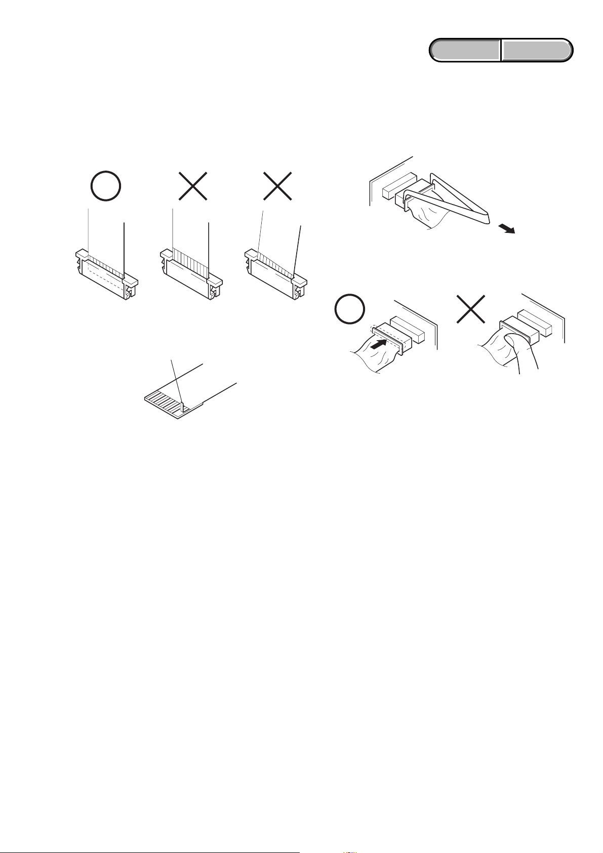
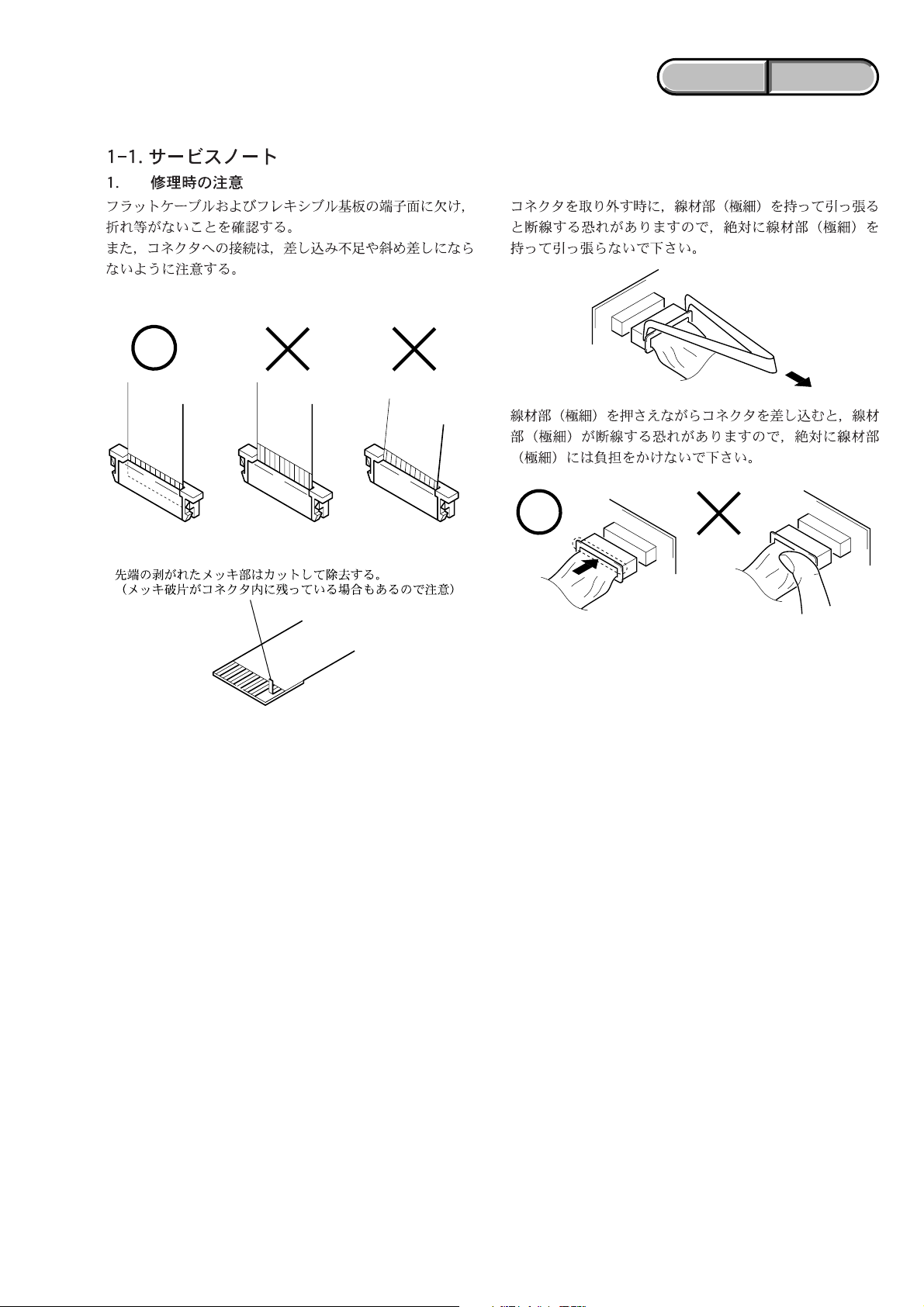
1. NOTE FOR REPAIR
Make sure that the flat cable and flexible board are not cracked of
bent at the terminal.
Do not insert the cable insufficiently nor crookedly.
Cut and remove the part of gilt
which comes off at the point.
(Take care that there are
some pieces of gilt left inside)
ENGLISH JAPANESE
ENGLISH JAPANESE
When remove a connector, don't pull at wire of connector.
Be in danger of the snapping of a wire.
When installing a connector, don't press down at wire of connector.
Be in danger of the snapping of a wire.
1-1
DCR-PC109/PC109E
ENGLISH JAPANESE
ENGLISH JAPANESE
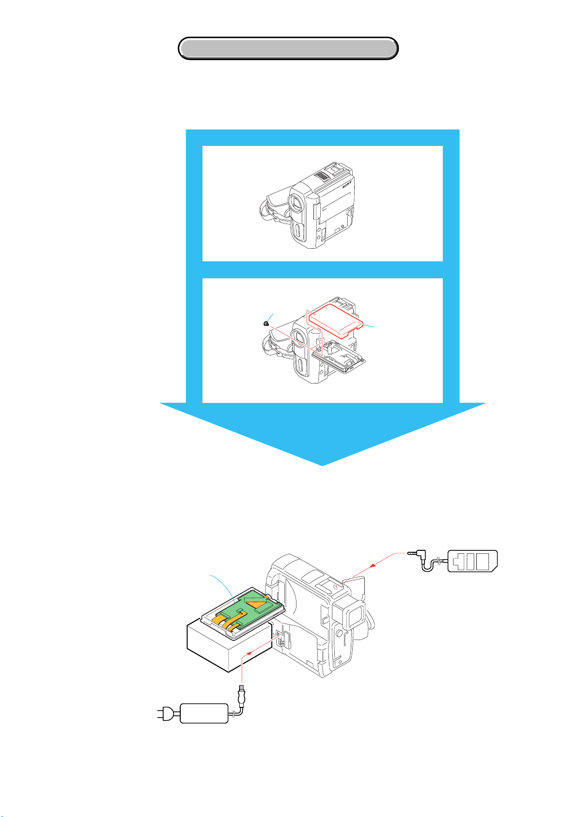
2. POWER SUPPLY DURING REPAIRS
In this unit, about 10 seconds after power is supplied to the battery terminal using the regulated power supply (8.4V), the po wer is shut of f so
that the unit cannot operate.
This following two methods are available to prevent this. Take note of which to use during repairs.
Method 1.
Use the AC power adaptor.
Method 2.
Connect the servicing remote commander RM-95 (J-6082-053-B) to the LANC jack, and set the commander switch to the “ADJ” side.
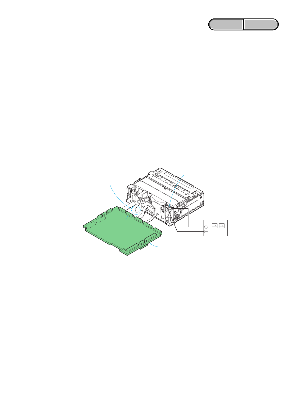
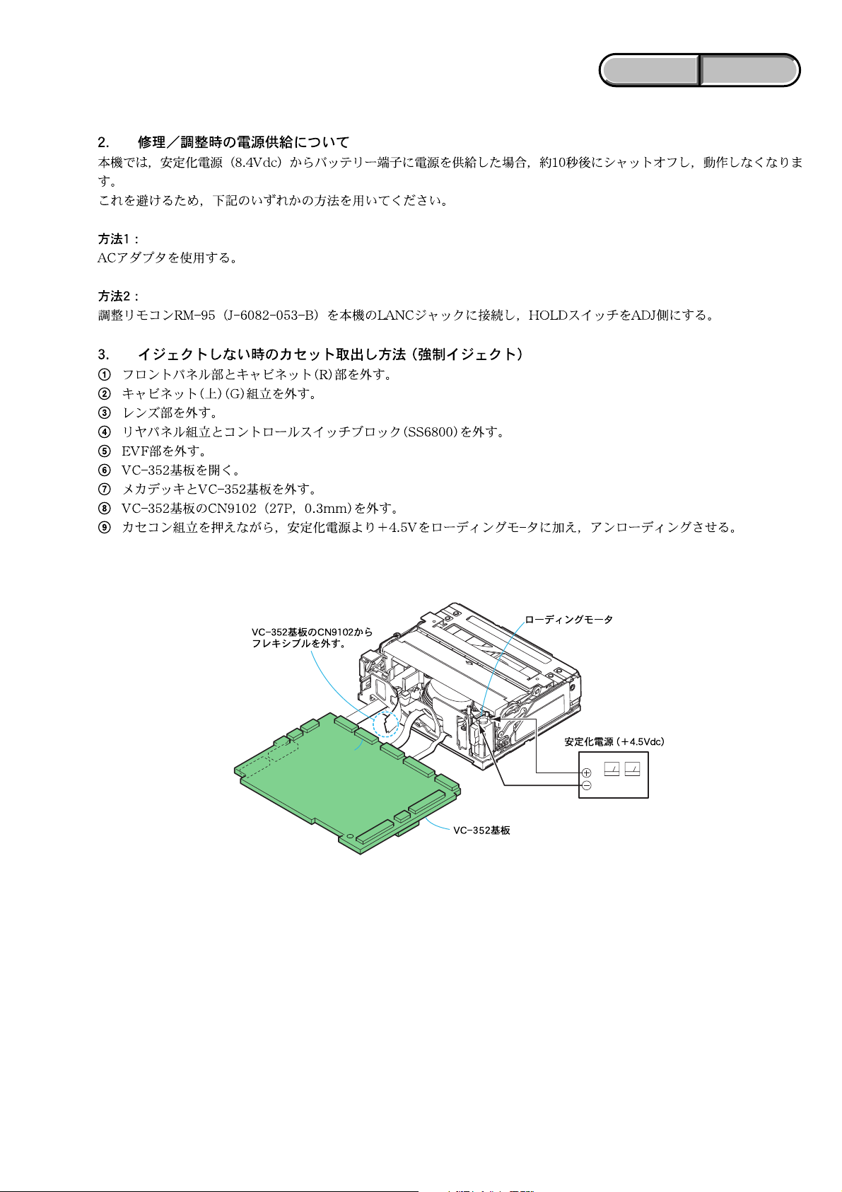
3. TO TAKE OUT A CASSETTE WHEN NOT EJECT (FORCE EJECT)
1 Remove the front panel section and cabinet (R) section.
2 Remove the cabinet (upper) (G) assembly.
3 Remove the lens section.
4 Remove the rear panel assembly and control switch block (SS6800).
5 Remove the EVF section.
6 Open the VC-352 board.
7 Remove the mechanism deck and the VC-352 board.
8 Disconnect CN9102 (27P, 0.3mm) of VC-352 board.
9 Supply +4.5V from the DC power supply to the loading motor and unload with pressing the cassette compartment.
Disconnect the flexible board from
CN9102 of VC-352 board.
CN9102
VC-352
Loading motor
DC power supply (+4.5Vdc)
VC-352 board
1-2
DCR-PC109/PC109E
SECTION 1
SERVICE NOTE
ENGLISH JAPANESE
ENGLISH JAPANESE
1-3
DCR-PC109/PC109E
ENGLISH JAPANESE
ENGLISH JAPANESE
CN9102
VC-352
1-4E
k
SECTION 2
DISASSEMBLY
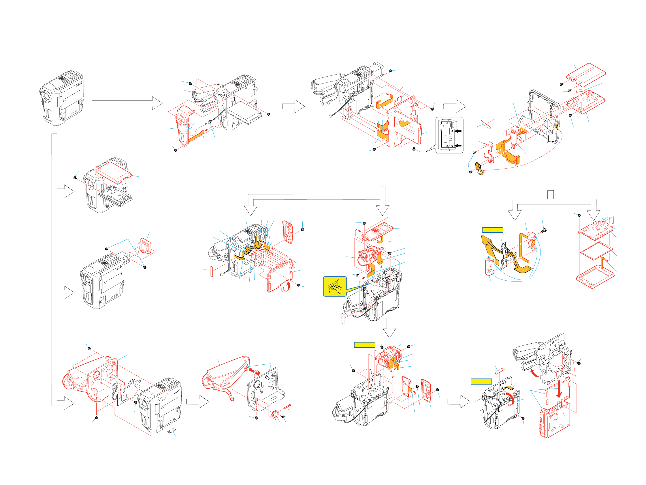
The following flow chart shows the disassembly procedure.
2-1. DISASSEMBLY
DCR-PC109/PC109E
6
4
1
1
Two screws (M1.7x3) black
2
P cabinet (C) (G) assembly
1
Two screws (M1.4x2) black
2
Eye cup assembly
1
1
2
4
7
5
8
7
3
1
Two screws (M1.7x4) silver
2
Open the cassette lid.
3
Screw (M1.7x2.5) silver
4
2
2
1
Screw (M1.7x4) silver
1
2
3
4
5
CN5001 (33P), CN9102 (27P), CN9103 (27P), CN5101 (29P),
CN1205 (20P), CN9101 (10P), CN6501 (10P)) of VC-352 board.
qh
6
5
Claw
6
FP-840 board (16P)
7
Harness (RR-057) (2P)
8
Front panel assembly (G)
7
VC
-352
2
1
qh
4
q;
qa
3
Screw (M1.7x4) silver
Rear panel assembly
qd
8
9
6
5
qs
qg
qf
CR shield sheet
Screw (M1.7x2.5) silver
to qg (CN9301 (20P), CN1201 (18P), CN1203 (10P), CN1208 (39P)
VC-352 board
1
Screw (M1.7x2.5) silver
2
Two screws (M1.7x4) silver
3
Two screws (M1.7x4) silver
4
Screw (M1.7x4) silver
5
FP-841 flexible board (26P)
2
8
7
4
8
9
1
6
7
8
9
q;
5
6
3
q;
2
BT flexible adhesive sheet
FP-848 flexible board (22P)
FP-926 flexible board (6P)
FP-846 flexible board (51P)
Cabinet (R) section
3
1
7
6
5
1
Microphone unit (MEGA) (6P)
2
Two screws (M1.7x2.5) silver
3
Cabinet (upper) (G) assembly
4
CR insulating sheet
5
Flexible board (from lens device) (29P)
6
FP-839 flexible board (33P)
7
Two screws (M1.7x2.5) silver
8
Lens block assembly
4
5
8
1
3
qa
2
1
Tape (A)
2
Three tapping screws (M1.7x5) black
3
Hinge blind
1
3
HELP 03
5
4
1
Screw (M1.7 × 2.5) silver
2
Four claws
3
Hinge cover (M), FP-926 flexible board
4
Hinge cover (C)
5
FP-848 flexible board,
2
Hinge (63) assembly
9
4
Two screws (M1.7x3) black
5
Tapping screw (M1.7x3.5) blac
6
P cabinet (C) (G) assembly
7
Tape (A)
8
FP-848 flexible board (22P)
9
Screw (M1.7x2.5) black
q;
LCD panel section
qa
Hinge section
2
1
Control key block (SB6800) (6P)
2
Tapping screw (M1.7x5) black
3
Two claws
4
TP cushion
5
P cabinet (M) assembly
6
PD-213 board,
LCD unit (ACX528AKP-J),
7
q;
3
6
4
1
5
Light guide plate block
HELP 01
4
6
1
qa
q;
qs
9
8
7
6
1
5
1
1
Four screws (M1.7x2.5) silver
2
Eject knob
3
Two tapping screws (M1.7x3.5) black
4
Cabinet (G) section
6
HELP 02
1
3
2
3
1
Release the lock
2
2
Screw (M1.7x2.5) silver
3
Tapping screw (M1.7x3.5) black
2
4
Belt shaft
5
Belt bracket (front)
6
Grip belt assembly
4
3
5
1
Screw (M1.7x4) silver
2
Rear panel assembly
3
Screw (M1.7x2.5) silver
4
Control switch block (SS6800) (18P)
5
Control switch block (SS6800)
6
FP-842 flexible board (20P)
7
FP-845 flexible board (10P)
8
FP-843 flexible board (39P)
9
Screw (M1.7x4) silver
q;
Tapping screw (M1.7x3.5) black
qa
Two screws (M1.7x4) silver
qs
EVF section
4
5
1
Tape (A)
2
FP-844 flexible board (20P)
3
Screw (M1.7x2.5) silver
4
Return the VC-352 board.
2
7
4
3
VC-352
5
Four screws (M1.4x1.5) silver
6
Open the cassette lid.
7
VC-352 board, Mechanism deck.
2-1 2-2
DCR-PC109/PC109E
)
2-2. SERVICE POSITION
2. DISASSEMBLY
2. DISASSEMBLY
1
2
[SERVICE POSITION TO CHECK THE VTR SECTION]
Connection to Check the VTR Section
To check the VTR section, set the VTR to the "Forced VTR power ON" mode.
Operate the VTR functions using the touch panel. (When the control switch block (ZM6800) is removed, the function
4
8
3
5
7
6
buttons of the adjustment remote commander are not effective even if the HOLD switch of the adjustment remote
commander is set to the OFF position.)
Setting the "Forced VTR Power ON" mode
1) Select page: 0, address: 01, and set data: 01.
2) Select page: 0, address: 10, and set data: 00.
3) Select page: A, address: 10, set data: 02, and press the
PAUSE button of the adjustment remote commander.
Exiting the "Forced VTR Power ON" mode
1) Select page: 0, address: 01, and set data: 01.
2) Select page: 0, address: 10, and set data: 00.
3) Select page: A, address: 10, set data: 00, and press the
PAUSE button of the adjustment remote commander.
4) Select page: 0, address: 01, and set data: 00.
4
5
6
3
7
8
q;
9
1
2
1
6
2
7
4
3
VC-352
5
5
FP-848 Flexible
board (22P)
7
CN1206
Cabinet (R) section
VC-352 board
CN9103
CN9102
CN9101
VC-352
CN6501
CN1208
Mechanism deck
LANC
Adjustment remote
commander (RM-95
CN1207
3
1
2
2
3
1
7
8
7
4
6
5
4
3
2
qa
q;
9
1
8
q;
qs
9
8
7
6
3
4
5
6
CN2101
FP-841 Flexible
board (26P)
1
2
Battery terminal board,
FP-841 flexible board
CN1201
DC-IN
AC power
adaptor
FP-843 Flexible
board (39P)
1
To eject a cassette, connect the
control switch block (SS6800)(18P)
8
AC IN
CPC-15
(J-6082-564-A)
I/F unit for LANC control
(J-6082-521-A)
2-3 2-4
)
[PD-213 BOARD SERVICE POSITION]
2. DISASSEMBLY
2. DISASSEMBLY
DCR-PC109/PC109E
PD-213 board
1
2
Adjustment remote
LANC
commander (RM-95
AC IN
AC power
adaptor
3
1
-2
D
P
2-5
DCR-PC109/PC109E
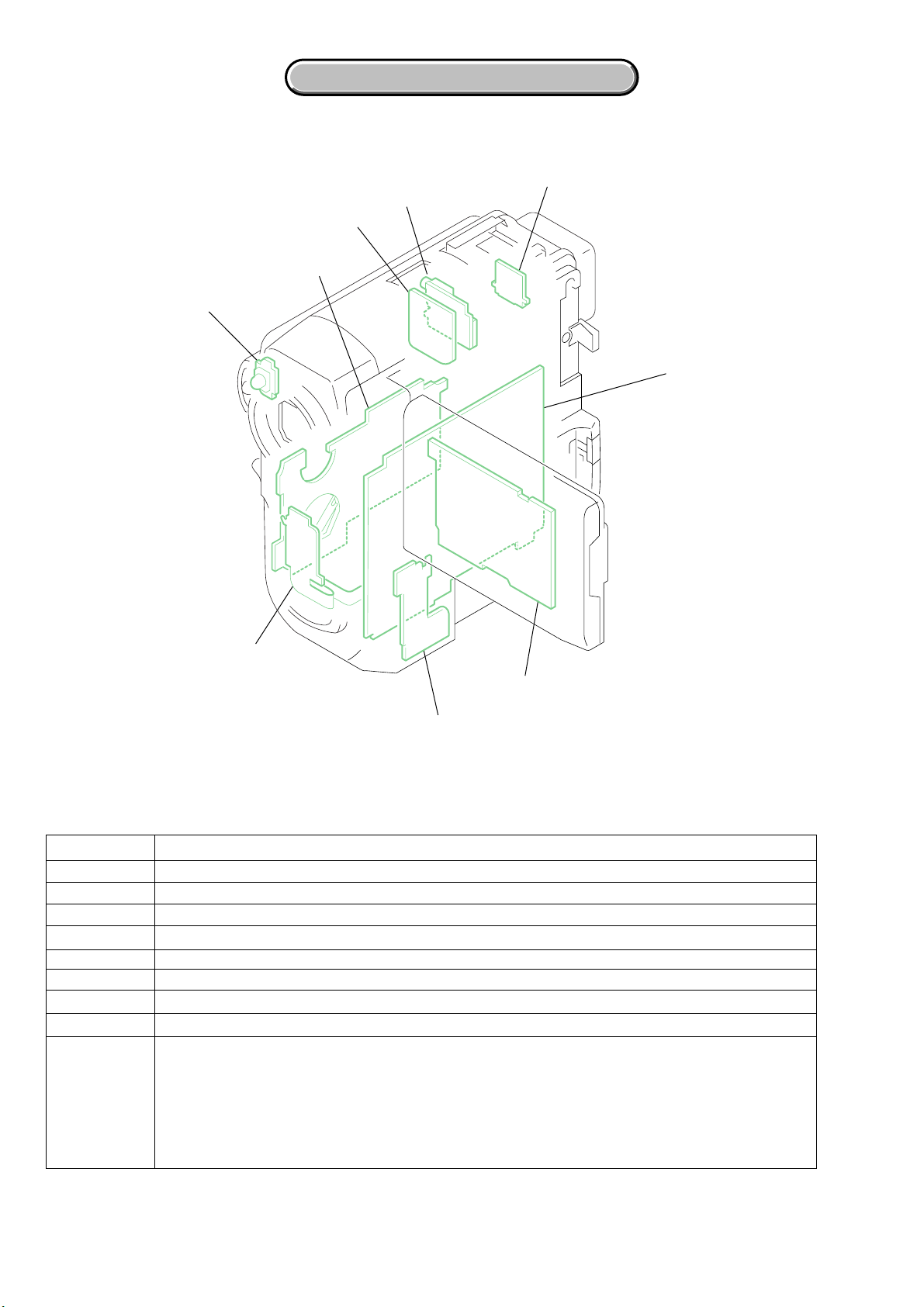
2-3. CIRCUIT BOARDS LOCATION
MS-201
IR-052
CD-494
2. DISASSEMBLY
2. DISASSEMBLY
SE-140
LB-096
VC-352
NAME
CD-494
CR-047
FP-840
IR-052
LB-096
MS-201
PD-213
SE-140
VC-352
FP-840
PD-213
CR-047
FUNCTION
CCD IMAGER
CRADLE CONNECTOR
SIRCS, FRONT INDICATOR
NIGHT SHOT
EVF RELAY
MS CONNECTOR
LCD RGB DRIVE, BACKLIGHT
PITCH/YAW SENSOR AMP, MIC IN
TIMING GENERATOR, S/H, AGC, A/D CONV., LENS DRIVE, CAMERA PROCESS,
MPEG MOVIE/DIGITAL STILL PROCESS, 64Mbit SDRAM, BUFFER, HI/DIGITAL STILL
CONTROL, 32Mbit FLASH, 16Mbit SDRAM, DV SIGNAL PROCESS, DV INTERFACE,
REC/PB AMP, VIDEO I/O, DRUM/CAPSTAN/LOADING DRIVE,CAMERA/MECHA CONTROL,
HI CONTROL, EVF VIDEO, AUDIO I/O, MIC AMP, DC IN, CHARGE, DC/DC CONVERTER,
CONNECTOR
2-6
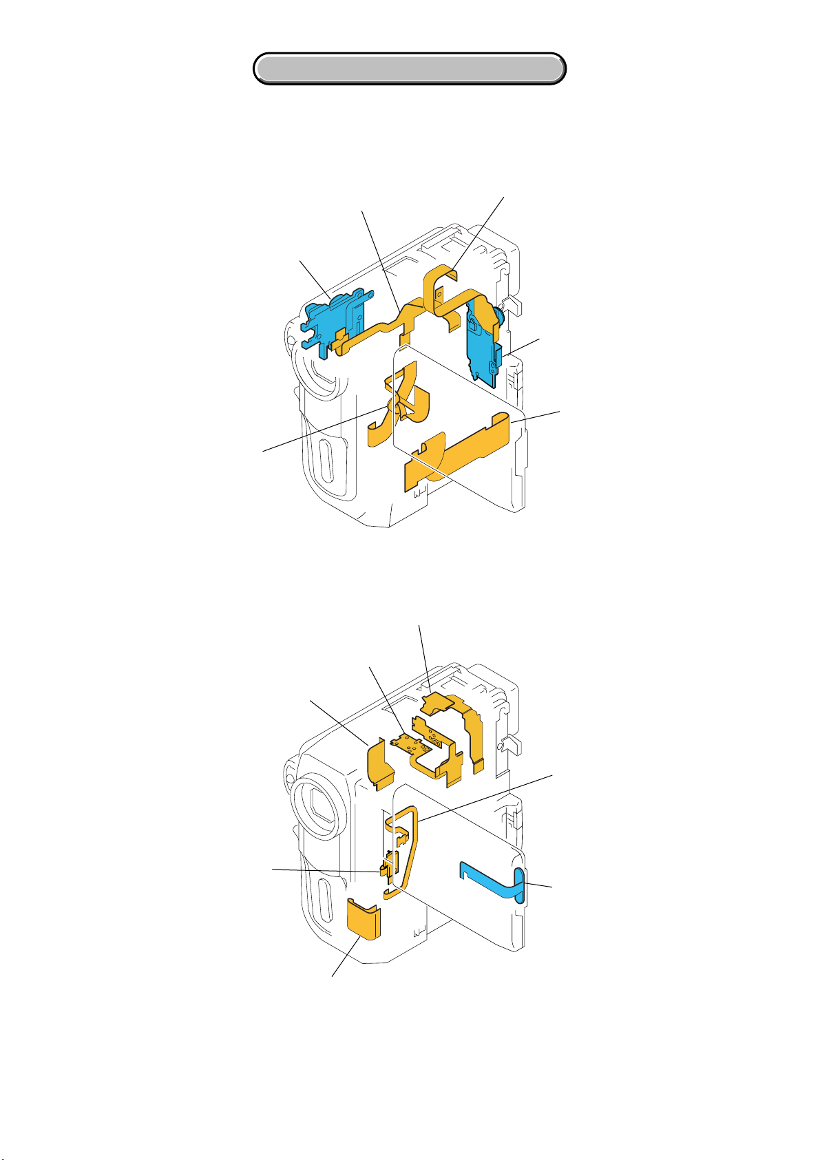
2. DISASSEMBLY
K
2. DISASSEMBLY
2-4. FLEXIBLE BOARDS LOCATION
The flexible boards contained in the lens block is not shown.
DCR-PC109/PC109E
CONTROL SWITCH BLOCK
(ZM6800)
FP-848
FP-844
FP-842
CONTROL SWITCH BLOC
(SS6800)
FP-841
FP-847
FP-845
FP-843
FP-839
FP-926
CONTROL KEY BLOCK
(SB6300)
FP-846
2-7E
DCR-PC109/PC109E
HELP
Sheet attachment positions and procedures of processing the flexible boards/harnesses are shown.
HELP 01
8
Two Tapping screws
(M1.7
black
4
SE-140 board
3
Craw
2
Tapping screw
×
(M1.7
black
3.5),
7
5
Tapping screw
×
(M1.7
black
×
3),
1
FP-843 flexible
board (14P)
q;
FP-843 flexible board,
E parts holder assembly
3.5),
9
Craw
Shoe frame (N)
6
Two craws
ASSEMBLING THE FP-843 FLEXIBLE BOARD
Two Tapping screws
×
3),
(M1.7
black
E parts holder assembly
FP-843 flexible board
HELP
DCR-PC109/PC109E
HELP 02
Cutout of the control switch block (ZM6800)
Harness (RR-057)
HELP 03
3
Hinge (63) assembly
2
Unwind the FP-848 flexible
board wide open.
1
Peel off the adhesive surface.
Adhesive surface
HELP
4
FP-848 flexible board

Link
Link
DCR-PC109/PC109E
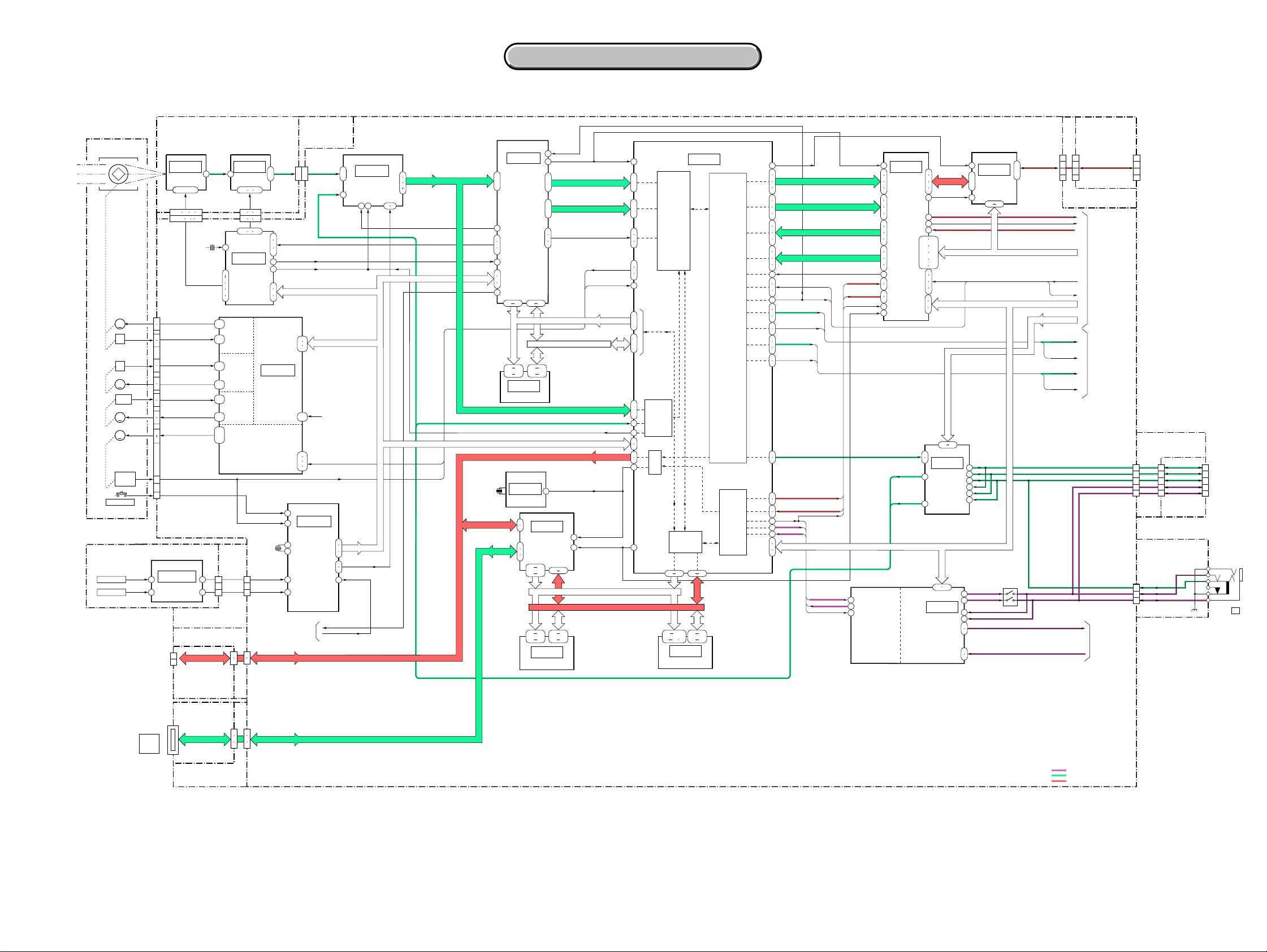
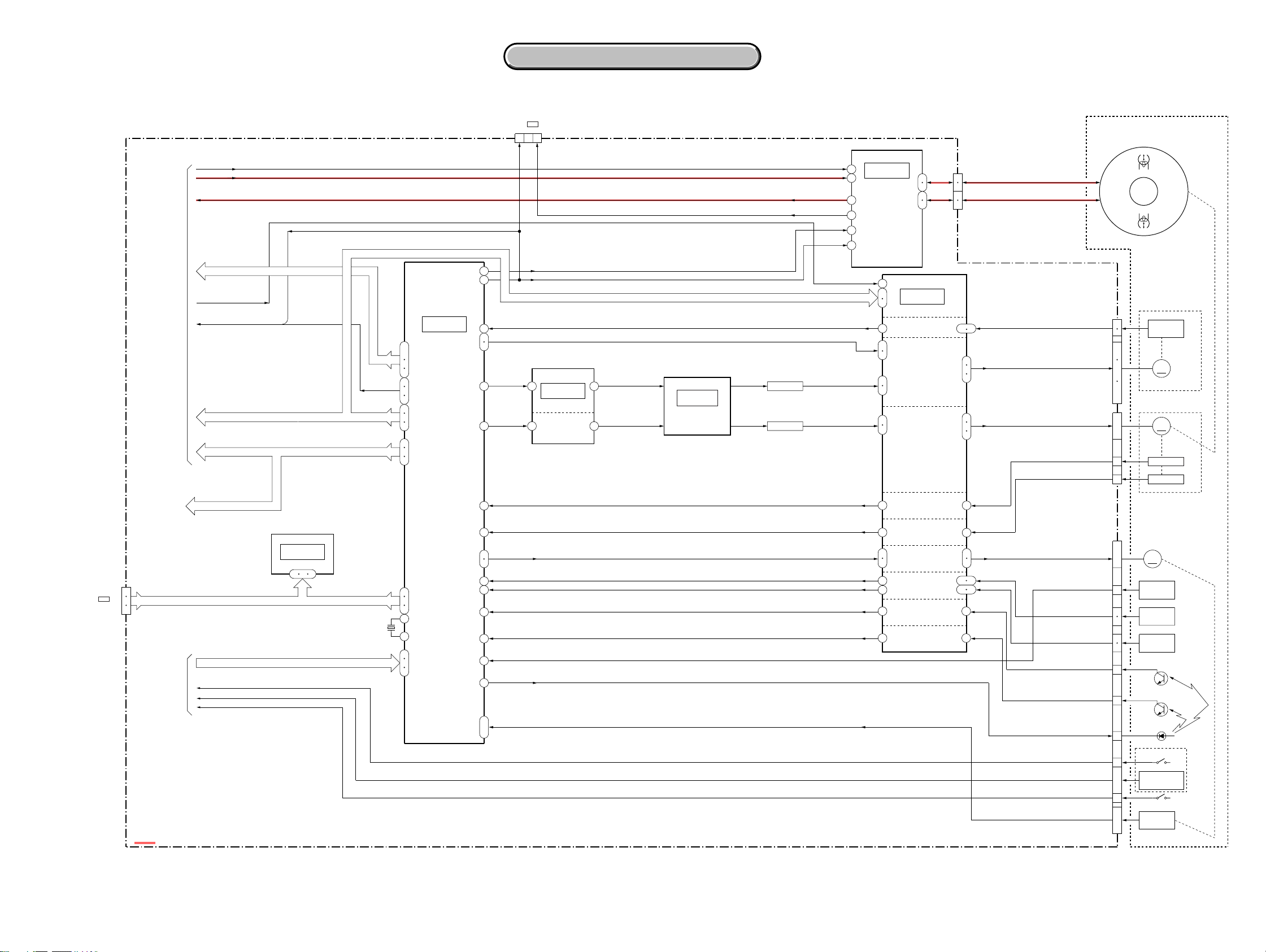
3. BLOCK DIAGRAMS
OVERALL BLOCK DIAGRAM (1/4)
OVERALL BLOCK DIAGRAM (2/4) POWER BLOCK DIAGRAM (2/2)
OVERALL BLOCK DIAGRAM (3/4)
OVERALL BLOCK DIAGRAM (4/4)
POWER BLOCK DIAGRAM (1/2)
DCR-PC109/PC109E
BLOCK DIAGRAMS
3-1. OVERALL BLOCK DIAGRAM (1/4)
ND FILTER
METER
FOCUS
MOTOR
ZOOM
MOTOR
SE-140
BOARD
SE402
YAW SENSOR
SE401
PITCH SENSOR
LENS ASSY
(SHUTTER)
NIGHT SHOT
IRIS
M
M
MR
M
M
H
H
ZOOM
RESET
SENSOR
CD-494 BOARD
IC201
12
CCD
IMAGER
4-1 14 16 18
•••
V1-V4
RG,H1,H2
CN201
7-4
24 21 22
26-29
5 7 8
CN5001
X5001
66MHz : PC109
54MHz : PC109E
IRIS DRIVE
23
+,-
22
IRIS HALL
+,-
21
25
ND HALL
17
+,-
15
ND DRIVE
12
+,-
13
2
FMR A,B
1
10
FOCUS +,-
11
6
ZOOM A,XA,B,XB
9
ZOOM RST ZOOM RST
26
XNS SW
18
CN5101
IC401
12
8
TO
CRADLE
YAW/PITCH
SENSOR
AMP
FP-843
(FLEXIBLE)
FP-846
(FLEXIBLE)
32
34
18
2
USB D+,D-
IC202
5
13 14 1
19 18 13
11 12 18
38 33 64
(1/21)
CDS
•
4
XSHD,XSHP,CLPDM
CN201
CN5001
11
47
IC5001
TIMING
67
GENERATOR
73
32
17
25
H1
J1
IRIS
DRIVE
C5
B6
ZOOM MOTOR
37
35
CN1208
DRIVE
IC5101
X8801
20MHz
YAW AD
PITCH AD
(2/21)
C10
ND
B11
FILTER
DRIVE
K2
L2
B1
C4
FOCUS
MOTOR
DRIVE
F3
E3
K6
L4
F1
G3
12
10
CN402
(1/4)
(1/4)
CN1211
CN802CN801
7
44
45
USB D+,D-
8
CR-047
BOARD(1/4)
MS-201
CN503
MEMORY
STICK
DUO
CONNECTOR
BOARD(1/3)
MS BS,DIO,SCLK
CN1205
12
6
11
5
MS BS,DIO,SCLK
8
3
CN501
FP-839
(FLEXIBLE)
CCD OUT
14
15
+,-
••
15
16
CN5001CN201
IC1701 Y OUT
9
HD,VD,FLD HD,VD,FLD
10
12
CHCK CHCK
53
ADCK27
59
5
CAM SO,SI,SCK
2
1
J11
K11
H12
K12
SPCK
(IC6201)
EN1
K9
DIR1A
L9
DIR1B
M9
J9
(13/21)
187
IC8801
54
CAMERA CONTROL
1
3
130
129
TO
OVERALL
1
BLOCK DIAGRAM
(4/4)
(PAGE 3-8)
SECTION 3
3. BLOCK DIAGRAMS
3. BLOCK DIAGRAMS
( ) : Number in parenthesis ( ) indicates the division number of schematic diagram where the component is located.
VC-352 BOARD(1/4)
(1/2)
EXT STROBO
ZOOM VR AD
77
75
73
71
135
78
30
•
31
34
CAM SO,SI,SCK
CH SO,SCK
(1/21)
IC5003
S/H, AGC
A/D CONV.
16
20
44 45
CH SO,SCK
IC7101 Y OUT
(3/21)
IC5201
CAMERA
47
48
AD0-AD13
AD0-AD13
1
12
AD0-AD13
EXT STROBO
PROCESS
56
|
71
CLPOB
77
92
91
90
137
22
23
20
102
161 144
A0-A10, A12
26
20
35
29
IC6202
64Mbit
SDRAM
SPCK
122
VCK
115 241
208
D0-D15A0-A13
195 174
213
42
|
199
9
|
6
11
12
13
53
A0-A13
D0-D15
IFI Y0-Y7
IFI C0-C3
IFI HD
IFI VD
IFI OE
(5/21)
CAM SO,SI,SCK
USB D+,D-
ZOOM RST
AD4-AD13
IC7101 C OUTIC7101 C OUT
DO-D15
DIR1A
DIR1B
ADCK27
216
|
223
224
|
227
228
229
230
EN1
248
250
251
238
185
|
170
215
|
198
252
|
VIDEO
261
A/D
CONV.
33
245
158
156
28
USB
29
I/F
24
(7/21)
X8401
48MHz
USB D+,D-
MS BS,DIO,SCLK
MS BS
MS DIO
MS SCLK
IC8403
XTAL
OSC
185
186
85
81
78
291 304
20 26
29
USB CLK
4
(6/21)
IC8401
(1/2)
DIGITAL
STILL
CONTROL
A1-A22
D0-D15
16 35
1
12
213
35
42
53
IC8502
16Mbit
(7/21) (7/21)
SDRAM
USB CLK
177
DSCK VM
119122
A1-A22
D0-D15
A1-A19 D0-D15
IC6201
MPEG
MOVIE
PROCESS
DIGITAL
STILL
PROCESS
116 98 121 137
25 16,13
29 36
38
10 148
IC8503
32Mbit
FLASH MEMORY
(4/21)
20
268
269
RYO0-RYO3,DEHD,DEVD.DEFLD.SGOUT
270
271
279
280
RCO0-RCO3,EDHD,EDVD.EDFLD.FRMREF
281
282
264
265
266
267
272
DV
SIGNAL
PROCESS
AUDIO
SIGNAL
PROCESS
45
273
275
276
284
168
86
169
139
47
46
52
95
96
40
39
45
92
93
53
60
301
302
298
299
82
89
87
151
152
150
FRRV
TRRT
TRRV
SPCK
EVF R
EVF G
EVF B
EVF HD
EVF VD
PANEL R
PANEL G
PANEL B
PANEL HD
PANEL VD
IC6201 Y OUT
IC6201 C OUT
ADATAIN0
ADATAIN1
ADATAOUT0
ADATAOUT1
SFD BCK
DATA FROM SFD
DATA TO SFD
VSP SO,SI,SCK
RYI0-RYI3,DE0-DE3
RCI0-RCI3,DE4-DE7
DATA FROM SFD
DATA TO SFD
SFD BCK
143 79
IC6401
119
162
120
PROCESS
163
PROCESS
70
121
71
122
13
72
14
73
123
166
124
125
HY1 PLL 27INHY1 PLL 27IN
12
ADATAIN0
168
ADATAIN1
127
ADATAOUT0
167
ADATAOUT1
126
SFD BCK
21
DSCK VM
15
IC7101 C OUT
26
27
D/A CONV.
A/D CONV.
34
(8/21)
DV
SIGNAL
RF
SIGNAL
IC7101 Y OUT
149
186
150
187
139
54 107
152 189
55 153
190 109
155 192
112
111
114
157
46
7
34
36
LBUS0-LBUS3
TRCK0
45
41
60
58
3
IC7101
38 35
(16/21)
IC7601
AUDIO
SWP
FRRV
TRRT
TRRV
VSP SO,SI,SCK
DO-D15
910
(11/21)
VIDEO
IN/OUT
AGC
ACC
I/O
LCK0LCK0 VCK
VD SO,SCK
2
4
57
62
17
16
71
77
CR-047
BOARD(2/4)
45
|
42
47104
(9/21)
IC6301
DV
INTERFACE
29 37
CN802
CN1211
14
MC BUSMC BUS
VSP SO,SI,SCK
VD SO,SCK
15
13
12
REC DTREC DT
REC CKREC CK
EVF HD
EVF VD
PANEL R
PANEL G
PANEL B
PANEL HD
PANEL VD
EVF R
EVF G
EVF B
38
37
39
40
FP-846
(FLEXIBLE)(2/4)
RF INRF IN
SWP
2
FRRV
TRRT
TRRV
SPCK
3
TPA +, –
TPB +, –
9
|
6
TO
OVERALL
BLOCK DIAGRAM
(3/4)
(PAGE 3-5)
TO
OVERALL
BLOCK DIAGRAM
(2/4)
(PAGE 3-3)
CN801
TPA
NTPA
31
TPB
29
NTPB
TO
CRADLE
33
35
FP-846
(FLEXIBLE)(3/4)
4
AUDIO L I/O
AUDIO R I/O
TO
OVERALL
BLOCK DIAGRAM
(2/4)
(PAGE 3-3)
CN1211
VIDEO I/O
CN1208
28
24
26
26
23
29
19
33
21
31
CN802
CR-047
BOARD(3/4)
FP-843
(FLEXIBLE)(2/4)
11
16
14
VIDEO I/O
AUDIO L
AUDIO R
S Y
9
S C
13
TO
10
CRADLE
18
14
CN801
L
V
R
J002
A/V
Y
18
C
14
V
22
Y
39
C
48
V
42
L
R
L
R
SP+
SP-
MIC L
MIC R
SP+
SP-
MIC L
MIC R
FP-844
(FLEXIBLE)
16
(1/3)
3-1 3-2
AUDIO SIGNAL
VIDEO SIGNAL
VIDEO/AUDIO SIGNAL
DCR-PC109/PC109E
3. BLOCK DIAGRAMS
3. BLOCK DIAGRAMS
3-2. OVERALL BLOCK DIAGRAM (2/4)
FP-843
(FLEXIBLE)(3/4)
2
4
8
6
MIC901
J401
MIC
(PLUG IN POWER)
MIC
MIC
L
R
16
SE-140 BOARD
CN401 CN1208CN402
5
3
( ) : Number in parenthesis ( ) indicates the division number of schematic diagram where the component is located.
VC-352 BOARD(2/4)
FP-848 (FLEXIBLE)
(1/2)
CN1206 CN601
PANEL R,G B
HD
TO
5
OVER ALL
BLOCK DIAGRAM (3/4)
(PAGE 3-5)
TO
3
OVER ALL
BLOCK DIAGRAM (1/4)
VD,SO,SI,SCK
PANEL R
PANEL G
PANEL B
PANEL HD
PANEL VD
EVF R
EVF G
EVF B
EVF R,G,B
(15/21)
34
33
IC9301
32
RGB
DRIVE
(PAGE 3-2)
45
42
TIMING
EVF HD
EVF VD
EVF HD
EVF VD
(15/21)
IC9302
SP+
MIC L
MIC R
SHOE MIC L
SP-
MIC L
MIC R
TO
4
OVER ALL
BLOCK DIAGRAM (1/4)
(PAGE 3-2)
(17/21)
28
30
33
31
35
IC7701
MIC AMP
1
R
3
L
33
22
14
36
48
GENERATOR
44
48
1
18
BL ON EXTDA
BACKLIGHT
Q9303
DRIVE
VD
20
22
21
26
25
24
17
6
31
1
2
3
12
13
22
19
21
FP-842 (FLEXIBLE)
CN9301
15
14
13
17
16
12
3
10
20
18
19
CN1205
FP-844 (FLEXIBLE)
(2/3)
CN1203
3
FP-845 (FLEXIBLE)
SHOE MIC L
(1/2)
PD-213 BOARD(1/2)
1
2
3
12
13
22
19
21
LB-096 BOARD
6
7
8
4
5
9
EN, VST, REF, PCG, VCK, XSTBY,BLK,HCK1/2, HST
18
LED. K
1
CN301
12
13
CN501
MS-201 BOARD (2/3)
INTELLIGENT
2
ACCESSORY
SHOE (1/2)
34
33
32
42
45
44
48
1
BL ON EXTDA
IC601
Q604-607
R,G,B
COM
PSIG
SP+, SP-
IC602
RGB
DRIVE
TIMING
GENERATOR
18 31
BACK LIGHT
DRIVE
D303
BACK
LIGHT
CN302
CN502
20
21
22
26
17
5
VR,VG,VB
COM
17
18
16
21
19
20
15
5
1
2
LCD902
COLOR
EVF
UNIT
BL -15.5V
SP901
SPEAKER
COM
COS
CN607
CN608
LCD901(1/2)
4
5
3
24
23
22
19
14
6
2
BACK LIGHT
1
3
AUDIO SIGNAL
VIDEO SIGNAL
2.5 INCH
COLOR
LCD UNIT
BL H
BL L
ND901
3-3 3-4
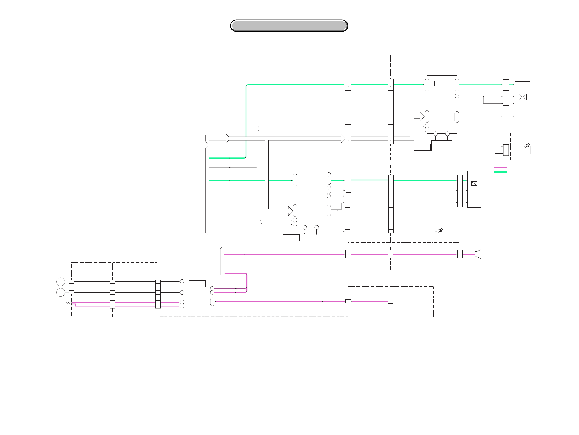
3. BLOCK DIAGRAMS
3. BLOCK DIAGRAMS
DCR-PC109/PC109E
3-3. OVERALL BLOCK DIAGRAM (3/4)
CPC
CN1207
FOR ADJUSTMENTS
VC-352 BOARD(3/4)
TO
OVERALL
2
BLOCK DIAGRAM
(1/4)
(PAGE 3-2)
TO
5
OVERALL
BLOCK DIAGRAM
(1/4)
(PAGE 3-3)
6
7
5
TO
6
OVERALL
BLOCK DIAGRAM
(4/4)
(PAGE 3-8)
16
DIGITAL VIDEO/AUDIO SIGNAL
EEP SO, SI, SCK
REC CK
REC DT
RF IN
MC BUS
SPCK
SWP, FRRV, TRRT, TRRV
VSP SO,SI,SCK
VD SO, SCK
VD SO, SI, SCK
HI SO,SI,SCK
REC PROOF
CHIME SDA,CHIME SCK,CHIME VDD
XCC DOWN
SWP
(13/21)
IC8802
EEPROM
562
( ) : Number in parenthesis ( ) indicates the division number of schematic diagram where the component is located.
CPC
CN1207
FOR ADJUSTMENTS
21
VSP SO,SI,SCK
X8801
20MHz
FRRV
TRRT
TRRV
SWP
172
164
(13/21)
IC8801
52
|
45
33
32
23
178
179
69
70
67
82
83
80
86
87
84
1
3
66
65
63
MECHA
CONTROL
(2/2)
CAP FG
190
CAP ON,CAP FWD
165
166
CAP PWM
89
DRUM PWM
88
DRUM FG
197
DRUM PG
198
LOAD,UNLOAD
15
13
TREEL FG
192
SREEL FG
193
TAPE END
31
TAPE TOP
30
DEW AD
119
TAPE LED ON
180
106
MODE SW A - MODE SW C
|
108
41
44
RF MON
(12/21)
IC9101
LPF
LPF
(2/2)
REC CK
REC DT
RF IN
RF MON
RF SWP
SWP
VSP SO, SCK
43
CAP ERROR
(19/21)
24
75
Q2305
SWITCHING
IC2301
(1/2)
PWM
45
DRUM ERROR
21
DRIVE
77
Q2306
SWITCHING
(10/21)
44
IC6501
46
REC/PB
AMP
35
30
39
38
35
38
36
4
80
1
75
CAP VS
77
64
DRUM VS
67
53 52
50
32
33
29
25
21
19
Z MECHA DECK
CN6501
ODD
EVEN 3
5
6
2
DRUM
10
9
4
3
(12/21)
IC9101
(1/2)
CAPSTAN
FG AMP
CAPSTAN
MOTOR
DRIVE
DRUM
MOTOR
DRIVE
DRUM FG AMP
DRUM PG AMP
LOADING MOTOR
DRIVE MOTOR
REEL FG AMP
TAPE END DETECT
TAPE TOP DETECT
7 8
26 27
22 23
FG 1,2
74
CAP U,V,W
76
78
63
DRUM U,V,W
65
68
49
69
72
20
18
CN9103
CN9101
CN9102
LM +, –
DEW AD
T REEL +, –
S REEL +, –
XCC DOWN
22
25
20
17
4
1
11
14
10
26
25
22
23
20
11
18
12
13
15
17
|
|
|
6
|
1
9
1
|
4
5
|
7
|
9
DRUM FG
DRUM PG
M
DEW
SENSOR
T REEL
SENSOR
S REEL
SENSOR
Q901
TAPE END SENSOR
Q902
TAPE TOP SENSOR
D901
TAPE LED
(REC PROOF)
CONNECTOR
(C. C. DOWN)
MODE
SWITCH
S902
M903
CAPSTAN
FG
M
M901
M
4PIN
CAPSTAN
MOTOR
DRUM
MOTOR
M902
LOADING
H902
H901
S903
MIC902
3-5 3-6
 Loading...