

Page 1
CDX-CA900/CA900X
SERVICE MANUAL
Ver 1.0 2002. 04
• The tuner and CD sections have no adjustments.
AUDIO POWER SPECIFICATIONS (US Model)
POWER OUTPUT AND TOTAL HARMONIC DISTORTION
23.2 watts per channel minimum continuous average power into
4 ohms, 4 channels driven from 20 Hz to 20 kHz with no more
than 5% total harmonic distortion.
SPECIFICATIONS
CD player section
Signal-to-noise ratio 90 dB
Frequency response 10 – 20,000 Hz
Wow and flutter Below measurable limit
Tuner section
FM
Tuning range 87.5 – 107.9 MHz (US, Canadian Model)
87.5 – 108.0 MHz (E Model)
Antenna terminal External antenna connector
Intermediate frequency 10.7 MHz/450 kHz
Usable sensitivity 8 dBf
Selectivity 75 dB at 400 kHz
Signal-to-noise ratio 66 dB (stereo),
72 dB (mono)
Harmonic distortion at 1 kHz
0.6% (stereo),
0.3% (mono)
Separation 35 dB at 1 kHz
Frequency response 30 – 15,000 Hz
AM (US, Canadian Model)
Tuning range 530 – 1,710 kHz
Antenna terminal External antenna connector
Intermediate frequency 10.7 MHz/450 kHz
Sensitivity 30 µV
US Model
Canadian Model
CDX-CA900X
E Model
CDX-CA900
Model Name Using Similar Mechanism NEW
CD Drive Mechanism Type MG-393XA-121//Q
Optical Pick-up Name KSS-720A
Power amplifier section
Outputs Speaker outputs
(sure seal connectors)
Speaker impedance 4 – 8 ohms
Maximum power output 52 W × 4 (at 4 ohms)
General
Outputs Audio outputs (front /rear)
Subwoofer output (mono)
Power antenna relay control terminal
Power amplifier control terminal
Inputs Telephone ATT control terminal
Illumination control terminal
BUS control input terminal
BUS audio input or AUX IN terminal
Remote controller input terminal (E Model)
Antenna input terminal
Tone controls Bass ±10 dB at 62 Hz (US, Canadian Model)
Bass ±8 dB at 100 Hz (E Model)
Treble ±10 dB at 16 kHz (US, Canadian Model)
Treble ±8 dB at 10 kHz (E Model)
Loudness +8 dB at 100 Hz
+2 dB at 10 kHz
– Continued on next page –
MW/LW (E Model)
Tuning range MW : 531 – 1,602 kHz
Aerial terminal External aerial connector
Intermediate frequency 10.7 MHz/450 kHz
Sensitivity MW : 30 µV
9-874-007-01
2002D0400-1
© 2002. 04
LW : 153 – 279 kHz
LW : 40 µV
Sony Corporation
e Vehicle Company
Published by Sony Engineering Corporation
FM/AM COMPACT DISC PLAYER
CDX-CA900X
FM/MW/LW COMPACT DISC PLAYER
CDX-CA900
1
Page 2
CDX-CA900/CA900X
k
Power requirements 12 V DC car battery
(negative ground)
Dimensions Approx. 178 × 50 × 179 mm
(7 1/8 × 2 × 7 1/8 in.) (w/h/d)
Mounting dimensions Approx. 182 × 53 × 162 mm
(7 1/4 × 2 1/8 × 6 1/2 in.) (w/h/d)
Mass Approx. 1.3 kg
(2 lb. 14 oz.)
Supplied accessories Parts for installation and connections (1 set)
Front panel case (1)
Card remote commander (1)
RM-X112 (US, Canadian model)
RM-X113 (E model)
Rotary commander (1) RM-X6S
Note
This unit cannot be connected to a digital preamplifier or an equalizer.
Design and specifications are subject to change without
notice.
SERVICE NOTES
NOTES ON HANDLING THE OPTICAL PICK-UP BLOCK
OR BASE UNIT
The laser diode in the optical pick-up block may suffer electrostatic
breakdown because of the potential difference generated by the
charged electrostatic load, etc. on clothing and the human body.
During repair, pay attention to electrostatic breakdown and also use
the procedure in the printed matter which is included in the repair
parts.
The flexible board is easily damaged and should be handled with
care.
NOTES ON LASER DIODE EMISSION CHECK
The laser beam on this model is concentrated so as to be focused on
the disc reflective surface by the objective lens in the optical pickup block. Therefore, when checking the laser diode emission, observe from more than 30 cm away from the objective lens.
Notes on Chip Component Replacement
• Never reuse a disconnected chip component.
• Notice that the minus side of a tantalum capacitor may be dam-
aged by heat.
CAUTION
Use of controls or adjustments or performance of procedures
other than those specified herein may result in hazardous
radiation exposure.
If the optical pick-up block is defective, please replace the whole
optical pick-up block.
Never turn the semi-fixed resistor located at the side of optical
pick-up block.
optical pick-up bloc
semi-fixed resistor
TEST DISCS
This set can playback CD-R and CD-ROM discs. The following
test discs should be used to check the capability:
CD-R test disc TCD-R082LMT (Part No. J-2502-063-1)
CD-RW test disc TCD-W082L (Part No. J-2502-063-2)
Notes on CD-R/CD-RW discs
• You can play CD-Rs (recordable CDs)/CD-RWs (re writable CDs)
designed for audio use on this unit.
Look for these marks to distinguish CD-Rs/CD-RWs for audio
use.
SAFETY-RELATED COMPONENT WARNING!!
COMPONENTS IDENTIFIED BY MARK 0 OR DOTTED LINE
WITH MARK 0 ON THE SCHEMATIC DIAGRAMS AND IN
THE PARTS LIST ARE CRITICAL TO SAFE OPERATION.
REPLACE THESE COMPONENTS WITH SONY P ARTS WHOSE
PART NUMBERS APPEAR AS SHOWN IN THIS MANUAL OR
IN SUPPLEMENTS PUBLISHED BY SONY.
2
These marks denote that a disc is not for audio use.
• Some CD-Rs/CD-RWs (depending on the equipment used for
its recording or the condition of the disc) may not play on this
unit.
• You cannot play a CD-R/CD-RW that is not finalized∗.
∗ A process necessary for a recorded CD-R/CD-RW disc to be
played on the audio CD player.
ATTENTION AU COMPOSANT AYANT RAPPORT
À LA SÉCURITÉ!!
LES COMPOSANTS IDENTIFIÉS P AR UNE MARQUE 0 SUR LES
DIAGRAMMES SCHÉMATIQUES ET LA LISTE DES PIÈCES
SONT CRITIQUES POUR LA SÉCURITÉ DE FONCTIONNEMENT.
NE REMPLACER CES COMPOSANTS QUE PAR DES PIÈCES
SONY DONT LES NUMÉROS SONT DONNÉS DANS CE MANUEL
OU DANS LES SUPPLÉMENTS PUBLIÉS PAR SONY.
Page 3
TABLE OF CONTENTS
CDX-CA900/CA900X
1. GENERAL
Location of controls (US, Canadian Model) ........................... 4
Location of controls (E Model) ...............................................4
Connections (US, Canadian Model)........................................ 5
Connections (E Model) ........................................................... 6
2. DISASSEMBLY
2-1. Sub Panel Assy .................................................................... 7
2-2. CD Mechanism Block ......................................................... 8
2-3. Main Board ......................................................................... 8
2-4. Heat Sink ............................................................................. 9
2-5. Chassis (T.U) Assy .............................................................. 9
2-6. Disc In Board .................................................................... 10
2-7. Servo Board....................................................................... 10
2-8. Shaft Roller Assy, Load Board .......................................... 11
2-9. Floating Block Assy .......................................................... 11
2-10. Optical Pick-up Block ....................................................... 12
3. DIAGRAMS
3-1. IC Pin Descriptions ...........................................................13
3-2. Circuit Boards Location ....................................................18
3-3. Block Diagram –CD Section–........................................... 19
3-4. Block Diagram –Tuner Section–....................................... 20
3-5. Block Diagram –Display Section–.................................... 21
3-6. Printed Wiring Boards –CD Mechanism Section–............ 22
3-7. Schematic Diagram –CD Mechanism Section– ................ 24
3-8. Schematic Diagram –Main Section (1/4)– ........................ 25
3-9. Schematic Diagram –Main Section (2/4)– ........................ 26
3-10. Schematic Diagram –Main Section (3/4)– ........................ 27
3-11. Schematic Diagram –Main Section (4/4)– ........................ 28
3-12. Printed Wiring Board –Relay Section– .............................29
3-13. Printed Wiring Board –Main Section– .............................. 30
3-14. Printed Wiring Board –Key Section– ................................ 32
3-15. Schematic Diagram –Key Section–................................... 33
4. EXPLODED VIEWS
4-1. Chassis Section ................................................................. 37
4-2. Main Board Section .......................................................... 38
4-3. Front panel Section ........................................................... 39
4-4. CD Mechanism Section (1) ............................................... 40
4-5. CD Mechanism Section (2) ............................................... 41
4-6. CD Mechanism Section (3) ............................................... 42
5. ELECTRICAL PARTS LIST ........................................43
EXTENSION CABLE AND SERVICE POSITION
When repairing or servicing this set, connect the jig (extension cable)
as shown below.
• Connect the MAIN board (CN401) and the SERVO board (CN1)
with the extension cable (Part No. J-2502-062-1).
MAIN BOARD CN401
SERVO BOARD CN1
3
Page 4
CDX-CA900/CA900X
SECTION 1
GENERAL
(US, Canadian Model) (E Model)
This section is extracted
from instruction manual.
(US, Canadian Model) (E Model)
4
Page 5
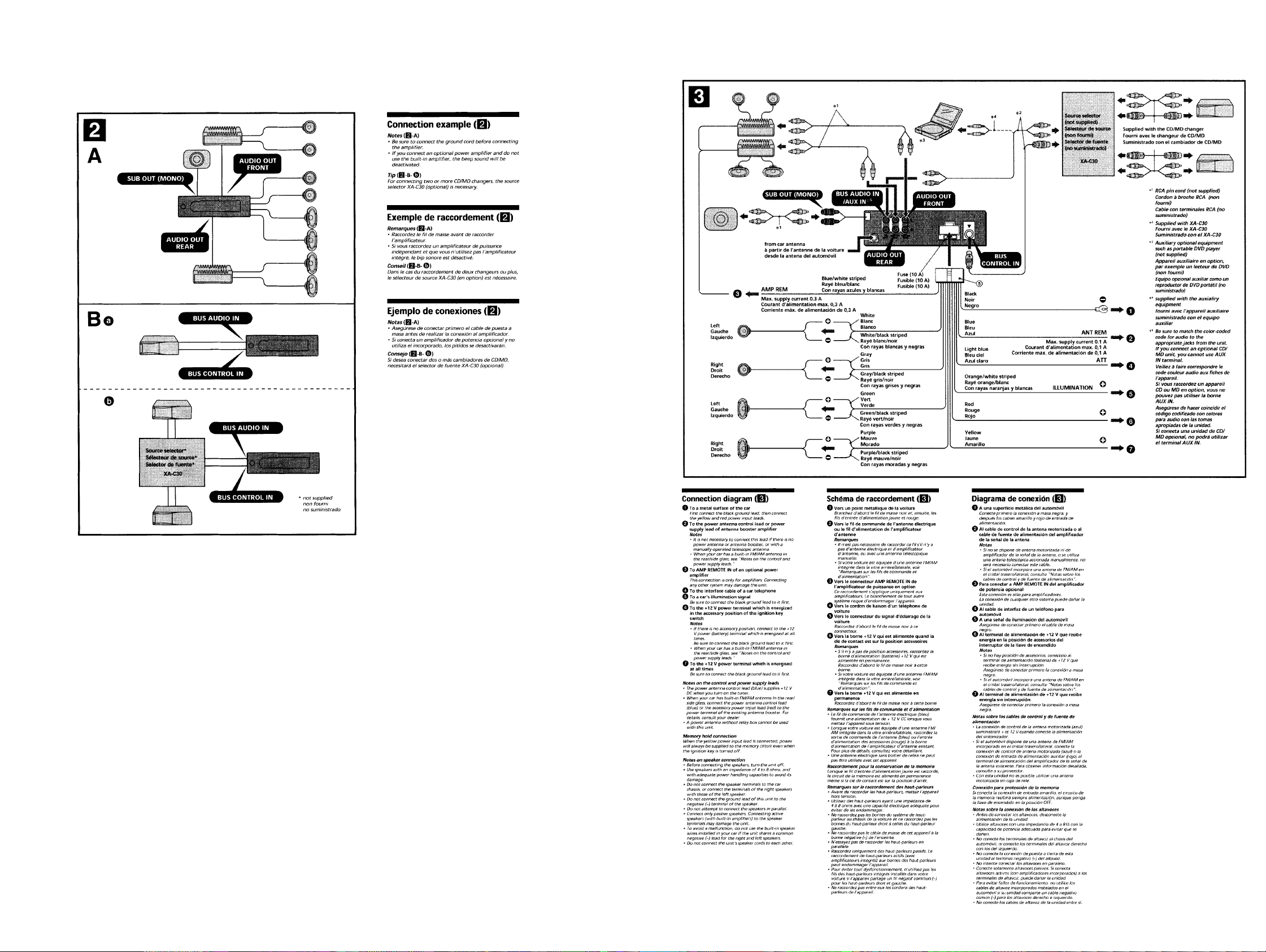
Connections (US, Canadian Model)
CDX-CA900/CA900X
55
Page 6
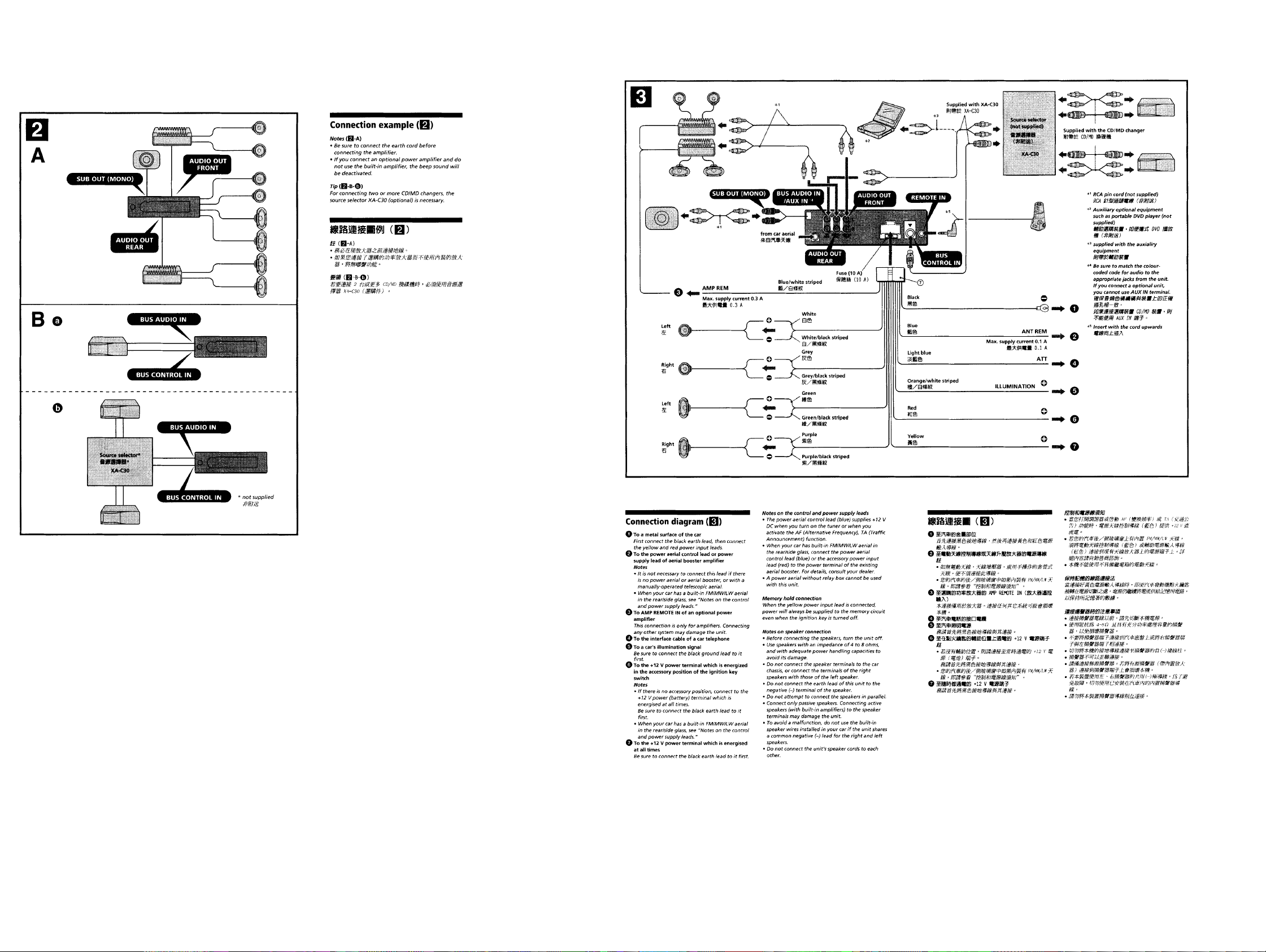
CDX-CA900/CA900X
Connections (E Model)
66
Page 7
SECTION 2
DISASSEMBLY
Note : This set can be disassemble according to the following sequence.
SET
2-5. CHASSIS (T.U) ASSY
(Page 9)
2-1. SUB PANEL ASSY
(Page 7)
2-6. DISC IN BOARD
2-2. CD MECHANISM BLOCK
(Page 8)
2-3. MAIN BOARD
(Page 8)
(Page 10)
2-8. SHAFT ROLLER ASSY,
LOAD BOARD
(Page 11)
CDX-CA900/CA900X
2-7. SERVO BOARD
(Page 10)
2-4. HEAT SINK
(Page 9)
2-9. FLOATING BLOCK ASSY
(Page 11)
2-10. OPTICAL PICK-UP BLOCK
(Page 12)
Note : Follow the disassembly procedure in the numerical order given.
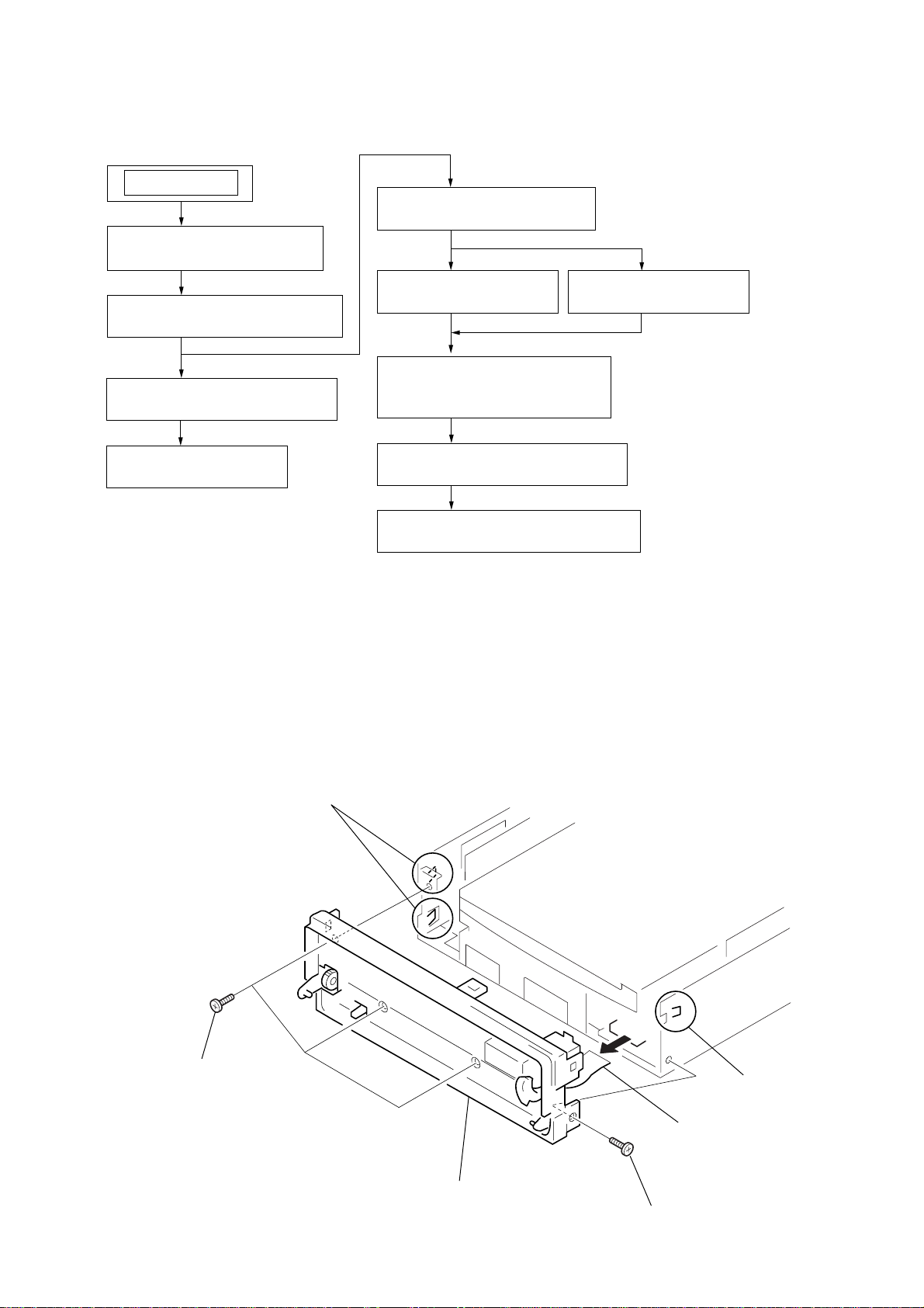
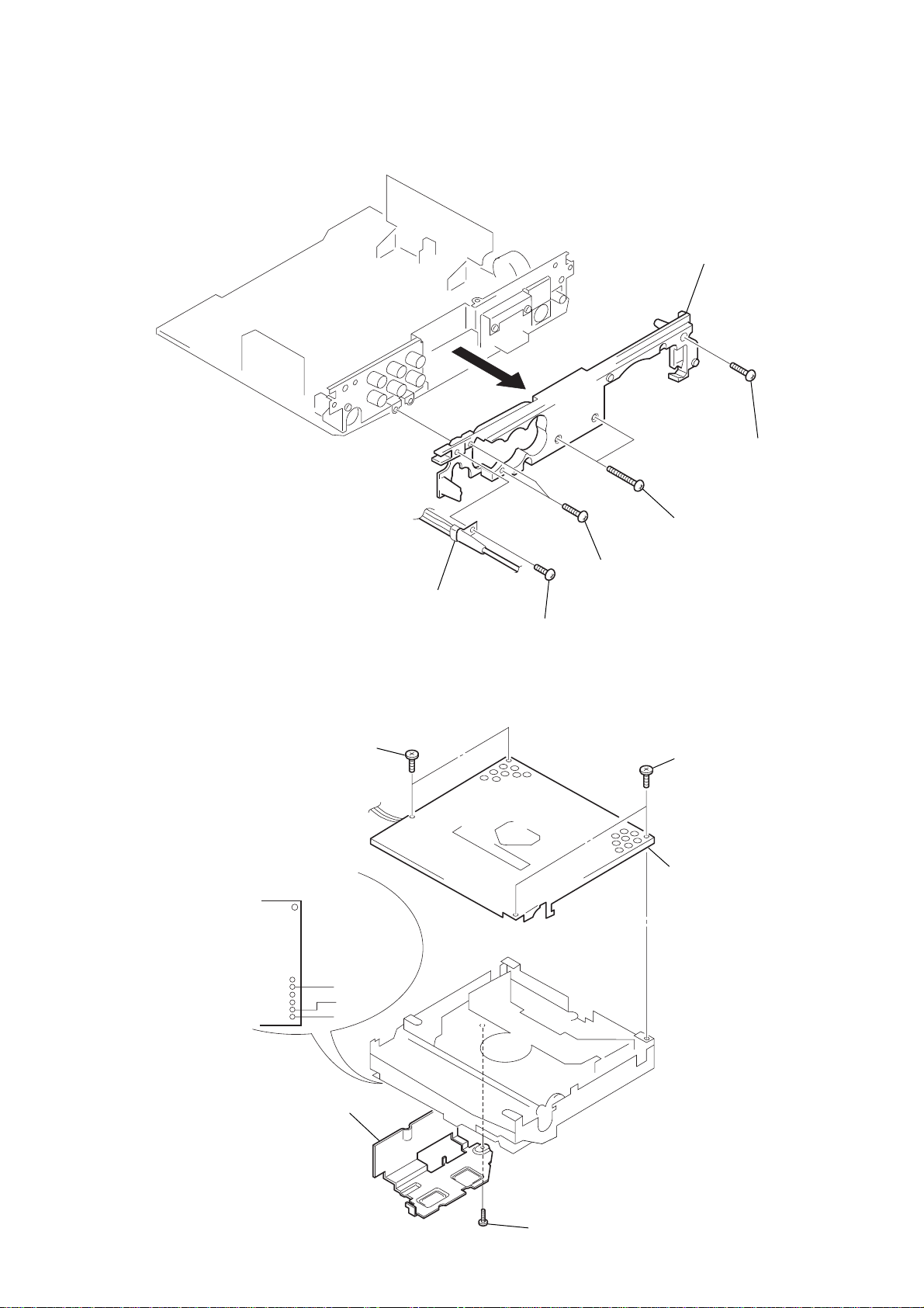
2-1. SUB PANEL ASSY
4
claws
2
PTT 2.6x6
6
sub panel assy
5
1
PTT 2.6x6
CN701
3
claw
7
Page 8
CDX-CA900/CA900X
4
4
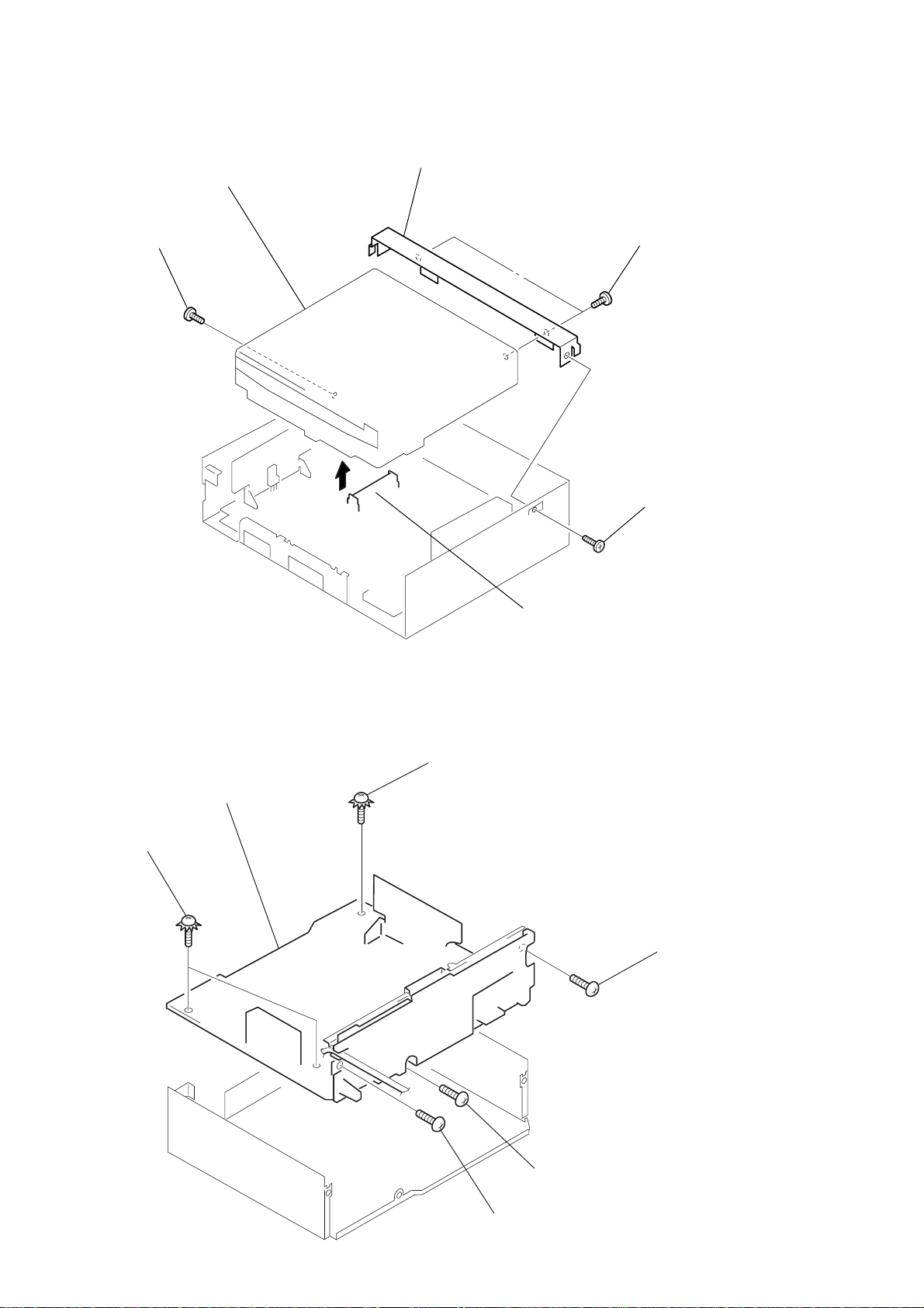
2-2. CD MECHANISM BLOCK
7
CD mechanism block
2
PTT 2.6x4
3
6
bracket (CD)
5
PTT 2.6x4
1
PTT 2.6x
2-3. MAIN BOARD
5
PTT 2.6x6
6
MAIN board
4
PTT 2.6x6
4
CN401
1
PTT 2.6x
2
PTT 2.6x4
3
PTT 2.6x4
8
Page 9
2-4. HEAT SINK
0
CDX-CA900/CA900X
6
heat sink
5
PTT 2.6x1
2-5. CHASSIS (T.U) ASSY
3
Unsolder the
lead wires.
4
P 2x3
2
PTT 2.6x4
1
PTT 2.6x4
3
PTT 2.6x10
4
PTT 2.6x16
5
P 2x3
6
chassis (T.U) assy
2
heat sink (MG393)
black
red
white
1
P 2x4
9
Page 10
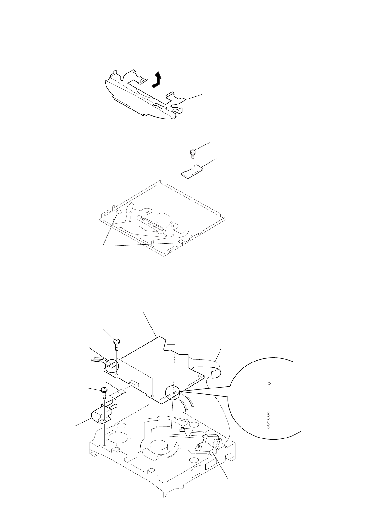
CDX-CA900/CA900X
2-6. DISC IN BOARD
4
guide (disc)
1
PS 2x3
2
DISC IN board
2-7. SERVO BOARD
2
Removal the solders.
4
5
loading motor assy
P 2x3
3
claws
6
PS 2x4
1
CN3
7
SERVO board
8
connector
3
Removal the solders.
BLU
BLU
10
optical pick-up block
Page 11
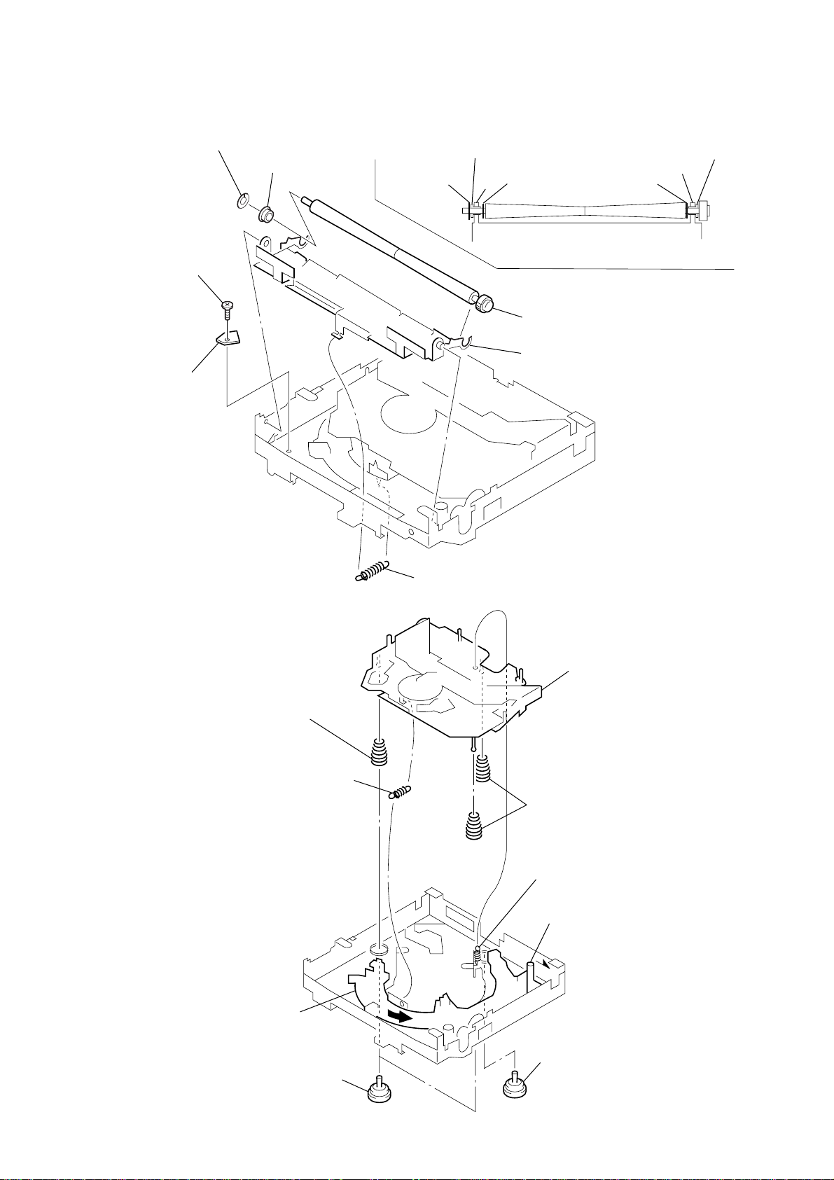
2-8. SHAFT ROLLER ASSY, LOAD BOARD
• When installing, take note of the positions
arm (roller) and washers. (Fig. 1)
3
retaing ring (roller)
4
bearing (roller)
6
PS 2x3
7
LOAD board
bearing (roller)
retaing ring (roller)
washer (RA)
arm
5
shaft roller assy
2
arm (roller T)
washer (RA)
Fig. 1
CDX-CA900/CA900X
bearing (roller)
arm
2-9. FLOATING BLOCK ASSY
8
compression spring (FL)
1
tension spring (KF1)
1
tension spring (RA3)
7
floating block assy
9
compression spring (FL)
2
tension spring (KR1)
5
Fit lever (D) in the
direction of the arrow.
6
Turn loading ring in the
direction of the arrow.
4
damper (T)
3
damper (T)
11
Page 12
CDX-CA900/CA900X
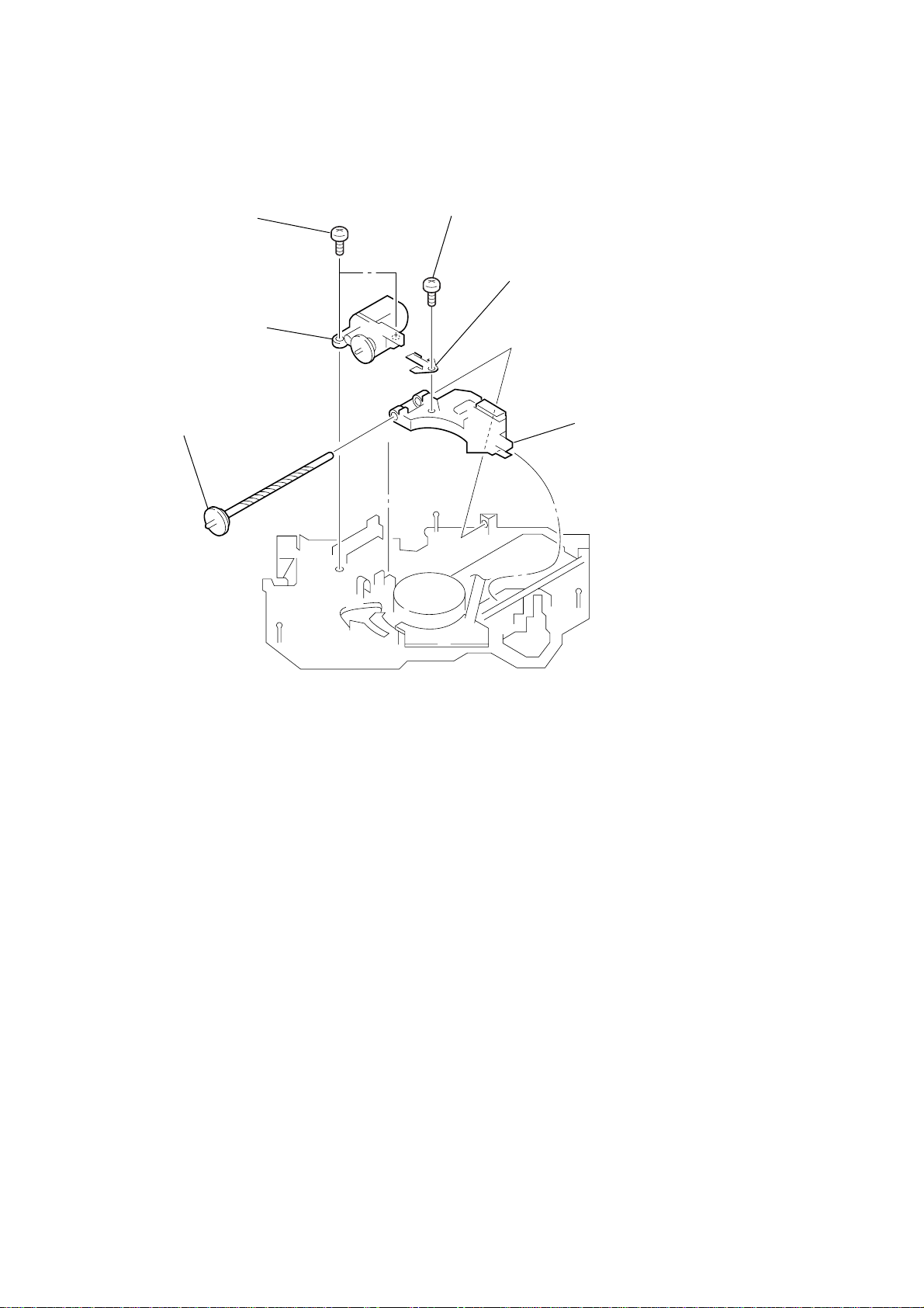
2-10. OPTICAL PICK-UP BLOCK
1
P 2x3
2
sled motor assy
6
shaft (feed) assy
4
P 2x3
5
leaf spring (feed)
3
optical pick-up block
12
Page 13
CDX-CA900/CA900X
SECTION 3
DIAGRAMS
3-1. IC PIN DESCRIPTIONS
• IC501 MB90574CPMT-G-367-BNDE1 (SYSTEM CONTROL) (US, Canadian Model)
• IC501 MB90574CPMT-G-368-BNDE1 (SYSTEM CONTROL) (E Model)
Pin No. Pin Name I/O Pin Description
1 RF OK I Servo IC RFOK signal input from servo IC (IC1)
2 CD RST O Servo IC reset signal output to servo IC (IC1)
3A0O
4 STB O Servo IC data storob signal output to servo IC (IC1) Data latch: “L”
5ATT O System mute control signal output
6XTAL EN O Not used in this set.
7 LIMIT I CD mechanism limit switch signal input (SW3)
8 VCC — Power supply pin (+5 V)
9 AMP ATT O Power amp mute signal output to power amp (IC381)
10 E2PSIO I/O EEPROM data signal input/output with tuner unit (TUX201)
11 E2PCKO O EEPROM clock signal output to tuner unit (TUX201)
12 DOOR SW/FLS SI I Front panel open/close detection signal input/Flash write data signal input
13 FLS SO O Flash write data signal output
14 BUS ON O Bus on control signal output
15 BEEP O Beep signal output to power amp (IC381)
16 (NCO) O Not used. (Open)
17 UNISI I SONY bus data signal input
18 UNISO O SONY bus data signal output
19 UNICKO O SONY bus clock signal output
20, 21 (NCO) O Not used. (Open)
22 SYSRST O System reset signal output to bus interface (IC601)
23 (NCO) O Not used.
24 SIRCS I Remote control data signal input
25 TSI I Servo IC serial data signal input from servo IC (IC1)
26 TSO O Servo IC serial data signal output to servo IC (IC1)
27 TCKO O Servo IC serial clock signal output to servo IC (IC1)
28 PH1 I CD mechanism PH1 detection signal input Not used in this set.
29 CD DSW I CD mechanism down switch signal input (SW4)
30 IN SW/PH2 I CD mechanism disc-in switch signal input (SW1)
31 PH3 I CD mechanism PH3 detection signal input Not used in this set.
32 CD LM LO O CD mechanism loading motor control signal output
33 VSS — Ground pin
34 C — Capacitance pin of power stabilized
35 CD LM EJ O CD mechanism eject motor control signal output
36 AMP ON O Amp on signal output to power amp (IC381) “L”: OFF, “H”: ON
37 VOLATT O Electronic volume mute signal output to electronic volume (IC301) “L”: Mute
38 DVCC — D/A converter VREF input (+5 V)
39 DVSS — D/A converter ground pin
40 ADSO1 O ADSO select switch output 1
41 ADSO2 O ADSO select switch output 2
42 AVCC — Analog power supply pin (+5 V)
43 AVRH — A/D convert Vref+ input (+5 V)
44 AVRL — A/D convert Vref– input (0 V)
45 AVSS — Analog ground pin
46 KEYIN0 I Key signal input
47 NC O Not used. (Open)
48 RC IN0 I Rotary commander signal input from remote in jack (J651)
49 (NCO) O Not used. (Open)
50 QUALITY I Tuner noise detection signal input (E model)
Servo IC command/parameter identification signal output to servo IC (IC1)
Command transmission: “L”
13
Page 14
CDX-CA900/CA900X
Pin No. Pin Name I/O Pin Description
51 NC O Not used. (Open)
52 MPTH O Not used in this set. (Open)
53 VSM I S-meter signal input from tuner unit (TUX201)
54 VCC — Power supply pin (+5 V)
55 BUS/AUX O BUS/AUX audio ground select signal output “H”: BUS
56 NS MASK O Tuner noise mask signal output (E model)
57 BOOT O Display microcomputer write control signal output to sub system control (IC701)
58 DOORIND O Front panel indicator signal output
59 to 62 — I Not used in this set. (Connect to ground.)
63 VSS — Ground pin
64 CD PACK I Servo IC CD text pack synchronization signal input
65, 66 (NCO) O Not used. (Open)
67 CD SELFSW I CD mechanism self load position detection switch signal input (SW2)
68 — O Not used. (Open)
69 FLASH W I Flash write mode detection signal input
70 I2CSIO O Tuner (TUX201), electronic volume (IC301) communication data signal output
71 I2CCKO O Tuner (TUX201), electronic volume (IC301) communication clock signal output
72 KEYACK I Key acknowledge detection signal input
73 X1A — Low speed oscillation signal input (32.768 kHz)
74 X0A — Low speed oscillation signal input (32.768 kHz)
75 DAVN I RDS data block synchronization detection signal input (E model)
76 (NCO) O Not used. (Open)
77 BU IN I Back up power detection signal input
78, 79 — O Not used. (Open)
80 ADON O Power control signal output of A/D converter
81 NOSESW I Front panel attachment detection signal input from nose detect switch (S102) “L”: ON
82 FLASH ON O Flash write jig power supply signal output
83 PWON O System power control signal output
84 — O Not used. (Open)
85 RAMBU I Reset detection signal input of RAM
86 HSTX I Hardware standby signal input “L”: Standby mode
87 MD2 I Operation mode signal input Connect to ground in this set.
88, 89 MD1, 0 I Operation mode signal input Connect to VCC in this set.
90 RESET I Microcomputer reset signal input
91 VSS — Ground pin
92 X0 — High speed oscillation signal input (3.68 MHz)
93 X1 — High speed oscillation signal input (3.68 MHz)
94 VCC — Power supply pin (+5 V)
95, 96 NC O Not used. (Open)
97 to 101 (NCO) O Not used. (Open)
102
103 10k/9k (P) I Not used. (Open) Destination detection signal input
104 (NCO) O Not used. (Open)
105 CD MON O CD mechanism power control signal output to power supply (IC801)
106 CD ON O CD mechanism voltage control signal output to power supply (IC801)
107 RCIN1 (P) I Rotary commander signal input from remote in jack (J651)
108 TESTIN (P) I Test mode set up detection signal input
109 TELATT (P) I Tell mute detection signal input
110 ILLIN (P) I Illumination line detection signal input “L”: Dimmer on
111 — O Not used. (Open)
112 (NCO) O Not used. (Open)
113 TUNON O Tuner on signal output
MODELSEL0
U•E/J (P)
I Not used. (Open) Destination detection signal input
14
Page 15

CDX-CA900/CA900X
Pin No. Pin Name I/O Pin Description
114 to 116 — O Not used. (Open)
117 ACCIN I ACC power detection signal input “L”: ACC on
118 — O Not used. (Open)
119 VSS — Ground pin
120 CD TSTB O Servo IC CD text parameter storob signal output to servo IC (IC1)
15
Page 16

CDX-CA900/CA900X
• IC701 HD64F2398A04FWV (SUB SYSTEM CONTROL)
Pin No. Pin Name I/O Pin Description
1PG3 O Spectrum analyzer data clock signal output to electronic volume (IC301)
2PG4 O Not used. (Open)
3 VSS — Ground pin
4NC—Not used. (Open)
5 VCC — Power supply pin (+5 V)
6 to 9 PC0 to PC3 O Not used. (Open)
10 VSS — Ground pin
11 to 14 PC4 to PC7 O Not used. (Open)
15 to 18 PB0 to PB3 O Not used. (Open)
19 VSS — Ground pin
20 to 23 PB4 to PB7 O Not used. (Open)
24 to 27 PA0 to PA3 O Not used. (Open)
28 VSS — Ground pin
29 to 32 PA4/IRQ4 to PA7/IRQ7 O Not used. (Open)
33 SA EN I Spectrum analyzer enable signal input from system control (IC501)
34 BU IN I Back up power signal input from bus interface (IC601)
35, 36 VSS — Ground pin
37 P65/IRQ1 O Not used. (Open)
38 BUS ON I Bus on signal input from system control (IC501)
39 VCC — Power supply pin (+5 V)
40 to 43 PE0 to PE3 O Not used. (Open)
44 VSS — Ground pin
45 to 48 PE4 to PE7 O Not used. (Open)
49 — O Not used. (Open)
50 LINK OFF O Link off signal output
51 PD2 O Not used. (Open)
52 ILL ON O Illumination power control signal output
53 VSS — Ground pin
54, 55 — O Not used. (Open)
56 PD6 O Not used. (Open)
57 BOOT I Flash write mode detection signal input from system control (IC501)
58 VCC — Power supply pin (+5 V)
59 NC O Not used. (Open)
60 TX/LCD DATA O Flash write data signal output/LCD driver data signal output
61 SP SI O Not used. (Open)
62 RX/DOOR SW I Flash write data signal input/Door switch detection signal input
63 L RST O Reset signal output
64 LCD SCK O LCD driver clock signal output
65 VSS — Ground pin
66 LCD CEI O LCD driver chip enable signal output
67, 68 VSS — Ground pin
69 to 71 (NCO) O Not used. (Open)
72 to 79 P27 to P20 O Not used. (Open)
80 VCL — Connect to external capacitor
81 RST I Reset signal input
82 NMI I Non-maskable interruption signal input
83 STBY (H) — Standby mode pin
84 VCC — Power supply pin (+5 V)
85 XTAL — Crystal oscillator connection pin (18.432 MHz)
86 EXTAL — Crystal oscillator connection pin (18.432 MHz)
87 VSS — Ground pin
88 PF7 O Not used. (Open)
16
Page 17

CDX-CA900/CA900X
Pin No. Pin Name I/O Pin Description
89 VCC — Power supply pin (+5 V)
90 PF6 OPEN — Not used. (Open)
91 to 96 PF5 to PF0 O Not used. (Open)
97 UNI SO O SONY bus data signal output
98 UNI SI I SONY bus data signal input
99, 100 VSS — Ground pin
101 UNI SCK I SONY bus clock signal input
102 NCO O Not used. (Open)
103 AVCC — Power supply pin for A/D, D/A converter
104 VREF — Reference voltage input for A/D, D/A converter
105 to 110 A40/AN0 to A45/AN5 I Not used. (Connect to ground in this set.)
111 P46/AN6/DA0 I Not used. (Connect to ground in this set.)
112 P47/AN7/DA1 I Spectrum analyzer data signal input from electronic volume (IC301)
113 AVSS — Ground pin for A/D, D/A converter
114 VSS — Ground pin
115 to 122 P17 to P10 O Not used. (Open)
123 to 125 MD0 to MD2 — Mode pin
126 to 128 PG0 to PG2 O Not used. (Open)
17
Page 18

CDX-CA900/CA900X
)
3-2. CIRCUIT BOARDS LOCATION
SUB (CD) board
• Waveforms
— Servo Board —
(MODE: CD PLAY)
LOAD board
KEY board
DISC IN board
— Main Board —
SUB board
LIMIT board
tuner unit
(TUX201
MAIN board
SERVO board
— Key Board —
1
2
3
4
5
16.9344MHz
IC1
IC1
IC1
IC1
(XTAL)
wd
3.3msec
(PACK)
ts
(RFO)
uj
Approx. 100mVp-p
(FEO)
oa
1.8Vp-p
5Vp-p
1.5Vp-p
0V
1
2
3
4
IC201
IC501
IC501
IC701
4.332MHz
(OSC O)
4
32.768kHz
(XOA)
uf
3.68MHz
(XO)
os
18.432MHz
(EXTAL)
ih
2.2Vp-p
4.5Vp-p
3.8Vp-p
1.4Vp-p
1
IC903
4MHz
(XOUT)
4
4.6Vp-p
18
Approx. 100mVp-p
od
(TEO)
IC1
0V
Page 19

3-3. BLOCK DIAGRAM — CD SECTION —
OPTICAL PICK-UP
KSS-720A
RF AMP,DIGITAL SERVO
DIGITAL SIGNAL PROCESSOR
IC1
CDX-CA900/CA900X
PD
LD
A
C
B
D
E
F
FOCUS
COIL
I-V
CONV.
LD
DRIVE
Q1
A
84
C
85
B
82
D
83
E
87
F
86
PD
97
A+5V
LD
98
FOCUS/TRACKING COIL DRIVE,
SLED/SPINDLE/LOADING MOTOR DRIVE
FCS-
15
FCS+
16
APC
IC2
FOCUS
COIL
DRIVE
TRACKING
ERROR
(Page 20)
TUNER
LOUT
RF
EQ
FORCUS
ERROR
FD
26
EFM
DEMOD
SERVO
CTL
FDTDSD
62 63 64 65
MD
D/A
CONV
DSUB CODE
PROCESS
I/F
OSC
23 24
X1
16.9344MHz
ROUT
PACK
TSTB
TSCK
TSI
SCK
STB
RST
RFOK
16
12
R-CH
52
56
55
54
SI
8
SO
7
6
5
AO
4
3
2
SW4
(DOWN)
CDL
SECTION
A
SYSTEM CONTROL
64
CD_PACK
120
TSTB
26
CD_TSO
25
CD TSI
27
CD TCK
4
STB
3
AO
2
CD_RST
1
RFOK
29
D SW
IC501 (1/3)
TRACKING
COIL
• Signal path
:CD
• R-ch is omitted due to
same as L-ch.
M902
(SLED)
M901
(SPINDLE)
M903
(LOADING)
67
30
32
35
105
106
7
SELFSW
IN/PH2
LIMIT
LOAD
EJECT
CDM ON
CD ON
VCC
SW2
(SELF)
SW1
(DISC IN)
SW3
(LIMIT)
6
Q405
BATT
TRK+
17
TRK-
18
SL-
M
13
SL+
14
SP-
M
11
SP+
12
LD-
M
9
LD+
10
TRACKING
COIL
DRIVE
SLED
MOTOR
DRIVE
SPINDLE
MOTOR
DRIVE
LOADING
MOTOR
DRIVE
TD
23
SD
5
MD
6
LOAD
1
EJECT
2
A+5V
AU+5V
D+5V
DR+6V
BU+5V
7
3
5
1 2
SW5V
SW6V
5V
POWER SUPPLY
IC801
19 19
Page 20

CDX-CA900/CA900X
3-4. BLOCK DIAGRAM — TUNER SECTION —
CN201
(ANTENNA)
1
2
ANT AM
ANT FM
(Page 19)
(Page 21)
TUNER UNIT
TUX201
SECTION
DISPLAY
SECTION
MPX
AMDET
RDS
S METER VSM
SDA
SCL
SDA
EEPROM
SCL
CD
CN302
–1
CN301
CN101
–2
–5
–6
–3
–4
1
9
2
10
4
12
3
11
13
14
7
15
5
6
19
17
18
16
L
BUS AUDIO IN
R
L
R
L
R
L
R
FL+
FL–
RL+
RL–
FR+
FR–
RR+
RR–
TEL MUTE
ILL
ACC
TEST
AMP REM
ANT REM
B+
F901
B+
AUDIO OUT
FRONT
AUDIO OUT
REAR
SUB OUT
ELECTRONIC VOLUME
IC301
4
AUXL
IC304 (2/2)
1
43
MDL
21
SACLK
23
SA OUT
38
AC OUTL
33
AC INL
12
MPX1
9
AM
14
MP IN
13
LEVEL
19
SDA
20
SCL
17
SM
SYSTEM CONTROL
IC501 (2/3)
37
VOL ATT
50
QUALITY
56
NS MASK
53
I2CSIO
70
I2CCKO
71
E2PSIO
10
E2PCKO
11
OUT LF
OUT LR
OUT SW
ADSO1
ADSO2
BUS/AUX
ATT
AMP ATT
AMP ON
BEEP
TEL ATT
ILL IN
ACC IN
X1A
X0A
TEST IN
PW ON
TUN ON
28
27
24
MUTE
CONTROL
Q843,844
40
41
55
5
9
36
15
109
110
117
73
74
108
83
92
X0
93
X1
113
X501
32.768kHz
X502
3.68MHz
TU +8.5V
ACC CHECK
AUDIO+8.5V
Q101
POWER
CONT
Q201,202
ILLUM CHECK
Q102
POWER
CONT
Q801-803
AUDIO+8.5V
Q103
BATT
CDL
A
SACLK
B
SAOUT
IC304 (1/2)
ADSO SWITCH
76
IC201
SDA
SCL
IC361
Q211
9
10
10
8
E MODEL
FM AMP
Q212
NOISE
CANCEL
IC202
RDS DECODER
9
X201
4.332MHz
14
12
13
17
18
16
4
5
FM DET
XO
XI
3
257
• Signal path
GND SWITCH
BATT
BATT
Q391
Q306
Q308
Q310
FL
12
RL
11
22
4
16
POWER
CONT
Q104,105
POWER
CONT
Q106,107
POWER AMP
IC381
MUTE
STBY
AC-GND
R-CH
R-CH
R-CH
5
3
9
7
R-CH
BATT
: FM
: AM/MW
: CD
TU +5V
+5V REG
Q203
TU+8.5V
• R-ch is omitted due to
same as L-ch.
2020
Page 21

3-5. BLOCK DIAGRAM — DISPLAY SECTION —
CDX-CA900/CA900X
CN601
(BUS CONTROL IN)
8
3
6
2
5
1
4
7
BATT
BUS ON
SW
Q603
BATT
BATT
DATA
CLK
6
4
3
LCD
LCD901
BUS INTERFACE
IC601
BUS
ON
RESET
BATT(L)
CHECK
BATT
CHECK(H)
Q602
11
121
132
10
8
9
LCD DRIVER
IC901
DIMMER
106
CLK
DATA
SUB SYSTEM CONTROL
IC701
RST
SA CLK
SA IN
BOOT
LCD SO/TX
ILL ON
63
112
57
62
60
52
SA CLK
1
SA OUT
B
BU +5V
E MODEL
J651
(REMOTE IN)
TUNER
SECTION
(Page 20)
AD ON
CONTROL
Q701
KEY IN
MATRIX
98
UNI SI
97
UNI SO
UNI SCK
101
BUS ON
38
BU IN
34
BUF
IC702
X701
18.432MHz
118
CE
120
RST
76
81
LINK OFF
50
XTAL
85
EXTAL
86
DOOR SW/RX
SCK
64119
LCD
CEL
66
SYSTEM CONTROL
17
UNI SI
18
UNI SO
19
UNI CKO
14
BUS ON
77
BU IN
22
SYSRST
72
KEY ACK
AD ON
80
107
RC IN1
48
RC IN0
46
KEY IN0
57
BOOT
12
FLS SI
13
FLS SO
IC501 (3/3)
SIRCS
HSTX
RSTX
SIRCS CONTROL
IC903
24
86
90
17 9
S101
RESET
OUT
XIN XOUT
3 4
RESET
X910
4MHz
6
1 3
IC502
RESET
716
LED900IC902
BU +5V
DIMMER
CONTROL
Q901
POWER
CONTL
Q702,703
POWER
CONT
Q705,706
BATT
BATT
S102
(NOSE)
81
58
NOSE DET
DOOR IND
21 21
Page 22

CDX-CA900/CA900X
3-6. PRINTED WIRING BOARDS — CD MECHANISM SECTION — • Refer to page 18 for Circuit Boards Location.
THIS NOTE IS COMMON FOR PRINTED WIRING
BOARDS AND SCHEMATIC DIAGRAMS.
(In addition to this, the necessary note is
printed in each block.)
for schematic diagram:
• All capacitors are in µF unless otherwise noted. pF: µµF
50 WV or less are not indicated except for electrolytics
and tantalums.
• All resistors are in Ω and 1/
specified.
•%: indicates tolerance.
f
•
• C : panel designation.
Note:
The components identified by mark 0 or dotted
line with mark 0 are criti-
cal for safety.
Replace only with part
number specified.
• A : B+ Line.
• Power voltage is dc 14.4V and fed with regulated dc power
•Voltages are taken with a VOM (Input impedance 10 MΩ).
•Waveforms are taken with a oscilloscope.
• Circled numbers refer to waveforms.
• Signal path.
• Abbreviation
: internal component.
supply from ACC and BATT cords.
Voltage variations may be noted due to normal produc-
tion tolerances.
Voltage variations may be noted due to normal production tolerances.
F : FM
f : AM/MW/LW
J : CD
CND : Canadian model.
4
W or less unless otherwise
Note:
Les composants identifiés par
une marque 0 sont critiques
pour la sécurité.
Ne les remplacer que par une
piéce portant le numéro
spécifié.
234567891011121314
1
A
B
C
D
E
F
for printed wiring boards:
• X : parts extracted from the component side.
• Y : parts extracted from the conductor side.
• x : parts mounted on the conductor side.
a
•
• : Pattern from the side which enables seeing.
Caution:
Pattern face side: Parts on the pattern face side seen from the
(Side B) pattern face are indicated.
Parts face side: Parts on the parts face side seen from the
(Side A) parts face are indicated.
• Abbreviation
: Through hole.
(The other layer’s patterns are not indicated.)
CND : Canadian model.
G
H
I
J
2222
Page 23

CDX-CA900/CA900X
A
B
C
D
E
1
234567891011 12 13 14
• Semiconductor
Location
Ref. No. Location
IC1 E-7
IC2 H-7
Q1 C-6
TP66
TP64
TP47
R21
TP48
R22
TP74
TP50
TP56
TP76
C71
TP51
TP52
TP58
TP61
TP62
CN1
TP7
TP72
TP80
TP60
TP59
TP71
TP63
R26
R19
TP77
C4
R17
TP9
TP8
TP78
TP70
C27
CN2
C5
C1
R30
Q1
C3
R29
C43
R3
C6
R18
C25
C41
C34
TP11
TP79
C9
C10
C8
C16
C17
C29
TP12
C70
C15
IC1
TP82
TP81
C11
TP83
C14
R5
C13
C18
TP89
R9
C24
TP23
TP84
TP10
C19
TP88
(Page 31)
C20
C23
R8
TP22
TP24
TP25
F
G
H
TP20
X1
C36
TP92
R7
R6
C22
TP16
TP17
TP34
TP35
TP36
TP46
C38
IC2
TP39
BP2
BP1
TP37
TP38
TP30
TP41
TP40
TP45
TP42
TP31
TP27
R12
R10
C30
TP44
TP43
R15
TP26
TP28
C35
TP29
TP33
TP32
TP15
BP3
TP5
TP4
TP6
TP3
TP2
R14
TP14
BP4
TP18
TP21
TP1
TP75
TP69
TP57
TP73
TP53
TP86
TP87
R20
TP68
FB5
C44
TP49
C26
R31
TP85
TP55
TP91
TP90
TP19
I
TP54
CN3
+- +-
J
23 23
Page 24

CDX-CA900/CA900X
• Refer to page 18 for Waveforms.
3-7. SCHEMATIC DIAGRAM — CD MECHANISM SECTION — • Refer to page 34 for IC Block Diagrams.
CN2
SW3
TP77
TP78
C1 C5
TP81
TP82
TP83
TP84
R29
R30
TP79
TP80
C43
Q1
C3
TP9 TP8
R26
R3
C4
TP7
C6
C14
TP10
C13
C11
R5
C15
C10
C9
TP12
TP11
TP89
C18
C19
C20 C23
R9
C24
TP24
TP22
TP25
TP23
R8
IC1
TP88
C35
TP45
TP44
TP43
TP42
TP41
TP40
TP39
TP38
TP37
TP46
TP36
C38
CN1
M902
M901
SW4
SW2
SW1
Note:
•Voltage is dc with respect to
ground under no-signal conditions.
no mark : CD PLAY
CN3
TP1
TP4
TP5
TP2
TP3
M903
TP93
TP94
TP95
TP96
TP97
TP98
TP92
TP85
TP87
TP86
C8
TP35
TP34
C16C70
IC B/D
C17
C41
C27
C26
R12
R10
C30
TP31
BP1
TP30
R15
R14
TP90
TP91
TP27
TP29
TP26
TP28
R7
TP15
TP21
BP3
TP14
BP4
R6
TP18
TP17
TP20
TP16
TP19
C22
IC2
C29
C25
C34
X1
C71
TP33
BP2
TP32
C36
R31
C44
FB5
R21
R22
R18
R19
R20
R17
TP66
TP61
TP76
TP60
TP75
TP59
TP74
TP58
TP73
TP57
TP72
TP56
TP71
TP55
TP70
TP54
TP69
TP53
TP68
TP52
TP51
TP50
TP64
TP49
TP48
TP63
TP47
TP62
CN1
(Page 27)
IC B/D
2424
Page 25

• Refer to page 18 for Waveform.
3-8. SCHEMATIC DIAGRAM — MAIN SECTION (1/4) — • Refer to page 34 for IC Block Diagrams.
CDX-CA900/CA900X
Q212
CN201
C217
R223
R222
X201
C237
C232
C236
R233
C235
IC201
C231
C234
C233
R236
C218
R226
R227
C220
R231
R232
C241
FB231
C221 R228 R229
C201
C222
C229
C230
C202
R201
C223
FB230
IC202
IC B/D
D204
C224
TUX201
FB201
Q203 Q201
R205
C227
D202
C226
D203
R225
R224
R207
C225
Q211
R208
R202
C205
C206
R203
Q202
R251
C251
R301
R302
C313
C309
C306 C308
C254 C255
R252
C252 C253
R253
C312
C307
C321
R303
IC B/D
R304
R362
C318
C317
C311
R254
C304
C362
R361
R363
IC304
C310
C303
C316
IC361
IC301
C361
D300
R370
R365
R364
C394
C302
C305
R309
C319
R366
R305
C320
C393
C314
R306
C315
R371
R372
R373
R374
R375
R307
C375
C374
R308
C373
C372
IC305
C363
C322
(Page 26)
C371
C219
R230
(Page 27)
25 25
(Page 28)
Note:
•Voltage is dc with respect to ground under
no-signal (detuned) condition.
no mark : FM
(): AM/MW/LW
Page 26

CDX-CA900/CA900X
3-9. SCHEMATIC DIAGRAM — MAIN SECTION (2/4) —
(Page 25)
C802
C803
R805
D801
R804
R803
Q801
Q803
Q802
R802
C801
R801
Q405
R806
C804
C807
C806
IC801
D802
C335
C337
C339
C341
C343
C808
C805
Q306
Q307
Q308
Q309
Q310
C842
Q843
R399
Q844
R845
R332
R333
R336
R338
R340
R342
R344
C843
R331
R334
R330
D845
R847
Q391
R849
C336
C338
C340
C342
R383
R384
R386
R385
R848
R398
D391
IC381
C844
C386
C387
C388
C389
C382
C383
C384
C385
C345
C344
R840
C847
R850
C848
C378
CN302
C390
C346
C347
CN301
C380C381
D301
D302
D303
D304
D305
D306
D307
D308
(Page 27)
Q103
R113
R114
R125
Q102
D105
R110
R111
C103
(Page 28)
Q101
R105
C102
R106 R107
TH101
C111
C112
R108 R109
D106
R115
R119 R120
Q105
C110
TH102
C115
2626
C114
CN101
C109
R103
R118
R117
C108
R102
R132
R104
D101
L101
R130
R101
R131
F901
D107
Q107Q104
C113
R116
Q106
D102
Note:
•Voltage is dc with respect to ground under
no-signal (detuned) condition.
no mark : FM
(): AM/MW/LW
<>: CD PLAY
Page 27

• Refer to page 18 for Waveforms.
3-10. SCHEMATIC DIAGRAM — MAIN SECTION (3/4) — • Refer to page 36 for IC Block Diagram.
CDX-CA900/CA900X
(Page26)(Page 25)
CN601
L401
C401
C410
R407
C408
C407
R410
FB400
FB401
C403
R601
TH601
C604
R605
R607
CN401
D606
C603
D605
J651
(Page 24)
Q603
D610
D609
D604
R654
Q602
C601
IC601
C400
R652
R411
R412
D603
R409
C406
IC B/D
C602
R604
R653
FB402
D601
D607
D653
R506
C505
D654
D505
R536
C506
R545
C503
C514
C504
R548
R549
R505
R507
C507
508
R
C508
R509
R534
R510
R535
C509
IC501
C510
R533
X501
R532
R544
C511
R504
R531
R511
R530
R512
R514
R528
R538
R539
R537
C512
R501
R540
S102
R541
R542
C501
C513
S101
R525
R543
D504
R522
R523
C523
C522
FB501
C521
R516
R527
(Page 28)
X502
R571
IC502
R524
Q701
D501
Note:
•Voltage is dc with respect to ground under
no-signal (detuned) condition.
no mark : FM
(): AM/MW/LW
<>: CD PLAY
27 27
Page 28

CDX-CA900/CA900X
3-11. SCHEMATIC DIAGRAM — MAIN SECTION (4/4) — • Refer to page 18 for Waveform.
(Page 25) (Page 26)
(Page 27)
FB701
C520
C709 C708
R712
R521
C706
FB702
C705
C707
C711
R734
C710
C727
R706
R702
R709
R707
R708
C703
Q702
R724
R737 R738
Q703
Q705
R728
R739 R740
Q706
C704
IC701
C702
C726C715
R703
X701
R704
R705
R713
R732
FB703
C712
D703
R744
R717
C716
IC702
R746
R745 R748 R749
C722
R733 R711
R741
C714
CN701
CN851
LED851
LSW851(1/2)
LSW851(2/2)
R855 R856
D852
(Page 33)
D851
CN852
Note:
R720
R716
R714
C717
C701C718
D708
•Voltage is dc with respect to ground under
no-signal (detuned) condition.
no mark : FM
2828
Page 29

3-12. PRINTED WIRING BOARD — RELAY SECTION — • Refer to page 18 for Circuit Boards Location.
CDX-CA900/CA900X
A
B
C
D
1
LSW851
234567891011 12 13 14
LED851
R855
R856
E
F
G
H
D852
D851
(Page 31)
CN851
1
CN852
814
7
I
• Semiconductor
Location
Ref. No. Location
D851 F-12
D852 F-11
LED851 B-8
(Page 32)
29 29
Page 30

CDX-CA900/CA900X
3-13. PRINTED WIRING BOARD — MAIN SECTION — • Refer to page 18 for Circuit Boards Location.
• Semiconductor Location
Ref. No. Location
(D101) D-9
D102 C-9
D105 C-7
(D106) D-7
(D107) D-7
D202 E-2
D203 E-2
D204 F-3
(D300) D-3
(D301) C-8
(D302) C-8
(D303) C-8
(D304) D-8
(D305) D-8
(D306) C-8
(D307) D-8
(D308) D-8
D391 C-3
D501 H-7
D504 H-7
(D505) H-5
(D601) H-7
D603 E-8
D604 C-9
D605 C-9
(D606) C-9
D607 I-4
D609 D-9
D610 E-9
D653 I-7
D654 I-7
(D703) I-2
(D708) I-3
D801 H-9
D802 G-9
D845 D-6
IC201 H-2
IC202 G-3
(IC301) D-4
IC304 D-3
( ): SIDE B
Ref. No. Location
IC305 E-3
IC361 E-3
(IC381) B-6
(IC501) H-6
IC502 H-7
IC601 D-9
(IC701) H-4
IC702 I-4
(IC801) G-10
Q101 C-8
Q102 C-8
Q103 C-7
Q104 D-8
Q105 E-8
Q106 E-8
Q107 E-8
Q201 E-2
Q202 D-2
Q203 E-2
Q211 G-3
Q212 G-3
Q306 C-4
Q307 C-4
Q308 C-3
Q309 C-3
Q310 D-2
Q391 C-3
Q405 H-9
Q602 D-9
Q603 D-9
Q701 I-7
(Q702) I-8
Q703 I-8
(Q705) I-9
Q706 I-9
(Q801) H-9
Q802 G-9
Q803 G-9
Q843 D-6
Q844 D-6
C804
C806
R806
D604
D605
R601
Q405
C801
Q802
R801
Q603
IC601
D802
R803
R802
R605
R107
C602
Q803
D102
C109
D609
R804
Q706
R739
C102
R607
Q602
D610
D801
R728
R130
R101
C603
R740
R117
R118
R805
C802
Q703
R105
D603
R604
R738
R102
R132
C601
C110
R115
C113
R724
R106
R116
Q106
R737
Q101
R104
Q104
Q107
R712
Q102
R120
Q105
C111
C114
R110
R109
R111
C112
C115
R119
R108
R527
R524
Q701
D653
D654
D105
Q103
R131
R103
R114
R113
R125
IC502
R525
R407
R537
R543
R571
R510
R850
D504
D501
C512
R840
R522
R410
C513
R511
C847
R516
C511
R512
R847
R849
R540
X502
R848
R504
C501
Q844
Q843
R409
R539
R532
R383
D845
R501
C382
C842
R845
R533
C503
C386
R548
R544
R549
R535
R534
C504
C506
R542
C384
C388
C508
C507
R508
R509
R507
R385
C389
R309
R411
R412
R541
R538
R528
R530
R531
R505
R386
C385
R545
C387
R384
C383
C253
R506
D607
FB201
C255
C307
R253
C252
FB701
C704
C703
R705
C338
Q307
C254
R251
C702
X701
C710
R338
R304
R361
R362
R363
C251
C394
C393
R303
R308
R252
C716
R704
C715
IC702
R307
C336
Q306
C318
C317
C322
C224
R225
R702
R336
C321
IC361
C320
C363
IC305
R703
C727
C362
R224
Q212
R711
C361
D204
Q211
C726
R733
Q309
C319
R223
R222
C711
C342
R342
C223
C218
C722
R741
IC304
R365
R306
C315
C229
R301
R302
R305
C222
IC202
C217
C219
C340
R330
C313
R229
C705
C706
R744
R366
R364
R230
R228
C221
R521
R713
R340
Q308
C390
D203
D202
C220
Q391
D391
R398
Q310
Q202
C226
C235
C236
C237
R202
Q201
R227
R226
R334
R207
C234
R203
R205
R208
R231
234567891011121314
R333
R332
R399
Q203
R331
IC201
R748
R749
R232
R745
R746
R233
FB230
C233
R236
C231
C232
C241
1
X201
A
B
C
D
E
F
G
H
I
J
3030
Page 31

CDX-CA900/CA900X
A
B
C
D
E
F
1
CN201
TUX201
C201
234567891011 12 13 14
CN302
J651
C202
C205
C206
C225
R201
C227
CN301
C309
C308
C344
R344
C306
C345
C378
C314
C343
C312
C339
C346
R370
C341
D300
C310
C347
C311
C335
C316
IC301
C337
R254
C371
R371
C303
C304
C372
R372
C848
C373
R373
C374
R374
C302
C375
R375
C305
C400
C380
FB402
C406
IC381
C803
C381
C844
CN401
FB401
C410
C843
C103
TH101
D106
TH102
D107
FB400
C401
C408
C407
C403
FB501
L401
CN101
F901
D306
D301
D302
D303
D304
D308
D305
D307
C108
D101
CN601
D606
TH601
C808
C805
R654
L101
C604
R652
R653
(Page 23)
BATT
US,Canadian model
E model
G
H
J
IC701
C708
R707
R706
C709
R709
FMB4
R708
R720
R717
C520
D505
C505
C514
R536
C509
IC501
X501
C510
C230
FB231
R732
C717
C718
R714
R734
FMB5
C712
I
D703
C701
CN701
C714
R716
FB703
C707
D708
FB702
C521
C522
R523
R514
C523
FMB3
D601
Q702
S102
Q801
Q705
C807
IC801
S101
(Page 29)
31 31
Page 32

CDX-CA900/CA900X
3-14. PRINTED WIRING BOARD — KEY SECTION — • Refer to page 18 for Circuit Boards Location.
A
B
C
D
1
C905
LSW922
234567891011 12 13 14
LSW923
R922
R921
R923
R924
LSW924
LED911
LED910
LCD901
LED912
LED913
LED914
LED915
C902
R934
LSW921
E
F
G
H
C908
R903
IC902
C906
R902
C907
C909
LED900
C904
R933
FB901
R919
R918
R972
IC903
C912
R911
C910
R973
R917
R916
R915
R914
R910
FB902
R971
R912
X910
C911
R913
D910
• Semiconductor Location
Ref. No. Location
D900 H-12
D901 H-12
D902 F-11
D910 F-4
D920 F-14
D972 G-10
D974 G-11
Ref. No. Location
LED900 H-1
LED910 C-3
LED911 B-3
LED912 C-3
LED913 B-13
LED914 C-13
LED915 C-13
FMB3
IC901
FMB4
R994
R993
R992
R991
R988
R987
C983
C993
C991
C986
C992
R982
R983
C982
D972
R981
R986
R985
R984
R990
D974
D902
C990
R976
D901
C901
R974
R975
R980
R979
CN901
D900
(Page 29)
Q901
D920
C900
R901
R904
IC901 F-8
IC902 G-1
IC903 G-3
Q901 F-13
3232
Page 33

3-15. SCHEMATIC DIAGRAM — KEY SECTION — • Refer to page 18 for Waveform.
C908
R902
C907
C906
R903
R919
CDX-CA900/CA900X
R918
(Page 28)
CN901
C901
D901
D902
R904
D900
R901
IC902
LED900
D920
LSW921(2/2)
LSW922(2/2)
LSW923(2/2)
LSW924(2/2)
C900
C902
FB901
R921
R922
R923
R924
C905
C904
C909
IC903
C910
FB902
C911
R933
LSW922(1/2)
LED910
LSW923(1/2)
LSW924(1/2)
LSW921(1/2) Q901
LED911
R972
R979
R911
R912
C912
X910
LED912
LED913
R974
R910
R914
R913
D910
R975R973R971
R976
R915
R916
LED914
LED915
R917
R981
R982
R988
C982
D972
R990
IC901
D974
R983
R991
C990
C986
C983R987
C991
C992
C993
R984
R985
R986
R992
R993
R994
R934
R980
LCD901
Note:
•Voltage is dc with respect to ground under no-signal
(detuned) condition.
no mark : FM
33 33
Page 34

CDX-CA900/CA900X
• IC BLOCK DIAGRAMS
IC1 µPD63711GC-8EU
AGCO74RFI73C3T72ASY71EFM70AVDD697E DAC3687D DAC2677C DAC1667F DAC065MD64SD63TD62FD
75
AGCI
76
RFO
77
EQ2
78
EQ1
79
RF-
80
AGND
81
A
82
C
83
B
84
D
AVDD
REFOUT
FEO
TE-
TEO
TE2
TEC
AGND
AVDD
85
F
86
E
87
88
89
FE-
90
91
92
93
94
95
96
PD
97
LD
98
99
PN
100
AMP BLOCK
DEFECT
MIRR
EFM
COMPARATOR
EFM
FEOFS
TEOFS
RF
EFM
SWITCH
FOK
A3T
FEO
TEO
COMPARATOR
MICROCOMPUTER INTERFACE
AUTO GAIN
CONTROLLER
SVDRAM
PROCESSOR
DEFECT
COMPARATOR
RFENV
MIRENV
TRACKING
A/D CONVERTER
REGISTER
FOCUS
REGISTER
ADDER
MULTIPLIER
SVROM
CLV
D/A
FD/TD/SD/MD
CONTROLLER
SVCRAM
ROM
DECODER
ATEST59TEST158TEST057DGND56TSTB55TSCK54TSI53TSO52PACK51DVDD
AGND
60
61
MICROCOMPUTER INTERFACE
CD-TEXT DECODER
MEMORY
PROCESSOR
16K
SRAM
SUB-CODE PROCESSOR
EFM DEMODULATOR
TIMING GENERATOR
D/A
INTERFACE
CIRCUIT
DE-EMPHASIS CIRCUIT
OCTUPLED
OVERSAMPLING DIGITAL FILTER
NOISE SHAVER
OUTPUT BUFFER
SCF
NOISE SHAVER
OUTPUT BUFFER
OSC
DIGITAL PLL
DIGITAL
AUDIO
INTERFACE
OUTPUT PROCESSOR
ERROR
PROCESSOR
CORRECTION
C2D3
50
C2D2
49
C2D1
48
C1D2
47
C1D1
46
DGND
45
PLCK
44
MIRR/WFCK
43
RFCK
42
LOCK
41
DVDD
40
TSOI
39
C16M
38
DGND
37
TX
36
HOLD/WDCK
35
LRCK
34
LRCKIN
33
SCKO
32
SCKIN
31
DOUT
30
DIN
29
FLAG
28
EMPH
27
DVDD
26
FWD
REV
LDCONT
PREVCC
POWVCC
VOL–
VOL+
VO2–
VO2+
VO1–
VO1+
IC2 BA5810FP-E2
1
2
X3
3
POWER
PREVCC
(PRE.LOADING)
SAVE
IN1
IN2
PS
4
5
6
7
POWVCC12
(CH1.CH2)
8
9
10
10k
11
12
10k
10k
13
14
10k
10k
–
+
+
–
10k
10k
–
+
+
–
10k
IC201 SAA6588T
LOADING PRE
7.5k
–
16k
LEVEL
SHIFT
FWD REV
7.5k
16k
+
LEVEL
SHIFT
BIAS
28
+
–
+
7.5k
–
+
–
+
–
16k
27
26
25
24
23
22
OPIN4+
OPIN4–
OPOUT4
OPIN3+
OPIN3–
OPOUT3
7.5k
LEVEL
SHIFT
+
LEVEL
SHIFT
–
CH1-4
MUTE
16k
POWVCC34
(CH3,CH4)
10k
10k
10k
10k
–
+
+
–
–
+
+
–
10k
10k
10k
10k
21
20
19
18
17
16
15
MUTE
POWVCC
GND
VO3–
VO3+
VO4–
VO4+
1
DGND
2
RFOK
3
4A05
6
RST
STB
7SO8SI9
SCK
10
XTALEN
DVDD
11
DAVDD
12
ROUT
13
DAGND
REGC
1514
16
DAGND
17
18R+19R–20L+21L–22
LOUT
DAVDD
23
XVDD
XTAL24XTAL
25
XGND
LVIN
20
MULTI
PATH
DETECTOR
CIN
19
CLOCKED
COMPARATOR
SCOUT
18
8th ORDER
BAND-PASS FILTER
57kHz
VREF
17
SIGNAL QUALITY
DECODER
VSSA
MPX
15
POWER SUPPLY
& RESET
14
VDDA
AFIN
1316
PAUSE
DETECTOR
MAD
PSWN
11
12
445
RDS/RDBS
DEMODULATOR
RDS/RDBS
DECODER
CLOCK
INTERFACE
REGISTER
CLOCK
DATA
DATA
OSCILLATOR
1
MRO
2
MPTH
TEST
CONTROL
3
TCON
& CLOCK
4 5
OSCO
OSCI
6
VSSD
VDDD
87
DAVN
IIC BUS SLAVE
TRANSCEIVER
9 10
SCL
SDA
3434
Page 35

IC301 TDA7406
CDX-CA900/CA900X
SWIN
ACIN-RCH
ACOUT.RCH
SWACOUT
AC OUT.LCH
CREF
MIXINFL
MIXINRL
MIXINFR
MIXINRR
OUTFL
OUTRL
28 2730 2932 31
MIXER
SOFT STEP
FADER
OUTPUT SELECTOR
HIGH PASS
7BAND
EQUALIZER
SOFT STEP
VOLUME
SOFT MUTE
LOUDNESS
IN GAIN
+ AUTO
ZERO
OUTFR
OUTRR
26 25 24 23
SOFT STEP
FADER
SPECTRUM
ANALIZER
OUTSW
SOFT STEP
FADER
SUB
WOOFER
FILTER
MONO
FADER
BEEP
PAUSE
II
C-BUS
DIGITAL
CONTROL
HIGH OUT
S & H
25kHz
LP
DEMODULATOR
+STEREO ADJUST
+STEREO BLEND
PILOT
CANCELLATION
SAOUT
QUAL.
PIL, DET
PLL
CREF
MULTI
PATH
DETECTOR
SUPPLY
PULSE
FORMER
AM/FM
NOISE
BLANKER
A/D
22
21
20
19
18
17
16
15
14
13
VDD
SACLK
SCL
SDA
GND
EXA-ATT
QUAL
MP OUT
MP IN
LEVEL
(VSM)
ACINL
33
34
35
36
37
38
39
CD-RCH
CD-LCH
MD-RCH
MD-LCH
TAPE-LCH
MAIN SOURCE
40
41
42
43
44
SELECTOR
INPUT MULTIPLEXER
1 2 3 4 5 6 7 8 9 10 11
PD-
AUX-RCH
TAPE-RCH
PAUSE
AUX-LCH
MIXING
SELECTOR
TIM
PHONE
NAVI
86kHz
LP
STD
IN GAIN
AM/MPX2
AMIF
CMPX
12
MPX1
35
Page 36

CDX-CA900/CA900X
IC601 BA8270F
BUS ON
1
2
RST
BATT
3
4
CLK
5
VREF
6
DATA
I/O
GND
7 8
BUS ON
SWITCH
RESET
SWITCH
BATTERY
SWITCH
14
13
12
11
10
9
VCC
RST
BUS ON
CLK IN
B/U-C
DATA IN
DATA OUT
36
Page 37

NOTE:
• The mechanical parts with no reference
number in the exploded views are not supplied.
• Items marked “*” are not stocked since
they are seldom required for routine service.
Some delay should be anticipated
when ordering these items.
• -XX and -X mean standardized parts, so
they may have some difference from the
original one.
4-1. CHASSIS SECTION
SECTION 4
EXPLODED VIEWS
• Color Indication of Appearance Parts
Example :
KNOB, BALANCE (WHITE) ... (RED)
RR
Parts Color Cabinet’s Color
• Accessories are given in the last of this
parts list.
•Abbreviation
CND: Canadian model
CDX-CA900/CA900X
The components identified by
mark 0 or dotted line with mark
0 are critical for safety.
Replace only with part number
specified.
Les composants identifiés par une
marque 0 sont critiques pour
la sécurité.
Ne les remplacer que par une piéce
portant le numéro spécifié.
17
#2
20
9
19
10
11
18
#1
#3
8
12
MG-393XA-121//Q
#1
#1
#1
#1
4
12
3
2
1
5
6
7
#1
#2
17
16
17
Ref. No. Part No. Description Remark
1 X-3381-275-1 PANEL ASSY, SUB
23-040-990-01 BUTTON (EJECT)
31-684-929-11 SUB (CD) BOARD
4 X-3376-699-6 GEAR ASSY
53-030-909-03 DAMPER, OIL
63-713-786-51 SCREW +P 2X3
7 X-3377-621-8 LOCK ASSY
83-223-782-21 COVER
91-776-207-72 CORD (WITH CONNECTOR) (POWER)
10 3-041-012-11 BRACKET (CD)
* 11 3-227-287-01 SHEET, DUST PROTECTION
12 3-376-464-11 SCREW (+PTT 2.6X6), GROUND POINT
#2
15
13
#1
14
Ref. No. Part No. Description Remark
* 13 3-224-755-01 SHEET, INSULATING
14 3-223-781-21 CHASSIS
15 1-792-195-11 CABLE, FLEXIBLE FLAT (14 CORE) (CN851)
16 3-047-812-01 SCREW (LOCK)
17 3-042-244-01 SCREW (T)
18 3-240-185-01 HEAT SINK (MG393)
19 3-046-626-01 SHEET, RADIATION
20 3-240-187-01 SHEET, RADIATION
#1 7-685-790-01 SCREW +PTT 2.6X4 (S)
#2 7-685-792-09 SCREW +PTT 2.6X6 (S)
#3 7-685-853-04 SCREW +BVTT 2X6 (S)
37
Page 38

CDX-CA900/CA900X
4-2. MAIN BOARD SECTION
#5
#7
#5
#1
#5
58
55
52
#4
54
#6
#6
#6
#6
53
TUX201
F901
57
56
51
51 A-3274-217-A MAIN BOARD, COMPLETE (E)
51 A-3274-218-A MAIN BOARD, COMPLETE (US,CND)
52 3-240-186-01 HEAT SINK (REG)
* 53 3-040-998-01 BRACKET (IC)
* 54 3-223-783-21 CHASSIS (BACK)
* 55 3-223-780-11 HEAT SINK (E)
* 55 3-223-780-21 HEAT SINK (US,CND)
* 56 3-045-878-01 PLATE (TU), GROUND
* 57 3-045-877-02 CUSHION (TU)
38
Ref. No. Part No. Description RemarkRef. No. Part No. Description Remark
58 1-790-355-54 CORD (WITH CONNECTOR) (RCA)
(SUB OUT (MONO))
F901 1-532-877-11 FUSE (BLADE TYPE) (AUTO FUSE) 10A
TUX201 A-3220-812-A TUNER UNIT (TUX-020)
#1 7-685-790-01 SCREW +PTT 2.6X4 (S)
#4 7-685-646-79 SCREW +BVTP 3X8 TYPE2 N-S
#5 7-685-794-09 SCREW +PTT 2.6X10 (S)
#6 7-685-793-09 SCREW +PTT 2.6X8 (S)
#7 7-685-797-09 SCREW +PTT 2.6X16 (S)
Page 39

4-3. FRONT PANEL SECTION
CDX-CA900/CA900X
108
LCD901
107
110
not supplied
(KEY board)
116
111
113
117
109
#8
106
117
114
#8
115
112
104
105
101
101 A-3290-857-A PANEL COMPLETE ASSY, FRONT (E)
101 A-3290-866-A PANEL COMPLETE ASSY, FRONT (US,CND)
102 X-3381-919-1 PANEL ASSY, FRONT
103 X-3381-895-1 BUTTON (OFF) ASSY
104 3-037-267-01 SPRING (OPEN)
105 3-240-181-01 BUTTON (OPEN)
106 X-3381-894-1 BUTTON (SOURCE) ASSY
107 3-240-896-01 CUSHION (WINDOW)
108 3-240-182-01 PLATE (LCD), GROUND
109 1-694-906-11 CONDUCTIVE BOARD, CONNECTION
110 3-240-184-01 SHEET (ILLUMINATOR)
102
103
Ref. No. Part No. Description RemarkRef. No. Part No. Description Remark
111 3-240-183-01 PLATE (LCD), LIGHT GUIDE
112 3-242-548-01 SHEET (REFLECTOR)
113 X-3381-893-1 PANEL ASSY, FRONT BACK
114 3-240-188-01 PLATE (FBP), ORNAMENTAL (E)
114 3-240-188-11 PLATE (FBP), ORNAMENTAL (US,CND)
115 X-3378-490-2 CASE (PANEL) ASSY (for FRONT PANEL)
116 3-241-287-01 CASE (T), SHIELD
117 3-242-829-01 CUSHION (SF)
LCD901 1-804-654-11 DISPLAY PANEL, LIQUID CRYSTAL
#8 7-685-106-19 SCREW +P 2X10 TYPE2 NON-SLIT
39
Page 40

CDX-CA900/CA900X
4-4. CD MECHANISM SECTION (1)
(MG-393XA-121//Q)
151
#9
#9
161
not supplied
not
supplied
153
162
160
not supplied
159
152
154
163
156
C
157
not supplied
C
155
#11
Ref. No. Part No. Description Remark Ref. No. Part No. Description Remark
151 A-3315-247-B CHASSIS (T.U) ASSY
152 3-931-909-01 SPRING (LR), TENSION
153 1-659-836-11 DISC IN BOARD
154 3-338-737-01 SCREW (2X3), +PS
155 A-3315-040-A ROLLER ASSY, ARM
156 A-3283-270-A SERVO BOARD, COMPLETE
157 1-683-666-11 PICK-UP FLEXIBLE BOARD
* 158 3-039-629-02 BRACKET (MOTOR)
159 3-225-784-01 SPRING (RA3), TENSION
160 3-933-152-03 ROLLER (S)
161 3-931-913-11 RING (ROLLER), RETAINING
162 1-659-837-11 LOAD BOARD
163 3-338-737-01 SCREW (2X3), +PS
M903 A-3315-039-A MOTOR SUB ASSY, LD (LOADING)
#9 7-627-553-37 SCREW, PRECISION +P 2X3 TYPE3
#10 7-627-553-17 SCREW, PRECISION +P 2X2 TYPE3
#11 7-628-253-00 SCREW +PS 2X4
M903
#9
#10
158
40
Page 41

4-5. CD MECHANISM SECTION (2)
(MG-393XA-121//Q)
204
CDX-CA900/CA900X
201
206
215
207
208
212
216
213
D
210
D
216
205
207
214
not supplied
203
211
209
202
202
202
Ref. No. Part No. Description Remark Ref. No. Part No. Description Remark
201 X-3378-956-8 ARM ASSY, CHUCKING
202 3-931-897-61 DAMPER (T)
203 3-039-627-01 LEVER (D)
204 3-040-165-02 RETAINER (DISC)
205 3-014-727-01 WHEEL (LW), WORM
206 3-931-895-01 SPRING (CH), TENSION
207 3-931-898-01 SPRING (FL), COMPRESSION
208 3-032-483-02 SPRING (KF1), TENSION
209 A-3315-243-D CHASSIS (M) ASSY
210 3-220-180-01 SPRING (TR2), TENSION
211 3-931-881-03 LEVER (LOCK)
212 3-931-882-02 GEAR (MDL)
213 3-007-537-11 WHEEL (U), WORM
214 3-039-626-01 LEVER (TR)
215 3-032-484-01 SPRING (KR1), TENSION
216 3-018-272-01 WASHER
41
Page 42

CDX-CA900/CA900X
4-6. CD MECHANISM SECTION (3)
(MG-393XA-121//Q)
257
251
M901
259
258
260
261
#9
262
256
252
M902
253
#12
254
#9
255
The components identified by
mark 0 or dotted line with mark
0 are critical for safety.
Replace only with part number
specified.
Ref. No. Part No. Description Remark Ref. No. Part No. Description Remark
251 X-3381-611-1 CHASSIS (OP) ASSY (including M901)
252 3-043-494-01 SPRING (SL), TORSION
253 3-040-170-01 BASE (DRIVING)
254 3-040-419-01 GEAR (MIDWAY)
255 A-3291-669-A SHAFT (FEED) ASSY
256 3-025-743-01 SPRING (FEED), LEAF
257 1-659-880-11 MOTOR FLEXIBLE BOARD
258 1-659-834-11 SUB BOARD
259 3-909-607-01 SCREW
0 260 8-820-103-11 PICK-UP, OPTICAL KSS-720A/C-RP
261 1-659-835-12 LIMIT BOARD
262 3-338-737-01 SCREW (2X3), +PS
M902 A-3291-674-A MOTOR ASSY, SLED (SLED)
#9 7-627-553-37 SCREW, PRECISION +P 2X3 TYPE3
#12 7-627-850-28 SCREW, PRECISION +P 1.4X3
Les composants identifiés par une
marque 0 sont critiques pour
la sécurité.
Ne les remplacer que par une piéce
portant le numéro spécifié.
42
Page 43

CDX-CA900/CA900X
SECTION 5
ELECTRICAL PARTS LIST
NOTE:
• Due to standardization, replacements in
the parts list may be different from the
parts specified in the diagrams or the
components used on the set.
• -XX and -X mean standardized parts, so
they may have some difference from the
original one.
• RESISTORS
All resistors are in ohms.
METAL:Metal-film resistor.
METAL OXIDE: Metal oxide-film resistor.
F:nonflammable
•Abbreviation
CND: Canadian model
Ref. No. Part No. Description Remark Ref. No. Part No. Description Remark
1-659-836-11 DISC IN BOARD
*************
< SWITCH >
SW1 1-529-566-31 SWITCH, PUSH (1 KEY) (DISC IN)
SW2 1-529-566-31 SWITCH, PUSH (1 KEY) (SELF)
*************************************************************
KEY BOARD
**********
1-694-906-11 CONDUCTIVE BOARD, CONNECTION
3-240-182-01 PLATE (LCD), GROUND
3-240-183-01 PLATE (LCD), LIGHT GUIDE
3-240-184-01 SHEET (ILLUMINATOR)
3-241-287-01 CASE (T), SHIELD
3-242-548-01 SHEET (REFLECTOR)
< CAPACITOR >
C900 1-164-156-11 CERAMIC CHIP 0.1uF 25V
C901 1-162-974-11 CERAMIC CHIP 0.01uF 50V
C902 1-126-205-11 ELECT CHIP 47uF 20% 6.3V
C904 1-164-156-11 CERAMIC CHIP 0.1uF 25V
C905 1-135-852-21 ELECT CHIP 22uF 20% 6.3V
C906 1-162-974-11 CERAMIC CHIP 0.01uF 50V
C907 1-164-388-11 CERAMIC CHIP 270PF 5% 50V
C908 1-115-156-11 CERAMIC CHIP 1uF 10V
C909 1-164-156-11 CERAMIC CHIP 0.1uF 25V
C910 1-164-156-11 CERAMIC CHIP 0.1uF 25V
• Items marked “*” are not stocked since
they are seldom required for routine service.
Some delay should be anticipated
when ordering these items.
• SEMICONDUCTORS
In each case, u : µ, for example:
uA.. : µA.. uPA.. : µPA..
uPB.. : µPB.. uPC.. : µPC.. uPD.. : µPD..
• CAPACITORS
uF : µF
• COILS
uH : µH
D902 8-719-067-40 DIODE STZ6.8N-T146
D910 8-719-404-50 DIODE MA111-TX
D920 8-719-420-90 DIODE MA8051-M
D972 8-719-977-03 DIODE DTZ5.6B
D974 8-719-422-94 DIODE MA8091-L
FB901 1-500-329-21 INDUCTOR, FERRITE BEAD
FB902 1-500-329-21 INDUCTOR, FERRITE BEAD
IC901 6-701-630-01 IC LC75848T-E
IC902 8-759-830-18 IC RRX9000-0601#1
IC903 8-759-830-17 IC RRX9000-0401R#01
LCD901 1-804-654-11 DISPLAY PANEL, LIQUID CRYSTAL
LED900 8-719-083-14 LED RRX9000-0501
LED910 8-719-076-58 LED NSSW440-BRS (LCD BACK LIGHT)
LED911 8-719-076-58 LED NSSW440-BRS (LCD BACK LIGHT)
LED912 8-719-076-58 LED NSSW440-BRS (LCD BACK LIGHT)
LED913 8-719-076-58 LED NSSW440-BRS (LCD BACK LIGHT)
LED914 8-719-076-58 LED NSSW440-BRS (LCD BACK LIGHT)
LED915 8-719-076-58 LED NSSW440-BRS (LCD BACK LIGHT)
The components identified by
mark 0 or dotted line with mark
0 are critical for safety.
Replace only with part number
specified.
Les composants identifiés par une
marque 0 sont critiques pour
la sécurité.
Ne les remplacer que par une piéce
portant le numéro spécifié.
When indicating parts by reference
number, please include the board.
< FERRITE BEAD >
< IC >
< LIQUID CRYSTAL DISPLAY >
< DIODE >
< SWITCH >
DISC IN KEY
C911 1-164-156-11 CERAMIC CHIP 0.1uF 25V
C912 1-164-156-11 CERAMIC CHIP 0.1uF 25V
C982 1-164-227-11 CERAMIC CHIP 0.022uF 10% 25V
C983 1-115-412-11 CERAMIC CHIP 680PF 5% 25V
C986 1-164-489-11 CERAMIC CHIP 0.22uF 10% 16V
C990 1-164-227-11 CERAMIC CHIP 0.022uF 10% 25V
C991 1-107-826-11 CERAMIC CHIP 0.1uF 10% 16V
C992 1-107-826-11 CERAMIC CHIP 0.1uF 10% 16V
C993 1-107-826-11 CERAMIC CHIP 0.1uF 10% 16V
< CONNECTOR >
CN901 1-794-065-22 PLUG, CONNECTOR 14P
< DIODE >
D900 8-719-078-81 DIODE DF5A6.8FU(TE85R)
D901 8-719-083-85 DIODE UDZS-TE17-22B
LSW921 1-771-883-11 SWITCH, TACTILE (WITH LED) (OFF)
LSW922 1-771-883-11 SWITCH, TACTILE (WITH LED) (SOURCE)
LSW923 1-771-883-11 SWITCH, TACTILE (WITH LED) (VOL +)
LSW924 1-771-883-11 SWITCH, TACTILE (WITH LED) (VOL –)
< TRANSISTOR >
Q901 8-729-904-75 TRANSISTOR DTD114EK
< RESISTOR >
R901 1-216-037-00 METAL CHIP 330 5% 1/10W
R902 1-216-846-11 METAL CHIP 120K 5% 1/10W
R903 1-216-851-11 METAL CHIP 330K 5% 1/10W
R904 1-216-037-00 METAL CHIP 330 5% 1/10W
R910 1-216-821-11 METAL CHIP 1K 5% 1/10W
R911 1-216-857-11 METAL CHIP 1M 5% 1/10W
R912 1-216-817-11 METAL CHIP 470 5% 1/10W
43
Page 44

CDX-CA900/CA900X
LIMITKEY
Ref. No. Part No. Description Remark Ref. No. Part No. Description Remark
R913 1-216-845-11 METAL CHIP 100K 5% 1/10W
R914 1-216-845-11 METAL CHIP 100K 5% 1/10W
R915 1-216-845-11 METAL CHIP 100K 5% 1/10W
R916 1-216-845-11 METAL CHIP 100K 5% 1/10W
R917 1-216-845-11 METAL CHIP 100K 5% 1/10W
R918 1-216-845-11 METAL CHIP 100K 5% 1/10W
R919 1-216-809-11 METAL CHIP 100 5% 1/10W
R921 1-216-819-11 METAL CHIP 680 5% 1/10W
R922 1-216-819-11 METAL CHIP 680 5% 1/10W
R923 1-216-819-11 METAL CHIP 680 5% 1/10W
R924 1-216-821-11 METAL CHIP 1K 5% 1/10W
R933 1-216-029-00 METAL CHIP 150 5% 1/10W
R934 1-216-029-00 METAL CHIP 150 5% 1/10W
R971 1-216-029-00 METAL CHIP 150 5% 1/10W
R972 1-216-027-00 METAL CHIP 120 5% 1/10W
R973 1-216-029-00 METAL CHIP 150 5% 1/10W
R974 1-216-027-00 METAL CHIP 120 5% 1/10W
R975 1-216-029-00 METAL CHIP 150 5% 1/10W
R976 1-216-027-00 METAL CHIP 120 5% 1/10W
R979 1-216-037-00 METAL CHIP 330 5% 1/10W
R980 1-216-037-00 METAL CHIP 330 5% 1/10W
R981 1-216-029-00 METAL CHIP 150 5% 1/10W
R982 1-216-029-00 METAL CHIP 150 5% 1/10W
R983 1-216-857-11 METAL CHIP 1M 5% 1/10W
R984 1-216-821-11 METAL CHIP 1K 5% 1/10W
R985 1-216-821-11 METAL CHIP 1K 5% 1/10W
R986 1-216-821-11 METAL CHIP 1K 5% 1/10W
R987 1-216-841-11 METAL CHIP 47K 5% 1/10W
R988 1-216-029-00 METAL CHIP 150 5% 1/10W
R990 1-216-041-00 METAL CHIP 470 5% 1/10W
R991 1-216-829-11 METAL CHIP 4.7K 5% 1/10W
R992 1-216-829-11 METAL CHIP 4.7K 5% 1/10W
R993 1-216-829-11 METAL CHIP 4.7K 5% 1/10W
R994 1-216-829-11 METAL CHIP 4.7K 5% 1/10W
LOAD
MAIN
A-3274-217-A MAIN BOARD, COMPLETE (E)
A-3274-218-A MAIN BOARD, COMPLETE (US,CND)
*********************
1-790-355-54 CORD (WITH CONNECTOR) (RCA)
(SUB OUT (MONO))
* 3-040-998-01 BRACKET (IC)
* 3-223-780-11 HEAT SINK (E)
* 3-223-780-21 HEAT SINK (US,CND)
* 3-223-783-21 CHASSIS (BACK)
3-240-186-01 HEAT SINK (REG)
7-685-646-79 SCREW +BVTP 3X8 TYPE2 N-S
7-685-790-01 SCREW +PTT 2.6X4 (S)
7-685-793-09 SCREW +PTT 2.6X8 (S)
7-685-794-09 SCREW +PTT 2.6X10 (S)
7-685-797-09 SCREW +PTT 2.6X16 (S)
< CAPACITOR >
C102 1-127-573-11 CERAMIC CHIP 1uF 10% 16V
C103 1-126-794-11 ELECT 4.7uF 20% 25V
C108 1-135-473-21 ELECT 3300uF 20% 16V
C109 1-164-156-11 CERAMIC CHIP 0.1uF 25V
C110 1-164-156-11 CERAMIC CHIP 0.1uF 25V
C111 1-164-156-11 CERAMIC CHIP 0.1uF 25V
C112 1-164-156-11 CERAMIC CHIP 0.1uF 25V
C113 1-164-156-11 CERAMIC CHIP 0.1uF 25V
C114 1-164-156-11 CERAMIC CHIP 0.1uF 25V
C115 1-164-156-11 CERAMIC CHIP 0.1uF 25V
C201 1-162-918-11 CERAMIC CHIP 18PF 5% 50V
C202 1-164-156-11 CERAMIC CHIP 0.1uF 25V
C205 1-162-974-11 CERAMIC CHIP 0.01uF 50V
(US,CND)
C206 1-164-156-11 CERAMIC CHIP 0.1uF 25V
C217 1-162-964-11 CERAMIC CHIP 0.001uF 10% 50V
(E)
< VIBRATOR >
X910 1-781-646-21 VIBRATOR, CERAMIC (4MHz)
*************************************************************
1-659-835-12 LIMIT BOARD
***********
< SWITCH >
SW3 1-529-565-51 SWITCH, PUSH (1 KEY) (LIMIT)
*************************************************************
1-659-837-11 LOAD BOARD
***********
< SWITCH >
SW4 1-529-566-31 SWITCH, PUSH (1 KEY) (DOWN)
*************************************************************
C218 1-162-964-11 CERAMIC CHIP 0.001uF 10% 50V
(E)
C219 1-162-964-11 CERAMIC CHIP 0.001uF 10% 50V
(E)
C220 1-107-826-11 CERAMIC CHIP 0.1uF 10% 16V
(E)
C221 1-164-315-11 CERAMIC CHIP 470PF 5% 50V
(E)
C222 1-162-915-11 CERAMIC CHIP 10PF 0.5PF 50V
(E)
C223 1-125-891-11 CERAMIC CHIP 0.47uF 10% 10V
(E)
C224 1-165-176-11 CERAMIC CHIP 0.047uF 10% 16V
(E)
C225 1-126-947-11 ELECT 47uF 20% 16V
C226 1-164-156-11 CERAMIC CHIP 0.1uF 25V
C227 1-126-154-11 ELECT 47uF 20% 6.3V
C229 1-164-156-11 CERAMIC CHIP 0.1uF 25V
(E)
C230 1-126-154-11 ELECT 47uF 20% 6.3V
(E)
C231 1-162-920-11 CERAMIC CHIP 27PF 5% 50V
(E)
44
Page 45

CDX-CA900/CA900X
MAIN
Ref. No. Part No. Description Remark Ref. No. Part No. Description Remark
C232 1-162-920-11 CERAMIC CHIP 27PF 5% 50V
C233 1-164-156-11 CERAMIC CHIP 0.1uF 25V
C234 1-164-156-11 CERAMIC CHIP 0.1uF 25V
C235 1-162-959-11 CERAMIC CHIP 330PF 5% 50V
C236 1-135-834-11 CERAMIC CHIP 2.2uF 6.3V
C237 1-164-739-11 CERAMIC CHIP 560PF 5% 50V
C241 1-162-964-11 CERAMIC CHIP 0.001uF 10% 50V
C251 1-162-968-11 CERAMIC CHIP 0.0047uF 10% 50V
C252 1-125-837-11 CERAMIC CHIP 1uF 10% 6.3V
C253 1-125-837-11 CERAMIC CHIP 1uF 10% 6.3V
C254 1-165-176-11 CERAMIC CHIP 0.047uF 10% 16V
C255 1-164-227-11 CERAMIC CHIP 0.022uF 10% 25V
C302 1-162-970-11 CERAMIC CHIP 0.01uF 10% 25V
C303 1-125-891-11 CERAMIC CHIP 0.47uF 10% 10V
C304 1-162-968-11 CERAMIC CHIP 0.0047uF 10% 50V
C371 1-162-966-11 CERAMIC CHIP 0.0022uF 10% 50V
(E)
C372 1-162-966-11 CERAMIC CHIP 0.0022uF 10% 50V
C373 1-162-966-11 CERAMIC CHIP 0.0022uF 10% 50V
(E)
C374 1-162-966-11 CERAMIC CHIP 0.0022uF 10% 50V
C375 1-162-966-11 CERAMIC CHIP 0.0022uF 10% 50V
(E)
C378 1-162-927-11 CERAMIC CHIP 100PF 5% 50V
(E)
C380 1-164-156-11 CERAMIC CHIP 0.1uF 25V
C381 1-164-156-11 CERAMIC CHIP 0.1uF 25V
(E)
C382 1-125-891-11 CERAMIC CHIP 0.47uF 10% 10V
C383 1-125-891-11 CERAMIC CHIP 0.47uF 10% 10V
(E)
C384 1-125-891-11 CERAMIC CHIP 0.47uF 10% 10V
C385 1-125-891-11 CERAMIC CHIP 0.47uF 10% 10V
(E)
C386 1-162-964-11 CERAMIC CHIP 0.001uF 10% 50V
C387 1-162-964-11 CERAMIC CHIP 0.001uF 10% 50V
C388 1-162-964-11 CERAMIC CHIP 0.001uF 10% 50V
C389 1-162-964-11 CERAMIC CHIP 0.001uF 10% 50V
C390 1-162-964-11 CERAMIC CHIP 0.001uF 10% 50V
C393 1-115-467-11 CERAMIC CHIP 0.22uF 10% 10V
C394 1-115-467-11 CERAMIC CHIP 0.22uF 10% 10V
C400 1-162-927-11 CERAMIC CHIP 100PF 5% 50V
(US,CND)
C305 1-124-589-11 ELECT 47uF 20% 16V
C306 1-115-871-11 ELECT 1uF 20% 50V
C307 1-162-970-11 CERAMIC CHIP 0.01uF 10% 25V
C308 1-115-871-11 ELECT 1uF 20% 50V
C309 1-115-871-11 ELECT 1uF 20% 50V
C310 1-115-871-11 ELECT 1uF 20% 50V
C311 1-104-942-11 ELECT 1uF 20% 50V
C312 1-136-154-00 FILM 0.012uF 5% 50V
C313 1-162-965-11 CERAMIC CHIP 0.0015uF 10% 50V
C314 1-136-154-00 FILM 0.012uF 5% 50V
C315 1-162-965-11 CERAMIC CHIP 0.0015uF 10% 50V
C316 1-126-791-11 ELECT 10uF 20% 16V
C317 1-125-891-11 CERAMIC CHIP 0.47uF 10% 10V
C318 1-125-891-11 CERAMIC CHIP 0.47uF 10% 10V
C319 1-125-891-11 CERAMIC CHIP 0.47uF 10% 10V
C320 1-125-891-11 CERAMIC CHIP 0.47uF 10% 10V
C321 1-162-921-11 CERAMIC CHIP 33PF 5% 50V
C322 1-162-921-11 CERAMIC CHIP 33PF 5% 50V
C335 1-107-905-61 ELECT 4.7uF 20% 50V
C336 1-162-927-11 CERAMIC CHIP 100PF 5% 50V
C337 1-107-905-61 ELECT 4.7uF 20% 50V
C338 1-162-927-11 CERAMIC CHIP 100PF 5% 50V
C339 1-107-905-61 ELECT 4.7uF 20% 50V
C340 1-162-927-11 CERAMIC CHIP 100PF 5% 50V
C341 1-107-905-61 ELECT 4.7uF 20% 50V
C342 1-162-927-11 CERAMIC CHIP 100PF 5% 50V
C343 1-126-794-11 ELECT 4.7uF 20% 25V
C344 1-162-927-11 CERAMIC CHIP 100PF 5% 50V
C345 1-162-927-11 CERAMIC CHIP 100PF 5% 50V
C346 1-162-970-11 CERAMIC CHIP 0.01uF 10% 25V
C347 1-162-974-11 CERAMIC CHIP 0.01uF 50V
(US,CND)
C361 1-125-891-11 CERAMIC CHIP 0.47uF 10% 10V
C362 1-164-156-11 CERAMIC CHIP 0.1uF 25V
C363 1-164-156-11 CERAMIC CHIP 0.1uF 25V
C401 1-164-156-11 CERAMIC CHIP 0.1uF 25V
C403 1-126-153-11 ELECT 22uF 20% 6.3V
C406 1-126-153-11 ELECT 22uF 20% 6.3V
C407 1-124-584-00 ELECT 100uF 20% 10V
C408 1-128-057-11 ELECT 330uF 20% 6.3V
C410 1-162-964-11 CERAMIC CHIP 0.001uF 10% 50V
C501 1-164-156-11 CERAMIC CHIP 0.1uF 25V
C502 1-164-156-11 CERAMIC CHIP 0.1uF 25V
C503 1-164-156-11 CERAMIC CHIP 0.1uF 25V
C504 1-164-156-11 CERAMIC CHIP 0.1uF 25V
C505 1-162-968-11 CERAMIC CHIP 0.0047uF 10% 50V
(E)
C505 1-165-176-11 CERAMIC CHIP 0.047uF 10% 16V
(US,CND)
C506 1-164-156-11 CERAMIC CHIP 0.1uF 25V
C507 1-164-315-11 CERAMIC CHIP 470PF 5% 50V
C508 1-164-230-11 CERAMIC CHIP 220PF 5% 50V
C509 1-162-921-11 CERAMIC CHIP 33PF 5% 50V
C510 1-162-917-11 CERAMIC CHIP 15PF 5% 50V
C511 1-162-964-11 CERAMIC CHIP 0.001uF 10% 50V
C512 1-135-834-11 CERAMIC CHIP 2.2uF 6.3V
C513 1-164-156-11 CERAMIC CHIP 0.1uF 25V
C514 1-162-927-11 CERAMIC CHIP 100PF 5% 50V
(E)
C520 1-125-701-11 DOUBLE LAYERS 0.047F 5.5V
C521 1-128-057-11 ELECT 330uF 20% 6.3V
C522 1-164-156-11 CERAMIC CHIP 0.1uF 25V
C523 1-164-156-11 CERAMIC CHIP 0.1uF 25V
C601 1-162-974-11 CERAMIC CHIP 0.01uF 50V
C602 1-125-837-11 CERAMIC CHIP 1uF 10% 6.3V
C603 1-162-927-11 CERAMIC CHIP 100PF 5% 50V
C604 1-126-935-11 ELECT 470uF 20% 16V
C701 1-162-964-11 CERAMIC CHIP 0.001uF 10% 50V
C702 1-164-156-11 CERAMIC CHIP 0.1uF 25V
C703 1-164-156-11 CERAMIC CHIP 0.1uF 25V
45
Page 46

CDX-CA900/CA900X
MAIN
Ref. No. Part No. Description Remark Ref. No. Part No. Description Remark
C704 1-164-156-11 CERAMIC CHIP 0.1uF 25V
C705 1-164-156-11 CERAMIC CHIP 0.1uF 25V
C706 1-164-156-11 CERAMIC CHIP 0.1uF 25V
C707 1-162-927-11 CERAMIC CHIP 100PF 5% 50V
C708 1-128-057-11 ELECT 330uF 20% 6.3V
D302 8-719-200-82 DIODE 11ES2
D303 8-719-200-82 DIODE 11ES2
D304 8-719-200-82 DIODE 11ES2
D305 8-719-200-82 DIODE 11ES2
D306 8-719-200-82 DIODE 11ES2
C709 1-164-156-11 CERAMIC CHIP 0.1uF 25V
C710 1-162-974-11 CERAMIC CHIP 0.01uF 50V
C711 1-162-974-11 CERAMIC CHIP 0.01uF 50V
C712 1-104-942-11 ELECT 1uF 20% 50V
C714 1-162-964-11 CERAMIC CHIP 0.001uF 10% 50V
C715 1-164-156-11 CERAMIC CHIP 0.1uF 25V
C716 1-164-156-11 CERAMIC CHIP 0.1uF 25V
C717 1-162-927-11 CERAMIC CHIP 100PF 5% 50V
C718 1-162-927-11 CERAMIC CHIP 100PF 5% 50V
C722 1-162-964-11 CERAMIC CHIP 0.001uF 10% 50V
C724 1-162-964-11 CERAMIC CHIP 0.001uF 10% 50V
C726 1-125-891-11 CERAMIC CHIP 0.47uF 10% 10V
C727 1-125-891-11 CERAMIC CHIP 0.47uF 10% 10V
C801 1-162-974-11 CERAMIC CHIP 0.01uF 50V
C802 1-162-974-11 CERAMIC CHIP 0.01uF 50V
C803 1-124-584-00 ELECT 100uF 20% 10V
C804 1-164-156-11 CERAMIC CHIP 0.1uF 25V
C805 1-164-156-11 CERAMIC CHIP 0.1uF 25V
C806 1-164-156-11 CERAMIC CHIP 0.1uF 25V
C807 1-126-157-11 ELECT 10uF 20% 16V
C808 1-126-153-11 ELECT 22uF 20% 6.3V
C842 1-125-889-11 CERAMIC CHIP 2.2uF 10% 10V
C843 1-126-786-11 ELECT 47uF 20% 16V
C844 1-104-942-11 ELECT 1uF 20% 50V
C847 1-162-964-11 CERAMIC CHIP 0.001uF 10% 50V
C848 1-126-157-11 ELECT 10uF 20% 16V
< CONNECTOR >
CN101 1-774-701-11 PIN, CONNECTOR 16P
* CN301 1-564-506-11 PLUG, CONNECTOR 3P
CN401 1-764-617-12 PIN, CONNECTOR (PC BOARD) 30P
CN601 1-580-907-31 PLUG, CONNECTOR (BUS CONTROL IN)
* CN701 1-569-908-11 SOCKET, CONNECTOR 14P
< JACK >
CN201 1-815-185-12 JACK (ANTENNA)
CN302 1-774-700-11 JACK, PIN 6P (BUS AUDIO IN,
AUDIO OUT REAR/FRONT)
< DIODE >
D101 8-719-049-38 DIODE 1N5404TU
D102 8-719-017-58 DIODE MA8068
D105 8-719-404-50 DIODE MA111-TX
D106 8-719-200-82 DIODE 11ES2
D107 8-719-200-82 DIODE 11ES2
D202 8-719-404-50 DIODE MA111-TX
D203 8-719-422-41 DIODE MA8051-L-TX
D204 8-719-800-76 DIODE 1SS226 (E)
D300 8-719-977-03 DIODE DTZ5.6B
D301 8-719-200-82 DIODE 11ES2
D307 8-719-200-82 DIODE 11ES2
D308 8-719-200-82 DIODE 11ES2
D391 8-719-017-58 DIODE MA8068
D501 8-719-801-78 DIODE 1SS184
D504 8-719-404-50 DIODE MA111-TX
D505 8-719-422-41 DIODE MA8051-L-TX (E)
D601 8-719-404-50 DIODE MA111-TX
D603 8-719-017-94 DIODE MA8180
D604 8-719-420-51 DIODE MA729
D605 8-719-083-85 DIODE UDZS-TE17-22B
(US,CND)
D606 8-719-083-85 DIODE UDZS-TE17-22B
D607 8-719-801-78 DIODE 1SS184
D609 8-719-422-64 DIODE MA8062-M
D610 8-719-404-50 DIODE MA111-TX
D653 8-719-820-05 DIODE 1SS181 (E)
D654 8-719-404-50 DIODE MA111-TX (US,CND)
D703 8-719-083-85 DIODE UDZS-TE17-22B
D708 8-719-083-85 DIODE UDZS-TE17-22B
D801 8-719-420-14 DIODE MA8082-M
D802 8-719-067-56 DIODE MA112-TX
D845 8-719-404-50 DIODE MA111-TX
< FERRITE BEAD >
FB201 1-414-813-11 FERRITE, EMI (SMD)
FB230 1-414-813-11 FERRITE, EMI (SMD) (E)
FB231 1-414-813-11 FERRITE, EMI (SMD) (E)
FB400 1-414-813-11 FERRITE, EMI (SMD)
FB401 1-414-813-11 FERRITE, EMI (SMD)
FB402 1-414-813-11 FERRITE, EMI (SMD)
FB501 1-414-813-11 FERRITE, EMI (SMD)
FB701 1-414-813-11 FERRITE, EMI (SMD)
FB702 1-414-813-11 FERRITE, EMI (SMD)
FB703 1-414-813-11 FERRITE, EMI (SMD)
< IC >
IC201 8-759-492-59 IC SAA6588T-118 (E)
IC202 8-759-100-96 IC uPC4558G2 (E)
IC301 6-701-403-01 IC TDA7406
IC304 8-759-832-29 IC NJM4580M-(TE2)
IC305 8-759-832-29 IC NJM4580M-(TE2)
IC361 8-759-530-28 IC TC4066BFT(EL,N)
IC381 8-759-827-14 IC TA8268AH
IC501 6-801-609-01 IC MB90574CPMT-G-367-BNDE1 (US,CND)
IC501 6-801-610-01 IC MB90574CPMT-G-368-BNDE1 (E)
IC502 8-759-828-22 IC XC61CN4102MR
IC601 8-759-449-89 IC BA8270F-E2
IC701 6-801-611-01 IC HD6432398A04FW
IC702 8-759-277-63 IC TC7W14FU(TE12R)
IC801 6-702-050-01 IC AN80T33
46
Page 47

CDX-CA900/CA900X
MAIN
Ref. No. Part No. Description Remark Ref. No. Part No. Description Remark
< JACK >
J651 1-566-822-41 JACK (REMOTE IN) (E)
< COIL >
R115 1-216-833-11 METAL CHIP 10K 5% 1/10W
R116 1-216-833-11 METAL CHIP 10K 5% 1/10W
R117 1-216-833-11 METAL CHIP 10K 5% 1/10W
R118 1-216-833-11 METAL CHIP 10K 5% 1/10W
R119 1-216-833-11 METAL CHIP 10K 5% 1/10W
L101 1-419-476-11 COIL, CHOKE 250uH
L401 1-410-513-11 INDUCTOR 22uH
< TRANSISTOR >
Q101 8-729-901-81 TRANSISTOR 2SC2412K-T-146-R
Q102 8-729-901-81 TRANSISTOR 2SC2412K-T-146-R
Q103 8-729-901-81 TRANSISTOR 2SC2412K-T-146-R
Q104 8-729-056-00 FET MCH3310-TL-E
Q105 8-729-421-22 TRANSISTOR UN2211
Q106 8-729-421-22 TRANSISTOR UN2211
Q107 8-729-056-00 FET MCH3310-TL-E
Q201 8-729-904-87 TRANSISTOR 2SB1197K-R
Q202 8-729-421-22 TRANSISTOR UN2211
Q203 8-729-106-68 TRANSISTOR 2SD1615A-GP
Q211 8-729-421-22 TRANSISTOR UN2211 (E)
Q212 8-729-901-81 TRANSISTOR 2SC2412K-T-146-R (E)
Q306 8-729-920-21 TRANSISTOR DTC314TK-T-146
Q307 8-729-920-21 TRANSISTOR DTC314TK-T-146
Q308 8-729-920-21 TRANSISTOR DTC314TK-T-146
Q309 8-729-920-21 TRANSISTOR DTC314TK-T-146
Q310 8-729-920-21 TRANSISTOR DTC314TK-T-146
Q391 8-729-053-84 FET SSM3KO9FU(T5LSONY1)
Q405 8-729-421-22 TRANSISTOR UN2211
Q602 8-729-421-22 TRANSISTOR UN2211
Q603 8-729-424-18 TRANSISTOR UN2113
Q701 8-729-424-08 TRANSISTOR UN2111
Q702 8-729-904-87 TRANSISTOR 2SB1197K-R
Q703 8-729-421-22 TRANSISTOR UN2211
Q705 8-729-026-49 TRANSISTOR 2SA1037AK-T146-R
Q706 8-729-421-22 TRANSISTOR UN2211
Q801 8-729-922-47 TRANSISTOR 2SB1184-TLR
Q802 8-729-901-81 TRANSISTOR 2SC2412K-T-146-R
Q803 8-729-901-81 TRANSISTOR 2SC2412K-T-146-R
Q843 8-729-421-22 TRANSISTOR UN2211
Q844 8-729-424-08 TRANSISTOR UN2111
R120 1-216-833-11 METAL CHIP 10K 5% 1/10W
R125 1-216-841-11 METAL CHIP 47K 5% 1/10W
R130 1-216-057-00 METAL CHIP 2.2K 5% 1/10W
R131 1-216-057-00 METAL CHIP 2.2K 5% 1/10W
R132 1-216-073-00 RES-CHIP 10K 5% 1/10W
R201 1-216-797-11 METAL CHIP 10 5% 1/10W
R202 1-216-829-11 METAL CHIP 4.7K 5% 1/10W
R203 1-216-833-11 METAL CHIP 10K 5% 1/10W
R205 1-216-817-11 METAL CHIP 470 5% 1/10W
R207 1-216-809-11 METAL CHIP 100 5% 1/10W
R208 1-216-809-11 METAL CHIP 100 5% 1/10W
R222 1-216-825-11 METAL CHIP 2.2K 5% 1/10W
(E)
R223 1-216-825-11 METAL CHIP 2.2K 5% 1/10W
(E)
R224 1-216-857-11 METAL CHIP 1M 5% 1/10W
(E)
R225 1-216-809-11 METAL CHIP 100 5% 1/10W
(E)
R226 1-216-833-11 METAL CHIP 10K 5% 1/10W
(E)
R227 1-216-833-11 METAL CHIP 10K 5% 1/10W
(E)
R228 1-216-809-11 METAL CHIP 100 5% 1/10W
(E)
R229 1-216-845-11 METAL CHIP 100K 5% 1/10W
(E)
R230 1-216-825-11 METAL CHIP 2.2K 5% 1/10W
(E)
R231 1-216-797-11 METAL CHIP 10 5% 1/10W
(E)
R232 1-216-797-11 METAL CHIP 10 5% 1/10W
(E)
R233 1-216-832-11 METAL CHIP 8.2K 5% 1/10W
(E)
R236 1-216-817-11 METAL CHIP 470 5% 1/10W
(E)
R251 1-218-867-11 RES-CHIP 6.8K 5% 1/10W
< RESISTOR >
R101 1-216-057-00 METAL CHIP 2.2K 5% 1/10W
R102 1-216-057-00 METAL CHIP 2.2K 5% 1/10W
R103 1-216-073-00 RES-CHIP 10K 5% 1/10W
R104 1-216-821-11 METAL CHIP 1K 5% 1/10W
R105 1-216-841-11 METAL CHIP 47K 5% 1/10W
R106 1-216-829-11 METAL CHIP 4.7K 5% 1/10W
R107 1-216-841-11 METAL CHIP 47K 5% 1/10W
R108 1-216-829-11 METAL CHIP 4.7K 5% 1/10W
R109 1-216-829-11 METAL CHIP 4.7K 5% 1/10W
R110 1-216-845-11 METAL CHIP 100K 5% 1/10W
R111 1-216-837-11 METAL CHIP 22K 5% 1/10W
R113 1-216-833-11 METAL CHIP 10K 5% 1/10W
R114 1-216-833-11 METAL CHIP 10K 5% 1/10W
R252 1-216-845-11 METAL CHIP 100K 5% 1/10W
R253 1-216-841-11 METAL CHIP 47K 5% 1/10W
R254 1-216-841-11 METAL CHIP 47K 5% 1/10W
R301 1-216-833-11 METAL CHIP 10K 5% 1/10W
R302 1-216-833-11 METAL CHIP 10K 5% 1/10W
R303 1-216-833-11 METAL CHIP 10K 5% 1/10W
R304 1-216-864-11 METAL CHIP 0 5% 1/10W
R305 1-216-833-11 METAL CHIP 10K 5% 1/10W
R306 1-216-833-11 METAL CHIP 10K 5% 1/10W
R307 1-216-833-11 METAL CHIP 10K 5% 1/10W
R308 1-216-864-11 METAL CHIP 0 5% 1/10W
R309 1-216-864-11 METAL CHIP 0 5% 1/10W
R330 1-216-825-11 METAL CHIP 2.2K 5% 1/10W
R331 1-216-057-00 METAL CHIP 2.2K 5% 1/10W
R332 1-216-833-11 METAL CHIP 10K 5% 1/10W
47
Page 48

CDX-CA900/CA900X
MAIN
Ref. No. Part No. Description Remark Ref. No. Part No. Description Remark
R333 1-216-833-11 METAL CHIP 10K 5% 1/10W
R334 1-216-057-00 METAL CHIP 2.2K 5% 1/10W
R336 1-216-841-11 METAL CHIP 47K 5% 1/10W
R338 1-216-841-11 METAL CHIP 47K 5% 1/10W
R340 1-216-841-11 METAL CHIP 47K 5% 1/10W
R536 1-216-864-11 METAL CHIP 0 5% 1/10W
R537 1-216-821-11 METAL CHIP 1K 5% 1/10W
R538 1-216-809-11 METAL CHIP 100 5% 1/10W
R539 1-216-809-11 METAL CHIP 100 5% 1/10W
R540 1-216-809-11 METAL CHIP 100 5% 1/10W
R342 1-216-841-11 METAL CHIP 47K 5% 1/10W
R344 1-216-841-11 METAL CHIP 47K 5% 1/10W
R361 1-216-835-11 METAL CHIP 15K 5% 1/10W
R362 1-216-835-11 METAL CHIP 15K 5% 1/10W
R363 1-216-833-11 METAL CHIP 10K 5% 1/10W
R364 1-216-835-11 METAL CHIP 15K 5% 1/10W
R365 1-216-835-11 METAL CHIP 15K 5% 1/10W
R366 1-216-833-11 METAL CHIP 10K 5% 1/10W
R370 1-216-821-11 METAL CHIP 1K 5% 1/10W
R371 1-216-813-11 METAL CHIP 220 5% 1/10W
R372 1-216-813-11 METAL CHIP 220 5% 1/10W
R373 1-216-813-11 METAL CHIP 220 5% 1/10W
R374 1-216-813-11 METAL CHIP 220 5% 1/10W
R375 1-216-813-11 METAL CHIP 220 5% 1/10W
R383 1-216-821-11 METAL CHIP 1K 5% 1/10W
R384 1-216-821-11 METAL CHIP 1K 5% 1/10W
R385 1-216-821-11 METAL CHIP 1K 5% 1/10W
R386 1-216-821-11 METAL CHIP 1K 5% 1/10W
R398 1-216-809-11 METAL CHIP 100 5% 1/10W
R399 1-216-295-11 SHORT CHIP 0
R407 1-216-791-11 METAL CHIP 3.3 5% 1/10W
R409 1-216-791-11 METAL CHIP 3.3 5% 1/10W
R410 1-216-817-11 METAL CHIP 470 5% 1/10W
R411 1-216-817-11 METAL CHIP 470 5% 1/10W
R412 1-216-817-11 METAL CHIP 470 5% 1/10W
R501 1-216-845-11 METAL CHIP 100K 5% 1/10W
R504 1-216-845-11 METAL CHIP 100K 5% 1/10W
R505 1-216-845-11 METAL CHIP 100K 5% 1/10W
R506 1-216-837-11 METAL CHIP 22K 5% 1/10W
R507 1-216-845-11 METAL CHIP 100K 5% 1/10W
R508 1-216-833-11 METAL CHIP 10K 5% 1/10W
R509 1-216-833-11 METAL CHIP 10K 5% 1/10W
R510 1-216-841-11 METAL CHIP 47K 5% 1/10W
R511 1-216-809-11 METAL CHIP 100 5% 1/10W
R512 1-216-845-11 METAL CHIP 100K 5% 1/10W
R514 1-216-813-11 METAL CHIP 220 5% 1/10W
R516 1-216-864-11 METAL CHIP 0 5% 1/10W
R521 1-216-809-11 METAL CHIP 100 5% 1/10W
R522 1-216-845-11 METAL CHIP 100K 5% 1/10W
R523 1-216-845-11 METAL CHIP 100K 5% 1/10W
R524 1-216-845-11 METAL CHIP 100K 5% 1/10W
R525 1-216-853-11 METAL CHIP 470K 5% 1/10W
R527 1-216-817-11 METAL CHIP 470 5% 1/10W
R528 1-216-845-11 METAL CHIP 100K 5% 1/10W
R530 1-216-821-11 METAL CHIP 1K 5% 1/10W
R531 1-216-821-11 METAL CHIP 1K 5% 1/10W
R532 1-216-864-11 METAL CHIP 0 5% 1/10W
R533 1-216-864-11 METAL CHIP 0 5% 1/10W
R534 1-216-864-11 METAL CHIP 0 5% 1/10W
R535 1-216-864-11 METAL CHIP 0 5% 1/10W
R541 1-216-809-11 METAL CHIP 100 5% 1/10W
R542 1-216-809-11 METAL CHIP 100 5% 1/10W
R543 1-216-809-11 METAL CHIP 100 5% 1/10W
R544 1-216-833-11 METAL CHIP 10K 5% 1/10W
R545 1-216-845-11 METAL CHIP 100K 5% 1/10W
R548 1-216-809-11 METAL CHIP 100 5% 1/10W
R549 1-216-809-11 METAL CHIP 100 5% 1/10W
R571 1-216-845-11 METAL CHIP 100K 5% 1/10W
R601 1-216-809-11 METAL CHIP 100 5% 1/10W
R604 1-216-821-11 METAL CHIP 1K 5% 1/10W
R605 1-216-809-11 METAL CHIP 100 5% 1/10W
R607 1-216-835-11 METAL CHIP 15K 5% 1/10W
R652 1-218-871-11 METAL CHIP 10K 0.5% 1/10W
R653 1-216-809-11 METAL CHIP 100 5% 1/10W
R654 1-216-809-11 METAL CHIP 100 5% 1/10W
(E)
R702 1-216-809-11 METAL CHIP 100 5% 1/10W
R703 1-216-845-11 METAL CHIP 100K 5% 1/10W
R704 1-216-864-11 METAL CHIP 0 5% 1/10W
R705 1-216-864-11 METAL CHIP 0 5% 1/10W
R706 1-216-809-11 METAL CHIP 100 5% 1/10W
R707 1-216-845-11 METAL CHIP 100K 5% 1/10W
R708 1-216-845-11 METAL CHIP 100K 5% 1/10W
R709 1-216-845-11 METAL CHIP 100K 5% 1/10W
R711 1-216-037-00 METAL CHIP 330 5% 1/10W
R712 1-216-864-11 METAL CHIP 0 5% 1/10W
R713 1-216-825-11 METAL CHIP 2.2K 5% 1/10W
R714 1-216-813-11 METAL CHIP 220 5% 1/10W
R716 1-216-813-11 METAL CHIP 220 5% 1/10W
R717 1-216-809-11 METAL CHIP 100 5% 1/10W
R720 1-218-871-11 METAL CHIP 10K 0.5% 1/10W
R724 1-216-845-11 METAL CHIP 100K 5% 1/10W
R728 1-216-845-11 METAL CHIP 100K 5% 1/10W
R732 1-216-821-11 METAL CHIP 1K 5% 1/10W
R733 1-216-037-00 METAL CHIP 330 5% 1/10W
R734 1-216-821-11 METAL CHIP 1K 5% 1/10W
R737 1-216-829-11 METAL CHIP 4.7K 5% 1/10W
R738 1-216-829-11 METAL CHIP 4.7K 5% 1/10W
R739 1-216-829-11 METAL CHIP 4.7K 5% 1/10W
R740 1-216-829-11 METAL CHIP 4.7K 5% 1/10W
R741 1-216-037-00 METAL CHIP 330 5% 1/10W
R744 1-216-813-11 METAL CHIP 220 5% 1/10W
R745 1-216-001-00 METAL CHIP 10 5% 1/10W
R746 1-216-001-00 METAL CHIP 10 5% 1/10W
R748 1-216-001-00 METAL CHIP 10 5% 1/10W
R749 1-216-001-00 METAL CHIP 10 5% 1/10W
R801 1-216-829-11 METAL CHIP 4.7K 5% 1/10W
R802 1-216-833-11 METAL CHIP 10K 5% 1/10W
R803 1-216-821-11 METAL CHIP 1K 5% 1/10W
R804 1-216-817-11 METAL CHIP 470 5% 1/10W
R805 1-216-825-11 METAL CHIP 2.2K 5% 1/10W
48
Page 49

CDX-CA900/CA900X
MAIN
Ref. No. Part No. Description Remark Ref. No. Part No. Description Remark
R806 1-216-838-11 METAL CHIP 27K 5% 1/10W
R840 1-218-867-11 RES-CHIP 6.8K 5% 1/10W
R845 1-216-829-11 METAL CHIP 4.7K 5% 1/10W
R847 1-216-017-11 RES-CHIP 47 5% 1/10W
R848 1-216-833-11 METAL CHIP 10K 5% 1/10W
R849 1-216-821-11 METAL CHIP 1K 5% 1/10W
R850 1-216-841-11 METAL CHIP 47K 5% 1/10W
< SWITCH >
S101 1-692-431-21 SWITCH, TACTILE (RESET)
S102 1-771-540-11 SWITCH, PUSH (1 KEY) (NOSE)
< THERMISTOR (POSITIVE) >
TH101 1-810-940-11 THERMISTOR, POSITIVE
TH102 1-810-940-11 THERMISTOR, POSITIVE
TH601 1-801-792-21 THERMISTOR, POSITIVE
< TUNER >
TUX201 A-3220-812-A TUNER UNIT (TUX-020)
< VIBRATOR >
C27 1-162-970-11 CERAMIC CHIP 0.01uF 10% 25V
C29 1-162-970-11 CERAMIC CHIP 0.01uF 10% 25V
C30 1-162-970-11 CERAMIC CHIP 0.01uF 10% 25V
C34 1-162-970-11 CERAMIC CHIP 0.01uF 10% 25V
C35 1-162-970-11 CERAMIC CHIP 0.01uF 10% 25V
C36 1-162-970-11 CERAMIC CHIP 0.01uF 10% 25V
C38 1-162-970-11 CERAMIC CHIP 0.01uF 10% 25V
C41 1-162-970-11 CERAMIC CHIP 0.01uF 10% 25V
C43 1-162-967-11 CERAMIC CHIP 0.0033uF 10% 50V
C44 1-162-964-11 CERAMIC CHIP 0.001uF 10% 50V
C70 1-125-837-11 CERAMIC CHIP 1uF 10% 6.3V
C71 1-107-826-11 CERAMIC CHIP 0.1uF 10% 16V
< CONNECTOR >
CN1 1-764-616-12 HOUSING, CONNECTOR (PC BOARD) 30P
CN3 1-770-347-21 CONNECTOR, FPC 6P
< RESISTOR >
FB5 1-216-298-11 METAL CHIP 2.2 5% 1/10W
< IC >
SERVO
X201 1-767-853-21 VIBRATOR, CRYSTAL (4.332MHz) (E)
X501 1-567-098-41 VIBRATOR, CRYSTAL (32.768kHz)
X502 1-795-585-11 VIBRATOR, CERAMIC (CHIP TYPE) (3.68MHz)
X701 1-795-584-11 VIBRATOR, CERAMIC (CHIP TYPE)
(18.432MHz)
*************************************************************
A-3283-270-A SERVO BOARD, COMPLETE
**********************
1-683-666-11 PICK-UP FLEXIBLE BOARD
< CAPACITOR >
C1 1-162-970-11 CERAMIC CHIP 0.01uF 10% 25V
C3 1-162-970-11 CERAMIC CHIP 0.01uF 10% 25V
C4 1-104-609-11 ELECT CHIP 100uF 20% 4V
C5 1-162-970-11 CERAMIC CHIP 0.01uF 10% 25V
C6 1-162-970-11 CERAMIC CHIP 0.01uF 10% 25V
C8 1-107-826-11 CERAMIC CHIP 0.1uF 10% 16V
C9 1-162-924-11 CERAMIC CHIP 56PF 5% 50V
C10 1-162-924-11 CERAMIC CHIP 56PF 5% 50V
C11 1-162-909-11 CERAMIC CHIP 4PF 0.25PF 50V
C13 1-162-916-11 CERAMIC CHIP 12PF 5% 50V
C14 1-125-837-11 CERAMIC CHIP 1uF 10% 6.3V
C15 1-162-970-11 CERAMIC CHIP 0.01uF 10% 25V
C16 1-162-970-11 CERAMIC CHIP 0.01uF 10% 25V
C17 1-162-970-11 CERAMIC CHIP 0.01uF 10% 25V
C18 1-162-966-11 CERAMIC CHIP 0.0022uF 10% 50V
C19 1-107-826-11 CERAMIC CHIP 0.1uF 10% 16V
C20 1-107-826-11 CERAMIC CHIP 0.1uF 10% 16V
C22 1-162-970-11 CERAMIC CHIP 0.01uF 10% 25V
C23 1-162-970-11 CERAMIC CHIP 0.01uF 10% 25V
C24 1-162-970-11 CERAMIC CHIP 0.01uF 10% 25V
IC1 8-759-699-98 IC uPD63711GC-8EU
IC2 8-759-658-87 IC BA5810FP-E2
< TRANSISTOR >
Q1 8-729-904-87 TRANSISTOR 2SB1197K-R
< RESISTOR >
R3 1-216-797-11 METAL CHIP 10 5% 1/10W
R5 1-218-344-11 RES-CHIP 7.5K 5% 1/10W
R6 1-216-837-11 METAL CHIP 22K 5% 1/10W
R7 1-216-839-11 METAL CHIP 33K 5% 1/10W
R8 1-216-833-11 METAL CHIP 10K 5% 1/10W
R9 1-216-840-11 METAL CHIP 39K 5% 1/10W
R10 1-216-835-11 METAL CHIP 15K 5% 1/10W
R12 1-216-837-11 METAL CHIP 22K 5% 1/10W
R14 1-216-841-11 METAL CHIP 47K 5% 1/10W
R15 1-216-841-11 METAL CHIP 47K 5% 1/10W
R17 1-216-809-11 METAL CHIP 100 5% 1/10W
R18 1-216-809-11 METAL CHIP 100 5% 1/10W
R19 1-216-809-11 METAL CHIP 100 5% 1/10W
R20 1-216-809-11 METAL CHIP 100 5% 1/10W
R21 1-216-821-11 METAL CHIP 1K 5% 1/10W
R22 1-216-821-11 METAL CHIP 1K 5% 1/10W
R26 1-216-797-11 METAL CHIP 10 5% 1/10W
R29 1-216-833-11 METAL CHIP 10K 5% 1/10W
R30 1-216-833-11 METAL CHIP 10K 5% 1/10W
R31 1-216-789-11 METAL CHIP 2.2 5% 1/10W
< VIBRATOR >
X1 1-795-520-11 VIBRATOR, CERAMIC (16.9344MHz)
*************************************************************
C25 1-162-970-11 CERAMIC CHIP 0.01uF 10% 25V
C26 1-126-391-11 ELECT CHIP 47uF 20% 6.3V
49
Page 50

CDX-CA900/CA900X
SUB SUB (CD)
Ref. No. Part No. Description Remark
1-659-834-11 SUB BOARD
**********
1-659-880-11 MOTOR FLEXIBLE BOARD
< CONNECTOR >
CN1 1-770-347-21 CONNECTOR, FPC 6P
*************************************************************
1-684-929-11 SUB (CD) BOARD
**************
1-792-195-11 CABLE, FLEXIBLE FLAT (14 CORE) (CN851)
< CONNECTOR >
CN852 1-794-064-12 SOCKET, CONNECTOR 14P
< DIODE >
D851 8-719-078-81 DIODE DF5A6.8FU(TE85R)
D852 8-719-078-81 DIODE DF5A6.8FU(TE85R)
LED851 8-719-082-38 LED CL-270SR-C-TS (CD WINDOW)
< SWITCH >
LSW851 1-771-883-11 SWITCH, TACTILE (WITH LED) (Z)
Ref. No. Part No. Description Remark
ACCESSORIES
************
1-476-546-32 REMOTE COMMANDER (RM-X113) (E)
1-476-546-42 REMOTE COMMANDER (RM-X112) (US,CND)
1-477-244-11 COMMANDER, WIRELESS ROTARY (RM-X6S)
3-230-549-01 LID, BATTERY CASE (for RM-X112/X113)
3-241-106-11 MANUAL, INSTRUCTION (ENGLISH,FRENCH,
SPANISH) (US,CND)
3-241-106-21 MANUAL, INSTRUCTION (ENGLISH,
TRADITIONAL CHINESE) (E)
3-241-107-11 MANUAL, INSTRUCTION INSTALL (ENGLISH,
FRENCH,SPANISH) (US,CND)
3-241-107-21 MANUAL, INSTRUCTION INSTALL (ENGLISH,
TRADITIONAL CHINESE) (E)
3-243-407-01 LID, BATTERY CASE (for RM-X6S)
X-3378-490-2 CASE (PANEL) ASSY (for FRONT PANEL)
*************************************************************
PARTS FOR INSTALLATION AND CONNECTIONS
***************************************
301 X-3381-546-1 FRAME ASSY, FITTING
302 X-3381-154-1 SCREW ASSY (BS4), FITTING (E)
303 3-349-410-11 BUSHING (E)
304 3-233-644-02 SPRING, FITTING
305 3-934-325-01 SCREW, +K (5X8) TAPPING
< RESISTOR >
R855 1-216-819-11 METAL CHIP 680 5% 1/10W
R856 1-216-819-11 METAL CHIP 680 5% 1/10W
*************************************************************
MISCELLANEOUS
***************
9 1-776-207-72 CORD (WITH CONNECTOR) (POWER)
251 X-3381-611-1 CHASSIS (OP) ASSY (including M901)
0 260 8-820-103-11 PICK-UP, OPTICAL KSS-720A/C-RP
F901 1-532-877-11 FUSE (BLADE TYPE) (AUTO FUSE) 10A
M902 A-3291-674-A MOTOR ASSY, SLED (SLED)
M903 A-3315-039-A MOTOR SUB ASSY, LD (LOADING)
*************************************************************
306 3-236-447-02 COLLAR
307 1-776-207-72 CORD (WITH CONNECTOR) (POWER)
308 7-685-248-14 SCREW +KTP 3X12 TYPE4 (for RM-X6S)
309 3-243-408-01 LARGE (ROTARY COMMANDER) (for RM-X6S)
310 3-231-381-01 STRAP (ROTARY COMMANDER) (for RM-X6S)
302301
304
306 307
308 309
303
310
305
50
The components identified by
mark 0 or dotted line with mark
0 are critical for safety.
Replace only with part number
specified.
Les composants identifiés par une
marque 0 sont critiques pour
la sécurité.
Ne les remplacer que par une piéce
portant le numéro spécifié.
 Loading...