

Page 1
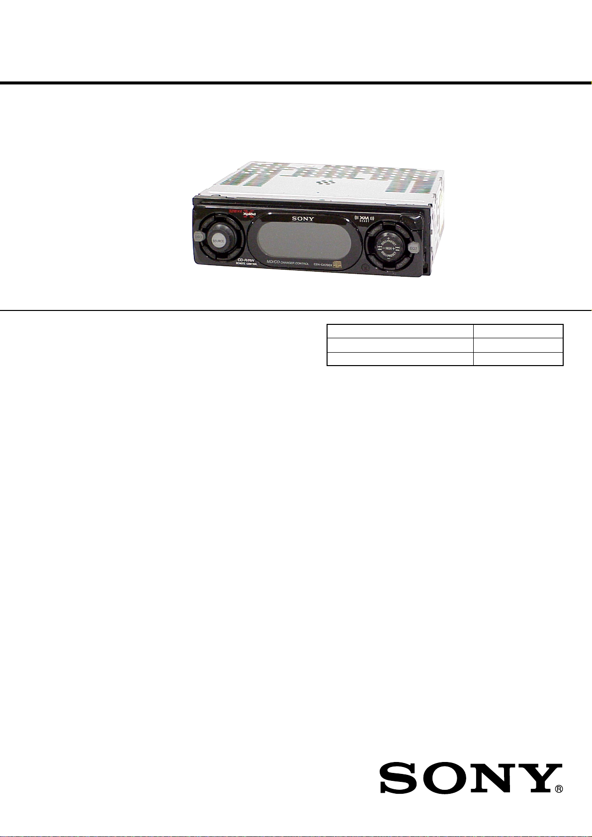
CDX-CA710X/CA790X
SERVICE MANUAL
Ver 1.0 2002. 11
• The tuner and CD sections have no adjustments.
AUDIO POWER SPECIFICATIONS (US Model)
POWER OUTPUT AND TOTAL HARMONIC DISTORTION
23.2 watts per channel minimum continuous average power into
4 ohms, 4 channels driven from 20 Hz to 20 kHz with no more
than 5% total harmonic distortion.
SPECIFICATIONS
CD player section
Signal-to-noise ratio 90 dB
Frequency response 10 – 20,000 Hz
Wow and flutter Below measurable limit
Tuner section
FM
Tuning range 87.5 – 107.9 MHz
Antenna terminal External antenna connector
Intermediate frequency 10.7 MHz/450 kHz
Usable sensitivity 9 dBf
Selectivity 75 dB at 400 kHz
Signal-to-noise ratio 67 dB (stereo),
69 dB (mono)
Harmonic distortion at 1 kHz
0.5% (stereo),
0.3% (mono)
Separation 35 dB at 1 kHz
Frequency response 30 – 15,000 Hz
AM
Tuning range 530 – 1,710 kHz
Antenna terminal External antenna connector
Intermediate frequency 10.7 MHz/450 kHz
Sensitivity 30 µV
US Model
Canadian Model
CDX-CA710X
E Model
CDX-CA790X
Model Name Using Similar Mechanism CDX-CA720X/CA730X
CD Drive Mechanism Type MG-393XA-121//Q
Optical Pick-up Name KSS-720A
Power amplifier section
Outputs Speaker outputs
(sure seal connectors)
Speaker impedance 4 – 8 ohms
Maximum power output 52 W × 4 (at 4 ohms)
General
Outputs Audio outputs (rear)
Power antenna relay control terminal
Power amplifier control terminal
Inputs Telephone ATT control terminal
BUS control input terminal
BUS audio input terminal
Remote controller input terminal
Antenna input terminal
Tone controls Bass ±10 dB at 62 Hz
Treble ±10 dB at 16 kHz
Loudness +8 dB at 100 Hz
+2 dB at 10 kHz
– Continued on next page –
9-874-227-01
2002K0400-1
© 2002. 11
FM/AM COMPACT DISC PLAYER
Sony Corporation
e Vehicle Company
Published by Sony Engineering Corporation
1
Page 2
CDX-CA710X/CA790X
k
Power requirements 12 V DC car battery
(negative ground)
Dimensions Approx. 178 × 50 × 177 mm
(7 1/8 × 2 × 7 in.) (w/h/d)
Mounting dimensions Approx. 182 × 53 × 161 mm
(7 1/4 × 2 1/8 × 6 3/8 in.) (w/h/d)
Mass Approx. 1.2 kg
(2 lb. 10 oz.)
Supplied accessories Parts for installation and connections (1 set)
Front panel case (1)
Card remote commander RM-X118
Design and specifications are subject to change without
notice.
SERVICE NOTES
NOTES ON HANDLING THE OPTICAL PICK-UP BLOCK
OR BASE UNIT
The laser diode in the optical pick-up block may suffer electrostatic
breakdown because of the potential difference generated by the
charged electrostatic load, etc. on clothing and the human body.
During repair, pay attention to electrostatic breakdown and also use
the procedure in the printed matter which is included in the repair
parts.
The flexible board is easily damaged and should be handled with
care.
NOTES ON LASER DIODE EMISSION CHECK
The laser beam on this model is concentrated so as to be focused on
the disc reflective surface by the objective lens in the optical pickup block. Therefore, when checking the laser diode emission, observe from more than 30 cm away from the objective lens.
Notes on Chip Component Replacement
• Never reuse a disconnected chip component.
• Notice that the minus side of a tantalum capacitor may be dam-
aged by heat.
E Model
CLASS 1
CAUTION
Use of controls or adjustments or performance of procedures
other than those specified herein may result in hazardous
radiation exposure.
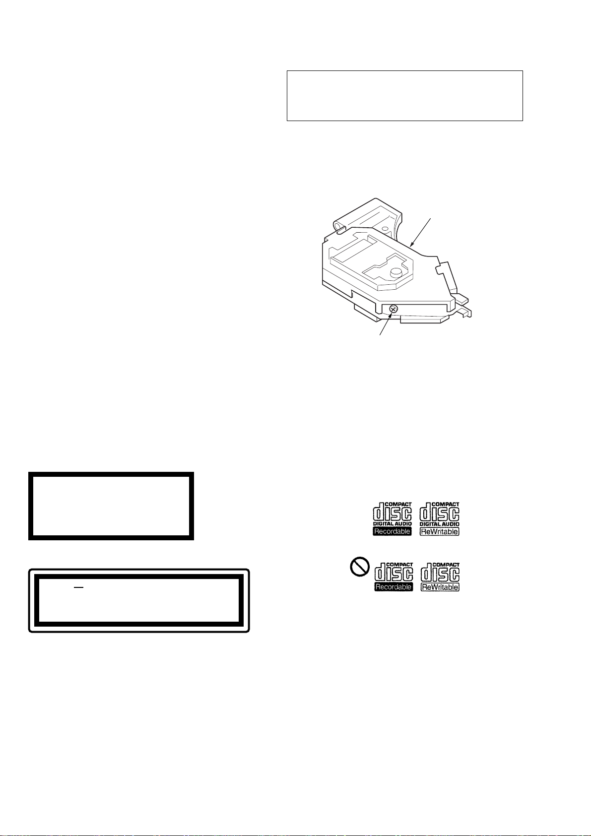
If the optical pick-up block is defective, please replace the whole
optical pick-up block.
Never turn the semi-fixed resistor located at the side of optical
pick-up block.
optical pick-up bloc
semi-fixed resistor
TEST DISCS
This set can playback CD-R and CD-ROM discs. The following
test discs should be used to check the capability:
CD-R test disc TCD-R082LMT (Part No. J-2502-063-1)
CD-RW test disc TCD-W082L (Part No. J-2502-063-2)
Notes on CD-R/CD-RW discs
• You can play CD-Rs (recordable CDs)/CD-RWs (rewritable CDs)
designed for audio use on this unit.
Look for these marks to distinguish CD-Rs/CD-RWs for audio
use.
LASER PRODUCT
This label is located on the bottom of the chassis.
INVISIBLE LASER RADIATION WHEN OPENCAUTION
DO NOT STARE INTO BEAM OR
VIEW DIRECTLY WITH OPTICAL INSTRUMENTS
This label is located on the drive unit’s internal chassis.
When replacing the chassis (T.U) of mechanism deck which have
the “CAUTION LABEL” attached, please be sure to put a new
LABEL (OP CAUTION) (3-223-913-01) to the chassis (T.U).
SAFETY-RELATED COMPONENT WARNING!!
COMPONENTS IDENTIFIED BY MARK 0 OR DOTTED LINE
WITH MARK 0 ON THE SCHEMATIC DIAGRAMS AND IN
THE PARTS LIST ARE CRITICAL TO SAFE OPERATION.
REPLACE THESE COMPONENTS WITH SONY P ARTS WHOSE
PART NUMBERS APPEAR AS SHOWN IN THIS MANUAL OR
IN SUPPLEMENTS PUBLISHED BY SONY.
These marks denote that a disc is not for audio use.
• Some CD-Rs/CD-RWs (depending on the equipment used for
its recording or the condition of the disc) may not play on this
unit.
• You cannot play a CD-R/a CD-RW that is not finalized∗.
∗ A process necessary for a recorded CD-R/CD-RW disc to be
played on the audio CD player.
ATTENTION AU COMPOSANT AYANT RAPPORT
À LA SÉCURITÉ!!
LES COMPOSANTS IDENTIFIÉS P AR UNE MARQUE 0 SUR LES
DIAGRAMMES SCHÉMATIQUES ET LA LISTE DES PIÈCES
SONT CRITIQUES POUR LA SÉCURITÉ DE FONCTIONNEMENT .
NE REMPLACER CES COMPOSANTS QUE PAR DES PIÈCES
SONY DONT LES NUMÉROS SONT DONNÉS DANS CE MANUEL
OU DANS LES SUPPLÉMENTS PUBLIÉS PAR SONY.
2
Page 3
UNLEADED SOLDER
•
Boards requiring use of unleaded solder are printed with the lead
free mark (LF) indicating the solder contains no lead.
(Caution: Some printed circuit boards may not come printed with
the lead free mark due to their particular size.)
: LEAD FREE MARK
Unleaded solder has the following characteristics.
• Unleaded solder melts at a temperature about 40°C higher than
ordinary solder.
Ordinary soldering irons can be used but the iron tip has to be
applied to the solder joint for a slightly longer time.
Soldering irons using a temperature regulator should be set to
about 350°C.
Caution: The printed pattern (copper foil) may peel away if
the heated tip is applied for too long, so be careful!
• Strong viscosity
Unleaded solder is more viscous (sticky, less prone to f low)
than ordinary solder so use caution not to let solder bridges
occur such as on IC pins, etc.
• Usable with ordinary solder
It is best to use only unleaded solder but unleaded solder may
also be added to ordinary solder.
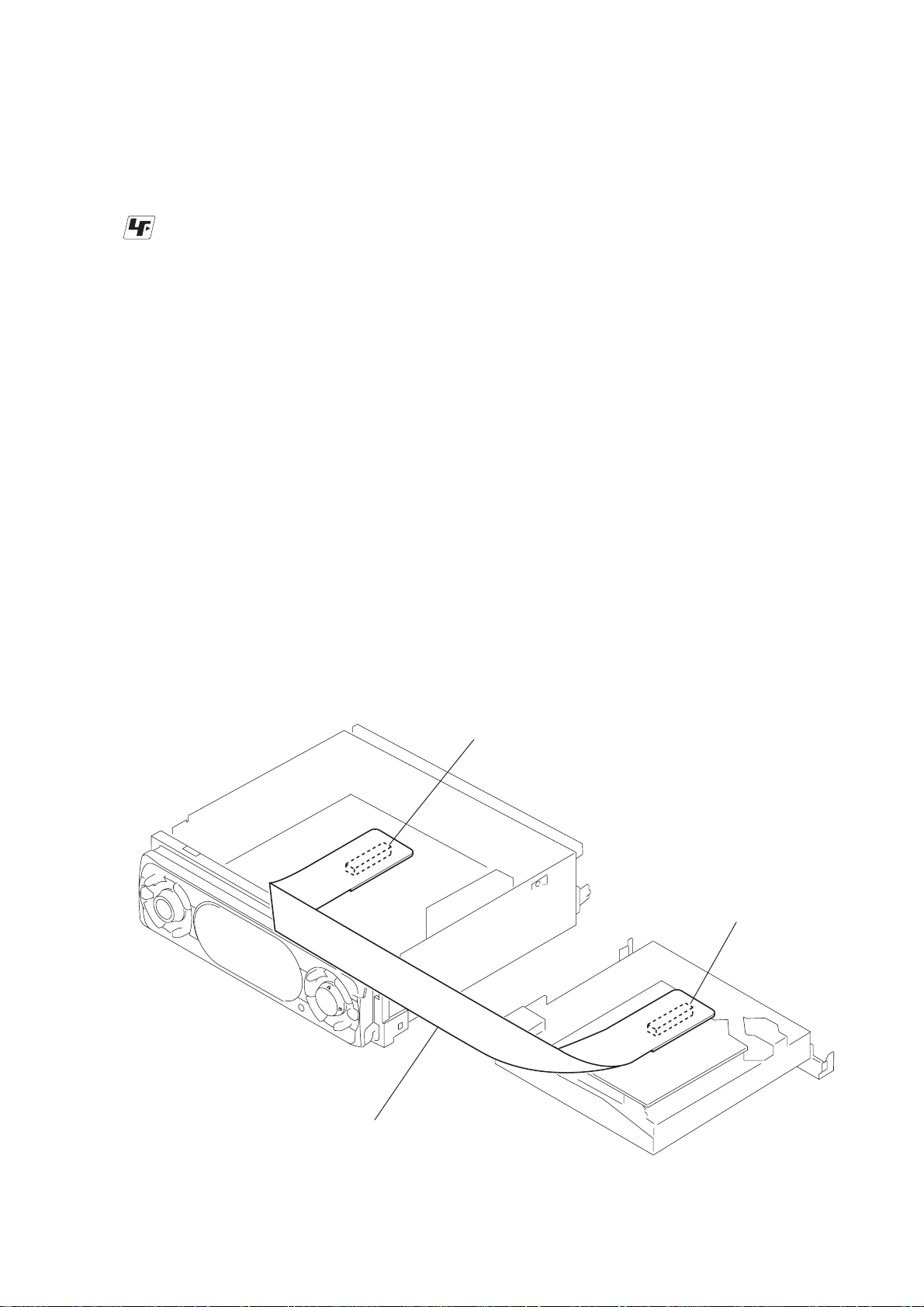
CDX-CA710X/CA790X
EXTENSION CABLE AND SERVICE POSITION
When repairing or servicing this set, connect the jig (extension cable)
as shown below.
• Connect the MAIN board (CNP301) and the SER V O board (CN1)
with the extension cable (Part No. J-2502-011-1).
MAIN BOARD
CNP301
SERVO BOARD
CN1
J-2502-011-1
3
Page 4

CDX-CA710X/CA790X
TABLE OF CONTENTS
1. GENERAL
Location of controls................................................................. 5
Connections ............................................................................. 6
2. DISASSEMBLY
2-1. Sub Panel Assy .................................................................... 7
2-2. CD Mechanism Block ......................................................... 8
2-3. Main Board ......................................................................... 8
2-4. Heat Sink, MJ Board ........................................................... 9
2-5. Chassis (T.U) Assy .............................................................. 9
2-6. Disc In Board .................................................................... 10
2-7. Servo Board....................................................................... 10
2-8. Shaft Roller Assy .............................................................. 11
2-9. Floating Block Assy .......................................................... 11
2-10. Optical Pick-up Block ....................................................... 12
3. DIAGRAMS
3-1. IC Pin Description............................................................. 13
3-2. Block Diagram –CD Section–........................................... 15
3-3. Block Diagram –Tuner Section–....................................... 16
3-4. Block Diagram –Display Section–.................................... 17
3-5. Circuit Boards Location .................................................... 17
3-6. Printed Wiring Boards –CD Mechanism Section–............ 18
3-7. Schematic Diagram –CD Mechanism Section– ................20
3-8. Printed Wiring Boards –Main Section– ............................ 21
3-9. Schematic Diagram –Main Section (1/2)– ........................22
3-10. Schematic Diagram –Main Section (2/2)– ........................23
3-11. Printed Wiring Board –Relay Section– ............................. 24
3-12. Printed Wiring Board –Key Section–................................ 25
3-13. Schematic Diagram –Key Section–................................... 26
3-14. IC Block Diagrams............................................................ 27
4. EXPLODED VIEWS
4-1. Chassis Section ................................................................. 31
4-2. Main Board Section .......................................................... 32
4-3. Front panel Section ........................................................... 33
4-4. CD Mechanism Section (1) ...............................................34
4-5. CD Mechanism Section (2) ...............................................35
4-6. CD Mechanism Section (3) ...............................................36
5. ELECTRICAL PARTS LIST......................................... 37
4
Page 5
SECTION 1
GENERAL
CDX-CA710X/CA790X
This section is extracted
from instruction manual.
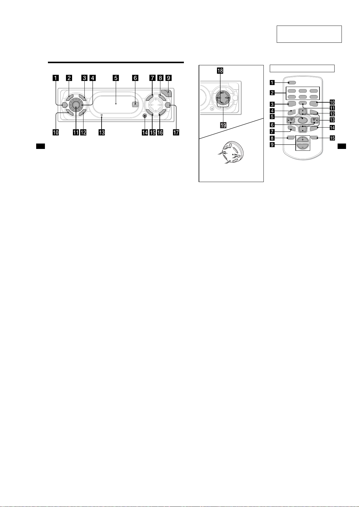
Location of controls
D
E
S
D
P
O
L
M
SOURCE
DSO
O
L
F
R
F
C
S
Refer to the pages listed for details.
a DSO button 20
b MODE button
To c hange the operation.
c DSPL (display mode change) button
10, 12
d Volume control dial
e Display window
f Z (eject) button (located on the front side
of the unit, behind the front panel) 9
g MENU button
To d is play the menus.
h LIST button 12, 15
i OPEN button 8, 9
j OFF (Stop/Power off) button* 8, 9
k SOURCE (Power on/Radio/CD/MD)
button
To s el ec t the source.
4
O
P
E
N
L
U
I
S
N
T
E
M
R
P
E
/
S
C
E
S
I
T
D
SEEK
EQ7
D
I
T
S
E
C
S
/
P
E
R
S
R
O
E
U
T
N
N
D
E
CDX-CA710X
l SCRL (scroll) button 10
m RESET button (located on the front side of
the unit, behind the front panel) 7
n Recepto r for the card remote
commander
o SOUND button 17
p ENTER button
To ente r a setting.
q EQ
*
Warning when installing in a car without
an ACC (accessory) position on the
ignition switch
After turning off the ignition, be sure to press
and hold
disappears.
Otherwise, the display does not turn off and
this causes b
19
7 button
(OFF)
on the unit until the display
attery drain.
O
P
E
N
L
U
I
S
N
T
E
M
R
P
E
/
S
C
E
S
I
T
D
SEEK
EQ7
D
I
T
S
E
C
S
/
P
E
R
S
R
O
E
U
T
N
N
D
E
(DISC/PRESET)
(+): to select upwards
(SEEK)
(–): to select
leftwards/
.
In menu mode, the currently selectable button (s)
of these four are indicated with a “
r DISC/PRESET buttons (+/–)
To receive preset stations, cha ng e th e disc*
skip albums*
*1
When an optional CD/MD unit is connected.
*2
Available only when optional CD unit wit
MP3 file control function is connected.
s SEEK buttons (–/+)
To skip tracks, fast-forward, reverse a trac k,
tune in stations automatically, find a station
manually, and select a setting.
D
(DISC/PRESET)
(–): to select downwards
2
, and select a menu.
(SEEK)
(+): to select
P
/
R
C
E
S
S
I
D
SEEK
I
S
C
/
P
R
E
E
T
T
E
S
rightwards/
>
M
” in the display.
Card remote commander RM-X118
DSPL
REP SHUF
1
4
U
N
E
M
–
SEEK
SOUND
The corresponding buttons of the card
remote commander control the same
functions as those on this unit.
a DSPL button
b Number buttons
(1) REP
(2) SHUF
1
,
To store stations, receive stored stations.
c DSO button
d MENU button
h the
e SOURCE button
f SEEK (</,) buttons
g SOUND button
h OFF button
i VOL (+/–) buttons
j EQ7 button
k MODE button
l LIST button
m DISC (M/m) buttons
n ENTER button
o AT T button
Note
If the display disappears by pressing
be operated with the card remote commander unless
(SOURCE)
on the unit is pressed, or a di s c i s in se rted
to ac
tivate the unit first.
Tip
See “Replacing the lithium battery” on page 21 for
details on how to replace the batteries.
253
MODE
DISC
SOURCE
DISC
VOL
6
EQ7DSO
LIST
+
+
SEEK
–
ENTER
AT TOFF
(OFF)
, it cannot
5
5
Page 6
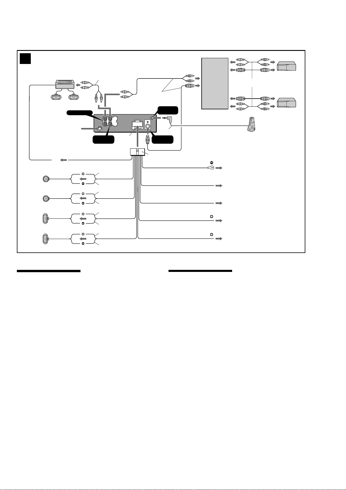
CDX-CA710X/CA790X
Connections
3
from car antenna
à partir de l’antenne de la voiture
3
Left
Gauche
Right
Droit
Left
Gauche
Right
Droit
BUS AUDIO IN
AMP REM
Max. supply current 0.3 A
Courant max. fourni 0,3 A
1
*
BUS
AUDIO
IN
AUDIO OUT
REAR
Blue/white striped
Rayé bleu/blanc
White
Blanc
White/black striped
Rayé blanc/noir
Gray
Gris
Gray/black striped
Rayé gris/noir
Green
Vert
Green/black striped
Rayé vert/noir
Purple
Mauve
Purple/black striped
Rayé mauve/noir
AUDIO
OUT
REAR FRONT
L
R
AUDIO
OUT
Fuse (10 A)
Fusible (10 A)
Supplied with XA-C30
Fourni avec le XA-C30
REMOTE
BUS
CONTROL IN
4
Black
Noir
Blue
Bleu
Light blue
Bleu ciel
Red
Rouge
Yellow
Jaune
IN
2
*
Source selector
(not supplied)
Sélecteur de source
(non fourni)
Max. supply current 0.1 A
Courant max. fourni 0,1 A
ANT REM
ATT
XA-C30
Supplied with the CD/MD changer
Fourni avec le changeur de CD/MD
1
RCA pin cord (not supplied)
*
Cordon à broche RCA (non fourni)
2
Insert with the cord downwards.
*
Insérez avec le câble vers le bas.
1
2
4
5
6
Connection diagram (3)
1
To a metal surface of the car
First connect the black ground lead, then connect
the yellow and red power input leads.
2
To the power antenna control lead or power
supply lead of antenna booster amplifier
Notes
• It is not necessary to connect this lead if there is no
power antenna or antenna booster, or with a
manually-operated telescopic antenna.
•When your car has a built-in FM/AM antenna in
the rear/side glass, see “Notes on the control and
power supply leads.”
3
To AMP REMOTE IN of an optional power
amplifier
This connection is only for amplifiers. Connecting
any other system may damage the unit.
4
To the interface cable of a car telephone
5
To the +12 V power terminal which is energized
in the accessory position of the ignition key
switch
Notes
• If there is no accessory position, connect to the +12
V power (battery) terminal which is energized at
all times.
Be sure to connect the black ground lead to a
metal surface of the car first.
•When your car has a built-in FM/AM antenna in
the rear/side glass, see “Notes on the control and
power supply leads.”
6
To the +12 V power terminal which is energized
at all times
Be sure to connect the black ground lead to a metal
surface of the car first.
Notes on the control and power supply leads
• The power antenna control lead (blue) supplies +12 V
DC when you turn on the tuner.
•When your car has built-in FM/AM antenna in the rear/
side glass, connect the power antenna control lead
(blue) or the accessory power input lead (red) to the
power terminal of the existing antenna booster. For
details, consult your dealer.
•A power antenna without relay box cannot be used
with this unit.
Memory hold connection
When the yellow power input lead is connected, power
will always be supplied to the memory circuit even when
the ignition key is turned off.
Notes on speaker connection
•Before connecting the speakers, tur n the unit off.
• Use speakers with an impedance of 4 to 8 ohms, and
with adequate power handling capacities to avoid its
damage.
• Do not connect the speaker terminals to the car
chassis, or connect the terminals of the right speakers
with those of the left speaker.
• Do not connect the ground lead of this unit to the
negative (–) terminal of the speaker.
• Do not attempt to connect the speakers in parallel.
• Connect only passive speakers. Connecting active
speakers (with built-in amplifiers) to the speaker
terminals may damage the unit.
•To avoid a malfunction, do not use the built-in speaker
wires installed in your car if the unit shares a common
negative (–) lead for the right and left speakers.
• Do not connect the unit’s speaker cords to each other.
Note on connection
If speaker and amplifier are not connected correctly,
"FAILURE" appears in the display. In this case, make sure
the speaker and amplifier are connected correctly.
Schéma de raccordement (3)
1
À un point métallique de la voiture
Branchez d‘abord le fil de masse noir et, ensuite, les
fils d‘entrée d‘alimentation jaune et rouge.
2
Vers le fil de commande de l‘antenne électrique
ou le fil d‘alimentation de l‘amplificateur
d‘antenne
Remarques
• Il n'est pas nécessaire de raccorder ce fil s'il n'y a
pas d'antenne électrique ni d'amplificateur
d'antenne, ou avec une antenne télescopique
manuelle.
• Si votre voiture est équipée d'une antenne FM/AM
intégrée dans la vitre arrière/latérale, voir
“Remarques sur les fils de commande et
d'alimentation”.
3
Au niveau du AMP REMOTE IN de l’amplificateur
de puissance en option
Ce raccordement s’applique uniquement aux
amplificateurs. Le branchement de tout autre
système risque d’endommager l’appareil.
4
Vers le cordon de liaison d’un téléphone de
voiture
5
À la borne +12 V qui est alimentée quand la clé
de contact est sur la position accessoires
Remarques
• S'il n'y a pas de position accessoires, raccordez la
borne d'alimentation (batterie) +12 V qui est
alimentée en permanence.
Raccordez d‘abord le fil de masse noir à un point
métallique de la voiture.
• Si votre voiture est équipée d'une antenne FM/AM
intégrée dans la vitre arrière/latérale, voir
“Remarques sur les fils de commande et
d'alimentation”.
6
À
la borne +12 V qui est alimentée en
permanence
Raccordez d‘abord le fil de masse noir à un point
métallique de la voiture.
Remarques sur les fils de commande et
d'alimentation
• Le fil de commande de l’antenne électr ique (bleu)
fournit une alimentation de + 12 V CC lorsque vous
mettez la radio sous tension.
• Lorsque votre voiture est équipée d’une antenne FM/
AM intégrée dans la vitre arrière/latérale, raccordez la
sortie de commande de l’antenne (bleu) ou l’entrée
d’alimentation des accessoires (rouge) à la borne de
l’amplificateur d’antenne existant. Pour plus de détails,
consultez votre détaillant.
•Une antenne électrique sans boitier de relais ne peut
pas être utilisée avec cet appareil.
Raccordement pour la conservation de la mémoire
Lorsque le fil d’entrée d’alimentation jaune est raccordé,
le circuit de la mémoire est alimenté en permanence
même si la clé de contact est sur la position d’arrêt.
Remarques sur le raccordement des haut-parleurs
•Avant de raccorder les haut-parleurs, mettez l’appareil
hors tension.
•Utilisez des haut-par leurs ayant une impédance de 4 à
8ohms avec une capacité électrique adéquate pour
éviter de les endommager.
•Ne raccordez pas les bornes du système de hautparleur au châssis de la voiture et ne raccordez pas les
bornes du haut-parleur droit à celles du haut-parleur
gauche.
•Ne raccordez pas le câble de masse de cet appareil à la
borne négative (–) de l’enceinte.
•N’essayez pas de raccorder les haut-parleurs en
parallèle.
•Raccordez uniquement des haut-parleurs passifs. Le
raccordement de haut-parleurs actifs (avec
amplificateurs intégrés) aux bornes des haut-parleurs
peut endommager l’appareil.
•Pour éviter tout dysfonctionnement, n’utilisez pas les
fils des haut-parleurs intégrés installés dans votre
voiture si l’appareil partage un fil négatif commun (–)
pour les haut-parleurs droit et gauche.
•Ne raccordez pas entre eux les cordons des hautparleurs de l’appareil.
Remarque sur le raccordement
Si les enceintes et l’amplificateur ne sont pas raccordés
correctement, le message “FAILURE” s’affiche. Dans ce
cas, assurez-vous que les enceintes et l’amplificateur sont
bien raccordés.
6
Page 7
SECTION 2
DISASSEMBLY
Note : This set can be disassemble according to the following sequence.
SET
2-5. CHASSIS (T.U) ASSY
2-1. SUB PANEL ASSY
(Page 7)
(Page 9)
CDX-CA710X/CA790X
2-2. CD MECHANISM BLOCK
(Page 8)
2-3. MAIN BOARD
(Page 8)
2-4. HEAT SINK, MJ BOARD
(Page 9)
2-6. DISC IN BOARD
(Page 10)
2-8. SHAFT ROLLER ASSY
(Page 11)
2-9. FLOATING BLOCK ASSY
(Page 11)
2-10. OPTICAL PICK-UP BLOCK
(Page 12)
Note : Follow the disassembly procedure in the numerical order given.
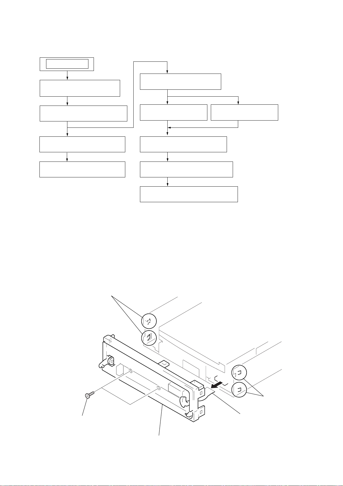
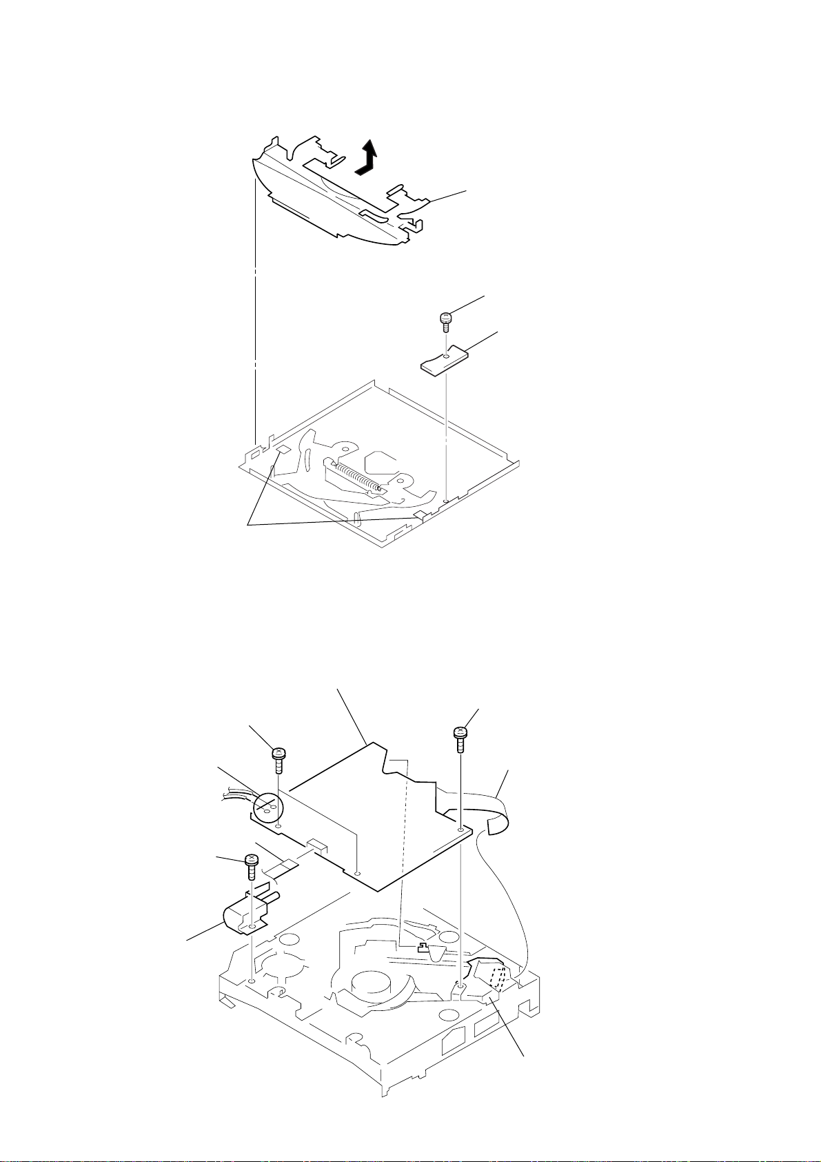
2-1. SUB PANEL ASSY
2-7. SERVO BOARD
(Page 10)
1
PTT 2.6x6
2
claws
5
sub panel assy
4
CN351
3
claws
7
Page 8
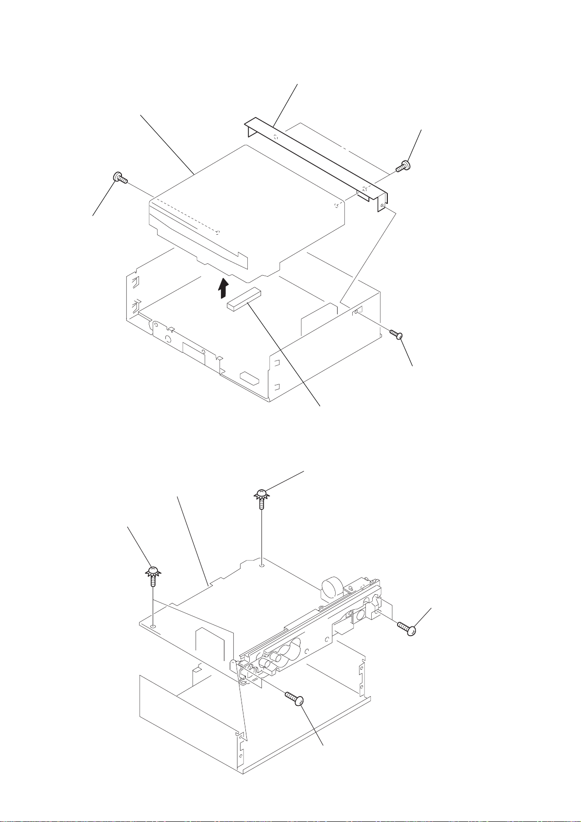
CDX-CA710X/CA790X
4
6
2-2. CD MECHANISM BLOCK
5
CD mechanism block
2
PTT 2.6x6
3
7
bracket (CD)
6
PTT 2.6x
2-3. MAIN BOARD
4
PTT 2.6x6
5
MAIN board
4
3
PTT 2.6x6
CNP301
1
PTT 2.6x6
1
PTT 2.6x
2
PTT 2.6x6
8
Page 9
2-4. HEAT SINK, MJ BOARD
8
5
6
8
MJ board
CDX-CA710X/CA790X
7
4
heat sink
3
PTT 2.6x
2-5. CHASSIS (T.U) ASSY
1
Unsolder the
lead wires.
2
P 2x3
1
PTT 2.6x8
2
PTT 2.6x10
3
P 2x3
4
chassis (T.U) assy
black
red
white
9
Page 10
CDX-CA710X/CA790X
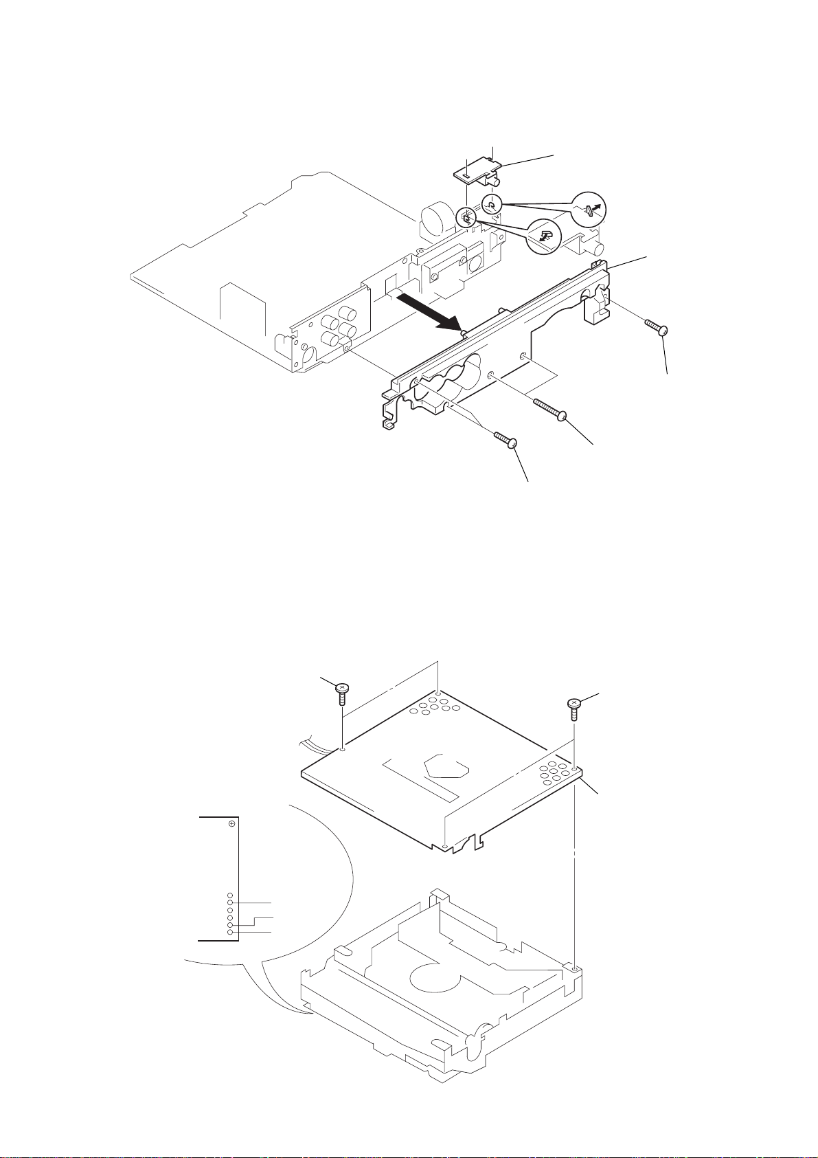
2-6. DISC IN BOARD
4
guide (disc)
1
PS 2x3
2
DISC IN board
2-7. SERVO BOARD
2
Removal the solders.
3
3
P 2x3
claws
5
PS 2x4
1
CN3
7
SERVO board
6
PS 2x4
8
connector
10
4
loading motor assy
optical pick-up block
Page 11
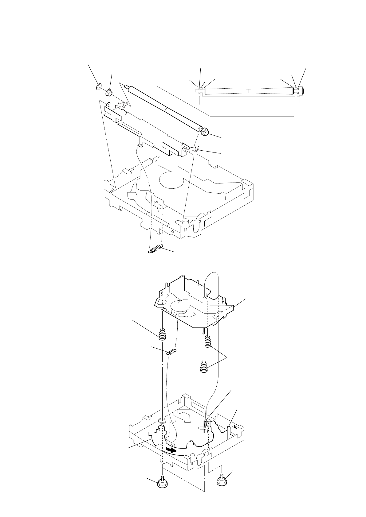
2-8. SHAFT ROLLER ASSY
• When installing, take note of the positions
arm (roller) and washers. (Fig. 1)
3
retaing ring (roller)
4
bearing (roller)
bearing (roller)
retaing ring (roller)
washer (RA)
arm
5
shaft roller assy
2
arm (roller T)
washer (RA)
Fig. 1
CDX-CA710X/CA790X
bearing (roller)
arm
2-9. FLOATING BLOCK ASSY
8
compression spring (FL)
1
tension spring (KF1)
1
tension spring (RA3)
7
floating block assy
9
compression spring (FL)
2
tension spring (KR1)
5
Fit lever (D) in the
direction of the arrow.
6
Turn loading ring in the
direction of the arrow.
4
damper (T)
3
damper (T)
11
Page 12
CDX-CA710X/CA790X
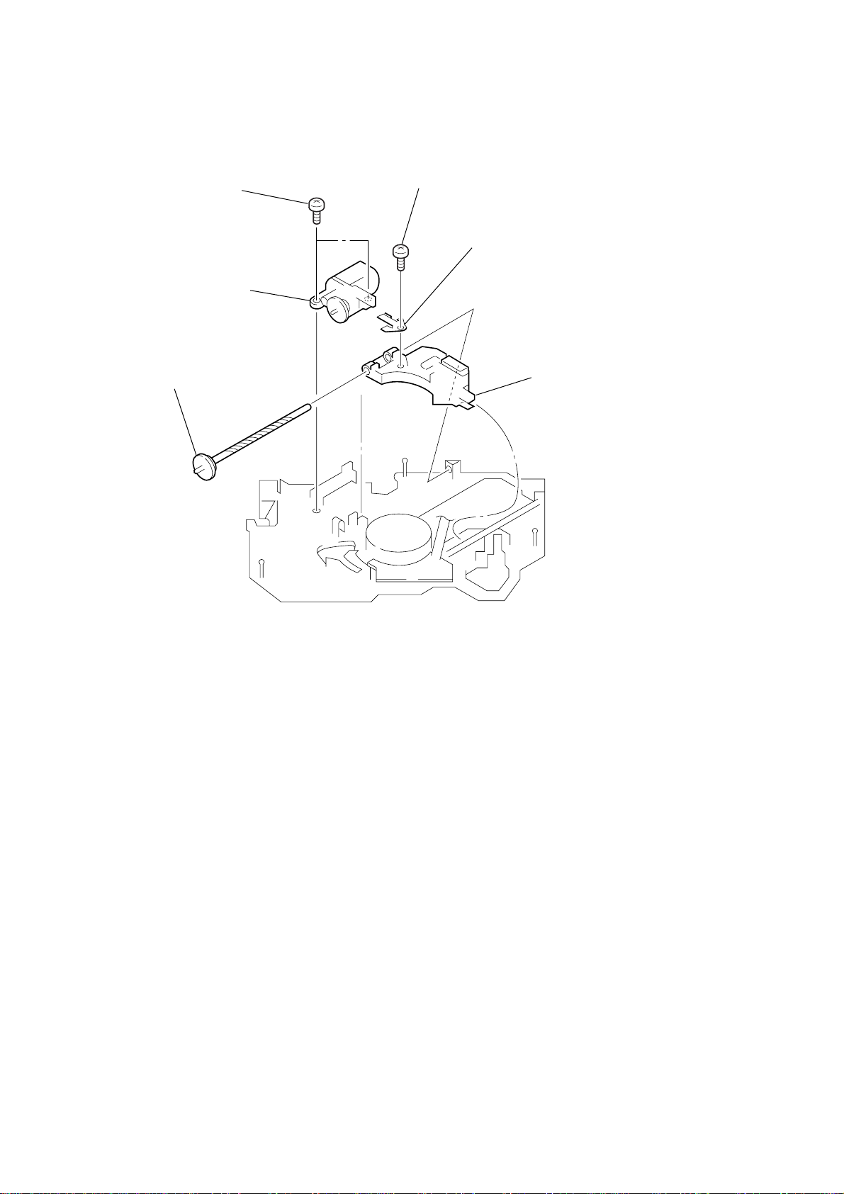
2-10. OPTICAL PICK-UP BLOCK
1
P 2x3
2
sled motor assy
6
shaft (feed) assy
4
P 2x3
5
leaf spring (feed)
3
optical pick-up block
12
Page 13
SECTION 3
DIAGRAMS
3-1. IC PIN DESCRIPTION
• IC303 MN101C49KSD (SYSTEM CONTROL)
Pin No. Pin Name I/O Pin Description
1 VREF– — A/D converter power supply (–) pin
2LVDATA I Spectrum analyzer data input from electronic volume IC.
3 VSM I S-meter voltage detection input
4QUALITY I Noise detection input
5, 6 KEYIN1, 0 I Key input 1, 0
7 RCIN0 I Rotary commander key input
8, 9 NIL I Not used. (Fixed at L in this set)
10 VREF+ — A/D converter power supply (+) pin (+5 V)
11 VDD — Power supply pin (+5 V)
12 OSCOUT O Main clock output (18.43 MHz)
13 OSCIN I Main clock input (18.43 MHz)
14 VSS — Ground
15 XIN I Sub clock input (32.768 kHz)
16 XOUT O Sub clock output (32.768 kHz)
17 MMOD I Memory mode select input (Fixed at L in this set)
18 LCDSO O Serial data output for LCD driver IC.
19 LCDCE O Chip enable output for LCD driver IC.
20 LCDCKO O Serial clock output for LCD driver IC.
21 CD_TSO O Serial data output for CD servo IC.
22 CD_TSI I Serial data input from CD servo IC.
23 CD_TCKO O Serial clock output for CD servo IC.
24 SYSRST O System reset output
25 BUSON O BUS ON output
26 KEYACK I Key acknowledge detection input
27 DAVN I Not used. (Open)
28 BUIN I Backup power supply input
29 SIRCS I SIRCS input
30 TUATTIN I Tuner attenuator control input
31 CD_PACK I CD text pack synchronization signal input from CD servo IC.
32 VDD2 — Power supply pin (+5 V)
33 RESET I Microcomputer reset input
34 NOSESW I Front panel attachment detection input
35 BEEP O Beep output
36 DSTSEL2 I Not used. (Open)
37 TESTIN I Test mode detection input
38 ACCIN I Accessory power supply detection input
39 NCO (VCC) O Not used. (Open)
40 TELATT I Telephone attenuator detection input
41 NCO (VCC) I Not used. (Fixed at H in this set)
42 UNISO O SONY-BUS data output
43 UNISI I SONY-BUS data input
44 UNICKO O SONY-BUS clock output
45 I2C_SIO I/O I2C BUS serial data input/output
46 NCO O Not used. (Open)
47 I2C_CKO O I2C BUS serial clock output
48 STB O Standby control output for power amp IC.
49 DIAG I Mode input from power amp IC.
50 SELFSW I CD mechanism deck Self switch detection input
CDX-CA710X/CA790X
13
Page 14

CDX-CA710X/CA790X
Pin No. Pin Name I/O Pin Description
51 TSTB O CD text parameter strobe output for CD servo IC.
52 RFOK I RFOK signal input from CD servo IC.
53 CD_RST O Reset signal output for CD servo IC.
54 A0 O Command/parameter discrimination signal output for CD servo IC.
55 STB O Data strobe signal output for CD servo IC.
56 X_EN O Not used. (Open)
57 LIMIT I CD mechanism deck Limit switch detection input
58 PH1 I CD mechanism deck PH1 detection input (Not used in this set)
59 D_SW I CD mechanism deck Down switch detection input
60 INSW I CD mechanism deck Disc in switch detection input
61 NC (PH3) O CD mechanism deck PH3 detection input (Not used in this set)
62 CD_LM_LO O CD mechanism deck loading motor control output (Loading direction)
63 CD_LM_EJ O CD mechanism deck loading motor control output (Eject direction)
64, 65 NCO O Not used. (Open)
66 AMPATT O Power amplifier attenuator control output
67 AMPON O Power amplifier standby control output
68 TUON O Tuner power supply control output
69 ATT O System attenuator control output
70 VOLATT O Electronic volume attenuator control output
71 LVCLK O Spectrum analyzer data output for electronic volume IC.
72 AUX_ON O Not used. (Open)
73 – 75 NCO O Not used. (Open)
76 DSTSEL0 I Not used. (Open)
77 DSTSEL1 I Not used. (Open)
78 NCO O Not used. (Open)
79 XCD_ON O Not used. (Open)
80 – 83 NCO O Not used. (Open)
84 NS_MASK O Not used. (Open)
85 DOORIND O Sub panel power supply control output
86 EE_SIO I/O EEPROM serial data input/output
87 EE_CKO O EEPROM serial clock output
88 TUATT O Tuner attenuator control output
89 FLASH_W I Flash microcomputer write detection input
90 NCO O Not used. (Open)
91 AD_ON O Key power supply control output
92, 93 NCO O Not used. (Open)
94 DOORSW I Front panel OPEN/CLOSE detection input
95 DAVSS — D/A converter power supply (–) pin
96, 97 RE_IN1, 0 I Rotary encoder input 1, 0
98 RC_IN1 I Rotary commander SHIFT key input
99 RAMBU I Not used. (Fixed at L in this set)
100 DAVDD — D/A converter power supply (+) pin (+5 V)
14
Page 15

3-2. BLOCK DIAGRAM — CD SECTION —
OPTICAL PICK-UP
KSS-720A
RF AMP,DIGITAL SERVO
DIGITAL SIGNAL PROCESSOR
IC1
CDX-CA710X/CA790X
PD
LD
A
C
B
D
E
F
FOCUS
COIL
I-V
CONV.
LD
DRIVE
Q1
A
84
C
85
B
82
D
83
E
87
F
86
PD
97
A+5V
LD
98
FOCUS/TRACKING COIL DRIVE,
SLED/SPINDLE/LOADING MOTOR DRIVE
FCS-
15
FCS+
16
APC
IC2
FOCUS
COIL
DRIVE
TRACKING
ERROR
(Page 16)
TUNER
LOUT
RF
EQ
FORCUS
ERROR
FD
26
EFM
DEMOD
SERVO
CTL
FDTDSD
62 63 64 65
MD
D/A
CONV
DSUB CODE
PROCESS
I/F
OSC
23 24
X1
16.9344MHz
ROUT
PACK
TSTB
TSCK
TSI
SCK
STB
RST
RFOK
XTALEN
16
12
R-CH
52
56
55
54
SI
8
SO
7
6
5
AO
4
3
2
9
SW5
(DOWN)
CDL
SECTION
A
SYSTEM CONTROL
31
CD_PACK
51
TSTB
21
CD_TSO
22
CD TSI
23
CD TCKO
55
STB
54
AO
53
CD_RST
52
RFOK
59
D SW
IC303 (1/3)
TRACKING
COIL
M902
(SLED)
M901
(SPINDLE)
M903
(LOADING)
50
TRK+
17
TRK-
18
SL-
M
13
SL+
14
SP-
M
11
SP+
12
LD-
M
9
LD+
10
TRACKING
COIL
DRIVE
SLED
MOTOR
DRIVE
SPINDLE
MOTOR
DRIVE
LOADING
MOTOR
DRIVE
TD
23
SD
5
MD
6
LOAD
1
EJECT
2
SW2
(SELF)
SW1
(DISC IN)
SW3
(LIMIT)
SELF SW
INSW
60
57
LIMIT
CD_LM _LO
62
63
CD_LM_ EJ
RESET
IC302
33
1
S303
(RESET)
RESET
2
U-COM+5V
• Signal path
:CD
• R-ch is omitted due to
same as L-ch.
15 15
Page 16

CDX-CA710X/CA790X
3-3. BLOCK DIAGRAM — TUNER SECTION —
J501
(ANTENNA)
BATT
CN101
BUS
CONTROL IN
TUNER UNIT
TUX501
ANT
1
MUTE CONDITION
E2PROM SDA
E2PROM SCL
D104
D105
8
3
2
1
7
S-METER
TU MUTE
6
5
4
BATT
L
R
VCC
TU VDD
TU SDA
TU SCL
BATT CHECK
10
11
14
13
17
16
Q101
J401
L
-1
ELECTRONIC VOLUME
IC401
R-CH
BUS AUDIO IN
R
-2
(Page 15)
PDL+
A
CD
AU8V
BUS INTERFACE
BATT
3
BUSON
1
DATA I/O
6
CLK
4
SECTION
IC301
B/U-C
BUSON
DATA IN
DATA OUT
CLK IN
RST
4
R-CH
3
TUNER
+5V REG
Q501
6
8
7
R-CH
CDL
R-CH
R-CH
10
12
9
8
11
13
4
7
42
43
40
41
14
16
15
13
12
45
47
70
2
71
3
30
88
86
87
28
25
42
43
44
24
PDR+
MDL
MDR
AML
AMR
SAIN
SAOUT
MUTE
SCL
SDA
I2C SIO
I2C CKO
VOL ATT
LV DATA
LV CLK
VSM
TU ATT IN
TU ATT
EE SIO
EE CKO
BU IN
BUSON
UNISO
UNISI
UNICKO
SYSRST
OUTLR
OUTRR
ACOUTL
ACINL
ACINR
OUTLF
OUTRF
SYSTEM CONTROL
IC303 (2/3)
TEST IN
TEL ATT
ACC IN
ATT
BEEP
STB
DIAG
24
R-CH
21
32
31
R-CH
33
25
22
R-CH
69
35
48
49
37
40
38
LINE MUTE
CONTROL
Q401,402
MUTE
Q406
MUTE
Q404
A5V
D5V
AU5V
U-COM+5V
DR6V
AU8V
KEY+B
POWER AMP/VOLTAGE REGULATOR
12
11
4
2
16
22
25
31
33
37
30
34
ACC DET
Q102
FL IN
IN FL
RL IN
IN RL
SCL
SDA
ACGND
STB
DIAG
IC201
REG
TEL ATT SW
Q103
SW
FL+
FL-
RL+
RL-
VP1
VP2
SW1
SW2
R-CH
5
3
9
7
20
6
29
27
VP
35
BATT
R-CH
D120
D121
BATT
BATT
-3
-4
CNP101
10
12
11
18
17
16
15
13
1
9
2
4
3
5
6
7
8
L
R
FL+
FL-
RL+
RL-
FR+
FR-
RR+
RR-
AMP R
ANT R
+B
TEST
ATT
ACC
GND
AUDIO OUT
F901
10A
• Signal path
: FM
: AM
RST
2
: CD
• R-ch is omitted due to same as L-ch.
1616
Page 17

3-4. BLOCK DIAGRAM — DISPLAY SECTION — 3-5. CIRCUIT BOARDS LOCATION
)
CDX-CA710X/CA790X
KEY MATRIX
LSW901,902,904,905,907,
911,913,915,916,918,919
S903,912,914,917
CNJ101
(REMOTE IN)
LED802
Z
LED801
(DOOR INDICATOR)
SUB
BOARD
D303
D302
S801
Z
IC971
REMOTE
RECEIVE
S302
(NOSE)
DOOR IND
SWITCH
Q303
32.768kHz
ROTARY
ENCODER
RE901
KEY
ACTIVE
Q304
X301
SYSTEM CONTROL
IC303 (3/3)
KEY IN0
6
KEY IN1
5
KEY ACK
26
AD ON
91
RC IN1
98
RC IN0
7
SIRCS
29
NOSESW
34
DOORIND
85
XIN
15
XOUT
16
REIN0
97
REIN1
96
DOOR SW
94
LCD SO
LCD CKO
LCD CE
OSC OUT
OSC IN
LCD DRIVE
IC901
DISC IN board
MJ board
SUB (CD) board
DATA
100
99
98
LCD DATA
CLK
LCD CLK
CE
LCD CE
SEG1
SEG84
COM1
COM4
3
|
|
86
LCD
LCD901
90
|
|
87
LIMIT board
18
20
19
tuner unit
(TUX501
KEY+B (10V)
LSW901,902,904,905,907,
911,913,915,916,918,919
LED903,912,914,917,931,941
951-954
KEY
()
ILLUMINATION
KEY board
SUB board
MAIN board
SERVO board
• Waveforms
12
13
X302
18.43MHz
— Servo Board —
(MODE: CD PLAY)
1
16.9344MHz
wd
(XTAL)
IC1
2
1.8Vp-p
— Main Board —
1
18.432MHz
IC303
(OSCOUT)
qs
2
1.8Vp-p
5.2Vp-p
IC1
3.3msec
(PACK)
ts
5Vp-p
IC303
32.768kHz
(XOUT)
qh
3
1.5Vp-p
uj
(RFO)
IC1
4
0V
Approx. 100mVp-p
oa
(FEO)
IC1
5
Approx. 100mVp-p
od
(TEO)
IC1
0V
17 17
Page 18

CDX-CA710X/CA790X
3-6. PRINTED WIRING BOARDS — CD MECHANISM SECTION — • Refer to page 17 for Circuit Boards Location.
THIS NOTE IS COMMON FOR PRINTED WIRING
BOARDS AND SCHEMATIC DIAGRAMS.
(In addition to this, the necessary note is
printed in each block.)
for schematic diagram:
• All capacitors are in µF unless otherwise noted. pF: µµF
50 WV or less are not indicated except for electrolytics
and tantalums.
• All resistors are in Ω and 1/
specified.
•%: indicates tolerance.
f
•
• C : panel designation.
• A : B+ Line.
• Power voltage is dc 14.4V and fed with regulated dc power
•Voltages are taken with a V OM (Input impedance 10 MΩ).
•Waveforms are taken with a oscilloscope.
• Circled numbers refer to waveforms.
• Signal path.
: internal component.
Note:
The components identified by mark 0 or dotted
line with mark 0 are criti-
cal for safety.
Replace only with part
number specified.
supply from ACC and BATT cords.
Voltage variations may be noted due to normal produc-
tion tolerances.
Voltage variations may be noted due to normal production tolerances.
F : FM
f : AM
J : CD
4
W or less unless otherwise
Note:
Les composants identifiés par
une marque 0 sont critiques
pour la sécurité.
Ne les remplacer que par une
piéce portant le numéro
spécifié.
: Uses unleaded solder.
CN2
234567891011121314
1
A
B
C
D
E
F
for printed wiring boards:
• X : parts extracted from the component side.
• Y : parts extracted from the conductor side.
• x : parts mounted on the conductor side.
a
•
• : Pattern from the side which enables seeing.
Caution:
Pattern face side: Parts on the pattern face side seen from the
(Side B) pattern face are indicated.
Parts face side: Parts on the parts face side seen from the
(Side A) parts face are indicated.
: Through hole.
(The other layer’s patterns are not indicated.)
G
SW5
H
I
1818
Page 19

: Uses unleaded solder.
CDX-CA710X/CA790X
A
B
C
D
E
F
G
H
1
M903
234567891011121314
TP66
TP73
TP53
TP64
TP75
TP86
TP87
TP47
TP69
TP57
R21
TP68
R20
TP54
TP48
R22
TP76
TP52
TP74
FB5
TP50
TP56
C71
TP51
TP58
TP61
C44
R31
TP62
TP85
TP7
CN1
TP49
TP91
TP90
TP19
CN3
TP80
TP60
TP59
TP71
C26
TP63
R26
TP8
TP72
R19
TP77
TP55
C4
R17
TP9
TP78
TP70
C27
TP20
Q1
C6
R30
R3
C25
X1
R18
C41
TP17
C3
C34
C29
TP92
TP16
C5
R29
TP79
C17
C22
C1
TP11
C9 C10
C8
C16
C36
TP34
TP35
R7
R6
C43
TP12
TP36
C70
C38
C15
TP38
TP39
TP82
IC1
TP46
BP2
IC2
TP81
TP37
TP40
BP1
TP41
TP30
C11
TP83
C14
C18
TP45
TP42
R12
C30
TP28
R5
C13
C24
TP44
TP43
TP31
R10
TP26
TP89
R9
R8
TP23
C35
TP33
TP32
R15
TP27
TP84
TP10
TP88
BP3
R14
TP29
C20
C19
TP15
C23
TP22
TP24
TP25
TP14
BP4
TP18
TP21
TP1
TP5
TP3
TP2
TP4
TP6
(Page 21)
SW1
SW3
SW2
CN1
I
19 19
M902
M901
Page 20

CDX-CA710X/CA790X
3-7. SCHEMATIC DIAGRAM — CD MECHANISM SECTION — • Refer to page 27 for IC Block Diagrams.
SW3
CN2
TP77
TP78
C1
TP81
TP82
TP83
TP84
R29
R30
C5
TP79
TP80
C43
• Refer to page 17 for Waveforms and page 18 for Common Note on Schematic Diagram.
Q1
TP9 TP8
R26
R3
C4
C3
TP7
C6
C14
TP10
C13
C11
R5
C15
C10
C9
TP12
TP11
TP89
C18
C19
C20 C23
R9
C24
TP24
TP25
TP22
TP23
R8
TP88
IC1
C35
TP36
TP45
TP44
TP43
TP42
TP41
TP40
TP39
TP38
TP37
TP46
C38
M902
M901
SW1
SW2
CN1
TP4
TP2
TP3
CN3
M903
SW5
TP93
TP94
TP95
TP96
TP97
TP98
TP1
TP5
TP85
TP92
TP87
TP86
C8
TP35
TP34
C16C70
IC B/D
C17
C41
C27
C26
R12
C30
R10
TP31
TP30
R15
TP90
TP91
TP27
TP29
TP26
TP28
R7
TP15
TP21
BP3
TP14
BP4
R6
TP18
TP17
TP20
TP16
TP19
C22
IC2
BP1
C29
R14
C25
C34
X1
C71
TP33
BP2
TP32
C36
C44
R31
FB5
R22
R21
R18
R19
R20
R17
TP66
TP61
TP76
TP60
TP75
TP59
TP74
TP58
TP73
TP57
TP72
TP56
TP71
TP55
TP70
TP54
TP69
TP53
TP68
TP52
TP51
TP50
TP64
TP49
TP48
TP63
TP47
TP62
CN1
(Page 23)
IC B/D
Note:
•Voltage is dc with respect to
ground under no-signal conditions.
no mark : CD PLAY
2020
Page 21

CDX-CA710X/CA790X
3-8. PRINTED WIRING BOARDS — MAIN SECTION — • Refer to page 17 for Circuit Boards Location and page 18 for Common Note on Printed Wiring Boards.
A
B
C
D
E
F
G
H
1
R502
C504
C508
FB503
I
JW126
JW127
2345678910111213
J401
J501
CN101
C206
TUX501
R522
R523
C505
R504
R517
C510
D307
R503
Q501
R505
C409
JW87
JW92
JW125
D309
JW88
C502
C326
JW79
R501
C501
D501
D305
C322
R409
C327
C408
JW55
JW56
R411
C434
C520
CN351
C407
JW83
JW84
JW85
JW86
R358
D308
C325
R413
JW78
R423
R412
C420
C419
C433
JW91
JW123
JW124
R406
R410
JW80
JW81
R424
JW90
D304
C406
Q406
R408
C418
JW89
C405
JW54
JW101
D306
R405
Q405
JW82
C416
D503
R357
R356
R352
R354
JW100
JW122
R360
R404
Q404
JW53
L401
JW77
IC401
JW99
JW67
C423
R421
JW98
JW110
JW121
JW50
R403
Q403
JW71
JW72
JW73
JW74
JW76
C421
JW97
JW120
R350
R351
R359
R353
R355
C212
JW69
JW75
Q303
R365
C214
JW68
R414
R415
C432
R362
R363
R364
JW119
JW70
C422
R426
JW96
JW118
C424
C430
R418
R420
R419
JW57
C413
C425
JW95
R322
R361
JW117
JW51
C415
R323
JW116
JW66
C414
C412
JW107
C227
C226
R401
D401
D403
Q402
R416
C426
R417
C427
C428
C429
JW115
C215
JW52
C223
JW65
C402
Q401
JW94
R345
JW114
JW64
R316
R315
R314
R311
R309
R344
JW2
JW63
C401
JW113
C221
JW62
C308
C309
JW61
FB303
JW93
R310
R308
IC303
JW112
R343
IC201
JW60
L303
C306
R303
R313
R312
JW111
D302
D303
JW59
R307
R306
C207
R204
JW58
C317
R333
C203
R201
R203
CNP301
C313
IC302
R324
X302
Q304
C205
C201
C304
C331
R206
C219
C204
JW49
JW1
JW18
C332
C303
C305
JW39
R325
JW48
C315
R334
R332
JW14
JW17
FB301
FB302
R305
C316
JW4
JW5
JW6
JW7
JW8
R205
C218
R202
C202
JW13
C307
FB304
X301
S303
C302
C301
FB305
JW38
C312
C314
R304
JW37
R330
R331
JW11
D110
L301
R329
L302
JW9
JW10
D111
JW16
JW36
JW19
JW20
D112
JW35
CNP101
D113
JW34
R112
D114
JW21
JW33
JW41
JW42
JW43
JW44
JW45
JW46
JW47
F901
D115
D121
JW32
C104
C105
D116
D120
JW31
C310
D117
R109
Q103
IC301
JW3
JW12
C318
R103
R111
R110
Q102
JW23
R105
R320
JW40
S302
C103
C333
R327
R108
R107
R102
R101
D105
D104
JW24
C102
R346
JW30
D106
R106
R104
JW25
R335
D119
D118
R328
Q101
C334
D109
JW22
C101
CN102
C107
C106
L101
TH100
JW15
D102
D103
D101
D122
JW26
JW27
JW28
JW29
C311
: Uses unleaded solder.
CNJ101
(Page 19)
CN103
• Semiconductor
Location
Ref. No. Location
D101 E-10
D102 E-10
D103 E-10
D104 F-9
D105 E-9
D106 D-9
D109 C-10
D110 D-7
D111 D-8
D112 D-8
D113 D-8
D114 D-8
D115 D-8
D116 D-8
D117 D-9
D118 D-9
D119 D-9
D120 E-8
D121 E-8
D122 F-10
D302 I-6
D303 I-6
D304 I-3
D305 I-2
D306 J-3
D307 I-2
D308 I-3
D309 I-2
D401 E-5
D403 E-5
D501 F-2
IC201 B-6
IC301 H-9
IC302 H-6
IC303 H-5
IC401 F-4
Q101 F-10
Q102 E-9
Q103 E-9
Q303 G-4
Q304 I-6
Q401 F-5
Q402 E-5
Q403 C-4
Q404 C-4
Q405 C-3
Q406 C-3
Q501 F-2
J
(Page 24)
21 21
Page 22

CDX-CA710X/CA790X
• Refer to page 18 for Common Note on Schematic Diagram.
3-9. SCHEMATIC DIAGRAM — MAIN SECTION (1/2) — • Refer to page 29 for IC Block Diagrams.
C201
R201
C202
CNP101
C203
R202
IC B/D
IC201
C204
C205
C206 C207
R203 R204
R205 R206
C218 C219
C221
C212
C223
C227
C214
C226
C215
L401
R401
D403
C416
D401
C402
C401
Q402
Q403
Q404
Q405
Q406
Q401
C418
C420
R403
R404
R405
R406
C409
R408
R410
R423
C407
C408
C405
C406
R413
J401
R409
R412
R411
J501
TUX501
F901
L101
C103
R103
D109
D106
D111
D110
D113
D112
D114
D115
D116
C105
D119
D117
R108 R107
D118
C104
C102
R111
R112
D120
D121
R110
R105R106
R109
R104
Q103
Q102
C413
C412
C423
C424
C414
C415
C426
C427
C422
R426
R414
C421
R415
C425
R416
R417
IC B/D
C428
R418
R419
C429
R420
C430
R421
C432
IC401
C419
C433
C434
JW120
C508
R505
R522
R523
R504
C510
R502
FB503
R503
C501
C504
R517
R501
C505
Q501
D501
C502
(Page 23)
2222
Note:
•Voltage is dc with respect to ground under
no-signal (detuned) condition.
no mark : FM
(): AM
<>: CD PLAY
Page 23

• Refer to page 17 for Waveforms and page 18 for Common Note on Schematic Diagram.
3-10. SCHEMATIC DIAGRAM — MAIN SECTION (2/2) — • Refer to page 28 for IC Block Diagrams.
(Page 22)
(Page
L301
L303
FB305
C305
FB304
C301
C303
FB302
C304
FB301
C331
R304
R305
C332C302
20)
CNP301
R303
C306
C309
CDX-CA710X/CA790X
C307
C308
FB303
Q101
C101
D101
D104
D105
R320
C310
D103
D102
C333 C318
CN103
R101
R102
TH100
CN101
D122
R335
CNJ101
Note:
•Voltage is dc with respect to ground
under no-signal (detuned) condition.
no mark : FM
(): AM
<>: CD PLAY
IC B/D
IC301
S302
S303
CN102
R328
C106
C107
C313
C311
C334
L302
C312
IC302
R322
R323
R324
R325
R327
R346
C520
R306
R307
R308
R329
R309
R316
R315
R314
R313
R312
R311
R310
IC303
C317
X301
C316
C315
C314
R331
R330
23 23
X302
R333 R334
R332
D302
D303
R424
R350
R351
R353
R354
R355
R352
Q304
R356R357
R343 R344
R345
D503
R359
R358
R361
Q303
R360
R365
D304
R364R363R362
C325
C327
C322
C326
D305
D307
D306
D309
D308
CN351
(Page 26)
Page 24

CDX-CA710X/CA790X
3-11. PRINTED WIRING BOARD — RELAY SECTION — • Refer to page 17 for Circuit Boards Location and page 18 for Common Note on Printed Wiring Boards.
1
2345678910
(Page 21)
A
B
CN801
C
D
: Uses unleaded solder.
E
F
G
H
LED802
CN802
LED801
S801
I
(Page 25)
2424
Page 25

CDX-CA710X/CA790X
Administrator SV-CDXCA710X-KEY-S
3-12. PRINTED WIRING BOARD — KEY SECTION — • Refer to page 17 for Circuit Boards Location and page 18 for Common Note on Printed Wiring Boards.
1
234567891011121314
A
LSW904
B
C
LED951
LED952
LED903
S903
LSW902
LSW901
LSW905
LED953
LSW907
LED931
LED941
D
: Uses unleaded solder.
LSW919
LSW916
LED954
LSW918
LSW913
LSW911
IC971
LED917
S917
LED914
S914
LSW915
LED912
S912
E
F
G
H
RE901
R921
R902
R948
R904
R987
R905
R947
R907
R903
R906
R901
R920
R922
R983
R942
R946
R971
R970
R941
R940
R986
R985
R984
R990
D901
D908
R993
C961
C952
C956
C953
R991
R999
R992
R994
C962
IC901
R995
R996
D913
R938
R937
R936
D912
C971
R976
D911
D972
D903
R997
D971
R998
R911
CN901
R928
R959
R927
R926
R912
R950
R951
R958
R913
R982
R919
R914
R932
R931
R915
R916
R918
R917
• Semiconductor Location
I
Ref. No. Location
D901 G-6
D903 F-11
D908 F-6
D911 H-10
D912 H-10
D913 G-9
D971 F-11
D972 F-10
Ref. No. Location
LED903 B-1
LED912 C-13
LED914 B-14
LED917 B-13
LED931 B-4
LED941 C-11
LED951 B-3
LED952 B-2
(Page 24)
LED953 C-4
IC901 G-7
LED954 B-11
IC971 D-11
25 25
Page 26

CDX-CA710X/CA790X
3-13. SCHEMATIC DIAGRAM — KEY SECTION — • Refer to page 18 for Common Note on Schematic Diagram.
(Page 23)
CN801
S801
R920
R921
R922
LSW902(2/2)
LSW904(2/2)
LSW905(2/2)
LED801
LED802
LED953 LED954
R946
LED951
R947
R948
LED952
CN802
R931
R932
LSW919(2/2)
LED917
LED912
CN901
RE901
R959R958
R926
R927
R928
R940
R941
R942
LSW911(2/2)
LSW901(2/2)
LSW907(2/2)
D903
R950
R951
LSW913(2/2)
LSW915(2/2)
LSW916(2/2)
LSW918(2/2)
R976
R970
R971
LSW911(1/2)
S912
LSW913(1/2)
S914
LSW915(1/2)
LSW916(1/2)
S917
LSW918(1/2)
LSW919(1/2)
LED941
LED931
R911
R912
R913
R914
R915
R916
R917
R918
R919
R901
R902
R903
R904
R905
R906
R907
LED914
R982
R983
R987
LED903
LSW901(1/2)
LSW902(1/2)
S903
LSW904(1/2)
LSW905(1/2)
LSW907(1/2)
R984
R990
C956
R985
R986
R995
R996
D901
D972
C971
D908
R999
C952
IC971
R991
C953
R998
R997
C962C961
R937
R936
R938
D971
R992
R993
R994
IC901
LCD901
D913
D912
D911
Note:
•Voltage is dc with respect to ground under no-signal
(detuned) condition.
no mark : FM
2626
Page 27

3-14. IC BLOCK DIAGRAMS
76
75
AGCI
AGCO74RFI73C3T72ASY71EFM70AVDD697E DAC3687D DAC2677C DAC1667F DAC065MD64SD63TD62FD
60
ATEST59TEST158TEST057DGND56TSTB55TSCK54TSI53TSO52PACK51DVDD
61
AGND
1
DGND
2
RFOK
3
RST
4A05
STB
6
SCK
7SO8SI9
XTALEN
10
DVDD
11
DAVDD
12
ROUT
13
DAGND
REGC
16
LOUT
17
DAVDD
18R+19R–20L+21L–22
XVDD
23
XTAL24XTAL
25
XGND
1514
DAGND
77
RFO
78
EQ2
79
EQ1
80
RF-
81
AGND
82
A
83
C
84
B
85
D
86
F
87
E
88
AVDD
89
REFOUT
90
FE-
91
FEO
92
TE-
93
TEO
94
TE2
95
AGND
TEC
96
PD
97
98
LD
PN
99
100
AVDD
50
C2D3
49
C2D2
48
C2D1
47
C1D2
46
C1D1
45
DGND
44
PLCK
43
MIRR/WFCK
42
RFCK
41
LOCK
40
DVDD
39
TSOI
38
C16M
37
DGND
36
TX
35
HOLD/WDCK
34
LRCK
33
LRCKIN
32
SCKO
31
SCKIN
30
DOUT
29
28
DIN
FLAG
27
EMPH
26
DVDD
EFM
COMPARATOR
EFM
EFM
DEFECT
FOK
A3T
MIRR
FEO
TEO
TEOFS
FEOFS
RF
AMP BLOCK
SWITCH
MICROCOMPUTER INTERFACE
SCF
OSC
FOCUS
REGISTER
TRACKING
REGISTER
OCTUPLED
OVERSAMPLING DIGITAL FILTER
NOISE SHAVER
OUTPUT BUFFER
NOISE SHAVER
OUTPUT BUFFER
DE-EMPHASIS CIRCUIT
D/A
INTERFACE
CIRCUIT
OUTPUT PROCESSOR
DIGITAL
AUDIO
INTERFACE
DIGITAL PLL
TIMING GENERATOR
EFM DEMODULATOR
ERROR
CORRECTION
PROCESSOR
MICROCOMPUTER INTERFACE
CD-TEXT DECODER
SUB-CODE PROCESSOR
16K
SRAM
D/A
AUTO GAIN
CONTROLLER
FD/TD/SD/MD
CONTROLLER
ADDER
SVDRAM
MULTIPLIER
SVCRAM
SVROM
ROM
DECODER
CLV
PROCESSOR
DEFECT
COMPARATOR
RFENV
MIRENV
A/D CONVERTER
MEMORY
PROCESSOR
COMPARATOR
IC1 µPD63711GC-8EU (Servo Board)
CDX-CA710X/CA790X
27
Page 28

CDX-CA710X/CA790X
FWD
IC2 BA5810FP-E2 (Servo Board)
1
BIAS
28
REV
LDCONT
IN1
IN2
PREVCC
POWVCC
VOL–
VOL+
VO2–
VO2+
VO1–
VO1+
PS
2
3
4
5
6
7
8
9
10
10k
11
12
10k
10k
13
14
10k
X3
POWER
PREVCC
(PRE.LOADING)
POWVCC12
(CH1.CH2)
–
+
+
–
–
+
+
–
SAVE
10k
10k
10k
10k
LOADING PRE
7.5k
–
16k
LEVEL
SHIFT
FWD REV
7.5k
16k
+
LEVEL
SHIFT
+
–
+
7.5k
–
+
–
+
–
16k
27
26
25
24
23
22
OPIN4+
OPIN4–
OPOUT4
OPIN3+
OPIN3–
OPOUT3
7.5k
LEVEL
SHIFT
+
LEVEL
SHIFT
–
CH1-4
MUTE
16k
POWVCC34
(CH3,CH4)
10k
10k
10k
10k
–
+
+
–
–
+
+
–
10k
10k
10k
10k
21
20
19
18
17
16
15
MUTE
POWVCC
GND
VO3–
VO3+
VO4–
VO4+
28
IC301 BA8270F-E2 (Main Board (2/2))
BUS ON
1
2
RST
BATT
3
4
CLK
5
VREF
6
DATA
I/O
GND
7 8
BUS ON
SWITCH
RESET
SWITCH
BATTERY
SWITCH
14
13
12
11
10
9
VCC
RST
BUS ON
CLK IN
B/U-C
DATA IN
DATA OUT
Page 29

IC201 TDA8588J/N1 (Main Board (1/2))
TAB
1
FL-
3
PROTECTION
DIAGNOSTIC
FL
RL
MUTE
MUTE
RR
FL+
RL-
RL+
IN_RL
SGND
IN_RR
RR+
RR-
5
7
9
11
13
15
17
19
CDX-CA710X/CA790X
2
SDA
I2C BUS
4
SCL
6
VP2
8
PGND3
10
SVR
IN_FL
12
14
IN_FR
16
18
ACGND
PGND2
VP
FR+
FR-
DIAF
SW2
SW1
SERVO
MECHA
U-COM
20
22
24
26
28
30
32
34
36
VP1
STB
PGND1
RST
CRES
AU8V
GND
DISP+B
CBU
21
STANDBY
MUTE
TEMPERATURE
PROTECTION
LOADDUMP
PROTECTION
ENABLE
REGULATOR
BACK-UP
SWITCHREGULATOR
LOGIC
BATTERY
DETECTION
REFERENCE
VOLTAGE
FR
23
CHIP DETECT
DIAGNOSTIC
25
SWITCH
27
SWITCH
29
31
33
35
VP
37
29
Page 30

CDX-CA710X/CA790X
IC401 TDA7416 (Main Board (1/2))
33
ACINR
ACOUTL
32
31
ACINL
VREFOUT30VDD
29
28
AC2OUTL
AC2INL
27
26
FILOL
25
OUTLF
OUTLR
24 23
NC
ACOUTR
ACINSW
ACOUTSW
CREF
AML
AMR
MDL
MDR
AUXL
HIGH PASS
FILTER2
34
NC
35
36
37
HIGH PASS
FILTER
7 BAND
EQUALIXER
MAIN
VOLUME
SOFT
MUTE
LOUDNESS
IN-GAIN
38
39
NC
40
41
42
43
44
MAIN
SOURCE
SELECTOR
MULTIPLEXER
INPUT
REAR
SELECTOR
SUB
WOOFER
FILTER
POWER
SUPPLY
SOFT STEP
FADER
FADER II2CBUS
SOFT STEP
FADER
SOFT STEP
FADER
ZERO
CROSS
SPECTRUM
ANALIZER
MIXER
SOFT STEP
FADER
MIXER
SOFT STEP
FADER
HIGH
PASS
FILTER2
22
21
20
19
18
17
16
15
14
13
12
OUTRF
OUTRR
AC2INR
AC2OUTR
FILOR
OUT-SW
SAOUT
MUTE
SAIN
SCL
SDA
30
1 2 3 4 5 6 7 11
NC
NC
AUXR
PDL+
PDL-
NC
PDR+
8
9 10
NC
MIC
GND
NC
Page 31

SECTION 4
EXPLODED VIEWS
CDX-CA710X/CA790X
NOTE:
• The mechanical parts with no reference
number in the exploded views are not supplied.
• Items marked “*” are not stocked since
they are seldom required for routine service.
Some delay should be anticipated
when ordering these items.
• -XX and -X mean standardized parts, so
they may have some difference from the
original one.
4-1. CHASSIS SECTION
11
#1
• Color Indication of Appearance Parts
Example :
KNOB, BALANCE (WHITE) ... (RED)
RR
Parts Color Cabinet’s Color
• Accessories are given in the last of this
parts list.
MG-393XA-121//Q
The components identified by
mark 0 or dotted line with mark
0 are critical for safety.
Replace only with part number
specified.
Les composants identifiés par une
marque 0 sont critiques pour
la sécurité.
Ne les remplacer que par une piéce
portant le numéro spécifié.
12
#2
13
#1
not supplied
2
3
#1
7
3
not
8
supplied
9
10
#1
not supplied
4
5
not
supplied
#1
2
2
2
1
6
not supplied
#1
Ref. No. Part No. Description Remark
1 3-243-177-01 CUSHION (SUB PANEL)
23-042-244-01 SCREW (T)
33-376-464-11 SCREW (+PTT 2.6X6), GROUND POINT
4 X-3382-700-1 PANEL ASSY, SUB
5 1-686-703-11 SUB BOARD
6 1-792-195-11 CABLE, FLEXIBLE FLAT (14 CORE)
7 X-3376-699-6 GEAR ASSY
8 3-030-909-03 DAMPER, OIL
Ref. No. Part No. Description Remark
9 3-713-786-51 SCREW +P 2X3
10 X-3381-381-3 LOCK ASSY
11 1-776-207-82 CORD (WITH CONNECTOR) (POWER)
* 12 3-227-287-02 SHEET, DUST PROTECTION
13 3-246-450-01 BRACKET (CD)
#1 7-685-792-09 SCREW +PTT 2.6X6 (S)
#2 7-685-790-01 SCREW +PTT 2.6X4 (S)
31
Page 32

CDX-CA710X/CA790X
4-2. MAIN BOARD SECTION
#3
#5
#3
#3
not supplied
52
#3
#4
not supplied
#3
#3
TUX501
F901
53
51
51 A-3274-595-A MAIN BOARD, COMPLETE (CA710X)
51 A-3274-596-A MAIN BOARD, COMPLETE (CA790X)
52 1-686-702-11 MJ BOARD
53 3-246-481-01 PLATE (TU), GROUND
F901 1-532-877-11 FUSE (BLADE TYPE) (AUTO FUSE) 10A
32
Ref. No. Part No. Description RemarkRef. No. Part No. Description Remark
TUX501 A-3315-879-A TUNER UNIT (TUX-030)
#3 7-685-793-09 SCREW +PTT 2.6X8 (S)
#4 7-685-134-19 SCREW +P 2.6X8 TYPE2 NON-SLIT
#5 7-685-795-09 SCREW +PTT 2.6X12 (S)
Page 33

4-3. FRONT PANEL SECTION
107
CDX-CA710X/CA790X
#6
not supplied
(KEY board)
not supplied
LCD901
not supplied
not
supplied
104
101
not
supplied
not
supplied
not
supplied
not
supplied
102
#6
105
not
supplied
106
103
not
supplied
101 X-3382-714-1 PANEL ASSY, FRONT (CA710X)
101 X-3382-715-1 PANEL ASSY, FRONT (CA790X)
102 3-248-779-01 WINDOW, RAY-CATCHER
103 X-3382-889-1 BUTTON KIT ASSY
104 1-694-882-11 CONDUCTIVE BOARD, CONNECTION
105 X-3382-887-1 PANEL ASSY, FRONT BACK
Ref. No. Part No. Description RemarkRef. No. Part No. Description Remark
106 X-3378-490-2 CASE (PANEL) ASSY (for FRONT PANEL)
107 A-3315-872-A OVERALL ASSY (CA710X)
107 A-3315-874-A OVERALL ASSY (CA790X)
LCD901 1-804-619-12 DISPLAY PANEL, LIQUID CRYSTAL
#6 7-685-106-19 SCREW +P 2X10 TYPE2 NON-SLIT
33
Page 34

CDX-CA710X/CA790X
4-4. CD MECHANISM SECTION (1)
(MG-393XA-121//Q)
151
#7
#7
161
not
supplied
not supplied
not supplied
153
160
not supplied
152
154
156
157
C
159
not supplied
C
155
#9
Ref. No. Part No. Description Remark Ref. No. Part No. Description Remark
151 A-3315-247-B CHASSIS (T.U) ASSY
152 3-931-909-01 SPRING (LR), TENSION
153 1-683-664-11 DISC IN BOARD
154 3-338-737-01 SCREW (2X3), +PS
155 A-3315-040-A ROLLER ASSY, ARM
156 A-3283-270-A SERVO BOARD, COMPLETE
157 1-683-666-11 PICK-UP FLEXIBLE BOARD
* 158 3-039-629-02 BRACKET (MOTOR)
159 3-225-784-01 SPRING (RA3), TENSION
160 3-933-152-03 ROLLER (S)
161 3-931-913-11 RING (ROLLER), RETAINING
M903 A-3315-039-A MOTOR SUB ASSY, LD (LOADING)
#7 7-627-553-37 SCREW, PRECISION +P 2X3 TYPE3
#8 7-627-553-17 SCREW, PRECISION +P 2X2 TYPE3
#9 7-628-253-00 SCREW +PS 2X4
M903
#9
#7
#8
158
34
Page 35

4-5. CD MECHANISM SECTION (2)
(MG-393XA-121//Q)
CDX-CA710X/CA790X
207
208
212
216
204
D
210
216
205
201
206
215
207
214
not supplied
203
213
D
211
209
202
202
202
Ref. No. Part No. Description Remark Ref. No. Part No. Description Remark
201 X-3378-956-8 ARM ASSY, CHUCKING
202 3-931-897-61 DAMPER (T)
203 3-039-627-01 LEVER (D)
204 3-040-165-02 RETAINER (DISC)
205 3-014-727-01 WHEEL (LW), WORM
206 3-931-895-01 SPRING (CH), TENSION
207 3-931-898-01 SPRING (FL), COMPRESSION
208 3-032-483-02 SPRING (KF1), TENSION
209 A-3315-243-D CHASSIS (M) ASSY
210 3-220-180-01 SPRING (TR2), TENSION
211 3-931-881-03 LEVER (LOCK)
212 3-931-882-02 GEAR (MDL)
213 3-007-537-11 WHEEL (U), WORM
214 3-007-536-05 LEVER (TR)
215 3-032-484-01 SPRING (KR1), TENSION
216 3-018-272-01 WASHER
35
Page 36

CDX-CA710X/CA790X
4-6. CD MECHANISM SECTION (3)
(MG-393XA-121//Q)
257
251
M901
259
258
260
261
252
M902
253
262
263
254
#7
255
256
#7
The components identified by
mark 0 or dotted line with mark
0 are critical for safety.
Replace only with part number
specified.
Ref. No. Part No. Description Remark Ref. No. Part No. Description Remark
251 X-3378-598-3 CHASSIS (OP) ASSY (including M901)
252 3-043-494-01 SPRING (SL), TORSION
253 3-040-170-01 BASE (DRIVING)
254 3-040-419-01 GEAR (MIDWAY)
255 A-3291-669-A SHAFT (FEED) ASSY
256 3-025-743-01 SPRING (FEED), LEAF
257 1-683-665-11 MOTOR FLEXIBLE BOARD
258 1-659-834-21 SUB (CD) BOARD
259 3-909-607-01 SCREW
0 260 8-820-103-11 OPTICAL PICK-UP KSS-720A/K1NP
261 1-659-835-21 LIMIT BOARD
262 3-338-737-01 SCREW (2X3), +PS
263 3-241-673-01 SCREW (SM), SPECIAL
M902 A-3291-674-A MOTOR ASSY, SLED (SLED)
#7 7-627-553-37 SCREW, PRECISION +P 2X3 TYPE3
Les composants identifiés par une
marque 0 sont critiques pour
la sécurité.
Ne les remplacer que par une piéce
portant le numéro spécifié.
36
Page 37

CDX-CA710X/CA790X
SECTION 5
ELECTRICAL PARTS LIST
NOTE:
• Due to standardization, replacements in
the parts list may be different from the
parts specified in the diagrams or the
components used on the set.
• -XX and -X mean standardized parts, so
they may have some difference from the
original one.
• RESISTORS
All resistors are in ohms.
METAL:Metal-film resistor.
METAL OXIDE: Metal oxide-film resistor.
F:nonflammable
Ref. No. Part No. Description Remark Ref. No. Part No. Description Remark
1-683-664-11 DISC IN BOARD
*************
< SWITCH >
SW1 1-529-566-31 SWITCH, PUSH (1 KEY) (DISC IN)
SW2 1-529-566-31 SWITCH, PUSH (1 KEY) (SELF)
*************************************************************
KEY BOARD
**********
• Items marked “*” are not stocked since
they are seldom required for routine service.
Some delay should be anticipated
when ordering these items.
• SEMICONDUCTORS
In each case, u : µ, for example:
uA.. : µA.. uPA.. : µPA..
uPB.. : µPB.. uPC.. : µPC.. uPD.. : µPD..
• CAPACITORS
uF : µF
• COILS
uH : µH
LED914 8-719-080-04 LED CL-190UB-X-T (EQ7)
LED917 6-500-450-01 LED CL-195SR-CD-T (LIST)
LED931 6-500-459-01 LED NSCW505T-ARS (LCD BACK LIGHT)
LED941 6-500-459-01 LED NSCW505T-ARS (LCD BACK LIGHT)
LED951 6-500-450-01 LED CL-195SR-CD-T (SOURCE RING)
LED952 6-500-450-01 LED CL-195SR-CD-T (SOURCE RING)
LED953 6-500-450-01 LED CL-195SR-CD-T (SOURCE RING)
LED954 6-500-450-01 LED CL-195SR-CD-T (SEEK RING)
The components identified by
mark 0 or dotted line with mark
0 are critical for safety.
Replace only with part number
specified.
Les composants identifiés par une
marque 0 sont critiques pour
la sécurité.
Ne les remplacer que par une piéce
portant le numéro spécifié.
When indicating parts by reference
number, please include the board.
< SWITCH >
DISC IN KEY
1-694-882-11 CONDUCTIVE BOARD, CONNECTION
< CAPACITOR >
C952 1-164-227-11 CERAMIC CHIP 0.022uF 10% 25V
C953 1-162-964-11 CERAMIC CHIP 0.001uF 10% 50V
C956 1-115-467-11 CERAMIC CHIP 0.22uF 10% 10V
C961 1-107-826-11 CERAMIC CHIP 0.1uF 10% 16V
C962 1-107-826-11 CERAMIC CHIP 0.1uF 10% 16V
C971 1-107-826-11 CERAMIC CHIP 0.1uF 10% 16V
< CONNECTOR >
CN901 1-817-158-21 PLUG, CONNECTOR 14P
< DIODE >
D901 8-719-081-97 DIODE MMDL914T1
D903 8-719-056-93 DIODE UDZ-TE-17-18B
D908 8-719-036-94 DIODE RD5.6SB-T1
D911 8-719-069-56 DIODE UDZS-TE-17-6.2B
D912 8-719-069-56 DIODE UDZS-TE-17-6.2B
D913 8-719-069-56 DIODE UDZS-TE-17-6.2B
D971 8-719-069-56 DIODE UDZS-TE-17-6.2B
D972 8-719-976-99 DIODE DTZ5.1B
< IC >
IC901 6-701-640-01 IC LC75813T-E
IC971 6-600-163-01 IC RS-770
< LIQUID CRYSTAL DISPLAY >
LCD901 1-804-619-12 DISPLAY PANEL, LIQUID CRYSTAL
< DIODE >
LED903 8-719-080-04 LED CL-190UB-X-T (DSO)
LED912 6-500-450-01 LED CL-195SR-CD-T (ENTER)
LSW901 1-771-883-11 SWITCH, TACTILE (WITH LED) (OFF)
LSW902 1-771-476-11 SWITCH, KEYBOARD (WITH LED) (SOURCE)
LSW904 1-771-476-11 SWITCH, KEYBOARD (WITH LED) (MODE)
LSW905 1-771-476-11 SWITCH, KEYBOARD (WITH LED) (DSPL)
LSW907 1-771-476-11 SWITCH, KEYBOARD (WITH LED) (SCRL)
LSW911 1-771-476-11 SWITCH, KEYBOARD (WITH LED) (SOUND)
LSW913 1-771-476-11 SWITCH, KEYBOARD (WITH LED)
(DISC/PRESET –)
LSW915 1-771-476-11 SWITCH, KEYBOARD (WITH LED)
(SEEK + > M)
LSW916 1-771-476-11 SWITCH, KEYBOARD (WITH LED)
(DISC/PRESET +)
LSW918 1-771-476-11 SWITCH, KEYBOARD (WITH LED)
(. m – SEEK)
LSW919 1-771-476-11 SWITCH, KEYBOARD (WITH LED) (MENU)
< RESISTOR >
R901 1-216-819-11 METAL CHIP 680 5% 1/10W
R902 1-216-819-11 METAL CHIP 680 5% 1/10W
R903 1-216-819-11 METAL CHIP 680 5% 1/10W
R904 1-216-821-11 METAL CHIP 1K 5% 1/10W
R905 1-216-823-11 METAL CHIP 1.5K 5% 1/10W
R906 1-216-823-11 METAL CHIP 1.5K 5% 1/10W
R907 1-216-825-11 METAL CHIP 2.2K 5% 1/10W
R911 1-216-819-11 METAL CHIP 680 5% 1/10W
R912 1-216-819-11 METAL CHIP 680 5% 1/10W
R913 1-216-819-11 METAL CHIP 680 5% 1/10W
R914 1-216-821-11 METAL CHIP 1K 5% 1/10W
R915 1-216-823-11 METAL CHIP 1.5K 5% 1/10W
R916 1-216-823-11 METAL CHIP 1.5K 5% 1/10W
R917 1-216-825-11 METAL CHIP 2.2K 5% 1/10W
R918 1-216-827-11 METAL CHIP 3.3K 5% 1/10W
R919 1-216-829-11 METAL CHIP 4.7K 5% 1/10W
R920 1-216-027-00 METAL CHIP 120 5% 1/10W
R921 1-216-025-11 RES-CHIP 100 5% 1/10W
37
Page 38

CDX-CA710X/CA790X
LIMITKEY
Ref. No. Part No. Description Remark Ref. No. Part No. Description Remark
R922 1-216-027-00 METAL CHIP 120 5% 1/10W
R926 1-216-809-11 METAL CHIP 100 5% 1/10W
R927 1-216-809-11 METAL CHIP 100 5% 1/10W
R928 1-216-809-11 METAL CHIP 100 5% 1/10W
R931 1-216-025-11 RES-CHIP 100 5% 1/10W
R932 1-216-025-11 RES-CHIP 100 5% 1/10W
R936 1-216-821-11 METAL CHIP 1K 5% 1/10W
R937 1-216-821-11 METAL CHIP 1K 5% 1/10W
R938 1-216-821-11 METAL CHIP 1K 5% 1/10W
R940 1-216-025-11 RES-CHIP 100 5% 1/10W
R941 1-216-027-00 METAL CHIP 120 5% 1/10W
R942 1-216-027-00 METAL CHIP 120 5% 1/10W
R946 1-216-025-11 RES-CHIP 100 5% 1/10W
R947 1-216-027-00 METAL CHIP 120 5% 1/10W
R948 1-216-027-00 METAL CHIP 120 5% 1/10W
R950 1-216-027-00 METAL CHIP 120 5% 1/10W
R951 1-216-025-11 RES-CHIP 100 5% 1/10W
R958 1-216-809-11 METAL CHIP 100 5% 1/10W
R959 1-216-809-11 METAL CHIP 100 5% 1/10W
R970 1-216-017-11 RES-CHIP 47 5% 1/10W
R971 1-216-017-11 RES-CHIP 47 5% 1/10W
R976 1-216-023-00 METAL CHIP 82 5% 1/10W
R982 1-216-023-00 METAL CHIP 82 5% 1/10W
R983 1-216-023-00 METAL CHIP 82 5% 1/10W
R984 1-216-825-11 METAL CHIP 2.2K 5% 1/10W
R985 1-216-825-11 METAL CHIP 2.2K 5% 1/10W
R986 1-216-825-11 METAL CHIP 2.2K 5% 1/10W
R987 1-216-023-00 METAL CHIP 82 5% 1/10W
R990 1-216-857-11 METAL CHIP 1M 5% 1/10W
R991 1-216-840-11 METAL CHIP 39K 5% 1/10W
R992 1-216-821-11 METAL CHIP 1K 5% 1/10W
R993 1-216-821-11 METAL CHIP 1K 5% 1/10W
R994 1-216-821-11 METAL CHIP 1K 5% 1/10W
R995 1-216-817-11 METAL CHIP 470 5% 1/10W
R996 1-216-817-11 METAL CHIP 470 5% 1/10W
R997 1-216-821-11 METAL CHIP 1K 5% 1/10W
R998 1-216-809-11 METAL CHIP 100 5% 1/10W
R999 1-216-864-11 METAL CHIP 0 5% 1/10W
MAIN
A-3274-595-A MAIN BOARD, COMPLETE (CA710X)
A-3274-596-A MAIN BOARD, COMPLETE (CA790X)
*********************
7-685-134-19 SCREW +P 2.6X8 TYPE2 NON-SLIT
7-685-793-09 SCREW +PTT 2.6X8 (S)
7-685-795-09 SCREW +PTT 2.6X12 (S)
< CAPACITOR >
C101 1-128-528-11 ELECT 470uF 20% 16V
C102 1-104-942-11 ELECT 1uF 20% 50V
C103 1-135-473-21 ELECT 3300uF 20% 16V
C104 1-162-964-11 CERAMIC CHIP 0.001uF 10% 50V
C105 1-162-964-11 CERAMIC CHIP 0.001uF 10% 50V
C106 1-162-964-11 CERAMIC CHIP 0.001uF 10% 50V
C107 1-162-964-11 CERAMIC CHIP 0.001uF 10% 50V
C201 1-115-467-11 CERAMIC CHIP 0.22uF 10% 10V
C202 1-162-923-11 CERAMIC CHIP 47PF 5% 50V
C203 1-124-257-00 ELECT 2.2uF 20% 50V
C204 1-124-234-00 ELECT 47uF 20% 16V
C205 1-164-156-11 CERAMIC CHIP 0.1uF 25V
C206 1-125-891-11 CERAMIC CHIP 0.47uF 10% 10V
C207 1-125-891-11 CERAMIC CHIP 0.47uF 10% 10V
C212 1-126-157-11 ELECT 10uF 20% 16V
C214 1-126-157-11 ELECT 10uF 20% 16V
C215 1-125-891-11 CERAMIC CHIP 0.47uF 10% 10V
C218 1-125-891-11 CERAMIC CHIP 0.47uF 10% 10V
C219 1-125-891-11 CERAMIC CHIP 0.47uF 10% 10V
C221 1-126-157-11 ELECT 10uF 20% 16V
C223 1-126-157-11 ELECT 10uF 20% 16V
C226 1-126-157-11 ELECT 10uF 20% 16V
C227 1-164-156-11 CERAMIC CHIP 0.1uF 25V
C301 1-128-057-11 ELECT 330uF 20% 6.3V
C302 1-162-964-11 CERAMIC CHIP 0.001uF 10% 50V
C303 1-126-898-61 ELECT 220uF 20% 10V
C304 1-162-964-11 CERAMIC CHIP 0.001uF 10% 50V
C305 1-126-153-11 ELECT 22uF 20% 6.3V
C306 1-126-153-11 ELECT 22uF 20% 6.3V
C307 1-162-927-11 CERAMIC CHIP 100PF 5% 50V
< ROTARY ENCODER >
RE901 1-477-144-12 ENCODER, ROTARY (VOLUME CONTROL)
< SWITCH >
S903 1-771-884-11 SWITCH, TACTILE (WITH LED) (DSO)
S912 1-771-884-11 SWITCH, TACTILE (WITH LED) (ENTER)
S914 1-771-884-11 SWITCH, TACTILE (WITH LED) (EQ7)
S917 1-771-884-11 SWITCH, TACTILE (WITH LED) (LIST)
*************************************************************
1-659-835-21 LIMIT BOARD
***********
< SWITCH >
SW3 1-529-565-41 SWITCH, PUSH (1 KEY) (LIMIT)
*************************************************************
38
C308 1-104-942-11 ELECT 1uF 20% 50V
C309 1-104-942-11 ELECT 1uF 20% 50V
C310 1-162-970-11 CERAMIC CHIP 0.01uF 10% 25V
C311 1-125-710-11 DOUBLE LAYERS 0.1F 5.5V
C312 1-124-584-00 ELECT 100uF 20% 10V
C313 1-164-156-11 CERAMIC CHIP 0.1uF 25V
C314 1-162-927-11 CERAMIC CHIP 100PF 5% 50V
C315 1-164-160-11 CERAMIC CHIP 20PF 5% 50V
C316 1-162-919-11 CERAMIC CHIP 22PF 5% 50V
C317 1-164-156-11 CERAMIC CHIP 0.1uF 25V
C318 1-162-966-11 CERAMIC CHIP 0.0022uF 10% 50V
C322 1-162-970-11 CERAMIC CHIP 0.01uF 10% 25V
C325 1-162-970-11 CERAMIC CHIP 0.01uF 10% 25V
C326 1-162-970-11 CERAMIC CHIP 0.01uF 10% 25V
C327 1-162-970-11 CERAMIC CHIP 0.01uF 10% 25V
C331 1-162-927-11 CERAMIC CHIP 100PF 5% 50V
C332 1-162-927-11 CERAMIC CHIP 100PF 5% 50V
C333 1-162-964-11 CERAMIC CHIP 0.001uF 10% 50V
C334 1-216-864-11 METAL CHIP 0 5% 1/10W
C401 1-124-589-11 ELECT 47uF 20% 16V
Page 39

CDX-CA710X/CA790X
MAIN
Ref. No. Part No. Description Remark Ref. No. Part No. Description Remark
C402 1-164-156-11 CERAMIC CHIP 0.1uF 25V
C405 1-162-927-11 CERAMIC CHIP 100PF 5% 50V
C406 1-162-927-11 CERAMIC CHIP 100PF 5% 50V
C407 1-162-927-11 CERAMIC CHIP 100PF 5% 50V
C408 1-162-927-11 CERAMIC CHIP 100PF 5% 50V
D119 8-719-200-82 DIODE 11ES2
D120 8-719-200-82 DIODE 11ES2
D121 8-719-200-82 DIODE 11ES2
D122 8-719-056-93 DIODE UDZ-TE-17-18B
D302 8-719-081-97 DIODE MMDL914T1
C409 1-162-927-11 CERAMIC CHIP 100PF 5% 50V
C412 1-126-157-11 ELECT 10uF 20% 16V
C413 1-126-157-11 ELECT 10uF 20% 16V
C414 1-126-157-11 ELECT 10uF 20% 16V
C415 1-126-157-11 ELECT 10uF 20% 16V
C416 1-125-837-11 CERAMIC CHIP 1uF 10% 6.3V
C418 1-126-157-11 ELECT 10uF 20% 16V
C419 1-125-891-11 CERAMIC CHIP 0.47uF 10% 10V
C420 1-125-891-11 CERAMIC CHIP 0.47uF 10% 10V
C421 1-125-837-11 CERAMIC CHIP 1uF 10% 6.3V
C422 1-124-584-00 ELECT 100uF 20% 10V
C423 1-162-970-11 CERAMIC CHIP 0.01uF 10% 25V
C424 1-162-965-11 CERAMIC CHIP 0.0015uF 10% 50V
C425 1-136-486-71 FILM 0.012uF 5% 50V
C426 1-162-927-11 CERAMIC CHIP 100PF 5% 50V
C427 1-162-927-11 CERAMIC CHIP 100PF 5% 50V
C428 1-162-927-11 CERAMIC CHIP 100PF 5% 50V
C429 1-162-927-11 CERAMIC CHIP 100PF 5% 50V
C430 1-162-965-11 CERAMIC CHIP 0.0015uF 10% 50V
C432 1-136-486-71 FILM 0.012uF 5% 50V
C433 1-104-942-11 ELECT 1uF 20% 50V
C434 1-104-942-11 ELECT 1uF 20% 50V
C501 1-162-970-11 CERAMIC CHIP 0.01uF 10% 25V
C502 1-126-157-11 ELECT 10uF 20% 16V
C504 1-165-176-11 CERAMIC CHIP 0.047uF 10% 16V
C505 1-162-964-11 CERAMIC CHIP 0.001uF 10% 50V
C508 1-162-964-11 CERAMIC CHIP 0.001uF 10% 50V
C510 1-162-964-11 CERAMIC CHIP 0.001uF 10% 50V
C520 1-216-864-11 METAL CHIP 0 5% 1/10W
< CONNECTOR >
CN101 1-580-907-31 PLUG, CONNECTOR (BUS CONTROL IN)
* CN351 1-569-908-11 SOCKET, CONNECTOR 14P
CNP101 1-774-701-21 PIN, CONNECTOR 16P
CNP301 1-764-617-12 PIN, CONNECTOR (PC BOARD) 30P
< DIODE >
D101 8-719-056-93 DIODE UDZ-TE-17-18B
D102 8-719-056-93 DIODE UDZ-TE-17-18B
D103 8-719-420-51 DIODE MA729
D104 8-719-056-82 DIODE UDZ-TE-17-6.2B
D105 8-719-056-93 DIODE UDZ-TE-17-18B
D106 8-719-056-83 DIODE UDZ-TE-17-6.8B
D109 8-719-049-38 DIODE 1N5404TU
D110 8-719-200-82 DIODE 11ES2
D111 8-719-200-82 DIODE 11ES2
D112 8-719-200-82 DIODE 11ES2
D113 8-719-200-82 DIODE 11ES2
D114 8-719-200-82 DIODE 11ES2
D115 8-719-200-82 DIODE 11ES2
D116 8-719-200-82 DIODE 11ES2
D117 8-719-200-82 DIODE 11ES2
D118 8-719-200-82 DIODE 11ES2
D303 8-719-081-97 DIODE MMDL914T1
D304 8-719-078-81 DIODE DF5A6.8FU(TE85R)
D305 8-719-078-81 DIODE DF5A6.8FU(TE85R)
D306 8-719-083-85 DIODE UDZS-TE17-22B
D307 8-719-083-85 DIODE UDZS-TE17-22B
D308 8-719-056-83 DIODE UDZ-TE-17-6.8B
D309 8-719-056-83 DIODE UDZ-TE-17-6.8B
D401 8-719-081-97 DIODE MMDL914T1
D403 8-719-036-94 DIODE RD5.6SB-T1
D501 8-719-036-94 DIODE RD5.6SB-T1
D503 1-216-295-11 SHORT CHIP 0
< FERRITE BEAD >
FB301 1-414-813-11 FERRITE, EMI (SMD)
FB302 1-414-813-11 FERRITE, EMI (SMD)
FB303 1-414-813-11 FERRITE, EMI (SMD)
FB304 1-414-813-11 FERRITE, EMI (SMD)
FB305 1-414-813-11 FERRITE, EMI (SMD)
FB503 1-414-813-11 FERRITE, EMI (SMD)
< IC >
IC201 6-703-375-01 IC TDA8588J/N1
IC301 8-759-449-89 IC BA8270F-E2
IC302 6-701-405-01 IC PST3443UL
IC303 6-802-576-01 IC MN101C49KSD
IC401 6-703-303-01 IC TDA7416
< JACK >
J401 1-774-699-12 JACK, PIN 4P (BUS AUDIO IN,
AUDIO OUT REAR)
J501 1-815-185-12 JACK (ANTENNA)
< COIL >
JW120 1-410-513-11 INDUCTOR 22uH
L101 1-419-476-41 COIL, CHOKE 250uH
L301 1-469-555-21 INDUCTOR 10uH
L302 1-410-513-11 INDUCTOR 22uH
L401 1-469-551-21 INDUCTOR 2.2uH
< TRANSISTOR >
Q101 8-729-421-22 TRANSISTOR UN2211
Q102 8-729-010-25 TRANSISTOR MSD601-RT1
Q103 8-729-010-25 TRANSISTOR MSD601-RT1
Q303 8-729-047-76 TRANSISTOR FMC2A-T148
Q304 8-729-424-08 TRANSISTOR UN2111
Q401 8-729-421-22 TRANSISTOR UN2211
Q402 8-729-424-08 TRANSISTOR UN2111
Q403 8-729-920-21 TRANSISTOR DTC314TK-T-146
Q404 8-729-920-21 TRANSISTOR DTC314TK-T-146
Q405 8-729-920-21 TRANSISTOR DTC314TK-T-146
Q406 8-729-920-21 TRANSISTOR DTC314TK-T-146
Q501 8-729-106-68 TRANSISTOR 2SD1615A-GP
39
Page 40

CDX-CA710X/CA790X
MAIN
Ref. No. Part No. Description Remark Ref. No. Part No. Description Remark
< RESISTOR >
R101 1-216-835-11 METAL CHIP 15K 5% 1/10W
R102 1-216-821-11 METAL CHIP 1K 5% 1/10W
R103 1-216-049-11 RES-CHIP 1K 5% 1/10W
R104 1-216-829-11 METAL CHIP 4.7K 5% 1/10W
R105 1-216-841-11 METAL CHIP 47K 5% 1/10W
R106 1-216-841-11 METAL CHIP 47K 5% 1/10W
R107 1-216-057-00 METAL CHIP 2.2K 5% 1/10W
R108 1-216-057-00 METAL CHIP 2.2K 5% 1/10W
R109 1-216-833-11 METAL CHIP 10K 5% 1/10W
R110 1-216-833-11 METAL CHIP 10K 5% 1/10W
R111 1-216-841-11 METAL CHIP 47K 5% 1/10W
R112 1-216-049-11 RES-CHIP 1K 5% 1/10W
R201 1-216-841-11 METAL CHIP 47K 5% 1/10W
R202 1-216-809-11 METAL CHIP 100 5% 1/10W
R203 1-216-821-11 METAL CHIP 1K 5% 1/10W
R204 1-216-821-11 METAL CHIP 1K 5% 1/10W
R205 1-216-821-11 METAL CHIP 1K 5% 1/10W
R206 1-216-821-11 METAL CHIP 1K 5% 1/10W
R303 1-216-864-11 METAL CHIP 0 5% 1/10W
R304 1-216-809-11 METAL CHIP 100 5% 1/10W
R305 1-216-809-11 METAL CHIP 100 5% 1/10W
R306 1-216-809-11 METAL CHIP 100 5% 1/10W
R307 1-216-809-11 METAL CHIP 100 5% 1/10W
R308 1-216-809-11 METAL CHIP 100 5% 1/10W
R309 1-216-809-11 METAL CHIP 100 5% 1/10W
R310 1-216-809-11 METAL CHIP 100 5% 1/10W
R311 1-216-809-11 METAL CHIP 100 5% 1/10W
R312 1-216-845-11 METAL CHIP 100K 5% 1/10W
R313 1-216-845-11 METAL CHIP 100K 5% 1/10W
R314 1-216-845-11 METAL CHIP 100K 5% 1/10W
R315 1-216-845-11 METAL CHIP 100K 5% 1/10W
R316 1-216-845-11 METAL CHIP 100K 5% 1/10W
R320 1-216-809-11 METAL CHIP 100 5% 1/10W
R322 1-216-827-11 METAL CHIP 3.3K 5% 1/10W
R323 1-216-827-11 METAL CHIP 3.3K 5% 1/10W
R324 1-216-845-11 METAL CHIP 100K 5% 1/10W
R325 1-216-845-11 METAL CHIP 100K 5% 1/10W
R327 1-216-845-11 METAL CHIP 100K 5% 1/10W
R328 1-216-809-11 METAL CHIP 100 5% 1/10W
R329 1-216-821-11 METAL CHIP 1K 5% 1/10W
R356 1-218-871-11 METAL CHIP 10K 0.5% 1/10W
R357 1-218-871-11 METAL CHIP 10K 0.5% 1/10W
R358 1-216-809-11 METAL CHIP 100 5% 1/10W
R359 1-216-809-11 METAL CHIP 100 5% 1/10W
R360 1-216-809-11 METAL CHIP 100 5% 1/10W
R361 1-216-809-11 METAL CHIP 100 5% 1/10W
R362 1-216-037-00 METAL CHIP 330 5% 1/10W
R363 1-216-037-00 METAL CHIP 330 5% 1/10W
R364 1-216-037-00 METAL CHIP 330 5% 1/10W
R365 1-216-845-11 METAL CHIP 100K 5% 1/10W
R401 1-216-017-11 RES-CHIP 47 5% 1/10W
R403 1-216-841-11 METAL CHIP 47K 5% 1/10W
R404 1-216-841-11 METAL CHIP 47K 5% 1/10W
R405 1-216-841-11 METAL CHIP 47K 5% 1/10W
R406 1-216-841-11 METAL CHIP 47K 5% 1/10W
R408 1-216-864-11 METAL CHIP 0 5% 1/10W
R409 1-216-057-00 METAL CHIP 2.2K 5% 1/10W
R410 1-216-295-11 SHORT CHIP 0
R411 1-216-833-11 METAL CHIP 10K 5% 1/10W
R412 1-216-833-11 METAL CHIP 10K 5% 1/10W
R413 1-216-057-00 METAL CHIP 2.2K 5% 1/10W
R414 1-216-833-11 METAL CHIP 10K 5% 1/10W
R415 1-216-833-11 METAL CHIP 10K 5% 1/10W
R416 1-216-813-11 METAL CHIP 220 5% 1/10W
R417 1-216-813-11 METAL CHIP 220 5% 1/10W
R418 1-216-813-11 METAL CHIP 220 5% 1/10W
R419 1-216-813-11 METAL CHIP 220 5% 1/10W
R420 1-216-833-11 METAL CHIP 10K 5% 1/10W
R421 1-216-833-11 METAL CHIP 10K 5% 1/10W
R423 1-216-864-11 METAL CHIP 0 5% 1/10W
R424 1-216-825-11 METAL CHIP 2.2K 5% 1/10W
R426 1-216-864-11 METAL CHIP 0 5% 1/10W
R501 1-216-821-11 METAL CHIP 1K 5% 1/10W
R502 1-216-837-11 METAL CHIP 22K 5% 1/10W
R503 1-216-864-11 METAL CHIP 0 5% 1/10W
R504 1-216-864-11 METAL CHIP 0 5% 1/10W
R505 1-216-813-11 METAL CHIP 220 5% 1/10W
R517 1-216-864-11 METAL CHIP 0 5% 1/10W
R522 1-216-864-11 METAL CHIP 0 5% 1/10W
R523 1-216-864-11 METAL CHIP 0 5% 1/10W
< SWITCH >
R330 1-216-821-11 METAL CHIP 1K 5% 1/10W
R331 1-216-821-11 METAL CHIP 1K 5% 1/10W
R332 1-218-871-11 METAL CHIP 10K 0.5% 1/10W
R333 1-216-809-11 METAL CHIP 100 5% 1/10W
R334 1-216-841-11 METAL CHIP 47K 5% 1/10W
R335 1-216-809-11 METAL CHIP 100 5% 1/10W
R343 1-216-809-11 METAL CHIP 100 5% 1/10W
R344 1-216-833-11 METAL CHIP 10K 5% 1/10W
R345 1-216-833-11 METAL CHIP 10K 5% 1/10W
R346 1-216-833-11 METAL CHIP 10K 5% 1/10W
R350 1-216-809-11 METAL CHIP 100 5% 1/10W
R351 1-216-809-11 METAL CHIP 100 5% 1/10W
R352 1-216-809-11 METAL CHIP 100 5% 1/10W
R353 1-216-809-11 METAL CHIP 100 5% 1/10W
R354 1-216-809-11 METAL CHIP 100 5% 1/10W
R355 1-216-809-11 METAL CHIP 100 5% 1/10W
40
S302 1-786-458-11 SWITCH, PUSH (NOSE DET)
S303 1-692-431-21 SWITCH, TACTILE (RESET)
< THERMISTOR (POSITIVE) >
TH100 1-801-792-21 THERMISTOR, POSITIVE
< TUNER >
TUX501 A-3315-879-A TUNER UNIT (TUX-030)
< VIBRATOR >
X301 1-567-098-41 VIBRATOR, CRYSTAL (32.768kHz)
X302 1-795-165-11 VIBRATOR, CERAMIC (18.43MHz)
*************************************************************
Page 41

CDX-CA710X/CA790X
MJ
Ref. No. Part No. Description Remark Ref. No. Part No. Description Remark
1-686-702-11 MJ BOARD
*********
< JACK >
CNJ101 1-566-822-41 JACK (REMOTE IN)
*************************************************************
A-3283-270-A SERVO BOARD, COMPLETE
**********************
1-683-666-11 PICK-UP FLEXIBLE BOARD
< CAPACITOR >
C1 1-162-970-11 CERAMIC CHIP 0.01uF 10% 25V
C3 1-162-970-11 CERAMIC CHIP 0.01uF 10% 25V
C4 1-104-609-11 ELECT CHIP 100uF 20% 4V
C5 1-162-970-11 CERAMIC CHIP 0.01uF 10% 25V
C6 1-162-970-11 CERAMIC CHIP 0.01uF 10% 25V
C8 1-107-826-11 CERAMIC CHIP 0.1uF 10% 16V
C9 1-162-924-11 CERAMIC CHIP 56PF 5% 50V
C10 1-162-924-11 CERAMIC CHIP 56PF 5% 50V
C11 1-162-909-11 CERAMIC CHIP 4PF 0.25PF 50V
C13 1-162-916-11 CERAMIC CHIP 12PF 5% 50V
C14 1-125-837-11 CERAMIC CHIP 1uF 10% 6.3V
C15 1-162-970-11 CERAMIC CHIP 0.01uF 10% 25V
C16 1-162-970-11 CERAMIC CHIP 0.01uF 10% 25V
C17 1-162-970-11 CERAMIC CHIP 0.01uF 10% 25V
C18 1-162-966-11 CERAMIC CHIP 0.0022uF 10% 50V
C19 1-107-826-11 CERAMIC CHIP 0.1uF 10% 16V
C20 1-107-826-11 CERAMIC CHIP 0.1uF 10% 16V
C22 1-162-970-11 CERAMIC CHIP 0.01uF 10% 25V
C23 1-162-970-11 CERAMIC CHIP 0.01uF 10% 25V
C24 1-162-970-11 CERAMIC CHIP 0.01uF 10% 25V
Q1 8-729-904-87 TRANSISTOR 2SB1197K-R
R3 1-216-797-11 METAL CHIP 10 5% 1/10W
R5 1-218-344-11 METAL CHIP 7.5K 5% 1/10W
R6 1-216-837-11 METAL CHIP 22K 5% 1/10W
R7 1-216-839-11 METAL CHIP 33K 5% 1/10W
R8 1-216-833-11 METAL CHIP 10K 5% 1/10W
R9 1-216-840-11 METAL CHIP 39K 5% 1/10W
R10 1-216-835-11 METAL CHIP 15K 5% 1/10W
R12 1-216-837-11 METAL CHIP 22K 5% 1/10W
R14 1-216-841-11 METAL CHIP 47K 5% 1/10W
R15 1-216-841-11 METAL CHIP 47K 5% 1/10W
R17 1-216-809-11 METAL CHIP 100 5% 1/10W
R18 1-216-809-11 METAL CHIP 100 5% 1/10W
R19 1-216-809-11 METAL CHIP 100 5% 1/10W
R20 1-216-809-11 METAL CHIP 100 5% 1/10W
R21 1-216-821-11 METAL CHIP 1K 5% 1/10W
R22 1-216-821-11 METAL CHIP 1K 5% 1/10W
R26 1-216-797-11 METAL CHIP 10 5% 1/10W
R29 1-216-833-11 METAL CHIP 10K 5% 1/10W
R30 1-216-833-11 METAL CHIP 10K 5% 1/10W
R31 1-216-789-11 METAL CHIP 2.2 5% 1/10W
SW5 1-762-944-12 SWITCH, DETECTION (SMALL TYPE) (DOWN)
X1 1-795-520-11 VIBRATOR, CERAMIC (16.9344MHz)
*************************************************************
SERVO
< TRANSISTOR >
< RESISTOR >
< SWITCH >
< VIBRATOR >
SUB (CD)SUB
C25 1-162-970-11 CERAMIC CHIP 0.01uF 10% 25V
C26 1-126-391-11 ELECT CHIP 47uF 20% 6.3V
C27 1-162-970-11 CERAMIC CHIP 0.01uF 10% 25V
C29 1-162-970-11 CERAMIC CHIP 0.01uF 10% 25V
C30 1-162-970-11 CERAMIC CHIP 0.01uF 10% 25V
C34 1-162-970-11 CERAMIC CHIP 0.01uF 10% 25V
C35 1-162-970-11 CERAMIC CHIP 0.01uF 10% 25V
C36 1-162-970-11 CERAMIC CHIP 0.01uF 10% 25V
C38 1-162-970-11 CERAMIC CHIP 0.01uF 10% 25V
C41 1-162-970-11 CERAMIC CHIP 0.01uF 10% 25V
C43 1-162-967-11 CERAMIC CHIP 0.0033uF 10% 50V
C44 1-162-964-11 CERAMIC CHIP 0.001uF 10% 50V
C70 1-125-837-11 CERAMIC CHIP 1uF 10% 6.3V
C71 1-107-826-11 CERAMIC CHIP 0.1uF 10% 16V
< CONNECTOR >
CN1 1-764-616-12 HOUSING, CONNECTOR (PC BOARD) 30P
CN3 1-770-347-21 CONNECTOR, FPC 6P
< RESISTOR >
FB5 1-216-298-11 RES-CHIP 2.2 5% 1/10W
< IC >
IC1 8-759-699-98 IC uPD63711GC-8EU
IC2 8-759-658-87 IC BA5810FP-E2
1-686-703-11 SUB BOARD
**********
1-792-195-11 CABLE, FLEXIBLE FLAT (14 CORE) (CN801)
< CONNECTOR >
CN802 1-817-159-11 SOCKET, CONNECTOR 14P
< DIODE >
LED801 8-719-082-38 LED CL-270SR-C-TS (DOOR INDICATOR)
LED802 6-500-450-01 LED CL-195SR-CD-T (Z)
< SWITCH >
S801 1-771-884-11 SWITCH, TACTILE (WITH LED) (Z)
*************************************************************
1-659-834-21 SUB (CD) BOARD
**************
*************************************************************
41
Page 42

CDX-CA710X/CA790X
Ref. No. Part No. Description Remark
MISCELLANEOUS
***************
11 1-776-207-82 CORD (WITH CONNECTOR) (POWER)
251 X-3378-598-3 CHASSIS (OP) ASSY (including M901)
257 1-683-665-11 MOTOR FLEXIBLE BOARD
0 260 8-820-103-11 OPTICAL PICK-UP KSS-720A/K1NP
F901 1-532-877-11 FUSE (BLADE TYPE) (AUTO FUSE) 10A
M902 A-3291-674-A MOTOR ASSY, SLED (SLED)
M903 A-3315-039-A MOTOR SUB ASSY, LD (LOADING)
*************************************************************
ACCESSORIES
************
1-477-110-22 REMOTE COMMANDER (RM-X118)
3-230-047-01 LID, BATTERY CASE (for RM-X118)
3-247-404-11 MANUAL, INSTRUCTION (ENGLISH,FRENCH)
3-247-404-21 MANUAL, INSTRUCTION (ENGLISH,SPANISH)
3-247-406-11 MANUAL, INSTRUCTION, INSTALL (ENGLISH,
FRENCH) (CA710X)
(CA710X)
(CA790X)
3-247-406-21 MANUAL, INSTRUCTION, INSTALL (ENGLISH,
X-3378-490-2 CASE (PANEL) ASSY (for FRONT PANEL)
*************************************************************
PARTS FOR INSTALLATION AND CONNECTIONS
**************************************
301 X-3382-647-1 FRAME ASSY, FITTING
302 X-3381-154-1 SCREW ASSY (BS4), FITTING (CA790X)
303 3-349-410-11 BUSHING (CA790X)
304 3-934-325-01 SCREW, +K (5X8) TAPPING (CA710X)
305 3-247-022-01 COLLAR
306 1-776-207-82 CORD (WITH CONNECTOR) (POWER)
307 3-246-471-01 KEY (FRAME)
301
302
SPANISH) (CA790X)
303
304
× 4
305
× 4
306 307
42
× 2
The components identified by
mark 0 or dotted line with mark
0 are critical for safety.
Replace only with part number
specified.
Les composants identifiés par une
marque 0 sont critiques pour
la sécurité.
Ne les remplacer que par une piéce
portant le numéro spécifié.
Page 43

MEMO
CDX-CA710X/CA790X
43
Page 44

CDX-CA710X/CA790X
REVISION HISTORY
Clicking the version allows you to jump to the revised page.
Also, clicking the version at the upper on the revised page allows you to jump to the next revised page.
Ver. Date Description of Revision
1.0 2002. 11 New
44
 Loading...