

Page 1

CDX-CA700/CA700X
SERVICE MANUAL
Ver 1.1 2003. 02
Photo: CDX-CA700
• The tuner and CD sections have no adjustments.
AUDIO POWER SPECIFICATIONS (US Model)
POWER OUTPUT AND TOTAL HARMONIC DISTORTION
23.2 watts per channel minimum continuous average power into
4 ohms, 4 channels driven from 20 Hz to 20 kHz with no more
than 5% total harmonic distortion.
SPECIFICATIONS
CD player section
Signal-to-noise ratio 90 dB
Frequency response 10 – 20,000 Hz
Wow and flutter Below measurable limit
Tuner section
FM
Tuning range 87.5 – 107.9 MHz (US, Canadian Model)
87.5 – 108.0 MHz (AEP, UK Model)
Antenna terminal External antenna connector
Intermediate frequency 10.7 MHz/450 kHz
Usable sensitivity 8 dBf
Selectivity 75 dB at 400 kHz
Signal-to-noise ratio 66 dB (stereo),
72 dB (mono)
Harmonic distortion at 1 kHz
0.6% (stereo),
0.3% (mono)
Separation 35 dB at 1 kHz
Frequency response 30 – 15,000 Hz
AM (US, Canadian Model)
Tuning range 530 – 1,710 kHz
Antenna terminal External antenna connector
Intermediate frequency 10.7 MHz/450 kHz
Sensitivity 30 µV
US Model
Canadian Model
CDX-CA700X
AEP Model
UK Model
CDX-CA700/CA700X
Model Name Using Similar Mechanism NEW
CD Drive Mechanism Type MG-393XA-121//Q
Optical Pick-up Name KSS-720A
Power amplifier section
Outputs Speaker outputs
(sure seal connectors)
Speaker impedance 4 – 8 ohms
Maximum power output 52 W × 4 (at 4 ohms) (US, Canadian Model)
50 W × 4 (at 4 ohms) (AEP, UK Model)
General
Outputs Audio outputs (front /rear)
Power antenna relay control terminal
Power amplifier control terminal
Inputs Telephone ATT control terminal
Illumination control terminal
BUS control input terminal
BUS audio input terminal
Remote controller input terminal
Antenna input terminal
Tone controls Bass ±10 dB at 62 Hz (US, Canadian Model)
Bass ±8 dB at 100 Hz (AEP, UK Model)
Treble ±10 dB at 16 kHz (US, Canadian Model)
Treble ±8 dB at 10 kHz (AEP, UK Model)
Loudness +8 dB at 100 Hz
+2 dB at 10 kHz
– Continued on next page –
MW/LW (AEP, UK Model)
Tuning range MW : 531 – 1,602 kHz
Aerial terminal External aerial connector
Intermediate frequency 10.7 MHz/450 kHz
Sensitivity MW : 30 µV
9-873-445-02
2003B0400-1
© 2003. 02
LW : 153 – 279 kHz
LW : 40 µV
Sony Corporation
e Vehicle Company
Published by Sony Engineering Corporation
FM/AM COMPACT DISC PLAYER
CDX-CA700X
FM/MW/LW COMPACT DISC PLAYER
CDX-CA700/CA700X
1
Page 2
CDX-CA700/CA700X
k
Power requirements 12 V DC car battery
(negative ground)
Dimensions Approx. 178 × 50 × 178 mm
(7 1/8 × 2 × 7 1/8 in.) (w/h/d)
Mounting dimensions Approx. 182 × 53 × 162 mm
(7 1/4 × 2 1/8 × 6 1/2 in.) (w/h/d)
Mass Approx. 1.2 kg
(2 lb. 10 oz.)
Supplied accessories Parts for installation and connections (1 set)
Front panel case (1)
Card remote commander (1)
Note
This unit cannot be connected to a digital preamplifier or an equalizer.
Design and specifications are subject to change without
notice.
SERVICE NOTES
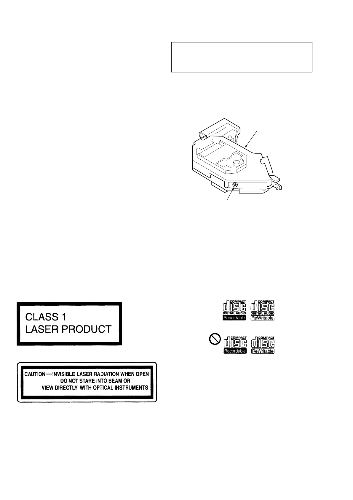
NOTES ON HANDLING THE OPTICAL PICK-UP BLOCK
OR BASE UNIT
The laser diode in the optical pick-up block may suffer electrostatic
breakdown because of the potential difference generated by the
charged electrostatic load, etc. on clothing and the human body.
During repair, pay attention to electrostatic breakdown and also use
the procedure in the printed matter which is included in the repair
parts.
The flexible board is easily damaged and should be handled with
care.
CAUTION
Use of controls or adjustments or performance of procedures
other than those specified herein may result in hazardous
radiation exposure.
If the optical pick-up block is defective, please replace the whole
optical pick-up block.
Never turn the semi-fixed resistor located at the side of optical
pick-up block.
optical pick-up bloc
semi-fixed resistor
NOTES ON LASER DIODE EMISSION CHECK
The laser beam on this model is concentrated so as to be focused on
the disc reflective surface by the objective lens in the optical pickup block. Therefore, when checking the laser diode emission, observe from more than 30 cm away from the objective lens.
Notes on Chip Component Replacement
• Never reuse a disconnected chip component.
• Notice that the minus side of a tantalum capacitor may be dam-
aged by heat.
• CDX-CA700/CA700X: AEP, UK model
This label is located on the bottom of the chassis.
TEST DISCS
This set can playback CD-R and CD-ROM discs. The following
test discs should be used to check the capability:
CD-R test disc TCD-R082LMT (Part No. J-2501-063-1)
CD-RW test disc TCD-W082L (Part No. J-2501-063-2)
Notes on CD-R/CD-RW discs
• You can play CD-Rs (recordable CDs)/CD-RWs (re writable CDs)
designed for audio use on this unit.
Look for these marks to distinguish CD-Rs/CD-RWs for audio
use.
These marks denote that a disc is not for audio use.
• Some CD-Rs/CD-RWs (depending on the equipment used for
its recording or the condition of the disc) may not play on this
unit.
• You cannot play a CD-R/CD-RW that is not finalized∗.
∗ A process necessary for a recorded CD-R/CD-RW disc to be
played on the audio CD player.
This label is located on the drive unit’s internal chassis.
SAFETY-RELATED COMPONENT WARNING!!
COMPONENTS IDENTIFIED BY MARK 0 OR DOTTED LINE
WITH MARK 0 ON THE SCHEMATIC DIAGRAMS AND IN
THE PARTS LIST ARE CRITICAL TO SAFE OPERATION.
REPLACE THESE COMPONENTS WITH SONY P ARTS WHOSE
PART NUMBERS APPEAR AS SHOWN IN THIS MANUAL OR
IN SUPPLEMENTS PUBLISHED BY SONY.
2
ATTENTION AU COMPOSANT AYANT RAPPORT
À LA SÉCURITÉ!!
LES COMPOSANTS IDENTIFIÉS P AR UNE MARQUE 0 SUR LES
DIAGRAMMES SCHÉMATIQUES ET LA LISTE DES PIÈCES
SONT CRITIQUES POUR LA SÉCURITÉ DE FONCTIONNEMENT.
NE REMPLACER CES COMPOSANTS QUE PAR DES PIÈCES
SONY DONT LES NUMÉROS SONT DONNÉS DANS CE MANUEL
OU DANS LES SUPPLÉMENTS PUBLIÉS PAR SONY.
Page 3
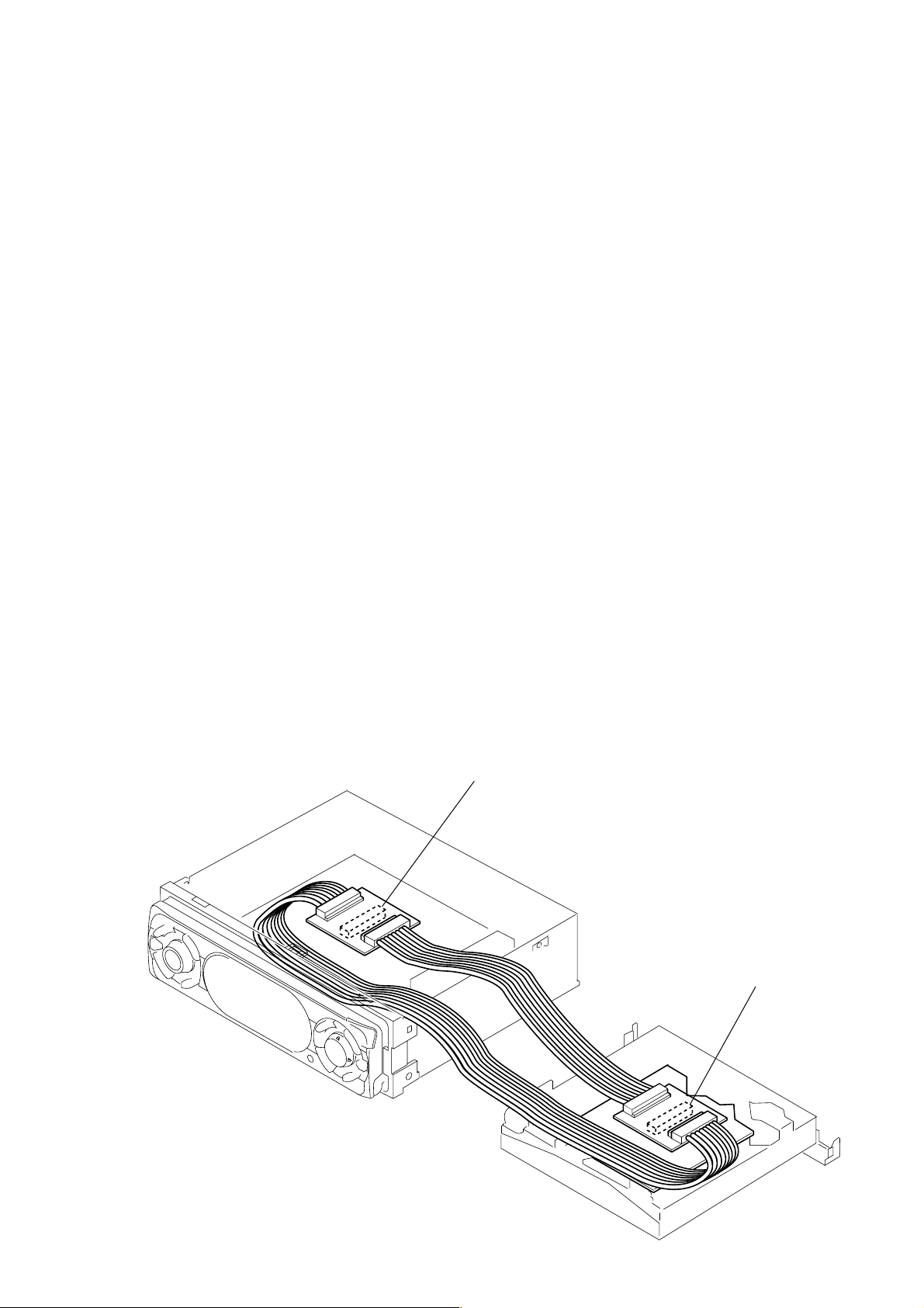
TABLE OF CONTENTS
CDX-CA700/CA700X
1. GENERAL
Location of controls (US, Canadian Model) ........................... 4
Location of controls (AEP, UK Model) ................................... 4
Connections (US, Canadian Model)........................................5
Connections (AEP, UK Model) ............................................... 6
2. DISASSEMBLY
2-1. Sub Panel Assy .................................................................... 7
2-2. CD Mechanism Block ......................................................... 8
2-3. Main Board ......................................................................... 8
2-4. Heat Sink ............................................................................. 9
2-5. Chassis (T.U) Assy .............................................................. 9
2-6. Disc In Board .................................................................... 10
2-7. Servo Board.......................................................................10
2-8. Shaft Roller Assy .............................................................. 11
2-9. Floating Block Assy .......................................................... 11
2-10. Optical Pick-up Block ....................................................... 12
3. DIAGRAMS
3-1. IC Pin Description............................................................. 13
3-2. Block Diagram –CD Section–...........................................15
3-3. Block Diagram –Tuner Section–.......................................16
3-4. Block Diagram –Display Section–.................................... 17
3-5. Circuit Boards Location .................................................... 17
3-6. Printed Wiring Boards –CD Mechanism Section–............ 18
3-7. Schematic Diagram –CD Mechanism Section– ................ 20
3-8. Schematic Diagram –Main Section (1/3)– ........................ 21
3-9. Schematic Diagram –Main Section (2/3)– ........................ 22
3-10. Schematic Diagram –Main Section (3/3)– ........................ 23
3-11. Printed Wiring Board –Main Section– .............................. 24
3-12. Printed Wiring Board –Relay Section– ............................. 26
3-13. Schematic Diagram –Relay Section–................................ 27
3-14. Printed Wiring Board –Key Section–................................ 28
3-15. Schematic Diagram –Key Section–................................... 29
4. EXPLODED VIEWS
4-1. Chassis Section ................................................................. 33
4-2. Main Board Section .......................................................... 34
4-3. Front panel Section ........................................................... 35
4-4. CD Mechanism Section (1) ............................................... 36
4-5. CD Mechanism Section (2) ............................................... 37
4-6. CD Mechanism Section (3) ............................................... 38
5. ELECTRICAL PARTS LIST ........................................39
EXTENSION CABLE AND SERVICE POSITION
When repairing or servicing this set, connect the jig (extension cable)
as shown below.
• Connect the MAIN board (CNP301) and the SER VO board (CN1)
with the extension cable (Part No. J-2502-062-1).
MAIN BOARD CNP301
SERVO BOARD CN1
3
Page 4
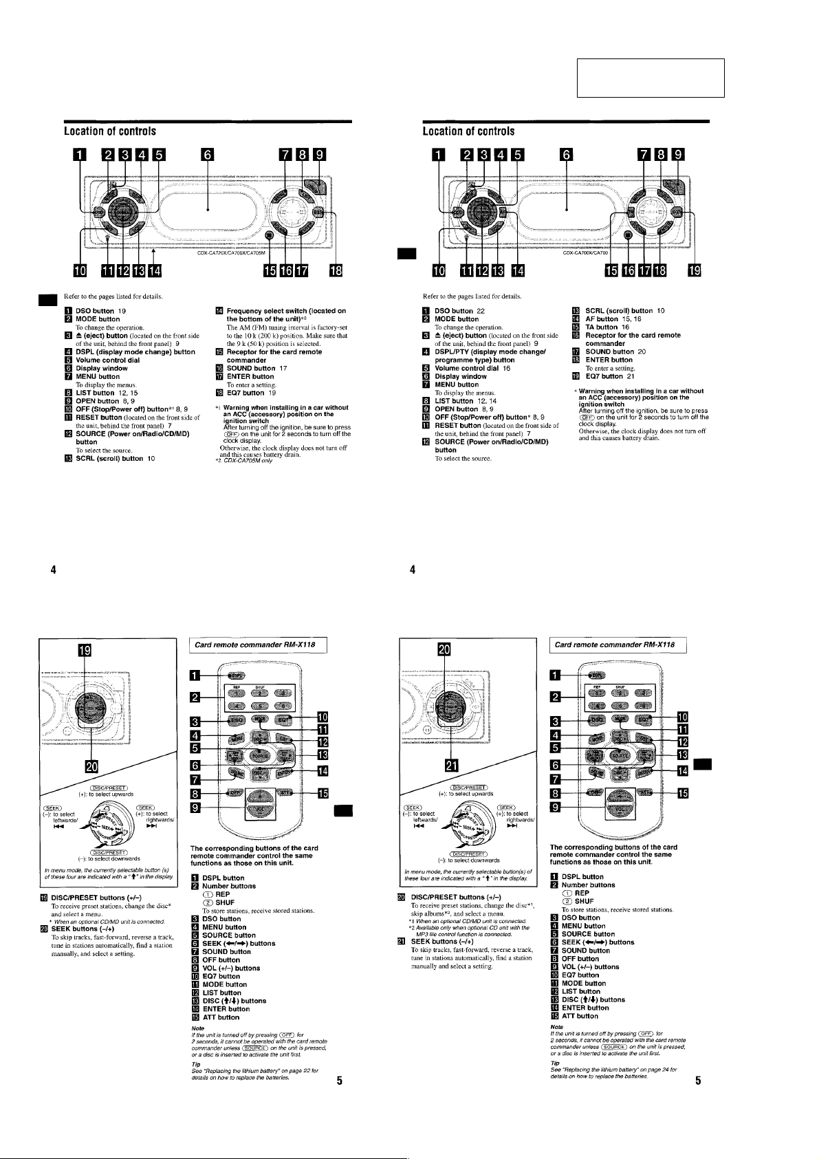
CDX-CA700/CA700X
(US, Canadian Model) (AEP, UK Model)
SECTION 1
GENERAL
This section is extracted
from instruction manual.
(US, Canadian Model) (AEP, UK Model)
4
Page 5
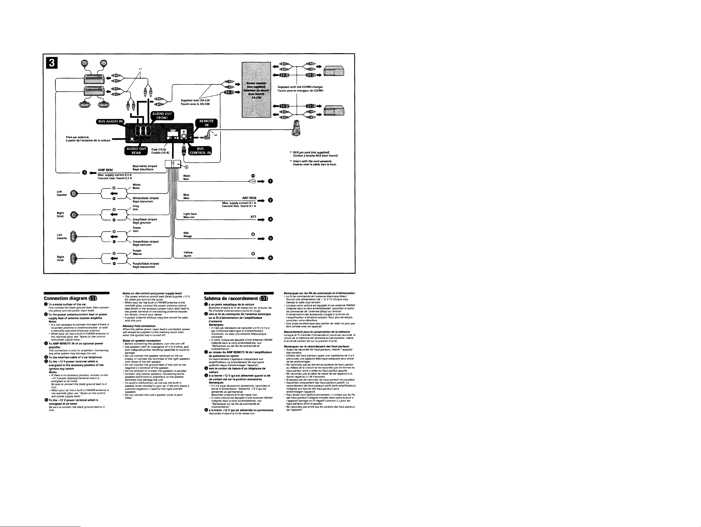
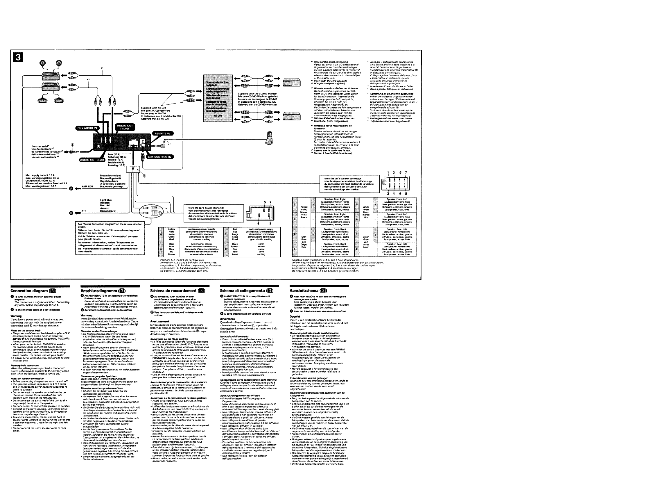
Connections (US, Canadian Model)
CDX-CA700/CA700X
55
Page 6
CDX-CA700/CA700X
Connections (AEP, UK Model)
66
Page 7
SECTION 2
W
DISASSEMBLY
Note : This set can be disassemble according to the following sequence.
SET
2-5. CHASSIS (T.U) ASSY
2-1. SUB PANEL ASSY
(Page 7)
(Page 9)
CDX-CA700/CA700X
2-2. CD MECHANISM BLOCK
(Page 8)
2-3. MAIN BOARD
(Page 8)
2-4. HEAT SINK
(Page 9)
2-6. DISC IN BOARD
(Page 10)
2-8. SHAFT ROLLER ASSY
(Page 11)
2-9. FLOATING BLOCK ASSY
(Page 11)
2-10. OPTICAL PICK-UP BLOCK
(Page 12)
Note : Follow the disassembly procedure in the numerical order given.
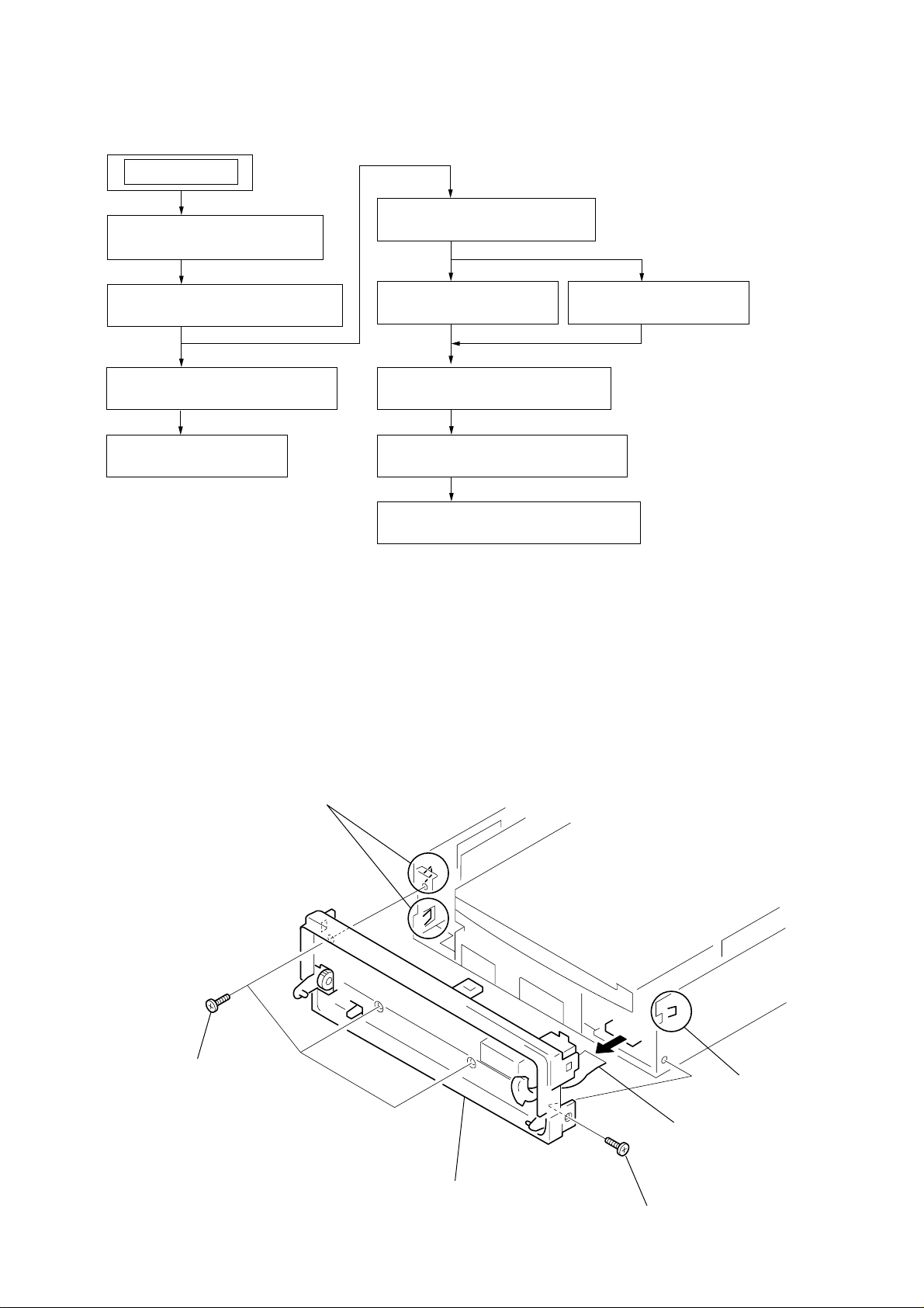
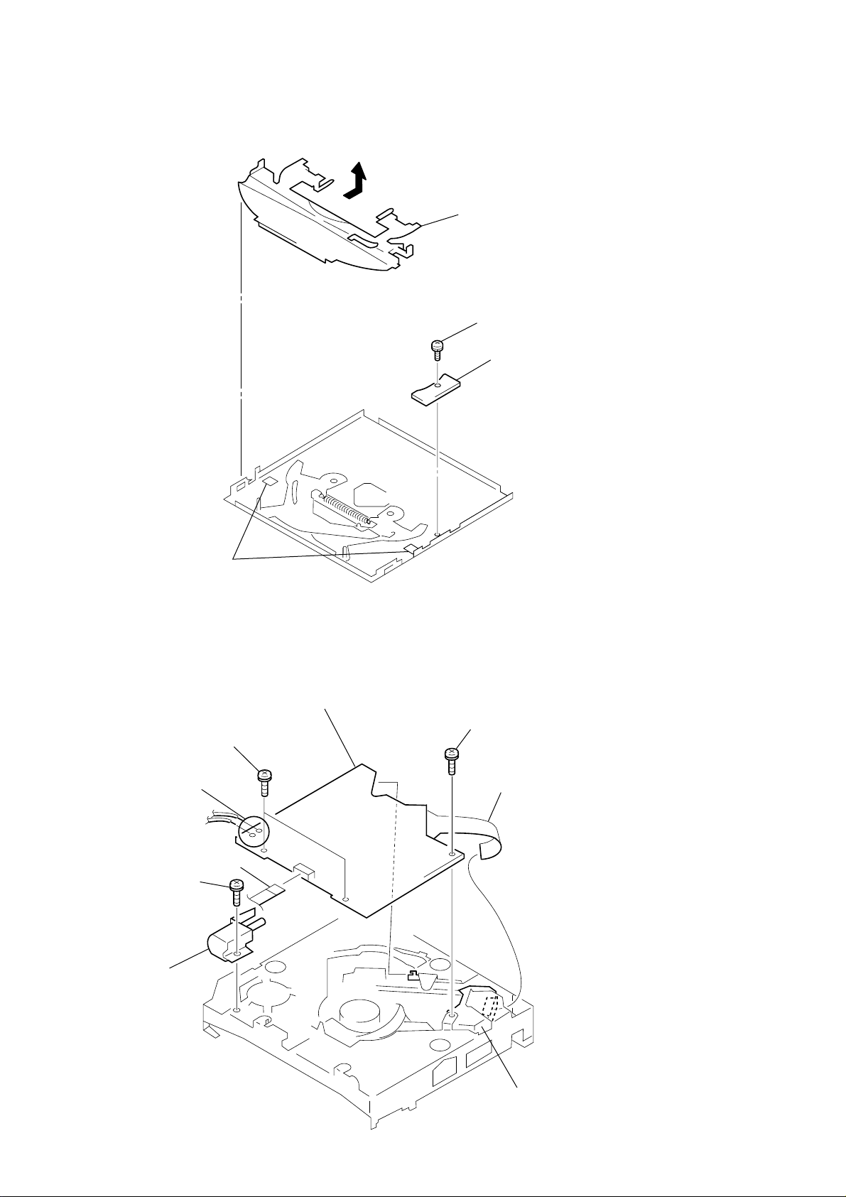
2-1. SUB PANEL ASSY
2-7. SERVO BOARD
(Page 10)
2
PTT 2.6x6
4
CLAWS
6
SUB PANEL ASSY
3
CLA
5
CN701
1
PTT 2.6x6
7
Page 8
CDX-CA700/CA700X
4
4
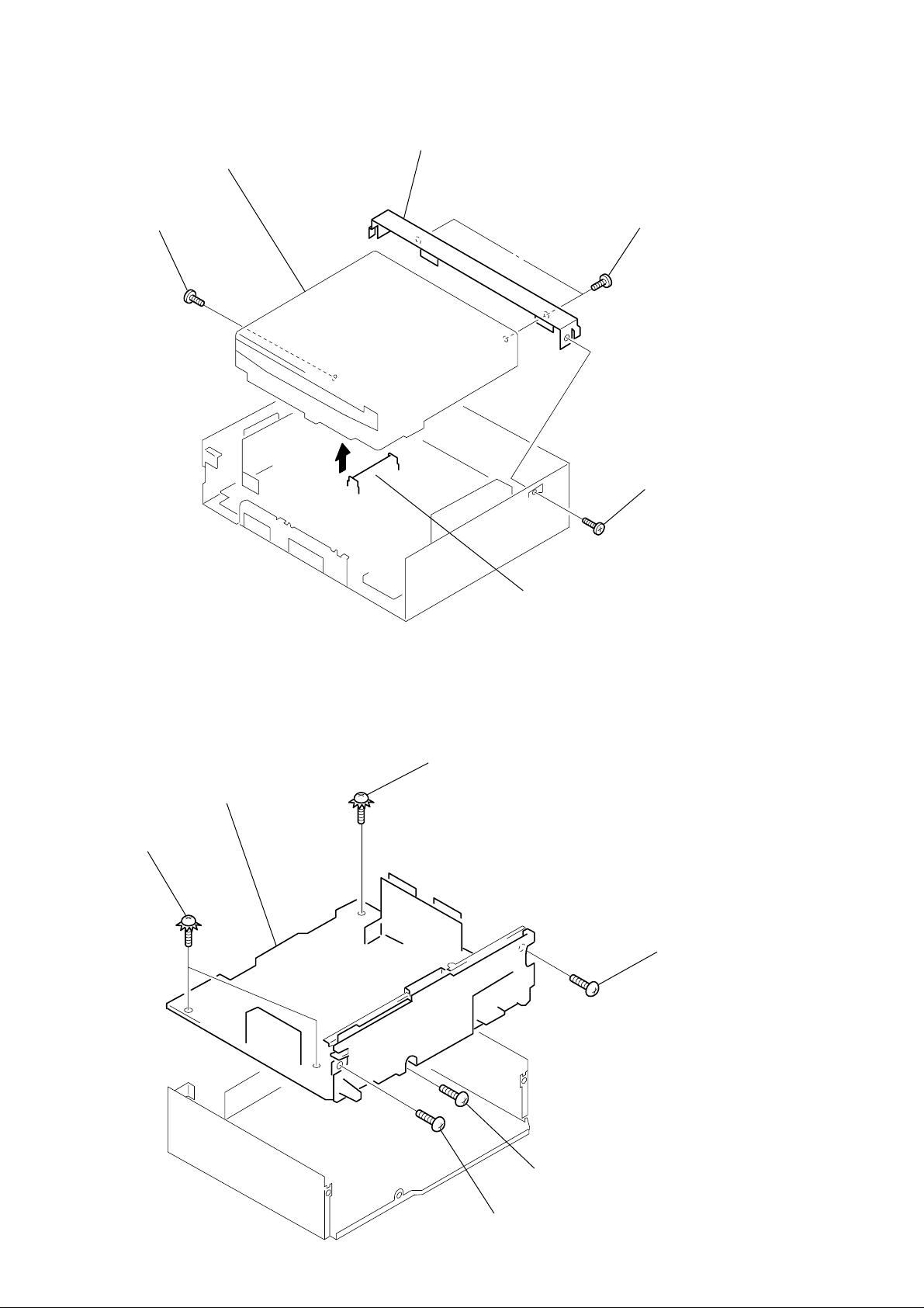
2-2. CD MECHANISM BLOCK
7
CD mechanism block
2
PTT 2.6x4
3
6
bracket (CD)
5
PTT 2.6x4
1
PTT 2.6x
2-3. MAIN BOARD
5
PTT 2.6x6
6
MAIN board
4
PTT 2.6x6
4
CNP301
1
PTT 2.6x
2
PTT 2.6x4
3
PTT 2.6x4
8
Page 9
y
2-4. HEAT SINK
0
CDX-CA700/CA700X
4
heat sink
3
PTT 2.6x1
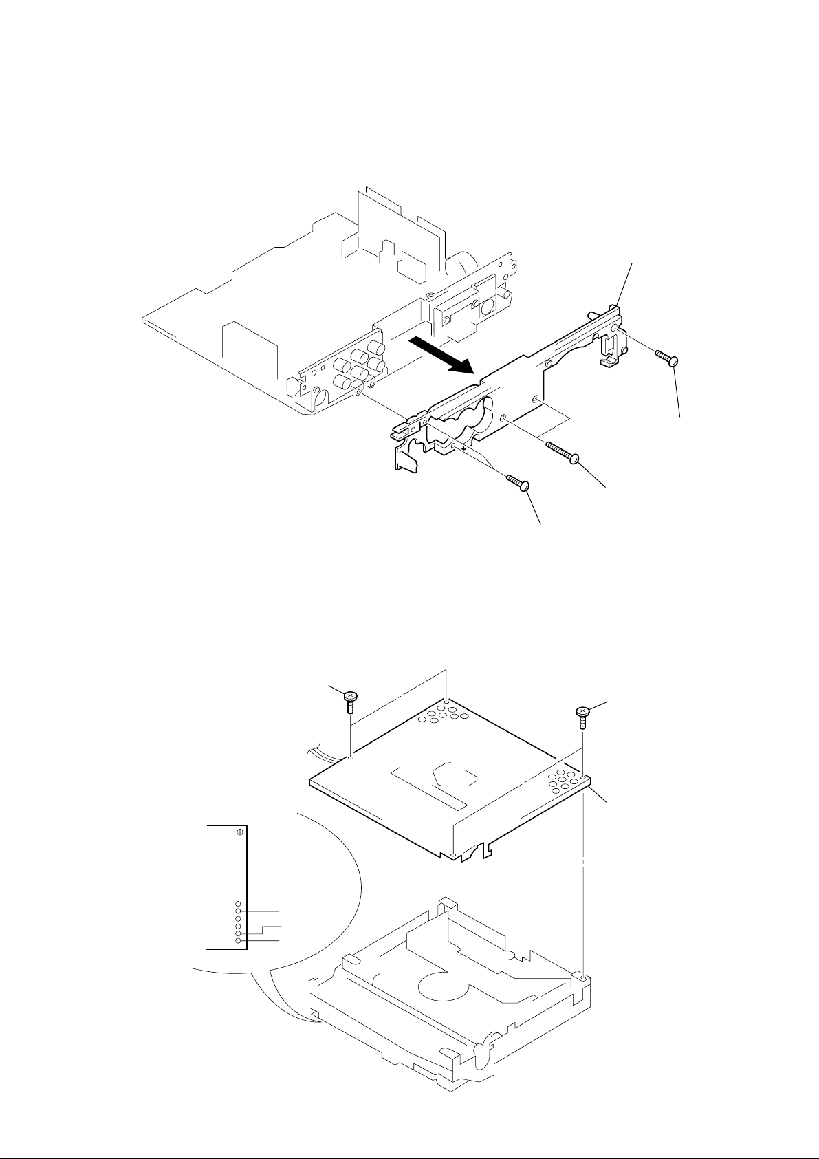
2-5. CHASSIS (T.U) ASSY
1
Unsolder the
lead wires.
2
P 2x3
1
PTT 2.6x10
2
PTT 2.6x16
3
P 2x3
4
chassis (T.U) sub ass
black
red
white
9
Page 10
CDX-CA700/CA700X
2-6. DISC IN BOARD
4
guide (disc)
1
PS 2x3
2
DISC IN board
2-7. SERVO BOARD
2
Removal the solders.
3
4
loading motor assy
P 2x3
3
claws
5
PS 2x4
1
CN3
7
SERVO board
6
PS 2x4
8
connector
10
optical pick-up block
Page 11
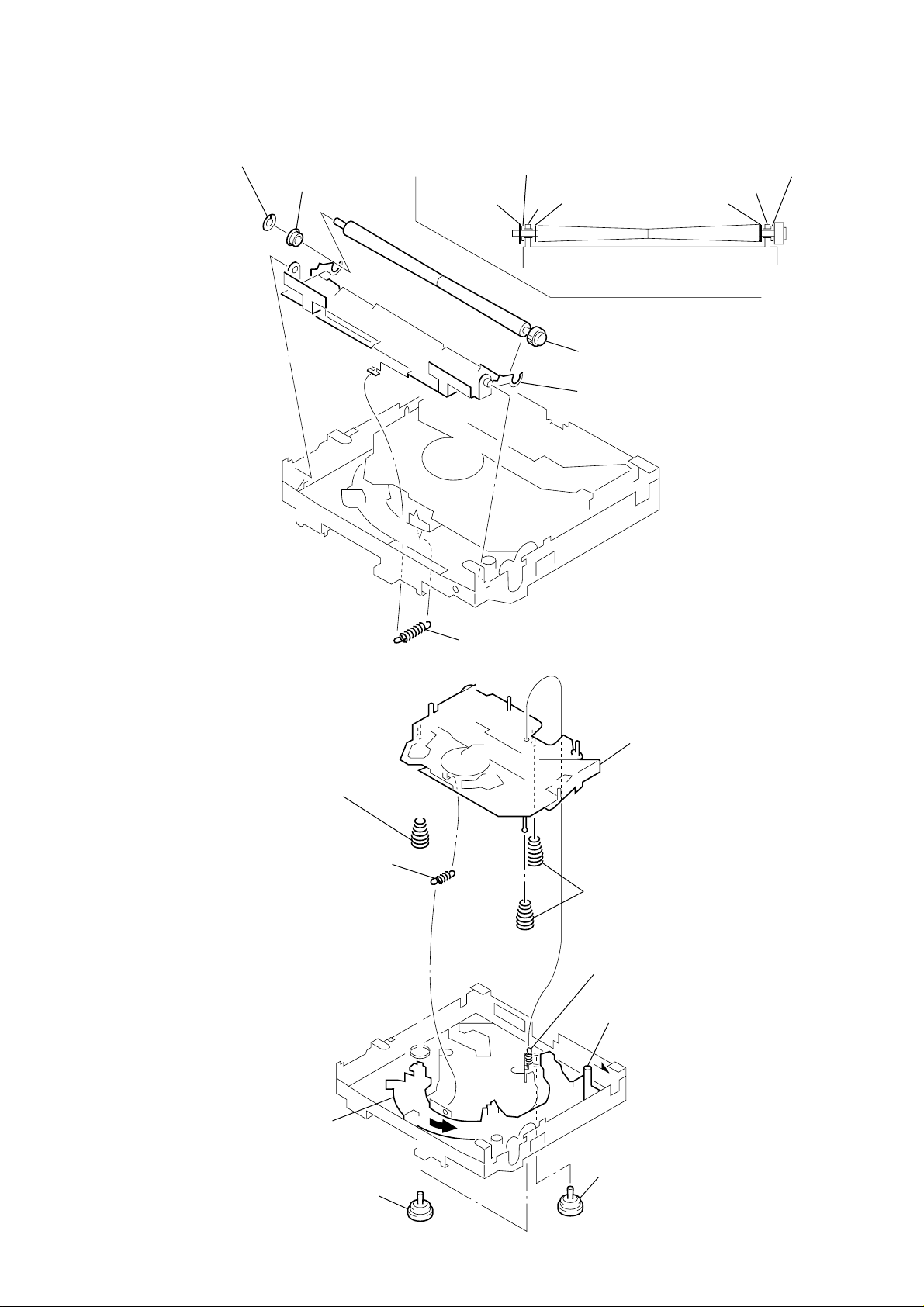
2-8. SHAFT ROLLER ASSY
• When installing, take note of the positions
arm (roller) and washers. (Fig. 1)
3
retaing ring (roller)
4
bearing (roller)
bearing (roller)
retaing ring (roller)
washer (RA)
arm
5
shaft roller assy
2
arm (roller T)
washer (RA)
Fig. 1
CDX-CA700/CA700X
bearing (roller)
arm
2-9. FLOATING BLOCK ASSY
8
compression spring (FL)
1
tension spring (KF1)
1
tension spring (RA3)
7
floating block assy
9
compression spring (FL)
2
tension spring (KR1)
5
Fit lever (D) in the
direction of the arrow.
6
Turn loading ring in the
direction of the arrow.
4
damper (T)
3
damper (T)
11
Page 12
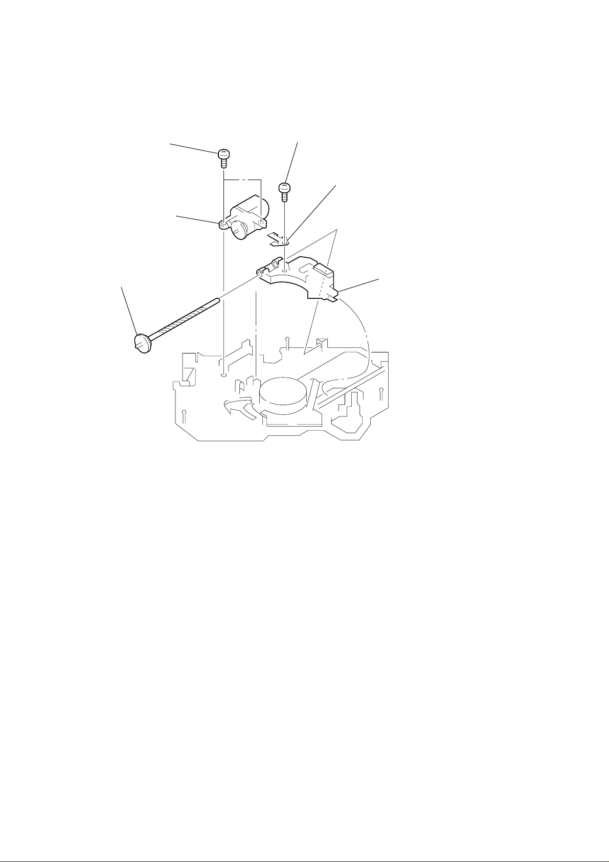
CDX-CA700/CA700X
2-10. OPTICAL PICK-UP BLOCK
1
P 2x3
2
sled motor assy
6
shaft (feed) assy
4
P 2x3
5
spring (feed), plate
3
optical pick-up block
12
Page 13
CDX-CA700/CA700X
SECTION 3
DIAGRAMS
3-1. IC PIN DESCRIPTION
• IC801 MN101C49KCY2 (SYSTEM CONTROL) (US, Canadian model)
• IC801 MN101C49KCX2 (SYSTEM CONTROL) (AEP, UK model)
Pin No. Pin Name I/O Pin Description
1 VREF– — Ground for A/D converter power supply
2 VSM I S-meter voltage detection signal input from tuner unit (TU10)
3 NIL I Connect to ground.
4 KEYIN1 I Key signal input
5 KEYIN0 I Key signal input
6 RC IN0 I Rotary commander key signal input from remote in jack (J561)
7 QUALITY I Noise detection signal input
8 NIL/MPTH I Connect to ground (US, Canadian)/Multi path detection signal input (AEP, UK)
9 DSTSEL/FUNCSEL I Destination set up detection signal input
10 VREF — A/D converter power supply
11 VDD — Power supply (+5 V) input pin
12 OSCOUT O High speed clock signal output (18.432 MHz)
13 OSCIN I High speed clock signal input (18.432 MHz)
14 VSS — Ground for power supply
15 XIN I Low speed clock signal input (32.768 kHz)
16 XOUT O Low speed clock signal output (32.768 kHz)
17 MMOD I
18 LCDSO O LCD serial data signal output to LCD driver (IC901)
19 LCDCE O LCD chip enable signal output to LCD driver (IC901)
20 LCDCKO O LCD serial clock signal output to LCD driver (IC901)
21 CD TSO O CD servo IC serial data signal output
22 CD TSI I CD servo IC serial data signal input
23 CD TCKO O CD servo IC serial clock signal output
24 SYSRST O System reset signal output to bus interface (IC581)
25 BUS ON O Bus on signal output to bus interface (IC581)
26 KEYACK I Key acknowledge detection signal input
27 NIL/DAVN I
28 BU IN I Back up power supply detection signal input
29 SIRCS I Remote signal input from remote control receiver (IC971)
30 CD SELFSW I CD mechanism self load position detection switch signal input from self switch (SW2)
31 CD PACK I CD text pack sync signal input from CD servo (IC1)
32 VDD2 — Power supply (+5 V) pin
33 RESET I microcomputer reset signal input from reset IC (IC551) “L”: reset
34 NOSE SW I Front panel attachment detection signal input from nose detect switch (S552) “L”: ON
35 BEEP O Beep signal output to power amp (IC751)
36 NCO O Not used. (Open)
37 TESTIN I Test mode detection signal input
38 ACCIN I Accessory power supply detection signal input
39 NCO (VCC) O Not used. (Open)
40 TELATT I Telephone ATT detection signal input
41 NCO (VCC) I Connect to power supply.
42 UNISO O Sony-Bus serial data signal output to bus interface (IC581)
43 UNISI I Sony-Bus serial data signal input from bus interface (IC581)
44 UNICKO O Sony-Bus serial clock signal output to bus interface (IC581)
45 I2C SIO I/O I2C bus serial data signal input/output
46 NCO O Not used. (Open)
47 I2C CKO O I2C bus serial clock signal output
48 NCO O Not used. (Open)
Memory mode select signal input (Input to “Low” (single chip mode).)
(Connect to ground.)
Connect to ground (US, Canadian)/RDS data block synchronization detection signal
input (AEP, UK)
Ver 1.1
13
Page 14
CDX-CA700/CA700X
Pin No. Pin Name I/O Pin Description
49 TUNON O Tuner power supply control signal output to power supply (IC601)
50 PW ON O System power supply control signal output to power supply (IC601)
51 TSTB O CD text parameter strob signal output to servo IC (IC1)
52 RFOK I RF OK signal input from servo IC (IC1)
53 CD RST O Reset signal output to servo IC (IC1)
54 A0 O
55 STB O Data strob signal output to servo IC (IC1)
56 X EN O Crystal oscillation control signal output Not used in this set.
57 LIMIT I CD Mechanism in-limit switch signal input from limit switch (SW3)
58 PH1 I CD Mechanism PH1 detection signal input Not used in this set.
59 D SW I CD Mechanism down switch signal input from down switch (SW5)
60 INSW/PH2 I CD Mechanism disc-in switch detection signal input from disc-in switch (SW1)
61 NC (PH3) I CD Mechanism PH3 detection signal input Not used in this set.
62 CD LM LO O CD Mechanism loading motor control signal output to loading motor drive (IC2)
63 CD LM EJ O CD Mechanism eject motor control signal output to loading motor drive (IC2)
64 4VPRE/NCO I/O Hi-Volt power selection “L”: with, “H”: without (US, Canadian)/open (AEP, UK)
65 PREOUTMENU/NCO I/O
66 AMPATT O Power amp ATT control signal output to power amp (IC751)
67 AMPON O Power amp standby control signal output to power amp (IC751)
68 CDMD ON O CD mechanism deck power supply control signal output
69 ATT O System ATT control signal output
70 VOLATT O Electrical volume ATT control signal output to electrical volume (IC331)
71 – 73 NCO O Not used. (Open)
74 MP3SEL I
75 SUB SEL I Sub-out function detection signal input “H”: without, “L”: with
76 SW SHIFT O Not used in this set. (Open)
77 COLSEL I Key illumination color selection detection signal input “L”: amber, “H”: green
78 NCO O Not used. (Open)
79 XCD ON O CD on signal output “H”: Play, “L”: Loading or standby
80 – 85 NCO O Not used. (Open)
86 E2P SIO I/O EEPROM serial data signal input/output
87 E2P CKO O EEPROM serial clock signal output
88 NCO O Not used. (Open)
89 FLASH W I Flash microcomputer write detection signal input “L”: Write mode
90 NIL/NS MASK O Connect to ground (US, Canadian)/Noise mask signal output (AEP, UK)
91 AD ON O Key power supply control signal output “L”: key active
92 DOORIND O Sub panel power supply control signal output
93 ILLON O Illumination power supply control signal output
94 DOOR SW I Front panel open/close detection signal input “L”: Close, “H”: Open
95 DAVSS — Ground pin
96 RE IN1 I Rotary encoder signal input from rotary encoder (RE901)
97 RE IN0 I Rotary encoder signal input from rotary encoder (RE901)
98 RC IN1 I
99 NCO O Not used. (Connect to ground.)
100 DAVDD — Power supply pin (+5 V)
Command/parameter identification signal output to servo IC (IC1)
“L”: Command, “H”: Parameter
Pre-out (4 V/5.5 V) menu selection “L”: with, “H”: without set up signal input
(US, Canadian)/open (AEP, UK)
MP3 control select signal input “L”: MP3 CD changer control correspondence,
“H”: not correspondence
Rotary commander shift key signal input from remote in jack (J561)
“L”: Shift key on
14
Page 15
3-2. BLOCK DIAGRAM — CD SECTION —
OPTICAL PICK-UP
KSS-720A
RF AMP,DIGITAL SERVO
DIGITAL SIGNAL PROCESSOR
IC1
CDX-CA700/CA700X
PD
LD
A
C
B
D
E
F
FOCUS
COIL
I-V
CONV.
LD
DRIVE
Q1
A
84
C
85
B
82
D
83
E
87
F
86
PD
97
A+5V
LD
98
FOCUS/TRACKING COIL DRIVE,
SLED/SPINDLE/LOADING MOTOR DRIVE
FCS-
15
FCS+
16
APC
IC2
FOCUS
COIL
DRIVE
TRACKING
ERROR
(Page 16)
TUNER
LOUT
RF
EQ
FORCUS
ERROR
FD
26
EFM
DEMOD
SERVO
CTL
FDTDSD
62 63 64 65
MD
D/A
CONV
DSUB CODE
PROCESS
I/F
OSC
23 24
X1
16.9344MHz
ROUT
PACK
TSTB
TSCK
TSI
SCK
STB
RST
RFOK
XTALEN
16
12
R-CH
52
56
55
54
SI
8
SO
7
6
5
AO
4
3
2
9
SW5
(DOWN)
CDL
SECTION
A
SYSTEM CONTROL
31
CD_PACK
51
TSTB
21
CD_TSO
22
CD TSI
23
CD TCKO
55
STB
54
AO
53
CD_RST
52
RFOK
59
D SW
IC501(1/3)
TRACKING
COIL
M902
(SLED)
M901
(SPINDLE)
M903
(LOADING)
30
CD_SELFSW
INSW/PH2
60
57
LIMIT
CD_LM _LO
62
63
CD_LM_ EJ
68
CDMD ON
79
XCD ON
RESET
IC551
33
1
S551
(RESET)
RESET
2
BU+5.8V
• Signal path
:CD
• R-ch is omitted due to
same as L-ch.
(DISC IN)
CDMD ON
SWITCH
Q352
BATT
SW2
(SELF)
SW1
SW3
(LIMIT)
CD ON
SWITCH
Q353
TRK+
17
TRK-
18
SL-
M
13
SL+
14
SP-
M
11
SP+
12
LD-
M
9
LD+
10
TRACKING
COIL
DRIVE
SLED
MOTOR
DRIVE
SPINDLE
MOTOR
DRIVE
LOADING
MOTOR
DRIVE
TD
23
SD
5
MD
6
LOAD
1
EJECT
2
A+5V
AU+5V
D+5V
DR+6V
CD+5V
REG
Q350,D350
CD DRIVE+6V
REG
Q351,D351
D352
15 15
Page 16

CDX-CA700/CA700X
A
3-3. BLOCK DIAGRAM — TUNER SECTION —
TUNER UNIT
TU10
J10
(ANTENNA)
2
1
ANTFM
ANTAM
MPX
AM DET
S-METER
I2C SDA
I2C SCL
E2PROM SDA
E2PROM SCL
RDS DET
10
8
14
12
13
17
18
9
NOISE AMP
BUFFER
Q21
AEP,UK MODEL
X51
4.332MHz
(Page 15)
AEP,UK MODEL
IC20
MPX
16
OSCD
4
OSCI
5
SECTION
NOISE
SUPPRESSOR
D21,22
MS MASK
SWITCH
Q22
RDS DECODER
IC51
CD
LVIN
SDA
SCL
MPTH
DAVN
PJ151
L
-5
-6
-1
-2
-3
-4
1
9
2
10
4
12
3
11
13
7
15
5
6
8
16
FL+
FL-
RL+
RL-
FR+
FR-
RR+
RR-
ATT
ACC
TEST
AMP R
ANT R
GND
+B (BATT)
BUS AUDIO IN
R
L
AUDIO OUT FRONT
R
L
AUDIO OUT REAR
R
ELECTRONIC VOLUME
IC331
ACOUT RCH
ACOUT LCH
AUX-LCH
4
CDRR-CH
CDL
CA700
BU+5V
20
9
10
2
8
MD RCH
42
MD LCH
43
MPX1
12
AM/MPX2
9
LEVEL
13
MPIN
14
SDA
19
SCL
20
EXA-ATT
17
SYSTEM CONTROL
QUALITY
7
VOL ATT
70
MS MASK
90
VSM
2
I2C SIO
45
I2C CKO
47
DSTSEL/
9
FUNCSEL
E2P SIO
86
E2P CKO
87
8
MPTH
27
DAVN
IC501 (2/3)
ACIN RCH
OUT FL
OUT RL
OUT FR
OUT RR
ATT
BEEP
AMP ON
AMP ATT
TEL ATT
ACC IN
TEST IN
TUN ON
PW ON
SYSRST
BUSON
UNISI
UNICKO
UNISO
BU IN
36
38
35
28
27
26
27
69
35
67
66
40
38
37
49
50
24
25
43
44
42
28
R-CH
L-CH AMP
R-CH
IC332
13
12
8
11
9
10
MUTE
Q181
LINE MUTE
CONTROL
Q621,622
BUS INTERFACE
IC581
RST
BUSON
DATA OUT
CLK IN
DATA IN
B/U-C
BUSON
DATA I/O
CLK
RST
BATT
MUTE
Q171
R-CH
D621
DELAY BATT
1
6
4
2
3
MUTE
Q185
Q581,D584,585
BATT DET
D624
AEP,UK MODEL
CNJ581
BUS
CONTROL IN
6
5
4
BATT
MUTE
Q175
D626
TUN-ON SW
2
STB
4
8
3
2
1
7
BATT
AEP,UK
MODEL
MUTE
Q625
D625
POWER SUPPLY
IC601
AMP+B
ANT+B
BU+B(5.8V)
COM8.7V
TU+B(5.1V)
TU+B(8.4V)
ACC
DETECT
Q571
VCC
POWER AMP
IC751
12
11
AUX
16
STBY
4
MUTE
22
TEL
ATT
Q585
6
8
5
9
10
11
7
D613
D612
BU+5.8V
COM+8V
TU+5V
TU+8.5V
BATT
R-CH
R-CH
R-CH
CNP781
5
3
9
7
R-CH
BATT
F901
10A
19
17
18
• Signal path
: FM
: AM/MW/LW
: CD
• R-ch is omitted due to same as L-ch.
1616
Page 17

CDX-CA700/CA700X
t
3-4. BLOCK DIAGRAM — DISPLAY SECTION —
SYSTEM CONTROL
5
4
26
91
98
6
29
34
92
15
16
IC501 (3/3)
KEY IN0
KEY IN1
KEY ACK
AD ON
RC IN1
RC IN0
SIRCS
NOSESW
DOORIND
XIN
XOUT
KEY MATRIX
LSW902,904,905,907,
911,913,915,916,918,919
S901,903,912,914,917
LSW906,910
CA700/CA700X:AEP,UK MODEL
J561
(REMOTE IN)
LED801
(CD WINDOW)
LSW801(2/2)
LSW801(1/2)
Z
D702
Z
D701
D553
REMOTE
RECEIVE
S552
(NOSE)
DOOR IND
SWITCH
Q631
KEY
ACTIVE
Q551
IC971
X502
32.768kHz
LCD SO
LCD CKO
LCD CE
ILL ON
OSC OUT
OSC IN
3-5. CIRCUIT BOARDS LOCATION
LCD DRIVE
IC901
DATA
100
99
98
ILL ON
SWITCH
Q603
BATT
X501
18.432MHz
LCD DATA
CLK
LCD CLK
CE
LCD CE
SEG84
ILL B+
REG
Q601
SEG1
COM1
COM4
3
|
|
86
LCD
LCD901
90
|
|
87
ILL+5V
CA700
LED
DRIVE
1
Q902
LED
DRIVE
2
Q901
ILL+5V
CA700X
LED931,941
LCD BACK
()
LIGHT
LSW902,904,905,907,
911,913,915,916,918,919
LED901,912,917
LSW906,910
CA700/CA700X:AEP,UK MODEL
()
ILLUMINATION
ILL+5V
LED903,914
KEY
()
ILLUMINATION
KEY
SUB (CD) board
KEY board
• Waveforms
— Servo Board —
(MODE: CD PLAY)
1
18
20
19
93
12
13
DISC IN board
1.8Vp-p
SUB board
LIMIT board
tuner uni
(TU10)
MAIN board
SERVO board
— Main Board —
1
3.4Vp-p
ROTARY
ENCODER
RE901
REIN0
97
REIN1
96
2
3
16.9344MHz
IC1
3.3msec
IC1
IC1
(XTAL)
wd
(PACK)
ts
uj
(RFO)
5Vp-p
1.5Vp-p
2
3
IC51
IC501
IC501
4.332MHz
(OSC O)
4
18.432MHz
(OSCOUT)
qs
32.768kHz
(XOUT)
qh
1.8Vp-p
5.2Vp-p
4
0V
Approx. 100mVp-p
oa
(FEO)
IC1
5
Approx. 100mVp-p
od
(TEO)
IC1
0V
17 17
Page 18

CDX-CA700/CA700X
3-6. PRINTED WIRING BOARDS — CD MECHANISM SECTION — • Refer to page 17 for Circuit Boards Location.
THIS NOTE IS COMMON FOR PRINTED WIRING
BOARDS AND SCHEMATIC DIAGRAMS.
(In addition to this, the necessary note is
printed in each block.)
for schematic diagram:
• All capacitors are in µF unless otherwise noted. pF: µµF
50 WV or less are not indicated except for electrolytics
and tantalums.
• All resistors are in Ω and 1/
specified.
• % : indicates tolerance.
f
•
• C : panel designation.
Note:
The components identified by mark 0 or dotted
line with mark 0 are critical for safety.
Replace only with part
number specified.
• A : B+ Line.
• Power voltage is dc 14.4V and fed with regulated dc power
• Voltages are taken with a VOM (Input impedance 10 MΩ).
• Waveforms are taken with a oscilloscope.
• Circled numbers refer to waveforms.
• Signal path.
: internal component.
supply from ACC and BATT cords.
Voltage variations may be noted due to normal produc-
tion tolerances.
Voltage variations may be noted due to normal production tolerances.
F : FM
f : AM/MW/LW
J : CD
4
W or less unless otherwise
Note:
Les composants identifiés par
une marque 0 sont critiques
pour la sécurité.
Ne les remplacer que par une
piéce portant le numéro
spécifié.
234567891011121314
1
A
B
C
D
E
F
for printed wiring boards:
• X : parts extracted from the component side.
• Y : parts extracted from the conductor side.
• x : parts mounted on the conductor side.
a
•
• : Pattern from the side which enables seeing.
Caution:
Pattern face side: Parts on the pattern face side seen from the
(Side B) pattern face are indicated.
Parts face side: Parts on the parts face side seen from the
(Side A) parts face are indicated.
: Through hole.
(The other layer’s patterns are not indicated.)
G
H
SW5
I
J
1818
Page 19

CDX-CA700/CA700X
A
B
C
D
E
1
234567891011121314
• Semiconductor
Location
Ref. No. Location
IC1 E-7
IC2 H-7
Q1 C-6
TP66
TP64
TP47
R21
TP48
TP56
TP76
R22
TP52
TP61
TP74
TP50
TP58
C71
TP51
TP62
CN1
TP7
TP59
TP72
TP63
TP80
TP60
TP71
R19
TP77
R26
C4
TP8
R17
TP9
TP78
Q1
C6
TP70
C27
R30
R3
C25
C34
R18
C41
C3
TP79
C29
C5
C1
R29
C16
C17
TP11
C9
C8
C43
C10
TP12
C70
C15
IC1
TP82
TP81
TP83
C11
TP89
C14
C13
C18
C24
R9
R5
C20
TP23
TP84
TP10
(Page 25)
C19
C23
R8
TP22
TP24
TP25
TP88
F
G
H
TP20
X1
R7
R6
TP17
TP92
C22
TP16
C36
TP34
TP35
TP36
TP46
C38
IC2
TP39
BP2
TP37
TP38
TP41
TP40
TP31
TP30
TP45
TP42
BP1
TP27
C35
TP44
TP43
TP32
R12
C30
TP28
TP33
R15
R10
TP29
TP15
TP21
TP26
BP3
TP2
R14
TP14
BP4
TP18
TP1
TP5
TP4
TP6
TP3
TP75
TP69
TP68
TP57
R20
TP73
TP53
TP86
TP87
I
TP54
FB5
C44
R31
TP49
TP85
C26
TP55
TP91
TP90
TP19
CN3
J
19 19
Page 20

CDX-CA700/CA700X
• Refer to page 17 for Waveforms.
3-7. SCHEMATIC DIAGRAM — CD MECHANISM SECTION — • Refer to page 30 for IC Block Diagrams.
CN2
SW3
TP77
TP78
C1
TP81
TP82
TP83
TP84
C5
R29
R30
TP79
TP80
C43
Q1
C3
TP9 TP8
R26
R3
C4
C6
C14
TP10
C13
C11
R5
TP7
TP12
TP11
C15
C10
C9
TP89
C18
C19
C20 C23
R9
C24
TP23
TP22
TP25
TP24
R8
TP88
IC1
C35
TP45
TP44
TP43
TP42
TP41
TP40
TP39
TP38
TP37
TP46
TP36
C38
CN1
M902
M901
SW2
SW1
Note:
• Voltage is dc with respect to
ground under no-signal conditions.
no mark : CD PLAY
TP4
TP2
TP3
M903
CN3
SW5
TP93
TP94
TP95
TP96
TP97
TP98
TP1
TP5
TP85
TP92
TP87
TP86
C8
TP35
TP34
C16C70
BP1
C29
R14
C25
C34
X1
C71
TP33
BP2
TP32
IC B/D
C17
C41
C27
C26
C30
R12
R10
TP31
TP30
R15
TP90
TP91
TP27
TP29
TP26
TP28
R7
TP15
TP21
BP3
TP18
TP17
TP20
TP16
TP19
C22
IC2
TP14
BP4
R6
C36
R31
C44
FB5
R22
R21
R18
R19
R20
R17
TP66
TP61
TP76
TP60
TP75
TP59
TP74
TP58
TP73
TP57
TP72
TP56
TP71
TP55
TP70
TP54
TP69
TP53
TP68
TP52
TP51
TP50
TP64
TP49
TP48
TP63
TP47
TP62
CN1
(Page 23)
IC B/D
2020
Page 21

• Refer to page 17 for Waveform.
3-8. SCHEMATIC DIAGRAM — MAIN SECTION (1/3) —• Refer to page 30 for IC Block Diagrams.
CDX-CA700/CA700X
J10
R18
C18
R21
Q21
R19
C10
C21
R23
R25
C11
R24
C22
C29
C25 R26 R27
C15
C14
C23
R10
R22
C26
C24
TU10
C13
IC20
D22
C28
D21 Q22
C27
R29
R28
R13
R14
D23
C16
C17
R31
C41 C42
C31
R334 R335 R336
IC332 IC333
C339
C33C32
R332R333
C306
C307 C335
R32R41
C337
C338
R339 R340 R341
C342
C340
R337
C343
R338
C341
R344
R343
C344
IC B/D
C241
C141
C336
IC331
R170
R180
R270
R280
(Page 22)
IC51
IC B/D
C63
C62 C58
C61
C59
R54
X51
C54
C56
C55
C57
R57
C53
R60
R56
(Page 23)
C330
R330
C331 C333
R345
C334
Note:
• Voltage is dc with respect to ground under
no-signal (detuned) condition.
no mark : FM
( ) : AM/MW/LW
21 21
Page 22

CDX-CA700/CA700X
3-9. SCHEMATIC DIAGRAM — MAIN SECTION (2/3) — • Refer to page 32 for IC Block Diagram.
(Page21)
R272
R282
R172
R429
R431
R435
R433R182
C273
R276
R286
C283
C173
R176
R186
C183
Q622
Q271
Q281
Q171
Q181
R184
Q621
R274
R284
R174
R175
D621
C623
R275
R285
R185
R622
R448
R462
R464
R453
Q275
Q285
Q175
Q185
R629
C192
C627
C277
C292
C185
D625
R191
Q625
R281
R291
R181
C276
C286
C176
C186
R283
R293
R183
R193
R690
C753
R279
R289
R179
R189
C755
R751
R754
C279
C287
C177
C187
R753
R752
IC751
C752
C757 C756
D721
D731
D722
D732
D723
D733
D724
D734
R143
R243
R142
R242
C178
C278
C188
C288
C142
C242
PJ151
CNP781
R574
R626
C551
R616
D552
C615
C614
R588
IC601
Q585
C613
R589
IC B/D
C611C610
C612
R591
R590
(Page23)
Q571
R571
D613
D612
R572
C573 C571
D614 D611
R576
R575
R573
R782
D782
D781
R787
R610
C785
C787 C786
C781
C783C782
F901
C784
L781
Note:
• Voltage is dc with respect to ground under
no-signal (detuned) condition.
no mark : FM
( ) : AM/MW/LW
2222
Page 23

• Refer to page 17 for Waveforms.
3-10. SCHEMATIC DIAGRAM — MAIN SECTION (3/3) — • Refer to page 32 for IC Block Diagram.
CDX-CA700/CA700X
Ver 1.1
C350
CNJ581
C302
R356
C305
R355
D350
R350
R351
C301
Q350
C351
C352
(Page20)
CNP301
R352
R353
R354
C353
C354
R586
D585
R585
TH501
D584
Q351
Q581
D582
R583
R584
D352
D351
D581
Q352
Q353
R357
C303
IC B/D
IC581
C581
(Page21)
R12
R508
R507
C506
R515
C507
R527
R526
C501
R531
R500
R502
C514
R511
R509
R510
R506
R505
R504
R501
IC551
R532
X502
C511
C505
C504
C513
X501
C510
R528
R529
R551
R503
Q601
R602
R635
D703
C703
R603
R606
R615
R712
D553
R601
R604 R605
R607 R608 R609
S552S551
R543
R542
Q551
R512
R513
R514
R517
R519
R555
R560
R566
R538
R565
R536
R525
R524
R521
2
2
IC501
R541
R592
R556
R557
(Page22)
R630
Q603
D712 D710
R719
R710
R711
R715
R714
R713
D711
R702
D702
R561
R563
R564
R701
R631
R632
R633
R634
R716
R562
D701
R720
R721
R722
R723
R724
R725
R726
R727
R728
R729
R730
Q631
(Page27)
CN701
J561
Note:
• Voltage is dc with respect to ground under
no-signal (detuned) condition.
no mark : FM
( ) : AM/MW/LW
< > : CD PLAY
23 23
Page 24

CDX-CA700/CA700X
3-11. PRINTED WIRING BOARD — MAIN SECTION — • Refer to page 17 for Circuit Boards Location.
• Semiconductor Location
Ref. No. Location
(D21) F-3
(D22) F-3
(D23) F-2
D350 H-10
D351 G-10
D352 G-10
D552 F-9
D553 G-7
D581 D-9
D582 D-9
D584 E-9
D585 E-9
D611 F-9
D612 F-9
D613 E-9
D614 E-9
D621 D-8
D625 D-7
D701 I-3
D702 I-3
D703 J-3
D710 I-2
D711 I-2
D712 I-2
D721 C-7
D722 C-7
D723 C-7
D724 C-7
D731 C-7
D732 C-7
D733 C-7
D734 C-7
D782 D-8
( ): AEP, UK Model only
Ref. No. Location
(IC20) E-2
(IC51) H-2
IC331 F-4
IC332 F-5
IC333 F-5
IC501 H-6
IC551 I-9
IC581 D-9
(Q21) E-2
(Q22) F-2
Q171 C-4
(Q175) D-6
Q181 C-3
(Q185) D-6
Q271 C-4
(Q275) C-5
Q281 C-4
(Q285) C-6
Q350 H-10
Q352 G-9
Q353 G-9
Q551 H-4
Q571 G-8
Q581 E-9
Q585 F-8
Q601 H-10
Q603 H-10
Q621 D-7
Q622 D-7
Q625 D-6
Q631 I-9
C353
C350
D350
R630
C354
C351
Q350
C783
D351
R551
D352
R352
R351
Q603
Q601
R631
D582
D581
C782
R586
R585
D613
D612
R626
R353
R350
R357
R356
R355
Q631
IC551
R354
R615
C506
R583
D585
D584
D552
Q353
R584
Q352
C784
R634
C581
IC581
Q581
D614
R635
R515
R575
R588
R589
C571
C573
R503
R576
D611
Q585
R573
R571
R610
R574
R592
C785
R590
R591
Q571
R787
R782
R543
C786
D782
R572
R563
R542
D722 D721 D731
C787
D621
R622
Q621
R753
R508
R562
R601
R603
R602
R604
R606
R605
R607
R609
R608
R632 R633
R531
R532
D732
Q622
C505
C627
R752
C504
R504
R529
D733
D723
D734
D724
R751
R528
D625
R505
C755
D553
R564
R500
C513
C514
R510
R690
R754
R506
C757
C756
R501
C501
R509
R629
R502
R511
C507
C511
C177
Q625
R561
R521
C187
R179
C176
R193
R189
C186
Q185
Q175
R556
Q285
IC501
R289
C286
R191
R12
C287
C279
R279
R183
R181
C185
R332
R333
C337
R337
R338
C341
R293
C276
R283
R291
C292
C192
R281
C342
R344
R525
Q275
C338
C339
C340
C277
R464
R453
R343
R536
R462
R448
R524
R334
R538
R514
R513
R512
IC332
IC333
R339
R555
C278
Q271
C343
R274
R276
R336
R335
C344
R341
R340
R566
R519
R517
R565
R275
Q171
R176
R429
R272
R560
R541
R507
R175
R431
R270
R719
C178
R174
R282
R280
IC331
R557
R712
R286
C336
Q281
R713
R170
Q551
C703
C288
R284
R715
R526
R172
R180
C331
R714
R285
R186
R433
R345
R527
R435
R182
R711
R710
D703
R185
R184
C333
D701
D702
R701
R702
C330
C33
C188
R330
Q181
R243
R32
R716
R143
C42
C32
R721
C242
R242
R27
C26
C27
D22
R21
C21
C22
C25
R26
D21
C55
C54
R54
R723
R142
R41
C31
R725
C41
R31
R616
C142
R23
R19
C24
C28
C63
D712
R727
C18
IC20
R28
R18
R29
C62
C23
R22
D23
C61
C53
234567891011121314
Q21
R729
C59
Q22
C58
C56
R728
R726
R25
R24
C29
D711
D710
R724
C10
C13
R14
C17
R57
R722
C11
C15
R60
R730
R720
R13
C57
IC51
1
A
B
C
D
E
R10
F
G
H
R56
I
J
2424
Page 25

CDX-CA700/CA700X
A
B
C
D
1
J10
TU10
234567891011121314
PJ151
J561
US,Canadian Model
CNP781
C781
D781
CNJ581
L781
AEP Model
TH501
C14
C183
C283
C173
IC751
C752
C273
C623
E
F
G
H
C611
C613
C614
C352
C610
C612
C615
IC601
Q351
• Semiconductor
Location
Ref. No. Location
D781 D-9
C16
C334
C141
C241
C335
C307
C306
C303
CNP301
C302
C305
C301
C753
IC601 E-10
IC751 B-6
C510
X51
X501
I
CN701
X502
C551
Q351 G-10
S552
J
S551
(Page 19)(Page 26)
25 25
Page 26

CDX-CA700/CA700X
3-12. PRINTED WIRING BOARD — RELAY SECTION — • Refer to page 17 for Circuit Boards Location.
A
B
C
D
1
LSW801
234567891011121314
LED801
E
F
G
H
(Page 25)
CNP802
CNP801
I
(Page 28)
J
2626
Page 27

3-13. SCHEMATIC DIAGRAM — RELAY SECTION —
CDX-CA700/CA700X
(Page 23)
CNP802
LSW801(1/2)
LED801
LSW801(2/2)
CNP801
(Page 29)
27 27
Page 28

CDX-CA700/CA700X
3-14. PRINTED WIRING BOARD — KEY SECTION — • Refer to page 17 for Circuit Boards Location.
A
B
C
D
1
LSW915
S914
LED914
S917
LED917
234567891011121314
LED912
S912
LSW916
LSW911
LSW913
LSW919
LSW918
IC971
LSW910
LED941
LCD901
LED931
LSW907
LSW906
LSW905
S901
LED901
LSW902
S903
LED903
LSW904
E
F
G
H
R935
R934
R932
R916
R931
R917
R915
R918
R930
R914
R913
R982
R952
R953
R912
R919
R951
R958
CN901
R911
R950
(Page 26)
R926
R959
R998
D903
D971
R997
D972
R927
R928
D913
R976
C971
D912
D911
R936
R937
R938
R921
R907
R983
R922
R925
R906
R902
R901
R924
R905
R904
R903
R987
C958
RE901
Ref. No. Location
LED901 B-13
LED903 C-14
LED912 B-2
LED914 C-1
LED917 D-2
LED931 B-10
LED941 B-5
(Q901) E-10
(Q902) F-10
R910
Q901
R984
D901
C956
R991
R999
C962
R994
R992
C953
C952
R993
R990
C961
R985
R986
D908
R940
IC901
R995R996
Q902
R943
R970
R944
R941
R971
R945
R942
C959
• Semiconductor Location
Ref. No. Location
D901 F-9
D903 F-4
D908 G-9
D911 E-5
D912 E-5
D913 E-5
D971 F-4
D972 G-4
IC901 F-7
IC971 A-4
( ): CDX-CA700 only
2828
Page 29

3-15. SCHEMATIC DIAGRAM — KEY SECTION —
RE901
R926
R927
R928
C959
D903
D913
D912
D911
C958
R958 R959
CN901
(Page 27)
R921
R922
LSW906(2/2)
LSW902(2/2)
R924
LSW904(2/2)
R925
LSW905(2/2)
R930
R931
R932
LSW910(2/2)
LSW919(2/2)
LED917
R934
R935
LED912
R940
R941
R942
LSW911(2/2)
R943
R944
R945
LED901
LSW907(2/2)
R950
R951
LSW913(2/2)
LSW915(2/2)
LSW916(2/2)
LSW918(2/2)
R952
R953
R976
R970
R984
R985
LED941
LED931
LED914
R986
LED903
R982
R983
R987
R990
C956
R991
C953
R996
C971
R995
D972
D901
R999
C952
D908
IC971
R937
R936
R938
C961
R998
R997
D971
C962
R992
R993
R994
CDX-CA700/CA700X
IC901
R971
R910
R901 R902 R903 R904 R905 R906 R907
LSW902(1/2) LSW904(1/2) LSW905(1/2) LSW906(1/2) LSW907(1/2)
S901 S903
R911 R912 R913 R914 R915 R916 R917 R918 R919
LSW910(1/2) LSW911(1/2) LSW913(1/2) LSW915(1/2) LSW916(1/2) LSW918(1/2) LSW919(1/2)
Q901 Q902
S917S914S912
LCD901
29 29
Note:
• Voltage is dc with respect to ground under no-signal
(detuned) condition.
no mark : FM
Page 30

CDX-CA700/CA700X
• IC BLOCK DIAGRAMS
IC1 µPD63711GC-8EU
AGCO74RFI73C3T72ASY71EFM70AVDD697E DAC3687D DAC2677C DAC1667F DAC065MD64SD63TD62FD
75
AGCI
76
RFO
77
EQ2
78
EQ1
79
RF-
80
AGND
81
A
82
C
83
B
84
D
AVDD
REFOUT
FEO
TE-
TEO
TE2
TEC
AGND
AVDD
85
F
86
E
87
88
89
FE-
90
91
92
93
94
95
96
PD
97
LD
98
99
PN
100
AMP BLOCK
DEFECT
MIRR
EFM
COMPARATOR
EFM
FEOFS
TEOFS
RF
EFM
SWITCH
FOK
A3T
FEO
TEO
COMPARATOR
MICROCOMPUTER INTERFACE
AUTO GAIN
CONTROLLER
SVDRAM
PROCESSOR
DEFECT
COMPARATOR
RFENV
MIRENV
TRACKING
A/D CONVERTER
REGISTER
FOCUS
REGISTER
ADDER
MULTIPLIER
SVROM
CLV
D/A
FD/TD/SD/MD
CONTROLLER
SVCRAM
ROM
DECODER
ATEST59TEST158TEST057DGND56TSTB55TSCK54TSI53TSO52PACK51DVDD
AGND
60
61
MICROCOMPUTER INTERFACE
CD-TEXT DECODER
MEMORY
PROCESSOR
16K
SRAM
SUB-CODE PROCESSOR
EFM DEMODULATOR
TIMING GENERATOR
D/A
INTERFACE
CIRCUIT
DE-EMPHASIS CIRCUIT
OCTUPLED
OVERSAMPLING DIGITAL FILTER
NOISE SHAVER
OUTPUT BUFFER
SCF
NOISE SHAVER
OUTPUT BUFFER
OSC
DIGITAL PLL
DIGITAL
AUDIO
INTERFACE
OUTPUT PROCESSOR
ERROR
PROCESSOR
CORRECTION
C2D3
50
C2D2
49
C2D1
48
C1D2
47
C1D1
46
DGND
45
PLCK
44
MIRR/WFCK
43
RFCK
42
LOCK
41
DVDD
40
TSOI
39
C16M
38
DGND
37
TX
36
HOLD/WDCK
35
LRCK
34
LRCKIN
33
SCKO
32
SCKIN
31
DOUT
30
DIN
29
FLAG
28
EMPH
27
DVDD
26
FWD
REV
LDCONT
IN1
IN2
PREVCC
POWVCC
VOL–
VOL+
VO2–
VO2+
VO1–
VO1+
IC2 BA5810FP-E2
1
2
X3
3
PS
4
POWER
SAVE
5
6
PREVCC
(PRE.LOADING)
7
POWVCC12
(CH1.CH2)
8
16k
9
10
10k
11
12
10k
10k
13
14
10k
10k
–
+
+
–
10k
10k
–
+
+
–
10k
IC51 SAA6588T-118
LOADING PRE
FWD REV
7.5k
16k
7.5k
–
+
LEVEL
SHIFT
LEVEL
SHIFT
BIAS
28
+
–
+
7.5k
–
+
–
+
–
16k
27
26
25
24
23
22
OPIN4+
OPIN4–
OPOUT4
OPIN3+
OPIN3–
OPOUT3
7.5k
LEVEL
SHIFT
+
LEVEL
SHIFT
–
CH1-4
MUTE
16k
POWVCC34
(CH3,CH4)
10k
10k
10k
10k
–
+
+
–
–
+
+
–
10k
10k
10k
10k
21
20
19
18
17
16
15
MUTE
POWVCC
GND
VO3–
VO3+
VO4–
VO4+
1
DGND
2
RFOK
3
4A05
6
RST
STB
7SO8SI9
SCK
10
XTALEN
DVDD
11
DAVDD
12
ROUT
13
DAGND
REGC
1514
16
DAGND
17
18R+19R–20L+21L–22
LOUT
DAVDD
23
XTAL24XTAL
XVDD
25
XGND
LVIN
20
MULTI
PATH
DETECTOR
CIN
19
CLOCKED
COMPARATOR
SCOUT
18
BAND-PASS FILTER
57kHz
8th ORDER
VREF
17
SIGNAL QUALITY
DECODER
VSSA
MPX
15
POWER SUPPLY
& RESET
14
VDDA
AFIN
1316
PAUSE
DETECTOR
MAD
PSWN
11
12
445
RDS/RDBS
DEMODULATOR
RDS/RDBS
DECODER
CLOCK
INTERFACE
REGISTER
CLOCK
DATA
DATA
OSCILLATOR
1
MRO
2
MPTH
TEST
CONTROL
3
TCON
& CLOCK
4 5
OSCO
OSCI
6
VSSD
VDDD
87
DAVN
IIC BUS SLAVE
TRANSCEIVER
9 10
SCL
SDA
3030
Page 31

IC331 TDA7406
CDX-CA700/CA700X
SWIN
ACIN-RCH
ACOUT.RCH
SWACOUT
AC OUT.LCH
CREF
MIXINFL
MIXINRL
MIXINFR
MIXINRR
OUTFL
OUTRL
28 2730 2932 31
MIXER
SOFT STEP
FADER
OUTPUT SELECTOR
HIGH PASS
7BAND
EQUALIZER
SOFT STEP
VOLUME
SOFT MUTE
LOUDNESS
IN GAIN
+ AUTO
ZERO
OUTFR
OUTRR
26 25 24 23
SOFT STEP
FADER
SPECTRUM
ANALIZER
OUTSW
SOFT STEP
FADER
SUB
WOOFER
FILTER
MONO
FADER
BEEP
PAUSE
II
C-BUS
DIGITAL
CONTROL
HIGH OUT
S & H
25kHz
LP
DEMODULATOR
+STEREO ADJUST
+STEREO BLEND
PILOT
CANCELLATION
SAOUT
QUAL.
PIL, DET
PLL
CREF
MULTI
PATH
DETECTOR
SUPPLY
PULSE
FORMER
AM/FM
NOISE
BLANKER
A/D
22
21
20
19
18
17
16
15
14
13
VDD
SACLK
SCL
SDA
GND
EXA-ATT
QUAL
MP OUT
MP IN
LEVEL
(VSM)
ACINL
33
34
35
36
37
38
39
CD-RCH
CD-LCH
MD-RCH
MD-LCH
TAPE-LCH
MAIN SOURCE
40
41
42
43
44
SELECTOR
INPUT MULTIPLEXER
1 2 3 4 5 6 7 8 9 10 11
PD-
AUX-RCH
TAPE-RCH
PAUSE
AUX-LCH
MIXING
SELECTOR
TIM
PHONE
NAVI
86kHz
LP
STD
IN GAIN
AM/MPX2
AMIF
CMPX
12
MPX1
31
Page 32

CDX-CA700/CA700X
IC601 AN80T51
REFERENCE
VOLTAGE
THERMAL
PROTECTION
ASO & PEAK
CURRENT PROTECTION
PRE
DRIVE
10V STB10V-ON
TUN-ON
SW
SW
IC581 BA8270F-E2
BUS ON
1
2
RST
BATT
3
BUS ON
SWITCH
RESET
SWITCH
BATTERY
SWITCH
PRE
DRIVE
14
13
12
11
10
VCC
RST
BUS ON
CLK IN
B/U-C
(5.8V)
ANP
OUT
ANT
OUT
VCC ANT+B COM
PRE
DRIVE
8.7V
TU+B
(5.1V)
PRE
DRIVE
TU+B
(8.4V)
PRE
DRIVE
12119532 86 7 1041
GNDAMP+BBU+B
32
4
CLK
5
VREF
6
DATA
I/O
GND
7 8
DATA IN
9
DATA OUT
Page 33

NOTE:
• The mechanical parts with no reference
number in the exploded views are not supplied.
• Items marked “*” are not stocked since
they are seldom required for routine service.
Some delay should be anticipated
when ordering these items.
• -XX and -X mean standardized parts, so
they may have some difference from the
original one.
4-1. CHASSIS SECTION
SECTION 4
EXPLODED VIEWS
• Color Indication of Appearance Parts
Example :
KNOB, BALANCE (WHITE) ... (RED)
RR
Parts Color Cabinet’s Color
• Accessories are given in the last of this
parts list.
• Abbreviation
CND: Canadian model
CDX-CA700/CA700X
The components identified by
mark 0 or dotted line with mark
0 are critical for safety.
Replace only with part number
specified.
Les composants identifiés par une
marque 0 sont critiques pour
la sécurité.
Ne les remplacer que par une piéce
portant le numéro spécifié.
11
17
#2
9
MG-393XA-121//Q
#1
8
12
10
#1
#1
#1
#1
4
12
3
2
1
5
6
7
#1
#2
17
16
17
Ref. No. Part No. Description Remark
1 X-3381-275-1 PANEL ASSY, SUB
2 3-040-990-01 BUTTON (EJECT)
* 3 1-680-762-11 SUB (CD) BOARD
4 X-3376-699-6 GEAR ASSY
5 3-030-909-03 DAMPER, OIL
6 3-713-786-51 SCREW +P 2X3
7 X-3381-381-1 LOCK ASSY
8 3-223-782-21 COVER
9 1-776-207-82 CORD (WITH CONNECTOR) (POWER) (US,CND)
9 1-776-527-61 CORD (WITH CONNECTOR) (ISO) (POWER)
#2
(AEP,UK)
13
15
#1
14
Ref. No. Part No. Description Remark
10 3-041-012-11 BRACKET (CD)
* 11 3-227-287-01 SHEET, DUST PROTECTION
12 3-376-464-11 SCREW (+PTT 2.6X6), GROUND POINT
* 13 3-224-755-01 SHEET, INSULATING
14 3-223-781-21 CHASSIS
15 1-792-195-11 CABLE, FLEXIBLE FLAT (14 CORE) (CNP802)
16 3-047-812-01 SCREW (LOCK)
17 3-042-244-01 SCREW (T)
#1 7-685-790-01 SCREW +PTT 2.6X4 (S)
#2 7-685-792-09 SCREW +PTT 2.6X6 (S)
33
Page 34

CDX-CA700/CA700X
4-2. MAIN BOARD SECTION
#5
#7
#5
#5
55
52
#4
54
#6
#6
#6
#6
53
TU10
F901
56
57
51
51 A-3340-242-A MAIN BOARD, COMPLETE (CA700)
51 A-3340-247-A MAIN BOARD, COMPLETE (CA700X:AEP,UK)
51 A-3340-290-A MAIN BOARD, COMPLETE (US,CND)
52 3-236-285-01 HEAT SINK (REG)
* 53 3-040-998-01 BRACKET (IC)
* 54 3-223-783-01 CHASSIS (BACK)
* 55 3-223-780-11 HEAT SINK
* 56 3-045-878-01 PLATE (TU), GROUND
34
Ref. No. Part No. Description RemarkRef. No. Part No. Description Remark
* 57 3-045-877-02 CUSHION (TU)
F901 1-532-877-11 FUSE (BLADE TYPE) (AUTO FUSE) 10A
TU10 A-3220-812-A TUNER UNIT (TUX-020)
#4 7-685-646-79 SCREW +BVTP 3X8 TYPE2 N-S
#5 7-685-794-09 SCREW +PTT 2.6X10 (S)
#6 7-685-793-09 SCREW +PTT 2.6X8 (S)
#7 7-685-797-09 SCREW +PTT 2.6X16 (S)
Page 35

4-3. FRONT PANEL SECTION
120
CDX-CA700/CA700X
#8
not supplied
(KEY board)
112
114
117
115
116
LCD901
108
107
113
111
not supplied
105
104
109
103
#8
119
118
110
101
102
101 3-236-267-01 BUTTON (R) (AEP,UK)
101 3-236-267-11 BUTTON (R) (US,CND)
102 3-236-269-01 BUTTON (EQ7)
103 3-037-267-01 SPRING (OPEN)
104 3-236-273-01 BUTTON (OPEN)
105 3-236-271-01 BUTTON (4-DIR)
107 X-3381-627-1 PANEL (SV) ASSY, FRONT (CA700X:AEP,UK)
107 X-3381-628-1 PANEL (SV) ASSY, FRONT (CA700)
107 X-3381-629-1 PANEL (SV) ASSY, FRONT (US,CND)
108 3-236-272-01 KNOB (VOL)
109 3-236-280-01 WINDOW, RAY CATCHER
110 3-236-266-01 BUTTON (L) (AEP,UK)
110 3-236-266-11 BUTTON (L) (US,CND)
111 3-236-268-01 BUTTON (WL)
Ref. No. Part No. Description RemarkRef. No. Part No. Description Remark
112 3-236-284-01 PLATE (LCD), GROUND
113 1-694-882-11 CONDUCTIVE BOARD, CONNECTION
114 3-236-438-01 ILLUMINATOR (LCD)
115 3-236-278-01 PLATE (LCD), LIGHT GUIDE
116 3-236-279-01 HOLDER
117 3-236-270-01 BUTTON (SOURCE)
118 X-3381-274-1 PANEL ASSY, FRONT BACK
119 X-3378-490-2 CASE (PANEL) ASSY (for FRONT PANEL)
120 A-3337-021-A PANEL COMPLETE ASSY, FRONT (CA700)
120 A-3337-023-A PANEL COMPLETE ASSY, FRONT
(CA700X:AEP,UK)
120 A-3337-052-A PANEL COMPLETE ASSY, FRONT (US,CND)
LCD901 1-804-619-11 DISPLAY PANEL, LIQUID CRYSTAL
#8 7-685-106-19 SCREW +P 2X10 TYPE2 NON-SLIT
35
Page 36

CDX-CA700/CA700X
4-4. CD MECHANISM SECTION (1)
(MG-393XA-121//Q)
151
#9
#9
161
not supplied
not
supplied
153
160
not supplied
159
154
C
152
156
157
not supplied
C
155
#11
Ref. No. Part No. Description Remark Ref. No. Part No. Description Remark
151 A-3315-247-B CHASSIS (T.U) ASSY
152 3-931-909-01 SPRING (LR), TENSION
153 1-659-836-11 DISC IN BOARD
154 3-338-737-01 SCREW (2X3), +PS
155 A-3315-040-A ROLLER ASSY, ARM
156 A-3283-270-A SERVO BOARD, COMPLETE
157 1-683-666-11 PICK-UP FLEXIBLE BOARD
* 158 3-039-629-02 BRACKET (MOTOR)
159 3-225-784-01 SPRING (RA3), TENSION
160 3-933-152-03 ROLLER (S)
161 3-931-913-11 RING (ROLLER), RETAINING
M903 A-3315-039-A MOTOR SUB ASSY, LD (LOADING)
#9 7-627-553-37 SCREW, PRECISION +P 2X3 TYPE3
#10 7-627-553-17 SCREW, PRECISION +P 2X2 TYPE3
#11 7-628-253-00 SCREW +PS 2X4
M903
#11
#9
#10
158
36
Page 37

4-5. CD MECHANISM SECTION (2)
(MG-393XA-121//Q)
CDX-CA700/CA700X
204
207
208
212
216
D
210
216
205
201
206
215
207
214
not supplied
203
213
D
211
209
202
202
202
Ref. No. Part No. Description Remark Ref. No. Part No. Description Remark
201 X-3378-956-8 ARM ASSY, CHUCKING
202 3-931-897-61 DAMPER (T)
203 3-039-627-01 LEVER (D)
204 3-040-165-02 RETAINER (DISC)
205 3-014-727-01 WHEEL (LW), WORM
206 3-931-895-01 SPRING (CH), TENSION
207 3-931-898-01 SPRING (FL), COMPRESSION
208 3-032-483-02 SPRING (KF1), TENSION
209 A-3315-243-D CHASSIS (M) ASSY
210 3-220-180-01 SPRING (TR2), TENSION
211 3-931-881-03 LEVER (LOCK)
212 3-931-882-02 GEAR (MDL)
213 3-007-537-11 WHEEL (U), WORM
214 3-039-626-01 LEVER (TR)
215 3-032-484-01 SPRING (KR1), TENSION
216 3-018-272-01 WASHER
37
Page 38

CDX-CA700/CA700X
4-6. CD MECHANISM SECTION (3)
(MG-393XA-121//Q)
257
251
M901
259
258
260
261
#9
262
256
252
M902
253
#12
254
#9
255
The components identified by
mark 0 or dotted line with mark
0 are critical for safety.
Replace only with part number
specified.
Ref. No. Part No. Description Remark Ref. No. Part No. Description Remark
251 X-3381-611-1 CHASSIS (OP) ASSY (including M901)
252 3-043-494-01 SPRING (SL), TORSION
253 3-040-170-01 BASE (DRIVING)
254 3-040-419-01 GEAR (MIDWAY)
255 A-3291-669-A SHAFT (FEED) ASSY
256 3-025-743-01 SPRING (FEED), LEAF
257 1-683-665-11 MOTOR FLEXIBLE BOARD
258 1-659-834-11 SUB BOARD
259 3-909-607-01 SCREW
0 260 8-820-103-11 PICK-UP, OPTICAL KSS-720A/C-RP
261 1-659-835-12 LIMIT BOARD
262 3-338-737-01 SCREW (2X3), +PS
M902 A-3291-674-A MOTOR ASSY, SLED (SLED)
#9 7-627-553-37 SCREW, PRECISION +P 2X3 TYPE3
#12 7-627-850-28 SCREW, PRECISION +P 1.4X3
Les composants identifiés par une
marque 0 sont critiques pour
la sécurité.
Ne les remplacer que par une piéce
portant le numéro spécifié.
38
Page 39

CDX-CA700/CA700X
SECTION 5
ELECTRICAL PARTS LIST
NOTE:
• Due to standardization, replacements in
the parts list may be different from the
parts specified in the diagrams or the
components used on the set.
• -XX and -X mean standardized parts, so
they may have some difference from the
original one.
• RESISTORS
All resistors are in ohms.
METAL:Metal-film resistor.
METAL OXIDE: Metal oxide-film resistor.
F:nonflammable
• Abbreviation
CND: Canadian model
Ref. No. Part No. Description Remark Ref. No. Part No. Description Remark
1-659-836-11 DISC IN BOARD
*************
< SWITCH >
SW1 1-529-566-31 SWITCH, PUSH (1 KEY) (DISC IN)
SW2 1-529-566-31 SWITCH, PUSH (1 KEY) (SELF)
*************************************************************
• Items marked “*” are not stocked since
they are seldom required for routine service.
Some delay should be anticipated
when ordering these items.
• SEMICONDUCTORS
In each case, u : µ, for example:
uA.. : µA.. uPA.. : µPA..
uPB.. : µPB.. uPC.. : µPC.. uPD.. : µPD..
• CAPACITORS
uF : µF
• COILS
uH : µH
D972 8-719-976-99 DIODE DTZ5.1B (AEP,UK)
IC901 6-701-640-01 IC LC75813T-E
IC971 6-600-047-01 IC RS-670
The components identified by
mark 0 or dotted line with mark
0 are critical for safety.
Replace only with part number
specified.
Les composants identifiés par une
marque 0 sont critiques pour
la sécurité.
Ne les remplacer que par une piéce
portant le numéro spécifié.
When indicating parts by reference
number, please include the board.
< IC >
< LIQUID CRYSTAL DISPLAY >
DISC IN KEY
KEY BOARD
**********
1-694-882-11 CONDUCTIVE BOARD, CONNECTION
3-236-278-01 PLATE (LCD), LIGHT GUIDE
3-236-279-01 HOLDER
3-236-284-01 PLATE (LCD), GROUND
3-236-438-01 ILLUMINATOR (LCD)
< CAPACITOR >
C952 1-164-227-11 CERAMIC CHIP 0.022uF 10% 25V
C953 1-162-964-11 CERAMIC CHIP 0.001uF 10% 50V
C956 1-115-467-11 CERAMIC CHIP 0.22uF 10% 10V
C958 1-164-227-11 CERAMIC CHIP 0.022uF 10% 25V
C959 1-164-227-11 CERAMIC CHIP 0.022uF 10% 25V
C961 1-107-826-11 CERAMIC CHIP 0.1uF 10% 16V
C962 1-107-826-11 CERAMIC CHIP 0.1uF 10% 16V
C971 1-107-826-11 CERAMIC CHIP 0.1uF 10% 16V
< CONNECTOR >
CN901 1-794-065-22 PLUG, CONNECTOR 14P
< DIODE >
D901 8-719-081-97 DIODE MMDL914T1 (US,CND)
D901 8-719-404-50 DIODE MA111-TX (AEP,UK)
D903 6-500-031-01 DIODE MM3Z18VST1 (US,CND)
D903 8-719-056-93 DIODE UDZ-TE-17-18B (AEP,UK)
D908 6-500-023-01 DIODE MM3Z5V6ST1 (US,CND)
D908 8-719-158-15 DIODE RD5.6S-B (AEP,UK)
D911 8-719-069-56 DIODE UDZS-TE-17-6.2B (US,CND)
D911 8-719-422-64 DIODE MA8062-M (AEP,UK)
D912 8-719-069-56 DIODE UDZS-TE-17-6.2B (US,CND)
D912 8-719-422-64 DIODE MA8062-M (AEP,UK)
D913 8-719-069-56 DIODE UDZS-TE-17-6.2B (US,CND)
D913 8-719-422-64 DIODE MA8062-M (AEP,UK)
D971 8-719-069-56 DIODE UDZS-TE-17-6.2B (US,CND)
D971 8-719-422-64 DIODE MA8062-M (AEP,UK)
D972 6-500-022-01 DIODE MM3Z5V1ST1 (US,CND)
LCD901 1-804-619-11 DISPLAY PANEL, LIQUID CRYSTAL
< DIODE >
LED901 8-719-061-16 LED CL-190SR-CD-T (OFF) (CA700X)
LED901 8-719-078-15 LED CL-165Y/PG-D-T (OFF) (CA700)
LED903 8-719-080-04 LED CL-190UB-X-T (MBP)
LED912 8-719-061-16 LED CL-190SR-CD-T (ENTER) (CA700X)
LED912 8-719-078-15 LED CL-165Y/PG-D-T (ENTER) (CA700)
LED914 8-719-080-04 LED CL-190UB-X-T (EQ7)
LED917 8-719-061-16 LED CL-190SR-CD-T (LIST) (CA700X)
LED917 8-719-078-15 LED CL-165Y/PG-D-T (LIST) (CA700)
LED931 8-719-076-58 LED NSSW440-BRS (LCD BACK LIGHT)
LED941 8-719-076-58 LED NSSW440-BRS (LCD BACK LIGHT)
< SWITCH >
LSW902 1-762-620-11 SWITCH, KEYBOARD (WITH LED) (SOURCE)
(CA700)
LSW902 1-771-476-11 SWITCH, KEYBOARD (WITH LED) (SOURCE)
(CA700X)
LSW904 1-762-620-11 SWITCH, KEYBOARD (WITH LED) (MODE)
(CA700)
LSW904 1-771-476-11 SWITCH, KEYBOARD (WITH LED) (MODE)
(CA700X)
LSW905 1-762-620-11 SWITCH, KEYBOARD (WITH LED) (DSPL/PTY)
(CA700)
LSW905 1-771-476-11 SWITCH, KEYBOARD (WITH LED) (DSPL/PTY)
(CA700X)
LSW906 1-771-610-11 SWITCH, TACTILE (WITH LED) (AF) (CA700)
LSW906 1-771-883-11 SWITCH, TACTILE (WITH LED) (AF) (CA700X)
LSW907 1-762-620-11 SWITCH, KEYBOARD (WITH LED) (SCRL)
(CA700)
LSW907 1-771-476-11 SWITCH, KEYBOARD (WITH LED) (SCRL)
(CA700X)
LSW910 1-771-610-11 SWITCH, TACTILE (WITH LED) (TA) (CA700)
LSW910 1-771-883-11 SWITCH, TACTILE (WITH LED) (TA)
(CA700X:AEP,UK)
LSW911 1-762-620-11 SWITCH, KEYBOARD (WITH LED) (SOUND)
(CA700)
39
Page 40

CDX-CA700/CA700X
KEY
Ref. No. Part No. Description Remark Ref. No. Part No. Description Remark
LSW911 1-771-476-11 SWITCH, KEYBOARD (WITH LED) (SOUND)
(CA700X)
LSW913 1-762-620-11 SWITCH, KEYBOARD (WITH LED)
(DISC/PRESET –) (CA700)
LSW913 1-771-476-11 SWITCH, KEYBOARD (WITH LED)
(DISC/PRESET –) (CA700X)
LSW915 1-762-620-11 SWITCH, KEYBOARD (WITH LED)
(SEEK + > M) (CA700)
LSW915 1-771-476-11 SWITCH, KEYBOARD (WITH LED)
(SEEK + > M) (CA700X)
LSW916 1-771-610-11 SWITCH, TACTILE (WITH LED)
(DISC/PRESET +) (CA700)
LSW916 1-771-883-11 SWITCH, TACTILE (WITH LED)
(DISC/PRESET +) (CA700X)
LSW918 1-762-620-11 SWITCH, KEYBOARD (WITH LED)
(SEEK – . m) (CA700)
LSW918 1-771-476-11 SWITCH, KEYBOARD (WITH LED)
(SEEK – . m) (CA700X)
LSW919 1-762-620-11 SWITCH, KEYBOARD (WITH LED) (MENU)
(CA700)
LSW919 1-771-476-11 SWITCH, KEYBOARD (WITH LED) (MENU)
(CA700X)
< TRANSISTOR >
R924 1-216-029-00 METAL CHIP 150 5% 1/10W
(CA700)
R925 1-216-025-11 RES-CHIP 100 5% 1/10W
(CA700)
R926 1-216-809-11 METAL CHIP 100 5% 1/16W
R927 1-216-809-11 METAL CHIP 100 5% 1/16W
R928 1-216-809-11 METAL CHIP 100 5% 1/16W
R930 1-216-029-00 METAL CHIP 150 5% 1/10W
(US,CND)
R931 1-216-025-11 RES-CHIP 100 5% 1/10W
(US,CND)
R931 1-216-029-00 METAL CHIP 150 5% 1/10W
(AEP,UK)
R932 1-216-025-11 RES-CHIP 100 5% 1/10W
(AEP,UK)
R932 1-216-029-00 METAL CHIP 150 5% 1/10W
(US,CND)
R934 1-216-029-00 METAL CHIP 150 5% 1/10W
(CA700)
R935 1-216-025-11 RES-CHIP 100 5% 1/10W
(CA700)
R936 1-216-821-11 METAL CHIP 1K 5% 1/16W
R937 1-216-821-11 METAL CHIP 1K 5% 1/16W
R938 1-216-821-11 METAL CHIP 1K 5% 1/16W
Q901 8-729-904-75 TRANSISTOR DTD114EK (CA700)
Q902 8-729-904-75 TRANSISTOR DTD114EK (CA700)
< RESISTOR >
R901 1-216-819-11 METAL CHIP 680 5% 1/16W
R902 1-216-819-11 METAL CHIP 680 5% 1/16W
R903 1-216-819-11 METAL CHIP 680 5% 1/16W
R904 1-216-821-11 METAL CHIP 1K 5% 1/16W
R905 1-216-823-11 METAL CHIP 1.5K 5% 1/16W
R906 1-216-823-11 METAL CHIP 1.5K 5% 1/16W
R907 1-216-825-11 METAL CHIP 2.2K 5% 1/16W
R910 1-216-864-11 METAL CHIP 0 5% 1/16W
(CA700X)
R911 1-216-819-11 METAL CHIP 680 5% 1/16W
R912 1-216-819-11 METAL CHIP 680 5% 1/16W
R913 1-216-819-11 METAL CHIP 680 5% 1/16W
R914 1-216-821-11 METAL CHIP 1K 5% 1/16W
R915 1-216-823-11 METAL CHIP 1.5K 5% 1/16W
R916 1-216-823-11 METAL CHIP 1.5K 5% 1/16W
R917 1-216-825-11 METAL CHIP 2.2K 5% 1/16W
R918 1-216-827-11 METAL CHIP 3.3K 5% 1/16W
R919 1-216-829-11 METAL CHIP 4.7K 5% 1/16W
R921 1-216-025-11 RES-CHIP 100 5% 1/10W
(US,CND)
R921 1-216-029-00 METAL CHIP 150 5% 1/10W
(AEP,UK)
R922 1-216-025-11 RES-CHIP 100 5% 1/10W
(AEP,UK)
R922 1-216-029-00 METAL CHIP 150 5% 1/10W
(US,CND)
R940 1-216-025-11 RES-CHIP 100 5% 1/10W
(CA700X)
R940 1-216-029-00 METAL CHIP 150 5% 1/10W
(CA700)
R941 1-216-029-00 METAL CHIP 150 5% 1/10W
R942 1-216-029-00 METAL CHIP 150 5% 1/10W
R943 1-216-029-00 METAL CHIP 150 5% 1/10W
(CA700)
R944 1-216-029-00 METAL CHIP 150 5% 1/10W
(CA700)
R945 1-216-029-00 METAL CHIP 150 5% 1/10W
(CA700)
R950 1-216-817-11 METAL CHIP 470 5% 1/16W
R951 1-216-817-11 METAL CHIP 470 5% 1/16W
R952 1-216-817-11 METAL CHIP 470 5% 1/16W
(CA700)
R953 1-216-817-11 METAL CHIP 470 5% 1/16W
(CA700)
R958 1-216-025-11 RES-CHIP 100 5% 1/10W
R959 1-216-025-11 RES-CHIP 100 5% 1/10W
R970 1-216-021-00 METAL CHIP 68 5% 1/10W
R971 1-216-021-00 METAL CHIP 68 5% 1/10W
R976 1-216-025-11 RES-CHIP 100 5% 1/10W
R982 1-216-025-11 RES-CHIP 100 5% 1/10W
R983 1-216-025-11 RES-CHIP 100 5% 1/10W
R984 1-216-825-11 METAL CHIP 2.2K 5% 1/16W
R985 1-216-825-11 METAL CHIP 2.2K 5% 1/16W
R986 1-216-825-11 METAL CHIP 2.2K 5% 1/16W
R987 1-216-025-11 RES-CHIP 100 5% 1/10W
R990 1-216-857-11 METAL CHIP 1M 5% 1/16W
R991 1-216-840-11 METAL CHIP 39K 5% 1/16W
R992 1-216-821-11 METAL CHIP 1K 5% 1/16W
40
Page 41

CDX-CA700/CA700X
LIMITKEY
Ref. No. Part No. Description Remark Ref. No. Part No. Description Remark
R993 1-216-821-11 METAL CHIP 1K 5% 1/16W
R994 1-216-821-11 METAL CHIP 1K 5% 1/16W
R995 1-216-817-11 METAL CHIP 470 5% 1/16W
R996 1-216-817-11 METAL CHIP 470 5% 1/16W
R997 1-216-821-11 METAL CHIP 1K 5% 1/16W
R998 1-216-809-11 METAL CHIP 100 5% 1/16W
R999 1-216-864-11 METAL CHIP 0 5% 1/16W
< ROTARY ENCODER >
RE901 1-477-144-12 ENCODER, ROTARY
< SWITCH >
S901 1-771-884-11 SWITCH, TACTILE (WITH LED) (OFF)
S903 1-771-884-11 SWITCH, TACTILE (WITH LED) (MBP)
S912 1-771-884-11 SWITCH, TACTILE (WITH LED) (ENTER)
S914 1-771-884-11 SWITCH, TACTILE (WITH LED) (EQ7)
S917 1-771-884-11 SWITCH, TACTILE (WITH LED) (LIST)
*************************************************************
1-659-835-12 LIMIT BOARD
***********
< SWITCH >
SW3 1-529-565-41 SWITCH, PUSH (1 KEY) (LIMIT)
*************************************************************
A-3340-242-A MAIN BOARD, COMPLETE (CA700)
A-3340-247-A MAIN BOARD, COMPLETE (CA700X:AEP,UK)
A-3340-290-A MAIN BOARD, COMPLETE (US,CND)
*********************
* 3-040-998-01 BRACKET (IC)
* 3-223-780-11 HEAT SINK
* 3-223-783-01 CHASSIS (BACK)
3-236-285-01 HEAT SINK (REG)
7-685-646-79 SCREW +BVTP 3X8 TYPE2 N-S
7-685-793-09 SCREW +PTT 2.6X8 (S)
7-685-794-09 SCREW +PTT 2.6X10 (S)
7-685-797-09 SCREW +PTT 2.6X16 (S)
< CAPACITOR >
C10 1-216-864-11 METAL CHIP 0 5% 1/16W
C11 1-162-918-11 CERAMIC CHIP 18PF 5% 50V
C13 1-164-156-11 CERAMIC CHIP 0.1uF 25V
C14 1-124-584-00 ELECT 100uF 20% 10V
C15 1-164-156-11 CERAMIC CHIP 0.1uF 25V
C16 1-124-584-00 ELECT 100uF 20% 10V
C17 1-164-156-11 CERAMIC CHIP 0.1uF 25V
C18 1-164-156-11 CERAMIC CHIP 0.1uF 25V
(AEP,UK)
C21 1-162-964-11 CERAMIC CHIP 0.001uF 10% 50V
(AEP,UK)
C22 1-162-964-11 CERAMIC CHIP 0.001uF 10% 50V
(AEP,UK)
C23 1-162-964-11 CERAMIC CHIP 0.001uF 10% 50V
C24 1-164-156-11 CERAMIC CHIP 0.1uF 25V
C25 1-164-315-11 CERAMIC CHIP 470PF 5% 50V
C26 1-162-915-11 CERAMIC CHIP 10PF 0.5PF 50V
C27 1-125-891-11 CERAMIC CHIP 0.47uF 10% 10V
C28 1-165-176-11 CERAMIC CHIP 0.047uF 10% 16V
C29 1-164-156-11 CERAMIC CHIP 0.1uF 25V
C31 1-162-968-11 CERAMIC CHIP 0.0047uF 10% 50V
C32 1-165-176-11 CERAMIC CHIP 0.047uF 10% 16V
C33 1-164-227-11 CERAMIC CHIP 0.022uF 10% 25V
C41 1-125-837-00 CERAMIC CHIP 1uF 10% 6.3V
C42 1-125-837-00 CERAMIC CHIP 1uF 10% 6.3V
C53 1-164-315-11 CERAMIC CHIP 470PF 5% 50V
C53 1-216-864-11 METAL CHIP 0 5% 1/16W
C54 1-162-915-11 CERAMIC CHIP 10PF 0.5PF 50V
C55 1-162-918-11 CERAMIC CHIP 18PF 5% 50V
C56 1-164-156-11 CERAMIC CHIP 0.1uF 25V
C57 1-162-964-11 CERAMIC CHIP 0.001uF 10% 50V
C57 1-216-864-11 METAL CHIP 0 5% 1/16W
C58 1-164-156-11 CERAMIC CHIP 0.1uF 25V
C59 1-162-959-11 CERAMIC CHIP 330PF 5% 50V
C61 1-164-505-11 CERAMIC CHIP 2.2uF 16V
C62 1-164-739-11 CERAMIC CHIP 560PF 5% 50V
C63 1-162-966-11 CERAMIC CHIP 0.0022uF 10% 50V
C141 1-126-160-11 ELECT 1uF 20% 50V
C142 1-163-251-11 CERAMIC CHIP 100PF 5% 50V
C173 1-124-233-11 ELECT 10uF 20% 16V
C176 1-125-891-11 CERAMIC CHIP 0.47uF 10% 10V
C177 1-162-964-11 CERAMIC CHIP 0.001uF 10% 50V
C178 1-163-251-11 CERAMIC CHIP 100PF 5% 50V
C183 1-124-233-11 ELECT 10uF 20% 16V
C185 1-109-982-11 CERAMIC CHIP 1uF 10% 10V
C185 1-216-864-11 METAL CHIP 0 5% 1/16W
C186 1-125-891-11 CERAMIC CHIP 0.47uF 10% 10V
C187 1-162-964-11 CERAMIC CHIP 0.001uF 10% 50V
MAIN
(AEP,UK)
(AEP,UK)
(AEP,UK)
(AEP,UK)
(AEP,UK)
(AEP,UK)
(AEP,UK)
(AEP,UK)
(US,CND)
(AEP,UK)
(AEP,UK)
(AEP,UK)
(AEP,UK)
(US,CND)
(AEP,UK)
(AEP,UK)
(AEP,UK)
(AEP,UK)
(AEP,UK)
(AEP,UK)
(US,CND)
41
Page 42

CDX-CA700/CA700X
MAIN
Ref. No. Part No. Description Remark Ref. No. Part No. Description Remark
C188 1-163-251-11 CERAMIC CHIP 100PF 5% 50V
C192 1-109-982-11 CERAMIC CHIP 1uF 10% 10V
(AEP,UK)
C192 1-216-864-11 METAL CHIP 0 5% 1/16W
(US,CND)
C241 1-126-160-11 ELECT 1uF 20% 50V
C242 1-163-251-11 CERAMIC CHIP 100PF 5% 50V
C273 1-124-233-11 ELECT 10uF 20% 16V
C276 1-125-891-11 CERAMIC CHIP 0.47uF 10% 10V
C277 1-109-982-11 CERAMIC CHIP 1uF 10% 10V
(AEP,UK)
C277 1-216-864-11 METAL CHIP 0 5% 1/16W
(US,CND)
C278 1-163-251-11 CERAMIC CHIP 100PF 5% 50V
C279 1-162-964-11 CERAMIC CHIP 0.001uF 10% 50V
C283 1-124-233-11 ELECT 10uF 20% 16V
C286 1-125-891-11 CERAMIC CHIP 0.47uF 10% 10V
C287 1-162-964-11 CERAMIC CHIP 0.001uF 10% 50V
C288 1-163-251-11 CERAMIC CHIP 100PF 5% 50V
C292 1-109-982-11 CERAMIC CHIP 1uF 10% 10V
(AEP,UK)
C292 1-216-864-11 METAL CHIP 0 5% 1/16W
(US,CND)
C301 1-124-234-00 ELECT 22uF 20% 16V
C302 1-124-234-00 ELECT 22uF 20% 16V
C303 1-124-234-00 ELECT 22uF 20% 16V
C511 1-162-970-11 CERAMIC CHIP 0.01uF 10% 25V
C513 1-162-918-11 CERAMIC CHIP 18PF 5% 50V
C514 1-162-915-11 CERAMIC CHIP 10PF 0.5PF 50V
C551 1-125-710-11 DOUBLE LAYERS 0.1F 5.5V
C571 1-164-505-11 CERAMIC CHIP 2.2uF 16V
C573 1-164-505-11 CERAMIC CHIP 2.2uF 16V
C581 1-162-970-11 CERAMIC CHIP 0.01uF 10% 25V
C610 1-126-157-11 ELECT 10uF 20% 16V
C611 1-126-157-11 ELECT 10uF 20% 16V
C612 1-126-157-11 ELECT 10uF 20% 16V
C613 1-126-157-11 ELECT 10uF 20% 16V
C614 1-126-157-11 ELECT 10uF 20% 16V
C615 1-126-157-11 ELECT 10uF 20% 16V
C623 1-124-589-11 ELECT 47uF 20% 16V
C627 1-109-982-11 CERAMIC CHIP 1uF 10% 10V
C703 1-163-009-11 CERAMIC CHIP 0.001uF 10% 50V
C752 1-124-233-11 ELECT 10uF 20% 16V
C753 1-124-233-11 ELECT 10uF 20% 16V
C755 1-162-964-11 CERAMIC CHIP 0.001uF 10% 50V
C756 1-164-505-11 CERAMIC CHIP 2.2uF 16V
C757 1-164-505-11 CERAMIC CHIP 2.2uF 16V
C781 1-126-936-11 ELECT 3300uF 20% 16V
C782 1-164-005-11 CERAMIC CHIP 0.47uF 25V
C783 1-164-005-11 CERAMIC CHIP 0.47uF 25V
C784 1-164-005-11 CERAMIC CHIP 0.47uF 25V
C305 1-124-584-00 ELECT 100uF 20% 10V
C306 1-126-160-11 ELECT 1uF 20% 50V
C307 1-126-160-11 ELECT 1uF 20% 50V
C330 1-162-968-11 CERAMIC CHIP 0.0047uF 10% 50V
C331 1-125-891-11 CERAMIC CHIP 0.47uF 10% 10V
C333 1-162-970-11 CERAMIC CHIP 0.01uF 10% 25V
C334 1-124-584-00 ELECT 100uF 20% 10V
C335 1-124-233-11 ELECT 10uF 20% 16V
C336 1-162-970-11 CERAMIC CHIP 0.01uF 10% 25V
C337 1-162-970-11 CERAMIC CHIP 0.01uF 10% 25V
C338 1-162-965-11 CERAMIC CHIP 0.0015uF 10% 50V
C339 1-164-156-11 CERAMIC CHIP 0.1uF 25V
C340 1-162-965-11 CERAMIC CHIP 0.0015uF 10% 50V
C341 1-162-970-11 CERAMIC CHIP 0.01uF 10% 25V
C342 1-164-156-11 CERAMIC CHIP 0.1uF 25V
C343 1-127-715-11 CERAMIC CHIP 0.22uF 10% 16V
C344 1-127-715-11 CERAMIC CHIP 0.22uF 10% 16V
C350 1-162-970-11 CERAMIC CHIP 0.01uF 10% 25V
C351 1-162-970-11 CERAMIC CHIP 0.01uF 10% 25V
C352 1-124-234-00 ELECT 22uF 20% 16V
C353 1-162-970-11 CERAMIC CHIP 0.01uF 10% 25V
C354 1-164-156-11 CERAMIC CHIP 0.1uF 25V
C501 1-162-968-11 CERAMIC CHIP 0.0047uF 10% 50V
C504 1-162-919-11 CERAMIC CHIP 22PF 5% 50V
C505 1-162-918-11 CERAMIC CHIP 18PF 5% 50V
C506 1-164-156-11 CERAMIC CHIP 0.1uF 25V
C507 1-162-927-11 CERAMIC CHIP 100PF 5% 50V
C510 1-124-584-00 ELECT 100uF 20% 10V
C785 1-163-009-11 CERAMIC CHIP 0.001uF 10% 50V
C786 1-163-009-11 CERAMIC CHIP 0.001uF 10% 50V
C787 1-163-009-11 CERAMIC CHIP 0.001uF 10% 50V
< CONNECTOR >
CN701 1-784-456-11 CONNECTOR, FFC/FPC 14P
CNJ581 1-580-907-31 PLUG, CONNECTOR (BUS CONTROL IN)
CNP301 1-764-617-12 PIN, CONNECTOR (PC BOARD) 30P
CNP781 1-774-701-11 PIN, CONNECTOR 16P
< DIODE >
D21 8-719-988-61 DIODE 1SS355TE-17 (AEP,UK)
D22 8-719-988-61 DIODE 1SS355TE-17 (AEP,UK)
D23 8-719-976-99 DIODE DTZ5.1B (AEP,UK)
D350 6-500-023-01 DIODE MM3Z5V6ST1 (US,CND)
D350 8-719-158-15 DIODE RD5.6S-B (AEP,UK)
D351 6-500-026-01 DIODE MM3Z7V5ST1 (US,CND)
D351 8-719-056-84 DIODE UDZ-TE-17-7.5B (CA700)
D352 6-500-025-01 DIODE MM3Z6V8ST1 (US,CND)
D352 8-719-056-83 DIODE UDZ-TE-17-6.8B (AEP,UK)
D552 8-719-067-56 DIODE MA112-TX
D553 8-719-988-61 DIODE 1SS355TE-17
D581 8-719-072-70 DIODE MA2ZD14001S0
D582 6-500-031-01 DIODE MM3Z18VST1 (US,CND)
D582 8-719-056-93 DIODE UDZ-TE-17-18B (AEP,UK)
D584 6-500-031-01 DIODE MM3Z18VST1 (US,CND)
D584 8-719-056-93 DIODE UDZ-TE-17-18B (AEP,UK)
D585 6-500-024-01 DIODE MM3Z6V2ST1 (US,CND)
42
Page 43

CDX-CA700/CA700X
Ver 1.1
MAIN
Ref. No. Part No. Description Remark Ref. No. Part No. Description Remark
D585 8-719-056-82 DIODE UDZ-TE-17-6.2B (AEP,UK)
D611 8-719-053-18 DIODE 1SR154-400TE-25
D612 8-719-053-18 DIODE 1SR154-400TE-25
D613 8-719-053-18 DIODE 1SR154-400TE-25
D614 8-719-053-18 DIODE 1SR154-400TE-25
Q22 8-729-900-53 TRANSISTOR DTC114EK (AEP,UK)
Q171 8-729-023-22 TRANSISTOR 2SD2114K
Q175 8-729-027-60 TRANSISTOR DTC144TKA-T146 (AEP,UK)
Q181 8-729-023-22 TRANSISTOR 2SD2114K
Q185 8-729-027-60 TRANSISTOR DTC144TKA-T146 (AEP,UK)
D621 8-719-988-61 DIODE 1SS355TE-17
D625 8-719-987-69 DIODE DAN217
D701 8-719-988-61 DIODE 1SS355TE-17
D702 8-719-988-61 DIODE 1SS355TE-17
D703 6-500-031-01 DIODE MM3Z18VST1 (US,CND)
D703 8-719-056-93 DIODE UDZ-TE-17-18B (AEP,UK)
D710 8-719-085-72 DIODE UMZ6.8ENTR
D711 8-719-085-72 DIODE UMZ6.8ENTR
D712 8-719-085-72 DIODE UMZ6.8ENTR
D721 8-719-079-55 DIODE PTZ-TE25-22
D722 8-719-079-55 DIODE PTZ-TE25-22
D723 8-719-079-55 DIODE PTZ-TE25-22
D724 8-719-079-55 DIODE PTZ-TE25-22
D731 8-719-079-55 DIODE PTZ-TE25-22
D732 8-719-079-55 DIODE PTZ-TE25-22
D733 8-719-079-55 DIODE PTZ-TE25-22
D734 8-719-079-55 DIODE PTZ-TE25-22
D781 8-719-049-38 DIODE 1N5404TU
D782 6-500-025-01 DIODE MM3Z6V8ST1 (US,CND)
D782 8-719-056-83 DIODE UDZ-TE-17-6.8B (AEP,UK)
< IC >
IC20 8-759-331-71 IC NJM4558E(TE2) (AEP,UK)
IC51 8-759-492-59 IC SAA6588T-118 (AEP,UK)
IC331 6-701-403-01 IC TDA7406
IC332 8-759-711-85 IC NJM4580E-D
IC333 8-759-711-85 IC NJM4580E-D
IC501 6-801-199-03 IC MN101C49KCX2 (AEP,UK)
IC501 6-801-200-03 IC MN101C49KCY2 (US,CND)
IC551 6-701-405-01 IC PST3443UL
IC581 8-759-449-89 IC BA8270F-E2
IC601 6-600-051-01 IC AN80T51
IC751 8-759-827-14 IC TA8268AH
< JACK >
Q271 8-729-023-22 TRANSISTOR 2SD2114K
Q275 8-729-027-60 TRANSISTOR DTC144TKA-T146 (AEP,UK)
Q281 8-729-023-22 TRANSISTOR 2SD2114K
Q285 8-729-027-60 TRANSISTOR DTC144TKA-T146 (AEP,UK)
Q350 8-729-920-85 TRANSISTOR 2SD1664-QR
Q351 8-729-021-82 TRANSISTOR 2SD2396K
Q352 8-729-047-76 TRANSISTOR FMC2A-T148
Q353 8-729-900-53 TRANSISTOR DTC114EK
Q551 8-729-027-23 TRANSISTOR DTA114EKA-T146
Q571 8-729-120-28 TRANSISTOR 2SC1623-L5L6
Q581 8-729-900-53 TRANSISTOR DTC114EK
Q585 8-729-120-28 TRANSISTOR 2SC1623-L5L6
Q601 8-729-106-60 TRANSISTOR 2SB1115A
Q603 8-729-047-76 TRANSISTOR FMC2A-T148
Q621 8-729-027-23 TRANSISTOR DTA114EKA-T146
Q622 8-729-900-53 TRANSISTOR DTC114EK
Q625 8-729-120-28 TRANSISTOR 2SC1623-L5L6
Q631 8-729-047-76 TRANSISTOR FMC2A-T148
< RESISTOR >
R10 1-216-864-11 METAL CHIP 0 5% 1/16W
R12 1-216-797-11 METAL CHIP 10 5% 1/16W
R13 1-216-815-11 METAL CHIP 330 5% 1/16W
R14 1-216-815-11 METAL CHIP 330 5% 1/16W
R18 1-216-797-11 METAL CHIP 10 5% 1/16W
(AEP,UK)
R19 1-216-797-11 METAL CHIP 10 5% 1/16W
(AEP,UK)
R21 1-216-825-11 METAL CHIP 2.2K 5% 1/16W
(AEP,UK)
R22 1-216-825-11 METAL CHIP 2.2K 5% 1/16W
(AEP,UK)
R23 1-216-825-11 METAL CHIP 2.2K 5% 1/16W
(AEP,UK)
R24 1-216-833-11 METAL CHIP 10K 5% 1/16W
(AEP,UK)
J10 1-815-185-12 JACK (ANTENNA)
J561 1-566-822-41 JACK (REMOTE IN)
< COIL >
L781 1-419-476-11 COIL, CHOKE 250uH
< JACK >
PJ151 1-774-700-11 JACK, PIN 6P (AUDIO OUT FRONT/REAR,
BUS AUDIO IN)
< TRANSISTOR >
Q21 8-729-120-28 TRANSISTOR 2SC1623-L5L6 (AEP,UK)
R25 1-216-833-11 METAL CHIP 10K 5% 1/16W
(AEP,UK)
R26 1-216-809-11 METAL CHIP 100 5% 1/16W
(AEP,UK)
R27 1-216-845-11 METAL CHIP 100K 5% 1/16W
(AEP,UK)
R28 1-216-857-11 METAL CHIP 1M 5% 1/16W
(AEP,UK)
R28 1-216-864-11 METAL CHIP 0 5% 1/16W
(US,CND)
R29 1-216-809-11 METAL CHIP 100 5% 1/16W
(AEP,UK)
R29 1-216-864-11 METAL CHIP 0 5% 1/16W
(US,CND)
43
Page 44

CDX-CA700/CA700X
MAIN
Ref. No. Part No. Description Remark Ref. No. Part No. Description Remark
R31 1-218-867-11 RES-CHIP 6.8K 5% 1/16W
R32 1-216-845-11 METAL CHIP 100K 5% 1/16W
R41 1-216-841-11 METAL CHIP 47K 5% 1/16W
R54 1-216-837-11 METAL CHIP 22K 5% 1/16W
(AEP,UK)
R56 1-216-797-11 METAL CHIP 10 5% 1/16W
(AEP,UK)
R57 1-216-817-11 METAL CHIP 470 5% 1/16W
(AEP,UK)
R60 1-216-797-11 METAL CHIP 10 5% 1/16W
(AEP,UK)
R142 1-216-821-11 METAL CHIP 1K 5% 1/16W
R143 1-216-833-11 METAL CHIP 10K 5% 1/16W
R170 1-216-813-11 METAL CHIP 220 5% 1/16W
R172 1-216-864-11 METAL CHIP 0 5% 1/16W
R174 1-216-864-11 METAL CHIP 0 5% 1/16W
R175 1-216-841-11 METAL CHIP 47K 5% 1/16W
R176 1-216-833-11 METAL CHIP 10K 5% 1/16W
R179 1-216-821-11 METAL CHIP 1K 5% 1/16W
R180 1-216-813-11 METAL CHIP 220 5% 1/16W
R181 1-216-821-11 METAL CHIP 1K 5% 1/16W
(AEP,UK)
R181 1-216-864-11 METAL CHIP 0 5% 1/16W
(US,CND)
R182 1-216-864-11 METAL CHIP 0 5% 1/16W
R183 1-216-841-11 METAL CHIP 47K 5% 1/16W
(AEP,UK)
R184 1-216-864-11 METAL CHIP 0 5% 1/16W
R185 1-216-841-11 METAL CHIP 47K 5% 1/16W
R186 1-216-833-11 METAL CHIP 10K 5% 1/16W
R189 1-216-821-11 METAL CHIP 1K 5% 1/16W
R191 1-216-821-11 METAL CHIP 1K 5% 1/16W
(AEP,UK)
R191 1-216-864-11 METAL CHIP 0 5% 1/16W
(US,CND)
R193 1-216-841-11 METAL CHIP 47K 5% 1/16W
(AEP,UK)
R242 1-216-821-11 METAL CHIP 1K 5% 1/16W
R243 1-216-833-11 METAL CHIP 10K 5% 1/16W
R270 1-216-813-11 METAL CHIP 220 5% 1/16W
R272 1-216-864-11 METAL CHIP 0 5% 1/16W
R274 1-216-864-11 METAL CHIP 0 5% 1/16W
R275 1-216-841-11 METAL CHIP 47K 5% 1/16W
R276 1-216-833-11 METAL CHIP 10K 5% 1/16W
R279 1-216-821-11 METAL CHIP 1K 5% 1/16W
R280 1-216-813-11 METAL CHIP 220 5% 1/16W
R281 1-216-821-11 METAL CHIP 1K 5% 1/16W
(AEP,UK)
R281 1-216-864-11 METAL CHIP 0 5% 1/16W
(US,CND)
R282 1-216-864-11 METAL CHIP 0 5% 1/16W
R283 1-216-841-11 METAL CHIP 47K 5% 1/16W
(AEP,UK)
R284 1-216-864-11 METAL CHIP 0 5% 1/16W
R285 1-216-841-11 METAL CHIP 47K 5% 1/16W
R286 1-216-833-11 METAL CHIP 10K 5% 1/16W
R289 1-216-821-11 METAL CHIP 1K 5% 1/16W
R291 1-216-821-11 METAL CHIP 1K 5% 1/16W
(AEP,UK)
R291 1-216-864-11 METAL CHIP 0 5% 1/16W
(US,CND)
R293 1-216-841-11 METAL CHIP 47K 5% 1/16W
(AEP,UK)
R330 1-216-841-11 METAL CHIP 47K 5% 1/16W
R332 1-216-833-11 METAL CHIP 10K 5% 1/16W
R333 1-216-833-11 METAL CHIP 10K 5% 1/16W
R334 1-216-833-11 METAL CHIP 10K 5% 1/16W
R335 1-216-833-11 METAL CHIP 10K 5% 1/16W
R336 1-216-833-11 METAL CHIP 10K 5% 1/16W
R337 1-216-833-11 METAL CHIP 10K 5% 1/16W
R338 1-216-833-11 METAL CHIP 10K 5% 1/16W
R339 1-216-833-11 METAL CHIP 10K 5% 1/16W
R340 1-216-833-11 METAL CHIP 10K 5% 1/16W
R341 1-216-833-11 METAL CHIP 10K 5% 1/16W
R343 1-216-797-11 METAL CHIP 10 5% 1/16W
R344 1-216-797-11 METAL CHIP 10 5% 1/16W
R345 1-216-797-11 METAL CHIP 10 5% 1/16W
R350 1-216-057-00 METAL CHIP 2.2K 5% 1/10W
R351 1-216-057-00 METAL CHIP 2.2K 5% 1/10W
R352 1-216-053-00 METAL CHIP 1.5K 5% 1/10W
R353 1-216-053-00 METAL CHIP 1.5K 5% 1/10W
R354 1-216-053-00 METAL CHIP 1.5K 5% 1/10W
R355 1-216-864-11 METAL CHIP 0 5% 1/16W
R356 1-216-864-11 METAL CHIP 0 5% 1/16W
R357 1-216-864-11 METAL CHIP 0 5% 1/16W
R429 1-216-864-11 METAL CHIP 0 5% 1/16W
R431 1-216-864-11 METAL CHIP 0 5% 1/16W
R433 1-216-864-11 METAL CHIP 0 5% 1/16W
R435 1-216-864-11 METAL CHIP 0 5% 1/16W
R448 1-216-864-11 METAL CHIP 0 5% 1/16W
R453 1-216-864-11 METAL CHIP 0 5% 1/16W
R462 1-216-864-11 METAL CHIP 0 5% 1/16W
R464 1-216-864-11 METAL CHIP 0 5% 1/16W
R500 1-216-813-11 METAL CHIP 220 5% 1/16W
R501 1-216-837-11 METAL CHIP 22K 5% 1/16W
R502 1-216-813-11 METAL CHIP 220 5% 1/16W
R503 1-216-845-11 METAL CHIP 100K 5% 1/16W
R504 1-216-821-11 METAL CHIP 1K 5% 1/16W
R505 1-216-821-11 METAL CHIP 1K 5% 1/16W
R506 1-216-821-11 METAL CHIP 1K 5% 1/16W
R507 1-216-841-11 METAL CHIP 47K 5% 1/16W
R508 1-216-845-11 METAL CHIP 100K 5% 1/16W
R509 1-216-809-11 METAL CHIP 100 5% 1/16W
R510 1-216-809-11 METAL CHIP 100 5% 1/16W
R511 1-216-809-11 METAL CHIP 100 5% 1/16W
R512 1-233-576-11 RES, CHIP NETWORK 100X4
R513 1-233-576-11 RES, CHIP NETWORK 100X4
R514 1-233-576-11 RES, CHIP NETWORK 100X4
44
Page 45

CDX-CA700/CA700X
MAIN
Ref. No. Part No. Description Remark Ref. No. Part No. Description Remark
R515 1-216-845-11 METAL CHIP 100K 5% 1/16W
R517 1-216-845-11 METAL CHIP 100K 5% 1/16W
R519 1-216-849-11 METAL CHIP 220K 5% 1/16W
R521 1-216-845-11 METAL CHIP 100K 5% 1/16W
R524 1-216-833-11 METAL CHIP 10K 5% 1/16W
R608 1-216-001-00 METAL CHIP 10 5% 1/10W
R609 1-216-001-00 METAL CHIP 10 5% 1/10W
R610 1-216-809-11 METAL CHIP 100 5% 1/16W
R615 1-216-823-11 METAL CHIP 1.5K 5% 1/16W
R616 1-216-864-11 METAL CHIP 0 5% 1/16W
R525 1-216-833-11 METAL CHIP 10K 5% 1/16W
R526 1-216-833-11 METAL CHIP 10K 5% 1/16W
R527 1-216-833-11 METAL CHIP 10K 5% 1/16W
R528 1-216-845-11 METAL CHIP 100K 5% 1/16W
R529 1-216-845-11 METAL CHIP 100K 5% 1/16W
R531 1-216-845-11 METAL CHIP 100K 5% 1/16W
R532 1-216-845-11 METAL CHIP 100K 5% 1/16W
R536 1-216-845-11 METAL CHIP 100K 5% 1/16W
R538 1-216-845-11 METAL CHIP 100K 5% 1/16W
R541 1-216-845-11 METAL CHIP 100K 5% 1/16W
R542 1-216-845-11 METAL CHIP 100K 5% 1/16W
(CA700)
R543 1-216-845-11 METAL CHIP 100K 5% 1/16W
R551 1-216-809-11 METAL CHIP 100 5% 1/16W
R555 1-216-809-11 METAL CHIP 100 5% 1/16W
R556 1-216-845-11 METAL CHIP 100K 5% 1/16W
R557 1-216-845-11 METAL CHIP 100K 5% 1/16W
R560 1-216-845-11 METAL CHIP 100K 5% 1/16W
(US,CND)
R561 1-216-833-11 METAL CHIP 10K 5% 1/16W
R562 1-208-806-11 RES-CHIP 10K 0.5% 1/10W
R563 1-216-809-11 METAL CHIP 100 5% 1/16W
R564 1-216-809-11 METAL CHIP 100 5% 1/16W
R565 1-216-845-11 METAL CHIP 100K 5% 1/16W
(US,CND)
R566 1-216-845-11 METAL CHIP 100K 5% 1/16W
R571 1-216-829-11 METAL CHIP 4.7K 5% 1/16W
R572 1-216-841-11 METAL CHIP 47K 5% 1/16W
R573 1-216-841-11 METAL CHIP 47K 5% 1/16W
R574 1-216-841-11 METAL CHIP 47K 5% 1/16W
R575 1-216-222-00 RES-CHIP 10K 5% 1/8W
R576 1-216-222-00 RES-CHIP 10K 5% 1/8W
R583 1-216-809-11 METAL CHIP 100 5% 1/16W
R584 1-216-809-11 METAL CHIP 100 5% 1/16W
R585 1-216-821-11 METAL CHIP 1K 5% 1/16W
R586 1-216-835-11 METAL CHIP 15K 5% 1/16W
R588 1-216-833-11 METAL CHIP 10K 5% 1/16W
R589 1-216-833-11 METAL CHIP 10K 5% 1/16W
R590 1-216-821-11 METAL CHIP 1K 5% 1/16W
R591 1-216-841-11 METAL CHIP 47K 5% 1/16W
R592 1-216-845-11 METAL CHIP 100K 5% 1/16W
R601 1-216-001-00 METAL CHIP 10 5% 1/10W
R602 1-216-001-00 METAL CHIP 10 5% 1/10W
R603 1-216-001-00 METAL CHIP 10 5% 1/10W
R604 1-216-001-00 METAL CHIP 10 5% 1/10W
R605 1-216-001-00 METAL CHIP 10 5% 1/10W
R606 1-216-001-00 METAL CHIP 10 5% 1/10W
R607 1-216-001-00 METAL CHIP 10 5% 1/10W
R622 1-216-805-11 METAL CHIP 47 5% 1/16W
R626 1-216-864-11 METAL CHIP 0 5% 1/16W
R629 1-216-849-11 METAL CHIP 220K 5% 1/16W
R630 1-216-864-11 METAL CHIP 0 5% 1/16W
R631 1-216-029-00 METAL CHIP 150 5% 1/10W
R632 1-216-029-00 METAL CHIP 150 5% 1/10W
R633 1-216-029-00 METAL CHIP 150 5% 1/10W
R634 1-216-029-00 METAL CHIP 150 5% 1/10W
R635 1-216-864-11 METAL CHIP 0 5% 1/16W
R690 1-216-864-11 METAL CHIP 0 5% 1/16W
R691 1-216-864-11 METAL CHIP 0 5% 1/16W
(AEP,UK)
R701 1-208-806-11 RES-CHIP 10K 0.5% 1/10W
R702 1-208-806-11 RES-CHIP 10K 0.5% 1/10W
R710 1-216-809-11 METAL CHIP 100 5% 1/16W
R711 1-216-809-11 METAL CHIP 100 5% 1/16W
R712 1-216-809-11 METAL CHIP 100 5% 1/16W
R713 1-216-809-11 METAL CHIP 100 5% 1/16W
R714 1-216-809-11 METAL CHIP 100 5% 1/16W
R715 1-216-809-11 METAL CHIP 100 5% 1/16W
R716 1-216-029-00 METAL CHIP 150 5% 1/10W
R719 1-216-821-11 METAL CHIP 1K 5% 1/16W
R720 1-216-025-00 RES-CHIP 100 5% 1/10W
R721 1-216-001-00 RES-CHIP 10 5% 1/10W
R722 1-216-001-00 RES-CHIP 10 5% 1/10W
R723 1-216-025-00 RES-CHIP 100 5% 1/10W
R724 1-216-025-00 RES-CHIP 100 5% 1/10W
R725 1-216-025-00 RES-CHIP 100 5% 1/10W
R726 1-216-025-00 RES-CHIP 100 5% 1/10W
R727 1-216-025-00 RES-CHIP 100 5% 1/10W
R728 1-216-025-00 RES-CHIP 100 5% 1/10W
R729 1-216-025-00 RES-CHIP 100 5% 1/10W
R730 1-216-025-00 RES-CHIP 100 5% 1/10W
R751 1-216-833-11 METAL CHIP 10K 5% 1/16W
R752 1-216-821-11 METAL CHIP 1K 5% 1/16W
R753 1-216-841-11 METAL CHIP 47K 5% 1/16W
R754 1-218-867-11 RES-CHIP 6.8K 5% 1/16W
R782 1-216-864-11 METAL CHIP 0 5% 1/16W
R787 1-216-809-11 METAL CHIP 100 5% 1/16W
< SWITCH >
S551 1-692-431-21 SWITCH, TACTILE (RESET)
S552 1-771-540-11 SWITCH, PUSH (1 KEY) (NOSE DET)
< THERMISTOR (POSITIVE) >
TH501 1-803-350-21 THERMISTOR, POSITIVE
45
Page 46

CDX-CA700/CA700X
MAIN
Ref. No. Part No. Description Remark Ref. No. Part No. Description Remark
TU10 A-3220-812-A TUNER UNIT (TUX-020)
X51 1-579-242-41 VIBRATOR, CRYSTAL (4.332MHz) (AEP,UK)
X501 1-781-294-21 VIBRATOR, CRYSTAL (18.432MHz)
X502 1-567-098-41 VIBRATOR, CRYSTAL (32.768kHz)
*************************************************************
C1 1-162-970-11 CERAMIC CHIP 0.01uF 10% 25V
C3 1-162-970-11 CERAMIC CHIP 0.01uF 10% 25V
C4 1-104-609-11 ELECT CHIP 100uF 20% 4V
C5 1-162-970-11 CERAMIC CHIP 0.01uF 10% 25V
C6 1-162-970-11 CERAMIC CHIP 0.01uF 10% 25V
C8 1-107-826-11 CERAMIC CHIP 0.1uF 10% 16V
C9 1-162-924-11 CERAMIC CHIP 56PF 5% 50V
C10 1-162-924-11 CERAMIC CHIP 56PF 5% 50V
C11 1-162-909-11 CERAMIC CHIP 4PF 0.25PF 50V
C13 1-162-916-11 CERAMIC CHIP 12PF 5% 50V
C14 1-125-837-00 CERAMIC CHIP 1uF 10% 6.3V
C15 1-162-970-11 CERAMIC CHIP 0.01uF 10% 25V
C16 1-162-970-11 CERAMIC CHIP 0.01uF 10% 25V
C17 1-162-970-11 CERAMIC CHIP 0.01uF 10% 25V
C18 1-162-966-11 CERAMIC CHIP 0.0022uF 10% 50V
C19 1-107-826-11 CERAMIC CHIP 0.1uF 10% 16V
C20 1-107-826-11 CERAMIC CHIP 0.1uF 10% 16V
C22 1-162-970-11 CERAMIC CHIP 0.01uF 10% 25V
C23 1-162-970-11 CERAMIC CHIP 0.01uF 10% 25V
C24 1-162-970-11 CERAMIC CHIP 0.01uF 10% 25V
C25 1-162-970-11 CERAMIC CHIP 0.01uF 10% 25V
C26 1-126-391-11 ELECT CHIP 47uF 20% 6.3V
C27 1-162-970-11 CERAMIC CHIP 0.01uF 10% 25V
C29 1-162-970-11 CERAMIC CHIP 0.01uF 10% 25V
C30 1-162-970-11 CERAMIC CHIP 0.01uF 10% 25V
SERVO
A-3283-270-A SERVO BOARD, COMPLETE
1-683-666-11 PICK-UP FLEXIBLE BOARD
SUB SUB (CD)
< TUNER >
< VIBRATOR >
**********************
< CAPACITOR >
< RESISTOR >
FB5 1-216-298-11 RES-CHIP 2.2 5% 1/10W
< IC >
IC1 8-759-699-98 IC uPD63711GC-8EU
IC2 8-759-658-87 IC BA5810FP-E2
< TRANSISTOR >
Q1 8-729-904-87 TRANSISTOR 2SB1197K-R
< RESISTOR >
R3 1-216-797-11 METAL CHIP 10 5% 1/16W
R5 1-218-344-11 RES-CHIP 7.5K 5% 1/16W
R6 1-216-837-11 METAL CHIP 22K 5% 1/16W
R7 1-216-839-11 METAL CHIP 33K 5% 1/16W
R8 1-216-833-11 METAL CHIP 10K 5% 1/16W
R9 1-216-840-11 METAL CHIP 39K 5% 1/16W
R10 1-216-835-11 METAL CHIP 15K 5% 1/16W
R12 1-216-837-11 METAL CHIP 22K 5% 1/16W
R14 1-216-841-11 METAL CHIP 47K 5% 1/16W
R15 1-216-841-11 METAL CHIP 47K 5% 1/16W
R17 1-216-809-11 METAL CHIP 100 5% 1/16W
R18 1-216-809-11 METAL CHIP 100 5% 1/16W
R19 1-216-809-11 METAL CHIP 100 5% 1/16W
R20 1-216-809-11 METAL CHIP 100 5% 1/16W
R21 1-216-821-11 METAL CHIP 1K 5% 1/16W
R22 1-216-821-11 METAL CHIP 1K 5% 1/16W
R26 1-216-797-11 METAL CHIP 10 5% 1/16W
R29 1-216-833-11 METAL CHIP 10K 5% 1/16W
R30 1-216-833-11 METAL CHIP 10K 5% 1/16W
R31 1-216-789-11 METAL CHIP 2.2 5% 1/16W
< SWITCH >
SW5 1-762-944-12 SWITCH, DETECTION (SMALL TYPE) (DOWN)
< VIBRATOR >
X1 1-795-520-11 VIBRATOR, CERAMIC (16.9344MHz)
*************************************************************
C34 1-162-970-11 CERAMIC CHIP 0.01uF 10% 25V
C35 1-162-970-11 CERAMIC CHIP 0.01uF 10% 25V
C36 1-162-970-11 CERAMIC CHIP 0.01uF 10% 25V
C38 1-162-970-11 CERAMIC CHIP 0.01uF 10% 25V
C41 1-162-970-11 CERAMIC CHIP 0.01uF 10% 25V
C43 1-162-967-11 CERAMIC CHIP 0.0033uF 10% 50V
C44 1-162-964-11 CERAMIC CHIP 0.001uF 10% 50V
C70 1-125-837-00 CERAMIC CHIP 1uF 10% 6.3V
C71 1-107-826-11 CERAMIC CHIP 0.1uF 10% 16V
< CONNECTOR >
CN1 1-764-616-12 HOUSING, CONNECTOR (PC BOARD) 30P
CN3 1-770-347-21 CONNECTOR, FPC 6P
46
1-659-834-11 SUB BOARD
**********
1-683-665-11 MOTOR FLEXIBLE BOARD
*************************************************************
* 1-680-762-11 SUB (CD) BOARD
**************
1-792-195-11 CABLE, FLEXIBLE FLAT (14 CORE) (CNP802)
< CONNECTOR >
CNP801 1-794-064-12 SOCKET, CONNECTOR 14P
Page 47

CDX-CA700/CA700X
SUB (CD)
Ref. No. Part No. Description Remark
< DIODE >
LED801 8-719-082-38 LED CL-270SR-C-TS (CD WINDOW) (CA700X)
LED801 8-719-082-40 LED CL-270FG-C-TS (CD WINDOW) (CA700)
< SWITCH >
LSW801 1-771-883-11 SWITCH, TACTILE (WITH LED) (Z) (CA700X)
LSW801 1-786-113-11 SWITCH, TACTILE (WITH LED) (Z) (CA700)
*************************************************************
MISCELLANEOUS
***************
9 1-776-207-82 CORD (WITH CONNECTOR) (POWER) (US,CND)
9 1-776-527-61 CORD (WITH CONNECTOR) (ISO) (POWER)
(AEP,UK)
251 X-3381-611-1 CHASSIS (OP) ASSY (including M901)
0 260 8-820-103-11 PICK-UP, OPTICAL KSS-720A/C-RP
F901 1-532-877-11 FUSE (BLADE TYPE) (AUTO FUSE) 10A
M902 A-3291-674-A MOTOR ASSY, SLED (SLED)
M903 A-3315-039-A MOTOR SUB ASSY, LD (LOADING)
*************************************************************
ACCESSORIES
************
Ref. No. Part No. Description Remark
PARTS FOR INSTALLATION AND CONNECTIONS
***************************************
301 3-237-206-21 FRAME, FITTING
302 X-3381-148-1 SCREW ASSY (BS2), FITTING (AEP,UK)
303 3-349-410-11 BUSHING (AEP,UK)
304 3-236-447-01 COLLAR
305 3-934-325-01 SCREW, +K (5X8) TAPPING
306 1-465-459-21 ADAPTOR, ANTENNA (AEP,UK)
307 3-233-644-01 SPRING, FITTING
308 1-776-207-82 CORD (WITH CONNECTOR) (POWER) (US,CND)
309 1-776-527-61 CORD (WITH CONNECTOR) (ISO) (POWER)
(AEP,UK)
302301
303
304
305 306
1-477-110-21 REMOTE COMMANDER (RM-X118)
3-230-047-01 LID, BATTERY CASE (for RM-X118)
3-237-606-11 MANUAL, INSTRUCTION (ENGLISH,GERMAN,
FRENCH,ITALIAN,DUTCH) (AEP,UK)
3-237-608-11 MANUAL, INSTRUCTION, INSTALL (ENGLISH,
GERMAN,FRENCH,ITALIAN,DUTCH)
(AEP,UK)
3-237-887-11 MANUAL, INSTRUCTION (ENGLISH,FRENCH)
(US,CND)
3-237-888-11 MANUAL, INSTRUCTION INSTALL (ENGLISH,
FRENCH) (US,CND)
X-3378-490-2 CASE (PANEL) ASSY (for FRONT PANEL)
*************************************************************
307 308 309
The components identified by
mark 0 or dotted line with mark
0 are critical for safety.
Replace only with part number
specified.
Les composants identifiés par une
marque 0 sont critiques pour
la sécurité.
Ne les remplacer que par une piéce
portant le numéro spécifié.
47
Page 48

CDX-CA700/CA700X
REVISION HISTORY
Clicking the version allows you to jump to the revised page.
Also, clicking the version at the upper on the revised page allows you to jump to the next revised page.
Ver. Date Description of Revision
1.0 2001. 12 New
1.1 2003. 02 Change of Part No. for IC501 on MAIN board (ECN-CSA06072)
48
 Loading...