

Page 1
CDX-CA650/CA650V/CA650X
SERVICE MANUAL
Ver 1.0 2001. 01
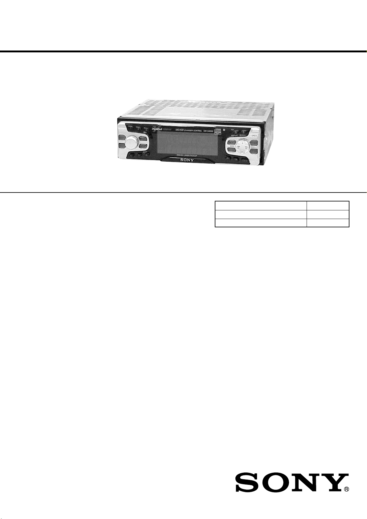
Photo: CDX-CA650X
• The tuner and CD sections have no adjustments.
SPECIFICATIONS
AEP Model
UK Model
Model Name Using Similar Mechanism NEW
CD Drive Mechanism Type MG-393X-121//Q
Optical Pick-up Name KSS-720A
CD player section
Signal-to-noise ratio 90 dB
Frequency response 10 – 20,000 Hz
Wow and flutter Below measurable limit
Tuner section
FM
Tuning range 87.5 – 108.0 MHz
Aerial terminal External aerial connector
Intermediate frequency 10.7 MHz/450 kHz
Usable sensitivity 8 dBf
Selectivity 75 dB at 400 kHz
Signal-to-noise ratio 66 dB (stereo),
72 dB (mono)
Harmonic distortion at 1 kHz
0.6% (stereo),
0.3% (mono)
Separation 35 dB at 1 kHz
Frequency response 30 – 15,000 Hz
MW/LW
Tuning range MW: 531 – 1,602 kHz
LW: 153 – 279 kHz
Aerial terminal External aerial connector
Intermediate frequency 10.7 MHz/450 kHz
Sensitivity MW: 30 µV
LW: 40 µV
Power amplifier section
Outputs Speaker outputs
(sure seal connectors)
Speaker impedance 4 – 8 ohms
Maximum power output 50 W × 4 (at 4 ohms)
General
Outputs Audio outputs
Power aerial relay control
lead
Power amplifier control lead
Inputs Telephone ATT control lead
Remote controller input
connector
Aerial input connector
Tone controls Bass ±8 dB at 100 Hz
Treble ±8 dB at 10 kHz
Power requirements 12 V DC car battery
(negative ground)
Dimensions Approx. 178 × 50 × 177 mm
(w/h/d)
Mounting dimension Approx. 182 × 53 × 161 mm
(w/h/d)
Mass Approx. 1.2 kg
Supplied accessories Parts for installation and
connections (1 set)
Front panel case (1)
Design and specifications are subject to change without
notice.
9-870-260-11
2001A0400-1
© 2001. 1
FM/MW/LW COMPACT DISC PLAYER
Sony Corporation
Audio Entertainment Group
General Engineering Dept.
1
Page 2
CDX-CA650/CA650V/CA650X
SERVICE NOTES
This label is located on the bottom of the chassis.
This label is located on the drive unit's internal
chassis.
When replacing the chassis (T.U) of mechanism deck which have
the “CAUTION LABEL” attached, please be sure to put a new
CAUTION LABEL (3-223-913-11) to the chassis (T.U).
NOTES ON HANDLING THE OPTICAL PICK-UP BLOCK
OR BASE UNIT
The laser diode in the optical pick-up block may suffer electrostatic
breakdown because of the potential difference generated by the
charged electrostatic load, etc. on clothing and the human body.
During repair, pay attention to electrostatic breakdown and also use
the procedure in the printed matter which is included in the repair
parts.
The flexible board is easily damaged and should be handled with
care.
NOTES ON LASER DIODE EMISSION CHECK
The laser beam on this model is concentrated so as to be focused on
the disc reflective surface by the objective lens in the optical pickup block. Therefore, when checking the laser diode emission, observe from more than 30 cm away from the objective lens.
Notes on Chip Component Replacement
• Never reuse a disconnected chip component.
• Notice that the minus side of a tantalum capacitor may be dam-
aged by heat.
TABLE OF CONTENTS
1. GENERAL
Location of Controls................................................................ 3
Getting Started ......................................................................... 3
CD Player ................................................................................ 4
Radio ....................................................................................... 5
RDS ......................................................................................... 6
Connections .............................................................................7
2. DISASSEMBLY
2-1. Sub Panel Assy.................................................................... 8
2-2. CD Mechanism Block ......................................................... 8
2-3. Main Board ......................................................................... 8
2-4. Heat Sink ............................................................................. 9
2-5. Chassis (T.U) Assy.............................................................. 9
2-6. Disc In Board, Guid (Disc) ...............................................10
2-7. Servo Board....................................................................... 10
2-8. Arm Roller Assy................................................................ 11
2-9. Chassis (OP) Assy............................................................. 11
2-10. Optical Pick-up Block ....................................................... 12
3. DIAGRAMS
3-1. IC Pin Descriptions ...........................................................13
3-2. Block Diagram –CD Section–........................................... 15
3-3. Block Diagram –Tuner Section–....................................... 16
3-4. Block Diagram –Display Section–.................................... 17
3-5. Circuit Boards Location .................................................... 17
3-6. Printed Wiring Boards –CD Mechanism Section–............ 18
3-7. Schematic Diagram –CD Mechanism Section–................ 20
3-8. Printed Wiring Board –Main Section– .............................. 21
3-9. Schematic Diagram –Main Section (1/2)–........................ 22
3-10. Schematic Diagram –Main Section (2/2)–........................ 23
3-11. Printed Wiring Board –Sub (CD) Section– ....................... 24
3-12. Schematic Diagram –Sub (CD) Section–.......................... 25
3-13. Schematic Diagram –Key Section– .................................. 26
3-14. Printed Wiring Board
–Key Section (CA650/CA650X)– ....................................27
3-15. Printed Wiring Board –Key Section (CA650V)–.............. 28
4. EXPLODED VIEWS
4-1. Chassis Section ................................................................. 32
4-2. Front Panel Section ...........................................................33
4-3. CD Mechanism Section (1) ............................................... 34
4-4. CD Mechanism Section (2) ............................................... 35
4-5. CD Mechanism Section (3) ............................................... 36
5. ELECTRICAL PARTS LIST ........................................ 37
SAFETY-RELATED COMPONENT WARNING!!
COMPONENTS IDENTIFIED BY MARK 0 OR DOTTED LINE
WITH MARK 0 ON THE SCHEMATIC DIAGRAMS AND IN
THE PARTS LIST ARE CRITICAL TO SAFE OPERATION.
REPLACE THESE COMPONENTS WITH SONY PAR TS WHOSE
P ART NUMBERS APPEAR AS SHO WN IN THIS MANUAL OR
IN SUPPLEMENTS PUBLISHED BY SONY.
2
Page 3
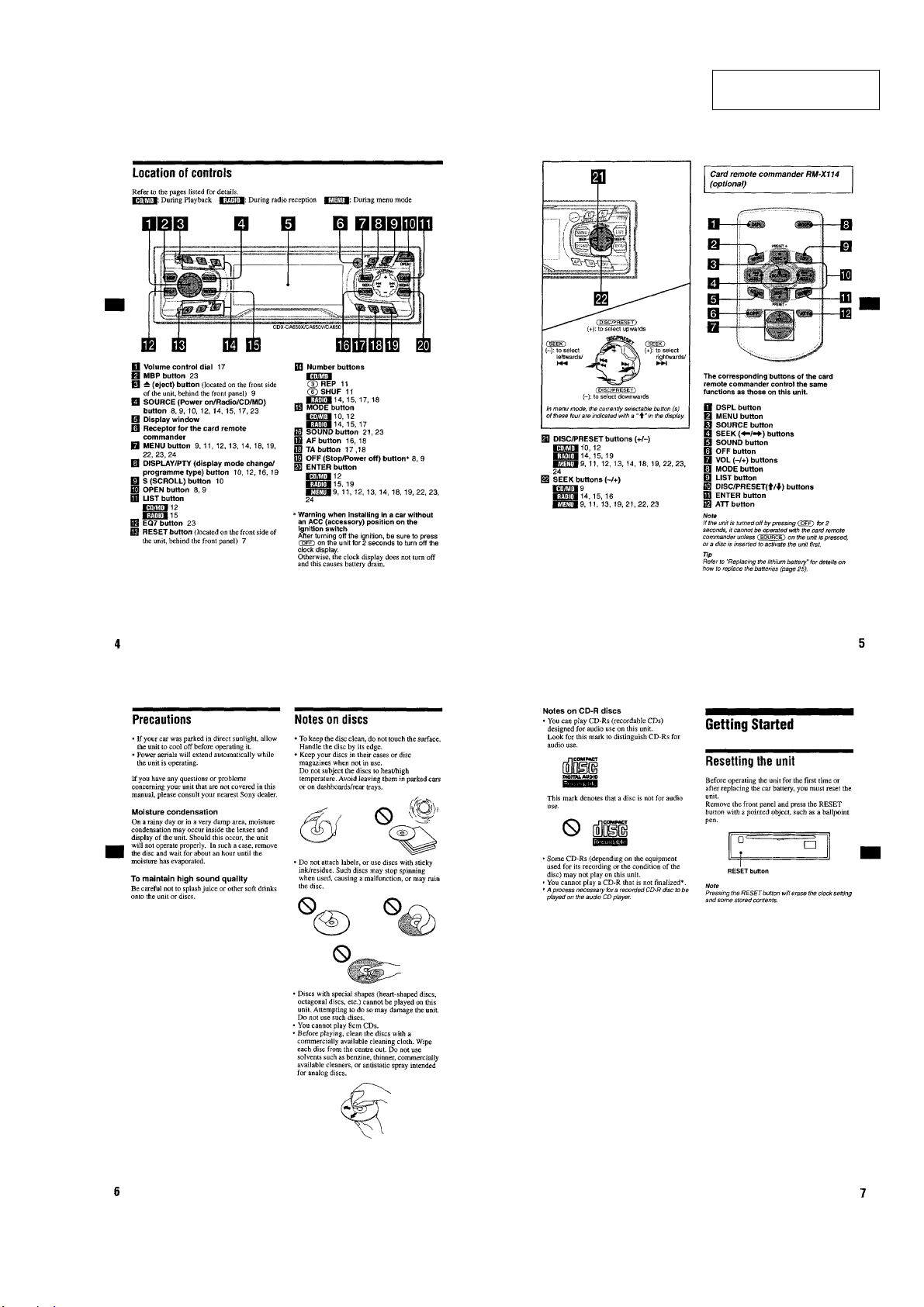
SECTION 1
GENERAL
CDX-CA650/CA650V/CA650X
This section is extracted
from instruction manual.
3
Page 4
CDX-CA650/CA650V/CA650X
4
Page 5
CDX-CA650/CA650V/CA650X
5
Page 6
CDX-CA650/CA650V/CA650X
6
Page 7
CDX-CA650/CA650V/CA650X
77
Page 8
CDX-CA650/CA650V/CA650X
4
4
SECTION 2
DISASSEMBLY
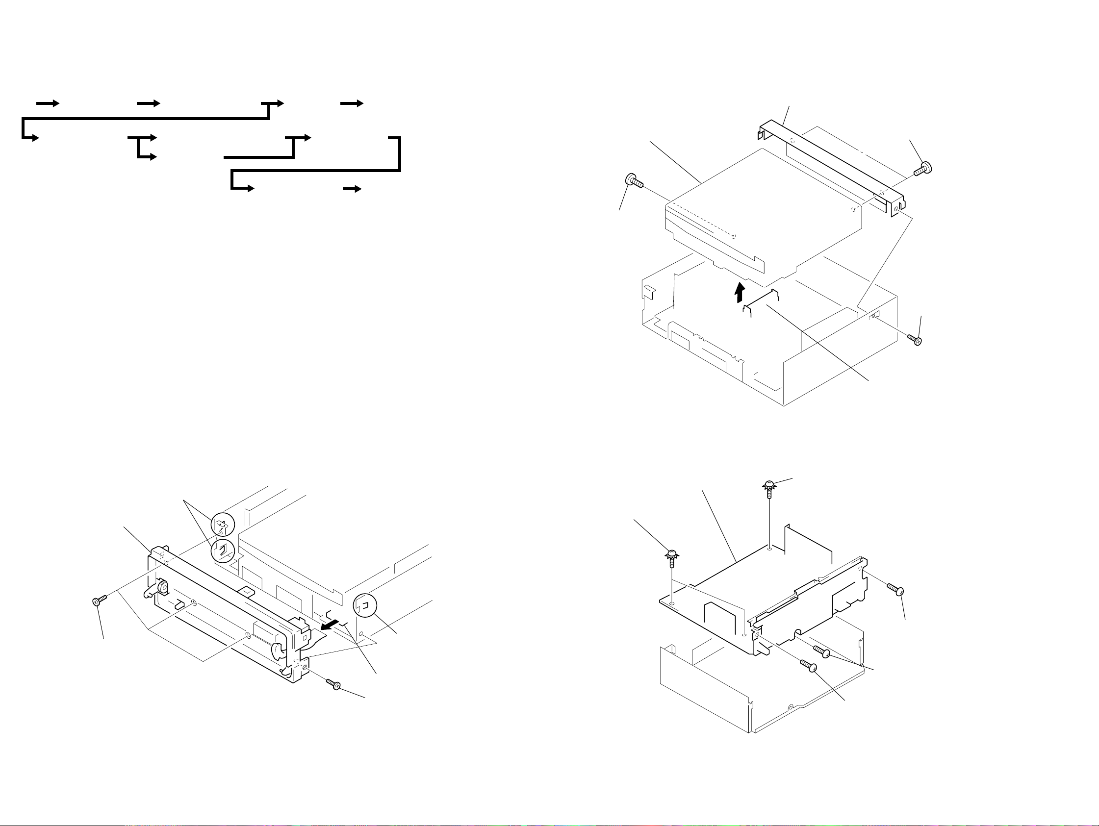
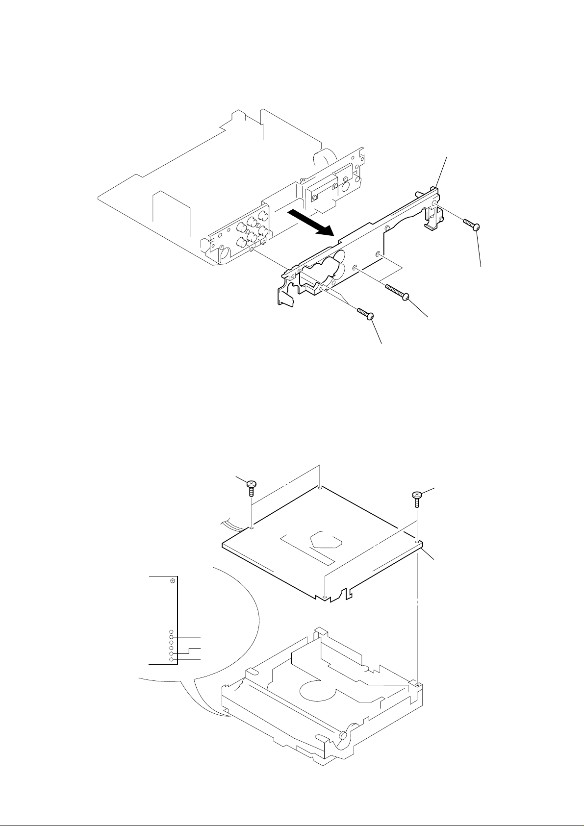
• The equipment can be removed using the following procedure.
Set Sub Panel Assy CD Mechanism Block
Chassis (T.U) Assy Disc In Board, Guide (Disc)
Servo Board
Main Board Heat Sink
Arm Roller Assy
Chassis (OP) Assy Optical Pick-up Block
2-2. CD MECHANISM BLOCK
5 CD mechanism block
2 PTT 2.6x4
7 bracket (CD)
6 PTT 2.6x4
3
1 PTT 2.6x
Note : Follow the disassembly procedure in the numerical order given.
2-1. SUB PANEL ASSY
4 two claws
6 sub panel assy
2 PTT 2.6x6
3 claw
2-3. MAIN BOARD
6 MAIN board
5 ground point screws
(PTT 2.6x6)
4 CNP301
4 ground point screw
(PTT 2.6x6)
3 PTT 2.6x
5 CN701
1 PTT 2.6x6
2 PTT 2.6x4
1 PTT 2.6x4
88
Page 9
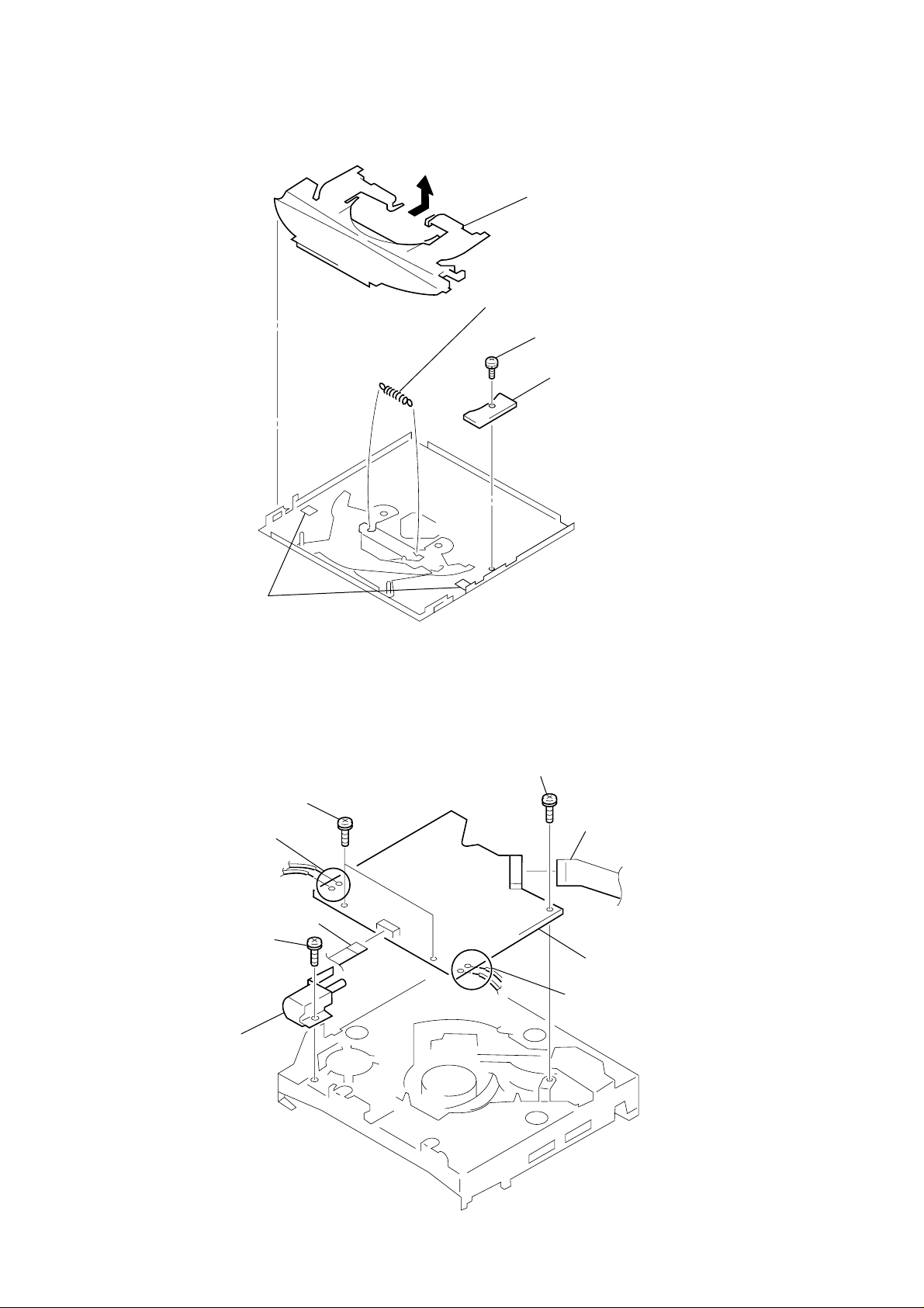
2-4. HEAT SINK
0
CDX-CA650/CA650V/CA650X
4 heat sink
3 PTT 2.6x1
2-5. CHASSIS (T.U) ASSY
1 Unsolder the
lead wires.
2 PTT 2.6x16
1 PTT 2.6x10
2 P 2x3
3 P 2x3
4 chassis (T.U) assy
black
red
white
9
Page 10
CDX-CA650/CA650V/CA650X
2-6. DISC IN BOARD, GUIDE (DISC)
4 guide (disc)
3 tension spring (LR)
1 PS 2x4
2 DISC IN board
2-7. SERVO BOARD
3 Removal the solders.
6 loading motor assy
(M903)
4 claws
7 PS 2x4
8 PS 2x4
2 CN2
1 CN3
5 P 2x3
9 SERVO board
4 Removal the solders.
10
Page 11
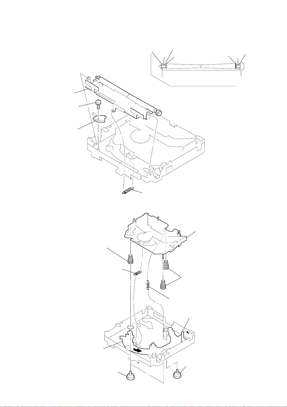
Fig. 1
3 PS 2x3
4 LOAD board
1 tension spring (RA3)
2 arm roller assy
retaining ring (roller)
arm
arm
washer(RA)
washer(RA)
bearing (roller)
bearing (roller)
2-8. ARM ROLLER ASSY
• When installing, take note of the positions
arm (roller) and washers. (Fig. 1)
CDX-CA650/CA650V/CA650X
2-9. CHASSIS (OP) ASSY
8 compression spring (FL)
1 tension spring (KF1)
6 Turn loading ring in the
direction of the arrow.
9 compression spring (FL)
2 tension spring (KR1)
7 chassis (OP) assy
5 Fit lever (D) in the
direction of the arrow.
4 damper (T)
3 damper (T)
11
Page 12
CDX-CA650/CA650V/CA650X
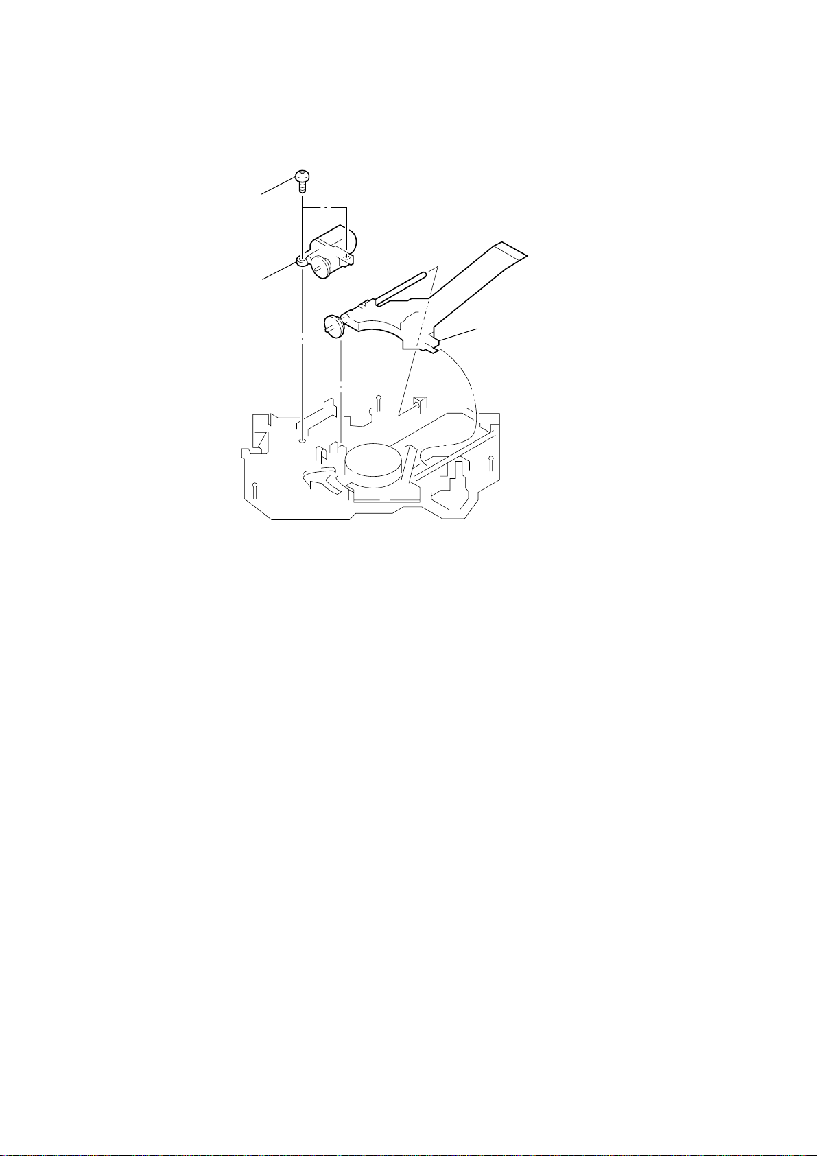
2-10. OPTICAL PICK-UP BLOCK
1 P 2x3
2 sled motor assy
(M902)
3 optical pick-up block
12
Page 13
CDX-CA650/CA650V/CA650X
SECTION 3
DIAGRAMS
3-1. IC PIN DESCRIPTION
• IC501 MN101C49KTH (SYSTEM CONTROL)
Pin No. Pin Name I/O Pin Description
1 VREF– — A/D converter power supply (–) pin
2 VSM I S-meter voltage detection input
3 NIL (FMAGC) I Not used. (Connect to VSS in this set)
4, 5 KEYIN1, 0 I Key input 1, 0
6 RCIN0 I Rotary commander key input
7 QUALITY I Noise detection input
8 MPTH I Multipath detection input
9 NIL (DSTSEL) I Not used. (Fixed at L in this set)
10 VREF+ — A/D converter power supply (+) pin (+5 V)
11 VDD — Power supply pin (+5 V)
12 OSCOUT O Main clock output (18.43 MHz)
13 OSCIN I Main clock input (18.43 MHz)
14 VSS — Ground
15 XIN I Sub clock input (32.768 kHz)
16 XOUT O Sub clock output (32.768 kHz)
17 MMOD I Memory mode select input (Fixed at L in this set)
18 LCDSO O Serial data output for LCD driver IC.
19 LCDCE O Chip enable output for LCD driver IC.
20 LCDCKO O Serial clock output for LCD driver IC.
21 CD TSO O Serial data output for CD servo IC.
22 CD TSI I Serial data input from CD servo IC.
23 CD TCKO O Serial clock output for CD servo IC.
24 SYSRST O System reset output
25 BUSON O BUS ON output
26 KEYACK I Key acknowledge detection input
27 DAVN I RDS data block synchronization detection input
28 BUIN I Backup power supply input
29 SIRCS I SIRCS input
30 CD SELFSW I CD mechanism deck Self switch detection input
31 CD PACK I CD text pack synchronization signal input from CD servo IC.
32 VDD2 — Power supply pin (+5 V)
33 RESET I Microcomputer reset input
34 NOSESW I Front panel attachment detection input
35 BEEP O Beep output
36 NCO O Not used. (Open)
37 TESTIN I Test mode detection input
38 ACCIN I Accessory power supply detection input
39 NCO (VCC) O Not used. (Open)
40 TELATT I Telephone attenuator detection input
41 NCO (VCC) I Not used. (Fixed at H in this set)
42 UNISO O SONY-BUS data output
43 UNISI I SONY-BUS data input
44 UNICKO O SONY-BUS clock output
45 12C SIO I/O I2C BUS serial data input/output
46 NCO O Not used. (Open)
47 12C CKO O I2C BUS serial clock output
48 NCO O Not used. (Open)
49 TUNON O Tuner power supply control output
50 PW ON O System power supply control output
51 TSTB O CD text parameter strobe output for CD servo IC.
52 RFOK I RFOK signal input from CD servo IC.
13
Page 14
CDX-CA650/CA650V/CA650X
Pin No. Pin Name I/O Pin Description
53 CD RST O Reset signal output for CD servo IC.
54 A0 O Command/parameter discrimination signal output for CD servo IC.
55 STB O Data strobe signal output for CD servo IC.
56 X EN O Crystal oscillation control output for CD servo IC.
57 LIMIT I CD mechanism deck Limit switch detection input
58 PH1 I CD mechanism deck PH1 detection input (Not used in this set)
59 D SW I CD mechanism deck Down switch detection input
60 INSW I CD mechanism deck Disc in switch detection input
61 NC (PH3) O CD mechanism deck PH3 detection input (Not used in this set)
62 CD LM LO O CD mechanism deck loading motor control output (Loading direction)
63 CD LM EJ O CD mechanism deck loading motor control output (Eject direction)
64, 65 NCO O Not used. (Open)
66 AMPATT O Power amplifier attenuator control output
67 AMPON O Power amplifier standby control output
68 CDMD ON O CD mechanism deck power supply control output
69 ATT O System attenuator control output
70 VOLATT O Electric volume attenuator control output
71 – 75 NCO O Not used. (Open)
76 COLSW I
77 COLSEL I 1 color initial setting input (L: amber, H: green) (Fixed at L in this set)
78 DIMSEL I
79 XCD ON O CD signal processing crystal drive output
80 NCO O Not used. (Fixed at L in this set)
81 – 85 NCO O Not used. (Open)
86 E2P SIO I/O EEPROM serial data input/output
87 E2P CKO O EEPROM serial clock output
88 NCO O Not used. (Open)
89 FLASH W I Flash microcomputer write detection input
90 NS MASK O Noise mask output
91 AD ON O Key power supply control output
92 DOORIND O Sub panel power control output
93 ILLON O Illumination power control output
94 DOORSW I Front panel OPEN/CLOSE detection input
95 DA VSS — D/A converter power supply (–) pin
96, 97 REIN1, 0 I Rotary encoder input 1, 0
98 RCIN1 I Rotary commander SHIFT key input
99 RAMBU I Not used. (Fixed at L in this set)
100 DAVDD — D/A converter power supply (+) pin (+5 V)
Key illumination 1 color/2 color select initial setting input
(L: 1 COLOR, H: 2 COLOR) (Fixed at L: CDX-CA650, H: CDX-CA650V/CA650X)
Manual dimmer initial setting input (L: dimmer without, H: dimmer with)
(Fixed at L: CDX-CA650/CA650X, H: CDX-CA650V)
14
Page 15

3-2. BLOCK DIAGRAM — CD SECTION —
OPTICAL PICK-UP
KSS-720A
RF AMP,DIGITAL SERVO
DIGITAL SIGNAL PROCESSOR
IC1
CDX-CA650/CA650V/CA650X
A
C
B
D
E
F
PD
LD
FOCUS
COIL
TRACKING
COIL
I-V
CONV.
M902
(SLED)
LD
DRIVE
Q1
A
82
C
83
B
84
D
85
E
87
F
86
PD
97
LD
98
FOCUS/TRACKING COIL DRIVE
SLED/SPINDLE/LOADING MOTOR DRIVE
15
16
17
18
M
13
14
FOCUS
DRIVE
TRACKING
DRIVE
MOTOR
DRIVE
TRACKING
LD AMP
IC2
COIL
COIL
SLED
ERROR
(Page 16)
TUNER
LOUT
RF
EQ
FORCUS
ERROR
FD
26
TD
23
SD
5
EFM
DEMOD
SERVO
CTL
FDTDSD
62 63 64 65
MD
D/A
CONV
DSUB CODE
PROCESS
I/F
OSC
23 24
X1
16.9344MHz
ROUT
PACK
TSTB
SCK
STB
RST
RFOK
XTALEN
16
12
R-CH
52
56
SI
8
SO
7
6
5
AO
4
3
2
9
SW1
(DISC IN)
SW2
(SELF)
SW3
(LIMIT)
SW4
(DOWN)
CDL
SECTION
A
SYSTEM CONTROL
CD PACK
31
TSTB
51
21
CD TSO
22
CD TSI
23
CD TCKO
55
STB
54
AO
53
CD RST
52
RFOK
XEN
56
60
IN SW
30
CD SELF SW
LIMIT
57
59
D SW
IC501(1/3)
28
BU IN
24 13 2
SYS RST
25
BUS ON
42
UNI SO
43 8
UNI SI
44
UNI CKO
33
RESET
10 3
12 1
9
11 4
BUS INTERFACE
IC505
IC602
1
RESET
BATT DET
Q556
8
6
6
2
5
4
CNJ600
(BUS CONTROL IN)
BU 5V
7
BATT
3
2
1
M901
(SPINDLE)
M903
(LOADING)
M
11
12
M
9
10
SPINDLE
MOTOR
DRIVE
LOADING
MOTOR
DRIVE
MD
6
LOAD
1
EJECT
2
POWER
CONTROL
BATT
Q332
POWER
CONTROL
Q333
A5V
AU5V
D5V
DR6V
REG
Q341
REG
Q331
62
63
68
79
CD LM LO
CD LM EJ
CDMD ON
XCD ON
S702
RESET
• Signal path
:CD
15 15
Page 16

CDX-CA650/CA650V/CA650X
3-3. BLOCK DIAGRAM — TUNER SECTION —
J10
(ANTENNA)
TUNER UNIT
TU10
ANTFM MPX
2 10
AM DET
ANTAM
1
S-METER
I2C SDA
I2C SCL
RDS DET
PJ401-1,-2
BUS AUDIO IN
-1
-2
L
R
(Page 15)
A
CD
SECTION
8
BUFFER
Q10
IC20
NOISE
5 1
SUPPRESSOR
Q22
NOISE
SUPPRESSOR
ON
14
12
13
9
10
SDA SCL
MULTI
LV IN
20 2
9
16
MPX
PATH
DET
RDS/RDBS
DEM/DEC
CDL
RDS DECODER
IC51
8
ELECTRONIC VOLUME
R-CH
AUX LCH OUT FL
4 28
MD LCH
43
MPXI
12
AM
9
LEVEL
13
MPIN
14
SDA
19
SCL
20
EXA ATT
17
SYSTEM CONTROL
VOL ATT
70
QUALITY
7
NS MASK
90
VSM
2
I2C SIO
45
I2C CKO
47
MPTH
8
DAVN
27
IC401
IC501 (2/3)
AMP ATT
OUT RL
ATT
BEEP
AMP ON
TEL ATT
ACC IN
TEST IN
TUN ON
PW ON
27
Q451
MUTE
Q478,479
69
35
67
66
40
38
37
49
50
MUTE
CONT
PJ401-3, -4
AUDIO OUT REAR
-3L-4
R
R-CH
Q431
MUTE
BATT
PJ401-5, -6
AUDIO OUT FRONT
-5L-6
R
R-CH
ACC
CHECK
Q631
POWER SUPPLY
IC601
7 6
VCC AMP +B
2
3
4
8.7V ON
5.6V ON
STB
ANT +B
BU+B BU 5V
COM 8V
TU 5.6V
TU 8.7V
POWER AMP
12
11
AUX
16
STBY
4
MUTE
22
TEL
ATT
Q651
8
5
9
10
11
IC404
BATT
COM 8V
TU 5.6V
TU 8.7V
CNP601
1
5
3
9
7
R-CH
F901
FL+
9
FL–
2
RL+
10
RL–
4
FR+
12
FR–
3
RR+
11
RR–
16
BATT
13
ATT
7
ACC
15
TEST
5
AMP R
6
ANT R
E2PROM SDA
E2PROM SCL
OSCO OSCI
4 5
X51
4.332MHz
• Signal path
:FM
:MW
17
18
86
87
E2P SIO
E2P CKO
:CD
1616
Page 17

3-4. BLOCK DIAGRAM — DISPLAY SECTION — 3-5. CIRCUIT BOARDS LOCATION
t
CDX-CA650/CA650V/CA650X
KEY MATRIX
LSW901-911,914-919
S902-907
LSW801
J501
(REMOTE IN)
S701
(NOSE DET)
KEY
ACTIVE
Q665
IC971
IR
RECEIVE
ROTARY
ENCODER
RE901
X502
32.768kHz
SYSTEM CONTROL
IC501 (3/3)
KEY IN0
5
KEY IN1
KEY ACK
26
AD ON
91
RC IN1
98
RC IN0
6
SIRCS
29
RE IN0
97
RE IN1
96
NOSE SW
34
XIN
15
XOUT
16
LCD SO
LCD CKO
LCD CE
DOOR IND
ILL ON
OSC OUT
OSC IN
LCD DRIVE
IC900
18
20
194
92
78
77
76
DOOR IND
DRIVE
Q633
DATA
CLK
CE
GREEN
AMBER
LCD901
SUB (CD) board
80
79
CA650
AMBER
DRIVE
Q901
GREEN
DRIVE
Q902
LED
DRIVE
Q906
LED
DRIVE
Q905
CA650V
DISC IN board
SUB board
LIMIT board
tuner uni
(TU10)
LED801,LSW801
POWER
93
12
13
CONT
Q662
BATT
X501
18.43MHz
REG
Q660,661
LSW901-911,814-919
LED900,901,913,914
ILL +B
LED902,903
LED905,906
909,910
LOAD board
KEY board
MAIN board
SERVO board
• Waveforms
— Servo Board —
(MODE: CD PLAY)
— Main Board —
1
2
3
4
5
16.9344MHz
IC1
IC1
(X TAL)
wd
3.4msec
(PACK)
ts
IC1
IC1
(RFO)
uj
Approx. 620mVp-p
(FEO)
oa
2.4Vp-p
4.8Vp-p
1.8Vp-p
0V
1
2
3
IC51
IC501
IC501
4.332MHz
(OSCI)
5
18.43MHz
(
OSCIN
qd
32.768kHz
(XIN)
qg
3.6Vp-p
1.8Vp-p
)
2.2Vp-p
Approx. 200mVp-p
od
(TEO)
IC1
0V
17 17
Page 18

CDX-CA650/CA650V/CA650X
THIS NOTE IS COMMON FOR PRINTED WIRING
BOARDS AND SCHEMATIC DIAGRAMS.
(In addition to this, the necessary note is
printed in each block.)
for schematic diagram:
• All capacitors are in µF unless otherwise noted. pF: µµF
50 WV or less are not indicated except for electrolytics
and tantalums.
• All resistors are in Ω and 1/
specified.
• % : indicates tolerance.
f
•
• C : panel designation.
Note: The components identified by mark 0 or dotted line
• A : B+ Line.
• Power voltage is dc 14.4V and fed with regulated dc power
• V oltages are taken with a VOM (Input impedance 10 MΩ).
• Waveforms are taken with a oscilloscope.
• Circled numbers refer to waveforms.
• Signal path.
: internal component.
with mark 0 are critical for safety.
Replace only with part number specified.
supply from ACC and BATT cords.
Voltage variations may be noted due to normal produc-
tion tolerances.
Voltage variations may be noted due to normal production tolerances.
F : FM
f : MW
J : CD
4
W or less unless otherwise
3-6. PRINTED WIRING BOARDS — CD MECHANISM SECTION —
for printed wiring boards:
• X : parts extracted from the component side.
• Y : parts extracted from the conductor side.
• x : parts mounted on the conductor side.
a
•
• : Pattern from the side which enables seeing.
Caution:
Pattern face side: Parts on the pattern face side seen from the
(Side B) pattern face are indicated.
Parts face side: Parts on the parts face side seen from the
(Side A) parts face are indicated.
: Through hole.
(The other layer’s patterns are not indicated.)
1818
Page 19

(Page 21)
CDX-CA650/CA650V/CA650X
• Semiconductor
Location
Ref. No. Location
IC1 D-2
IC2 G-2
Q1 B-3
19 19
Page 20

CDX-CA650/CA650V/CA650X
• Refer to page 17 for Waveforms.
3-7. SCHEMATIC DIAGRAM — CD MECHANISM SECTION — • Refer to page 29 for IC Block Diagrams.
IC B/D
(Page 22)
IC B/D
Note:
• Voltage is dc with respect to
ground under no-signal conditions.
no mark : CD PLAY
2020
Page 21

3-8. PRINTED WIRING BOARD — MAIN SECTION —
CDX-CA650/CA650V/CA650X
(Page 19)
• Semiconductor Location
Ref. No. Location
D21 J-2
D22 J-2
D23 I-3
D331 H-13
D332 H-13
D341 G-9
D471 A-9
D472 A-9
D473 A-9
D474 A-9
D475 C-8
D476 A-10
D477 C-8
D478 A-11
D479 D-8
D551 D-13
D553 B-12
D554 C-12
D555 C-12
D556 D-13
D601 B-12
D609 E-11
D610 E-6
D611 B-11
D612 D-10
D613 D-10
D614 C-11
D621 G-13
D662 J-13
D671 K-4
D701 J-4
D710 L-3
D711 K-2
Ref. No. Location
D713 L-2
D714 L-2
D720 K-2
IC20 I-1
IC51 I-4
IC401 D-4
IC404 B-7
IC501 I-8
IC505 I-11
IC601 F-13
IC602 J-10
Q21 J-2
Q22 I-3
Q331 H-13
Q332 I-13
Q333 H-13
Q341 G-10
Q431 B-5
Q441 B-5
Q451 B-4
Q461 B-4
Q478 E-8
Q479 E-9
Q556 C-13
Q631 E-10
Q651 E-10
Q660 I-14
Q661 J-13
Q662 I-13
Q663 J-14
Q664 J-6
(Page 24)
21 21
Page 22

CDX-CA650/CA650V/CA650X
• Refer to page 17 for Waveforms.
3-9. SCHEMATIC DIAGRAM — MAIN SECTION (1/2) — • Refer to page 29 for IC Block Diagrams.
IC B/D
(Page 20)
IC B/D
(Page 23)
Note:
• Voltage is dc with respect to ground under
no-signal (detuned) condition.
no mark : FM
( ) : MW
< > : CD PLAY
2222
Page 23

3-10. SCHEMATIC DIAGRAM — MAIN SECTION (2/2) — • Refer to page 29 for IC Block Diagrams.
CDX-CA650/CA650V/CA650X
(Page 22)
IC B/D
IC B/D
(Page 25)
23 23
Note:
• Voltage is dc with respect to ground under no-signal
(detuned) condition.
no mark : FM
Page 24

CDX-CA650/CA650V/CA650X
3-11. PRINTED WIRING BOARD — SUB (CD) SECTION —
(Page 21)
(Page 27, 28)
2424
Page 25

3-12. SCHEMATIC DIAGRAM — SUB (CD) SECTION —
CDX-CA650/CA650V/CA650X
(Page 23)
(Page 26)
25 25
Page 26

CDX-CA650/CA650V/CA650X
3-13. SCHEMATIC DIAGRAM — KEY SECTION —
(Page 25)
Note:
• Voltage is dc with respect to ground under no-signal
(detuned) condition.
no mark : FM
2626
Page 27

3-14. PRINTED WIRING BOARD — KEY SECTION (CA650/CA650X) —
CDX-CA650/CA650V/CA650X
• Semiconductor Location
Ref. No. Location
(D901) C-10
(D902) C-11
(D903) C-11
(D904) C-11
(D906) C-11
(D908) C-10
D971 A-11
(IC900) C-8
IC971 A-11
LED900 A-2
( ) : SIDE B
Ref. No. Location
LED901 C-2
LED902 B-1
LED903 B-1
LED905 A-4
LED906 A-10
LED909 B-10
LED910 B-4
LED913 B-12
LED914 B-13
(Q901) B-4
(Q902) C-4
(Page 24)
27 27
Page 28

CDX-CA650/CA650V/CA650X
3-15. PRINTED WIRING BOARD — KEY SECTION (CA650V) —
• Semiconductor Location
Ref. No. Location
(D901) B-10
(D902) C-11
(D903) C-11
(D904) C-11
(D906) C-11
(D908) C-10
D971 A-11
(IC900) B-8
IC971 A-10
( ) : SIDE B
Ref. No. Location
LED900 A-2
LED901 C-2
LED902 B-1
LED903 B-1
LED905 A-4
LED906 A-10
LED913 B-12
LED914 B-13
(Q905) B-5
(Q906) B-5
(Page 24)
2828
Page 29

• IC Block Diagrams
IC1 µPD63711GC-8EB
CDX-CA650/CA650V/CA650X
AGCI
RFO
EQ2
EQ1
AGND
AVDD
REFOUT
FEO
TEO
TE2
TEC
AGND
AVDD
RF-
FE-
TE-
AGCO74RFI73C3T72ASY71EFM70AVDD697E DAC3687D DAC2677C DAC1667F DAC065MD64SD63TD62FD
75
76
77
78
79
80
81
A
82
C
83
B
84
D
85
F
86
E
87
88
89
90
91
92
93
94
95
96
PD
97
LD
98
99
PN
100
EFM
COMPARATOR
EFM
FEOFS
TEOFS
RF
AMP BLOCK
EFM
SWITCH
DEFECT
FOK
A3T
MIRR
FEO
TEO
COMPARATOR
MICROCOMPUTER INTERFACE
AUTO GAIN
CONTROLLER
SVDRAM
PROCESSOR
DEFECT
COMPARATOR
RFENV
MIRENV
TRACKING
A/D CONVERTER
REGISTER
FOCUS
REGISTER
ADDER
MULTIPLIER
SVROM
CLV
D/A
FD/TD/SD/MD
CONTROLLER
SVCRAM
ROM
DECODER
ATEST59TEST158TEST057DGND56TSTB55TSCK54TSI53TSO52PACK51DVDD
AGND
60
61
MICROCOMPUTER INTERFACE
CD-TEXT DECODER
D/A
INTERFACE
CIRCUIT
OCTUPLED
NOISE SHAVER
OUTPUT BUFFER
SUB-CODE PROCESSOR
OSC
MEMORY
PROCESSOR
SCF
16K
SRAM
EFM DEMODULATOR
TIMING GENERATOR
DE-EMPHASIS CIRCUIT
OVERSAMPLING DIGITAL FILTER
NOISE SHAVER
OUTPUT BUFFER
DIGITAL PLL
DIGITAL
AUDIO
INTERFACE
OUTPUT PROCESSOR
ERROR
PROCESSOR
CORRECTION
C2D3
50
C2D2
49
C2D1
48
C1D2
47
C1D1
46
DGND
45
PLCK
44
MIRR/WFCK
43
RFCK
42
LOCK
41
DVDD
40
TSOI
39
C16M
38
DGND
37
TX
36
HOLD/WDCK
35
LRCK
34
LRCKIN
33
SCKO
32
SCKIN
31
DOUT
30
DIN
29
FLAG
28
EMPH
27
DVDD
26
1
2
3
RST
RFOK
DGND
IC51 SAA6588T
CIN
LVIN
20
19
MULTI
PATH
DETECTOR
CLOCKED
COMPARATOR
RDS/RDBS
DEMODULATOR
OSCILLATOR
TEST
CONTROL
2
1
3
MRO
TCON
MPTH
4A05
SCOUT
18
BAND-PASS FILTER
RDS/RDBS
DECODER
& CLOCK
4 5
OSCI
OSCO
6
STB
SCK
57kHz
8th ORDER
6
7SO8SI9
CLOCK
DATA
7
VSSD
VDDD
XTALEN
VREF
17
SIGNAL QUALITY
DECODER
445
INTERFACE
REGISTER
8
DAVN
10
DVDD
VSSA
MPX
15
POWER SUPPLY
& RESET
11
DAVDD
12
ROUT
VDDA
14
CLOCK
DATA
IIC BUS SLAVE
TRANSCEIVER
9 10
13
DAGND
1316
SDA
AFIN
DETECTOR
SCL
1514
REGC
PAUSE
16
DAGND
17
18R+19R–20L+21L–22
LOUT
DAVDD
MAD
PSWN
11
12
23
XTAL24XTAL
XVDD
25
XGND
29
Page 30

CDX-CA650/CA650V/CA650X
1
2
3
4
5
6
7 8
9
10
14
13
12
11
BUS ON
SWITCH
RESET
SWITCH
BATTERY
SWITCH
BUS ON
RST
BATT
CLK
VREF
DATA
GND
VCC
RST
BUS ON
CLK IN
BU IN
DATA IN
DATA OUT
IC2 BA5810FP
FWD
1
REV
2
LDCONT
3
PS
4
IN1
5
IN2
6
PREVCC
7
POWVCC
8
VOL–
9
VOL+
10
VO2–
11
VO2+
12
VO1–
13
VO1+
14
X3
PREVCC
(PRE.LOADING)
POWVCC12
(CH1.CH2)
10k
–
+
+
–
10k
10k
–
+
+
–
10k
POWER
SAVE
10k
10k
10k
10k
LOADING PRE
7.5k
–
16k
LEVEL
SHIFT
FWD REV
7.5k
16k
+
LEVEL
SHIFT
IC505 BA8270F
BIAS
28
+
–
+
7.5k
–
+
–
+
–
16k
7.5k
+
LEVEL
SHIFT
MUTE
16k
POWVCC34
(CH3,CH4)
10k
–
+
+
–
CH1-4
–
10k
10k
–
LEVEL
SHIFT
+
+
–
10k
10k
10k
10k
10k
27
26
25
24
23
22
21
20
19
18
17
16
15
OPIN4+
OPIN4–
OPOUT4
OPIN3+
OPIN3–
OPOUT3
MUTE
POWVCC
GND
VO3–
VO3+
VO4–
VO4+
30
IC601 BA4908-V3
2 3
1
NC
MODE2
4
STB
MODE1
REGULATOR
OVER VOLTAGE
PROTECT
–
+
5 6 7 8 9
ANT
VCC
VDD
AMP
COM
–
+
10
AM
–
+
11
FM
–
+
12
GND
Page 31

IC401 TDA7406T
CDX-CA650/CA650V/CA650X
SWIN
ACINR
ACOUTR
SWACOUT
AC OUTL
CREF
MIXINFL
MIXINRL
MIXINFR
MIXINRR
OUTFL
OUTRL
28 2730 2932 31
MIXER
SOFT STEP
FADER
OUTPUT SELECTOR
HIGH PASS
7BAND
EQUALIZER
SOFT STEP
VOLUME
SOFT MUTE
LOUDNESS
IN GAIN
+ AUTO
ZERO
OUTFR
OUTRR
26 25 24 23
SOFT STEP
FADER
OUTSW
SOFT STEP
FADER
SUB
WOOFER
FILTER
MONO
FADER
IIC-BUS
HIGH OUT
S & H
25kHz
LP
DEMODULATOR
+STEREO ADJUST
+STEREO BLEND
PILOT
CANCELLATION
SPECTRUM
ANALIZER
BEEP
PAUSE
DIGITAL
CONTROL
SAOUT
QUAL.
PIL, DET
PLL
CREF
DETECTOR
MULTI
PATH
SUPPLY
PULSE
FORMER
AM/FM
NOISE
BLANKER
A/D
22
21
20
19
18
17
16
15
14
13
VDD
SACLK
SCL
SDA
GND
ATT
QUAL
MP OUT
MP IN
LEVEL
ACINL
33
34
35
36
37
38
39
CDR
CDL
MDR
MDL
TAPEL
MAIN SOURCE
40
41
42
43
44
SELECTOR
INPUT MULTIPLEXER
1 2 3 4 5 6 7 8 9 10 11
FDL–
FDR+
TAPE R
FDL+
PAUSE
MIXING
SELECTOR
TIM
PHONE
NAVI
86kHz
LP
STD
IN GAIN
AM/MPX2
AMIF
CMPX
12
AUX1
31
Page 32

CDX-CA650/CA650V/CA650X
NOTE:
• The mechanical parts with no reference
number in the exploded views are not supplied.
• Items marked “*” are not stocked since
they are seldom required for routine service.
Some delay should be anticipated
when ordering these items.
• -XX and -X mean standardized parts, so
they may have some difference from the
original one.
SECTION 4
EXPLODED VIEWS
• Color Indication of Appearance Parts
Example :
KNOB, BALANCE (WHITE) ... (RED)
R
Parts Color Cabinet’s Color
• Accessories and packing materials and
hardware (# mark) list are given in
the last of this parts list.
The components identified by
mark 0 or dotted line with mark.
R
0 are critical for safety.
Replace only with part number
specified.
4-1. CHASSIS SECTION
8
2
1
11
10
9
MG-393X-121//Q
#1
#1
#1
14
#5
#6
#6
17
12
#4
#7
#6
16
15
TU10
4
3
7
5
6
#1
#4
17
18
19
#1
#5
#5
#6
13
#1
F901
#2
#3
#2
#3
#3
22
Ref. No. Part No. Description Remark
1 X-3378-512-1 PANEL ASSY, SUB
2 3-040-990-01 BUTTON (EJECT)
* 3 1-680-762-11 SUB (CD) BOARD
4 X-3376-699-1 GEAR ASSY
5 3-030-909-01 DAMPER, OIL
6 3-713-786-51 SCREW +P 2X3
7 X-3377-621-1 LOCK ASSY
* 8 3-223-782-01 COVER
9 1-776-527-61 CORD (WITH CONNECTOR) (ISO) (POWER)
* 10 3-041-012-01 BRACKET (CD)
* 11 3-227-287-01 SHEET, DUST PROTECTION
* 12 3-223-783-01 CHASSIS (BACK)
* 13 3-223-780-11 HEAT SINK
#1
20
#1
21
Ref. No. Part No. Description Remark
* 14 A-3326-846-A MAIN BOARD, COMPLETE (CA650)
* 14 A-3326-849-A MAIN BOARD, COMPLETE (CA650X)
* 14 A-3326-852-A MAIN BOARD, COMPLETE (CA650V)
* 15 3-040-998-01 BRACKET (IC)
* 16 3-041-011-01 HEAT SINK (REG)
17 3-376-464-11 SCREW (+PTT 2.6X6), GROUND POINT
* 18 3-045-878-01 PLATE (TU), GROUND
* 19 3-045-877-01 CUSHION (TU)
* 20 3-224-755-01 SHEET, INSULATING
* 21 3-223-781-01 CHASSIS
22 3-047-812-01 SCREW (LOCK)
F901 1-532-877-11 FUSE (BLADE TYPE) (AUTO FUSE) 10A
TU10 A-3220-812-A TUNER UNIT (TUX-020)
32
Page 33

8
4-2. FRONT PANEL SECTION
67
CDX-CA650/CA650V/CA650X
#8
#8
57
#
63
LCD901
58
65
62
64
66
56
61
not supplied
(KEY board)
67
60
51
52
59
53
54
55
51 3-223-789-01 BUTTON (DSPL/SCRL)
52 3-223-791-01 BUTTON (MENU/SOUND)
53 3-223-792-01 BUTTON (AF/TA/OFF)
54 3-223-790-01 BUTTON (LIST/ENTER)
55 X-3380-529-1 SUB ASSY, PANEL (CA650X)
55 X-3380-530-1 SUB ASSY, PANEL (CA650)
55 X-3380-531-1 SUB ASSY, PANEL (CA650V)
* 56 3-223-798-01 HOLDER (LCD)
57 X-3380-079-1 PANEL ASSY, FRONT BACK
58 X-3380-080-1 KNOB (VOL) ASSY (CA650V/CA650X)
58 X-3380-081-1 KNOB (VOL) ASSY (CA650)
59 3-223-751-01 BUTTON (4-6)
Ref. No. Part No. Description RemarkRef. No. Part No. Description Remark
60 3-223-753-01 BUTTON (SOURCE/MODE)
61 3-223-750-01 BUTTON (1-3)
62 3-223-752-11 BUTTON (DSO/EQ7)
* 63 3-223-799-01 PLATE (LCD), GROUND
64 1-694-780-11 CONDUCTIVE BOARD, CONNECTION
* 65 3-223-800-01 ILLUMINATOR (LCD) (CA650/CA650X)
* 65 3-231-293-01 ILLUMINATOR (LCD) (CA650V)
* 66 3-223-797-01 PLATE (LCD), LIGHT GUIDE
* 67 3-231-648-01 SHEET (LIGHT INTERCEPTION) (CA650V)
LCD901 1-804-292-11 DISPLAY PANEL, LIQUID CRYSTAL (CA650)
LCD901 1-804-292-31 DISPLAY PANEL, LIQUID CRYSTAL (CA650X)
LCD901 1-804-293-11 DISPLAY PANEL, LIQUID CRYSTAL (CA650V)
33
Page 34

CDX-CA650/CA650V/CA650X
4-3. CD MECHANISM SECTION (1)
(MG-393X-121//Q)
103
#11
104
105
#9
102
101
#9
C
108
C
107
109
#11
#11
Ref. No. Part No. Description Remark Ref. No. Part No. Description Remark
101 A-3315-247-A CHASSIS (T.U) ASSY
102 3-931-909-01 SPRING (LR), TENSION
* 103 1-659-836-11 DISC IN BOARD
104 3-338-737-01 SCREW (2X3), +PS
* 105 1-659-837-11 LOAD BOARD
* 106 3-039-629-01 BRACKET (MOTOR)
* 107 A-3283-047-A SERVO BOARD, COMPLETE
108 3-225-784-01 SPRING (RA3), TENSION
109 A-3315-040-A ROLLER ASSY, ARM
M903 A-3315-039-A MOTOR SUB ASSY, LD (LOADING)
M903
#10
106
#9
34
Page 35

4-4. CD MECHANISM SECTION (2)
(MG-393X-121//Q)
CDX-CA650/CA650V/CA650X
155
157
158
162
163
154
D
160
155
165
151
156
157
166
167
153
164
161
D
159
152
152
152
Ref. No. Part No. Description Remark Ref. No. Part No. Description Remark
151 X-3378-956-1 ARM ASSY, CHUCKING
152 3-931-897-61 DAMPER (T)
153 3-039-627-01 LEVER (D)
154 3-040-165-01 RETAINER (DISC)
155 3-018-272-01 WASHER
156 3-931-895-01 SPRING (CH), TENSION
157 3-931-898-01 SPRING (FL), COMPRESSION
158 3-032-483-01 SPRING (KF1), TENSION
159 A-3315-243-A CHASSIS (M) ASSY
160 3-220-180-01 SPRING (TR2), TENSION
161 3-931-881-01 LEVER (LOCK)
162 3-931-882-02 GEAR (MDL)
163 3-007-537-11 WHEEL (U), WORM
164 3-032-484-01 SPRING (KR1), TENSION
165 3-014-727-01 WHEEL (LW), WORM
166 3-039-626-01 LEVER (TR)
167 3-225-093-21 RING, LOADING
35
Page 36

CDX-CA650/CA650V/CA650X
4-5. CD MECHANISM SECTION (3)
(MG-393X-121//Q)
207
201
M901
209
212
208
210
#9
206
211
205
202
M902
213
#9
203
#12
204
The components identified by
mark 0 or dotted line with mark.
0 are critical for safety.
Replace only with part number
specified.
Ref. No. Part No. Description Remark Ref. No. Part No. Description Remark
201 X-3378-598-1 CHASSIS (OP) ASSY (including M901)
202 3-043-494-01 SPRING (SL), TORSION
203 3-040-170-01 BASE (DRIVING)
204 3-040-419-01 GEAR (MIDWAY)
* 205 1-659-835-12 LIMIT BOARD
206 3-338-737-01 SCREW (2X3), +PS
207 1-659-880-11 MOTOR FLEXIBLE BOARD
* 208 1-659-834-11 SUB BOARD
209 3-909-607-01 SCREW
0 210 8-820-103-03 PICK-UP, OPTICAL KSS-720A/K1RP
211 3-025-743-01 SPRING (FEED), LEAF
212 1-676-707-21 PICK-UP FLEXIBLE BOARD
213 A-3291-669-A SHAFT (FEED) ASSY
M902 A-3291-674-A MOTOR ASSY, SLED (SLED
36
Page 37

CDX-CA650/CA650V/CA650X
SECTION 5
ELECTRICAL PARTS LIST
NOTE:
• Due to standardization, replacements in
the parts list may be different from the
parts specified in the diagrams or the
components used on the set.
• -XX and -X mean standardized parts, so
they may have some difference from the
original one.
• RESISTORS
All resistors are in ohms.
METAL:Metal-film resistor.
METAL OXIDE: Metal oxide-film resistor.
F:nonflammable
Ref. No. Part No. Description Remark Ref. No. Part No. Description Remark
* 1-659-836-11 DISC IN BOARD
*************
< SWITCH >
SW1 1-572-288-21 SWITCH, PUSH (DISC IN)
SW2 1-572-288-21 SWITCH, PUSH (SELF)
*************************************************************
KEY BOARD
**********
1-694-780-11 CONDUCTIVE BOARD, CONNECTION
* 3-223-797-01 PLATE (LCD), LIGHT GUIDE
* 3-223-798-01 HOLDER (LCD)
* 3-223-799-01 PLATE (LCD), GROUND
* 3-223-800-01 ILLUMINATOR (LCD)
< CAPACITOR >
• Items marked “*” are not stocked since
they are seldom required for routine service.
Some delay should be anticipated
when ordering these items.
• SEMICONDUCTORS
In each case, u : µ, for example:
uA.. : µA.. uPA.. : µPA..
uPB.. : µPB.. uPC.. : µPC.. uPD.. : µPD..
• CAPACITORS
uF : µF
• COILS
uH : µH
LCD901 1-804-293-11 DISPLAY PANEL, LIQUID CRYSTAL (CA650V)
LED900 8-719-061-16 LED CL-190SR-CD-T (RING) (CA650V/CA650X)
LED900 8-719-082-91 LED CL-165Y/FG-D-T (RING) (CA650)
LED901 8-719-061-16 LED CL-190SR-CD-T (RING) (CA650V/CA650X)
LED901 8-719-082-91 LED CL-165Y/FG-D-T (RING) (CA650)
LED902 8-719-082-81 LED LBM676 (MBP)
LED903 8-719-082-81 LED LBM676 (EQ7)
LED905 8-719-078-19 LED LWA673-R1S2 (LCD BACK LIGHT)
LED905 8-719-084-73 LED NSSB440-WRS-THR (LCD BACK LIGHT)
LED906 8-719-078-19 LED LWA673-R1S2 (LCD BACK LIGHT)
LED906 8-719-084-73 LED NSSB440-WRS-THR (LCD BACK LIGHT)
The components identified by
mark 0 or dotted line with mark.
0 are critical for safety.
Replace only with part number
specified.
When indicating parts by reference
number, please include the board.
• Abbreviation
G : German model
< DIODE >
DISC IN
KEY
(CA650/CA650X)
(CA650V)
(CA650/CA650X)
(CA650V)
C952 1-164-227-11 CERAMIC CHIP 0.022uF 10% 25V
C953 1-115-412-11 CERAMIC CHIP 680PF 5% 25V
C956 1-115-467-11 CERAMIC CHIP 0.22uF 10% 10V
C961 1-107-826-11 CERAMIC CHIP 0.1uF 10% 16V
C962 1-107-826-11 CERAMIC CHIP 0.1uF 10% 16V
C971 1-107-826-11 CERAMIC CHIP 0.1uF 10% 16V
< CONNECTOR >
CN901 1-794-065-22 PLUG, CONNECTOR 14P
< DIODE >
D901 8-719-073-01 DIODE MA111-(K8).S0
D902 8-719-056-82 DIODE UDZ-TE-17-6.2B
D903 8-719-056-82 DIODE UDZ-TE-17-6.2B
D904 8-719-056-82 DIODE UDZ-TE-17-6.2B
D906 8-719-056-93 DIODE UDZ-TE-17-18B
D908 8-719-158-15 DIODE UDZ-TE-17-5.6B (CA650V)
D908 8-719-976-99 DIODE DTZ5.1B (CA650/CA650X)
D971 8-719-056-82 DIODE UDZ-TE-17-6.2B
< IC >
IC900 8-759-826-21 IC LC75874W
IC971 8-749-012-25 IC RS-170-TU
< LIQUID CRYSTAL DISPLAY >
LCD901 1-804-292-11 DISPLAY PANEL, LIQUID CRYSTAL (CA650)
LCD901 1-804-292-31 DISPLAY PANEL, LIQUID CRYSTAL (CA650X)
LED909 8-719-078-19 LED LWA673-R1S2 (LCD BACK LIGHT)
(CA650/CA650X)
LED910 8-719-078-19 LED LWA673-R1S2 (LCD BACK LIGHT)
(CA650/CA650X)
LED913 8-719-061-16 LED CL-190SR-CD-T (RING) (CA650V/CA650X)
LED913 8-719-082-91 LED CL-165Y/FG-D-T (RING) (CA650)
LED914 8-719-061-16 LED CL-190SR-CD-T (RING) (CA650V/CA650X)
LED914 8-719-082-91 LED CL-165Y/FG-D-T (RING) (CA650)
< SWITCH >
LSW901 1-771-476-11 SWITCH, KEYBOARD (WITH LED) (OFF)
(CA650V/CA650X)
LSW901 1-786-112-11 SWITCH, KEYBOARD (WITH LED) (OFF)
(CA650)
LSW902 1-771-476-11 SWITCH, KEYBOARD (WITH LED) (MENU)
(CA650V/CA650X)
LSW902 1-786-112-11 SWITCH, KEYBOARD (WITH LED) (MENU)
(CA650)
LSW903 1-771-476-11 SWITCH, KEYBOARD (WITH LED) (SOURCE)
(CA650V/CA650X)
LSW903 1-786-112-11 SWITCH, KEYBOARD (WITH LED) (SOURCE)
(CA650)
LSW904 1-771-476-11 SWITCH, KEYBOARD (WITH LED) (MODE)
(CA650V/CA650X)
LSW904 1-786-112-11 SWITCH, KEYBOARD (WITH LED) (MODE)
(CA650)
LSW905 1-771-476-11 SWITCH, KEYBOARD (WITH LED) (SOUND)
(CA650V/CA650X)
LSW905 1-786-112-11 SWITCH, KEYBOARD (WITH LED) (SOUND)
(CA650)
37
Page 38

CDX-CA650/CA650V/CA650X
KEY
Ref. No. Part No. Description Remark Ref. No. Part No. Description Remark
LSW906 1-771-476-11 SWITCH, KEYBOARD (WITH LED) (ENTER)
(CA650V/CA650X)
LSW906 1-786-112-11 SWITCH, KEYBOARD (WITH LED) (ENTER)
(CA650)
LSW907 1-771-476-11 SWITCH, KEYBOARD (WITH LED) (SCROLL)
(CA650V/CA650X)
LSW907 1-786-112-11 SWITCH, KEYBOARD (WITH LED) (SCROLL)
(CA650)
LSW908 1-771-476-11 SWITCH, KEYBOARD (WITH LED)
(DISPLAY/PTY) (CA650V/CA650X)
LSW908 1-786-112-11 SWITCH, KEYBOARD (WITH LED)
(DISPLAY/PTY) (CA650)
LSW909 1-771-476-11 SWITCH, KEYBOARD (WITH LED) (LIST)
(CA650V/CA650X)
LSW909 1-786-112-11 SWITCH, KEYBOARD (WITH LED) (LIST)
(CA650)
LSW910 1-771-476-11 SWITCH, KEYBOARD (WITH LED) (AF)
(CA650V/CA650X)
LSW910 1-786-112-11 SWITCH, KEYBOARD (WITH LED) (AF)
(CA650)
LSW911 1-771-476-11 SWITCH, KEYBOARD (WITH LED) (TA)
(CA650V/CA650X)
LSW911 1-786-112-11 SWITCH, KEYBOARD (WITH LED) (TA)
(CA650)
LSW914 1-771-476-11 SWITCH, KEYBOARD (WITH LED) (6/SHUF)
(CA650V/CA650X)
LSW914 1-786-112-11 SWITCH, KEYBOARD (WITH LED) (6/SHUF)
(CA650)
LSW915 1-771-476-11 SWITCH, KEYBOARD (WITH LED) (5)
(CA650V/CA650X)
LSW915 1-786-112-11 SWITCH, KEYBOARD (WITH LED) (5) (CA650)
LSW916 1-771-476-11 SWITCH, KEYBOARD (WITH LED) (4)
(CA650V/CA650X)
LSW916 1-786-112-11 SWITCH, KEYBOARD (WITH LED) (4) (CA650)
LSW917 1-771-476-11 SWITCH, KEYBOARD (WITH LED) (3/REP)
(CA650V/CA650X)
LSW917 1-786-112-11 SWITCH, KEYBOARD (WITH LED) (3/REP)
(CA650)
LSW918 1-771-476-11 SWITCH, KEYBOARD (WITH LED) (2)
(CA650V/CA650X)
LSW918 1-786-112-11 SWITCH, KEYBOARD (WITH LED) (2) (CA650)
LSW919 1-771-476-11 SWITCH, KEYBOARD (WITH LED) (1)
(CA650V/CA650X)
LSW919 1-786-112-11 SWITCH, KEYBOARD (WITH LED) (1) (CA650)
< TRANSISTOR >
Q901 8-729-904-75 TRANSISTOR DTD114EK (CA650)
Q902 8-729-904-75 TRANSISTOR DTD114EK (CA650)
Q905 8-729-904-75 TRANSISTOR DTD114EK-T-146 (CA650V)
Q906 8-729-904-75 TRANSISTOR DTD114EK-T-146 (CA650V)
< RESISTOR >
R902 1-216-819-11 METAL CHIP 680 5% 1/16W
R903 1-216-819-11 METAL CHIP 680 5% 1/16W
R904 1-216-819-11 METAL CHIP 680 5% 1/16W
R905 1-216-821-11 METAL CHIP 1K 5% 1/16W
R906 1-216-823-11 METAL CHIP 1.5K 5% 1/16W
R907 1-216-823-11 METAL CHIP 1.5K 5% 1/16W
R908 1-216-825-11 METAL CHIP 2.2K 5% 1/16W
R909 1-216-827-11 METAL CHIP 3.3K 5% 1/16W
R910 1-216-829-11 METAL CHIP 4.7K 5% 1/16W
R911 1-216-864-11 SHORT 0
R912 1-216-831-11 METAL CHIP 6.8K 5% 1/16W
R913 1-216-833-11 METAL CHIP 10K 5% 1/16W
R914 1-216-819-11 METAL CHIP 680 5% 1/16W
R915 1-216-819-11 METAL CHIP 680 5% 1/16W
R916 1-216-821-11 METAL CHIP 1K 5% 1/16W
R917 1-216-823-11 METAL CHIP 1.5K 5% 1/16W
R918 1-216-823-11 METAL CHIP 1.5K 5% 1/16W
R919 1-216-825-11 METAL CHIP 2.2K 5% 1/16W
R920 1-216-827-11 METAL CHIP 3.3K 5% 1/16W
R921 1-216-829-11 METAL CHIP 4.7K 5% 1/16W
R922 1-216-831-11 METAL CHIP 6.8K 5% 1/16W
R923 1-216-833-11 METAL CHIP 10K 5% 1/16W
R924 1-216-037-00 METAL CHIP 330 5% 1/10W
R925 1-216-864-11 SHORT 0 (CA650VCA650X)
R926 1-216-819-11 METAL CHIP 680 5% 1/16W
R928 1-216-025-11 RES-CHIP 100 5% 1/10W
(CA650)
R928 1-216-029-00 METAL CHIP 150 5% 1/10W
(CA650V/CA650X)
R929 1-216-025-11 RES-CHIP 100 5% 1/10W
(CA650)
R930 1-216-025-11 RES-CHIP 100 5% 1/10W
(CA650)
R930 1-216-029-00 METAL CHIP 150 5% 1/10W
(CA650V/CA650X)
R931 1-216-025-11 RES-CHIP 100 5% 1/10W
(CA650)
R932 1-216-025-11 RES-CHIP 100 5% 1/10W
(CA650)
R932 1-216-029-00 METAL CHIP 150 5% 1/10W
(CA650V/CA650X)
R933 1-216-025-11 RES-CHIP 100 5% 1/10W
(CA650)
R934 1-216-025-11 RES-CHIP 100 5% 1/10W
(CA650)
R934 1-216-029-00 METAL CHIP 150 5% 1/10W
(CA650V/CA650X)
R935 1-216-025-11 RES-CHIP 100 5% 1/10W
(CA650)
R936 1-216-031-00 METAL CHIP 180 5% 1/10W
R937 1-216-031-00 METAL CHIP 180 5% 1/10W
(CA650)
R942 1-216-037-00 METAL CHIP 330 5% 1/10W
R943 1-216-031-00 METAL CHIP 180 5% 1/10W
R944 1-216-029-00 METAL CHIP 150 5% 1/10W
R945 1-216-029-00 METAL CHIP 150 5% 1/10W
R946 1-216-029-00 METAL CHIP 150 5% 1/10W
(CA650)
38
Page 39

CDX-CA650/CA650V/CA650X
MAINLIMIT LOADKEY
Ref. No. Part No. Description Remark Ref. No. Part No. Description Remark
R946 1-216-031-00 METAL CHIP 180 5% 1/10W
(CA650V/CA650X)
R948 1-216-025-11 RES-CHIP 100 5% 1/10W
(CA650V)
R948 1-216-029-00 METAL CHIP 150 5% 1/10W
(CA650/CA650X)
R950 1-216-029-00 METAL CHIP 150 5% 1/10W
(CA650/CA650X)
R952 1-216-864-11 SHORT 0 (CA650/CA650X)
R953 1-216-037-00 RES-CHIP 330 5% 1/10W
(CA650V)
R954 1-216-809-11 METAL CHIP 100 5% 1/16W
R955 1-216-809-11 METAL CHIP 100 5% 1/16W
R956 1-216-809-11 METAL CHIP 100 5% 1/16W
R957 1-216-841-11 METAL CHIP 47K 5% 1/16W
R958 1-216-031-00 METAL CHIP 180 5% 1/10W
R959 1-216-031-00 METAL CHIP 180 5% 1/10W
R960 1-216-857-11 METAL CHIP 1M 5% 1/16W
R961 1-216-829-11 METAL CHIP 4.7K 5% 1/16W
R962 1-216-829-11 METAL CHIP 4.7K 5% 1/16W
S902 1-771-884-11 SWITCH, TACTILE (WITH LED)
S903 1-771-884-11 SWITCH, TACTILE (WITH LED)
S904 1-771-884-11 SWITCH, TACTILE (WITH LED)
S905 1-771-884-11 SWITCH, TACTILE (WITH LED)
S906 1-771-884-11 SWITCH, TACTILE (WITH LED) (EQ7)
S907 1-771-884-11 SWITCH, TACTILE (WITH LED) (MBP)
*************************************************************
* 1-659-835-12 LIMIT BOARD
SW3 1-572-688-11 SWITCH, PUSH (1 KEY) (LIMIT)
*************************************************************
< SWITCH >
(M >/SEEK +)
(. m/SEEK –)
(DISC (PRST) +)
(DISC (PRST) –)
***********
< SWITCH >
R963 1-216-829-11 METAL CHIP 4.7K 5% 1/16W
R966 1-216-029-00 METAL CHIP 150 5% 1/10W
(CA650)
R967 1-216-029-00 METAL CHIP 150 5% 1/10W
(CA650)
R968 1-216-029-00 METAL CHIP 150 5% 1/10W
(CA650)
R969 1-216-023-00 METAL CHIP 82 5% 1/10W
(CA650V)
R969 1-216-027-00 METAL CHIP 120 5% 1/10W
(CA650/CA650X)
R971 1-216-027-00 METAL CHIP 120 5% 1/10W
(CA650/CA650X)
R972 1-216-825-11 METAL CHIP 2.2K 5% 1/16W
R978 1-216-029-00 METAL CHIP 150 5% 1/10W
(CA650)
R978 1-216-031-00 METAL CHIP 180 5% 1/10W
(CA650V/CA650X)
R979 1-216-029-00 METAL CHIP 150 5% 1/10W
(CA650)
R980 1-216-027-00 METAL CHIP 120 5% 1/10W
R981 1-216-027-00 METAL CHIP 120 5% 1/10W
(CA650)
R982 1-216-027-00 METAL CHIP 120 5% 1/10W
R983 1-216-027-00 METAL CHIP 120 5% 1/10W
(CA650)
R984 1-216-027-00 METAL CHIP 120 5% 1/10W
R985 1-216-027-00 METAL CHIP 120 5% 1/10W
(CA650)
R986 1-216-027-00 METAL CHIP 120 5% 1/10W
R987 1-216-027-00 METAL CHIP 120 5% 1/10W
(CA650)
< ROTARY ENCODER >
RE901 1-476-507-11 ENCODER, ROTARY
* 1-659-837-11 LOAD BOARD
***********
< SWITCH >
SW4 1-572-288-21 SWITCH, PUSH (DOWN)
*************************************************************
* A-3326-846-A MAIN BOARD, COMPLETE (CA650)
* A-3326-849-A MAIN BOARD, COMPLETE (CA650X)
* A-3326-852-A MAIN BOARD, COMPLETE (CA650V)
*********************
* 3-040-998-01 BRACKET (IC)
* 3-041-011-01 HEAT SINK (REG)
* 3-223-780-11 HEAT SINK
* 3-223-783-01 CHASSIS (BACK)
7-685-647-79 SCREW +BVTP 3X10 TYPE 2 N-S
7-685-793-09 SCREW +PTT 2.6X8 (S)
7-685-794-09 SCREW +PTT 2.6X10 (S)
7-685-797-09 SCREW +PTT 2.6X16 (S)
< CAPACITOR >
C11 1-163-233-11 CERAMIC CHIP 18PF 5% 50V
C14 1-124-584-00 ELECT 100uF 20% 10V
C15 1-163-038-11 CERAMIC CHIP 0.1uF 25V
C16 1-124-584-00 ELECT 100uF 20% 10V
C21 1-163-009-11 CERAMIC CHIP 0.001uF 10% 50V
C22 1-163-009-11 CERAMIC CHIP 0.001uF 10% 50V
C23 1-163-009-11 CERAMIC CHIP 0.001uF 10% 50V
C24 1-163-038-11 CERAMIC CHIP 0.1uF 25V
C25 1-163-133-00 CERAMIC CHIP 470PF 5% 50V
C26 1-163-227-11 CERAMIC CHIP 10PF 0.5PF 50V
C27 1-107-823-11 CERAMIC CHIP 0.47uF 10% 16V
C28 1-163-809-11 CERAMIC CHIP 0.047uF 10% 25V
C29 1-163-038-11 CERAMIC CHIP 0.1uF 25V
39
Page 40

CDX-CA650/CA650V/CA650X
MAIN
Ref. No. Part No. Description Remark Ref. No. Part No. Description Remark
C31 1-163-017-00 CERAMIC CHIP 0.0047uF 5% 50V
C32 1-163-809-11 CERAMIC CHIP 0.047uF 10% 25V
C33 1-163-037-11 CERAMIC CHIP 0.022uF 10% 25V
C41 1-109-982-11 CERAMIC CHIP 1uF 10% 10V
C42 1-109-982-11 CERAMIC CHIP 1uF 10% 10V
C455 1-163-251-11 CERAMIC CHIP 100PF 5% 50V
C460 1-163-251-11 CERAMIC CHIP 100PF 5% 50V
C461 1-124-233-11 ELECT 10uF 20% 16V
C463 1-107-823-11 CERAMIC CHIP 0.47uF 10% 16V
C464 1-164-161-11 CERAMIC CHIP 0.0022uF 10% 100V
C51 1-124-589-11 ELECT 47uF 20% 16V
C52 1-107-725-11 CERAMIC CHIP 0.1uF 10% 16V
C53 1-163-133-00 CERAMIC CHIP 470PF 5% 50V
C54 1-163-229-11 CERAMIC CHIP 12PF 5% 50V
C55 1-163-229-11 CERAMIC CHIP 12PF 5% 50V
C56 1-163-038-11 CERAMIC CHIP 0.1uF 25V
C57 1-163-009-11 CERAMIC CHIP 0.001uF 10% 50V
C58 1-163-038-11 CERAMIC CHIP 0.1uF 25V
C59 1-163-263-11 CERAMIC CHIP 330PF 5% 50V
C61 1-164-346-11 CERAMIC CHIP 1uF 16V
C62 1-163-135-00 CERAMIC CHIP 560PF 5% 50V
C63 1-164-161-11 CERAMIC CHIP 0.0022uF 10% 100V
C64 1-164-346-11 CERAMIC CHIP 1uF 16V
C301 1-126-153-11 ELECT 22uF 20% 6.3V
C302 1-126-153-11 ELECT 22uF 20% 6.3V
C303 1-126-153-11 ELECT 22uF 20% 6.3V
C305 1-124-584-00 ELECT 100uF 20% 10V
C331 1-163-038-11 CERAMIC CHIP 0.1uF 25V
C332 1-163-021-11 CERAMIC CHIP 0.01uF 10% 50V
C341 1-126-153-11 ELECT 22uF 20% 6.3V
C342 1-163-021-11 CERAMIC CHIP 0.01uF 10% 50V
C343 1-163-021-11 CERAMIC CHIP 0.01uF 10% 50V
C401 1-124-589-11 ELECT 47uF 20% 16V
C402 1-163-021-11 CERAMIC CHIP 0.01uF 10% 50V
C403 1-163-017-00 CERAMIC CHIP 0.0047uF 5% 50V
C465 1-163-251-11 CERAMIC CHIP 100PF 5% 50V
C471 1-163-037-11 CERAMIC CHIP 0.022uF 10% 25V
C474 1-124-259-11 ELECT 4.7uF 20% 35V
C475 1-124-233-11 ELECT 10uF 20% 16V
C479 1-124-589-11 ELECT 47uF 20% 16V
C501 1-163-017-00 CERAMIC CHIP 0.0047uF 5% 50V
C504 1-163-235-11 CERAMIC CHIP 22PF 5% 50V
C505 1-163-234-11 CERAMIC CHIP 20PF 5% 50V
C506 1-163-038-11 CERAMIC CHIP 0.1uF 25V
C507 1-163-021-11 CERAMIC CHIP 0.01uF 10% 50V
C510 1-124-584-00 ELECT 100uF 20% 10V
C511 1-163-021-11 CERAMIC CHIP 0.01uF 10% 50V
C512 1-126-153-11 ELECT 22uF 20% 6.3V
C551 1-163-021-11 CERAMIC CHIP 0.01uF 10% 50V
C552 1-126-934-11 ELECT 220uF 20% 16V
C601 1-135-473-21 ELECT 3300uF 20% 16V
C602 1-163-038-11 CERAMIC CHIP 0.1uF 25V
C611 1-126-157-11 ELECT 10uF 20% 16V
C612 1-126-157-11 ELECT 10uF 20% 16V
C613 1-126-157-11 ELECT 10uF 20% 16V
C614 1-126-157-11 ELECT 10uF 20% 16V
C617 1-163-009-11 CERAMIC CHIP 0.001uF 10% 50V
C618 1-163-009-11 CERAMIC CHIP 0.001uF 10% 50V
C622 1-125-710-11 DOUBLE LAYERS 0.1F 5.5V
C631 1-126-160-11 ELECT 1uF 20% 50V
C404 1-107-823-11 CERAMIC CHIP 0.47uF 10% 16V
C405 1-124-233-11 ELECT 10uF 20% 16V
C407 1-163-021-11 CERAMIC CHIP 0.01uF 10% 50V
C411 1-126-160-11 ELECT 1uF 20% 50V
C412 1-126-160-11 ELECT 1uF 20% 50V
C413 1-126-160-11 ELECT 1uF 20% 50V
C414 1-126-160-11 ELECT 1uF 20% 50V
C415 1-163-251-11 CERAMIC CHIP 100PF 5% 50V
C416 1-163-251-11 CERAMIC CHIP 100PF 5% 50V
C430 1-163-251-11 CERAMIC CHIP 100PF 5% 50V
C431 1-124-233-11 ELECT 10uF 20% 16V
C433 1-107-823-11 CERAMIC CHIP 0.47uF 10% 16V
C434 1-164-161-11 CERAMIC CHIP 0.0022uF 10% 100V
C435 1-163-251-11 CERAMIC CHIP 100PF 5% 50V
C440 1-163-251-11 CERAMIC CHIP 100PF 5% 50V
C441 1-124-233-11 ELECT 10uF 20% 16V
C442 1-107-823-11 CERAMIC CHIP 0.47uF 10% 16V
C444 1-164-161-11 CERAMIC CHIP 0.0022uF 10% 100V
C445 1-163-251-11 CERAMIC CHIP 100PF 5% 50V
C450 1-163-251-11 CERAMIC CHIP 100PF 5% 50V
C451 1-124-233-11 ELECT 10uF 20% 16V
C453 1-107-823-11 CERAMIC CHIP 0.47uF 10% 16V
C454 1-164-161-11 CERAMIC CHIP 0.0022uF 10% 100V
C661 1-163-038-11 CERAMIC CHIP 0.1uF 25V
(CA650V)
C662 1-124-233-11 ELECT 10uF 20% 16V
C710 1-163-021-11 CERAMIC CHIP 0.01uF 10% 50V
C711 1-163-021-11 CERAMIC CHIP 0.01uF 10% 50V
C712 1-163-021-11 CERAMIC CHIP 0.01uF 10% 50V
C713 1-163-021-11 CERAMIC CHIP 0.01uF 10% 50V
< CONNECTOR >
CN701 1-784-456-11 CONNECTOR, FFC/FPC 14P
CNJ600 1-580-907-31 PLUG, CONNECTOR (BUS CONTROL IN)
CNP301 1-764-617-12 PIN, CONNECTOR (PC BOARD) 30P
CNP601 1-774-701-11 PIN, CONNECTOR 16P
< DIODE >
D21 8-719-073-01 DIODE MA111-(K8).S0
D22 8-719-073-01 DIODE MA111-(K8).S0
D23 8-719-976-99 DIODE DTZ5.1B
D331 8-719-056-84 DIODE UDZ-TE-17-7.5B
D332 8-719-056-83 DIODE UDZ-TE-17-6.8B
D341 8-719-158-15 DIODE RD5.6SB
D471 8-719-081-83 DIODE CRG01(TE85L)
D472 8-719-081-83 DIODE CRG01(TE85L)
40
Page 41

CDX-CA650/CA650V/CA650X
MAIN
Ref. No. Part No. Description Remark Ref. No. Part No. Description Remark
D473 8-719-081-83 DIODE CRG01(TE85L)
D474 8-719-081-83 DIODE CRG01(TE85L)
D475 8-719-081-83 DIODE CRG01(TE85L)
D476 8-719-081-83 DIODE CRG01(TE85L)
D477 8-719-081-83 DIODE CRG01(TE85L)
D478 8-719-081-83 DIODE CRG01(TE85L)
D479 8-719-073-01 DIODE MA111-(K8).S0
D551 8-719-056-82 DIODE UDZ-TE-17-6.2B
D553 8-719-056-93 DIODE UDZ-TE-17-18B
D554 8-719-056-93 DIODE UDZ-TE-17-18B
D555 8-719-420-51 DIODE MA729
D556 8-719-056-93 DIODE UDZ-TE-17-18B
D601 8-719-049-38 DIODE 1N5404TU
D609 8-719-056-83 DIODE UDZ-TE-17-6.8B
D610 8-719-056-65 DIODE 1SS372-TE85L
D611 8-719-053-18 DIODE 1SR154-400TE-25
D612 8-719-053-18 DIODE 1SR154-400TE-25
D613 8-719-053-18 DIODE 1SR154-400TE-25
D614 8-719-053-18 DIODE 1SR154-400TE-25
D621 8-719-067-56 DIODE MA112-TX
D662 8-719-056-88 DIODE UDZ-TE-17-11B (CA650V)
D671 8-719-073-01 DIODE MA111-(K8).S0
D701 8-719-073-01 DIODE MA111-(K8).S0
D710 8-719-078-81 DIODE DF5A6.8FU(TE85R)
D711 8-719-078-81 DIODE DF5A6.8FU(TE85R)
D713 8-719-056-83 DIODE UDZ-TE-17-6.8B
D714 8-719-056-93 DIODE UDZ-TE-17-18B
D720 8-719-056-83 DIODE UDZ-TE-17-6.8B
JC12 1-216-295-11 SHORT 0
< COIL >
L10 1-410-509-11 INDUCTOR 10uH
L50 1-410-509-11 INDUCTOR 10uH
L500 1-419-476-11 COIL, CHOKE 250uH
L501 1-410-509-11 INDUCTOR 10uH
< JACK >
PJ401 1-774-700-11 JACK, PIN 6P (BUS AUDIO IN,
AUDIO OUT FRONT/REAR)
< TRANSISTOR >
Q21 8-729-120-28 TRANSISTOR 2SC1623-L5L6
Q22 8-729-900-53 TRANSISTOR DTC114EK
Q331 8-729-021-82 TRANSISTOR 2SD2396K
Q332 8-729-047-76 TRANSISTOR FMC2A-T148
Q333 8-729-900-53 TRANSISTOR DTC114EK
Q341 8-729-920-85 TRANSISTOR 2SD1664-QR
Q431 8-729-920-21 TRANSISTOR DTC314TKH04
Q441 8-729-920-21 TRANSISTOR DTC314TKH04
Q451 8-729-920-21 TRANSISTOR DTC314TKH04
Q461 8-729-920-21 TRANSISTOR DTC314TKH04
Q478 8-729-900-53 TRANSISTOR DTC114EK
Q479 8-729-027-23 TRANSISTOR DTA114EKA-T146
Q556 8-729-900-53 TRANSISTOR DTC114EK
Q631 8-729-120-28 TRANSISTOR 2SC1623-L5L6
Q651 8-729-120-28 TRANSISTOR 2SC1623-L5L6
< IC >
IC20 8-759-909-71 IC BA4558F-E2
IC51 8-759-492-59 IC SAA6588T/V2-118
IC401 8-759-827-13 IC TDA7406T
IC404 8-759-827-14 IC TA8268AH
IC501 6-800-078-01 IC MN101C49KTH1
IC505 8-759-449-89 IC BA8270F-E2
IC601 8-759-661-47 IC BA4908-V3
IC602 8-759-682-69 IC XC61CN4302MR
< JACK >
J10 1-815-185-11 JACK (ANTENNA)
J561 1-566-822-41 JACK (REMOTE IN)
< JUMPER RESISTOR >
JC1 1-216-295-11 SHORT 0
JC2 1-216-295-11 SHORT 0
JC3 1-216-295-11 SHORT 0
JC4 1-216-296-11 SHORT 0
JC5 1-216-296-11 SHORT 0
JC6 1-216-295-11 SHORT 0
JC7 1-216-296-11 SHORT 0
JC8 1-216-295-11 SHORT 0
JC9 1-216-296-11 SHORT 0
Q660 8-729-903-46 TRANSISTOR 2SB1132-P (CA650/CA650X)
Q661 8-729-019-00 TRANSISTOR 2SD2394-G (CA650V)
Q662 8-729-047-76 TRANSISTOR FMC2A-T148
Q663 8-729-047-76 TRANSISTOR FMC2A-T148
Q664 8-729-027-23 TRANSISTOR DTA114EKA-T146
< RESISTOR >
R21 1-216-057-00 METAL CHIP 2.2K 5% 1/10W
R22 1-216-057-00 METAL CHIP 2.2K 5% 1/10W
R23 1-216-057-00 METAL CHIP 2.2K 5% 1/10W
R24 1-216-073-00 METAL CHIP 10K 5% 1/10W
R25 1-216-073-00 METAL CHIP 10K 5% 1/10W
R26 1-216-025-11 RES-CHIP 100 5% 1/10W
R27 1-216-097-11 RES-CHIP 100K 5% 1/10W
R28 1-216-121-11 RES-CHIP 1M 5% 1/10W
R29 1-216-025-11 RES-CHIP 100 5% 1/10W
R31 1-216-069-00 METAL CHIP 6.8K 5% 1/10W
R32 1-216-097-11 RES-CHIP 100K 5% 1/10W
R41 1-216-089-11 RES-CHIP 47K 5% 1/10W
R52 1-216-113-00 METAL CHIP 470K 5% 1/10W
R53 1-216-049-11 RES-CHIP 1K 5% 1/10W
R54 1-216-061-00 METAL CHIP 3.3K 5% 1/10W
R56 1-216-001-00 METAL CHIP 10 5% 1/10W
R57 1-216-041-00 METAL CHIP 470 5% 1/10W
R60 1-216-001-00 METAL CHIP 10 5% 1/10W
41
Page 42

CDX-CA650/CA650V/CA650X
MAIN
Ref. No. Part No. Description Remark Ref. No. Part No. Description Remark
R331 1-216-053-00 METAL CHIP 1.5K 5% 1/10W
R332 1-216-053-00 METAL CHIP 1.5K 5% 1/10W
R333 1-216-053-00 METAL CHIP 1.5K 5% 1/10W
R341 1-216-057-00 METAL CHIP 2.2K 5% 1/10W
R342 1-216-057-00 METAL CHIP 2.2K 5% 1/10W
R403 1-216-089-11 RES-CHIP 47K 5% 1/10W
R413 1-216-049-11 RES-CHIP 1K 5% 1/10W
R414 1-216-049-11 RES-CHIP 1K 5% 1/10W
R415 1-216-073-00 METAL CHIP 10K 5% 1/10W
R416 1-216-073-00 METAL CHIP 10K 5% 1/10W
R431 1-216-033-00 METAL CHIP 220 5% 1/10W
R432 1-216-089-11 RES-CHIP 47K 5% 1/10W
R433 1-216-025-11 RES-CHIP 100 5% 1/10W
R441 1-216-033-00 METAL CHIP 220 5% 1/10W
R442 1-216-089-11 RES-CHIP 47K 5% 1/10W
R443 1-216-025-11 RES-CHIP 100 5% 1/10W
R451 1-216-033-00 METAL CHIP 220 5% 1/10W
R452 1-216-089-11 RES-CHIP 47K 5% 1/10W
R453 1-216-025-11 RES-CHIP 100 5% 1/10W
R461 1-216-033-00 METAL CHIP 220 5% 1/10W
R462 1-216-089-11 RES-CHIP 47K 5% 1/10W
R463 1-216-025-11 RES-CHIP 100 5% 1/10W
R464 1-216-295-11 SHORT 0
R471 1-216-089-11 RES-CHIP 47K 5% 1/10W
R472 1-216-057-00 METAL CHIP 2.2K 5% 1/10W
R473 1-216-049-11 RES-CHIP 1K 5% 1/10W
R474 1-216-073-00 METAL CHIP 10K 5% 1/10W
R479 1-216-017-11 RES-CHIP 47 5% 1/10W
R501 1-216-081-00 METAL CHIP 22K 5% 1/10W
R502 1-216-295-11 SHORT 0
R503 1-216-097-11 RES-CHIP 100K 5% 1/10W
R504 1-216-049-11 RES-CHIP 1K 5% 1/10W
R505 1-216-049-11 RES-CHIP 1K 5% 1/10W
R506 1-216-049-11 RES-CHIP 1K 5% 1/10W
R507 1-216-089-11 RES-CHIP 47K 5% 1/10W
R508 1-216-097-11 RES-CHIP 100K 5% 1/10W
R509 1-216-025-11 RES-CHIP 100 5% 1/10W
R510 1-216-025-11 RES-CHIP 100 5% 1/10W
R511 1-216-025-11 RES-CHIP 100 5% 1/10W
R512 1-216-025-11 RES-CHIP 100 5% 1/10W
R513 1-216-025-11 RES-CHIP 100 5% 1/10W
R514 1-216-025-11 RES-CHIP 100 5% 1/10W
R515 1-216-025-11 RES-CHIP 100 5% 1/10W
R516 1-216-025-11 RES-CHIP 100 5% 1/10W
R517 1-216-097-11 RES-CHIP 100K 5% 1/10W
R519 1-216-105-11 RES-CHIP 220K 5% 1/10W
R521 1-216-097-11 RES-CHIP 100K 5% 1/10W
R524 1-216-073-00 METAL CHIP 10K 5% 1/10W
R525 1-216-073-00 METAL CHIP 10K 5% 1/10W
R526 1-216-073-00 METAL CHIP 10K 5% 1/10W
R533 1-216-097-11 RES-CHIP 100K 5% 1/10W
(CA650V/CA650X)
R534 1-216-097-11 RES-CHIP 100K 5% 1/10W
(CA650/CA650X)
R536 1-216-097-11 RES-CHIP 100K 5% 1/10W
(CA650)
R541 1-216-097-11 RES-CHIP 100K 5% 1/10W
R544 1-216-097-11 RES-CHIP 100K 5% 1/10W
R551 1-216-077-11 RES-CHIP 15K 5% 1/10W
R552 1-216-025-11 RES-CHIP 100 5% 1/10W
R553 1-216-025-11 RES-CHIP 100 5% 1/10W
R556 1-216-049-11 RES-CHIP 1K 5% 1/10W
R609 1-216-049-11 RES-CHIP 1K 5% 1/10W
R631 1-216-073-00 METAL CHIP 10K 5% 1/10W
R632 1-216-089-11 RES-CHIP 47K 5% 1/10W
R633 1-216-089-11 RES-CHIP 47K 5% 1/10W
R634 1-216-065-11 RES-CHIP 4.7K 5% 1/10W
R635 1-216-073-00 METAL CHIP 10K 5% 1/10W
R636 1-216-097-11 RES-CHIP 100K 5% 1/10W
R651 1-216-049-11 RES-CHIP 1K 5% 1/10W
R652 1-216-089-11 RES-CHIP 47K 5% 1/10W
R653 1-216-073-00 METAL CHIP 10K 5% 1/10W
R654 1-216-073-00 METAL CHIP 10K 5% 1/10W
R660 1-216-061-00 METAL CHIP 3.3K 5% 1/10W
(CA650/CA650X)
R661 1-216-037-00 METAL CHIP 330 5% 1/10W
(CA650V)
R662 1-249-393-11 CARBON 10 5% 1/4W
(CA650/CA650X)
R663 1-249-393-11 CARBON 10 5% 1/4W
(CA650/CA650X)
R664 1-249-393-11 CARBON 10 5% 1/4W
(CA650/CA650X)
R665 1-249-393-11 CARBON 10 5% 1/4W
(CA650/CA650X)
R666 1-216-029-00 METAL CHIP 150 5% 1/10W
R667 1-216-029-00 METAL CHIP 150 5% 1/10W
R668 1-216-029-00 METAL CHIP 150 5% 1/10W
R671 1-216-025-11 RES-CHIP 100 5% 1/10W
R672 1-216-025-11 RES-CHIP 100 5% 1/10W
R673 1-216-675-00 METAL CHIP 10K 0.5% 1/10W
R700 1-216-025-11 RES-CHIP 100 5% 1/10W
R701 1-216-675-00 METAL CHIP 10K 0.5% 1/10W
R702 1-216-675-00 METAL CHIP 10K 0.5% 1/10W
R710 1-216-025-11 RES-CHIP 100 5% 1/10W
R711 1-216-025-11 RES-CHIP 100 5% 1/10W
R712 1-216-025-11 RES-CHIP 100 5% 1/10W
R713 1-216-025-11 RES-CHIP 100 5% 1/10W
R714 1-216-025-11 RES-CHIP 100 5% 1/10W
R715 1-216-025-11 RES-CHIP 100 5% 1/10W
R719 1-216-049-11 RES-CHIP 1K 5% 1/10W
R527 1-216-073-00 METAL CHIP 10K 5% 1/10W
R531 1-216-097-11 RES-CHIP 100K 5% 1/10W
42
(CA650V)
Page 43

CDX-CA650/CA650V/CA650X
MAIN SERVO
Ref. No. Part No. Description Remark Ref. No. Part No. Description Remark
< SWITCH >
S701 1-771-540-11 SWITCH, PUSH (1 KEY) (NOSE DET)
S702 1-692-431-21 SWITCH, TACTILE (RESET)
< THERMISTOR (POSITIVE) >
TH600 1-801-792-21 THERMISTOR, POSITIVE
< TUNER >
TU10 A-3220-812-A TUNER UNIT (TUX-020)
< VIBRATOR >
X51 1-579-242-41 VIBRATOR, CRYSTAL (4.332MHz)
X501 1-795-165-11 VIBRATOR, CERAMIC (18.43MHz)
X502 1-567-098-41 VIBRATOR, CRYSTAL (32.768kHz)
*************************************************************
* A-3283-047-A SERVO BOARD, COMPLETE
**********************
< CAPACITOR >
C1 1-164-227-11 CERAMIC CHIP 0.022uF 10% 25V
C3 1-164-227-11 CERAMIC CHIP 0.022uF 10% 25V
C4 1-104-609-11 ELECT CHIP 100uF 20% 4V
C5 1-164-227-11 CERAMIC CHIP 0.022uF 10% 25V
C6 1-164-227-11 CERAMIC CHIP 0.022uF 10% 25V
C37 1-126-393-11 ELECT CHIP 33uF 20% 10V
C38 1-164-227-11 CERAMIC CHIP 0.022uF 10% 25V
C39 1-126-391-11 ELECT CHIP 47uF 20% 6.3V
C41 1-164-227-11 CERAMIC CHIP 0.022uF 10% 25V
C43 1-162-967-11 CERAMIC CHIP 0.0033uF 10% 50V
C44 1-162-964-11 CERAMIC CHIP 0.001uF 10% 50V
< CONNECTOR >
CN1 1-764-616-12 HOUSING, CONNECTOR (PC BOARD) 30P
CN2 1-794-153-21 CONNECTOR, FPC (ZIF) 16P
CN3 1-770-347-21 CONNECTOR, FPC 6P
< JUMPER RESISTOR >
FB1 1-216-864-11 SHORT 0
FB2 1-216-864-11 SHORT 0
FB4 1-216-864-11 SHORT 0
FB5 1-216-295-11 SHORT 0
FB6 1-216-864-11 SHORT 0
FB7 1-216-864-11 SHORT 0
< IC >
IC1 8-759-699-98 IC uPD63711GC-8EU
IC2 8-759-658-87 IC BA5810FP-E2
< TRANSISTOR >
C7 1-126-394-11 ELECT CHIP 10uF 20% 16V
C8 1-107-826-11 CERAMIC CHIP 0.1uF 10% 16V
C9 1-162-924-11 CERAMIC CHIP 56PF 5% 50V
C10 1-162-924-11 CERAMIC CHIP 56PF 5% 50V
C11 1-162-909-11 CERAMIC CHIP 4PF 0.25PF 50V
C13 1-162-916-11 CERAMIC CHIP 12PF 5% 50V
C14 1-125-837-11 CERAMIC CHIP 1uF 10% 6.3V
C15 1-164-227-11 CERAMIC CHIP 0.022uF 10% 25V
C16 1-164-227-11 CERAMIC CHIP 0.022uF 10% 25V
C17 1-162-970-11 CERAMIC CHIP 0.01uF 10% 25V
C18 1-162-970-11 CERAMIC CHIP 0.01uF 10% 25V
C19 1-107-826-11 CERAMIC CHIP 0.1uF 10% 16V
C20 1-107-826-11 CERAMIC CHIP 0.1uF 10% 16V
C21 1-164-227-11 CERAMIC CHIP 0.022uF 10% 25V
C22 1-164-227-11 CERAMIC CHIP 0.022uF 10% 25V
C23 1-162-970-11 CERAMIC CHIP 0.01uF 10% 25V
C24 1-164-227-11 CERAMIC CHIP 0.022uF 10% 25V
C25 1-164-227-11 CERAMIC CHIP 0.022uF 10% 25V
C26 1-126-391-11 ELECT CHIP 47uF 20% 6.3V
C27 1-164-227-11 CERAMIC CHIP 0.022uF 10% 25V
C28 1-126-391-11 ELECT CHIP 47uF 20% 6.3V
C29 1-164-227-11 CERAMIC CHIP 0.022uF 10% 25V
C30 1-164-227-11 CERAMIC CHIP 0.022uF 10% 25V
C31 1-126-391-11 ELECT CHIP 47uF 20% 6.3V
C34 1-164-227-11 CERAMIC CHIP 0.022uF 10% 25V
C35 1-164-227-11 CERAMIC CHIP 0.022uF 10% 25V
C36 1-164-227-11 CERAMIC CHIP 0.022uF 10% 25V
Q1 8-729-904-87 TRANSISTOR 2SB1197K-T-146-R
< RESISTOR >
R3 1-216-797-11 METAL CHIP 10 5% 1/16W
R5 1-218-344-11 RES-CHIP 7.5K 5% 1/16W
R6 1-216-837-11 METAL CHIP 22K 5% 1/16W
R7 1-216-839-11 METAL CHIP 33K 5% 1/16W
R8 1-216-833-11 METAL CHIP 10K 5% 1/16W
R9 1-216-840-11 METAL CHIP 39K 5% 1/16W
R10 1-216-835-11 METAL CHIP 15K 5% 1/16W
R12 1-216-837-11 METAL CHIP 22K 5% 1/16W
R14 1-216-841-11 METAL CHIP 47K 5% 1/16W
R15 1-216-841-11 METAL CHIP 47K 5% 1/16W
R17 1-216-809-11 METAL CHIP 100 5% 1/16W
R18 1-216-809-11 METAL CHIP 100 5% 1/16W
R19 1-216-809-11 METAL CHIP 100 5% 1/16W
R20 1-216-809-11 METAL CHIP 100 5% 1/16W
R21 1-216-821-11 METAL CHIP 1K 5% 1/16W
R22 1-216-821-11 METAL CHIP 1K 5% 1/16W
R24 1-216-864-11 SHORT 0
R25 1-216-864-11 SHORT 0
R26 1-216-797-11 METAL CHIP 10 5% 1/16W
R29 1-216-833-11 METAL CHIP 10K 5% 1/16W
R30 1-216-833-11 METAL CHIP 10K 5% 1/16W
R31 1-216-789-11 METAL CHIP 2.2 5% 1/16W
43
Page 44

CDX-CA650/CA650V/CA650X
SERVO SUB SUB (CD)
Ref. No. Part No. Description Remark Ref. No. Part No. Description Remark
< VIBRATOR >
X1 1-781-759-21 VIBRATOR, CERAMIC (CHIP TYPE)
(16.9344MHz)
*************************************************************
* 1-659-834-11 SUB BOARD
**********
< CONNECTOR >
CN1 1-770-347-21 CONNECTOR, FPC 6P
*************************************************************
* 1-680-762-11 SUB (CD) BOARD
**************
* 3-039-443-11 SHEET (CONNECTOR)
< CONNECTOR >
CNP801 1-794-064-12 SOCKET, CONNECTOR 14P
CNP802 1-792-195-11 CABLE, FLEXIBLE FLAT (14 CORE)
< DIODE >
LED801 8-719-082-38 LED CL-270SR-C-TS (INSERT MARK)
(CA650V/CA650X)
LED801 8-719-082-40 LED CL-270FG-C-TS (INSERT MARK)
(CA650)
< SWITCH >
LSW801 1-771-883-11 SWITCH, TACTILE (WITH LED) (Z)
(CA650V/CA650X)
LSW801 1-786-113-11 SWITCH, TACTILE (WITH LED) (Z) (CA650)
*************************************************************
MISCELLANEOUS
***************
#1 7-685-790-01 SCREW +PTT 2.6X4 (S)
#2 7-685-792-09 SCREW +PTT 2.6X6 (S)
#3 7-621-772-20 SCREW +B 2X5
#4 7-685-647-79 SCREW +BVTP 3X10 TYPE 2 N-S
#5 7-685-794-09 SCREW +PTT 2.6X10 (S)
#6 7-685-793-09 SCREW +PTT 2.6X8 (S)
#7 7-685-797-09 SCREW +PTT 2.6X16 (S)
#8 7-685-106-19 SCREW +P 2X10 TYPE 2 NON-SLIT
#9 7-627-553-37 SCREW, PRECISION +P 2X3 TYPE 3
#10 7-627-553-17 SCREW, PRECISION +P 2X2 TYPE 3
#11 7-628-253-00 SCREW +PS 2X4
#12 7-627-850-28 SCREW, PRECISION +P 1.4X3
*************************************************************
PARTS FOR INSTALLATION AND CONNECTIONS
***************************************
251 X-3373-602-1 FRAME ASSY
252 3-386-828-01 SCREW, FITTING
253 3-349-410-01 BUSHING
254 X-3366-405-1 SCREW ASSY (EXP), FITTING
255 3-040-979-02 COLLAR
256 3-934-325-01 SCREW, +K (5X8) TAPPING
257 1-465-459-21 ADAPTOR, ANTENNA
258 3-041-000-01 SPRING, FITTING
259 1-776-527-61 CORD (WITH CONNECTOR) (ISO) (POWER)
251
**************
HARDWARE LIST
**************
254
252
253
9 1-776-527-61 CORD (WITH CONNECTOR) (ISO) (POWER)
201 X-3378-598-1 CHASSIS (OP) ASSY (including M901)
207 1-659-880-11 MOTOR FLEXIBLE BOARD
0 210 8-820-103-03 PICK-UP, OPTICAL KSS-720A/K1RP
212 1-676-707-21 PICK-UP FLEXIBLE BOARD
F901 1-532-877-11 FUSE (BLADE TYPE) (AUTO FUSE) 10A
M902 A-3291-674-A MOTOR ASSY, SLED (SLED)
M903 A-3315-039-A MOTOR SUB ASSY, LD (LOADING)
*************************************************************
ACCESSORIES & PACKING MATERIALS
********************************
3-227-675-11 MANUAL, INSTRUCTION (ENGLISH,FRENCH,
GERMAN,DUTCH,ITALIAN)
3-227-675-21 MANUAL, INSTRUCTION (ENGLISH,SPANISH,
SWEDISH,PORTUGUESE,GREEK,RUSSIAN)
3-227-676-11 MANUAL, INSTRUCTION, INSTALL (ENGLISH,
FRENCH,GERMAN,DUTCH,ITALIAN)
3-227-676-21 MANUAL, INSTRUCTION, INSTALL (ENGLISH,
SPANISH,SWEDISH,PORTUGUESE,
GREEK,RUSSIAN)
X-3378-490-1 CASE (PANEL) ASSY (for FRONT PANEL)
*************************************************************
255
258
259
256
The components identified by
mark 0 or dotted line with mark.
0 are critical for safety.
Replace only with part number
specified.
257
44
Page 45

CDX-CA650/CA650V/CA650X
REVISION HISTORY
Clicking the version allows you to jump to the revised page.
Also, clicking the version at the upper right on the revised page allows you to jump to the next revised
page.
Ver. Date Description of Revision
1.0 2001. 01 New
45
 Loading...