

Sony CDXC-580-RW Service manual
CDX-C570R/C580R/C580RW
SERVICE MANUAL
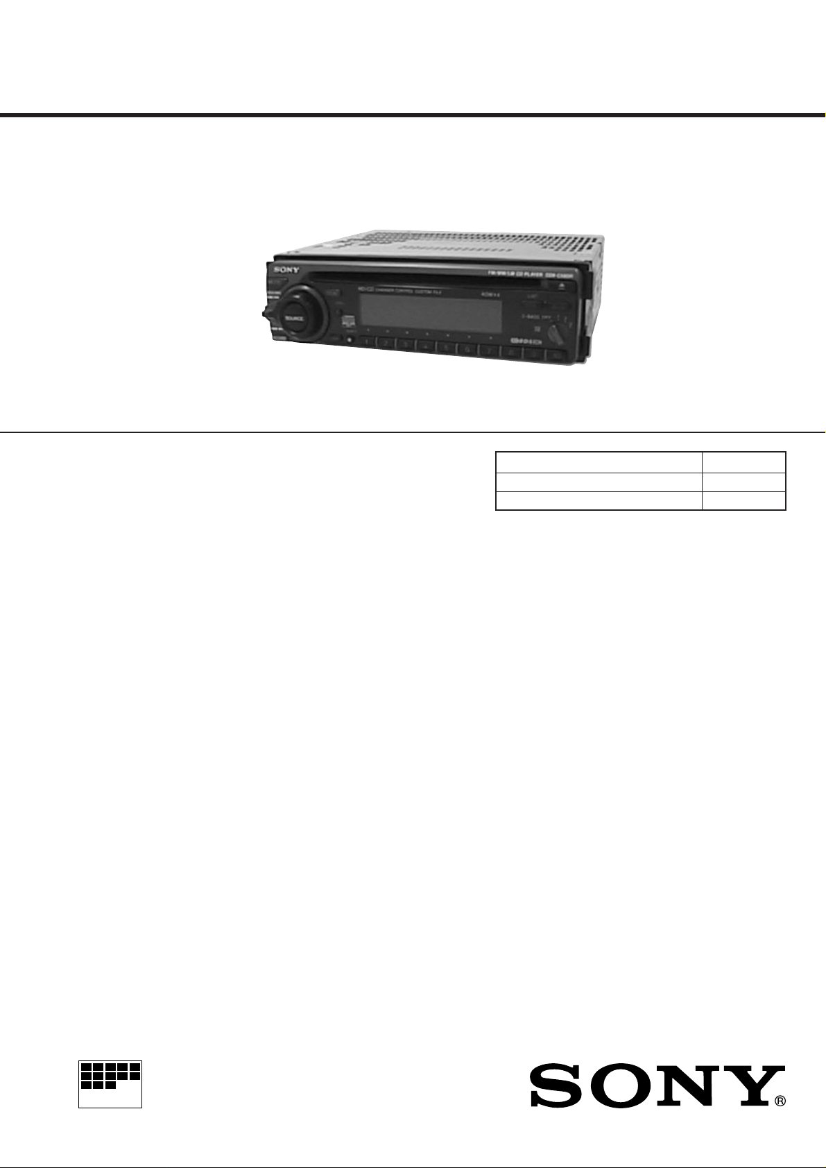
Photo: CDX-C580R
SPECIFICATIONS
AEP Model
UK Model
Model Name Using Similar Mechanism NEW
CD Drive Mechanism Type MG-363T-121
Optical Pick-up Name KSS-520A
CD player section
System Compact disc digital audio
system
Signal-to-noise ratio 90 dB
Frequency response 10 - 20,000 Hz
Wow and flutter Below measurable limit
T uner section
FM
Tuning range 87.5 - 108.0 MHz
Aerial terminal External aerial connector
Intermediate frequency 10.7 MHz
Usable sensitivity 8 dBf
Selectivity 75 dB at 400 kHz
Signal-to-noise ratio 65 dB (stereo),
68 dB (mono)
Harmonic distortion at 1 kHz
0.5% (stereo),
0.3% (mono)
Separation 35 dB at 1 kHz
Frequency response 30 - 15,000 Hz
Capture ratio 2 dB
MW/LW
Tuning range MW : 531 - 1,602 kHz
LW : 153 - 281 kHz
Aerial terminal External aerial connector
Intermediate frequency 10.71 MHz / 450 kHz
Sensitivity MW : 30 µV
LW : 50 µV
Power amplifier section
Outputs Speaker outputs
(sure seal connectors)
Speaker impedance 4 - 8 ohms
Maximum power output 40 W × 4 (at 4 ohms)
General
Outputs Line outputs (2) (CDX-C580R /
C580RW)
Line outputs (1) (CDX-C570R)
Power aerial relay control
lead
Power amplifier control
lead
Telephone ATT control
lead
Tone controls Bass ± 10 dB at 100 Hz
Treble ± 10 dB at 10 kHz
Power requirements 12 V DC car battery
(negative ground)
Dimensions Approx. 178 × 50 × 185 mm
(w/h/d)
Mounting dimensions Approx. 182 × 53 × 162 mm
(w/h/d)
Mass Approx. 1.2 kg
Supplied accessories Parts for installation and
connections (1 set)
Front panel case (1)
Design and specifications are subject to change without
notice.
MICROFILM
FM/MW/LW COMPACT DISC PLAYER
– 1 –
SERVICE NOTE
r
s
NOTES ON CLEANING THE OBJECTIVE LENS
CAUTION
Use of controls or adjustments or performance of procedures other than those specified herein may result in hazardous radiation exposure.
Notes on Chip Component Replacement
• Never reuse a disconnected chip component.
• Notice that the minus side of a tantalum capacitor may be dam-
aged by heat.
NOTES ON HANDLING THE OPTICAL PICK-UP BLOCK OR
BASE UNIT
The laser diode in the optical pick-up block may suffer electrostatic
breakdown because of the potential difference generated by the
charged electrostatic load, etc. on clothing and the human body.
During repair, pay attention to electrostatic breakdown and also use
the procedure in the printed matter which is included in the repair
parts.
The flexible board is easily damaged and should be handled with
care.
NOTES ON LASER DIODE EMISSION CHECK
The laser beam on this model is concentrated so as to be focused on
the disc reflective surface by the objecti ve lens in the optical pic k-up
block. Therefore, when checking the laser diode emission, observe
from more than 30 cm away from the objective lens.
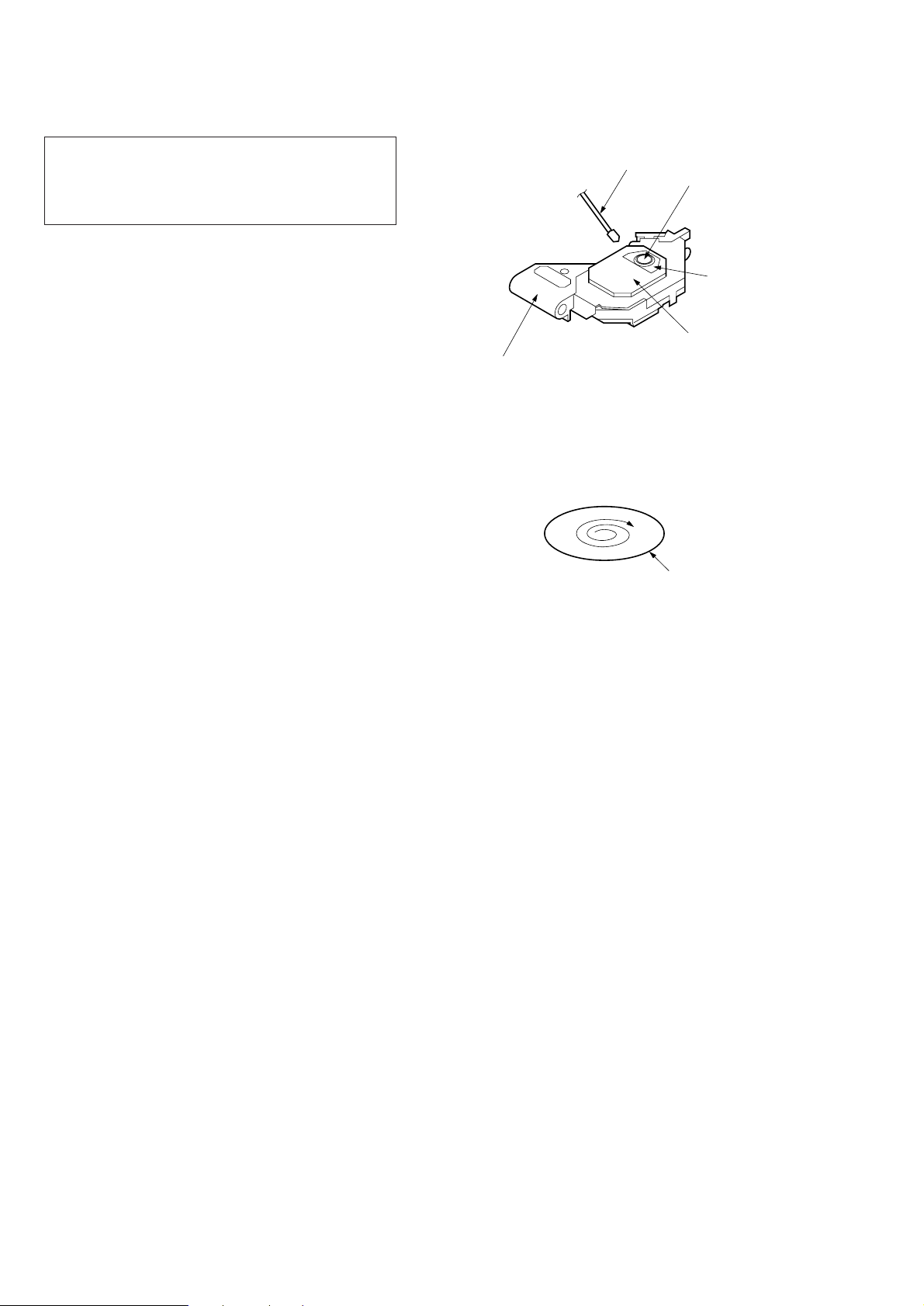
NOTES ON PICK-UP FLEXIBLE BOARD
The pick-up flexible board in this set is secured to the optical pick-up
with an adhesive tape. Once the tape is remov ed, an adhering force
becomes weak, and it cannot be reused.
Therefore, if the optical pick-up is replaced, replace also the pick-up
flexible board with a new one.
cotton swabs
objective lens
2-axis actuato
2-axis cover
slide base
Apply CD lens cleaner B-4 (Part No.:J-2501-000-A) to cotton swabs
(narrow type) (Part No.:J-2501-023-A) to be lightly wet. Use a force
(about 5 g) to make the objective lens in contact with the bottom
lightly, and clean the lens by spirals as following below.
Replace the cotton swab and repeat this cleaning two or three times.
surface of objective len
Notes:
Do not force to push the objective lens. Otherwise, the plate spring
supporting the objective lens will be bent, causing a deteriorated RF
waveform.
Never touch anything other than the objective lens. Otherwise, a
significant deterioration occurs in the RF waveform.
SAFETY-RELATED COMPONENT WARNING!!
COMPONENTS IDENTIFIED BY MARK ! OR DOTTED LINE
WITH MARK ! ON THE SCHEMATIC DIAGRAMS AND IN
THE PARTS LIST ARE CRITICAL TO SAFE OPERATION.
REPLACE THESE COMPONENTS WITH SONY PARTS WHOSE
P ART NUMBERS APPEAR AS SHOWN IN THIS MANU AL OR
IN SUPPLEMENTS PUBLISHED BY SONY.
– 2 –

TABLE OF CONTENTS
1. GENERAL
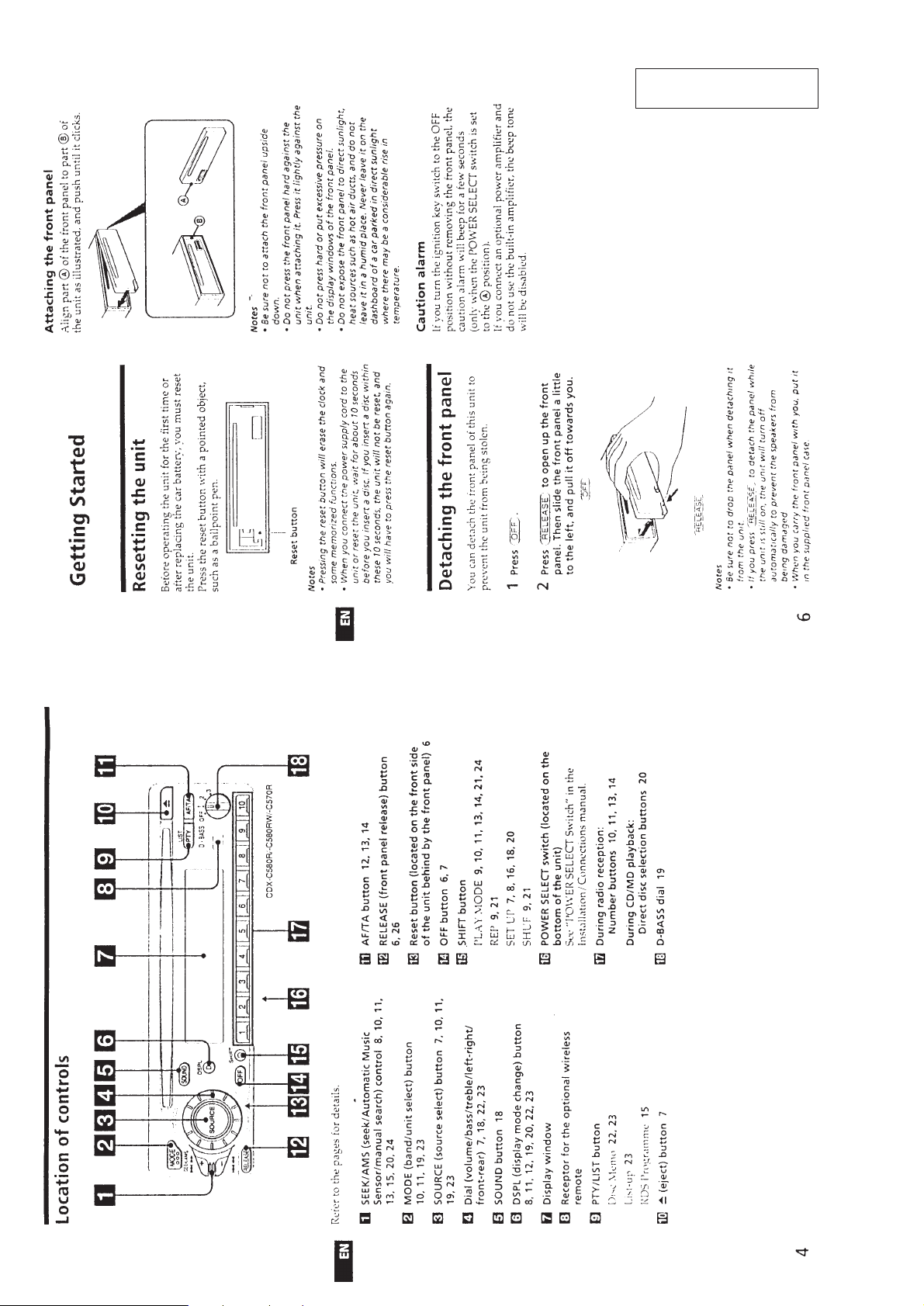
Location of Controls.................................................................. 4
Getting Started........................................................................... 4
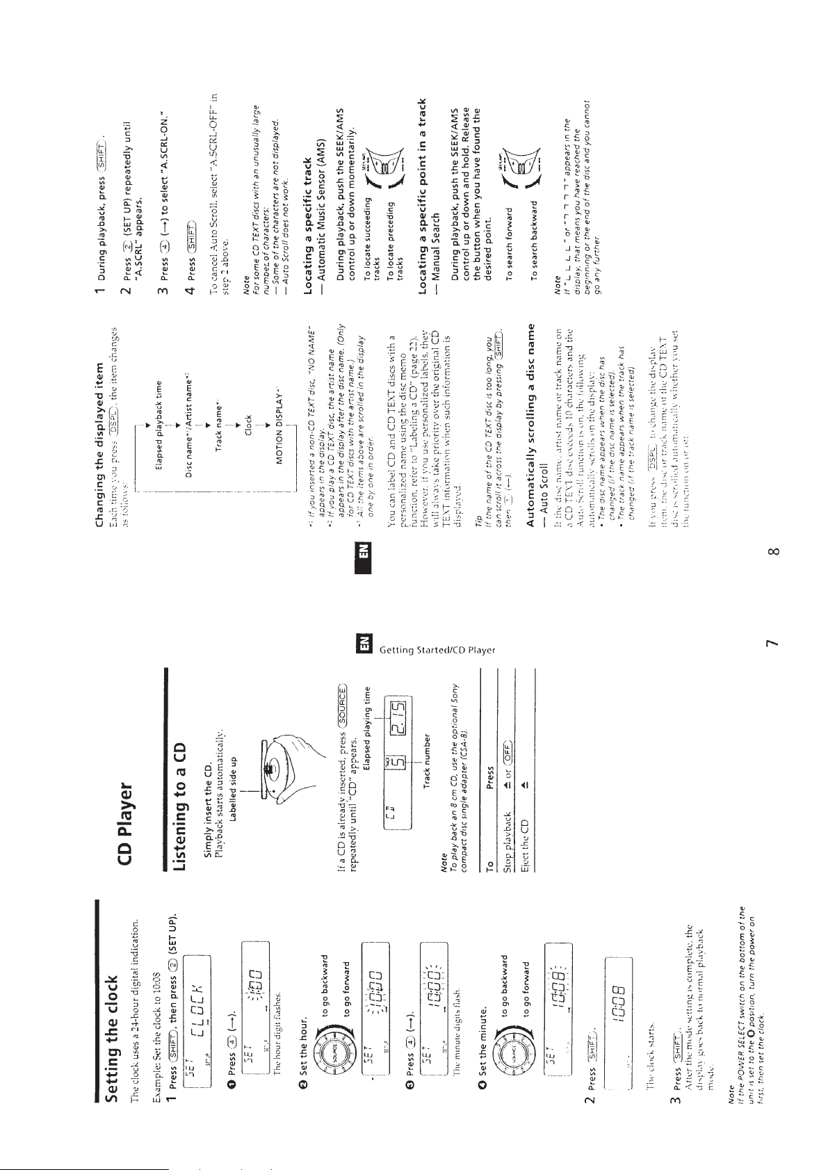
Setting the Clock ....................................................................... 5
CD Player .................................................................................. 5
Radio ......................................................................................... 6
RDS ........................................................................................... 7
Other Functions ......................................................................... 9
CD/MD Unit ............................................................................ 11
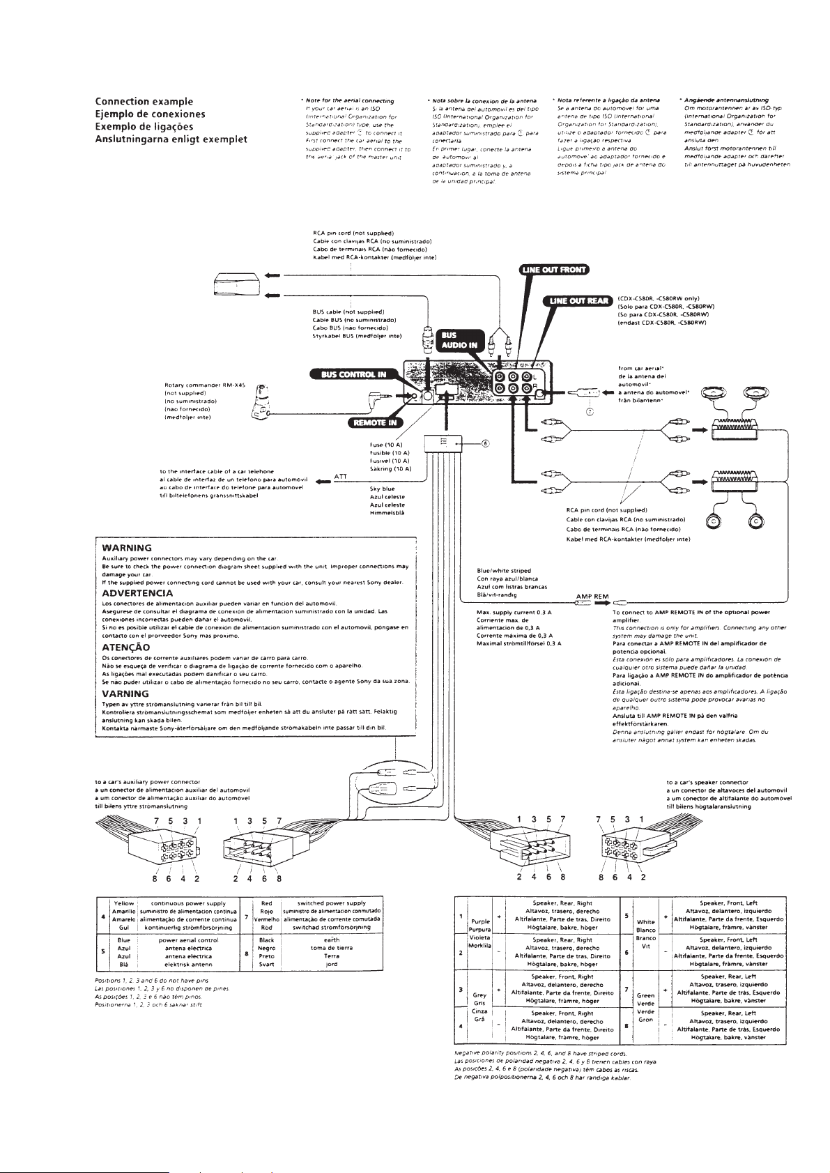
Connections ............................................................................. 14
2. DISASSEMBLY
2-1. Cover Assy .......................................................................... 16
2-2. Front Panel Assy ................................................................. 16
2-3. Sub Panel (1) Assy .............................................................. 17
2-4. CD Mechanism Block ......................................................... 17
2-5. Main Board ......................................................................... 18
2-6. Heat Sink ............................................................................. 18
2-7. Chassis (T) Sub Assy .......................................................... 19
2-8. Lever Assy ........................................................................... 19
2-9. Servo Board......................................................................... 20
2-10. Roller Assy.......................................................................... 20
2-11. Chassis (OP) (O/S) Assy ..................................................... 21
2-12. Optical Pick-up Block ......................................................... 21
3. ELECTRICAL ADJUSTMENTS
Tuner Section........................................................................... 22
CD Section .............................................................................. 25
4. DIAGRAMS
4-1. IC Pin Description............................................................... 26
4-2. Block Diagram –CD Section–............................................. 29
4-3. Block Diagram –Main Section–.......................................... 31
4-4. Circuit Boards Location ...................................................... 33
4-5. Schematic Diagram –CD Mechanism Section– .................. 35
4-6. Printed Wiring Boards –CD Mechanism Section–.............. 37
4-7. Printed Wiring Board –Main Section–................................ 41
4-8. Schematic Diagram –Main Section–................................... 45
4-9. Printed Wiring Board –Display Section–............................ 49
4-10. Schematic Diagram –Display Section–............................... 51
5. EXPLODED VIEWS
5-1. Chassis Section ................................................................... 57
5-2. Front Panel Section ............................................................. 58
5-3. CD Mechanism Section (1) ................................................. 59
5-4. CD Mechanism Section (2) ................................................. 60
5-5. CD Mechanism Section (3) ................................................. 61
6. ELECTRICAL PARTS LIST........................................... 62
– 3 –
SECTION 1
GENERAL
This section extracted from
instruction manual.
– 4 –
– 5 –

– 6 –
– 7 –
– 8 –
– 9 –
– 10 –
– 11 –
– 12 –
– 13 –
– 14 –
– 15 –
SECTION 2
DISASSEMBLY
Note : Follow the disassembly procedure in the n umerical order given.
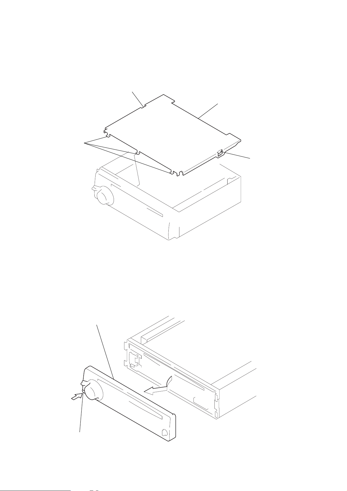
2-1. COVER ASSY
1
claw
3
claws
4
cover assy
2
claw
2-2. FRONT PANEL ASSY
1
2
front panel assy
button (release)
– 16 –
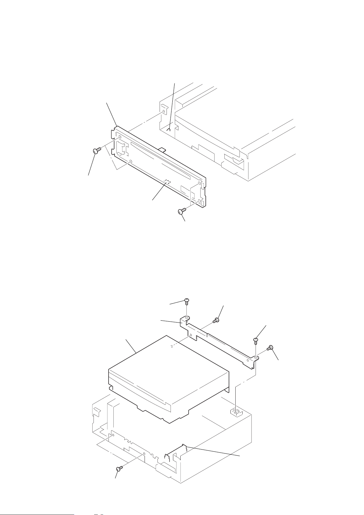
2-3. SUB PANEL (1) ASSY
5
sub panel (1) assy
1
PTT 2.6x6
3
claw
4
claw
2
PTT 2.6x6
2-4. CD MECHANISM BLOCK
5
CD mechanism block
2
PTT 2.6x6
8
bracket (M/D)
7
PTT 2.6x6
3
PTT 2.6x6
6
PTT 2.6x6
1
PTT 2.6x6
– 17 –
4
CNP700
 Loading...