

Page 1
http://getMANUAL.com
CDX-505RF/EXCD-3RF
US Model
SERVICE MANUAL
Ver 1.1 2001.08
Photo: CDX-505RF
Canadian Model
CDX-505RF/EXCD-3RF
AEP Model
UK Model
E Model
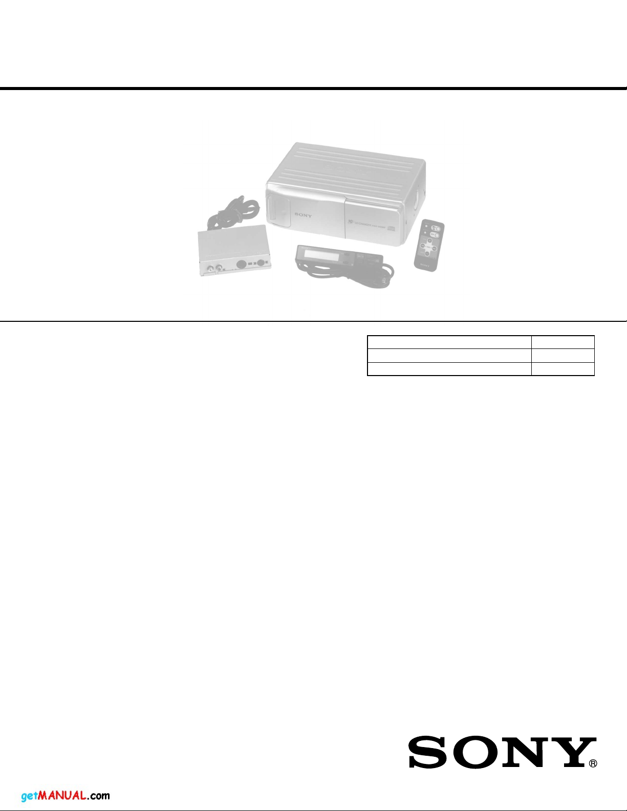
CDX-505RF
CD changer
System Compact disc digital audio system
Laser Diode Properties
Material: GaAlAs
Wavelength: 780 nm
Emission Duration: Continuous
Laser out-put Power: Less than 44.6 µW*
* This output is the value measured at a distance of 200
mm from the objective lens surface on the Optical Pick-
up Block.
Frequency response 10-20,000 Hz
Wow and flutter Below than the measurable limit
Signal-to-noise ratio 94 dB
Outputs terminals BUS control output terminal (8 pin)
Analog audio output terminal (RCA pin)
Current drain 800 mA (at playback)
800 mA (at disc loading/ejecting)
Operating temperature
–10 ºC to +55 ºC (14 ºF to 131 ºF)
Dimensions Approx. 262 × 90 × 181.5 mm
(12 1/8 × 3 5/8 × 7 1/8 in.) (w/h/d)
Mass Approx. 2.1 kg (4 lb. 10 oz.)
SPECIFICATIONS
Hideaway unit / Wired remote (RM-X57) (CDX-505RF) / Wired
remote (RM-X64) (EXCD-3RF) / Wireless remote (RM-X58)
(CDX-505RF ONLY)
Frequency 88.3 MHz/88.5 MHz/
Dimension Hideaway unit :
Mass Hideaway unit:
Supplied accessories
Model Name Using Similar Mechanism NEW
CD Drive Mechanism Type
Optical Pick-up Name
88.7 MHz/88.9 MHz/
89.1 MHz/89.3 MHz/
89.5 MHz/89.7 MHz/
89.9 MHz/ (switchable)
Approx. 124.8 × 30.0 × 99.8 mm
(5 × 1 3/16 × 4 in.) (w/h/d)
Wired remote:
Approx. 148 × 30 × 15 mm
(5 7/8 × 1 3/16 × 9/32 in.) (w/h/d)
Wireless remote:
Approx. 38.4 × 6.4 × 84.4 mm
(1 9/16 × 9/32 × 3 3/8 in.) (w/h/d)
Approx. 330 g (11.64 oz.)
Wired remote:
Approx. 120 g (4.2 oz.)
Wireless remote:
Approx. 20 g (0.7 oz.)
Disc magazine (1)
Parts for installation and connections (1 set)
Lithium battery (CR2025) (1)
MG-250A-137
KSS-521A/J2RP
COMPACT DISC CHANGER SYSTEM
9-925-526-12 Sony Corporation
2001H0500-1 e Vehicle Company
C 2001.8 Shinagawa Tec Service Manual Production Group
Design and specifications subject to change without notice.
Page 2

http://getMANUAL.com
SERVICING NOTES
TABLE OF CONTENTS
1. GENERAL
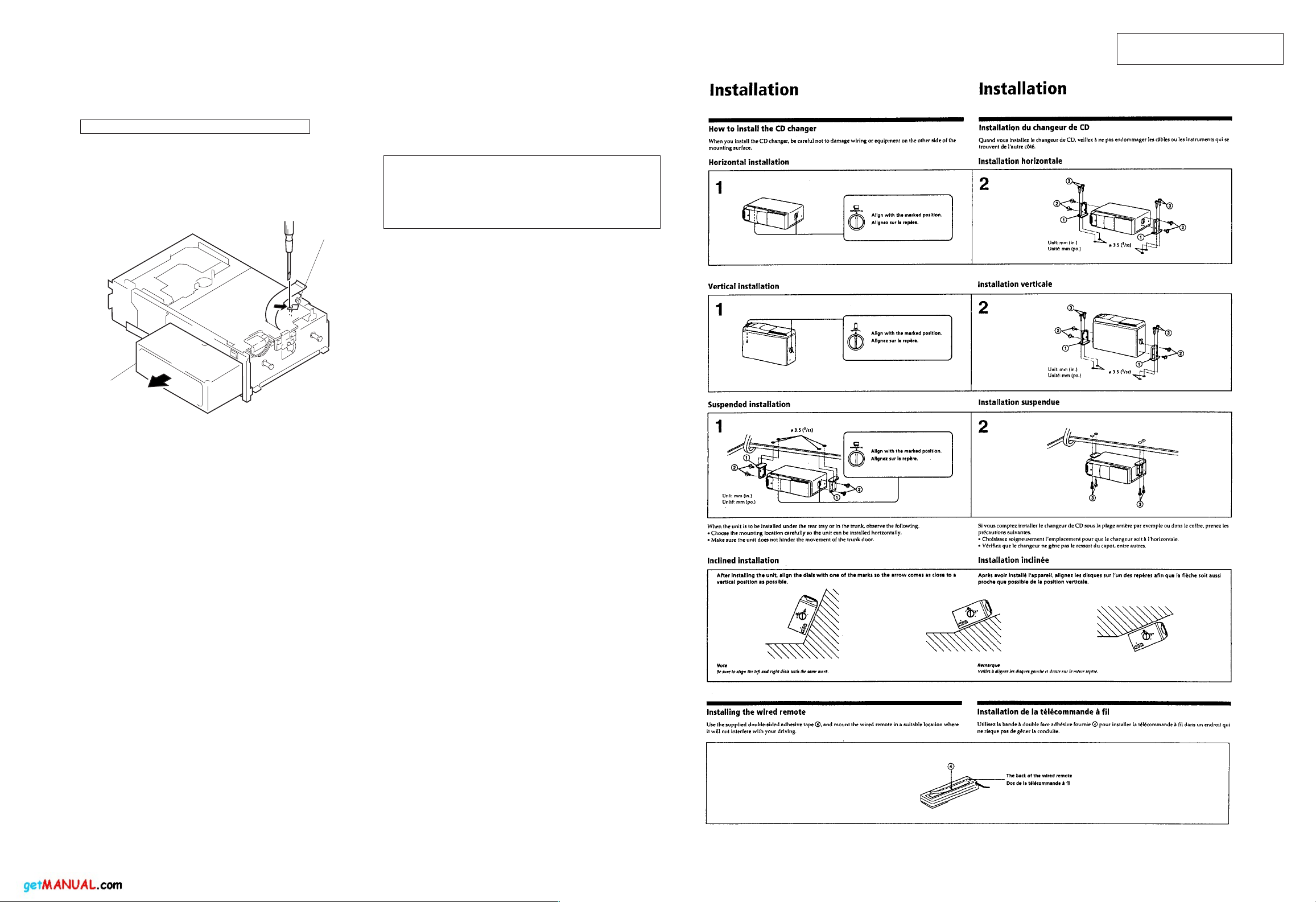
Installation ......................................................................... 4
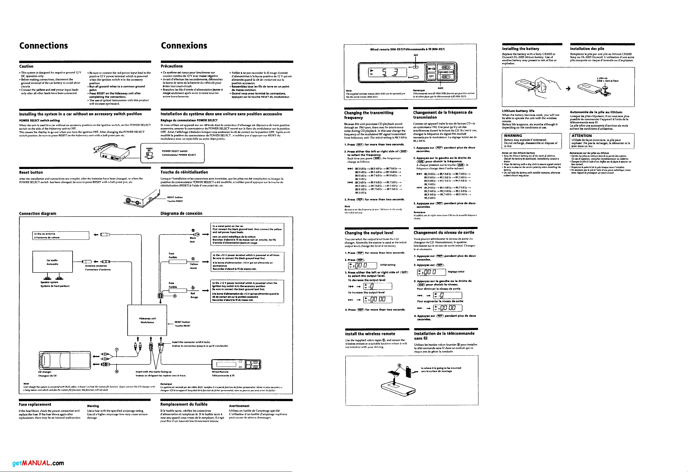
Connections ....................................................................... 5
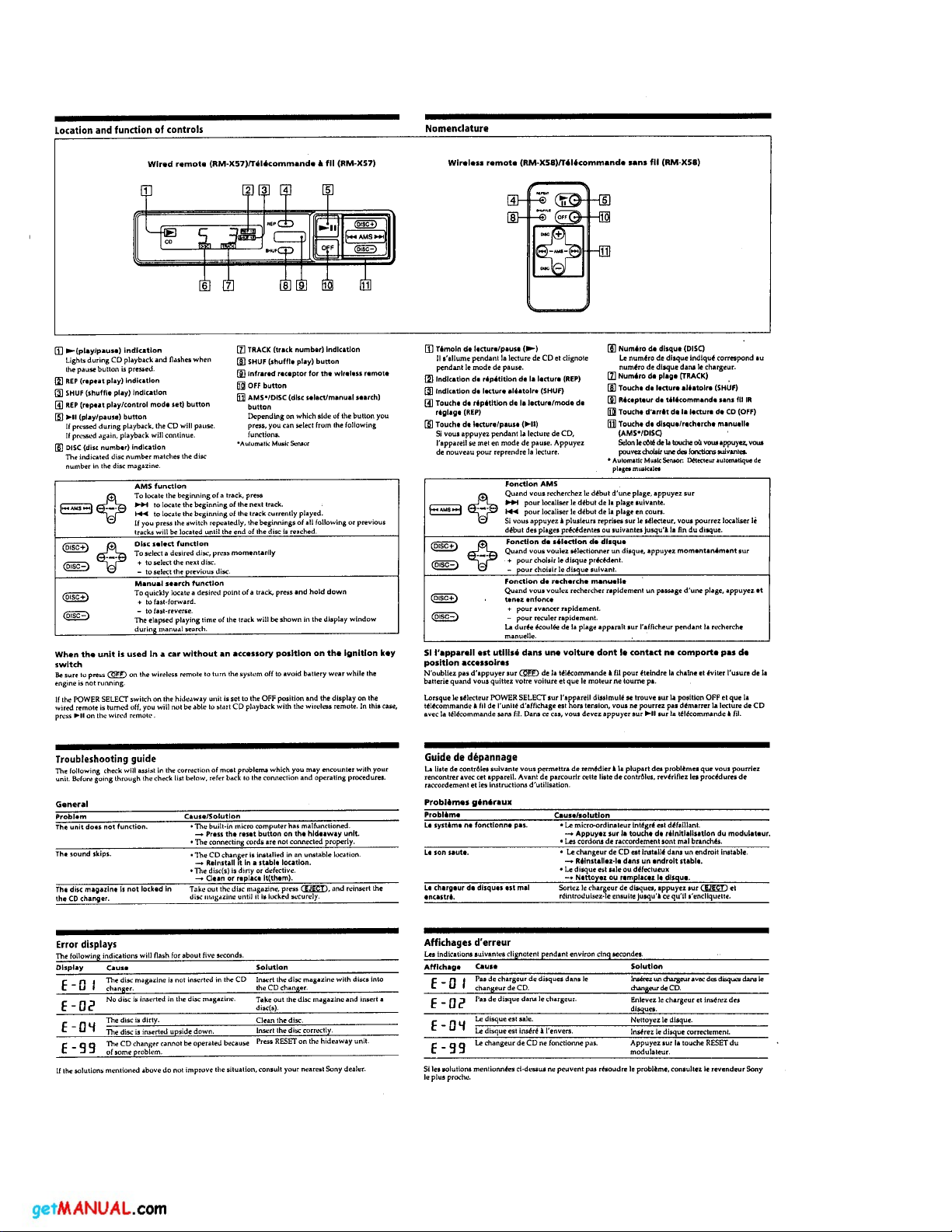
Location and Function of Controls .................................... 8
2. DISASSEMBLY............................................................ 9
3. ELECTRICAL ADJUSTMENTS ........................... 15
4. DIAGRAMS
4-1. Printed W iring Board – RF Section –................................ 17
4-2. Schematic Diagram – RF Section –................................... 19
4-3. Schematic Diagram – MAIN Section –............................. 23
4-4. Printed W iring Board – MAIN Section – .......................... 27
4-5. IC Pin Function Description.............................................. 33
5. EXPLODED VIEWS ................................................... 35
6. ELECTRICAL PARTS LIST .................................... 41
NOTES ON HANDLING THE OPTICAL PICK-UP
BLOCK OR BASE UNIT
The laser diode in the optical pick-up block may suffer electrostatic
breakdown because of the potential difference generated by the
charged electrostatic load, etc. on clothing and the human body.
During repair, pay attention to electrostatic breakdown and also use
the procedure in the printed matter which is included in the repair
parts.
The flexible board is easily damaged and should be handled with
care.
Laser Diode Properites
• Material: GaAlAs
• Wavelength: 780 nm
• Emission Duration: continuous
• Laser Output Power: less than 44.6 µW*
* This output is the value measured at a distance of 200 mm
from the objective lens surface on the Optical Pick-up Block.
CAUTION
Use of controls or adjustments or performance of
procedures other than those specified herein may
result in hazardous radiation exposure.
SAFETY-RELATED COMPONENT WARNING!!
COMPONENTS IDENTIFIED BY MARK ! OR DOTTED
LINE WITH MARK ! ON THE SCHEMATIC DIAGRAMS
AND IN THE PARTS LIST ARE CRITICAL TO SAFE
OPERATION. REPLACE THESE COMPONENTS WITH
SONY PARTS WHOSE PART NUMBERS APPEAR AS
SHOWN IN THIS MANU AL OR IN SUPPLEMENTS PUBLISHED BY SONY.
Flexible Circuit Board Repairing
• Keep the temperature of the soldering iron around 270 ˚C during
repairing.
• Do not touch the soldering iron on the same conductor of the
circuit board (within 3 times).
• Be careful not to apply force on the conductor when soldering or
unsoldering.
Notes on chip component replacement
• Never reuse a disconnected chip component.
• Notice that the minus side of a tantalum capacitor may be dam-
aged by heat.
ATTENTION AU COMPOSANT AYANT RAPPORT
À LA SÉCURITÉ!
LES COMPOSANTS IDENTIFIÉS P AR UNE MARQUE !
SUR LES DIAGRAMMES SCHÉMATIQUES ET LA LISTE
DES PIÈCES SONT CRITIQUES POUR LA SÉCURITÉ
DE FONCTIONNEMENT. NE REMPLACER CES COMPOSANTS QUE PAR DES PIÈCES SONY DONT LES
NUMÉROS SONT DONNÉS DANS CE MANUEL OU
DANS LES SUPPLÉMENTS PUBLIÉS PAR SONY.
– 2 –
Page 3
http://getMANUAL.com
DISC MAGAZINE GETTING OUT PR OCEDURE ON THE
POWER SUPPLY IS OFF
Remove the CASE (LOWER) assembly beforehand
1) Press the lever (stop) assy to arrow direction.
2) Removal the magazine assy.
Note: T ake out the magazine only when the tray is completely within
the magazine. If the disk or tray is sticking out, turn on the
power and eject the magazine.
Lever (stop) ass’y
Magazine ass’y
CAUTION
Danger of explosion if battery is incorrectly replaced.
Replace only with the same or equivalent type recommended by the
manufacturer.
Discard used batteries according to the manufacturer’s instructions.
ADVARSEL!
Lithiumbatteri-Eksplosionsfare ved fejlagtig håndtering.
Udskiftning må kun ske med batteri
af samme fabrikat og type.
Levér det brugte batteri tilbage til leverandøren.
ADVARSEL
Eksplosjonsfare ved feilaktig skifte av batteri.
Benytt samme batteritype eller en tilsvarende type
anbefalt av apparatfabrikanten.
Brukte batterier kasseres i henhold til fabrikantens
instruksjoner.
VARNING
Explosionsfara vid felaktigt batteribyte.
Använd samma batterityp eller en ekvivalent typ som
rekommenderas av apparattillverkaren.
Kassera använt batteri enligt fabrikantens instruktion.
SECTION 1
GENERAL
This section is extracted from
CDX-505RF’s instruction manual.
VAROITUS
Paristo voi räjähtää, jos se on virheellisesti asennettu.
Vaihda paristo ainoastaan laitevalmistajan suosittelemaan tyyppiin.
Hävitä käytetty paristo valmistajan ohjeiden mukaisesti.
– 3 – – 4 –
Page 4
http://getMANUAL.com
– 5 – – 6 –
Page 5

http://getMANUAL.com
– 7 –
Page 6
http://getMANUAL.com
– 8 –
Page 7
http://getMANUAL.com
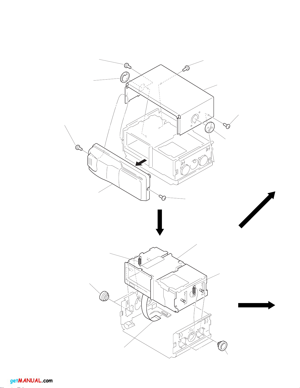
SECTION 2
DISASSEMBLY
Note: Follow the disassembly procedure in the numerical order given.
COVER (UPPER), FRONT PANEL ASS’Y
1
1
screw
(PTT2.6 × 6)
3
lever (FL)
screw
(PTT2.6
×
6)
1
screw
(PTT2.6
×
6)
2
case (upper)
3
1
screw
(PTT2.6
lever (FL)
×
6)
MECHANISM DECK
1
two dampers (250)
4
front panel ass’y
2
spring (FL)
1
screw
(PTT2.6
4
mechanism deck
×
6)
2
spring (FL)
3
jack flexible board
(CN901)
– 9 –
1
two dampers (250)
Page 8
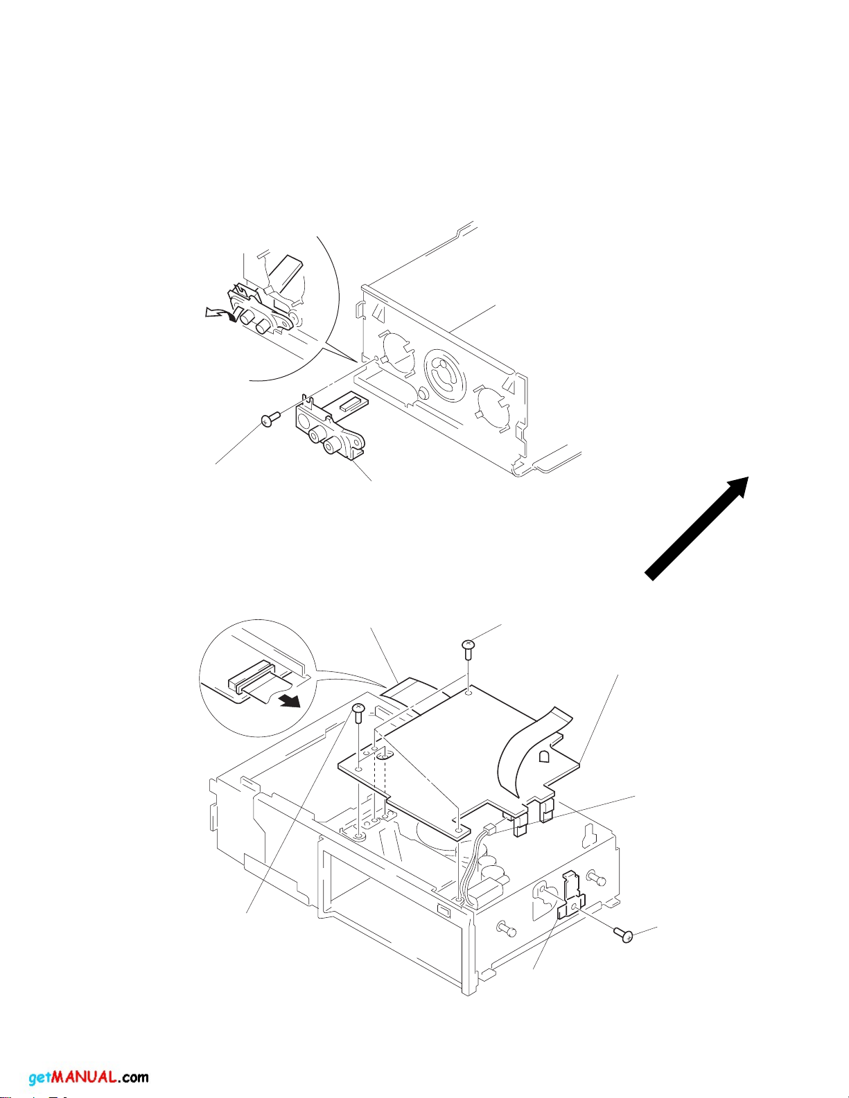
JACK BOARD
http://getMANUAL.com
Remove the jack board of
the arrow.
MAIN BOARD
1
screw
(BVTT2.6 × 5)
2
jack board
1
main flexible board
(CNJ12)
6
three screws
(ground)
7
main board
2
connector
(CNP301)
5
two screws
(P2 × 2.5)
– 10 –
4
heat sink
3
screw
(B2 × 3)
Page 9
ELEVATOR MOTOR ASS’Y (M104)
http://getMANUAL.com
screw
1
(P2 × 2.2)
2
bracket (ELV motor)
3
elevator motor ass’y
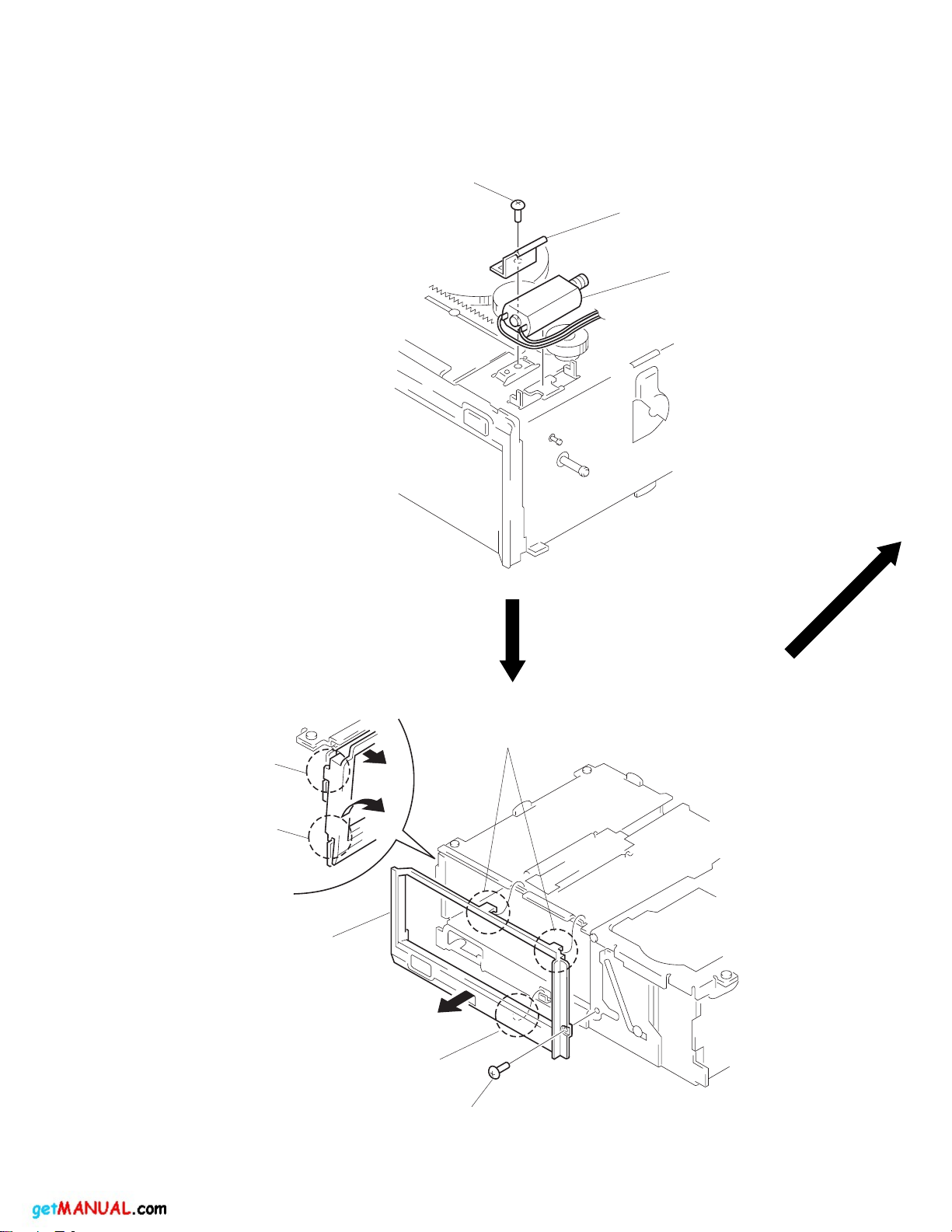
ESCUTCHEON
2
Remove the claw
of the arrow A.
4
Remove the ditch
of the arrow B.
5
Remove the escutcheon
of the arrow C.
B
A
4
C
ditch
1
3
screw
(M2 × 3)
two claws
– 11 –
Page 10
CASE (UPPER) ASS’Y
1
three screws
(B2
×
3)
4
Remove the case
(upper) ass’y of the
arrow B.
http://getMANUAL.com
2
B
A
3
Remove the edge
of the arrow
A
.
1
two screws
(B2 × 3)
CHASSIS ASS’Y
1
screw
(B2 × 3)
3
chassis ass‘y
2
1
two polyethylene washers
1
polyethylene washer
2
– 12 –
Page 11

RF BOARD
5
connector
(CNP52)
2
two screws
(P2 × 2.5)
http://getMANUAL.com
1
OP flexible board
(CNJ11)
3
two screws
×
3)
(P2
4
RF board
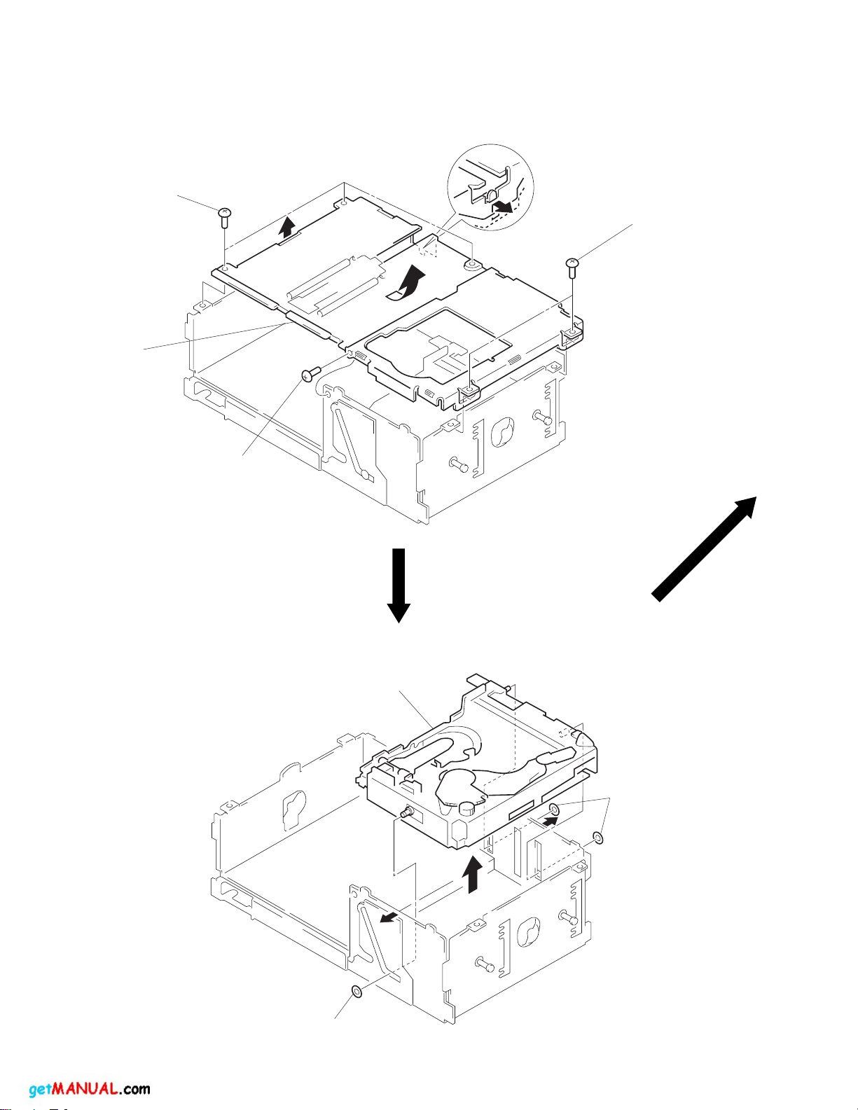
SLED MOTOR ASS’Y (M102), OPTICAL PICK-UP (KSS-521A/J2RP)
2
sled motor ass‘y
4
Turn at the direction of the
arrow, then remove
shaft (sled) ass‘y
1
two screws
(P2 × 3)
5
two connectors
(CNP11, 503)
3
optical pick-up
(KSS-521A/J2RP)
– 13 –
Page 12

http://getMANUAL.com
SW BOARD, SPINDLE MOTOR ASS’Y (M101)
8
two screws
(P1.7
×
2.2)
1
screw
×
2.2)
(P2
7
5
bracket (CP)
3
spring (chucking)
6
4
retainer (disc)
screw
(P2 × 2.2)
2
SW board
CHUCKING MOTOR ASS’Y (M103)
3
bracket
(load motor)
2
two screws (P2 × 2.5)
9
Remove the spindle motor ass‘y (M101)
of the arrow.
4
chucking motor ass‘y
(M103)
1
connector
(CNP51)
– 14 –
Page 13

SECTION 3
n
ELECTRICAL ADJUSTMENTS
http://getMANUAL.com
• FOCUS GAIN ADJUSTMENT
(COARSE ADJUSTMENT)
This adjustment is to be performed when replacing the following
parts.
• Optical Pick-up Block
• RV14
Procedure:
[RF BOARD] – Conductor Side –
CNJ12
IC51
RV14
1. Set RV14 (RF board) to the standard position.
2. Check that there is not an abnormal amount of operation noise
(white noise) from the 2-axis devise. If there is, turn RV14
slightly clockwise.
IC11
• When gain is lowered...
The set does not play because of no focus operation.
• When gain is highered...
Operation noise is heard due to a scratch or a dust, then operation will be unstable.
[RF BOARD] – Conductor Side –
MIN side
(low gain)
MAX side
(high gain)
RV14 standard positio
– 15 – – 16 –
Page 14

http://getMANUAL.com
Page 15

http://getMANUAL.com
Page 16

http://getMANUAL.com
Page 17

http://getMANUAL.com
Page 18

• IC Block Diagrams
IC101 CXD2530Q
TES6
VDD
VSS
EXCK
79 78
80
77
NC
81
82
VSS
VDD
83
NC
84
85
TES7
86
NC
VSS
87
XVDD
88
XTAI
89
XTAO
90
91
XVSS
92
VSS
NC
93
TES8
94
NC
95
VDD
96
97
VSS
98
NC
NC
XRST
99
100
TIMING
LOGIC
SBSO
SCOR
76 75 74
INTERFACE
WFCK
TES5
EMPH
73 72
EFM
DEMODULATOR
SUB CODE
PROCESSOR
CPU
http://getMANUAL.com
DOUT
C4M
FSTT
XTSL
MNT0
MNT1
MNT3
XROF
C2PO
RFCK
GFS
XPCK
69 68
70
71
66 65 64
67
ERROR
CORRECTOR
16K RAM
SERVO
AUTO
SEQUENCER
63 62
59 58
60
61
D / A
INTERFACE
DIGITAL OUT
DIGITAL CLV
XUGF
GTOP
57
VDD
VSS
56 55 54
TES4
BCK
TES3
535251
ASYMMETRY
CORRECTOR
DIGITAL
PLL
CLOCK
GENERATOR
PCMD
OSC
TES9
LRCK
50
49
WDCK
48
ASYE
47
ASYO
ASYI
46
BIAS
45
RF
44
AVDD
43
42
CLTV
AVSS
41
40
FILI
39
FILO
PCO
38
VCTL
37
V16M
36
35
VCKI
34
VPCO1
33
VPCO2
32
TES1
31
TES0
1 234
VDD
VSS
56789 10
TES2
LMUT
RMUT
IC204 BA8272F-E2
VCC
BUS ON
LINK OFF
CLK OUT
GND
BUS ON IN
11
5 6 7
4
VREF
BUS CLK
14 13 12
2 3
1
BUS ON OUT
CKOUT
DATA OUT
10
BUS DATA
SQCK
SQSO
SENS
DATA
DATA IN
12 13
11
XLAT
RESET
89
RESET
SWITCH
BUS RESET
CLOK
14
SEIN
15 16 17
CNIN
DATO
XLTO
18 19 20
CLKO
SPOA
SPOB
21
SPOC
22 23
SPOD
XLON
FOK
24
VDD
25 26 27
VSS
MON
28 29 30
MDP
MDS
LOCK
PWMI
– 31 –
Page 19

http://getMANUAL.com
IC301 BA6287F
1
OUT1
2
VM
DRIVER DRIVER
TSD
3
VCC
POWER
SAVE
4
FIN
CONTROL LOGIC
IC401 TC9404FN-EL
SH
LRCK
BCK
8
GND
7
OUT2
6
VREF
5
RIN
DATA
INTERFACE
CIRCUIT
DIGITAL FILTER CIRCUIT
ATTENUATOR OPERATIONAL CIRCUIT
DEEMPHASIS FILTER CIRCUIT
D-∆ MODULATION CIRCUIT
TEST
CIRCUIT
2 3
1
T1
VDD
P/S
ATT
HS
(SM)
20
21222324
MICROCOMPUTER
INTERFACE
CIRCUIT
OUTPUT
CIRCUIT
ANALOG
FILTER
5 6 7 8 9
4
RO
VDA
LA
(BS)
VR
VDXXOXI
OSC
TIMING
GENERATOR
OUTPUT
CIRCUIT
ANALOG
FILTER
GNDA
LO
(EMP)
19 18 17 16 15 14 13
GNDA
GNDX
10
11
ZD
VDA
MCK
12
GNDD
– 32 –
Page 20

http://getMANUAL.com
SECTION 6
DIAGRAMS
4-5. IC PIN FUNCTION DESCRIPTION
MAIN BOARD IC302 CXP84124-066Q (SYSTEM CONTROLLER)
Pin No. Pin Name I/O Function
1 LIM.SW I Input of limit switch
2 BUSON I Input of Bus on control signal from SONY bus interface (IC204) “H”: Bus on
3 EJECT I Input of EJECT key (SW303) “H”: Eject on
4 LOAD 1 I Input of LOAD OUT switch
5 LOAD 2 I Input of LOAD IN switch
6 A.MUTE O Output of audio output mute on/off control signal “H”: Mute on
7 EMPH O Output of emphasis mode for disc playing “L”: on
8 CH.R O
Output of control signal to
9 CH.F O
10 ——Not used
11 ELV.R O Output of control signal to elevator motor drive (IC301)
12 ELV.ON O Output of mechanical deck power supply control signal “H”: on
13 CD RST O Servo system resetting
14 CD ON O Output of servo power supply control signal “H”: on
15 GBON — Not used
16 EEON — Not used
17-23 ——Not used
24 TEST1 I
25-29 ——Not used
30 RESET I Input of system reset signal “L”: Reset
31 EXTAL I Input of system clock (8 MHz)
32 XTAL O Output of system clock (8 MHz)
33 VSS — Ground pin
34 TX — Not used
35 TEX I Connected to ground
36 AVSS — Ground pin of A/D converter
37 AVREF I Input of A/D converter reference voltage
38 ATRIBT I Selection of custom file, D-BASS, etc.
39 MCK I Input of signal for fine adjustment of elevator position
40 EHS I Input of elevator position (RV302)
41 HTMP — Not used
42 ——Not used
43 MODE1 O Output of D-BASS control signal Not used
44 MODE2 O Output of D-BASS control signal Not used
45 MODE3 O Output of D-BASS control signal Not used
46, 47 ——Not used
48 SCK O Output of serial clock signal from SONY bus interface (IC204)
49 SI I Input of serial data signal from SONY bus interface (IC204)
50 SO O Output of serial data signal to SONY bus interface (IC204)
the chucking motor drive (IC52)
Automatic adjustment selection “L”: Automatic adjustment “H”: Manual adjustment (Solder across
the BP302 terminal)
CH.R L H H
CH.F H L H
FWD REV Brake
Forward : Load chucking
Reverse : Save
– 33 –
Page 21

http://getMANUAL.com
Pin No. Pin Name I/O Function
51 SQCLK O Output of clock signal to CXD2530Q (IC101)
52 SUBQ I Input of subcode Q data signal from CXD2530Q (IC101)
53 ——Not used
54 ——Connected to the power supply
55 MGLK I Input of magazine eject completion detect switch (SW301) “L”: Eject completed
56 SCOR I Input of subcode sync detect signal from CXD2530Q (IC101)
57 SENS2 I Input of sense signal from CXA1992AR (IC11)
58 PWM O Output of PWM for control to elevator motor drive (IC301)
59 ——Not used
60 MAG.SW I Input of magazine detection switch (SW302) “L”: Magazine detected
61 BUCHECK I Input of backup detection detection “H”: Backup on
62 W.UP I Input of Bus on or EJECT key
63 C.OUT I Input of track counting signal
64 EEDATA I/O Input/output of data signal to E2PROM (IC303) Not used
65 EECLK O Output of clock signal to E2PROM (IC303) Not used
66 EEINIT I Input of OK signal from E2PROM (IC303) fixed at “L”
67 ——Not used
68 SINGLE I Selection of single mode “L”: Single CD playing
69 FOK I Input of focus initialize signal from CXA1992AR (IC11) and CXD2530Q (IC101)
70 GFS I Input of guard frame sync signal from CXD2530Q (IC101)
71 SENS1 I Input of sense signal from CXD2530Q (IC101)
72 VDD — Power supply
73 ——Connected to the power supply
74 CD CLK O Output of serial data transfer clock signal to CXD2530Q (IC101)
75 CD XLT O Output of latch signal to CXD2530Q (IC101)
76 CD DATA O Output of serial data signal to CXD2530Q (IC101)
77-80 ——Not used
– 34 –
Page 22

http://getMANUAL.com
NOTE:
• -XX and -X mean standardized parts, so they
may have some difference from the original
one.
• Color Indication of Appearance Parts
Example:
KNOB, BALANCE (WHITE) . . . (RED)
↑↑
Parts Color Cabinet's Color
(1) COVER SECTION
7
#2
SECTION 5
EXPLODED VIEWS
• Items marked “*” are not stocked since they
are seldom required for routine service. Some
delay should be anticipated when ordering
these items.
• The mechanical parts with no reference num-
ber in the exploded views are not supplied.
• Hardware (# mark) list and accessories and
packing materials are given in the last of the
electrical parts list.
13
#3
11
9
#2
12
#2
14
The components identified by mark
! or dotted line with mark ! are
critical for safety.
Replace only with part number
specified.
Les composants identifiés par une
marque ! sont critiquens pour la
sécurité.
Ne les remplacer que par une pièce
portant le neméro spécifié.
#2
13
Ver 1.1
#2
8
21
5
#1
4
18
17
3
1
19
6
Ref. No. Part No. Description Remark
1 3-010-104-01 DAMPER (250)
* 2 3-010-097-01 COVER (LOWER) (GOLD) (CDX-505RF)
* 2 3-010-097-21 COVER (LOWER) (BLACK) (EXCD-3RF)
3 1-664-628-11 JACK FLEXIBLE BOARD
* 4 1-664-631-11 JACK BOARD
MG-250A-137
12
20
15
16
18
#4
1
2
Ref. No. Part No. Description Remark
* 11 3-010-107-01 HEAT SINK
12 3-010-103-01 SPRING (FL)
13 3-010-101-01 LEVER (FL) (GOLD) (CDX-505RF)
13 3-010-101-11 LEVER (FL) (BLACK) (EXCD-3RF)
* 14 3-010-096-01 COVER (UPPER) (GOLD) (CDX-505RF)
5 X-3373-217-1 DOOR ASSY (SILVER) (CDX-505RF)
5 X-3373-488-1 DOOR ASSY (BLACK) (EXCD-3RF)
* 6 3-012-790-01 SHEET (F), PROTECTION
7 3-010-098-21 PANEL, FRONT (SILVER) (CDX-505RF)
7 3-010-098-41 PANEL, FRONT (BLACK) (EXCD-3RF)
8 3-012-388-01 SCREW (M 2X3)
* 9 3-010-105-01 ESCUTCHEON
* 10 3-010-106-01 BUTTON (EJ) (6)
* 14 3-010-096-21 COVER (UPPER) (BLACK) (EXCD-3RF)
* 15 A-3309-926-A MAIN BOARD, COMPLETE
16 1-664-627-11 MAIN FLEXIBLE BOARD
17 3-913-406-01 SCREW (GROUND)
18 X-3373-215-1 ARM (FL) ASSY
* 19 3-013-658-01 SHEET (FJ), PROTECTION
* 20 3-014-434-01 COLLAR (PRINT)
21 3-014-390-01 SPRING (PWM), TENSION
– 35 –
Page 23

Ver 1.1
(2) MECHANISM DECK SECTION-1
(MG-250A-137)
#3
http://getMANUAL.com
56
55
55
57
#5
54
61
#3
53
#3
58
60
51
59
60
52
51
Ref. No. Part No. Description Remark
51 4-965-759-01 WASHER, POLYETHYLENE1
* 52 X-3373-239-1 SLIDER (R) ASSY
53 3-010-244-01 SPRING (STOPPER. UPPER)
* 54 X-3373-243-1 CASE (UPPER) ASSY
55 3-010-217-01 SPRING (EJECT)
* 56 3-010-162-01 LEVER (EJECT)
* 57 3-011-998-01 BRACKET (STOPPER UPPER)
– 36 –
62
63
Ref. No. Part No. Description Remark
* 58 3-010-240-01 SLIDER (L)
59 3-011-997-01 SPRING (STOPPER LOWER)
60 3-578-224-00 WASHER
61 3-736-073-01 SLIDER, POLYETHYLENE
62 3-014-433-01 COLLAR (SLIDER)
63 3-920-362-01 SCREW (ESCUTCHEON)
Page 24

http://getMANUAL.com
(3) MECHANISM DECK SECTION-2
(MG-250A-137)
#13
111
M104
104
105
Ver 1.1
113
#5
103
106
#14
112
116
115
114
107
109
110
108
102
101
Ref. No. Part No. Description Remark
* 101 X-3373-223-1 CASE (LOWER) ASSY
102 3-010-266-01 SPRING (STOP LEVER), TENSION
* 103 3-010-250-01 BRACKET (ELV MOTOR)
104 3-736-073-01 SLIDER, POLYETHYLENE
105 3-010-211-01 GEAR (WORM ELV)
106 3-336-319-01 RING, RETAINING
107 3-010-175-01 GEAR (ELV 1)
108 3-010-239-01 GEAR (ELV 2)
109 3-362-579-01 RING, RETAINING
– 37 –
Ref. No. Part No. Description Remark
110 3-010-249-01 GEAR (ELV 3)
* 111 3-016-916-01 BRACKET (WORM RETAINER)
* 112 3-014-681-01 SHAFT (WORM RETAINER)
* 113 3-014-685-01 SPACER (MO)
* 114 3-014-389-01 SPACER (LSW)
* 115 3-014-683-01 SPACER (PB)
116 3-015-483-00 SPACER
M104 A-3301-123-A ELJ MOTOR ASSY (ELEVATOR)
Page 25

(4) MECHANISM DECK SECTION-3
(MG-250A-137)
http://getMANUAL.com
#8
168
159
160
#5
167
161
162
163
162
164
#12
153
166
154
152
155
156
M103
151
#4
Ref. No. Part No. Description Remark
* 151 3-010-269-01 BRACKET (LOAD MOTOR)
* 152 X-3373-230-1 BASE (WORM) ASSY
* 153 3-010-270-01 COVER (MOTOR L)
154 3-321-813-01 WASHER, COTTER POLYETHYLENE
155 3-010-248-01 GEAR (WORM LOAD 1)
156 3-573-936-00 STOPPER, REEL
157 3-010-255-01 ARM (LSW)
* 158 A-3309-786-A RF BOARD, COMPLETE
159 A-3228-939-A MAIN ASSY, CHASSIS (ELV)
160 3-010-242-01 RETAINER (DISC)
#4
#8
157
#7
165
Ref. No. Part No. Description Remark
* 161 3-010-243-01 BRACKET (CP)
162 3-736-073-01 SLIDER, POLYETHYLENE
163 3-010-251-01 ARM (CONVERSION AB)
* 164 X-3373-232-1 LEVER (LOCK 3) ASSY
165 3-918-103-01 SCREW +P2 × 3
166 X-3373-552-1 GEAR (LOAD 1) ASSY
167 3-010-254-01 SHAFT (ROTARY PREVENTION C)
168 3-010-253-01 GEAR (LO MINI)
M103 A-3291-953-A MOTOR ASSY, EL (CHUCKING)
158
– 38 –
Page 26

http://getMANUAL.com
(5) MECHANISM DECK SECTION-4
(MG-250A-137)
205
#11
207
202
203
#5
204
#9
201
206
208
#5
209
M101
211
#5
210
#10
M102
Ref. No. Part No. Description Remark
201 X-3373-229-1 BASE (SLED) ASSY
202 3-010-258-01 GEAR (SLED MID)
203 3-573-936-00 STOPPER, REEL
204 A-3291-958-A SHAFT (SLED) ASSY
* 205 1-664-104-11 SW BOARD
206 3-010-263-01 DETENT (SHAFT THRUST)
* 207 X-3373-225-1 BASE (OP) ASSY
– 39 –
Ref. No. Part No. Description Remark
208 3-010-261-01 SHAFT (GUIDE S)
! 209 8-820-010-05 OPTICAL PICK-UP KSS-521A/J2RP
210 1-664-626-11 OP FLEXIBLE BOARD
211 3-010-262-01 DETENT (SLED)
M101 A-3301-067-A MOTOR (SP) ASSY, D.C. (SPINDLE)
M102 A-3291-955-A MOTOR SUB ASSY, SLED
The components identified by
mark ! or dotted line with
mark ! are critical for safety.
Replace only with part number
specified.
Les composants identifiés par une
marque ! sont critiques pour la
sécurité.
Ne les remplacer que par une pièce
portant le neméro spécifié.
Page 27

(6) HIDEAWAY UNIT SECTION
http://getMANUAL.com
F1
251
F2
252
Ref. No. Part No. Description Remark
251 1-473-879-11 RF UNIT (HIDEAWAY) (CDX-505RF)
251 1-473-881-21 RF UNIT (HIDEAWAY) (EXCD-3RF)
252 1-777-519-11 CORD (WITH CONNECTOR)
– 40 –
Ref. No. Part No. Description Remark
F1 1-532-416-00 FUSE (3.15A)
F2 1-532-360-XX FUSE (1A)
Page 28

http://getMANUAL.com
SECTION 6
ELECTRICAL PARTS LIST
JACK MAIN
NOTE:
• Due to standardization, replacements in the
parts list may be different from the parts specified in the diagrams or the components used on
the set.
• -XX and -X mean standardized parts, so they
may have some difference from the original one.
• RESISTORS
All resistors are in ohms.
METAL: Metal-film resistor.
METAL OXIDE: Metal oxide-film resistor.
F: nonflammable
• Items marked “*” are not stocked since they
are seldom required for routine service.
Some delay should be anticipated when ordering these items.
Ref. No. Part No. Description Remark
* 1-664-631-11 JACK BOARD
**********
< CAPACITOR >
C901 1-163-009-11 CERAMIC CHIP 0.001uF 10% 50V
C903 1-163-038-00 CERAMIC CHIP 0.1uF 25V
C904 1-163-009-11 CERAMIC CHIP 0.001uF 10% 50V
< CONNECTOR >
CN901 1-779-077-11 PLUG, CONNECTOR (SONY BUS/AUDIO OUT)
CN901 1-779-077-21 PLUG, CONNECTOR (SONY BUS/AUDIO OUT)
CNJ901 1-778-775-21 CONNECTOR, FPC 13P
< FERRITE BEAD >
FB901 1-500-445-21 BEAD, FERRITE (CHIP)
FB902 1-500-445-21 BEAD, FERRITE (CHIP)
FB903 1-500-445-21 BEAD, FERRITE (CHIP)
< IC LINK >
IC901 1-532-686-21 LINK, IC (2.7A)
************************************************************
* A-3309-926-A MAIN BOARD, COMPLETE
*********************
* 3-011-852-01 HOLDER (REG)
< CAPACITOR >
C101 1-163-038-00 CERAMIC CHIP 0.1uF 25V
C102 1-163-251-11 CERAMIC CHIP 100PF 5% 50V
C103 1-163-011-11 CERAMIC CHIP 0.0015uF10% 50V
C104 1-163-035-00 CERAMIC CHIP 0.047uF 50V
C105 1-163-038-00 CERAMIC CHIP 0.1uF 25V
C106 1-164-182-11 CERAMIC CHIP 0.0033uF10% 50V
C107 1-164-232-11 CERAMIC CHIP 0.01uF 50V
C108 1-163-038-00 CERAMIC CHIP 0.1uF 25V
C109 1-126-513-11 ELECT 47uF 20% 6.3V
C110 1-163-038-00 CERAMIC CHIP 0.1uF 25V
• SEMICONDUCTORS
In each case, u: µ, for example:
uA. . : µA. . uPA. . : µPA. .
uPB. . : µPB. . uPC. . : µPC. .
uPD. . : µPD. .
• CAPACITORS
uF: µF
• COILS
uH: µH
(EXCEPT EXCD-3RF:US)
(EXCD-3RF:US)
The components identified by mark
! or dotted line with mark ! are
critical for safety.
Replace only with part number
specified.
Les composants identifiés par une
marque ! sont critiquens pour la
sécurité.
Ne les remplacer que par une pièce
portant le neméro spécifié.
When indicating parts by reference
number, please include the board.
Ref. No. Part No. Description Remark
C120 1-163-038-00 CERAMIC CHIP 0.1uF 25V
C121 1-163-038-00 CERAMIC CHIP 0.1uF 25V
C122 1-163-038-00 CERAMIC CHIP 0.1uF 25V
C123 1-163-038-00 CERAMIC CHIP 0.1uF 25V
C124 1-163-038-00 CERAMIC CHIP 0.1uF 25V
C125 1-163-009-11 CERAMIC CHIP 0.001uF 10% 50V
C201 1-124-589-11 ELECT 47uF 20% 16V
C202 1-126-513-11 ELECT 47uF 20% 6.3V
C203 1-163-038-00 CERAMIC CHIP 0.1uF 25V
C204 1-115-466-00 ELECT 1000uF 20% 16V
C205 1-163-038-00 CERAMIC CHIP 0.1uF 25V
C206 1-124-589-11 ELECT 47uF 20% 16V
C207 1-124-589-11 ELECT 47uF 20% 16V
C208 1-164-346-11 CERAMIC CHIP 1uF 16V
C209 1-124-589-11 ELECT 47uF 20% 16V
C210 1-125-701-11 CAPACITOR 0.047F 5.5V
C211 1-163-038-00 CERAMIC CHIP 0.1uF 25V
C212 1-164-346-11 CERAMIC CHIP 1uF 16V
C213 1-164-346-11 CERAMIC CHIP 1uF 16V
C214 1-163-038-00 CERAMIC CHIP 0.1uF 25V
C302 1-163-038-00 CERAMIC CHIP 0.1uF 25V
C303 1-126-513-11 ELECT 47uF 20% 6.3V
C304 1-163-038-00 CERAMIC CHIP 0.1uF 25V
C305 1-163-038-00 CERAMIC CHIP 0.1uF 25V
C306 1-163-038-00 CERAMIC CHIP 0.1uF 25V
C308 1-163-038-00 CERAMIC CHIP 0.1uF 25V
C401 1-124-589-11 ELECT 47uF 20% 16V
C402 1-163-038-00 CERAMIC CHIP 0.1uF 25V
C403 1-163-038-00 CERAMIC CHIP 0.1uF 25V
C404 1-126-513-11 ELECT 47uF 20% 6.3V
C405 1-126-513-11 ELECT 47uF 20% 6.3V
C406 1-163-038-00 CERAMIC CHIP 0.1uF 25V
C407 1-126-157-11 ELECT 10uF 20% 16V
C408 1-163-038-00 CERAMIC CHIP 0.1uF 25V
C409 1-126-513-11 ELECT 47uF 20% 6.3V
C410 1-126-157-11 ELECT 10uF 20% 16V
C411 1-126-157-11 ELECT 10uF 20% 16V
C412 1-163-009-11 CERAMIC CHIP 0.001uF 10% 50V
C413 1-163-251-11 CERAMIC CHIP 100PF 5% 50V
C414 1-163-251-11 CERAMIC CHIP 100PF 5% 50V
– 41 –
Page 29

MAIN
http://getMANUAL.com
Ref. No. Part No. Description Remark
C415 1-163-009-11 CERAMIC CHIP 0.001uF 10% 50V
C501 1-163-009-11 CERAMIC CHIP 0.001uF 10% 50V
C502 1-163-029-11 CERAMIC CHIP 0.0047uF50V
C503 1-163-038-00 CERAMIC CHIP 0.1uF 25V
< CONNECTOR >
CNJ101 1-770-351-11 CONNECTOR, FPC 26P
CNJ201 1-770-350-21 CONNECTOR, FPC 13P
CNP301 1-580-055-21 PIN, CONNECTOR 2P
< DIODE >
D201 8-719-210-33 DIODE EC10DS2
D202 8-719-210-33 DIODE EC10DS2
D203 8-719-801-78 DIODE 1SS184
D204 8-719-422-64 DIODE MA8062-M
D205 8-719-038-48 DIODE 1SS319 (TE85R)
D206 8-719-801-78 DIODE 1SS184
D207 8-719-422-62 DIODE MA8062-L-TX
D301 8-719-801-78 DIODE 1SS184
D501 8-719-422-62 DIODE MA8062-L-TX
D502 8-719-975-40 DIODE RB411D
D503 8-719-975-40 DIODE RB411D
D504 8-719-422-62 DIODE MA8062-L-TX
D505 8-719-975-40 DIODE RB411D
< FERRITE BEAD >
FB101 1-500-445-21 BEAD, FERRITE (CHIP)
FB102 1-500-445-21 BEAD, FERRITE (CHIP)
FB103 1-500-445-21 BEAD, FERRITE (CHIP)
FB111 1-500-445-21 BEAD, FERRITE (CHIP)
FB401 1-500-445-21 BEAD, FERRITE (CHIP)
FB411 1-500-445-21 BEAD, FERRITE (CHIP)
FB412 1-500-445-21 BEAD, FERRITE (CHIP)
FB413 1-500-445-21 BEAD, FERRITE (CHIP)
< IC >
IC101 8-752-384-15 IC CXD2530Q
IC201 8-759-054-12 IC PQ09RA1
IC202 8-759-443-41 IC RH5VL40AA-T1C
IC203 8-759-324-40 IC KIA7805PI
IC204 8-759-444-86 IC BA8272F-E2
IC301 8-759-040-83 IC BA6287F
IC302 8-752-883-24 IC CXP84124-066Q
IC401 8-759-327-78 IC TC9404FN-EL
Ref. No. Part No. Description Remark
Q205 8-729-822-05 TRANSISTOR 2SD1622-ST-TD
Q301 8-729-020-67 TRANSISTOR XN1A312-TX
Q401 8-729-027-52 TRANSISTOR DTC124EKA-T146
Q402 8-729-027-23 TRANSISTOR DTA114EKA-T146
Q403 8-729-015-39 TRANSISTOR DTC323TK
Q404 8-729-015-39 TRANSISTOR DTC323TK
< RESISTOR >
R101 1-216-119-00 METAL CHIP 820K 5% 1/10W
R102 1-216-105-00 METAL GLAZE 220K 5% 1/10W
R103 1-216-073-00 METAL CHIP 10K 5% 1/10W
R104 1-216-061-00 METAL CHIP 3.3K 5% 1/10W
R105 1-216-061-00 METAL CHIP 3.3K 5% 1/10W
R106 1-216-073-00 METAL CHIP 10K 5% 1/10W
R108 1-216-295-00 CONDUCTOR, CHIP (2012)
R111 1-216-295-00 CONDUCTOR, CHIP (2012)
R112 1-216-295-00 CONDUCTOR, CHIP (2012)
R113 1-216-295-00 CONDUCTOR, CHIP (2012)
R201 1-216-073-00 METAL CHIP 10K 5% 1/10W
R202 1-216-049-00 METAL GLAZE 1K 5% 1/10W
R203 1-216-089-00 METAL GLAZE 47K 5% 1/10W
R204 1-216-097-00 METAL GLAZE 100K 5% 1/10W
R205 1-216-077-00 METAL CHIP 15K 5% 1/10W
R206 1-216-057-00 METAL CHIP 2.2K 5% 1/10W
R207 1-216-089-00 METAL GLAZE 47K 5% 1/10W
R208 1-216-689-11 METAL CHIP 39K 0.5% 1/10W
R301 1-216-065-00 METAL CHIP 4.7K 5% 1/10W
R302 1-216-089-00 METAL GLAZE 47K 5% 1/10W
R303 1-216-065-00 METAL CHIP 4.7K 5% 1/10W
R304 1-216-089-00 METAL GLAZE 47K 5% 1/10W
R305 1-216-089-00 METAL GLAZE 47K 5% 1/10W
R306 1-216-089-00 METAL GLAZE 47K 5% 1/10W
R307 1-216-089-00 METAL GLAZE 47K 5% 1/10W
R308 1-216-089-00 METAL GLAZE 47K 5% 1/10W
R310 1-216-089-00 METAL GLAZE 47K 5% 1/10W
R311 1-216-089-00 METAL GLAZE 47K 5% 1/10W
R312 1-216-065-00 METAL CHIP 4.7K 5% 1/10W
R313 1-216-097-00 METAL GLAZE 100K 5% 1/10W
R318 1-216-033-00 METAL CHIP 220 5% 1/10W
R319 1-216-089-00 METAL GLAZE 47K 5% 1/10W
R321 1-216-089-00 METAL GLAZE 47K 5% 1/10W
R331 1-216-097-00 METAL GLAZE 100K 5% 1/10W
R333 1-216-295-00 CONDUCTOR, CHIP (2012)
< TRANSISTOR >
Q201 8-729-016-83 TRANSISTOR 2SB1446
Q202 8-729-027-52 TRANSISTOR DTC124EKA-T146
Q203 8-729-230-49 TRANSISTOR 2SC2712-YG
Q204 8-729-027-31 TRANSISTOR DTA124EKA-T146
R334 1-216-295-00 CONDUCTOR, CHIP (2012)
R335 1-216-295-00 CONDUCTOR, CHIP (2012)
R401 1-216-033-00 METAL CHIP 220 5% 1/10W
R405 1-216-033-00 METAL CHIP 220 5% 1/10W
R406 1-216-033-00 METAL CHIP 220 5% 1/10W
– 42 –
Page 30

http://getMANUAL.com
MAIN RF
Ref. No. Part No. Description Remark
R407 1-216-097-00 METAL GLAZE 100K 5% 1/10W
R408 1-216-097-00 METAL GLAZE 100K 5% 1/10W
R501 1-216-089-00 METAL GLAZE 47K 5% 1/10W
< VARIABLE RESISTOR >
RV301 1-223-834-11 RES, ADJ, CARBON 47K
RV302 1-225-412-11 RES, VAR, SLIDE 10K (ELEVATOR)
< SWITCH >
SW301 1-762-108-31 SWITCH, PUSH (1 KEY)
(MAGAZINE EJECT END DETECT)
SW302 1-762-108-31 SWITCH, PUSH (1 KEY)
(MAGAZINE IN/OUT DETECT)
SW303 1-571-532-21 SWITCH, TACTIL (6)
< VIBRATOR >
X301 1-767-261-21 VIBRATOR, CERAMIC (8MHz)
X401 1-767-511-21 VIBRATOR, CERAMIC (16.930MHz)
************************************************************
* A-3309-786-A RF BOARD, COMPLETE
*******************
< CAPACITOR >
Ref. No. Part No. Description Remark
C38 1-104-913-11 TANTAL. CHIP 10uF 20% 16V
C39 1-163-038-00 CERAMIC CHIP 0.1uF 25V
C40 1-109-982-11 CERAMIC CHIP 1uF 10% 10V
C41 1-162-970-11 CERAMIC CHIP 0.01uF 10% 25V
C42 1-162-970-11 CERAMIC CHIP 0.01uF 10% 25V
C43 1-164-227-11 CERAMIC CHIP 0.022uF 10% 25V
C51 1-163-019-00 CERAMIC CHIP 0.0068uF10% 50V
C52 1-163-038-00 CERAMIC CHIP 0.1uF 25V
C53 1-163-038-00 CERAMIC CHIP 0.1uF 25V
C54 1-163-038-00 CERAMIC CHIP 0.1uF 25V
C55 1-163-023-00 CERAMIC CHIP 0.015uF 5% 50V
C56 1-163-038-00 CERAMIC CHIP 0.1uF 25V
C57 1-163-038-00 CERAMIC CHIP 0.1uF 25V
C58 1-163-038-00 CERAMIC CHIP 0.1uF 25V
C59 1-163-038-00 CERAMIC CHIP 0.1uF 25V
C60 1-104-914-11 TANTAL. CHIP 22uF 20% 16V
< CONNECTOR >
CNJ11 1-778-776-21 CONNECTOR, FPC 17P
CNJ12 1-778-777-21 CONNECTOR, FPC 26P
CNP11 1-580-055-21 PIN, CONNECTOR 2P
CNP51 1-580-055-21 PIN, CONNECTOR 2P
CNP52 1-580-055-21 PIN, CONNECTOR 2P
C12 1-113-500-11 TANTAL. CHIP 100uF 20% 10V
C13 1-163-038-00 CERAMIC CHIP 0.1uF 25V
C14 1-165-176-11 CERAMIC CHIP 0.047uF 10% 16V
C15 1-162-957-11 CERAMIC CHIP 220PF 5% 50V
C16 1-164-156-11 CERAMIC CHIP 0.1uF 25V
C17 1-164-227-11 CERAMIC CHIP 0.022uF 10% 25V
C18 1-111-253-11 TANTAL. CHIP 100uF 20% 6.3V
C19 1-163-038-00 CERAMIC CHIP 0.1uF 25V
C21 1-162-966-11 CERAMIC CHIP 0.0022uF 10% 50V
C22 1-107-823-11 CERAMIC CHIP 0.47uF 10% 16V
C23 1-113-682-11 TANTAL. CHIP 33uF 20% 10V
C24 1-164-156-11 CERAMIC CHIP 0.1uF 25V
C25 1-164-156-11 CERAMIC CHIP 0.1uF 25V
C26 1-164-232-11 CERAMIC CHIP 0.01uF 50V
C27 1-164-677-11 CERAMIC CHIP 0.033uF 10% 16V
C28 1-164-245-11 CERAMIC CHIP 0.015uF 10% 25V
C29 1-165-176-11 CERAMIC CHIP 0.047uF 10% 16V
C30 1-162-970-11 CERAMIC CHIP 0.01uF 10% 25V
C31 1-113-987-11 TANTAL. CHIP 4.7uF 20% 25V
C32 1-164-677-11 CERAMIC CHIP 0.033uF 10% 16V
C33 1-162-915-11 CERAMIC CHIP 10PF 0.5PF 50V
C34 1-162-970-11 CERAMIC CHIP 0.01uF 10% 25V
C35 1-110-563-11 CERAMIC CHIP 0.068uF 10% 16V
C36 1-162-970-11 CERAMIC CHIP 0.01uF 10% 25V
C37 1-109-982-11 CERAMIC CHIP 1uF 10% 10V
CNP53 1-580-055-21 PIN, CONNECTOR 2P
< IC >
IC11 8-752-080-62 IC CXA1992AR
IC51 8-759-071-79 IC BA6297AFP
IC52 8-759-040-83 IC BA6287F
< TRANSISTOR >
Q11 8-729-141-48 TRANSISTOR 2SB624-BV345
< RESISTOR >
R11 1-216-843-11 METAL CHIP 68K 5% 1/16W
R12 1-216-839-11 METAL CHIP 33K 5% 1/16W
R13 1-216-839-11 METAL CHIP 33K 5% 1/16W
R14 1-216-843-11 METAL CHIP 68K 5% 1/16W
R16 1-216-857-11 METAL CHIP 1M 5% 1/16W
R17 1-216-837-11 METAL CHIP 22K 5% 1/16W
R18 1-216-845-11 METAL CHIP 100K 5% 1/16W
R22 1-216-857-11 METAL CHIP 1M 5% 1/16W
R25 1-216-851-11 METAL CHIP 330K 5% 1/16W
R26 1-216-845-11 METAL CHIP 100K 5% 1/16W
R27 1-216-295-00 CONDUCTOR, CHIP (2012)
R28 1-216-295-00 CONDUCTOR, CHIP (2012)
R30 1-216-829-11 METAL CHIP 4.7K 5% 1/16W
R31 1-216-829-11 METAL CHIP 4.7K 5% 1/16W
– 43 –
Page 31

Ver 1.1
http://getMANUAL.com
SWRF
Ref. No. Part No. Description Remark
R32 1-216-837-11 METAL CHIP 22K 5% 1/16W
R33 1-216-158-00 METAL GLAZE 22 5% 1/8W
R34 1-216-855-11 METAL CHIP 680K 5% 1/16W
R35 1-216-835-11 METAL CHIP 15K 5% 1/16W
R36 1-216-836-11 METAL CHIP 18K 5% 1/16W
R37 1-216-851-11 METAL CHIP 330K 5% 1/16W
R38 1-216-837-11 METAL CHIP 22K 5% 1/16W
R39 1-216-847-11 METAL CHIP 150K 5% 1/16W
R40 1-218-273-11 METAL GLAZE 510K 5% 1/16W
R41 1-216-839-11 METAL CHIP 33K 5% 1/16W
R42 1-216-851-11 METAL CHIP 330K 5% 1/16W
R43 1-216-849-11 METAL CHIP 220K 5% 1/16W
R44 1-216-846-11 METAL CHIP 120K 5% 1/16W
R45 1-216-837-11 METAL CHIP 22K 5% 1/16W
R46 1-216-847-11 METAL CHIP 150K 5% 1/16W
R47 1-216-834-11 METAL CHIP 12K 5% 1/16W
R48 1-216-845-11 METAL CHIP 100K 5% 1/16W
R49 1-216-101-00 METAL CHIP 150K 5% 1/10W
R50 1-216-845-11 METAL CHIP 100K 5% 1/16W
R51 1-216-073-00 METAL CHIP 10K 5% 1/10W
R52 1-216-093-00 METAL CHIP 68K 5% 1/10W
R53 1-216-073-00 METAL CHIP 10K 5% 1/10W
R54 1-216-073-00 METAL CHIP 10K 5% 1/10W
R55 1-216-073-00 METAL CHIP 10K 5% 1/10W
R56 1-216-093-00 METAL CHIP 68K 5% 1/10W
R57 1-216-081-00 METAL CHIP 22K 5% 1/10W
Ref. No. Part No. Description Remark
* 1-664-104-11 SW BOARD
********
< SWITCH >
SW1 1-572-688-11 SWITCH, PUSH (1 KEY) (LIMIT)
************************************************************
MISCELLANEOUS
***************
3 1-664-628-11 JACK FLEXIBLE BOARD
16 1-664-627-11 MAIN FLEXIBLE BOARD
!209 8-820-010-05 OPTICAL PICK-UP KSS-521A/J2RP
210 1-664-626-11 OP FLEXIBLE BOARD
M101 A-3301-067-A MOTOR (SP) ASSY, D.C. (SPINDLE)
M102 A-3291-955-A MOTOR SUB ASSY, SLED
M103 A-3291-953-A MOTOR ASSY, EL (CHUCKING)
M104 A-3301-123-A ELJ MOTOR ASSY (ELEVATOR)
************************************************************
**************
HARDWARE LIST
**************
#1 7-685-861-01 SCREW +BVTT 2.6X5 (S)
#2 7-685-792-09 SCREW +PTT 2.6X6 (S)
#3 7-621-772-08 SCREW +B 2X3
#4 7-627-553-27 SCREW, PRECISION +P 2X2.5
#5 7-627-554-07 SCREW, PRECISION +P 2X2.2
R58 1-216-093-00 METAL CHIP 68K 5% 1/10W
R59 1-216-073-00 METAL CHIP 10K 5% 1/10W
R60 1-216-073-00 METAL CHIP 10K 5% 1/10W
R61 1-216-073-00 METAL CHIP 10K 5% 1/10W
R62 1-216-085-00 METAL CHIP 33K 5% 1/10W
R63 1-216-073-00 METAL CHIP 10K 5% 1/10W
R64 1-216-073-00 METAL CHIP 10K 5% 1/10W
R65 1-216-073-00 METAL CHIP 10K 5% 1/10W
< VARIABLE RESISTOR >
RV14 1-225-206-11 RES, ADJ, CERMET 22K
< SWITCH >
SW11 1-762-946-11 SWITCH, PUSH (LOAD IN)
SW12 1-762-946-11 SWITCH, PUSH (LOAD OUT)
************************************************************
#7 7-628-253-05 +PS 2X4
#8 7-624-102-04 STOP RING 1.5, TYPE-E
#9 7-627-850-28 SCREW, PRECISION +P 1.4X3
#10 7-627-553-37 PRECISION SCREW +P 2X3 TYPE 3
#11 7-627-000-00 SCREW, PRECISION +P 1.7X2.2 TYPE 3
#12 7-624-104-04 STOP RING 2.0 (E TYPE)
#13 7-627-553-18 SCREW, PRECISION +P 2X2
#14 7-621-255-45 SCREW +P 2X6
************************************************************
The components identified by
mark ! or dotted line with
mark ! are critical for safety.
Replace only with part number
specified.
Les composants identifiés par une
marque ! sont critiques pour la
sécurité.
Ne les remplacer que par une pièce
portant le neméro spécifié.
– 44 –
Page 32

http://getMANUAL.com
Ref. No. Part No. Description Remark
ACCESSORIES & PACKING MATERIALS
*******************************
1-473-112-71 REMOTE COMMANDER (RF) (RM-X64)
(EXCD-3RF)
1-473-611-11 REMOTE COMMANDER (RF) (RM-X57)
(CDX-505RF)
1-473-612-21 REMOTE COMMANDER (RM-X58) (CDX-505RF)
3-859-230-11 MANUAL, INSTRUCTION (ENGLISH, FRENCH)
(CDX-505RF: US, Canadian)
3-859-230-21 MANUAL, INSTRUCTION
(ENGLISH, SPANISH, CHINESE) (CDX-505RF: E)
3-859-230-31 MANUAL, INSTRUCTION
(ENGLISH, SPANISH, SWEDISH, PORTUGUESE)
(CDX-505RF: AEP, UK)
3-859-230-41 MANUAL, INSTRUCTION
(FRENCH, GERMAN, DUTCH, ITALIAN)
(CDX-505RF: AEP, UK)
3-859-230-51 MANUAL, INSTRUCTION (GERMAN)
(CDX-505RF: German)
3-859-391-11 MANUAL, INSTRUCTION (ENGLISH, FRENCH)
(CDX-505RF: US, Canadian)
3-859-391-21 MANUAL, INSTRUCTION
(ENGLISH, SPANISH, CHINESE)
(CDX-505RF: E)
3-859-391-31 MANUAL, INSTRUCTION
(ENGLISH, SPANISH, SWEDISH, PORTUGUESE)
(CDX-505RF: AEP, UK)
3-859-391-41 MANUAL, INSTRUCTION
(FRENCH, GERMAN, DUTCH, ITALIAN)
(CDX-505RF: AEP, UK, German)
3-859-393-11 MANUAL, INSTRUCTION (ENGLISH, FRENCH)
(EXCD-3RF)
3-859-394-11 MANUAL, INSTRUCTION (ENGLISH, FRENCH)
(EXCD-3RF)
4-875-574-00 SHEET, PROTECTION
Ref. No. Part No. Description Remark
PARTS FOR INSTALLATION AND CONNECTIONS
**************************************
501 3-011-778-01 BRACKET (705)
* 502 X-3369-824-1 SCREW ASSY
503 7-682-962-01 SCREW +PSW 4X10
504 Not supplied
505 4-875-574-00 SHEET, PROTECTION
506 4-916-258-01 TAPE, MAGIC (CDX-505RF)
507 1-777-519-11 CORD (WITH CONNECTOR)
508 1-590-874-11 CORD, CONNECTION (RCA PIN CORD 5.5m)
509 1-590-519-21 CORD (WITH CONNECTOR) (BUS CABLE 5.5m)
502
501
505
503 504
× 2 × 4 × 4 × 1
509508
507506
× 1
× 1
× 1
× 1
************************************************************
X-3373-241-1 MAGAZINE ASSY
– 45 –
 Loading...