

Sony CCD-TR57,CCD-TR87,CCD-TR413PK,CCD-TR414PK,CCD-TR917,CCD-TR940,CCD-TR940PK,CCD-TR67 Service Manual
Sony Corporation
CCD-TR57/TR67/TR87/TR413PK/TR414PK/TR917/TR940/TR940PK
SERVICE MANUAL
CCD-TR57/TR67/TR87/TR413PK/TR414PK/
TR917/TR940/TR940PK
RMT-708
SERVICE MANUAL
MICROFILM
For MECHANISM ADJUSTMENTS, refer to
the “8mm Video MECHANICAL ADJUSTMENT
MANUAL VII” (9-973-801-11).
SPECIFICATIONS
US Model
CCD-TR67/TR87/TR917/TR940
Canadian Model
CCD-TR57/TR67/TR87/TR917/TR940
E Model
CCD-TR413PK/TR414PK/TR940PK
HVIDEO CAMERA RECORDER
hVIDEO CAMERA RECORDER
— Continued on next page —
B MECHANISM
Photo : CCD-TR940
: RMT-708
CCD-TR917/TR940/TR940PK
Video camera recorder
System
Video recording system
CCD-TR917/TR940/TR940PK : 4 rotary
heads (SP/LP independent heads)
CCD-TR57/TR67/TR87/TR413PK/
TR414PK : 2 Rotary heads
Helical scanning FM system
Audio recording system
Rotary heads, FM system
Video signal
NTSC color, EIA standards
Usable cassette
8mm video format cassette
CCD-TR57/TR67/TR87/TR413PK/
TR414PK : standard 8
CCD-TR917/TR940/TR940PK : Hi8 or
standard 8
Recording / Playback time
(using 120 min. cassette)
SP mode: 2 hours
LP mode: 4 hours
Fastforward/rewind time
(using 120 min. cassette)
Approx. 5 min.
Image device
CCD (Charge Coupled Device)
Viewfinder
Electronic viewfinder
Color 113,578 (521 x 218)
Lens
Combined power zoom lens
Filter diameter 1 7/16 in. (37 mm)
CCD-TR57 : 16 x (Optical), 32 x
(Digital)
CCD-TR67/TR87 : 16 x (Optical), 64 x
(Digital)
CCD-TR413PK/TR414PK : 16 x
(Optical), 200 x (Digital)
CCD-TR917/TR940 : 18 x (Optical), 72
x (Digital)
CCD-TR940PK : 18 x (Optical), 220 x
(Digital)
Focal distance
CCD-TR57/TR67/TR87/TR413PK/
TR414PK : 3/16 - 2 5/8 in. (4.1 - 65.6
mm)
CCD-TR917/TR940/TR940PK : 3/16 8 in. (4.1 - 73.8 mm)
When converted to a 35 mm still
camera
CCD-TR57/TR67/TR413PK : 1 9/16 24 7/8 in. (39.4 - 630 mm)
CCD-TR87/TR414PK : 1 7/8 - 29 3/4
in. (47.2 - 755 mm)
CCD-TR917/TR940/TR940PK : 1 7/8 33 1/2 in. (47.2 - 850 mm)
Color temperature
Auto
Minimum illumination*
CCD-TR57/TR67 : 0.4 lux (F 1.4)
CCD-TR413PK : 0.4 lux (F
1.4)(Visible minimum low light 0.2 lux)
CCD-TR87/TR414PK/TR917/TR940/
TR940PK : 0.7 lux (F 1.4)
CCD-TR917/TR940/TR940PK : 0 lux
(in NightShot mode)**
* Minimum illumination
expresses the light level a camcorder
requines to produce a picture. Visible
minimum low light expresses the
light level to produce a visible signal.
**Object invisible for the dark can be
shot with infrared lighting.
Illumination range
CCD-TR57/TR67/TR413PK : 0.4 lux
to 100,000 lux
CCD-TR87/TR414PK/TR917/TR940/
TR940PK : 0.7 lux to 100,000 lux
Recommended illumination
More than 100 lux
Input and output connectors
S video input/output(CCD-TR917/
TR940/TR940PK only)
4-pin mini DIN
Luminance signal : 1 Vp-p, 75 ohms,
unbalanced
Chrominance signal : 0.286 Vp-p, 75
ohms, unbalanced
Video input(CCD-TR917/TR940/
TR940PK only)/output
Phono jack : 1 Vp-p, 75 ohms,
unbalanced
Audio input(CCD-TR917/TR940/
TR940PK only)/output
CCD-TR57/TR67/TR87/TR413PK/
TR414PK : Monaural, Phone jack, 327
mV
CCD-TR917/TR940/TR940PK : Phono
jacks (2: stereo L and R)
327 mV, (at output impedance 47
kilohms) impedance less than 2.2
kilohms
RFU DC OUT
Special minijack, DC 5V
Headphone jack(CCD-TR917/
TR940/TR940PK only)
Stereo minijack (ø 3.5 mm)
LANC control jack
Stereo minijack (ø 2.5 mm)
MIC jack
Minijack, 0.388mV low impedance with
2.5 to 3.0 V DC, output impedance 6.8
kilohms (ø 3.5 mm)
CCD-TR57/TR67/TR87/TR413PK/
TR414PK : Monaural type
CCD-TR917/TR940/TR940PK : Stereo
type
General
Power requirements
7.2 V (battery pack)
8.4 V (AC power adaptor)
Average power consumption
(when using the battery pack)
During camera recording
CCD-TR57/TR67/TR413PK : 2.4 W
CCD-TR87/TR414PK : 2.5 W
CCD-TR917/TR940/TR940PK : 2.6 W
Operating temperature
32°F to 104°F(0°C to 40°C)
Storage temperature
-4°F to +140°F(-20°C to +60°C)
Dimensions (Approx.)
4 1/4 x 4 1/4 x 7 5/8 in.
(107 x 107 x 193 mm)(w/h/d)
CCD-TR57/TR67/TR87/TR413PK/TR414PK
CCD-TR57/TR67/TR87/TR413PK/TR414PK/TR917/TR940/TR940PK
Pattern box
Lens reference plane
surface Imaging surface
of CCD imager
(IC401 on CD-181 board)
1.5m
4-5
4-6
4-7
4-8
CD-181 (CCD IMAGER) PRINTED WIRING BOARD
– Ref No. CD-181 BOARD: 3,000 series –
• For printed wiring boards.
• b: Pattern from the side which enable seeing.
(The other layer's patterns are not indicated.)
• Circled numbers refer to waveforms.
• Through hole is omitted.
• There are few cases that the part printed on diagram isn’t
mounted in this model.
• Chip parts.
Transistor Diode
• For schematic diagrams.
• All capacitors are in µF unless otherwise noted. pF: µµF.
50 V or less are not indicated except for electrolytics and tantalums.
• Chip resistor are 1/16W unless otherwise noted.
kΩ : 1000Ω, MΩ : 1000kΩ.
• Caution when replacing chip parts.
New parts must be attached after removal of chip.
Be careful not to heat the minus side of tantalum capacitor, because
it is damaged by the heat.
• Some chip part will be indicated as follows.
Example C541 L452
22U 10UH
TA A 2520
• Constants of resistors, capasitors, ICs and etc with XX indicate
tha they are not used. In such cases, the unused circuits may be
indicated.
• Parts with differ according to the model/destination. Refer to
the mount table for each function.
• All variable and adjustable resistors have characteristic curve B,
unless otherwise noted.
• Signal name
XEDIT n EDIT PB/XREC n PB/REC
• 2 :non flammable resistor.
• 1 :fusible resistor.
• H :panel designation.
• A :B+ Line
• B :B– Line
• J : IN/OUT direction of (+, –) B LINE.
• C :adjustment for repair.
• Circled numbers refer to waveforms.
4-2. PRINTED WIRING BOARDS AND SCHEMATIC DIAGRAMS
THIS NOTE IS COMMON FOR PRINTED WIRING BOARDS AND SCHEMATIC DIAGRAMS.
(In addition to this, the necessary note is printed in each block.)
• Measuring conditions voltage value and waveform.
• The object is color bar chart of pattern box.
• Voltages and dc between ground and measurement points.
Readings are taken with a digital multimeter (DC 10MΩ).
• Voltages variations may be noted due to normal production
tolerances.
1.Connection
2.Adjust the distance so that the output waveform of Fig. a and the
Fig. b can be obtain.
Fig. b (Picture on monitor TV)
Fig. a (Video output terminal output waveform)
Kinds of capacitor
(
Â
External dimensions (mm)
Â
Temperature
chracteristics
Les composants identifiés par
une marque ! sont critiques
pour la sécurité.
Ne les remplacer que par une
piéce portant le numéro spécifié.
The components identified by
mark !or dotted line with mark
! are critical for safety.
Replace only with part number
specified.
When indicating parts by reference number, please include the
board name.
Electron beam
scanned frame
CRT picture frame
Yellow
Cyan
Green
White
Magenta
Red
Blue
A
B
B
A
A=B
H
Yellow
Cyan
Green
White
Magenta
Red
Blue
C
Q
BE
5Q46
132
5Q64
312
54
312
Q
21
534
Q
3
21
3213
21
CCD IMAGER
CD-181
Note on the CCD imager replacement
• The CCD imager is not mounted for the already mounted
CD-181 board supplied as the repair parts.
When replacing the CD-181 board, remove the CCD imager
from the old board and install on the new board.
• Perform all adjustments of the camera block when the CCD
imager has been replaced.
• Handle the CCD imager with attention such as MOS IC as it
may be broken by static electricity in the structure.
Also, prevent the receiving light section from dust attached
and strong light.
• For Printed Wiring Boards.
• Chip transistor
There are few cases that the part isn't mounted in this model is
printed on this diagram.
C
Q
BE
CD-181 BOARD
C401 A-3
C403 B-3
C405 A-3
C406 A-3
C407 B-3
CN401 B-4
IC401 A-1
L401 B-1
Q402 B-3
R401 A-3
R404 B-3
R405 A-3
1234
A
B
09
CD-181 BOARD (SIDE B) CD-181 BOARD (SIDE A)
1-668-930-
12 22
1
2
3
CD-181 BOARD
CAMERA REC
H
7Vp-p
IC401
1 2
1
2
3
,
H
7Vp-p
IC401
3 4
H
1.3Vp-p
IC401
7
,
CCD-TR57/TR67/TR87/TR413PK/TR414PK/TR917/TR940/TR940PK
VF-119
(COLOR EVF)
CD-181
(CCD IMAGER)
MA-311
(STEREO MIC, LASER LINK)
CF-49
(CONTROL)
PJ-81
(AV IN/OUT)
DD-105
(POWER)
CCD-TR57/TR67/TR87/TR413PK/TR414PK/TR917/TR940/TR940PK
12345678
A
B
C
D
E
09
SE-65 BOARD (SIDE B) SE-65 BOARD (SIDE A)
1-668-932-
12 22
4-9
4-10
4-11
SE-65 (STEADY SHOT) PRINTED WIRING BOARD
– Ref No. SE-65 BOARD: 3,000 series –
SE-65 BOARD
C451 C-6
C452 D-3
C453 B-6
C454 E-6
C455 C-3
C456 C-3
C457 C-2
C458 C-3
C459 C-6
C460 E-6
C461 C-6
C462 C-6
C463 C-3
C464 C-6
C465 C-3
C466 C-6
C467 A-2
C468 A-6
C469 A-2
C470 A-6
C471 B-3
CN451 A-3
D451 A-6
D452 A-6
IC451 C-6
J451 A-8
L451 B-3
L452 B-2
L453 A-3
L454 A-2
R451 C-6
R452 D-3
R453 D-3
R454 C-6
R455 D-6
R456 C-3
R457 C-3
R458 C-6
R459 C-6
R460 C-3
R461 C-6
R462 B-3
R463 B-3
SE451 B-3
SE452 D-3
• For Printed Wiring Boards.
• Chip diode
There are few cases that the part isn't mounted in this model is
printed on this diagram.
3
21
STEADY SHOT
SE-65
VF-120
(COLOR EVF)
SE-65 (EXCEPT TR57/TR67/TR413PK)
(STEADY SHOT)
VL-16 (EXCEPT CCD-TR57)
(VIDEO LIGHT)
LB-54
(BACK LIGHT)
VC-195
CAMERA, Y/C PROCESSOR, IN/OUT,
REC.PB HEAD AMP, SERVO/SYSTEM CONTROL,
SERVO, AUDIO, IR TRANSMITTER, MODE CONTROL
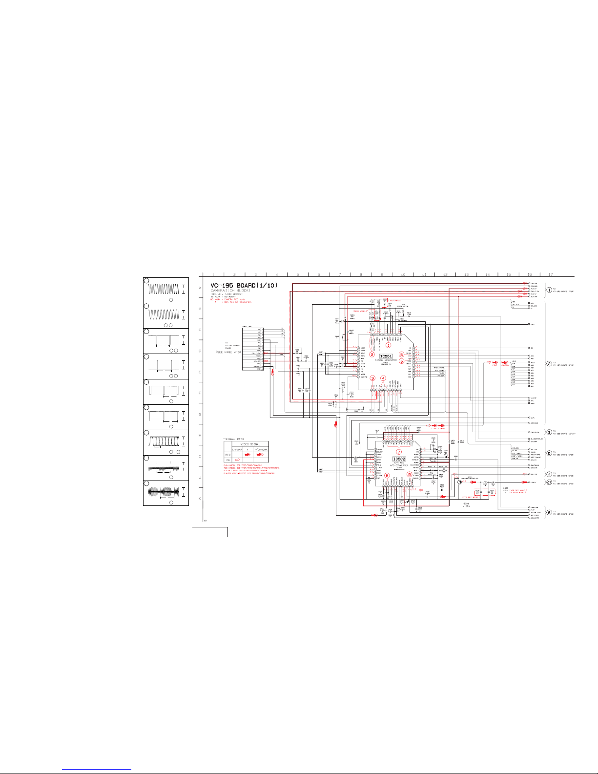
CCD-TR57/TR67/TR87/TR413PK/TR414PK/TR917/TR940/TR940PK
4-18 4-19 4-20
VC-195 BOARD (1/10)
1
2
3
4
5
6
7
8
9
2.3Vp-p
CAMERA REC
2.3Vp-p
IC501
CAMERA REC
11 12
,
H
7Vp-p
IC501
25
CAMERA REC
26
,
H
7Vp-p
IC501
28
CAMERA REC
31
,
H
3Vp-p
IC501
44
CAMERA REC
V
3Vp-p
IC501
45
CAMERA REC
3.2Vp-p
IC502
2 10
CAMERA REC
H
1.3Vp-p
IC502
26
CAMERA REC
H
0.4Vp-p
IC502
36
PB
—
0.14usec
IC501
5
28.636 MHz
14.32 MHz
CAMERA (1)
VC-195 (1/10)
• For schematic diagrams.
• Refer to page 4–13 for Printed Wiring Board.
CCD-TR57/TR67/TR87/TR413PK/TR414PK/TR917/TR940/TR940PK
CCD-TR57/TR67/TR87/TR413PK/TR414PK/TR917/TR940/TR940PK
4-21 4-22
4-23
4-24
CAMERA (2)
VC-195 (2/10)
• For schematic diagrams.
• Refer to page 4–13 for Printed Wiring Board.
CCD-TR57/TR67/TR87/TR413PK/TR414PK/TR917/TR940/TR940PK
CCD-TR57/TR67/TR87/TR413PK/TR414PK/TR917/TR940/TR940PK
4-25
4-26 4-27
4-28
Y/C PROCESSOR
VC-195 (3/10)
VC-195 BOARD (3/10)
10 20
21
22
23
24
25
26
27
28
29
11
12
13
14
15
16
17
18
19
H
0.34Vp-p
IC202
3
CAMERA REC
H
0.84Vp-p
IC202
6
CAMERA REC
4V
3Vp-p
IC202
71
CAMERA REC
2V
3Vp-p
IC202
72
CAMERA REC
V
3Vp-p
IC202
81
CAMERA REC
3.2Vp-p
IC201
8
CAMERA REC
H
3Vp-p
IC202
80
PB
H
0.5Vp-p
IC202
13
CAMERA REC
H
0.4Vp-p
IC202
16
CAMERA REC
H
0.18Vp-p
IC202
23
CAMERA REC
H
0.18Vp-p
IC202
26
CAMERA REC
H
0.9Vp-p
IC202
33
CAMERA REC
V
0.4Vp-p
IC202
40
PB
V
3Vp-p
IC202
60
CAMERA REC
H
3Vp-p
IC202
61
CAMERA REC
IC202
66
3.58 MHz
3.1Vp-p
CAMERA REC
7.16 MHz
V
3Vp-p
IC201
19
CAMERA REC
H
3Vp-p
IC201
20
CAMERA REC
0.14usec
3.5Vp-p
IC204
12 15
CAMERA REC
—
3.5Vp-p
IC204
23 30
CAMERA REC
—
0.14usec
• For schematic diagrams.
• Refer to page 4–13 for Printed Wiring Board.
 Loading...