

Siemens TLE5226G Datasheet
TLE 5226 G
Smart Quad Channel Low-Side Switch
Features Product Summary
• Low ON-resistance 2 x 0.2 Ω , 2 x 0.35 Ω (typ.)
• Power - SO 20 - Package with integrated
cooling area
• Overload shutdown
Supply voltage V
Drain source voltage V
On resistance R
• Selective thermal shutdown
• Status monitoring
Output current I
• Overvoltage protection
• Shorted circuit protection
• Standby mode with low current consumption
• µC compatible input
• Electostatic discharge (ESD) protection
Application
• All kinds of resistive and inductive loads (relays,electromagnetic valves)
• µC compatible power switch for 12 and 24 V applications
• Solenoid control switch in automotive and industrial control systems
General description
Quad channel Low-Side-Switch (2x5A/2x3A) in Smart Power Technology (SPT) with four seperate inputs and four open drain DMOS output stages. The T LE 5226 is fully protected by embedded pr otection functions and designed for automotive and industrial applications.
4.8 - 32 V
S
DS(AZ)max
ON(typ) 1,2
R
ON(typ) 3,4
D 1,2
I
D 3,4
60 V
0.2 Ω
0.35 Ω
2 x 5 A
2 x 3 A
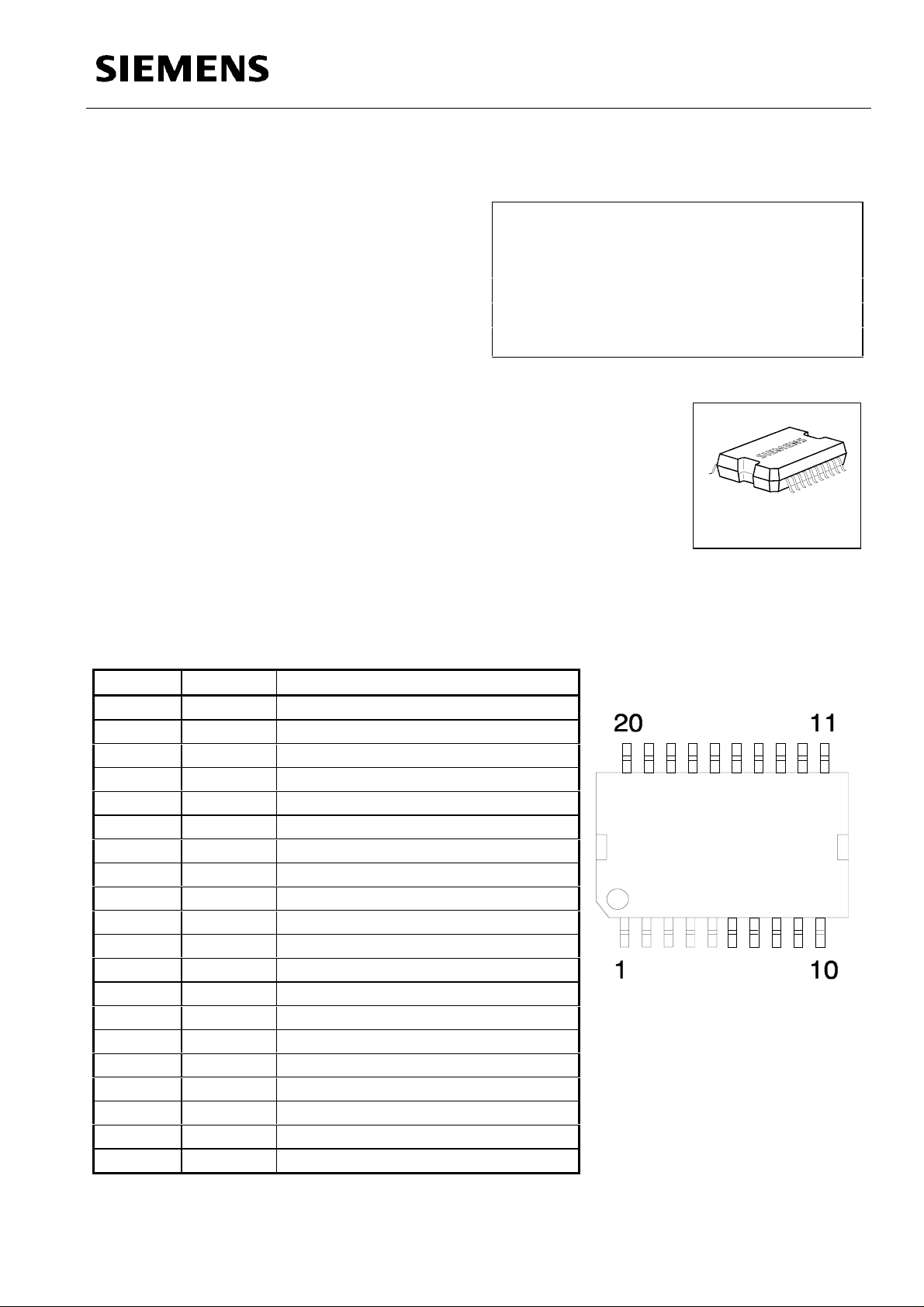
P-DSO-20-10
Pin Description Pin Configuration (Top view)
Pin Symbol Function
1 GND Ground
2 OUT1 Power Output channel 1
3 ST1 Status Output channel 1
4 IN4 Control Input channel 4
5 VS Supply Voltage
6 STBY Standby
7 IN3 Control Input channel 3
8 ST2 Status Output channel 2
9 OUT2 Power Output channel 2
10 GND Ground
11 GND Ground
12 OUT3 Power Output channel 3
13 ST3 Status Output channel 3
14 IN2 Control Input channel 2
P - DSO - 20 - 10
15 GND Ground Logic
16 ENA Enable Input for all four channels
17 IN1 Control Input channel 1
18 ST4 Status Output channel 4
19 OUT4 Power Output channel 4
20 GND Ground
Semiconductor Group Page 1998-02-04
1
VS
TLE 5226 G
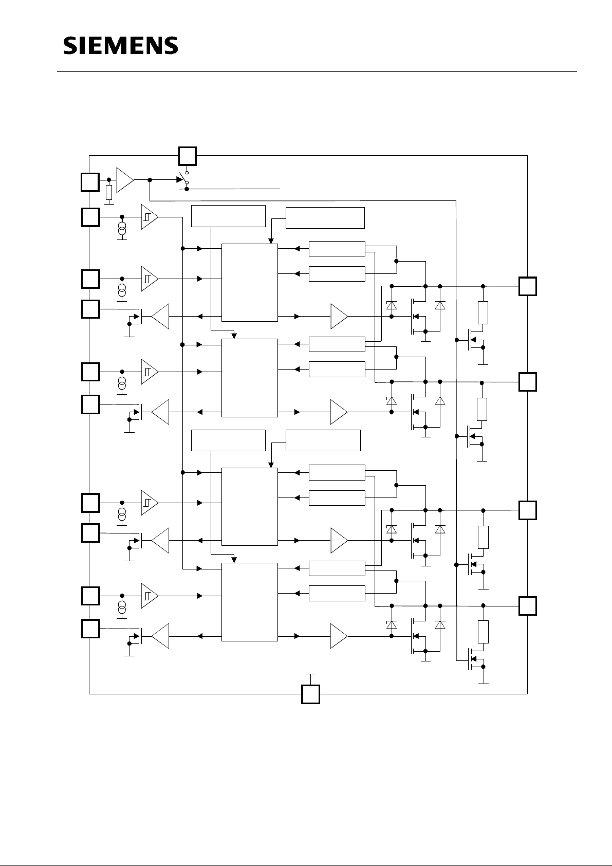
Block Diagram
STBY
ENA
IN1
ST1
IN4
ST4
internal supply
Overtemperature
Channel 4
LOGIC
LOGIC
Overtemperature
Channel 3
Overtemperature
Channel 1
Open Load
Overload
OUT1
RPD
Open Load
Overload
OUT4
RPD
Overtemperature
Channel 2
Open Load
IN2
ST2
IN3
ST3
LOGIC
LOGIC
Overload
OUT2
RPD
Open Load
Overload
OUT3
RPD
GND
Semiconductor Group Page 1998-02-04
2
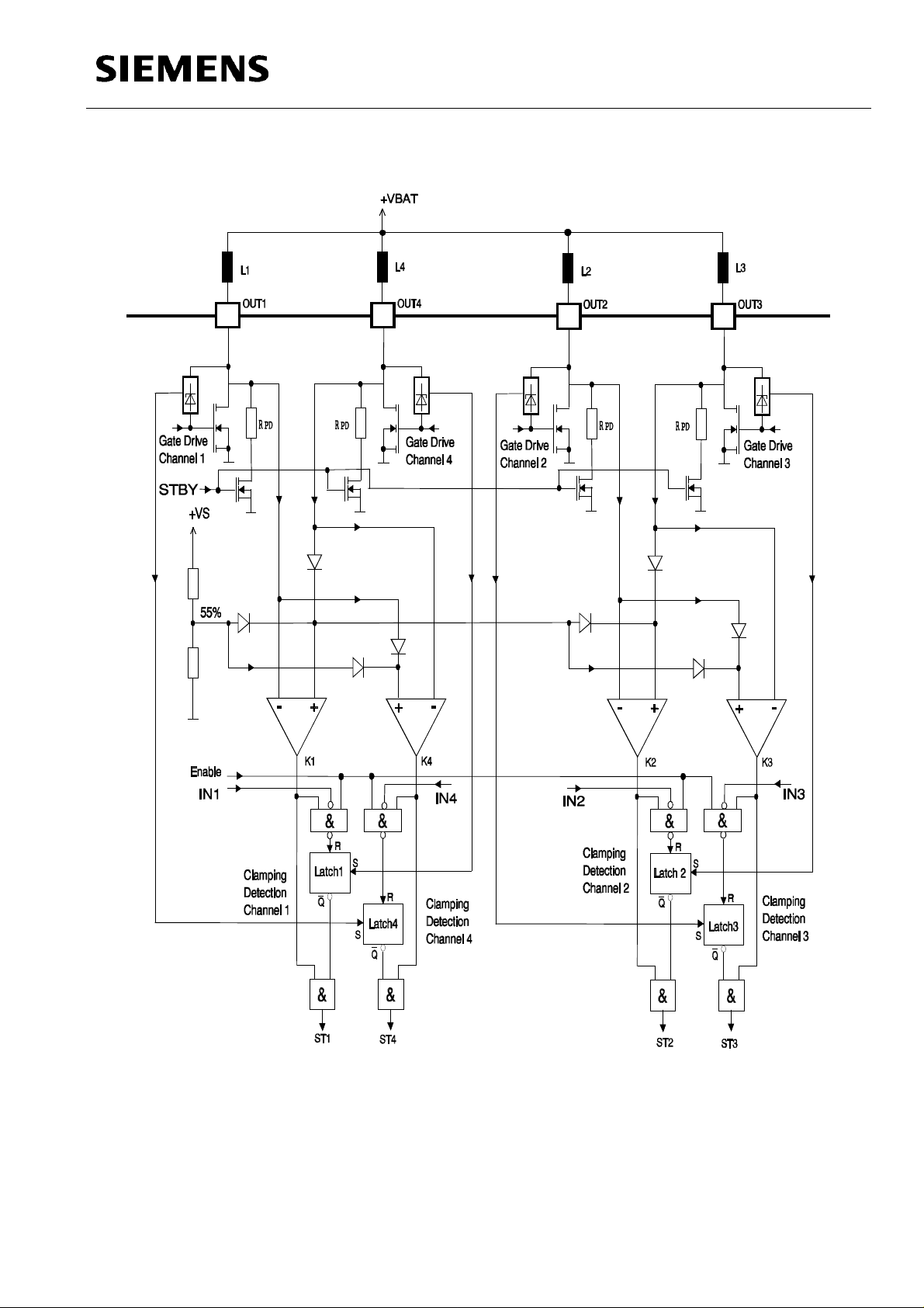
Block Diagram of Open Load Detection
TLE 5226 G
Semiconductor Group Page 1998-02-04
3
TLE 5226 G
Maximum Ratings for Tj = – 40°C to 150°C
Parameter Symbol Values Unit
Supply voltage
Supply voltage operational range
Continuous drain source voltage (OUT1...OUT4)
Input voltage IN1 to IN4, ENA
Input voltage STBY
Status output voltage
Operating temperature range
Storage temperature range
Output current per channel
Output current at reversal supply
Status output current
Inductive load switch off dissipation energy Tj = 25°C
Thermal resistance
junction - case
junction - ambient @ min. footprint
junction - ambient @ 6 cm
2
cooling area
V
S
V
S
V
DS
V
IN
V
STBY
V
ST
T
j
T
stg
I
D(lim)
I
D 1,2
I
D 3,4
I
ST
E
AS
R
thJC
R
thJA
-0.3 ... + 40 V
+ 4.8 ... + 32 V
40 V
,
V
ENA
- 0.3 ... + 6 V
- 0.3 ... + 40
- 0.3 ... + 32 V
- 40 ... + 150
°C
- 55 ... + 150
self limited A
- 4
- 2
- 5 ... + 5 mA
50 mJ
K/W
4.5
50
40
A
Test board for
6 cm2 cooling area min. footprint
Semiconductor Group Page 1998-02-04
4
 Loading...