

Smart Quad Channel Low-Side Switch TLE 5216 G
SPT-IC
Features
• Overload protection
• Short circuit protection
• Cascadeable serial diagnostic interface
• Overvoltage protection
• µC compatible input
• Electrostatic discharge (ESD) protection
P-DSO-20-10
Type Ordering Code Package
▼
TLE 5216 G Q67006-A9206 P-DSO-20-10
▼ New Type
Application
• All kinds of resistive and inductive loads (relays, electromagnetic valves)
• µC compatible power switch for 12 V applications
• Solenoid control switch in automotive and industrial control systems
Semiconductor Group 1 1998-06-22
TLE 5216 G
General Description
Quad channel Low-Side Switch in Smart Power Technology (SPT) with four separate
LOW active inputs and four open drain DMOS output stages. The TLE 5216G is
protected by embedded protection functions and designed for automotive and industrial
applications.
Product Summary
Parameter Symbol Values Unit
Supply voltage
Drain source clamping voltage
(OUT1 - OUT4)
ON resistance
Output current
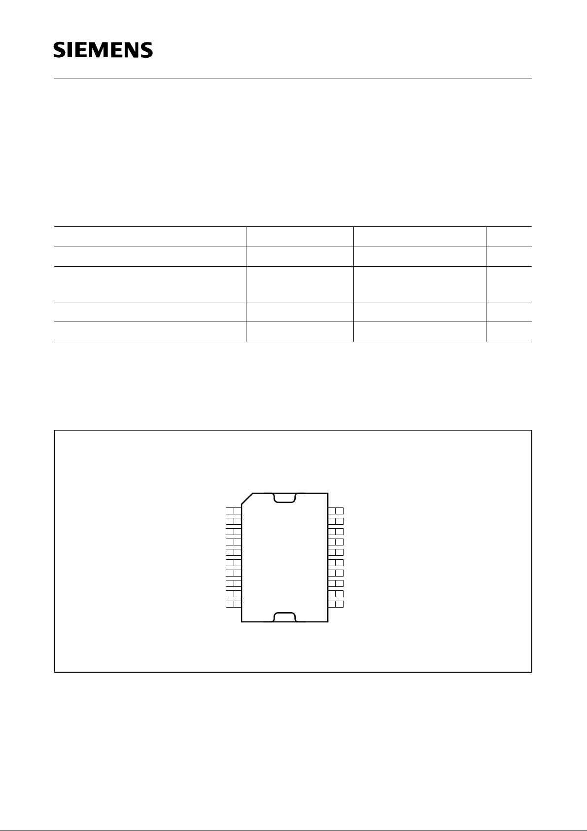
Pin Configuration
(top view)
GND
N.C.
IN1
IN2
OUT1
V
SEROUT SERIN
GND
V
V
R
I
D
P-DSO-20-10
1
2
3
4
5
6
S
7
8
9
10
S
DS(AZ)max
ON(typ)
20
19
18
17
16
15
14
13
12CLK
11
6 … 30 V
75 V
0.35 Ω
4 × 2A
GND
N.C.
IN4
IN3
OUT4
RESET
OUT3OUT2
CS
GND
AEP01617
Figure 1
Semiconductor Group 2 1998-06-22
TLE 5216 G
Pin Definitions and Functions
Pin No. Symbol Function
3 IN1 Input switch 1; active LOW; internal pull-up
4 IN2 Input switch 2; active LOW; internal pull-up
5 OUT1 Output switch 1; overload and shorted load protected
6
V
S
Supply voltage
7 OUT2 Output switch 2; overload and shorted load protected
8 SEROUT Data-out of serial diagnostic interface;
open drain
9 CLK Clock for serial diagnostic interface
1, 10, 11, 20 GND Ground
12 CS Chip select for serial diagnostic interface; internal pull-up
13 SERIN Data-in of serial diagnostic interface; internal pull-up
14 OUT3 Output switch 3; overload and shorted load protected
15 RESET Reset; active LOW; shuts down all outputs and resets
the error flags
16 OUT4 Output switch 4;
overload and shorted load protected
17 IN3 Input switch 3; active LOW; internal pull-up
18 IN4 Input switch 4; active LOW; internal pull-up
2, 19 N.C. Not connected
Semiconductor Group 3 1998-06-22
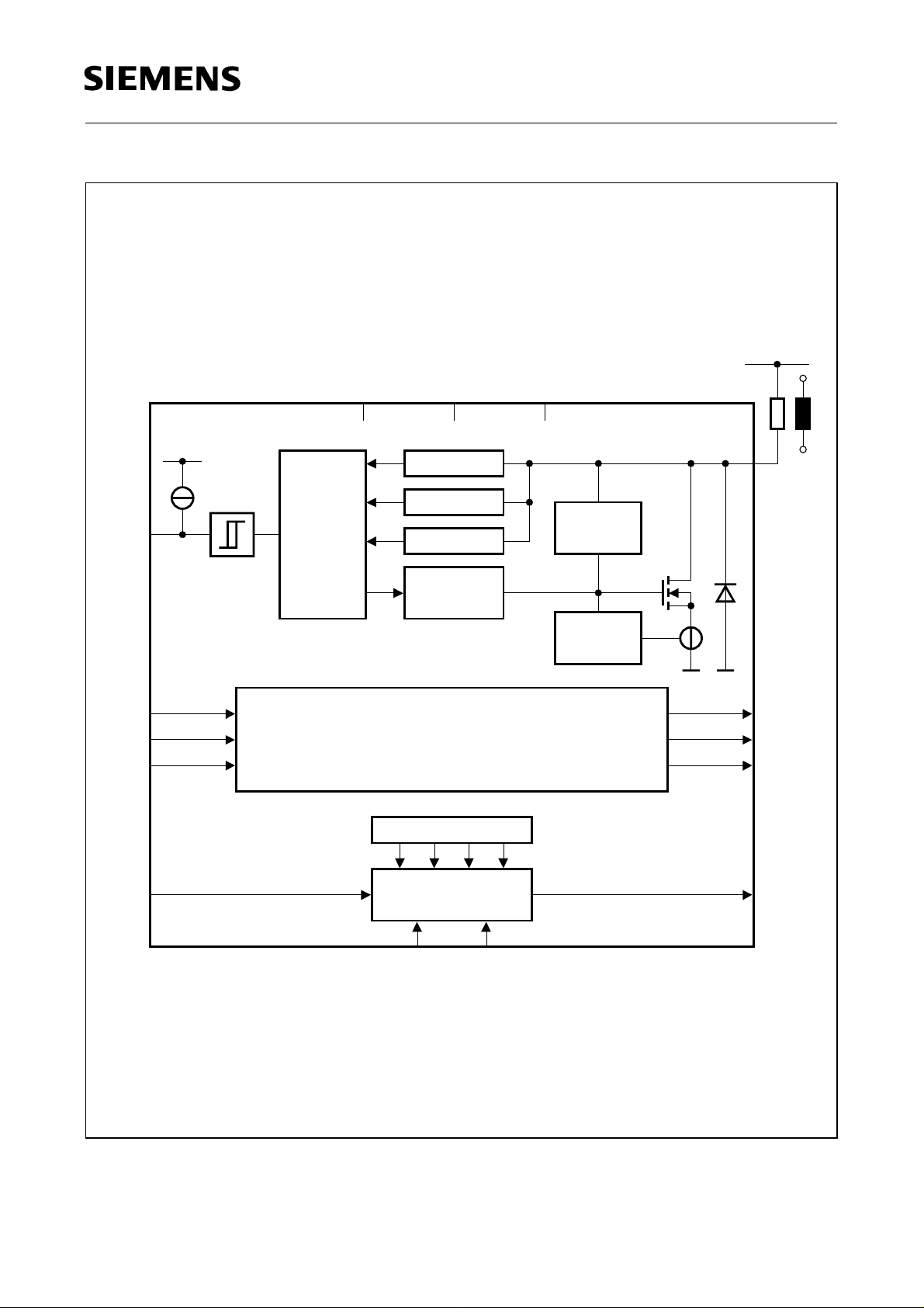
TLE 5216 G
V
BB
V
S
GNDRESET
TLE 5216 G
V
Internal
Overload
OUT1
Open Load
Clamp
Regulator
IN1
Logic
Channel 1
Short to GND
dv/dt Circuit
Current
Limit
IN2
IN3
IN4
Logic, Protection- and Power-Circuit of Channel 2-4
(equivalent to Channel 1)
OUT2
OUT3
OUT4
Logic Channel 1-4
SERIN SEROUT
Serial Diagnostic
Interface
CS CLK
AES02013
Figure 2
Block Diagram
Semiconductor Group 4 1998-06-22

TLE 5216 G
Application Description
This IC is specially designed to drive inductive loads up to 2 A nominal current (valves,
relays, etc.). Integrated clamp-diodes limit the output voltage when inductive loads are
turned off.
For the detection of errors at the load there is a serial diagnostic interface, which
monitors the following errors for every output separately:
– open load in inactive mode
– shorted output (shorted to ground) in inactive mode
– overload or shorted load in active mode
Circuit Description
The block diagram shows the four independent power drivers with the referring logic
block and the serial diagnostic interface which stores and transfers the diagnostic
signals to the external circuit. Each power switch connects a high side load to ground
when a LOW signal applies at the inputs. To protect the IC against short circuit and over
load each output is provided with a current limitation and a delayed overload shutdown.
The slew rate of the switching process is limited internally.
The integrated clamp diodes limit the voltage at the output to
V
, when inductive
DS(AZ)
loads are switched off. The maximum power dissipation, which is given from the static
and dynamic thermal resistance, limits the allowable inductive energy. A diode in parallel
to every output clamps negative voltage.
All outputs, preferably the outputs 1 and 2 and the outputs 3 and 4 may be used in
parallel (no addition of max. freewheeling energy).
A curve of the output voltage is shown in figure 6.
The diagnostic block monitors the voltages across the power switch. If in active mode
(LOW level input) there is a higher voltage than
V
for a time longer than t
DS(OV)
VDS(OV)
, the
diagnostic block will show an overload in the error register and the affected power switch
will be shut off. The switch can only be reactivated if the corresponding input is switched
off and then on again.
In inactive mode (HIGH level at input) open load or shorted output (shorted load to
ground) is detected and signalled to the serial diagnostic interface. If the voltage across
the power switch is lower than
identified. If the voltage is even lower than
V
DS(OL)
for the time t
V
for the time t
DS(SH)
VDS(OL)
(min. 50 µs) open load is
VDS(SH)
(min. 30 µs)
"shorted to ground" is detected. An internal voltage divider will pull the output to the
voltage
V
if there is an open load.
DS
A new error on the same output stage will over-write the old error report. The protocol of
the serial diagnostic interface includes independent error reports for each output driver.
As soon as an error is latched into the error register the serial data output (SEROUT) of
the interface will go LOW (while CS is still HIGH). If the chip select gets a LOW signal
Semiconductor Group 5 1998-06-22
TLE 5216 G
(CS = L), all error reports can be shifted out serially. The rising edge of the CS will reset
all error registers. The function of the serial diagnostic interface is shown in figure 7.
The data input (SERIN) allows several TLE 5216 G or other serial diagnostic interfaces
to be cascaded.
A LOW signal on the reset pin (RESET) or a supply voltage lower than the operating
range (4.5 V) will erase the error register and disable all four power switches.
Absolute Maximum Ratings
T
= – 40 °C to 150 °C
j
Parameter Symbol Values Unit
Supply voltage
Input voltages IN1 … IN4, SERIN, CLK, CS, RESET
Status output voltage Data OUT (SEROUT)
Operating temperature range
Storage temperature range
Output current per channel
Ground pin current
T
= 25 °C
j
T
= 125 °C
j
T
= 25 °C
j
T
= 125 °C
j
V
S
V
IN
V
SEROUT
T
j
T
Stg
I
D(AZ)
I
D(AZ)
I
GND
I
GND
– 2…40 V
– 0.3 … 7 V
– 0.3 … 10 V
– 40 … 150 °C
– 50 … 150 °C
– 3.8 … 3.8
– 2.95 … 2.95AA
– 10 … 10
– 8…8
A
A
Thermal resistance (junction-case static)
See diagrams P-DSO-20-10
R
thJC
5 K/W
Transient thermal impendance
t
= 100 µs; square pulse
p
t
= 100 µs; triangle pulse
p
Z
thJC
Z
thJC
0.5
0.2
K/W
K/W
Note: Maximum ratings are absolute ratings; exceeding only one of these values may
cause irreversible damage to the integrated circuit.
Semiconductor Group 6 1998-06-22
 Loading...