Programmable
SAE 800
Single-/Dual-/Triple- Tone Gong
Preliminary Data Bipolar IC
Features
● Supply voltage range 2.8 V to 18 V
● Few external components (no electrolytic capacitor)
● 1 tone, 2 tones, 3 tones programmable
● Loudness control
● Typical standby current 1 µA
● Constant current output stage (no oscillation)
● High-efficiency power stage
● Short-circuit protection
● Thermal shutdown
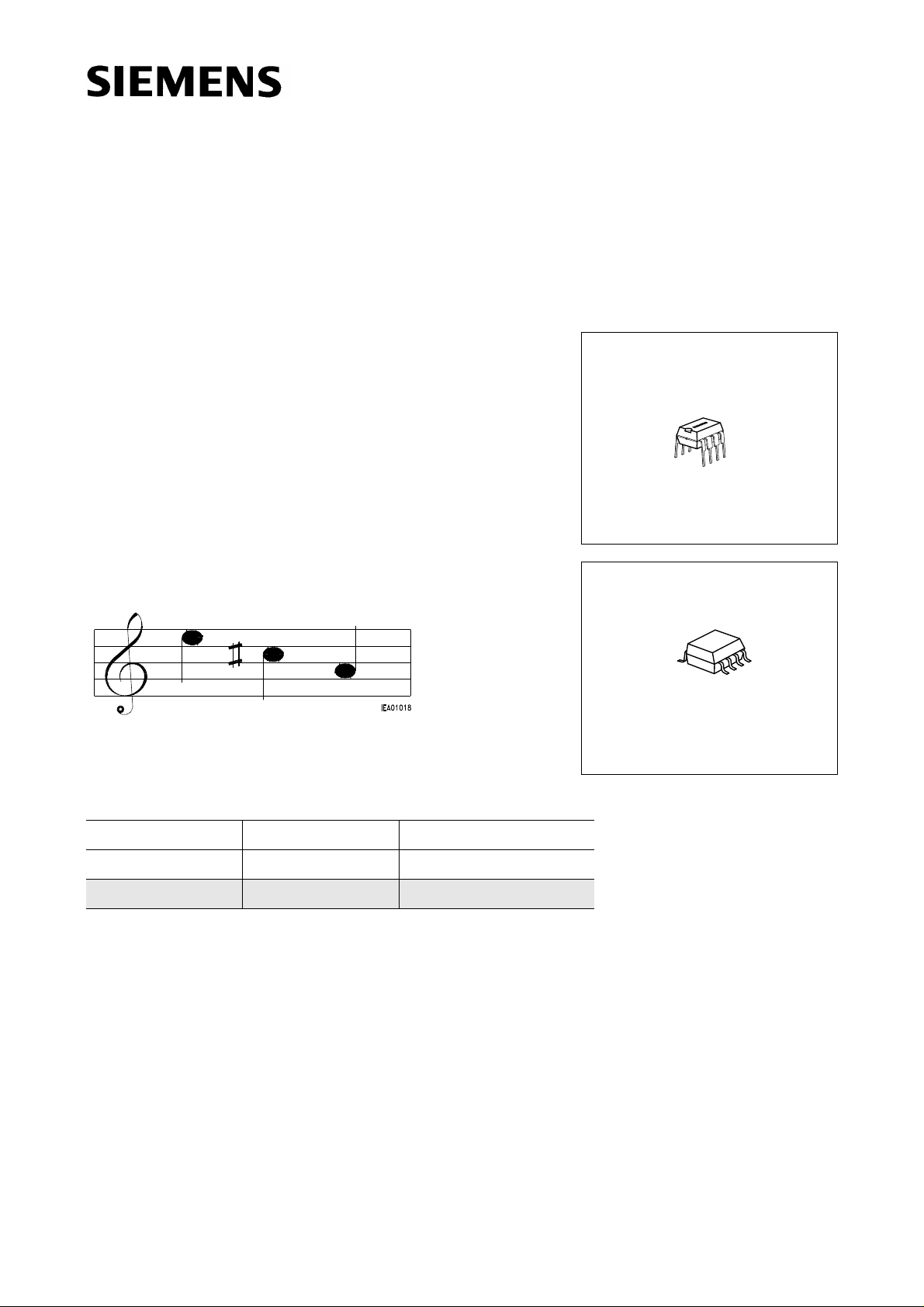
P-DIP-8-4
P-DSO-8-1
Type Ordering Code Package
▼ SAE 800 Q67000-A8339 P-DIP-8-4
▼
SAE 800 G Q67000-A8340 P-DSO-8-1 (SMD)
▼ New type
Functional Description
The SAE 800 is a single-tone, dual-tone or triple-tone gong IC designed for a very wide supply
voltage range. If the oscillator is set to f0 = 13.2 kHz for example, the IC will issue in triple-tone-
mode the minor and major third e2 – C sharp – a, corresponding to 660 Hz – 550 Hz – 440 Hz, in
dual-tone-mode the minor third e2 – C sharp, and in single-tone-mode the tone e2 (derived from
the fundamental frequency f0; f1 = f0 / 20, f2 = f0 / 24, f3 = f0 / 30).
When it is not triggered, the IC is in a standby state and only draws a few µA. It comes in a compact
P-DIP-8-1 or P-DSO-8-1 (SMD) package and only requires a few external components.
Semiconductor Group 1 09.94
SAE 800 SAE 800 G
SAE 800
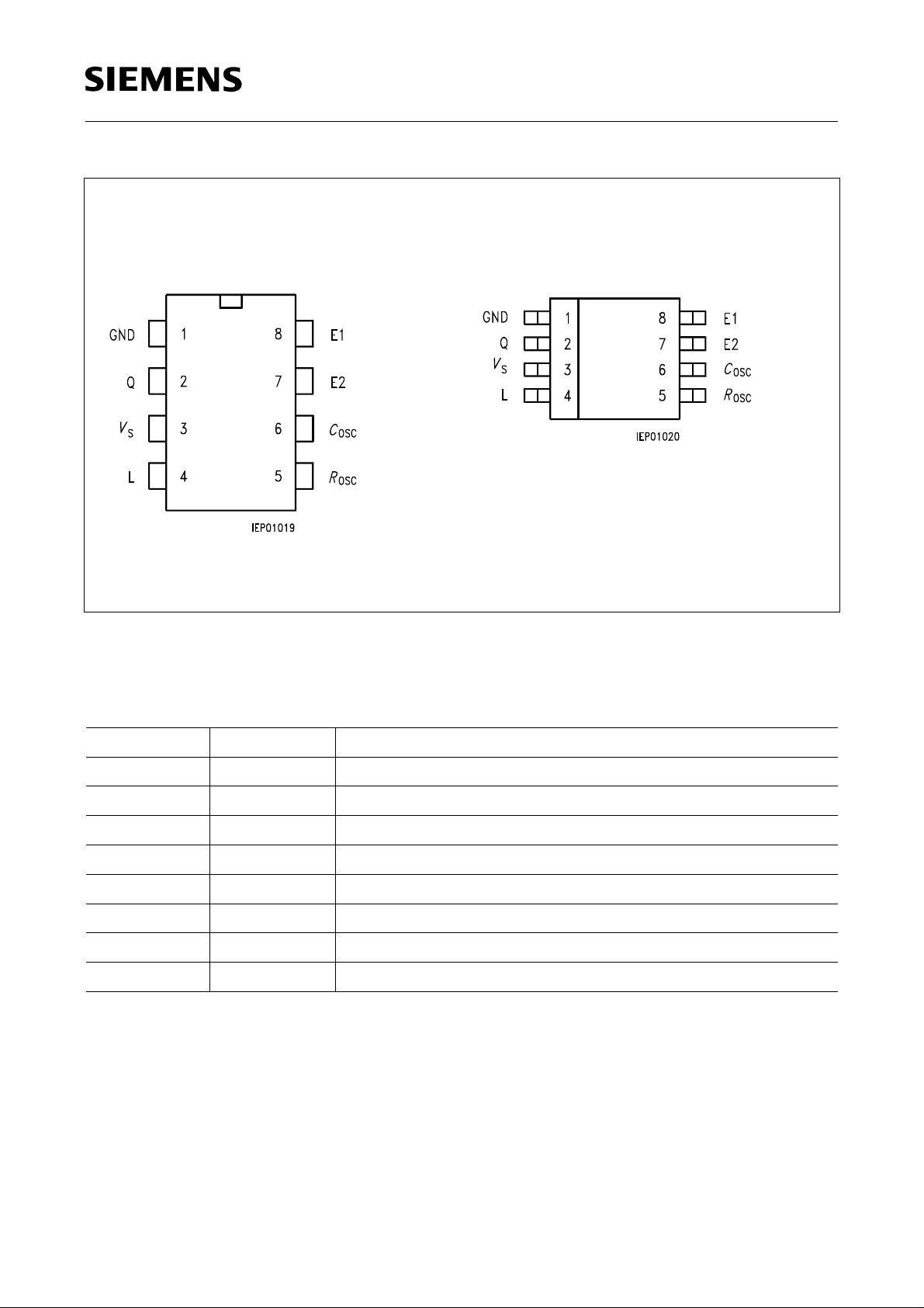
Pin Configuration
(top view)
Pin Definitions and Functions
Pin Symbol Function
1 GND Ground
2 Q Output
3
V
S
Supply Voltage
4 L Loudness Control
5
6
R
C
OSC
OSC
Oscillator Resistor
Oscillator Capacitor
7 E2 Trigger 2 (dual tone)
8 E1 Trigger 1 (single tone)
Functional Description (cont’d)
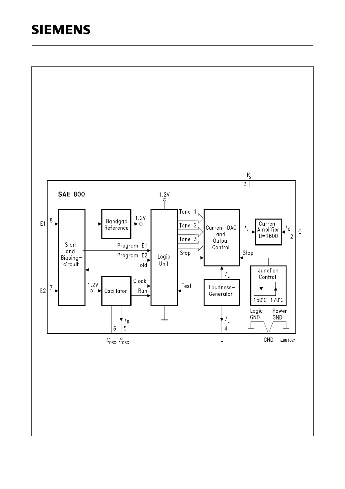
An RC combination is needed to generate the fundamental frequency (pin
R
, C
OSC
). The volume
OSC
can be adjusted with another resistor (pin L). The loudspeaker must be connected directly between
the output Q and the power supply VS. The current-sink principle combined with an integrated
thermal shutdown (with hysteresis) makes the IC overload-protected and shortcircuit-protected.
There are two trigger pins (E1, E2) for setting single-tone, dual-tone or triple-tone mode.
Semiconductor Group 2
SAE 800
Block Diagram
Semiconductor Group 3
SAE 800
Circuit Description
Trigger
Positive pulses on inputs E1 and/or E2 trigger the IC. The hold feedback in the logic has a delay of
several milliseconds. After this delay has elapsed, the tone sequence is started. This prevents
parasitic spikes from producing any effect on the trigger pins.
The following table shows the trigger options:
E1 E2 Mode Issued Sequence
Triggered Triggered Triple-tone Minor and major third
Grounded/open Triggered Dual-tone Minor third
Triggered Grounded/open Single-tone 1st tone of minor third
Oscillator
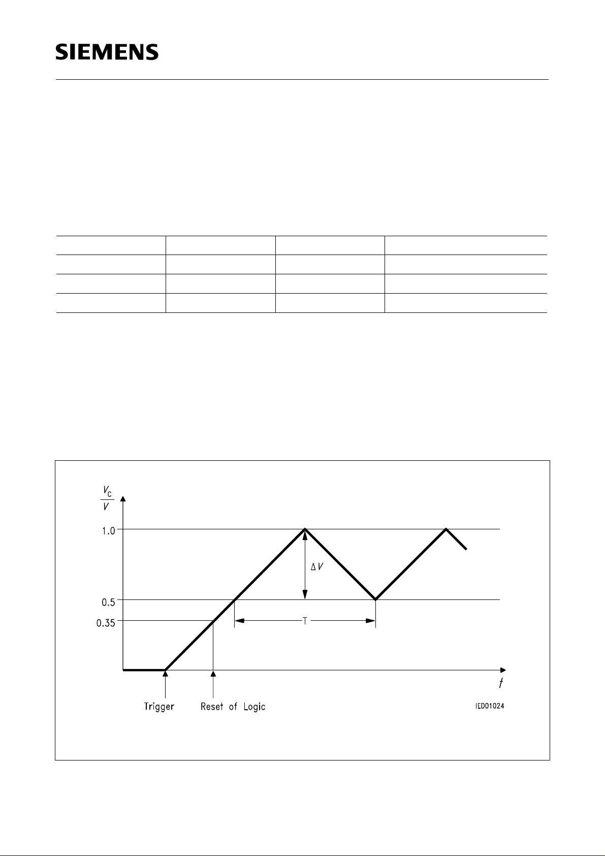
This is a precision triangle oscillator with an external time constant (R x C). CapacitorCC on pin C
OSC
is charged by constant current to 1 V and then discharged to 0.5 V. The constant current is obtained
on pin R
When the voltage on C
with an external resistor RR to ground.
OSC
is building up, the logic is reset at 350 mV. This always ensures that a
OSC
complete tone sequence is issued. If the oscillator pin is short-circuited to GND during operation,
the sequence is repeated.
The following applies:
Voltages on Pin C
OSC
∆V
x CC = IC x T/2 with IC = VR/2RR = 1.2 V/2R
C
f
= 5/8 x 1/(RR x CC)
0
Semiconductor Group 4
R
SAE 800
Logic
The logic unit contains the complete sequence control. The oscillator produces the power-on reset
and the clock frequency. Single-tone, dual-tone or triple-tone operation is programmed on inputs
E1 and E2. The 4-bit digital/analog converters are driven in parallel. In the event of oscillator
disturbance, and after the sequence, the dominant stop output is set. By applying current to pin L,
the sequence can be shortened by a factor of 30 for test purposes.
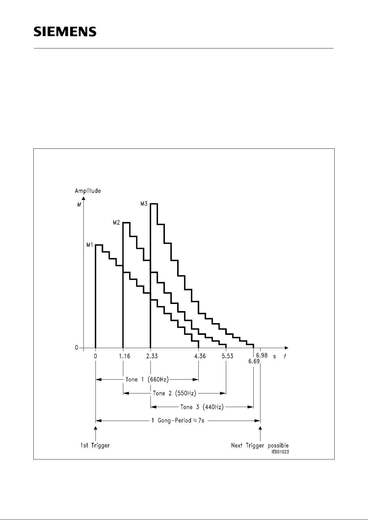
The following figure shows the envelope of the triple-tone sequence:
Envelope of maximum amplitudes of three
superimposed tones on Q (time scale for
f
= 13.2 kHz)
OSC
Ratio of maximum amplitudes
M3 : M2 : M1 = 1 : 0.89 : 0.67
Envelope of the Triple-Tone Sequence
Semiconductor Group 5

SAE 800
Digital / Analog Converter, Loudness and Junction Control
The DAC converts the 4-bit words from the logic into the appropriate staircase currents with the
particular tone frequency. The sum current IIdrives the following current amplifier. The loudness
generator produces the DAC reference current IL for all three tones. This requires connecting an
external resistor to ground. The chip temperature is monitored by the junction control. At
temperatures of more then approx. 170 ˚C the stop input will switch the output currentII to zero. The
output current is enabled again once the chip has cooled down to approx. 150 ˚C.
Current Amplifier
The current amplifier with a gain of 1600 boosts the current II from approx. 470 µA maximum to
approx. 750 mA maximum. The output stage consists of an NPN transistor with its emitter on power
GND and collector on pin Q.
The current control insures that the output stage only conducts defined currents. In conjunction with
the integrated thermal shutdown, this makes the configuration shortcircuit-protected within wide
limits. Because of the absence of feedback the circuit is also extremely stable and therefore
uncritical in applications. Resistor RL on pin L sets the output voltage swing. This assumes that the
resistive component of the loudspeaker impedance RQ responds similarly as the resistance RL.
The output amplitude of the current II reaches the maximum I
Imax
(only 3 tone mode), so RL has to be scaled for this point.
The following applies:
I
= I
Q
3 x B x (VL / RL) ≈ 0.8 VS / R
x B = (VS – V
Imax
) / RQ≈ 0.8 VS / R
sat
Q
Q
the result is:
R
= RQ x 3 x B x (VL / 0.8 VS) with: B = 1600
L
R
= RQ x K x (VL / 0.8 VS) with: K = 4800
L
≅ 3 x VL / RL at a time t of 2.33 s
Semiconductor Group 6

SAE 800
Application Hints and Application Circuit
1) Loudness Resistor (max. Load Current of 3-Tone Signal with Ensured Ratio of Amplitudes)
0.8 VS / RQ≈ (VL / RL) x K
R
= (VL / 0.8 VS) x RQ x K; K = 4800
L
Example: RQ = 8 Ω; VS = 5 V; VL = 1.2 V
R
= (1.2 / 4) x 8 Ω x 4800 ≈ 12 kΩ
L
2) Oscillator Elements RR, C
f = 5 / 8 x 1 / (R
x CC)
R
C
Example: f = 13.2 kHz; CC = 4.7 nF
R
= 5 / (8 x 13.2 x 4.7) x 106Ω≈ 10 kΩ
R
The following is a typical application circuit
Application Circuit
Semiconductor Group 7

Absolute Maximum Ratings
Parameter Symbol Limit Values Unit
min. max.
SAE 800
Supply voltage V
Input voltage at E1, E2
Current at output Q
Current at input pins E1, E2
Current at pin
R
OSC
Current at pin L
Current at pin C
OSC
Junction temperature
Storage temperature
Operating Range
Supply voltage V
Junction temperature
Oscillator frequency at
Current at pin
R
OSC
C
OSC
Current for test mode at pin L
Current at pin L
Input voltage at E1, E2
Thermal resistance
junction-air (P-DIP-8-4)
junction-air (P-DSO-8-1)
S
V
E1, E2
I
Q
I
E1, E2
I
R
I
L
I
C
T
j
T
stg
S
T
j
f
C
I
R
I
R
I
L
V
E1, E2
R
th JA
R
th JA
– 0.3 24 V
– 5 24 V
– 50
– 2
– 300
– 300
– 200
750
3
200
200
200
mA
mA
µA
µA
µA
– 50 150 ˚C
– 50 150 ˚C
2.8 18 V
– 25 125 ˚C
100 kHz
– 200
90
– 200
– 10
110
– 10
µA
µA
µA
– 4 18 V
100
180
K/W
K/W
Semiconductor Group 8

Characteristics
T
= – 25 to 125˚C; VS = 2.8 to 18 V
j
Parameter Symbol Limit Values Unit Test
min. typ. max.
Condition
Supply Section
SAE 800
Standby current
Quiescent current; pin L open
Output Section
Peak output power (tone 3)
V
= 2.8 V; RQ = 4 Ω; RL = 8.2 kΩ
S
V
= 2.8 V; RQ = 8 Ω; RL = 18 kΩ
S
V
= 5.0 V; RQ = 8 Ω; RL = 10 kΩ
S
V
= 5.0 V; RQ = 16 Ω; RL = 18 kΩ
S
V
= 12 V; RQ = 50 Ω; RL = 33 kΩ
S
Output level differences:
tone 1 to 3
tone 2 to 3
Biasing Section
Voltage at pin
R
; RR = 10 kΩ
OSC
Voltage at pin L; RL = 10 kΩ
Oscillator Section
I
St
I
Qu
P
Q
P
Q
P
Q
P
Q
P
Q
a
13
a
23
V
R
V
L
250
125
450
225
450
– 1
– 1
1
5
330
165
600
300
600
1.2
1.2
10
10
1
1
µA
mA
mW
mW
mW
mW
mW
dB
dB
V
V
A
1)
A
2)
A
Amplitude
Frequency
C
= 4.7 nF
C
R
= 10 kΩ;
R
Oscill. drift vs. temperature
Oscill. drift vs. supply voltage
∆V
f
0
D
D
C
T
V
– 3
Input Section
Triggering voltage at E1, E2
Triggering current at E1, E2
Noise voltage immunity at E1, E2
Triggering delay at f0 = 13.2 kHz
1) a13 = 20 x log (M1 / (0.67 x M3))
2) a23 = 20 x log (M2 / (0.89 x M3))
V
E1 , E2
I
E1 , E2
V
E1 , E2
t
dT
1.6
100
2
Semiconductor Group 9
0.5
13.2
1
+ 3
0.3
10
V
kHz
10-4/K
10-3/K
V
µA
V
ms

SAE 800
Output Peak Voltage VQ versus
Loudness-Current I
L
Max. Output Power PQ versus
Loudness-Current I
L
Power Dissipation Pv of Output Stage
versus Loudness-Current I
L
Peak Current IQ versus Loudness-Current I
L
*) Note that IQ = f (IL) varies between 0 and K ⋅ IL during tone sequence. Thereby the maximum of the power
dissipation during the tone sequence is the maximum of P
(in diagram) between IL = 0 and chosen IL = VL/RL.
v
Semiconductor Group 10

SAE 800
Output Peak Voltage VQ versus
Loudness-Current I
L
Max. Output Power PQ versus
Loudness-Current I
L
Power Dissipation
P
of Output Stage
v
versus Loudness-Current I
Peak Current IQ versus Loudness-Current I
L
L
*) Note that IQ = f (IL) varies between 0 and K ⋅ IL during tone sequence. Thereby the maximum of the power
dissipation during the tone sequence is the maximum of P
(in diagram) between IL = 0 and chosen IL = VL/RL.
v
Semiconductor Group 11

SAE 800
Circuit for SAE 800 Application in Home Chime Installation Utilizing AC and DC Triggering
for 1, 2 or 3 Tone Chime; Adjustable Volume
PCB layout information: Because of the peak currents at VS, Q and GND the lines should be
designed in a flatspread way or as star pattern.
Semiconductor Group 12

SAE 800
Circuit for SAE 800 Application in Home Chime Installation for Operation without Battery
Semiconductor Group 13

Package Outlines
Plastic-Package, P-DIP-8-4
(Plastic Dual In-Line Package)
SAE 800
Plastic-Package, P-DSO-8-1 (SMD)
(Plastic Dual Small Outline)
GPD05583
GPS05121
SMD = Surface Mounted Device Dimensions in mm
Semiconductor Group 14
 Loading...