

Siemens HYB3164405J-50, HYB3164405J-60, HYB3164405T-50, HYB3164405T-60, HYB3164405TL-50 Datasheet
...
16M x 4-Bit Dynamic RAM
(4k & 8k Refresh, EDO-version)
HYB 3164405J/T(L) -50/-60
HYB 3165405J/T(L) -50/-60
Preliminary Information
• 16 777 216 words by 4-bit organization
• 0 to 70 ˚C operating temperature
• Fast access and cycle time
RAS access time:
50 ns (-50 version)
60 ns (-60 version)
Cycle time:
84 ns (-50 version)
104 ns (-60 version)
CAS access time:
13 ns ( -50 version)
15 ns ( -60 version)
• Hyper page mode (EDO) cycle time
20 ns (-50 version)
25 ns (-60 version)
• Single + 3.3 V (± 0.3V) power supply
• Low power dissipation
max. 396 active mW ( HYB 3164405J/T(L)-50)
max. 360 active mW ( HYB 3164405J/T(L)-60)
max. 504 active mW ( HYB 3165405J/T(L)-50)
max. 432 active mW ( HYB 3165405J/T(L)-60)
7.2 mW standby (TTL)
720 W standby (MOS)
14.4 mW Self Refresh (L-version only)
• Read, write, read-modify-write, CAS-before-RAS refresh (CBR),
RAS-only refresh, hidden refresh and self refresh modes
• Hyper page mode (EDO) capability
• 8192 refresh cycles/128 ms , 13 R/ 11C addresses (HYB 3164405J/T(L))
• 4096 refresh cycles/ 64 ms , 12 R/ 12C addresses (HYB 3165405J/T(L))
• Plastic Package:
P-SOJ-34-1 500 mil HYB 3164(5)400J
P-TSOPII-34-1 500 mil HYB 3164(5)400T
Semiconductor Group 89
HYB3164(5)405J/T(L)-50/-60
16M x 4-DRAM
This HYB3164(5)405 is a 64 MBit dynamic RAM organized 16 777 216 by 4 bits. The device is
fabricated in SIEMENS/IBM most advanced first generation 64Mbit CMOS silicon gate process
technology. The circuit and process design allow this device to achieve high performance and low
power dissipation. The HYB3164(5)405 operates with a single 3.3 +/-0.3V power supply and
interfaces with either LVTTL or LVCMOS levels. Multiplexed address inputs permit the HYB
3164(5)400J/T to be packaged in a 500mil wide SOJ-34 or TSOP-34 plastic package. These
packages provide high system bit densities and are compatible with commonly used automatic
testing and insertion equipment.The HYB3164(5)405TL parts have a very low power „sleep mode“
supported by Self Refresh.
Ordering Information
Type Ordering
Code
HYB 3164405J-50 on request P-SOJ-34-1 500 mil DRAM (access time 50 ns)
HYB 3164405J-60 on request P-SOJ-34-1 500 mil DRAM (access time 60 ns)
HYB 3164405T-50 on request P-TSOPII-34-1 500 mil DRAM (access time 50 ns)
HYB 3164405T-60 on request P-TSOPII-34-1 500 mil DRAM (access time 60 ns)
HYB 3164405TL-50 on request P-TSOPII-34-1 500 mil DRAM (access time 50 ns)
HYB 3164405TL-60 on request P-TSOPII-34-1 500 mil DRAM (access time 60 ns)
HYB 3165405J-50 on request P-SOJ-34-1 500 mil DRAM (access time 50 ns)
HYB 3165405J-60 on request P-SOJ-34-1 500 mil DRAM (access time 60 ns)
HYB 3165405T-50 on request P-TSOPII-34-1 500 mil DRAM (access time 50 ns)
HYB 3165405T-60 on request P-TSOPII-34-1 500 mil DRAM (access time 60 ns)
HYB 3165405TL-50 on request P-TSOPII-34-1 500 mil DRAM (access time 50 ns)
HYB 3165405TL-60 on request P-TSOPII-34-1 500 mil DRAM (access time 60 ns)
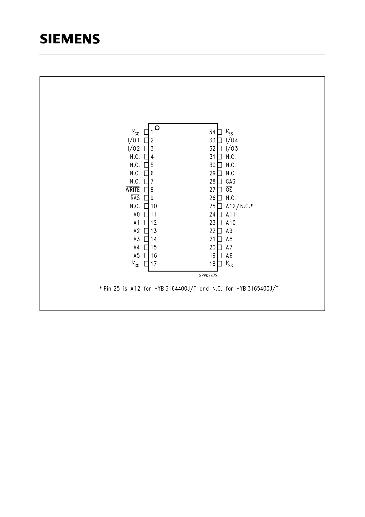
Pin Names
A0-A12 Address Inputs for HYB 3164405J/T(L)
Package Descriptions
A0-A11 Address Inputs for HYB 3165405J/T(L)
RAS Row Address Strobe
OE Output Enable
I/O1-I/O4 Data Input/Output
CAS Column Address Strobe
WRITE Read/Write Input
Vcc Power Supply ( + 3.3V)
Vss Ground
Semiconductor Group 90
P-SOJ-34-1 (500 mil)
P-TSOPII-34-1 (500 mil)
HYB3164(5)405J/T(L)-50/-60
16M x 4-DRAM
Pin Configuration
Semiconductor Group 91
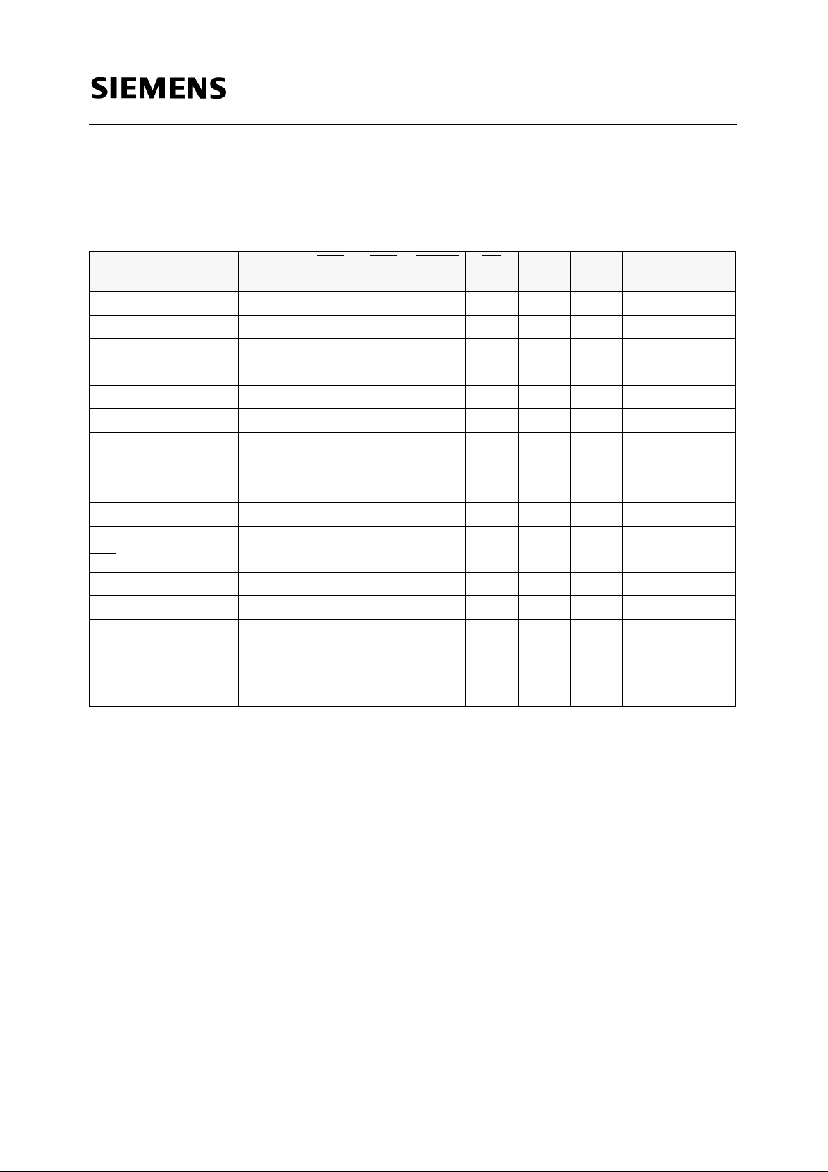
TRUTH TABLE
HYB3164(5)405J/T(L)-50/-60
16M x 4-DRAM
FUNCTION RAS CAS WRITE OE ROW
ADDR
Standby H H - X X X X X High Impedance
Read L L H L ROW COL Data Out
Early-Write L L L X ROW COL Data In
Delayed-Write L L H - L H ROW COL Data In
Read-Modify-Write L L H - L L - H ROW COL Data Out, Data In
Hyper Page Mode Read 1st Cycle L H - L H L ROW COL Data Out
2nd Cycle L H - L H L n/a COL Data Out
Hyper Page Mode Write 1st Cycle L H - L L X ROW COL Data In
2nd Cycle L H - L L X n/a COL Data In
Hyper Page Mode RMW 1st Cycle L H - L H - L L - H ROW COL Data Out, Data In
2st Cycle L H - L H - L L - H n/a COL Data Out, Data In
RAS only refresh L H X X ROW n/a High Impedance
CAS-before-RAS refresh H - L L H X X n/a High Impedance
Test Mode Entry H - L L L X X n/a High Impedance
Hidden Refresh READ L-H-L L H L ROW COL Data Out
WRITE L-H-L L L X ROW COL Data In
Self Refresh
(L-version only)
H - L L H X X X High Impedance
COL
ADDR
I/O1-
I/O4
Semiconductor Group 92
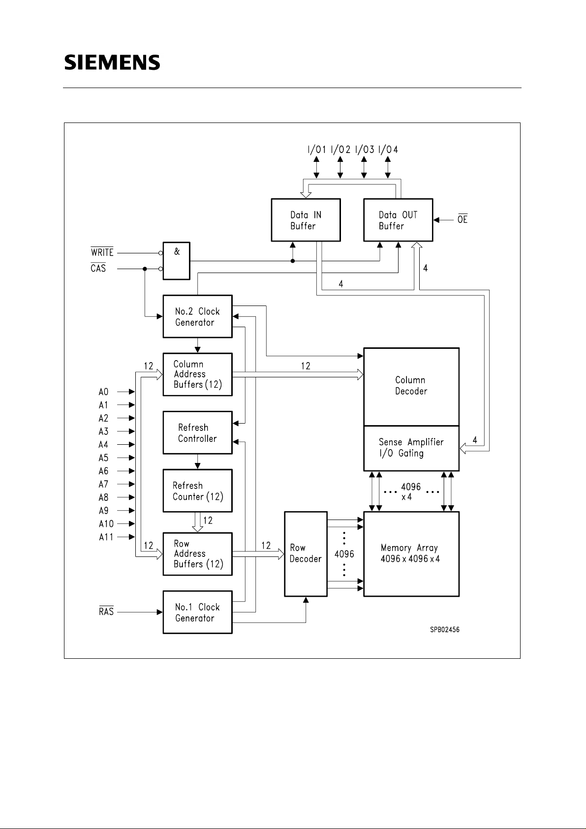
HYB3164(5)405J/T(L)-50/-60
16M x 4-DRAM
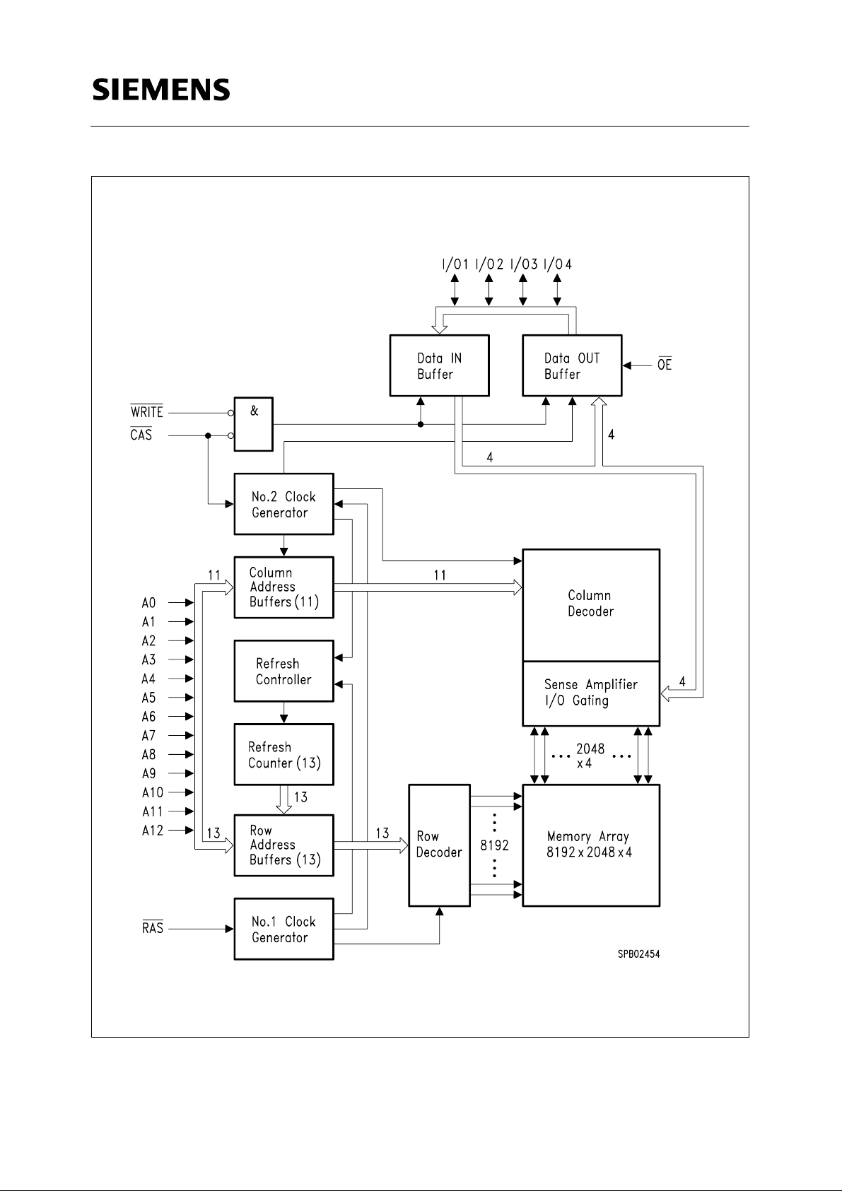
Block Diagram for HYB 3164405J/T(L)
Semiconductor Group 93
HYB3164(5)405J/T(L)-50/-60
16M x 4-DRAM
Block Diagram for HYB 3165405J/T(L)
Semiconductor Group 94
HYB3164(5)405J/T(L)-50/-60
16M x 4-DRAM
Absolute Maximum Ratings
Operating temperature range..............................................................................................0 to 70 ˚C
Storage temperature range.........................................................................................– 55 to 150 ˚C
Input/output voltage..................................................................................-0.5 to min (Vcc+0.5,4.6) V
Power supply voltage....................................................................................................-0.5V to 4.6 V
Power dissipation......................................................................................................................1.0 W
Data out current (short circuit)..................................................................................................50 mA
Note
Stresses above those listed under „Absolute Maximum Ratings“ may cause permanent damage of
the device. Exposure to absolute maximum rating conditions for extended periods may effect device
reliability.
DC Characteristics
T
= 0 to 70 ˚C, VSS = 0 V, VCC = 3.3 V ± 0.3 V, (values in brackets for HYB 3165405J/T)
A
Parameter Symbol Limit Values Unit Note
min. max.
Input high voltage
Input low voltage
Output high voltage (LVTTL)
V
IH
V
IL
V
OH
2.0 Vcc+0.3 V 1)
– 0.3 0.8 V 1)
2.4 – V
Output „H“ level voltage (Iout = -2mA)
Output low voltage (LVTTL)
V
OL
– 0.4 V
Output „L“level voltage (Iout = +2mA)
Output high voltage (LVCMOS)
V
OH
Vcc-0.2 - V
Output „H“ level voltage (Iout = -100uA)
Ouput low voltage (LVCMOS)
V
OL
- 0.2 V
Output „L“ level voltage (Iout = +100uA)
Input leakage current,any input
(0 V < Vin < Vcc , all other pins = 0 V
Output leakage current
(DO is disabled, 0 V < Vout < Vcc )
I
I
I(L)
O(L)
– 2 2 µA
– 2 2 µA
Average Vcc supply current:
-50 ns version
-60 ns version
(RAS, CAS, address cycling: tRC = tRC min.)
Standby Vcc supply current
(RAS=CAS= Vih)
Semiconductor Group 95
I
I
CC1
CC2
–
–
110 (140)
100 (120)mAmA
– 2 mA –
2) 3) 4)
HYB3164(5)405J/T(L)-50/-60
16M x 4-DRAM
DC Characteristics
T
= 0 to 70 ˚C, VSS = 0 V, VCC = 3.3 V ± 0.3 V, (values in brackets for HYB 3165405J/T)
A
(cont’d)
Parameter Symbol Limit Values Unit Note
min. max.
Average Vcc supply current, during RAS-only
refresh cycles: -50 ns version
-60 ns version
(RAS cycling: CAS = VIH: tRC = tRC min.)
Average Vcc supply current, during
hyperpage mode (EDO): -50 ns version
-60 ns version
(RAS = VIL, CAS, address cycling: tHPC=tHPC min.)
Standby Vcc supply current
(RAS=CAS= Vcc-0.2V)
Average Vcc supply current, during
CAS-before-
RAS refresh mode: -50 ns version
-60 ns version
(RAS, CAS cycling: tRC = tRC min.)
Self Refresh Current (L-version only)
Average Power Supply Current during Self Refresh.
(CBR cycle with tRAS>TRASSmin,
WE = Vcc-0.2V, Address and Din=Vcc-0.2V or 0.2V)
CAS held low,
I
I
I
I
I
CC3
CC4
CC5
CC6
CC7
–
–
–
–
110 (140)
100 (120)mAmA
115 (150)
100 (120)mAmA
– 200 A –
–
–
110 (140)
100 (120)mAmA
– 400 A
2) 4)
2) 3) 4)
2) 4)
Capacitance
T
= 0 to 70 ˚C,VCC = 3.3 V ± 0.3 V, f = 1 MHz
A
Parameter Symbol Limit Values Unit
min. max.
Input capacitance (A0 to A11,A12)
Input capacitance (
RAS, CAS, WRITE, OE) C
I/O capacitance (I/O1-I/O4)
C
I1
I2
C
IO
–5pF
–7pF
–7pF
Semiconductor Group 96
HYB3164(5)405J/T(L)-50/-60
16M x 4-DRAM
AC Characteristics
T
= 0 to 70 ˚C,VCC = 3.3 V ± 0.3V , tT = 2 ns
A
5)6)
Parameter
common parameters
Random read or write cycle time t
RAS precharge time t
RAS pulse width t
CAS pulse width t
Row address setup time t
Row address hold time t
Column address setup time t
Column address hold time t
RAS to CAS delay time t
RAS to column address delay time t
RAS hold time t
CAS hold time t
CAS to RAS precharge time t
Transition time (rise and fall) t
Refresh period for HYB3164405 t
Refresh period for HYB3165405 t
Symbol
RC
RP
RAS
CAS
ASR
RAH
ASC
CAH
RCD
RAD
RSH
CSH
CRP
T
REF
REF
Limit Values
Unit Note
-50 -60
min. max. min. max.
84 – 104 – ns
30 – 40 – ns
50 100k 60 100k ns
8 10k 10 10k ns
0–0– ns
8–10– ns
0–0– ns
8–10– ns
12 37 14 45 ns
10 25 12 30 ns
810–ns
45 50 – ns
5–5– ns
1 50 1 50 ns 7
– 128 – 128 ms
– 64 – 64 ms
Read Cycle
Access time from RAS t
Access time from
CAS t
Access time from column address t
OE access time t
Column address to
RAS lead time t
Read command setup time t
Read command hold time t
Read command hold time referenced to
RAC
CAC
AA
OEA
RAL
RCS
RCH
t
RRH
RAS
Semiconductor Group 97
– 50 – 60 ns 8, 9
– 13 – 15 ns 8, 9
– 25 – 30 ns 8,10
– 13 – 15 ns
25 – 30 – ns
0–0– ns
0–0– ns11
0–0– ns11
HYB3164(5)405J/T(L)-50/-60
16M x 4-DRAM
AC Characteristics
T
= 0 to 70 ˚C,VCC = 3.3 V ± 0.3V , tT = 2 ns
A
(cont’d)
5)6)
Parameter
CAS to output in low-Z t
Output buffer turn-off delay t
Output buffer turn-off delay from
Data to
Data to
CAS low delay t
OE low delay t
OE t
CAS high to data delay t
OE high to data delay t
Write Cycle
Write command hold time t
Write command pulse width t
Write command setup time t
Write command to
Write command to
RAS lead time t
CAS lead time t
Data setup time t
Data hold time t
Symbol
CLZ
OFF
OEZ
DZC
DZO
CDD
ODD
WCH
WP
WCS
RWL
CWL
DS
DH
Limit Values
Unit Note
-50 -60
min. max. min. max.
0–0– ns8
0 13 0 15 ns 12
0 13 0 15 ns 12
0–0– ns13
0–0– ns13
13 – 15 – ns 14
13 – 15 – ns 14
8–10– ns
7–10– ns
0–0– ns15
8–10– ns
8–10– ns
0–0– ns16
7 – 10 – ns 16
Read-modify-Write Cycle
Read-write cycle time t
RAS to WE delay time t
CAS to WE delay time t
Column address to
WE delay time t
OE command hold time t
RWC
RWD
CWD
AWD
OEH
Hyper Page Mode (EDO) Cycle
Hyper page mode (EDO) cycle time t
CAS precharge time t
Access time from
CAS precharge t
Output data hold time t
RAS pulse width in hyper page mode t
HPC
CP
CPA
COH
RAS
Semiconductor Group 98
111 – 135 – ns
67 – 79 – ns 15
30 – 34 – ns 15
42 – 49 – ns 15
7–10– ns
20 – 25 – ns
8–10– ns
– 27 – 35 ns 7
5–5– ns
50 200k 60 200k ns
 Loading...