

Siemens CLY5 Datasheet
GaAs FET CLY 5
________________________________________________________________________________________________________
D a t a s h e e t
*Power amplifier for mobile phones
*For frequencies from 400 MHz to 2.5 GHz
*Wide operating voltage range: 2.7 to 6 V
* P
at V
=3V, f=1.8GHz typ. 26.5 dBm
*High efficiency better 55 %
ESD: Electrostatic discharge sensitive device,
observe handling precautions!
Type Marking Ordering code
(taped)
CLY 5 CLY 5 Q62702-L90 G S D S SOT 223
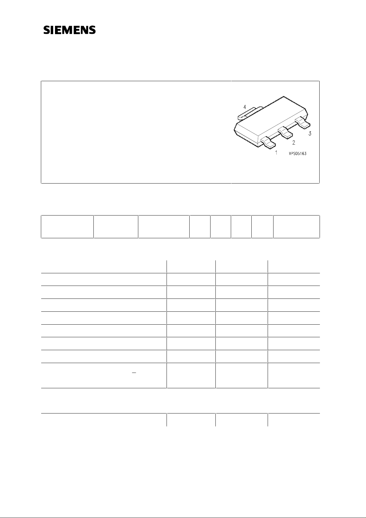
Pin Configuration
1 2 3 4
Package 1)
Maximum ratings Symbol Values Unit
Drain-source voltage V
Drain-gate voltage V
Gate-source voltage V
Drain current I
Channel temperature T
Storage temperature T
Pulse peak power P
Total power dissipation (T
Ts: Temperature at soldering point
< 80 °C)
s
Pulse
P
DS
DG
GS
D
Ch
stg
tot
9V
12 V
-6 V
1.2 A
150 °C
-55...+150 °C
9W
2W
Thermal Resistance
Channel-soldering point R
1) Dimensions see chapter Package Outlines
Siemens Aktiengesellschaft pg. 1/8 17.12.96
thChS
≤35
K/W
HL EH PD21
GaAs FET CLY 5
________________________________________________________________________________________________________
Electrical characteristics (TA = 25°C , unless otherwise specified)
Characteristics Symbol min typ max Unit
Drain-source saturation current
V
DS
= 3 V
= 0 V
V
GS
Drain-source pinch-off current
V
DS
= 3 V
V
GS
= -3.8 V
Gate pinch-off current
V
DS
= 3 V
V
GS
= -3.8 V
Pinch-off Voltage
V
DS
= 3 V
=100µA
I
D
Small Signal Gain*)
= 3 V
V
DS
Pin = 0 dBm
= 350 mA f = 1.8 GHz
I
D
Small Signal Gain*)
= 5 V
V
DS
Pin = 0 dBm
= 350 mA f = 1.8 GHz
I
D
Small Signal Gain **)
= 3 V
V
DS
Pin = 0 dBm
= 350 mA f = 1.8 GHz
I
D
I
DSS
I
I
V
GS(p)
G
G
G
D
G
600 800 1200 mA
- 10 100 µA
-520µA
-3.8 -2.8 -1.8 V
10.5 11.0 - dB
11.5 12.0 - dB
p
9.0 9.5 - dB
Output Power
= 3 V
V
DS
Pin = 19 dBm
= 350 mA f = 1.8 GHz
I
D
Output Power
= 5 V
V
DS
Pin = 21 dBm
= 350 mA f = 1.8 GHz
I
D
1dB-Compression Point
V
DS
= 3 V
= 350 mA f = 1.8 GHz
I
D
1dB-Compression Point
V
DS
= 5 V
= 350 mA f = 1.8GHz
I
D
Power Added Efficiency
= 5 V
V
DS
Pin = 21 dBm
*) Matching conditions for maximum small signal gain (not identical with power matching conditions!)
**) Power matching conditions: f=1.8GHz:
Source Match: Γ
= 350 mA f = 1.8 GHz
I
D
: MAG 0.58; ANG -143°; Load Match: Γml : MAG 0.76; ANG -116°
ms
P
P
P
o
P
o
1dB
1dB
26.5 27 - dBm
29.5 30 - dBm
- 26.5 - dBm
- 30 - dBm
PAE 40 55 - %
Siemens Aktiengesellschaft pg. 2/8 17.12.96
HL EH PD21
GaAs FET CLY 5
V
V
________________________________________________________________________________________________________
Compression Power vs. Drain-Source Voltage
f = 1.8GHz; IDS=0.5IDSS
P1dB
40
[dBm]
35
30
25
20
15
10
5
0
012345678
Drain-Source Voltage
[V]
ηη
D
80
[%]
70
60
50
40
30
20
10
0
Gain
16
[dB]
14
12
10
8
6
4
2
0
012345678
Drain-Source Voltage
P1dB
2.0
[W]
1.75
1.5
1.25
1.0
0.75
0.5
0.25
0
[V]
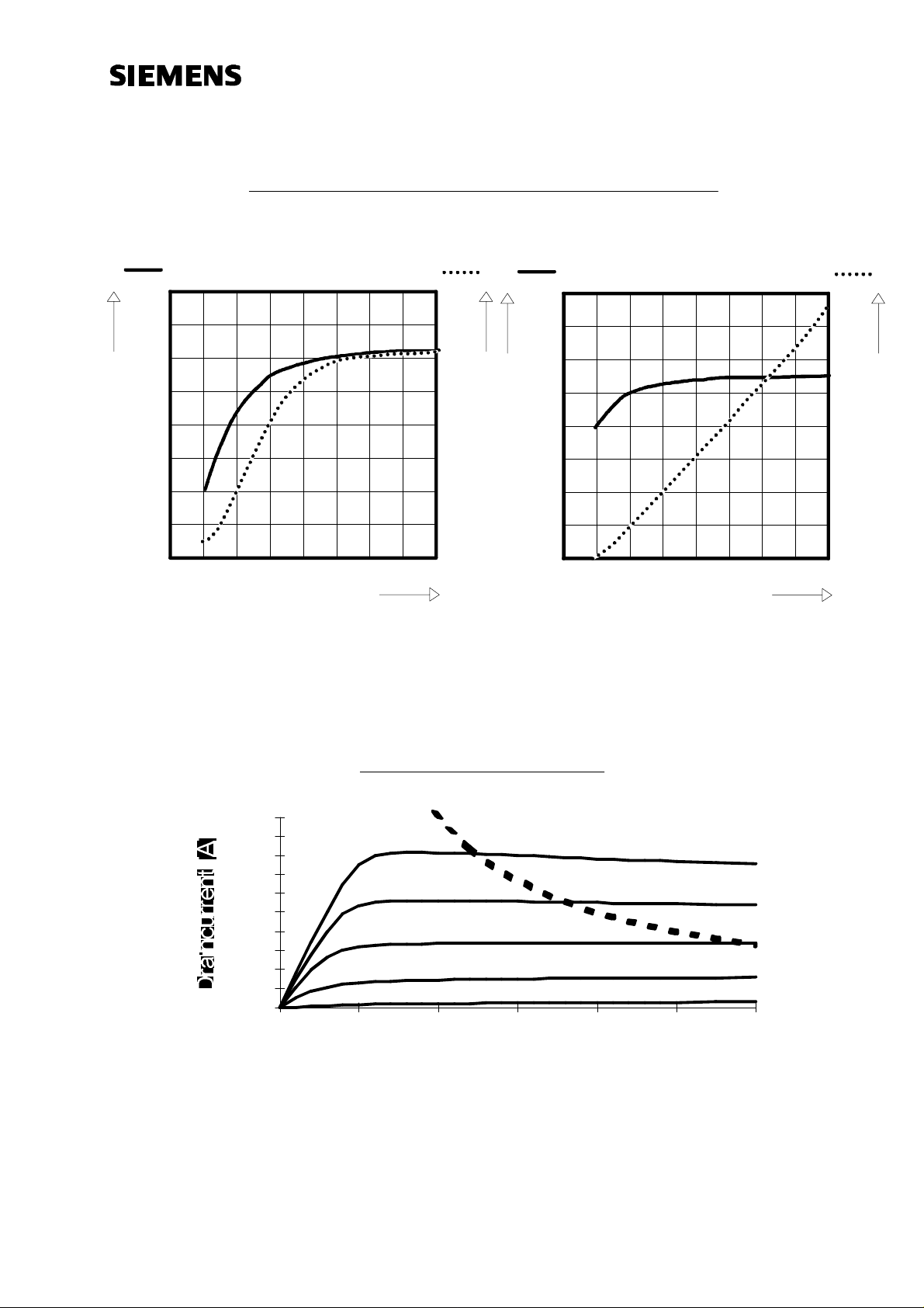
Output Characteristics
PtotDC
0,9
0,7
0,5
0,3
0,1
0
0123456
Drain-Source Voltage [V]
Siemens Aktiengesellschaft pg. 3/8 17.12.96
VGS = 0V
VGS = -0.5
VGS = -1V
VGS = -1.5
VGS = -2V
HL EH PD21
 Loading...