

Siemens CLY15 Datasheet
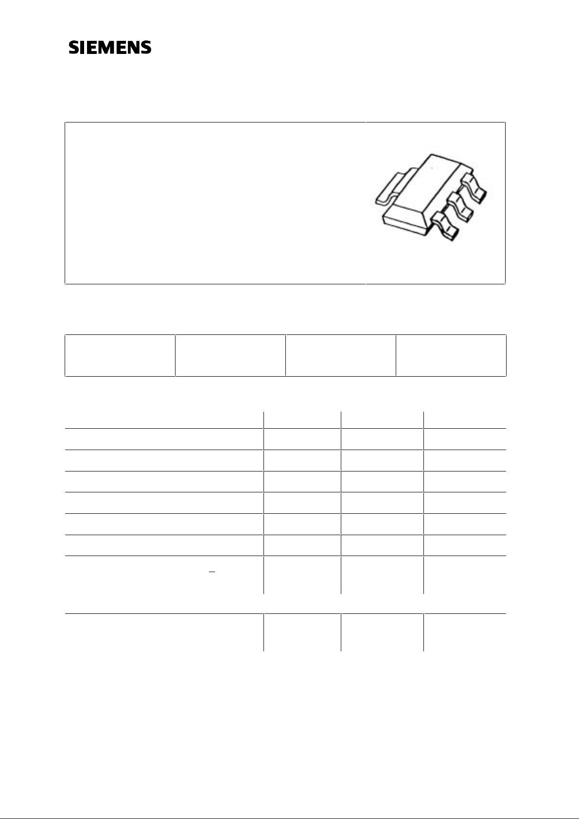
GaAs FET CLY 15
________________________________________________________________________________________________________
D a t a s h e e t
*Power amplifier for mobile phones
*For frequencies from 400 MHz to 2.5 GHz
*Operating voltage range: 2.7 to 6 V
* P
at V
=3V, f=1.8 GHz typ. 31.5 dBm
*Efficiency better 50%
ESD: Electrostatic discharge sensitive device,
observe handling precautions!
S
D
S
G
Type Marking Ordering code
(taped)
Package 1)
CLY 15 CLY 15 Q62702-L99 SOT 223
Maximum ratings Symbol Unit
Drain-source voltage V
Drain-gate voltage V
Gate-source voltage V
Drain current I
Channel temperature T
Storage temperature T
Total power dissipation (Ts < 80°C)
Ts: Temperature at soldering point
P
DS
DG
GS
D
Ch
stg
tot
9V
12 V
-6 V
5A
150 °C
-55...+150 °C
4.7 W
Thermal resistance
R
thChS
< 15 K/W
Channel-soldering point (GND)
1) Dimensions see chapter Package Outlines
Siemens Aktiengesellschaft pg. 1/7 09/96
HL EH PD 21
GaAs FET CLY 15
________________________________________________________________________________________________________
Electrical characteristics (TA = 25°C , unless otherwise specified)
Characteristics Symbol min typ max Unit
Drain-source saturation current *)
= 3V
V
DS
= 0V
V
GS
Cut-off current
= 3V
V
DS
V
GS
= -3.8V
Gate cut-off current
= 3V
V
DS
V
GS
= -3.8V
Pinch-off Voltage
VDS=3V ID=400µA
Small Signal Gain *)
= 3V
V
DS
Pin = 5dBm
= 1.4A f = 1.8GHz
I
D
Output Power *)
= 3V
V
DS
Pin = 29dBm
= 1.4A f = 1.8GHz
I
D
Output Power *)
= 5V
V
DS
Pin = 30 dBm
= 1.4A f = 1.8GHz
I
D
I
DSS
I
I
V
GS(p)
G
P
P
D
G
2.4 3.2 4.8 A
- - 400 µA
-2070µA
-3.8 -2.8 -1.8 V
dB
-6-
o
o
32 32.5 - dBm
34.5 35 - dBm
1dB-Compression Point *)
= 3V
V
DS
= 1.4A f = 1.8GHz
I
D
1dB-Compression Point *)
= 5V
V
DS
= 1.4A f = 1.8GHz
I
D
Power Added Efficiency *)
VDS = 3V ID = 1.4A f = 1.8GHz
Pin = 29dBm
*) pulsed measurement; duty cycle 1:10; ton = 1ms, power matching conditions.
Siemens Aktiengesellschaft pg. 2/7 09/96
P
P
1dB
1dB
η
D
- 31.5 - dBm
- 34.5 - dBm
45 50 - %
HL EH PD 21
GaAs FET CLY 15
________________________________________________________________________________________________________
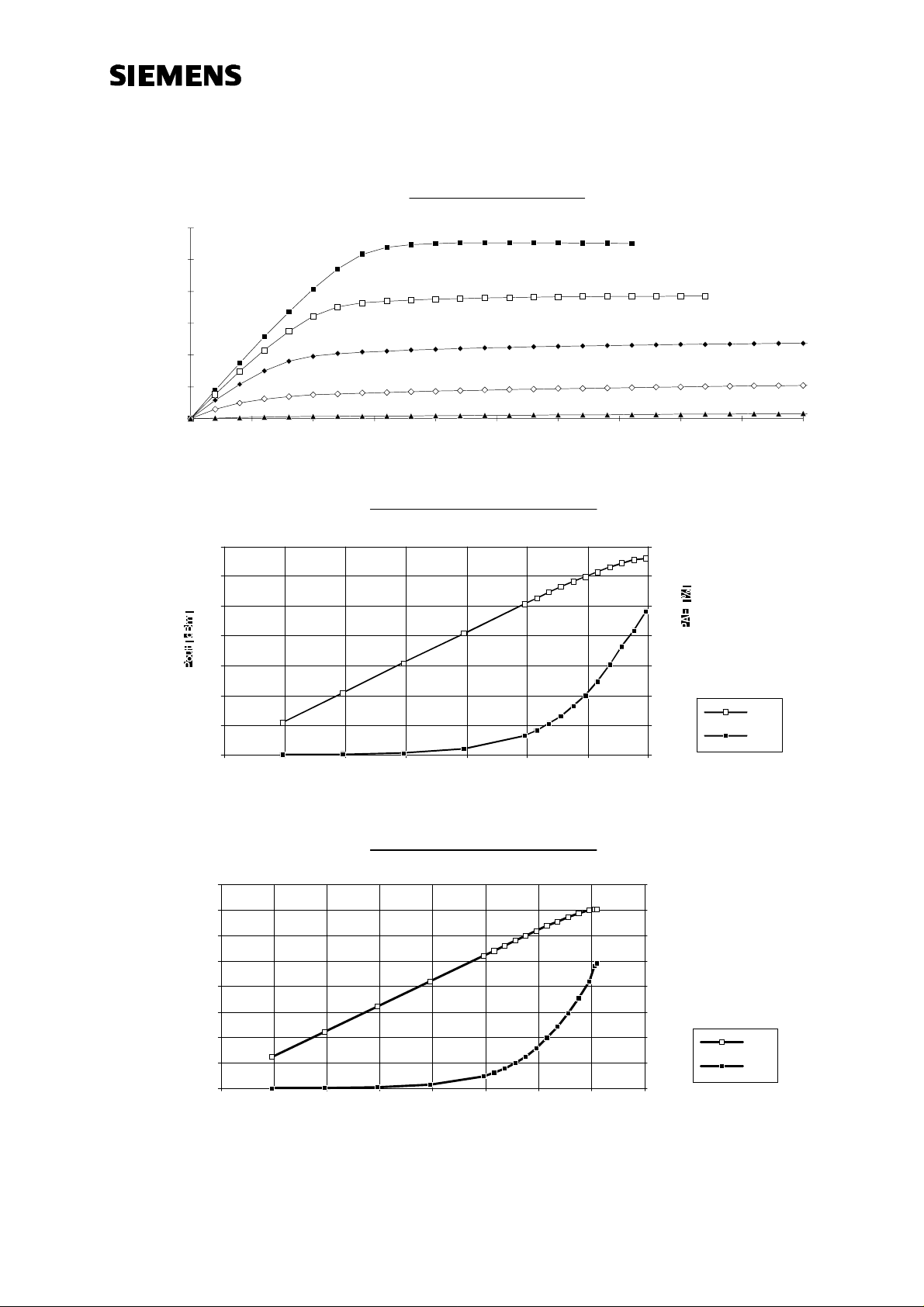
Output Charateristics
3
VGS = 0V
2,5
VGS = -0.5V
2
1,5
ID [A]
1
0,5
0
0 0,5 1 1,5 2 2,5 3 3,5 4 4,5 5
VDS [V]
Power Characteristics
35
30
25
20
15
70
60
50
40
30
@ 3V/1.4A
VGS = -1V
VGS = -1.5V
VGS = -2V
10
5
0
-5 0 5 10 15 20 25 30
Pin [dBm]
Power Characteristics
40
35
30
25
20
15
Pout [dBm]
10
5
0
-5 0 5 10 15 20 25 30 35
Pin [dBm]
20
10
0
80
70
60
50
40
30
20
10
0
Pout
PAE
@ 5V/1.4A
PAE [%]
Pout
PAE
Siemens Aktiengesellschaft pg. 3/7 09/96
HL EH PD 21
 Loading...