

Siemens BTS 780 Technical data
现货库存、技术资料、百科信息、热点资讯,精彩尽在鼎好!
TrilithIC
Target Data
Overview
Features
• Quad switch driver
• Free configurable as bridge or quad-switch
• Optimized for DC motor management applications
• Ultra low
R
High-side switch: typ. 35 mΩ,
Low-side switch: typ. 15 mΩ
• Very high peak current capability
• Very low quiescent cu rrent
• Space- and thermal optimized SMD-Power-Package
• Load and GND-short-circuit-protec ted
• Operates up to 40 V
• 2-Bit status flag diagnosis
• Overtemperature shut down with hysteresis
• Short-circuit detection and diagnosis
• Open-load detection and diagnosis
• C-MOS compatible inputs
• Internal clamp diodes
• Isolated sources fo r external current sensing
• Over- and under-voltage detection wi th hyste r esi s
DS ON
@25°C:
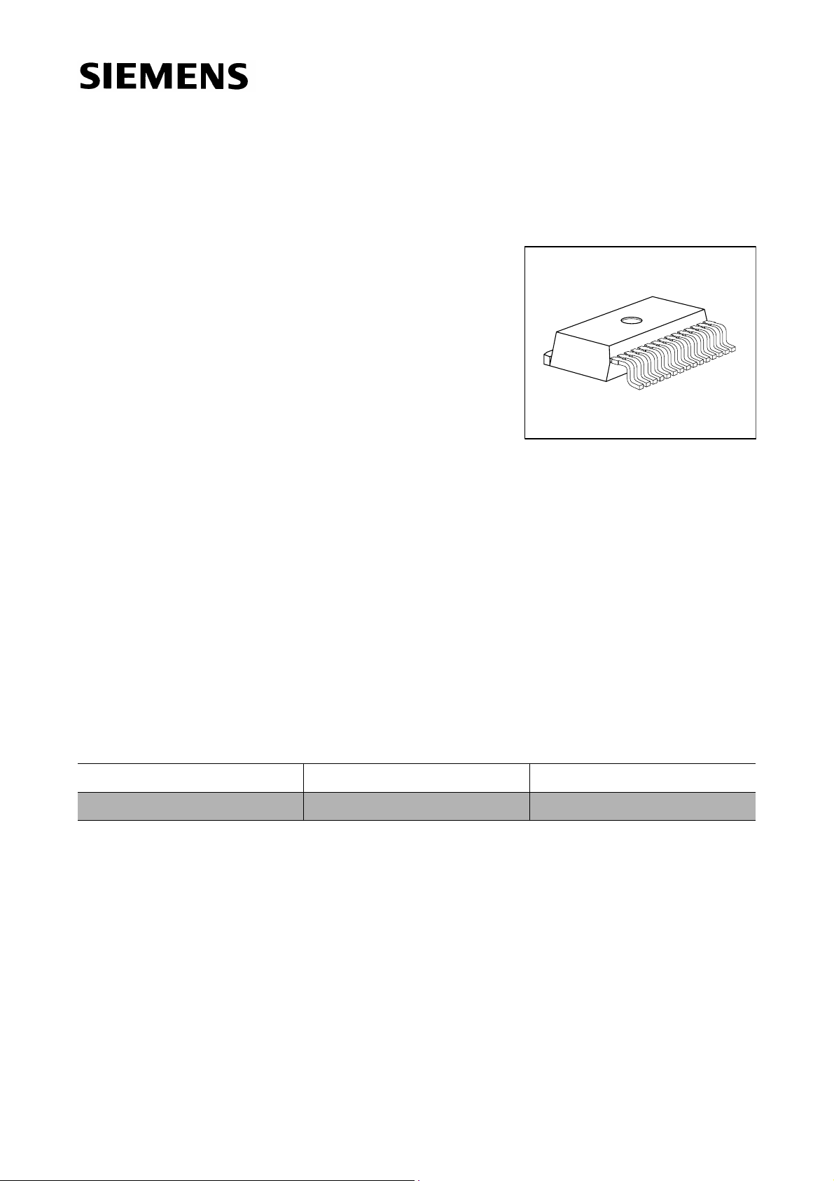
BTS 780
P-TO263-15-1
Type Ordering Code Package
BTS 780 on request P-TO263-15-1
Description
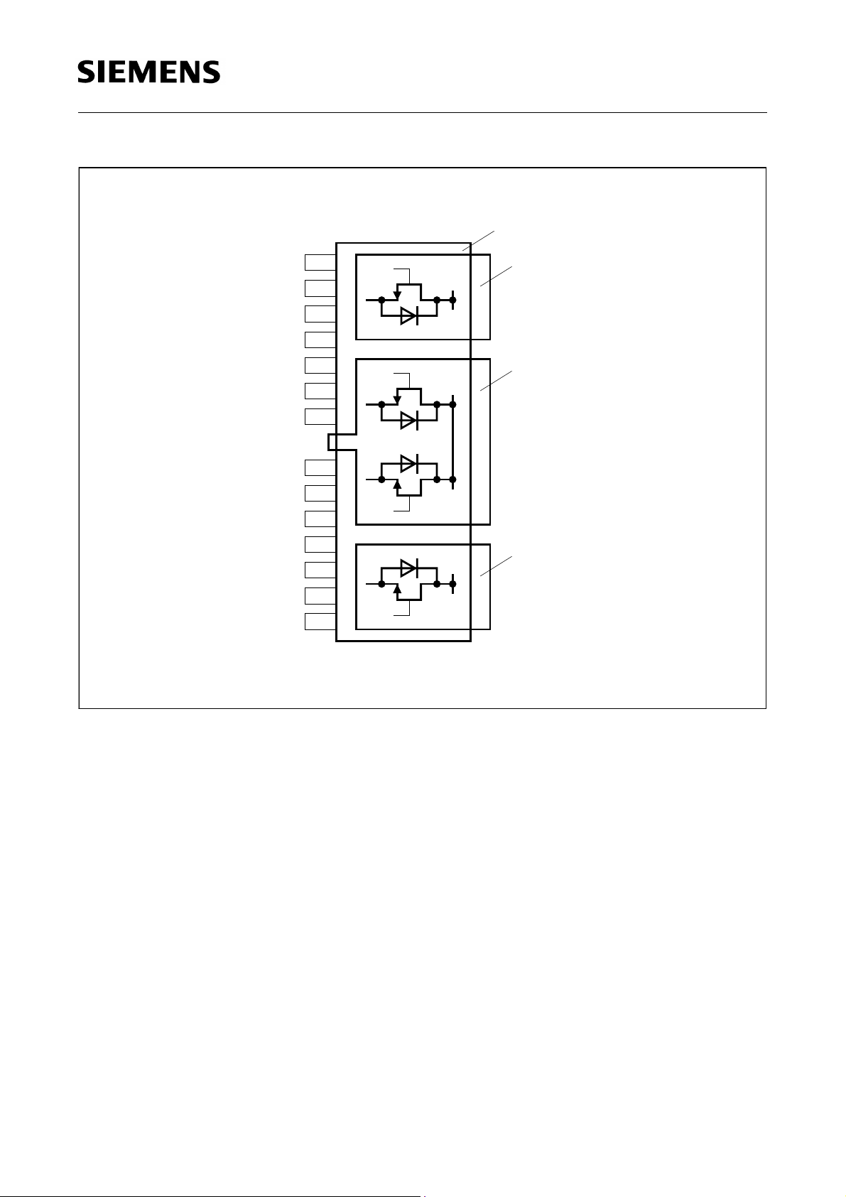
The BTS 780 is a TrilithIC contains one double high-side switch and two low-side
switches in one P-TO263-15-1.
“Silicon instead of heatsink”
becomes true
The ultra low
R
of this device avoids powerdissipation. It saves costs in mechanical
DS ON
construction and mounting and increases the efficiency.
®
The high-side switches are produced in the SIEMENS SMART SIPMOS
technology. It
is fully protected and contains the signal conditioning circuitry for diagnosis (the
comparable standard high-side product is the BTS 734L1).
Semiconductor Group 1 1998-02-01

BTS 780
For minimized R
the two low-side switches are produced in the SIEMENS S-Fet
DS ON
logic level technology (the comparable standard product is the BUZ 100SL).
Each drain of these three chips is mounted on separated leadframes (see pin
configuration). The sources of all four power transistors are connected to separate pins.
So the BTS 780 can be used in H-Bridge configuration as well as in any other switch
configuration.
Moreover, it is possible to add current sense resistors.
All these features open a broad range of automotive and industrial applications.
Semiconductor Group 2 1998-02-01
BTS 780
Molding
Compound
SL1 1
SL1 2
17
GL1 3
GND 4
Heat-Slug 1
DL1
GH1
ST1
SH1
GND
GH2
ST2
SH2
SL2
SL2
GL2
5
6
7
8
9
10
11
12
13
14
Figure 1 Pin Configuration (top view)
AEP02224
16
15
Heat-Slug 2
DHVS
Heat-Slug 3
DL2
Semiconductor Group 3 1998-02-01
Pin Definitions and Functions
Pin No. Symbol Function
1, 2 SL1 Source of low-side switch 1
3 GL1 Gate of low-side switch 1
4, 8 GND Ground
5 GH1 Gate of high-side switch 1
6 ST1 Status of high-side switch 1; open Drain output
7 SH1 Source of high-side switch 1
9 GH2 Gate of high-side switch 2
10 ST2 Status of high-side switch 2; open Drain output
11 SH2 Source of high-side switch 2
BTS 780
12, 13 SL2 Source of low-side switch 2
14 GL2 G ate of low-side switch 2
15 DL2 Drain of low-side switch 2
Heat-Slug 3 or Heat-Dissipator
16 DHVS Drain of high-side switches and power supply voltage
Heat-Slug 2 or Heat-Dissipator
17 DL1 Drain of low-side switch 1
Heat-Slug 1 or Heat-Dissipator
Bold type: Pin needs power wiring
Semiconductor Group 4 1998-02-01
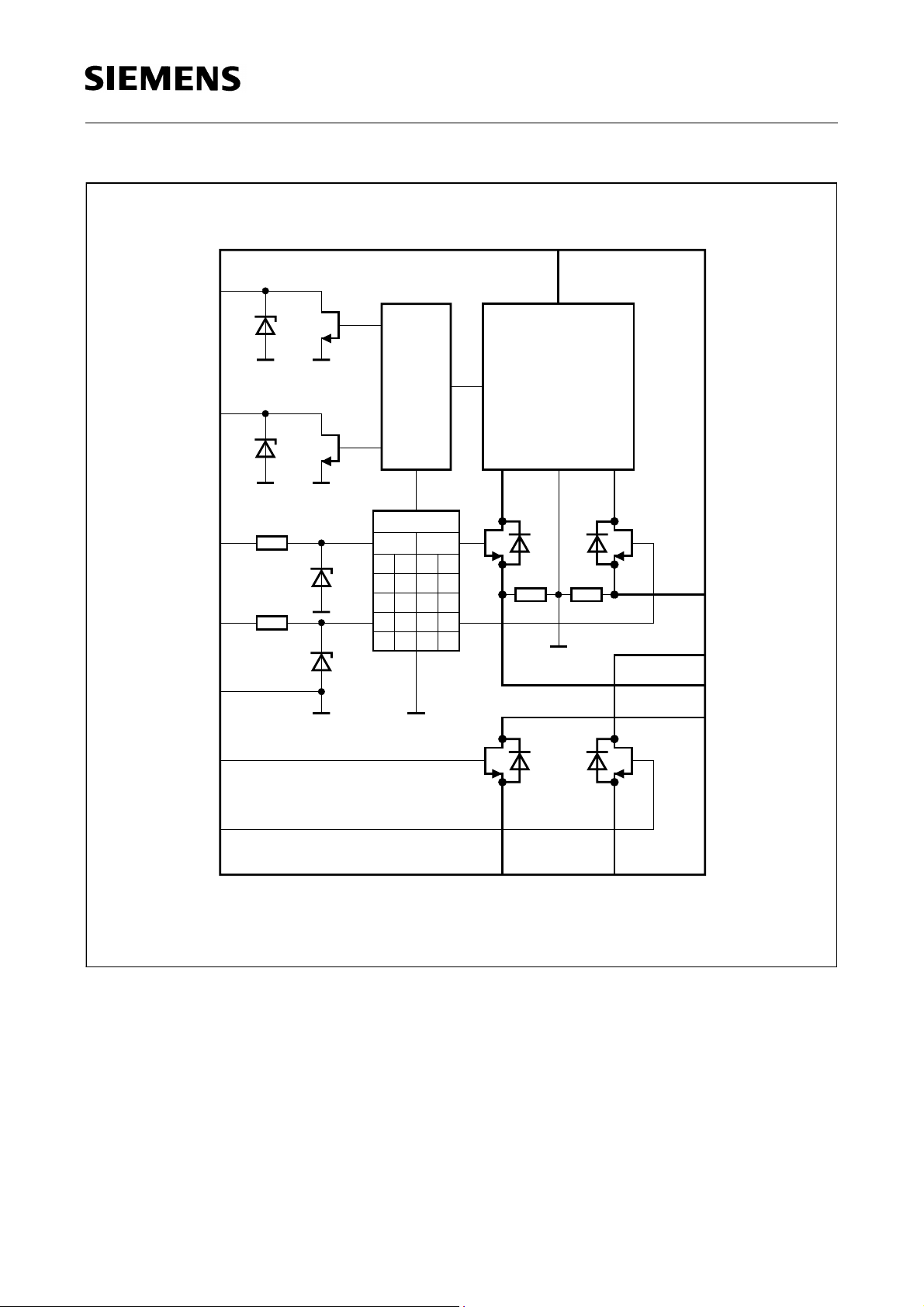
ST1
BTS 780
DVHS
Heat-Slug 2
16
6
DST1
C6V1
ST2
GH1
GH2
GND
GL1
GL2
10
5
9
4, 8
3
14
DST2
C6V1
R
I1
3.5 kΩ
R
I2
Diagnosis
Biasing and Protection
Driver
IN OUT
1212
DI1
00
C6V1
0
1
Ωk3.5
LL
1
HL
0
LH
11
HH
DI2
C6V1
R
O1
R
10 kΩ Ωk10
O2
Heat-Slug 3
Heat-Slug 1
11
15
17
7
SH2
DL2
SH1
DL1
1, 2 12, 13
SL1 SL2
AEB02225
Figure 2 Block Diagram
Semiconductor Group 5 1998-02-01

BTS 780
Circuit Description
Input Circuit
The control inputs GH1,2 consist of TTL/CMOS compatible Schmitt-Triggers with
hysteresis. Buffer amplifiers are driven by these stages and convert the logic signal into
the necessary form for driving the power output stages.
The inputs GH1 and GH2 are connected to a standard N-channel logic level power-MOS
gate.
Output Stages
The output stages consist of an ultra low
R
Power-MOS H-Bridge. Protective circuits
DS ON
make the outputs short-circ uit proof to gro und and loa d short-ci rcuit pr oof. Positi ve and
negative voltage spikes, which occur when driving inductive loads, are limited by
integrated power clamp diodes.
Short-Circuit Protection (valid only for the high-side switches)
The outputs are protected against
– output short circuit to ground, and
– overload (load short circuit).
An internal OP-Amp controls the Drain-Source-Voltage of the HS-Switches by
comparing the DS-Voltage-Dro p with a n interna l referenc e voltage. Ab ove thi s trippoi nt
the OP-Amp reduces the output current depending on the junction temperature and the
drop voltage.
In the case of an overloaded high-side switch the corresponding status output is set to
low.
R
If the HS-Switches are in OFF-state-Condition internal resistors
from SH1,2 to GND
O1,2
pull the voltage at SH1,2 to low values. On each output pin SH1 and SH2 an output
examiner circuit compa re s the outp ut vol t age s with the internal reference vo ltage VEO.
This results in switching the corres ponding status ou tput to low if the source vo ltage in
OFF-Condition is higher then VEO. In H-Brid ge condition this feature can be used to
protect the low-side switches against short circuit during the OFF-period.
Overtemperature Protection (valid only for the high-side-switches)
The chip also inco rporates an overtem perature protecti on circuit with h ysteresis which
switches off the output transistors and sets the status output to low.
Semiconductor Group 6 1998-02-01
 Loading...