

现货库存、技术资料、百科信息、热点资讯,精彩尽在鼎好!
TrilithIC BTS 775 G
Overview
Features
• Quad switch driver
• Free configurable as bridge or quad-switch
• Optimized for DC motor management applications
• Ultra low
R
High-side switch: typ.85 mΩ,
Low-side switch: typ. 45 mΩ
• Very high peak current capability
DS ON
@25°C:
P-DSO-28-9
• Very low quiescent current
• Space- and thermal optimized power P-DSO-Package
• Full short-circuit-protection
• Operates up to 40 V
• Status flag diagnosis
• Overtemperature shut down with hysteresis
• Short-circuit detection and diagnosis
• Open-load detection and diagnosis
• C-MOS compatible inputs
• Internal clamp diodes
• Isolated sources for external current sensing
• Over- and under-voltage detection with hysteresis
Type Ordering Code Package
BTS 775 G Q67007-A9350 P-DSO-28-9
Description
The BTS 775 G is a TrilithIC contains one double high-side switch and two low-side
switches in one P-DSO-28-9 -Package.
“Silicon instead of heatsink”
becomes true
The ultra low
R
of this device avoids powerdissipation. It saves costs in mechanical
DS ON
construction and mounting and increases the efficiency.
®
The high-side switches are produced in the SIEMENS SMART SIPMOS
technology. It
is fully protected and contains the signal conditioning circuitry for diagnosis. (The
comparable standard high-side product is the BTS 621L1.)
Semiconductor Group 1 1999-01-07

BTS 775 G
For minimized R
SIEMENS SMART SIPMOS
the two low-side switches are N channel vertical power FETs in the
DS ON
®
technology. Fully protected by embedded protection
functions. (The comparable standard product is the BSP 78).
Each drain of these three chips is mounted on separated leadframes (see P-DSO-28-9
pin configuration). The sources of all four power transistors are connected to separate
pins.
So the BTS 775 G can be used in H-Bridge configuration as well as in any other switch
configuration.
Moreover, it is possible to add current sense resistors.
All these features open a broad range of automotive and industrial applications.
Semiconductor Group 2 1999-01-07
BTS 775 G
DL1
GL1
DL1
N.C.
DHVS
GND
GH1
ST
GH2
DHVS
N.C.
DL2
1
2
3
425
5
6
7
8
9
10
11
12
LS-Lead Frame 1
HS-Lead Frame
LS-Lead Frame 2
28
27
26
24
23
22
21
20
19
18
17
DL1
SL1
SL1
DL1
DHVS
SH1
SH1
SH2
SH2
DHVS
DL2
SL2
GL2
DL2
13
14
AEP02071
16
15
SL2
DL2
Figure 1 Pin Configuration (top view)
Semiconductor Group 3 1999-01-07
BTS 775 G
Pin Definitions and Functions
Pin No. Symbol Function
1, 3, 25, 28 DL1 Drain of low-side switch1
Leadframe 1
2 GL1 Gate of low-side switch1
4 N.C. not connected
5, 10, 19, 24 DHVS Drain of high-side switches and power supply voltage
Leadframe 2
6 GND Ground
7 GH1 Gate of high-side switch1
8 ST Status of high-side switches; open Drain output
9 GH2 Gate of high-side switch2
1)
1)
11 N.C. not connected
12, 14, 15, 18 DL2 Drain of low-side switch2
Leadframe 3
1)
13 GL2 Gate of low-side switch2
16, 17 SL2 Source of low-side switch2
20, 21 SH2 Source of high-side switch2
22, 23 SH1 Source of high-side switch1
26, 27 SL1 Source of low-side switch1
1)
To reduce the thermal resistance these pins are direct connected via metal bridges to the leadframe.
Bold type: Pin needs power wiring
Semiconductor Group 4 1999-01-07
ST
BTS 775 G
DHVS
2419,10,5,
8
GH1
GH2
GND
GL1
Diagnosis
7
9
6
2
Driver
IN OUT
00
0
1
0
1
11
Protection
Gate
Driver
LL
HL
LH
HH
Biasing and Protection
R
O1 O2
Protection
R
2120,
1815,14,12,
22, 23
25, 283,1,
SH2
DL2
SH1
DL1
GL2
13
SL1 SL2
Gate
Driver
26, 16,27 17
AEB02676
Figure 2 Block Diagram
Semiconductor Group 5 1999-01-07

BTS 775 G
Circuit Description
Input Circuit
The control inputs GH1,2 consist of TTL/CMOS compatible Schmitt-Triggers with
hysteresis. Buffer amplifiers are driven by these stages and convert the logic signal into
the necessary form for driving the power output stages.
The inputs GL1 and GL2 are connected to the internal gate-driving units of the fully
protected N-channel vertical power-MOS-FETs.
Output Stages
The output stages consist of an ultra low
R
Power-MOS H-Bridge. Embedded
DS ON
protective circuits make the outputs short circuit proof to ground, to the supply voltage
and load short circuit proof. Positive and negative voltage spikes, which occur when
driving inductive loads, are limited by integrated power clamp diodes.
Short Circuit Protection
The outputs are protected against
– output short circuit to ground
– output short circuit to the supply voltage, and
– overload (load short circuit).
An internal OP-Amp controls the Drain-Source-Voltage by comparing the DS-VoltageDrop with an internal reference voltage. Above this trippoint the OP-Amp reduces the
output current depending on the junction temperature and the drop voltage.
In the case of overloaded high-side switches the status output is set to low.
R
If the HS-Switches are in OFF-state-Condition internal resistors
from SH1,2 to GND
O1,2
pull the voltage at SH1,2 to low values. On each output pin SH1 and SH2 an output
examiner circuit compares the output voltages with the internal reference voltage VEO.
This results in switching the status output to low. The fully protected low-side switches
have no status output.
Overtemperature Protection
The highside and the lowside switch also incorporates an overtemperature protection
circuit with hysteresis which switches off the output transistors and sets the status output
to low.
Undervoltage-Lockout (UVLO)
V
When
reaches the switch-on voltage V
S
The High-Side output transistors are switched off if the supply voltage
the switch off value
Semiconductor Group 6 1999-01-07
V
UVOFF
.
the IC becomes active with a hysteresis.
UVON
V
drops below
S

BTS 775 G
Overvoltage-Lockout (OVLO)
V
When
reaches the switch-off voltage V
S
switched off with a hysteresis. The IC becomes active if the supply voltage
below the switch-on value
V
OVON
.
Open Load Detection
Open load is detected by current measurement. If the output current drops below an
internal fixed level the error flag is set with a delay.
Status Flag
Various errors as listed in the table “Diagnosis” are detected by switching the open drain
output ST to low.
the High-Side output transistors are
OVOFF
V
drops
S
Semiconductor Group 7 1999-01-07

BTS 775 G
Truthtable and Diagnosis (valid only for the High-Side-Switches)
Flag GH1 GH2 SH1 SH2 ST Remarks
Inputs Outputs
Normal operation;
identical with functional truth table
Open load at high-side switch1
Open load at high-side switch2
Short circuit to DHVS at high-side switch1
Short circuit to DHVS at high-side switch2
Overtemperature high-side switch1 0
Overtemperature high-side switch2 X
0
0
1
1
0
0
1
0
1
X
0
0
1
0
1
X
1
X
0
1
0
1
0
1
X
0
0
1
0
1
X
0
0
1
X
X
0
1
L
L
H
H
Z
Z
H
L
H
X
H
H
H
L
H
X
L
L
X
X
L
H
L
H
L
H
X
Z
Z
H
L
H
X
H
H
H
X
X
L
L
1
stand-by mode
1
switch2 active
1
switch1 active
1
both switches
active
1
1
0
detected
1
1
0
detected
0
detected
1
1
0
detected
1
1
1
0 detected
1
0 detected
Overtemperature both high-side switch 0
X
1
Over- and Under-Voltage X X L L 1 not detected
Inputs: Outputs: Status:
0 = Logic LOW Z = Output in tristate condition 1 = No error
1 = Logic HIGH L = Output in sink condition 0 = Error
X = don’t care H = Output in source condition
X = Voltage level undefined
0
1
X
L
L
L
L
L
L
1
0
0
detected
detected
Semiconductor Group 8 1999-01-07

Electrical Characteristics
Absolute Maximum Ratings
– 40 °C <
T
< 150 °C
j
Parameter Symbol Limit Values Unit Remarks
min. max.
High-Side-Switches (Pins DHVS, GH1,2 and SH1,2)
BTS 775 G
Supply voltage
HS-drain current
HS-input current
HS-input voltage
V
I
I
V
S
DHS
GH
GH
– 0.3 43 V –
– 10 * A * internally limited
– 2 2 mA Pin GH1 and GH2
– 10 16 V Pin GH1 and GH2
Status Output ST
Status Output current
I
ST
– 5 5 mA Pin ST
Low-Side-Switches (Pins DL1,2, GL1,2 and SL1,2)
Break-down voltage
LS-drain current
LS-input voltage
V
(BR)DSS
I
DLS
V
GL
40 – V VGS= 0 V; ID<= 1 mA
16 * A * internally limited
– 0.3 10 V Pin GL1 and GL2
Temperatures
Junction temperature
T
j
– 40 150 °C–
Storage temperature
T
stg
– 50 150 °C–
Thermal Resistances (one HS-LS-Path active)
LS-junction case
HS-junction case
Junction ambient
R
R
R
thjCLS
thjCHS
thja
– 20 K/W measured to pin3 or 12
– 20 K/W measured to pin19
– 60 K/W –
Note: Maximum ratings are absolute ratings; exceeding any one of these values may
cause irreversible damage to the integrated circuit.
Semiconductor Group 9 1999-01-07

BTS 775 G
Operating Range
Parameter Symbol Limit Values Unit Remarks
min. max.
Supply voltage
V
Input voltages V
Input voltages
Output current
HS-junction temperature
LS-junction temperature
V
I
T
T
S
GH
GL
ST
jHS
jLS
V
UVOFF
36 V After VS rising
above
– 0.3 15 V –
– 0.3 10 V –
0 2 mA –
– 40 150 °C–
– 40 150 °C–
V
UVON
Note: In the operating range the functions given in the circuit description are fulfilled.
Semiconductor Group 10 1999-01-07

BTS 775 G
Electrical Characteristics
I
= I
SH1
unless otherwise specified
Parameter Symbol Limit Values Unit Test Condition
Current Consumption
SH2
= I
SL1
= I
= 0 A; – 40 °C < Tj < 150 °C; 8 V > VS> 18 V
SL2
min. typ. max.
Quiescent current I
Quiescent current
Supply current
Supply current
S
I
S
I
S
I
S
Under Voltage Lockout (UVLO)
Switch-ON voltage V
Switch-OFF voltage
Switch ON/OFF hysteresis
UVON
V
UVOFF
V
UVHY
Over Voltage Lockout (OVLO)
Switch-OFF voltage
V
OVOFF
–1630µA GH1 = GH2 = L
V
= 13.2 V
S
T
= 25 °C
j
––35µA GH1 = GH2 = L
V
= 13.2 V
S
– 2 3.5 mA GH1 or GH2 = H
– 4 7 mA GH1 and GH2 = H
– 5.4 7 V VS increasing
3.5 4.2 – V VSdecreasing
– 1.2 – V V
UVON
– V
UVOFF
36 37.8 43 V VSincreasing
Switch-ON voltage
Switch OFF/ON hysteresis
V
V
OVON
OVHY
35 37.1 – V VS decreasing
– 0.7 – V V
OVOFF
– V
OVON
Short Circuit of Highside Switch to GND
Initial peak SC current
Initial peak SC current
Initial peak SC current
Semiconductor Group 11 1999-01-07
I
I
I
SCP
SCP
SCP
11 18 25 A Tj = – 40 °C
9 1422ATj = 25 °C
5 8 14 A Tj = 150 °C

BTS 775 G
Electrical Characteristics (cont’d)
I
= I
SH1
unless otherwise specified
Parameter Symbol Limit Values Unit Test Condition
SH2
= I
SL1
= I
= 0 A; – 40 °C < Tj < 150 °C; 8 V > VS> 18 V
SL2
min. typ. max.
Short Circuit of Highside Switch to V
OFF-state
V
EO
S
234VVGH = 0 V
examiner-voltage
Output pull-down-resistor
R
O
41030kΩ –
Open Circuit Detection of Highside Switch
Detection current I
OCD
10 130 400 mA –
Switching Times of Highside Switch
Switch-ON-time;
to 90%
V
SH
Switch-OFF-time;
to 10%
V
SH
t
ON
t
OFF
– 0.2 0.4 ms resistive load
– 0.2 0.4 ms resistive load
Note: switching times are guaranteed by design
I
= 1 A; VS = 12 V
SH
I
= 1 A; VS = 12 V
SH
Control Inputs of Highside Switches GH 1, 2
H-input voltage
L-input voltage
Input voltage hysterese
H-input current
L-input current
Input series resistance
Zener limit voltage
Semiconductor Group 12 1999-01-07
V
V
V
I
I
R
V
GHH
GHL
GHH
GHL
GHHY
I
GHZ
– 2.8 3.5 V –
1.5 2.3 – V –
– 0.5 – V –
20 60 90 µA VGH = 5 V
12550µA VGH = 0.4 V
2.5 3.5 6 kΩ –
5.4 – – V IGH = 1.6 mA
BTS 775 G
Electrical Characteristics (cont’d)
I
= I
SH1
unless otherwise specified
Parameter Symbol Limit Values Unit Test Condition
Control Inputs GL1, 2
SH2
= I
SL1
= I
= 0 A; – 40 °C < Tj < 150 °C; 8 V > VS> 18 V
SL2
min. typ. max.
Gate-threshold-voltage
Input current
Input current
V
I
I
GLN
GLF
GL(th)
Short Circuit of Lowside Switch to V
Initial peak SC current I
SCP
Switching Times of Lowside Switch
Switch-ON-time;
to 90%
V
SL
Switch-OFF-time;
to 10%
V
SL
t
t
ON
OFF
0.9 1.7 2.2 V IDL = 2 mA
–1030µA VGL = 5 V;
normal operation
– 150 300 µA VGL = 5 V;
failure mode
S
18 26 34 A Tj = – 40 °C
15 21 27 A
10 14 18 A
T
= 25 °C
j
T
= 150 °C
j
– 100 200 µs resistive load
I
= 1 A; VS = 12 V
SH
– 50 200 µs resistive load
I
= 1 A; VS = 12 V
SH
Note: Switching times are guaranteed by design.
Status Flag Output ST of Highside Switch
Low output voltage
Leakage current
Zener-limit-voltage
Semiconductor Group 13 1999-01-07
V
I
STLK
V
STL
STZ
– 0.25 0.6 V IST = 1.6 mA
– 0.5 10 µA VST = 5 V
5.4 – – V IST = 1.6 mA

BTS 775 G
Electrical Characteristics (cont’d)
I
= I
SH1
unless otherwise specified
Parameter Symbol Limit Values Unit Test Condition
Thermal Shutdown
SH2
= I
SL1
= I
= 0 A; – 40 °C < Tj < 150 °C; 8 V > VS> 18 V
SL2
min. typ. max.
Thermal shutdown junction
temperature
Thermal switch-on junction
temperature
Temperature hysteresis ∆
Output Stages
Leakage current
of highside switch
Leakage current of lowside
switch
Clamp-diode of highside
switch; forward-Voltage
Clamp-diode leakagecurrent of highside switch
Clamp-diode of lowside
switch; forward-voltage
T
jSD
T
jSO
155 – 190 °C–
150 – 180 °C–
T –10–°C ∆T = T
I
HLK
I
LKL
V
I
LKCL
V
FH
FL
–512µA VGH = VSH = 0 V
– 1.3 10 µA VGL = 0 V
V
DS
– 0.8 1.5 V IFH = 3 A
– 2 10 mA IFH = 3 A
– 0.8 1.2 V IFL = 3 A
jSD
= 13 V
–T
jSO
Static drain-source
on-resistance
R
DS ON H
– 85 110 mΩ ISH =1A
T
= 25 °C
j
of highside switch
Static drain-source
on-resistance of lowside
switch
Static path on-resistance
R
DS ON L
R
DS ON
–4560mΩ ISL = 1 A;
V
= 5 V
GL
T
= 25 °C
j
– – 320 mΩ
R
DS ON H
I
SH
= 1 A;
+R
DS ON L
Note: The listed characteristics are ensured over the operating range of the integrated
circuit. Typical characteristics specify mean values expected over the production
spread. If not otherwise specified, typical characteristics apply at
T
= 25°C and
A
the given supply voltage.
Semiconductor Group 14 1999-01-07

BTS 775 G
Ι
FH1,2
Ι
S
C
S
470nF
C
L
F100
µ
V
S
= 12 V
DHVS
ST
8
Diagnosis
Biasing and Protection
5, 10, 19, 24
V
DSH2
V
FL2
--
V
V
DSH1
FL1
Driver
V
ST
V
STL
V
STZ
V
GH1
V
GH2
7GH1
GH2 9
GND 6
Ι
GND
Ι
LKCL1,
2
GL1 2
IN OUT
00
0
1
0
1
11
Protection
Gate
LL
HL
LH
R
O1 O2
R
20
SH2
Ι
SH2
21
HH
Ι
DL2
22, 23
1, 3,
25, 28
DL2
SH1
DL1
Ι
Ι
Ι
Ι
LKL
SH1
DL1
LKL
V
UVON
V
UVOFF
V
OVON
V
OVOFF
12, 14, 15, 18
Driver
V
GL1
V
GL(th)1
V
GL2
V
GL(th)2
GL2 13
Figure 3 Test Circuit
HS-Source-Current Named during
Short Circuit
I
SH1,2
I
SCP
Protection
Gate
Driver
26, 27 16, 17
SL1 SL2
Ι
Ι
SL2SL1
Named during
Open Circuit
I
OCD
V
V
V
--
EO1
DSL1
FL1
V
V
V
EO2
DSL2
FL2
AES02677
Named during
Leakage-Cond.
I
HSLK
Semiconductor Group 15 1999-01-07

WD R
BTS 775 G
Watchdog
Reset
R
Q
100 kΩ
V
CC
R
S
ST
8
C
Q
22 F
µ
TLE 4278G
Q
D GND
C
D
47nF
Ωk10
Diagnosis
I
DO1
1N4001
DO1
Z39
DHVS
5, 10, 19, 24
Biasing and Protection
V
=12V
S
C
10 F
S
µ
P
µ
GND
GH2 9
GND 6
GL1 2
GL2 13
7GH1
IN OUT
00
0
1
0
1
11
Protection
LL
R
HL
O1 O2
LH
R
20
SH2
21
HH
22, 23
1, 3,
DL2
SH1
DL1
M
12, 14, 15, 18
25, 28
Gate
Driver
Protection
Gate
Driver
26, 27 16, 17
Driver
SL1 SL2
AES02678
Figure 4 Application Circuit
Semiconductor Group 16 1999-01-07
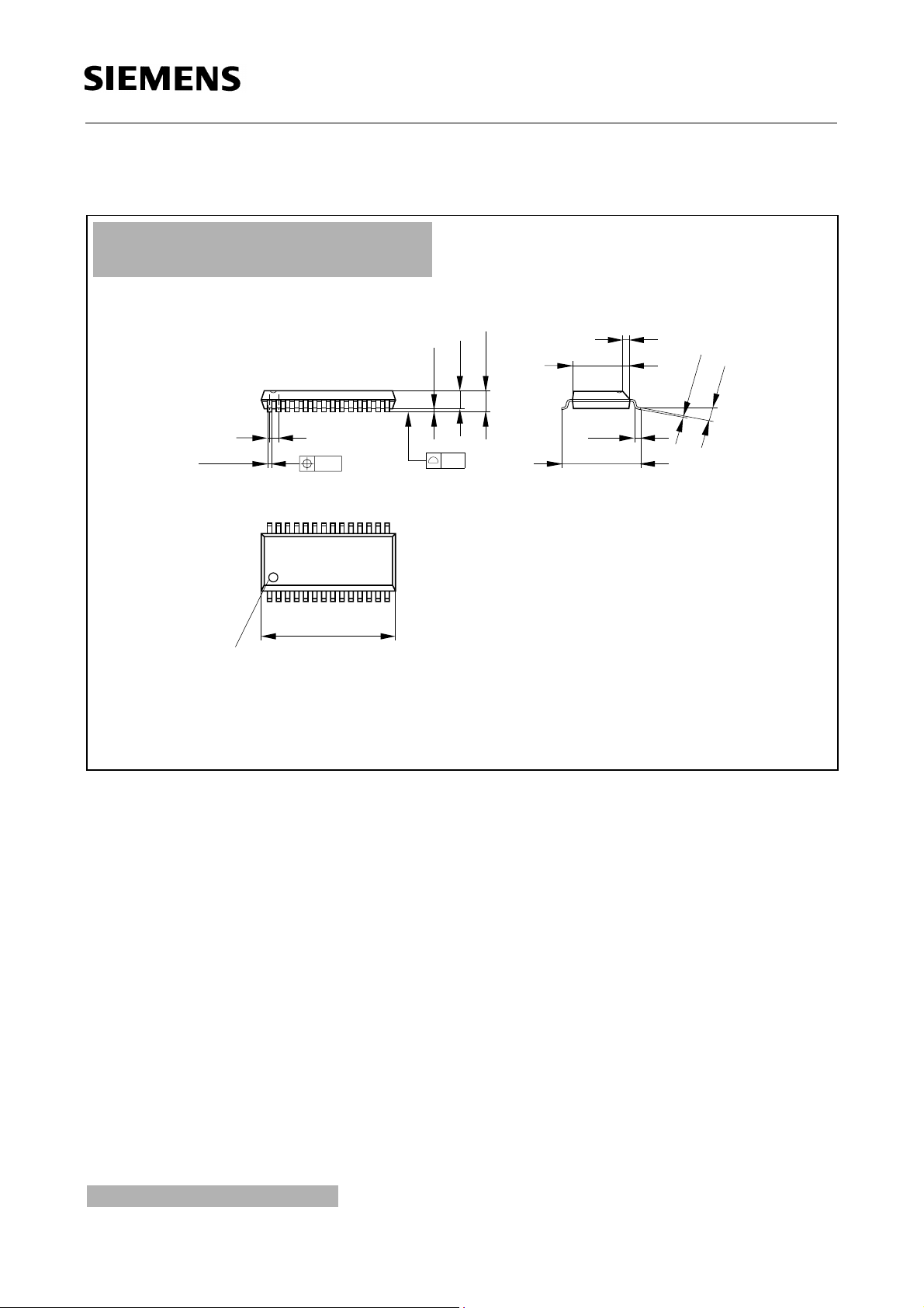
Package Outlines
P-DSO-28-9
(Plastic Dual Small Outline Package)
1.27
+0.15
0.35
2)
0.2 28x
BTS 775 G
0.35 x 45˚
-0.2
-0.1
0.2
2.45
2.65 max
0.1
1528
7.6
10.3
-0.2
0.4
1)
+0.8
±0.3
+0.09
0.23
8˚ max
114
18.1
-0.4
1)
Index Marking
1) Does not include plastic or metal protrusions of 0.15 max rer side
2) Does not include dambar protrusion of 0.05 max per side
GPS05123
Sorts of Packing
Package outlines for tubes, trays etc. are contained in our
Data Book “Package Information”.
SMD = Surface Mounted Device
Dimensions in mm
Semiconductor Group 17 1999-01-07
 Loading...