

Siemens BTS240A Datasheet
TEMPFET
Features
● N channel
● Enhancement mode
● Temperature sensor with thyristor characteristic
● The drain pin is electrically shorted to the tab
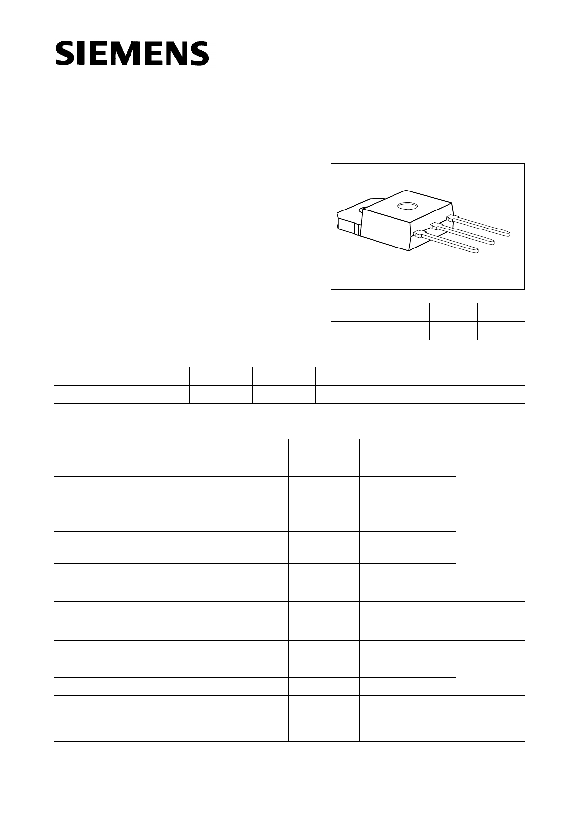
BTS 240A
3
2
1
Pin 1 2 3
GDS
Type
V
DS
I
D
R
DS(on)
Package Ordering Code
BTS 240A 50 V 58 A 0.018 Ω TO-218AA C67078-A5100-A3
Maximum Ratings
Parameter Symbol Values Unit
Drain-source voltage
Drain-gate voltage,
R
= 20 kΩ V
GS
Gate-source voltage
T
Continuous drain current,
= 73 °C I
C
ISO drain current
T
= 85 ˚C, VGS = 10 V, VDS = 0.5 V
C
T
Pulsed drain current,
Short circuit current,
Short circuit dissipation,
= 25 °C I
C
T
= – 55 ... + 150 °C
j
T
= – 55 ... + 150 °C
j
Power dissipation
Operating and storage temperature range
V
DS
DGR
V
GS
D
I
D-ISO
D puls
I
SC
P
SCmax
P
tot
T
j
, T
stg
50 V
50
± 20
58 A
21.0
232
147
2200 W
170
– 55 ... + 150 °C
DIN humidity category, DIN 40 040 – E –
IEC climatic category, DIN IEC 68-1 – 55/150/56
Thermal resistance
Chip-case
Chip-ambient
R
R
th JC
th JA
≤ 0.74
≤ 45
K/W
Semiconductor Group 1 04.97

BTS 240A
Electrical Characteristics
at Tj = 25 °C, unless otherwise specified.
Parameter Symbol Values Unit
min. typ. max.
Static Characteristics
Drain-source breakdown voltage
V
= 0, ID = 0.25 mA
GS
Gate threshold voltage
V
= V
, I
GS
DS
= 1 mA
D
Zero gate voltage drain current
V
= 0 V, VDS = 50 V
GS
T
= 25 °C
j
T
= 125 °C
j
Gate-source leakage current
V
= 20 V, VDS = 0
GS
T
= 25 °C
j
T
= 150 °C
j
Drain-source on-state resistance
V
= 10 V, ID =47 A
GS
Dynamic Characteristics
Forward transconductance
V
≥ 2 × ID× R
DS
DS(on)max
, ID = 47 A
Input capacitance
V
= 0, VDS = 25 V, f = 1 MHz
GS
Output capacitance
V
= 0, VDS = 25 V, f = 1 MHz
GS
Reverse transfer capacitance
V
= 0, VDS = 25 V, f = 1 MHz
GS
Turn-on time
V
= 30 V, VGS = 10 V, ID = 3 A, RGS = 50 Ω
CC
Turn-off time
V
= 30 V, VGS = 10 V, ID = 3 A, RGS = 50 Ω
CC
t
, (ton = t
on
t
, (t
off
off
= t
d(on)
d(off)
+ tr)
+ tf)
V
(BR)DSS
V
GS(th)
I
DSS
I
GSS
R
DS(on)
g
fs
C
iss
C
oss
C
rss
t
d(on)
t
r
t
d(off)
t
f
V
50 – –
2.5 3.0 3.5
µA
–
–
–
–
0.1
10
10
2.0
1.0
100
100
4.0
nA
µA
Ω
– 0.012 0.018
S
20.0 43.0 –
nF
– 2.9 4.3
– 1.4 2.1
– 0.5 0.8
–5075ns
– 150 230
– 350 560
– 250 330
Semiconductor Group 2

BTS 240A
Electrical Characteristics (cont’d)
at Tj = 25 °C, unless otherwise specified.
Parameter Symbol Values Unit
min. typ. max.
Reverse Diode
Continuous source current
Pulsed source current
Diode forward on-voltage
I
= 116 A, VGS = 0
F
Reverse recovery time
I
= IS, diF/dt = 100 A/µs, VR = 30 V
F
Reverse recovery charge
I
= IS, diF/dt = 100 A/µs, VR = 30 V
F
Temperature Sensor
Forward voltage
I
= 10 mA, Tj = – 55 ... + 150 °C
TS(on)
Sensor override, tp≤ 100 µs
T
= – 55 ... + 160 °C
j
Forward current
T
= – 55 ... + 150 °C
j
Sensor override, tp≤ 100 µs
T
= – 55 ... + 160 °C
j
V
Holding current,
= 5 V, Tj = 25 °C
TS(off)
Switching temperature
V
= 5 V
TS
Turn-off time
V
= 5 V, I
TS
TS(on)
= 2 mA
T
= 150 °C
j
I
S
I
SM
V
SD
t
rr
Q
V
TS(on)
I
TS(on)
I
H
T
TS(on)
t
off
– – 58 A
– – 232
V
– 1.6 2.0
ns
– 100 –
rr
µC
– 0.3 –
V
0.7
–
1.4
–
1.5
10
mA
–
–
0.05
0.05
–
–
0.1
0.2
10
600
0.5
0.3
°C
150 – –
µs
0.5 – 2.5
Semiconductor Group 3
 Loading...