

Page 1
XL-S10H
SERVICE MANUAL
No. S2406XLS10H//
MICRO COMPONENT SYSTEM
(Except for U.K.)
CONTENTS
CHAPTER 1. GENERAL DESCRIPTION
[1] SAFETY PRECAUTION FOR SERVICE
MANUAL .......................................................1-1
[2] IMPORTANT SERVICE NOTES (FOR U.K.
ONLY)............................................................1-1
[3] SPECIFICATIONS.........................................1-2
[4] NAMES OF PARTS.......................................1-3
MODEL
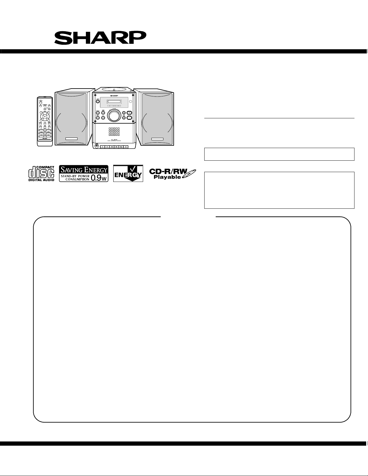
XL-S10H Micro Component System consisting of XLS10H (main unit) and CP-S10H (speaker system).
• In the interests of user-safety the set should be restored to its original condition and only parts identical to those specified be used.
• Note for users in U.K.
Recording and playback of any material may require consent which
SHARP is unable to give. Please refer particularly to the provisions
of Copyright Act 1956, the Dramatic and Musical Performers Protection Act 1956, the Performers Protection Acts 1963 and 1972
and to any subsequent statutory enactments and orders.
CHAPTER 6. CIRCUIT SCHEMATICS AND PARTS
LAYOUT
[1] NOTES ON SCHEMATIC DIAGRAM ............ 6-1
[2] IC701 SERIAL No. TABLE............................. 6-1
[3] TYPES OF TRANSISTOR AND LED ............ 6-1
[4] WIRING SIDE OF P.W.BOARD/SCHE-
MATIC DIAGRAM .......................................... 6-2
XL-S10H
CHAPTER 2. ADJUSTMENTS
[1] ADJUSTMENT ..............................................2-1
[2] TEST MODE .................................................2-2
[3] When the CD does not function ....................2-3
CHAPTER 3. MECHANICAL DESCRIPTION
[1] DISASSEMBLY.............................................3-1
CHAPTER 4. DIAGRAMS
[1] BLOCK DIAGRAM.........................................4-1
CHAPTER 5. CIRCUIT DESCRIPTION
[1] VOLTAGE......................................................5-1
SHARPCORPORATION
CHAPTER 7. OTHERS
[1] FUNCTION TABLE OF IC.............................. 7-1
[2] LCD DISPLAY................................................ 7-3
[3] WIRING OF PRIMARILY SUPPLY LEADS
(FOR U.K. ONLY) .......................................... 7-4
Parts Guide
This document has been published to be used
for after sales service only.
The contents are subject to change without notice.
Page 2
XL-S10H
PROBE
AC
OUT
UNIT
SHORT-CIRCUIT
AC POWER
SUPPLY CORD
CONNECT THE PROBE
TO GND OF CHASSIS
SCREW
WITHSTANDING
VOLTAGE TESTER
AudioXL-S10HService ManualXS10HMarketE
CHAPTER 1. GENERAL DESCRIPTION
[1] SAFETY PRECAUTION FOR SERVICE MANUAL
Precaution to be taken when replacing and servicing the Laser Pickup.
The AEL (Accessible Emission Level) of Laser Power Output for this model is specified to be lower than Class 1 Requirements. However, the following precautions must be observed during servicing to protect your eyes against exposure to the Laser beam.
1) When the cabinet has been removed, the power is turned on without a compact disc, and the Pickup is on a position out er than the lead-in position, the Laser will light for several seconds to detect a disc. Do not look into the Pickup Lens.
2) The Laser Power Output of the Pickup inside the unit and replacement service parts have already been adjusted prior to shipping.
3) No adjustment to the Laser Power should be attempted when replacing or servicing the Pickup.
4) Under no circumstances look directly into the Pickup Lens at any time.
5) CAUTION - Use of controls or adjustments, or performance of procedures other than those specified herein may result in hazardous radiation
exposure.
Laser Diode Properties
Material: GaAIAs
Wavelength: 780 nm
Emission Duration: continuous
Laser Output: max. 0.6 mW
[2] IMPORTANT SERVICE NOTES (FOR U.K.
ONLY)
Before returning the unit to the customer after completion of a repair or
adjustment it is necessary for the following withstand voltage test to be
applied to ensure the unit is safe for the customer to use.
Setting of Withstanding Voltage Tester and set.
Set name set value
Withstanding Voltage Tester
Test voltage 4,240 VPEAK
Set time 6 secs
Set current (Cutoff current) 4 mA
Unit
Judgment
OK: The “GOOD” lamp lights.
NG: The “NG” lamp lights and the buzzer sounds.
ADVERSEL-SYNLIG OG USYNLIG LASERSTRÅLING VED ÅBNING.
SE IKKE IND I STRÅLEN-HELLER IKKE MED OPTISKE INSTRUMENTER.
VARO!AVATTAESSA OLET ALTTIINANÄKYVÄLLE JA NÄKYMÄTTÖMÄLLE
LASERSÄTEILYLLE ÄLÄ TUIJOTA SÄTEESEEN ÄLÄKÄ KATSO SITÄ
OPTISEN LAITTEEN LÄPI.
VARNING-SYNLIG OCH OSYNLIG LASERSTRÅLNING NÄR DENNA
DEL ÄR ÖPPNAD. STIRRA EJ IN I STRÅLEN OCH BETRAKTA EJ
STRÅLEN GENOM OPTISKT INSTRUMENT.
VAROITUS! LAITTEEN KÄYTTÄMINEN MUULLA KUIN TÄSSÄ
KÄYTTÖOHJEESSA MAINITULLA TAVALLA SAATTAA
ALTISTAA KÄYTTÄJÄN TURVALLISUUSLUOKAN 1
YLITTÄVÄLLE NÄKYMÄTTÖMÄLLE LASERSÄTEILYLLE.
VARNING - OM APPARATEN ANVÄNDS PÅ ANNAT SÄTT ÄN
I DENNA BRUKSANVISNING SPECIFICERAS. KAN
ANVÄNDAREN UTSÄTTAS FÖR OSYNLIG LASERSTRÅLNING, SOM ÖVERSKRIDER GRÄNSEN FÖR
LASERKLASS 1.
3,000 VRMS
1 – 1
Page 3
FOR A COMPLETE DESCRIPTION OF THE OPERATION OF THIS UNIT, PLEASE REFER
TO THE OPERATION MANUAL.
[3] SPECIFICATIONS
Except for U.K.
XL-S10H
■ General
Power source AC 230 V, 50 Hz
Power consumption Power on: 25 W
Power stand-by: 0.9 W
Dimensions Width: 160 mm (6-5/16")
Weight 2.3 kg (5.1 lbs.)
Height: 242 mm (9-1/2")
Depth: 250 mm (9-7/8")
■ Amplifier
Output power PMPO: 30 W (total)
MPO: 15 W (7.5 W + 7.5 W) (DIN 45 324)
RMS: 10 W (5 W + 5 W) (DIN 45 324)
Output terminals Speakers: 4 ohms
Headphones: 16 - 50 ohms
(recommended: 32 ohms)
■ Tuner
Frequency range FM: 87.5 - 108 MHz
AM: 522 - 1,620 kHz
For U.K.
■ CD pl ayer
Type Compact disc player
Signal readout Non-contact, 3-beam semiconductor laser
D/A converter 1-bit D/A converter
Frequency response 20 - 20,000 Hz
Dynamic range 90 dB (1 kHz)
pickup
■ Cassette deck
Frequency response 125 - 8,000 Hz (normal tape)
Signal/noise ratio 50 dB (recording/playback)
Wow and flutter 0.35 % (DIN 45 511)
■ Speaker
Type 10 cm (4") full-range speaker
Maximum input
power
Rated input power 5W
Impedance 4 ohms
Dimensions Width: 130 mm (5-1/8")
Weight 1.4 kg (3.1 lbs.)/each
10 W
Height: 240 mm (9-7/16")
Depth: 161 mm (6-5/16")
■ General
Power source AC 230 - 240 V, 50 Hz
Power consumption
Dimensions Width: 160 mm (6-5/16")
Weight 2.3 kg (5.1 lbs.)
Power on: 25 W
Power stand-by: 0.9 W
Height: 242 mm (9-1/2")
Depth: 250 mm (9-7/8")
■ Amplifier
Output power RMS: 10 W (5 W + 5 W) (10 % T.H.D.)
Output terminals Speakers: 4 ohms
Headphones: 16 - 50 ohms
(recommended: 32 ohms)
■ Tun e r
Frequency range FM: 87.5 - 108 MHz
AM: 522 - 1,620 kHz
■ CD player
Type Compact disc player
Signal readout Non-contact, 3-beam semiconductor laser
D/A converter 1-bit D/A converter
Frequency
response
Dynamic range 90 dB (1 kHz)
pickup
20 - 20,000 Hz
■ Cassette deck
Frequency
response
Signal/noise ratio 50 dB (recording/playback)
Wow and flutter 0.3 % (WRMS)
125 - 8,000 Hz (normal tape)
■ Speaker
Type 10 cm (4") full-range speaker
Maximum input
power
Rated input power 5W
Impedance 4 ohms
Dimensions Width: 130 mm (5-1/8")
Weight 1.4 kg (3.1 lbs.)/each
10 W
Height: 240 mm (9-7/16")
Depth: 161 mm (6-5/16")
Specifications for this model are subject to change without prior
notice.
1 – 2
Page 4
XL-S10H
[4] NAMES OF PARTS
22
23
1
2
3
4
5
6
7
8
15 16 17 18 19 20 21
28
29
9
10
11
12
13
14
24
25
26
32
3127 30
33
34
35
1. CD Compartment
2. On/Stand-by Button
3. Volume Control
4. Bass/Treble Selector Button
5. Function Selector Button
6. Memory/Set Button
7. Clear Button
8. Cassette Compartment
9. CD Eject Button
10. Remo te Sensor
11. CD Track Up or Fast Forward,
Tuner Preset Up Button
12.CDPlayorPause,TuningUpButton
13. CD Stop, Tuning Down Button
14. CD Track Down or Fast Reverse,
Tuner Preset Down Button
15. Head p hone Socket
16. Tape Record Button
17. Tape Play Button
18. Tape Rewind Button
19. Tape Fast Forward Button
20. Tape Stop/Eject Button
21. Tape Pause Bu tto n
22. Volume Indicator
23. Equaliser Indicator
24. Sleep Indicator
25. Tape Record I ndi cato r
26. T ime r Play Indicator
27. CD Repeat Play Indicator
28. CD Play Indicator
29. CD Random Play Indicator
30. Memory Indicator
31. FM Stereo Mode Indicator
32. F M Stereo Receiving Indicator
33. F M/AM Loop Aerial Socket
34. Sp eaker Terminals
35. AC Power Lead
10
11
12
13
14
15
1. F ull-Range Speaker
2. Speaker Wire
1
Note:
The speaker grilles are not removable.
2
3
4
5
6
7
8
16
17
18
19
20
9
21
22
23
3. Remote Control Transmitter
4. On/Stand-by Button
5. CD Button
6. CD Fast Reverse, Tuning Down Button
7. CD Track D own, Tuner Preset Down Button
8. CD Play Button
9. CD Stop Button
10. M emory Button
11. Clear Button
12. Clock Button
13. Treble Up and Down Buttons
14. Bass Up and Down Buttons
15. Volume Up and Down Buttons
16. Tuner and Band Selector Button
17. Tape Button
18.CDFastForward,TuningUpButton
19. CD Track Up, Tuner Preset Up Button
20. CD Pause Button
21. Random/Repeat Button
22. T im er Button
23. S leep Button
1 – 3
Page 5
AudioXL-S10HService ManualXS10HMarketE
CHAPTER 2. ADJUSTMENTS
XL-S10H
• FM Mute Level
Signal generator: 1 kHz, 40 kHz dev., FM modulated
[1] ADJUSTMENT
1. MECHANISM SECTION
• Driving Force Check
Torque Meter Specified Value
Play: TW-2111 Over 80 g
• Torque Check
Torque Meter Specified Value
Play: TW-2111 30 to 80 g.cm
Fast forward: TW-2231 70 to 180 g.cm
Rewind: TW-2231 70 to 180 g.cm
• Tape Speed
Test Tape Adjusting
Point
MTT-111 Variable
Resistor in
motor.
TAPE MECHANISM
Specified
Value
3,000 ± 30 Hz Speaker Ter-
Instrument
Connection
minal (Load
resistance: 6
ohms)
VARIABLE RESISTOR
IN MOTOR
Frequency Display Adjusting
Parts
98.00 MHz
98.00 MHz Input: Antenna
(30 dBµV)
Instrument
Connection
Output: Speaker Terminal
• FM Detection
Signal generator: 10.7 MHz FM sweep generator
Test
Stage
Frequency Frequency
Display
Setting/
Adjusting
Instrument
Connection
Parts
FM IF 10.7 MHz 98.00 MHz Input: Pin 36 of
IC301
Output: Pin 23
of IC301
• FM RF
Signal generator: 1 kHz, 75 kHz dev., FM modulated
Test
Stage
Frequency Frequency
Display
Setting/
Adjusting
Instrument
Connection
Parts
FM Band
Coverage
FM RF 98.00 MHz
— 87.50 MHz (fL): L307
1.5 ± 0.1 V
98.00 MHz L304 *1
*1
(10 ~ 20dB)
*1. Input: Antenna Output: 23 Pin of IC301
MAIN PWB-A1
Figure 1
2. TUNER SECTION
fL: Low-range frequency
fH: High-range frequency
• AM IF/RF
Signal generator: 400 Hz, 30%, AM modulated
Test Stage Frequency Frequency
Display
Setting/
Adjusting
Parts
IF 450 kHz 1,602 kHz L305 *1
AM Band
Coverage
— 522 kHz (fL): L306
1.1 ± 0.1 V
AM Tracking 990 kHz 990 kHz L302 *3
*1. Input: IC301 1Pin Output: IC301 23Pin
*2. Input: Input is not connected Output: TP-VT(IC301 28Pin)
*3. Input: Antenna Output:IC301 23Pin
• Check FM VT
Signal generator: 1 kHz, 40 kHz dev., FM modulated
Frequency Display Check
Point
Instrument
Connection
87.5 MHz 87.5 MHz 1.5V ± 1.0V TP-VT
108 MHz 108 MHz 5.0V ± 1.0V TP-VT
Instrument
Connection
*2
FM OSC.
L307
FM BAND
COVERAGE fL
IC301
TP-VT=28Pin
L305
AM IF
L304
FM RF
AM ANT.
L306
L302
AM
Tracking
AM BAND
COVERAGE fL
Figure 2 ADJUSTMENT POINTS
3. CD SECTION
• Adjustment
Since this CD system incorporates the following automatic adjust-
ment functions, readjustment is not needed when replacing the
pickup. Therefore, different PWBs and pickups can be combined
freely.
Each time a disc is changed, these adjustments are performed
automatically. Therefore, playback of each disc can be performed
under optimum conditions.
CNP301
2 – 1
Page 6
XL-S10H
[2] TEST MODE
Test Mode Key Operation
KEY1 KEY2 KEY3 TEST CONTENTS INDICATION
Memory Preset Down Power Preset clear Tu CL
Memory Stop Power Preset set FM P-01
Memory Play Power Display
Memory Preset up Power CD T-1
Memory Clear Power Soft reset CL
Bass/treble Preset down Power Volume T-3
Bass/treble Play Power Timer test T-4
Bass/treble Clear Power all key T-6
September 12 Days Indication Change
All test modes can be terminated by turning off the power with POWER key.
• Preset clear test
All tuner preset stations are cleared.
• Preset set test
CH BAND FREQUENCY
1 FM STEREO FM 87.50 MHz
2 FM 108.00 MHz
3 FM 98.00 MHz
4 FM 90.00 MHz
5 FM 106.00 MHz
6 AM AM 522 kHz
7 AM 1620 kHz
8 AM 990 kHz
9 AM 603 kHz
CH BAND FREQUENCY
10 AM AM 1404 kHz
11 ——————
·
·
35
36 FM MONO FM 106.00 MHz
37 FM 90.00 MHz
38 FM 98.00 MHz
39 FM 108.00 MHz
40 FM 87.50 MHz
Stations are set according to destination.
• Display test
When test mode is activated, the entire display lights up. As the “PLAY” button is pressed, half of the display lights up alternately .
• CD test
[cd step 1] Enter test mode.
↓ Hold down the “memory” button
[cd step 2] After some steps, the laser turns on.
↓ Hold down the “memory” button
[cd step 3] After some steps, focus search is performed.
↓ Hold down the “memory” button
[cd step 4] After some steps, CLV rotation is performed.
↓ Hold down the “memory” button
[cd step 5] CD playback starts.
↓ Hold down the “stop” button to return to [cd step 1] ––––––––––
In step 5, hold down the AUX button on the remote control. The tracking servo is switched on/off.
From step 3, the pick up can be moved with the FF/REW button.
• So ft reset test
All data in RAM is cleared.
• VOLUME test
Starting from level 23 (default), check all the levels (0 - 23 - MAX).
• TIMER test
Start the timer at 1:00. When it reaches 1:05, turn on the power with the AUX function and turn off the power after about 30 seconds.
(In the test mode, fade-in and fade-out are not required.)
• A LL KEY test
In the test mode, hold down all the buttons on the main unit and then press the “POWER” button. “OK” appears.
If only the “POWER” key is pressed, “ERROR” appears.
←———————
2 – 2
Page 7
XL-S10H
[3] When the CD does not function
The CD section may not operate when the objective lens of the optical pickup is dirty. Clean the objective lens, and check the playback operation.
When this section does not operate even after the above step is taken, check the following items.
Turn the power off.
Gently clean the lens with a lens cleaning tissue and a small amount of isopropyl alcohol.
Do not touch the lens with the bare hand.
Parts code
1. CD optical pickup Lens cleaner disc UDSKA0004AFZZ
HOW TO USE
1. Using the brush in the cleaner cap, apply 1 or 2 drops of the cleaning fluid to the brush on the CD cleaner disc which has
mark next to it.
the
2. Place the CD cleaner disc onto the CD disc tray with the brush side down, then press the play button.
3. You will hear music for about 20 seconds and the CD player will automatically stop. If it continues to turn, press the stop
button.
CAUTION
The CD lens cleaner should be effective for 30~50 operations, however if the brushes become worn out earller then please
replace the cleaner disc.
If the CD cleaner brushes become very wet then wipe off any excess fluid with a soft cloth.
Do not drink the cleaner fluid or allow it to come in contact with the eyes. In the event of this happening then drink and /
or rinse with clean water and seek medical advice.
The CD cleaner disc must not be used on car CD players or on computer CD ROM drives.
All rights reserved. Unauthorized duplicating, broadcasting and renting this product is prohibited by law.
Cleaner Liquid
Cleaning Disc
PARTS CODE: UDSKA0004AFZZ
2 – 3
Page 8
XL-S10H
(A3)x1
(A2)x2
Top Cabinet
Open/Close
Switch PWB
CD Mechanism
Side Panel
(Right)
Rear Panel
(C1)x2
ø3x10mm
Side Panel
(Lift)
(A1)x1
ø3x10mm
(A1)x2
ø3x10mm
(A1)x1
ø3x10mm
(A1)x1
ø3x10mm
(B1)x2
ø3x10mm
(B1)x2
ø3x10mm
Top Cabinet
AudioXL-S10HService ManualXS10HMarketE
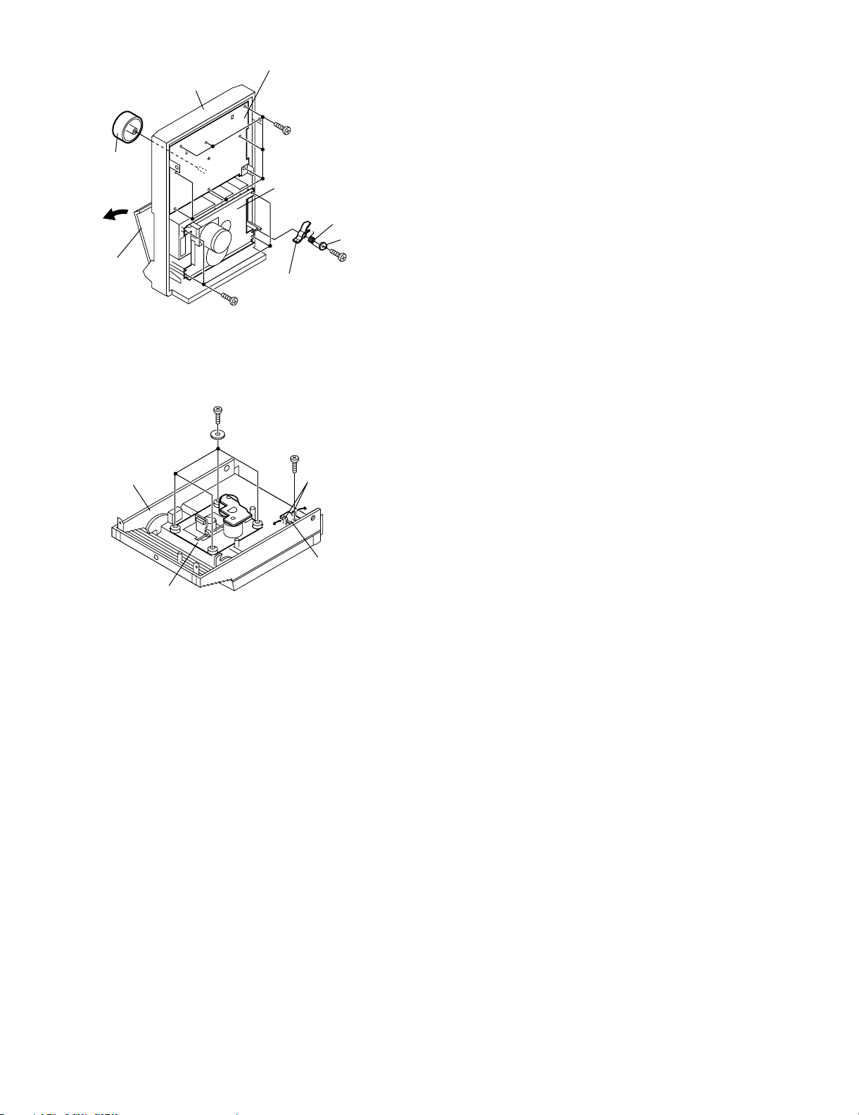
CHAPTER 3. MECHANICAL DESCRIPTION
[1] DISASSEMBLY
Caution on Disassembly
Follow the below-mentioned notes when disassembling the unit and
reassembling it, to keep it safe and ensure excellent performance:
1) Take cassette tape and compact disc out of the unit.
2) Be sure to remove the power supply plug from the wall outlet
before starting to disassemble the unit.
3) Take off nylon bands or wire holders where they need to be
removed when disassembling the unit. After servicing the unit,
be sure to rearrange the leads where they were before disassembling.
4) Take sufficient care on static electricity of integrated circuits and
other circuits when servicing.
STEP REMOVAL PROCEDURE FIGURE
1 Top Cabinet 1. Screw...........................(A1) x 5
2. Socket.........................(A2) x 2
3. Flat Cable....................(A3) x 1
2 Side Panel 1. Screw...........................(B1) x 4 1
3 Rear Panel 1. Screw..........................(C1) x 2
2. Screw..........................(C2) x 2
4 Main PWB 1. Screw..........................(D1) x 2
2. Socket.........................(D2) x 2
3. Socket.........................(D3) x 1
5 Front Panel 1. Screw...........................(E1) x 2 3
6 Power PWB 1. Screw...........................(F1) x 2
2. Screw...........................(F2) x 1
7 Display PWB 1. Knob............................(G1) x 1
2. Screw..........................(G2) x 8
8 Tape Mechanism 1. Screw..........................(H1) x 1
2. Screw..........................(H2) x 4
9 Open/Close
Switch PWB
10 CD Mechanism 1. Screw...........................(K1) x 4 5
Note 1:
After removing the connector for the optical pickup from the connector,
wrap the conductive aluminium foil around the front end of the connector so as to protect the optical pickup from electrostatic damage.
1. Screw...........................(J1) x 1
2. Hook............................(J2) x 2
1
1
2
2
3
4
4
5
Top Cabinet
Figure 1
(D3)x1
(D1)x2
ø3x10mm
(D2)x1
(C2)x2
ø3x10mm
Main PWB
3 – 1
(D2)x1
Front Panel
(E1)x2
ø3x10mm
Power PWB
Figure 2
(F1)x2
ø3x10mm
(F2)x1
ø3x10mm
PWB
AC cord
Power
PWB
Figure 3
Page 9
(G1)x1
Open
XL-S10H
Display PWB
Front Panel
(G2)x8
ø2.6x10mm
Tape
Mechanism
Spring
PWB
Cassette
Holder
Top Cabinet
CD Mechanism
(H2)x4
ø3x10mm
Figure 4
(K1)x4
ø2.6x10mm
Figure 5
Lever
(J1)x1
ø2.6x10mm
(J2)x2
(H1)x1
ø2.6x10mm
Open/Close
Switch PWB
3 – 2
Page 10
XL-S10H
M
T
A
AudioXL-S10HService ManualXS10HMarketE
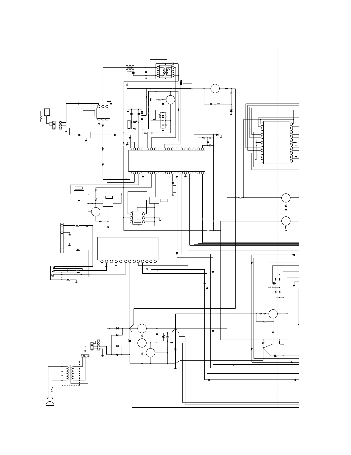
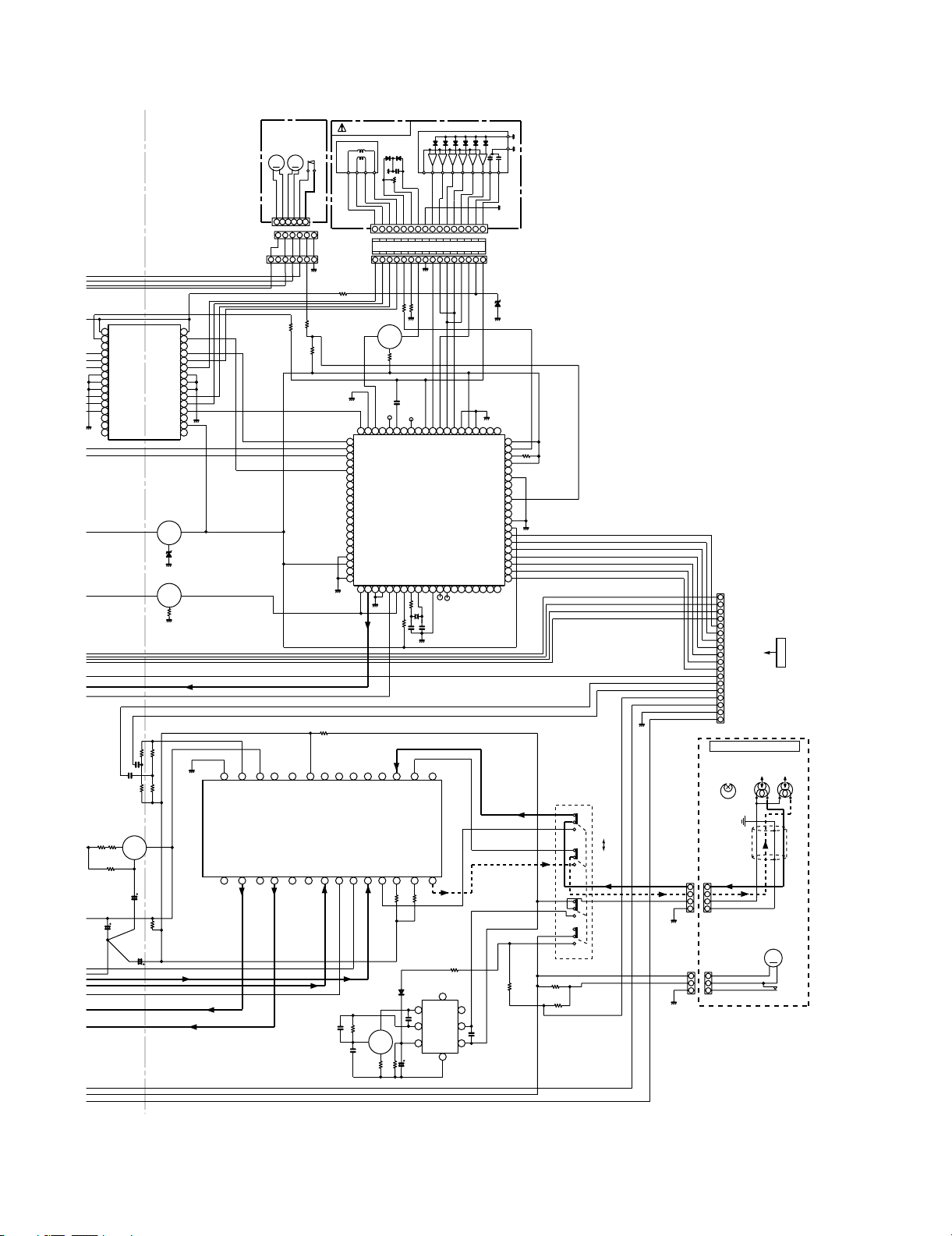
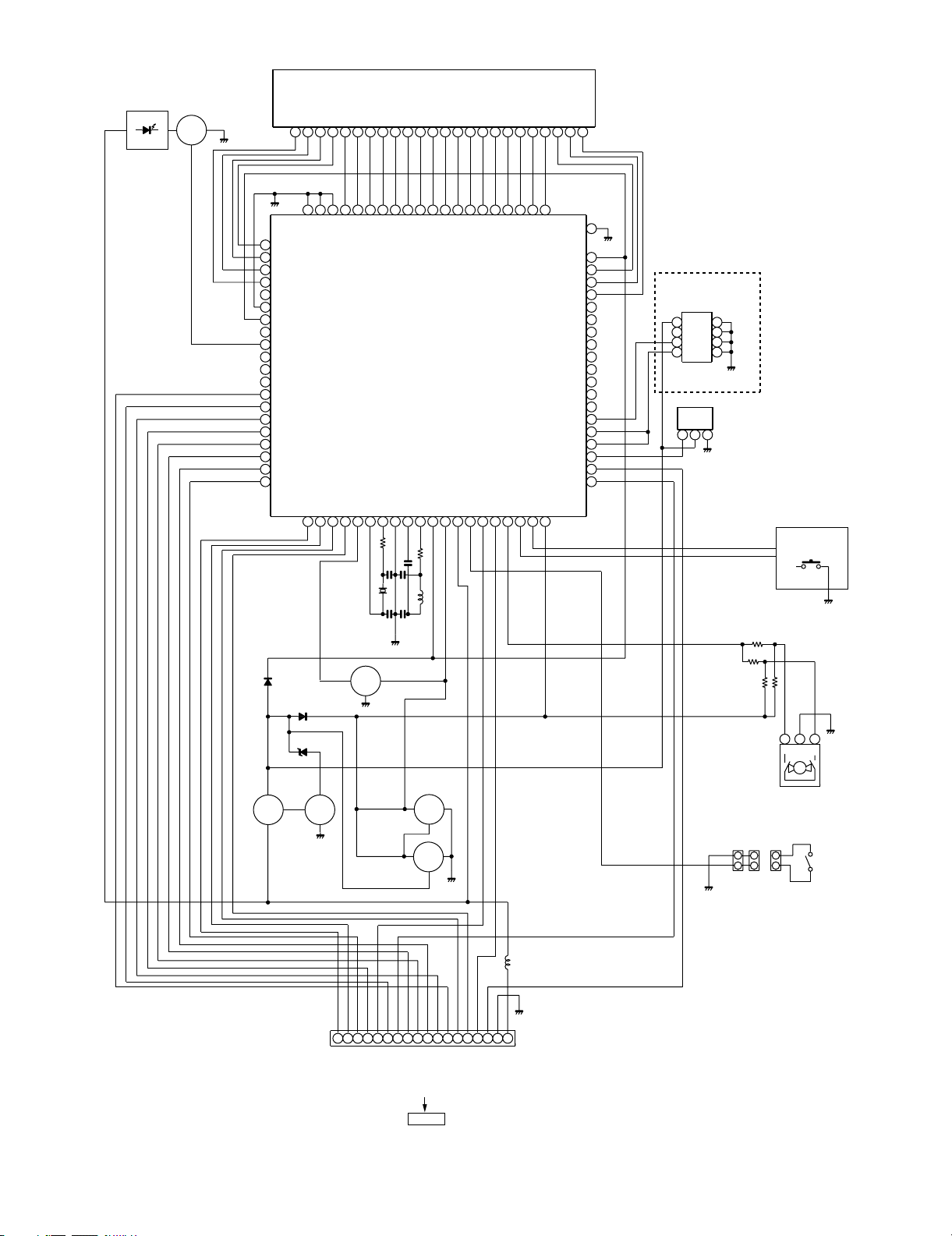
CHAPTER 4. DIAGRAMS
[1] BLOCK DIAGRAM
AM BAND
COVERAGE fL
D305
+B
AM OSC
L306
AM:1V-8V
4
5
6
FM:1.5V-5.0V
TP-VT
VTCC
CONSTANT
VOLTAGE
Q301
VP
3
2
1
FM OSC
B02
AM-OSC
FMRF-IN
VCC1
123457612 10 9 81113
L307
D307
B01
P-DET
AM IF
Q302
LP-OUT
P-DET
LP-IN
P-CCMP
CF302
PD
FM-IET
FM IF
AGC
AMLOWOUT
R-OUT
L-OUT
222324252627282930
MPX-IN
DET-OUT
CE
VSS
X301
75KHz
19202136 35 34
XIN
VDD
XOUT
D0
CL
DI
AMP_A1_ON
D308
IC301
LV23002M
FM FRONT END
D309
PLL(TUNER)
FM IF DET./FM MPX./AM IF
VCCVCC
30
REF-IN
29
1-SPD
28
G-SPD
27
0+SPD
26
0-SPD
25
GND
24
GND
23
GND
22
0-SLD
21
IC802
0+SLD
20
G-SLD
19
1-SLD
18
TCAP
17
16 15
CD_A1_VCC
REG-OUT
RESET REG-TR
FOCUS/TRACKING/
SPIN/SLED DRIVER
CONSTANT
1
MUTE
2
1-FCS
3
G-FCS
4
0+FCS
5
0-FCS
6
GND
7
GND
8
GND
9
0-TRK
10
0+TRK
11
LA6548D
G-TRK
12
I-TRK
13
14
VOLTAGE
Q802
D802
Q801
CONS
VOLT
AM LOOP
ANTENNA
CNP301
1
1
2
2
3
L-CH
SPEAKER
TERMINAL
R-CH
J103
HEADPHOMES
3
+
–
–
+
J101
ANTENNA
BAND PASS
FM IF
CF301
AM
Tracking
FILTER
CF306
Q371
321
L302
AM ANT.
4
5
FM IF
CF304
(L)
(R)
6
POWER AMP.
D306
L304
FM RF
33 32 31
VCC2
FMRF-OUT
FM-OSC
FMRF-IN
AM-MIX
GND1
FM-MIX
REG
AMRF-IN
123 1817164 5 6 7 8 9 10 11 12 13 14 15
CF303
3
4
2
5
L305
AM IF
1
6
IC101
LA4631++
F653
TRANSFORMER
T315mA L 250V
AC POWER
SUPPLY CORD
AC 230 V, 50 Hz
CNP101
PT1
POWER
123
CNS101
1
2
3
1
2
3
4
CNW101
D104
D102
D101
D103
MA-VCC
Q101
Q102
D106
Q103
CD_A1_VCC
TP-VM
P-ON
Figure 4-1 BLOCK DIAGRAM (1/3)
4 – 1
CONSTANT
VOLTAGE
Q502
Page 11
VCCVCC
30
REF-IN
29
1-SPD
28
G-SPD
27
0+SPD
26
0-SPD
25
GND
24
GND
23
GND
22
0-SLD
21
IC802
0+SLD
20
G-SLD
19
1-SLD
18
17
16 15
REG-OUT
TCAP
RESET REG-TR
FOCUS/TRACKING/
SPIN/SLED DRIVER
CONSTANT
CD_A1_VCC
CONSTANT
VOLTAGE
Q502
1
MUTE
2
1-FCS
3
G-FCS
4
0+FCS
5
0-FCS
6
GND
7
GND
8
GND
9
0-TRK
10
0+TRK
11
LA6548D
G-TRK
12
I-TRK
13
14
VOLTAGE
Q802
D802
CONSTANT
Q801
VOLTAGE
SLED
SPINDLE
MOTOR
MOTOR
PICKUP IN
M
M
+
+
–
–
SP+
SP–
SL+
SL–
PU-IN
1234
1234
514623
5
CNS802
CNW802
+B
13 12 11 10 9 8 7 6 514
SD
VCC
GND
BB2
5
1
TRE2
TRE1
BD3881FV
RECORD/PLAYBACK AMP.
A1
OUT1
BB1
OUT2
9
6
1
1
1
8
1
7
GND
6
5
6
7
+B
VCC2
IC201
A2
2
0
VOL2
B1
2
1
CD PICKUP UNIT
FO+
MD
TR+
TR-
FO-
ACTUATOR
VR
TR-
FO-
TR+
FO+
MD(PD)
16151413121110987654321
13141516 12 11 10 123456789
LASER
DRIVER
Q803
RFMON
TDO
ADAVSS
FDO
2
TE
1
SPDO
2
2
JITTC
SLDO
32
24
2
5
62
7
2
2
8
2
9
3
0
3
1
2
3
3
3
4
3
3
5
3
6
7
3
3
8
3
9
40
VOL1
B2
2
2
GPDAC
CONT4
CONT5
SBCK/FG
DEFECT
V/1P
FSEQ
MON11
MON12
MON13
MON14
MON15
VSS
VDD
DOUT
TEST
LCHO
2
4
1
4
LVDD
SEL-OUT1
SEL-OUT2
C2
C1
24
32
ADAVDD
LVSS
3
4
44
2
RFMON
CD SERVO
RVSS
RCHO
RVDD
7
4
4
5
6
4
43 2 1
PB2P
PB2N
REC2N
REC20
62
5
+++++----
LD
FBA
F
C
LD
VR
GND
CFW801
FE
FE
TEC
REF1
VREF
TIN2F
TIN1E
IC801
LC78646E
XVDD
XOUT
XIN
FSX/16MIN
XVSS
C2F
9
1
2
4
5
5
0
5
8
4
X801
16.9344MHz
PB1P
PB1N
REC10
REC1N
7
2
2
8
C
BAE
FIN2B
FIN1A
EFLG
IGMOUT
535
4
TP8
D
RSVSS
ASRACK
557
5
5
-
D
+5V
4567891011121314151617
RF
RFVDD
PCKIST
ASDFIN
ASDACK
6
5
-
+
E
1/2V
CNS801
EFMIN
VVDD
VVSS
PD02
PD01
CONT2
CONT3
VSS
VDD5
DRF
VRES
VWRQ
LRSY
59
8
VC
VCC
GND
D801
1232019 18
SLCO
FR
SLCIST
68
67
DO
DI
CL
CE
DATA
DATACK
0
6
80
79
78
77
76
75
74
73
72
71
70
69
66
65
64
63
62
61
1/2VCC
LDD
LDS
XL-S10H
CNP503
1
1-TU-SDI
2
0-TU-SCK
3
0-TU-SDO
4
0-TU-CE
5
I-CD-DRF
6
0-CD-/RESET
7
I-CD-WRQ
8
1-CD-DATA
9
O-CD-CMD
10
0-CD-CLK
11
0-CD-CE
12
0-AMP-ON
13
0-EVR-SD0
14
0-EVRCLK
15
1-TP-STATE
16
0-POWER
17
D-GND
18
VP
TAPE MECHANISM ASS'Y
ERASE HERD
C
S501
P.B.
REC.
B
CNP501
CNA501
4
4
3
3
2
A
2
1
1
CNS701
FROM DISPLAY PWB
RECORD/PLAYBACK
HEAD
R-CH
L-CH
TP-VM
8
1
6
2
5
Q503
L501
4
3
7
Figure 4-2 BLOCK DIAGRAM (2/3)
4 – 2
D
M501
TAPE
M
CNA502
3
2
1
MOTOR
SW501
PLAY
CNP502
3
2
1
Page 12
XL-S10H
LED701~704
Q703
LCD701
FL DISPLAY
S19
S18
S17
S16
S15
S14
S13
S12
S11
S10
S9
S8
S7
S6
S5
S4
S3
S2
S1
S0
C3
C2
C1
C0
60 59 58 57 56 55 54 53 52 51 50 49 48 47 46 45 44 43 42 41
S39
S38
S37
S36
S35
S34
S33
S32
S31
S30
S29
S28
S27
S26
V1/PL4
V2/PL5
61
COM0
62
COM1
63
COM2
64
COM3
65
PWM2
66
VSS3
+B
67
VDD3
68
PWM3
69
P00
70
P01
71
P02
72
P03
73
P04
74
P05
75
P06
76
P07
P10/S00
77
P11/S10
78
P12/SC0
79
P13/S01
80
V3/PL6
IXA006SJ
IXA007SJ
IXA019SJ
SYSTEM
MICROCOMPUTER
NOTE:
Serial No.table (See 6-1)
IC701
S25
P73/INT3/TOIN
S24
VSS2
S15
VDD2
S7/PA7
S6/PA6
S5/PA5
S4/PA4
S3/PA3
S2/PA2
S1/PA1
S0/PA0
P72/INT2
P71/AN9
S14
S13
S12
S11
S10
242322212019181716151413121110987654321
40
39
38
37
36
35
34
33
S9
32
31
S8
30
29
28
27
26
25
24
23
22
21
IC701
IC7A1
8
7
6
5
AT24C16
OUT
: IXA007SJ
1
2
3
4
RX701
REMOTE
VCC
GND
SENSOR
321
P15/SC1
P14/SI1
Q704Q702
P16
P17
RESET
Q706
XT2/AN11
XT1/AN10
32.768KHz
X702
VSS1
RESET
CF1
CF2
Q705
Q701
L701
VDD1
P81/AN1
P80/AN0
P83/AN3
P82/AN2
P85/AN5
P84/AN4
P87/AN7
P86/AN6
2019181716151413121110987654321
P70/AN8
CNW702
2
121
CNS702
CNP702
2
1
SW702~705
SW707~711
21
SW700
VOLUME
SW701
CD LID
3
987654321
I-TU-SDI
O-TU-CE
O-TU-SCK
O-TU-SDO
1-CD-DRF
O-CD-/RESET
I-CD-WRQ
I-CD-DATA
O-CD-CMD
O-CD-CE
O-CD-CLK
O-AMP-ON
O-POWER
I-TP-STATE
O-EVR-SCK
O-EVR-SDO
CNP503
TO MAIN PWB
Figure 4-3 BLOCK DIAGRAM (3/3)
4 – 3
+B
181716151413121110
VP
D-GND
L702
CNS701
Page 13
AudioXL-S10HService ManualXS10HMarketE
CHAPTER 5. CIRCUIT DESCRIPTION
[1] VOLTAGE
XL-S10H
PIN
NO.
10
11
12
13
PIN
NO.
10
11
12
13
14
15
16
17
18
19
20
21
22
23
24
25
26
27
28
1
2
3
4
5
6
7
8
9
1
2
3
4
5
6
7
8
9
IC101
VOLTAGE
8.8 V
1.5 V
0V
1.5 V
-1.3 V
11.5 V
17.7 V
0V
0V
0V
0V
8.4 V
0V
IC201
VOLTAGE
3.66 V
3.68 V
3.65 V
3.65 V
3.65 V
3.65 V
3.65 V
3.65 V
3.65 V
3.65 V
3.65 V
7.55 V
3.65 V
0V
3.65 V
3.65 V
3.65 V
3.65 V
3.65 V
3.65 V
3.65 V
3.65 V
3.65 V
3.65 V
3.65 V
3.65 V
3.65 V
3.65 V
PIN
NO.
10
11
12
13
14
15
16
17
18
19
20
21
22
23
24
25
26
27
28
29
30
31
32
33
34
35
36
PIN
NO.
1
2
3
4
5
6
7
8
9
1
2
3
4
5
6
7
8
9
10
11
12
13
14
15
16
17
18
19
20
21
22
23
24
25
26
27
28
29
30
IC301
VOLTAGE
2.25 V
2.28 V
2.59 V
0V
5.08 V
2.23 V
2.25 V
4.0 V
3.9 V
2.9 V
2.43 V
2.43 V
0V
0V
0V
0V
0V
0V
1.82 V
1.67 V
3.9 V
2.24 V
0.69 V
2.57 V
2.1 V
2.5 V
2.0V
3.1 V
2.7 V
2.1 V
4.9 V
5.1 V
4.9 V
5.1 V
0V
0.97 V
IC802
VOLTAGE
8.46 V
3.19 V
1.60 V
1.61 V
3.87 V
2.75 V
0V
0V
0V
3.72 V
3.70 V
1.60 V
1.60 V
3.22 V
7.39 V
3.21 V
3.83 V
1.60 V
1.60 V
3.91 V
3.80 V
0V
0V
0V
3.53 V
4.11 V
1.61 V
1.60 V
1.61 V
8.44 V
PIN
NO.
10
11
12
13
14
15
16
17
18
19
20
21
22
23
24
25
26
27
28
29
30
31
32
33
34
35
36
37
38
39
40
41
42
43
44
45
46
47
48
49
50
51
52
53
54
55
56
57
58
59
60
61
62
63
64
65
66
67
68
69
70
71
72
73
74
75
76
77
78
79
80
1
2
3
4
5
6
7
8
9
IC701
VOLTAGE
4.45 V
0V
0V
0V
4.42 V
2.126 V
2.710 V
0V
2.305 V
2.637 V
5.19 V
5.26 V
1.324 V
0.115 V
3.205 V
2.021 V
5.56 V
5.19 V
5.13 V
0V
0V
4.97 V
5.11 V
0V
0V
0V
0V
0V
5.10 V
0V
0V
0V
0V
0V
0V
0V
0V
0V
0V
5.11 V
2.33 V
2.324 V
2.03 V
2.26 V
2.38 V
2.50 V
2.50 V
2.50 V
2.50 V
2.50 V
2.50 V
2.50 V
2.50 V
2.44 V
2.37 V
2.44 V
2.32 V
2.38 V
0V
0V
2.48 V
2.48 V
2.47 V
2.48 V
1.63 V
0V
1.0 V
2.13 V
5.0 V
0V
0V
0V
4.96 V
5.0 V
0.7 V
0V
1.12 V
3.4 V
0.7 V
0V
PIN
NO.
10
11
12
13
14
15
16
17
18
19
20
21
22
23
24
25
26
27
28
29
30
31
32
33
34
35
36
37
38
39
40
41
42
43
44
45
46
47
48
49
50
51
52
53
54
55
56
57
58
59
60
61
62
63
64
65
66
67
68
69
70
71
72
73
74
75
76
77
78
79
80
1
2
3
4
5
6
7
8
9
IC801
VOLTAGE
1.6 V
1.0 V
1.6 V
1.67 V
3.2 V
0V
1.6 V
1.6 V
1.6 V
1.6 V
1.6 V
1.6 V
1.6 V
1.7 V
1.58 V
1.6 V
1.57 V
3.2 V
0V
1.6 V
1.6 V
1.6 V
1.6 V
1.6 V
1.6 V
1.5 V
0V
1.5 V
0V
0V
1.0 V
0V
0V
0V
1.5 V
1.5 V
0V
3.2 V
3.2 V
0V
3.5 V
1.7 V
0V
0V
1.75 V
3.8 V
3.1 V
1.4 V
1.6 V
1.5 V
0V
0V
1.25 V
1.25 V
1.52 V
1.52 V
1.58 V
1.58 V
1.0 V
0V
0.18 V
3.0 V
1.9 V
3.0 V
3.9 V
3.3 V
0V
3.2 V
0V
0V
0V
3.1 V
0.54 V
1.35 V
0V
1.0 V
3.26 V
2.5 V
0V
3.2 V
PIN
NO.
PIN
NO.
PIN
NO.
PIN
NO.
PIN
NO.
PIN
NO.
PIN
NO.
PIN
NO.
PIN
NO.
PIN
NO.
E
C
B
E
C
B
E
C
B
E
C
B
E
C
B
E
C
B
PIN
NO.
PIN
NO.
E
C
B
E
C
B
E
C
B
Q101
VOLTAGE
17.5 V
8.6 V
17.3 V
Q102
VOLTAGE
0.19 V
17.0 V
0.77 V
Q103
VOLTAGE
0V
0.8 V
0.6 V
Q301
VOLTAGE
10.7 V
17.3 V
10.8 V
Q302
VOLTAGE
1.0 V
2.8 V
1.77 V
Q371
VOLTAGE
0V
3.5 V
0.8 V
Q502
VOLTAGE
E
C
B
Q503
VOLTAGE
0.17 V
E
0.17 V
C
0V
B
Q701
VOLTAGE
0V
0V
0.64 V
Q702
VOLTAGE
5.84 V
14.10V
6.50 V
Q703
VOLTAGE
4.3 V
E
8.4 V
C
5.0 V
B
Q704
VOLTAGE
0V
6.55 V
0.63 V
7.1 V
7.6V
7.8 V
PIN
NO.
PIN
NO.
PIN
NO.
E
C
B
PIN
NO.
PIN
NO.
E
C
B
E
C
B
E
C
B
E
C
B
Q705
VOLTAGE
0V
5.2 V
0V
Q706
VOLTAGE
0V
4.9 V
0V
Q801
VOLTAGE
3.3 V
7.17 V
4.18 V
Q802
VOLTAGE
3.22 V
6.15 V
3.9 V
Q803
VOLTAGE
2.77 V
1.83 V
2.0 V
5 – 1
Page 14

XL-S10H
—MEMO—
5 – 2
Page 15

AudioXL-S10HService ManualXS10HMarketE
CHAPTER 6. CIRCUIT SCHEMATICS AND PARTS LAYOUT
[1] NOTES ON SCHEMATIC DIAGRAM
XL-S10H
•Resistor:
To differentiate the units of resistors, such symbol as K and M are
used: the symbol K means 1000 ohm and the symbol M means
1000 kohm and the resistor without any symbol is ohm-type resistor. Besides, the one with “Fusible” is a fuse type.
• Capacitor:
To indicate the unit of capacitor, a symbol P is used: this symbol P
means micro-micro-farad and the unit of the capacitor without such
a symbol is microfarad. As to electrolytic capacitor, the expression
“capacitance/withstand voltage” is used.
(CH), (TH), (RH), (UJ): Temperature compensation
(ML): Mylar type
(P.P.): Polypropylene type
• Schematic diagram and Wiring Side of P.W.Board for this model
are subject to change for improvement without prior notice.
REF. NO DESCRIPTION POSITION
SW501 PLAY ON—OFF
SW700 VOLUME ON—OFF
SW701 CD LID ON—OFF
SW702 ON/STAND-BY ON—OFF
SW703 FUNCTION ON—OFF
SW704 BASS/TRBLE ON—OFF
• The indicated voltage in each section is th e one measured by Digital Multimeter between such a section and the chassis with no signal given.
1. In the tuner section,
( ) indicates AM
< > indicates FM stereo
2. In the main section, a tape is being played back.
3. In the deck section, a tape is being played back.
( ) indicates the record state.
4. In the power section, a tape is being played back.
5. In the CD section, the CD is stopped.
• Parts marked w ith “ ” ( ) are important for
maintaining the safety of the set. Be sure to replace these parts
with specified ones for maintaining the safety and performance of
the set.
REF. NO DESCRIPTION POSITION
SW705 MEMORY/SET ON—OFF
SW707 TUNING UP ON—OFF
SW708 TUNING DOWN ON—OFF
SW709 PRESET UP ON—OFF
SW710 PRESET DOWN ON—OFF
SW711 CLEAR ON—OFF
[2] IC701 SERIAL No. TABLE
IXA006SJ - FLASH
Serial No.
Europe No.31000001~ 31208729
U.K. No. 31000001 ~ 31204002
IXA007SJ - 1st MASK
Europe No.31108730~ 31227729
U.K. No. 40104003 ~ 40105002
Australia/New Zealand No.31202006 ~ 31202505
No.31227730 ~ 31234729
Serial No.
No.40134730 ~ 40148929
No.40150930 ~ 40151429
[3] TYPES OF TRANSISTOR AND LED
C
FRONT
VIEW
BCE
2SB1370 E+
B
2SC3052 F+
2SC5477++
2SA1235 F+
E
FRONT
VIEW
EC B
(S) (G) (D)
(1) (2) (3)
2SC5395 F+
IXA019SJ - 2nd MASK
Serial No.
Europe No.40148930 ~ 40150929
No.40251430 ~
U.K. No.40205003 ~
Australia/New Zealand No.40202506 ~
FRONT
VIEW
SVC347SMPG3372X
FRONT
VIEW
SVC201
6 – 1
Page 16

XL-S10H
A
C
[4] WIRING SIDE OF P.W.BOARD/SCHEMATIC DIAGRAM
C311
560P
C310
R305
SVC201
D306
C309
2.2K
R307
0
JR302
C312
330
R329
+B
33 32 31
VCC2
FMRF-OUT
AM BAND
COVERAGE fL
27P
(CH)
R310
100K
100K
0.001
FM BAND COVERAGE fL
0.1
C314
C343
5P(CH)
FM-OSC
AM-OSC
L306
3
2
1
C318
0.01
Q302
2SC5477++
R328
100K
C345
D307
SVC201
FM OSC.
L307
C317
0.001
0.01
R308
1K
B02
B01
LP-OUT
5P
C344
C316
33P
(UJ)
33P
(UJ)
C351
0.022
R311
1K
LP-IN
4
5
6
R314
PD
4.7K
AM:1V-8V
FM:1.5V-5.0V
220
R327
C321
0.33/50
C320
100P(CH)
AGC
AMLOWOUT
TP-VT
10K
R313
4.7K
R315
C325
4.7/50
C333
222324252627282930
MPX-IN
DET-OUT
C326
22/50
VDD
0.1
C329
10K
R316
XOUT
VTCC
C330
22/50
0.022
R319
100K
19202136 35 34
XIN
2SC3052F+
C338
0.1
0.001
C332
22/50
C335
X301
Q301
R322
100K
D308
MTZJ3.6B
C342
10P(CH)
75kHz
C341
10P(CH)
R324
1K
R326
D309
MTZJ120B
47K
VP
+B
+B
+B
0.1
C801
A
B
AM LOOP
ANTENNA
C
FM ANTENNA
D
MAIN PWB-A1(1/2)
CNP301
1
1
2
2
3
3
C301
0.001
D302
D303
1SS133
AM
Tracking
1SS133
CF306
BAND PASS
FILTER
321
L302
AM ANT.
4
6
5
1µH
L301
JR304
C302
1/50
C303
0.1
D305
SVC347S
10
10µH
R303
C306
100K
C307
10P
0.01
L304
FM RF
R306
FMRF-IN
C308
0.01
(UJ)
10
R304
100K
C305
20P
(CH)
0
+B
R302
L303
E
C372
0.1
R372
330
R371
33
JR303
0
+B
CF304
FM IF
+B
R374
100
F
FM IF
CF301
680
R376
Q371
2SC5477++
R375
2.2K
G
1
123 1817164 5 6 7 8 9 10 11 12 13 14 15
0.1
C313
+B
22/50
C315
R309
4
3
2
L305
1
AM IF
CF303
5
6
AM IF
CF302
3.3K
R312
0
C319
1/50
1/50
C322
+B
C324
1/50
+B
FM IF
C323
0.47/50
P-DET
P-DET
FMRF-IN
VCC1
AM-MIX
GND1
FM-MIX
REG
AMRF-IN
C327
0.01
C334
C328
1/50
VSS
100P
C331
0.01
CE
C336
100P
R318
1K
R317
1K
C337
L308
47µH
100P
R320
47K
R321
C340
C339
1K
0.1
2
0.1
R323
390
R325
47
+B
3
LV23002M
FM IF DET./FM MPX./AM IF
+B
PLL(TUNER)
FM FRONT END
+B
+B
+B +B
4
67
5
L801
10µH
AMP./TAPE SE
+B
TO MAIN PWB
6-4,6-5 2~11 -
IC301
D0
CL
DI
R-OUT
L-OUT
FM-IET
P-CCMP
H
NOTES ON SCHEMATIC DIAGRAM can be found on page 6-1
1
23456
Figure 6-2 SCHEMATIC DIAGRAM (1/8)
6 – 2
Page 17

XL-S10H
CD MECHANISM UNIT (227)
1K
R814
0.1
100/6.3
CD PICKUP UNIT
FO-
ACTUATOR
R816
330
C811
10/16
2
1
2
2
32
24
2
5
62
7
2
2
8
2
9
3
0
3
1
2
3
3
3
4
3
3
5
3
6
7
3
3
8
3
9
40
C810
R817
R818
100
6.8K
R551
+++++
VR
MD(PD)
-
LD
F
F
C
LD
VR
GND
FO+
MD
TR+
TR-
TR-
FO-
TR+
FO+
16151413121110987654321
CFW801
13141516 12 11 10
100K
33K
R827
R828
100
R824
470
R822
Q803
2SA1235F+
R821
C813
TDO
FDO
SPDO
SLDO
GPDAC
CONT4
CONT5
SBCK/FG
DEFECT
V/1P
FSEQ
MON11
MON12
MON13
MON14
MON15
VSS
VDD
DOUT
TEST
LCHO
2
4
1
4
4
LVDD
C812
100
6.8K
R552
10
C814
0.1
47P
ADAVSS
ADAVDD
LVSS
RVSS
3
44
4
0.1
R553
C815
100/6.3
RFMON
JITTC
RCHO
5
4
R559
6.8K
6.8K
C820
R826
470
C817
10/16
C816
0.0022
FE
TE
FE
TEC
REF1
RFMON
IC801
LC78646E
CD SERVO
RVDD
XVDD
XOUT
XIN
FSX/16MIN
9
7
4
5
4
0
5
8
4
6
220
R825
C818
12P(CH)
C821
12P(CH)
47
R823
+B
R558
6.8K
0.1
VREF
TIN2F
XVSS
C2F
1
2
5
0.1
C819
X801
16.9344MHz
---
B
C
BAE
D
33K
33K
R830
R829
R831
100/6.3
+B
C823
TIN1E
FIN2B
FIN1A
EFLG
IGMOUT
535
4
5
TP8
A
0
100K
JR801
R832
33K
C825
33/16
C824
+B
C828
0.1
RSVSS
ASRACK
ASDACK
6
557
5
+
-
D
+5V
1/2V
123456789
R836
330
0.0022
R834
27K
4567891011121314151617
RF
RFVDD
PCKIST
CONT2
CONT3
VWRQ
ASDFIN
8
5
R544
18
+B
-
E
VCC
CNS801
C826
0.1
EFMIN
FR
SLCIST
VVDD
VVSS
PD02
PD01
VSS
VDD5
DRF
VRES
DO
DATACK
LRSY
59
6
VC
1/2VCC
GND
D801
MTZJ5.1B
C829
0.1
C827
100/6.3
R833
100K
R837
12320 19 18
80
79
SLCO
78
77
76
75
74
73
72
71
70
69
68
67
66
65
64
DI
63
CL
62
CE
61
DATA
0
R545
18
C831 C830
LDD
LDS
100P
0.1
10K
R838
1.2K
R840
680
R839
680
C833
100P(CH)
R557
6.8K
R546
18
C832
0.047
+B
C835
1/50
C836
0.047
C838
100P
R841
10K
C834
100P(CH)
R554
6.8K
R555
6.8K
R842
C837
12K
0.1
R556
6.8K
CNP503
1
1-TU-SDI
2
0-TU-SCK
3
0-TU-SDO
4
0-TU-CE
5
I-CD-DRF
6
0-CD-/RESET
7
I-CD-WRQ
8
1-CD-DATA
9
O-CD-CMD
10
0-CD-CLK
11
0-CD-CE
0-AMP-ON
12
0-EVR-SD0
13
0-EVRCLK
14
1-TP-STATE
15
0-POWER
16
D-GND
17
VP
18
CNS701
FROM DISPLAY PWB
IC701: IXA007SJ 6-6 2 - D
IC701: IXA006SJ/IXA019SJ 6-8 2 - D
MECHANISM PWB
SLED
SPINDLE
MOTOR
MOTOR
PICKUP IN
M
AM SIGNAL
FM SIGNAL
M
+
+
–
–
CD SIGNAL
GND
SP+
SP–
SL+
SL–
PU-IN
514623
CNS802
1234
6
5
1234
6
7
R808
6.8K
5
47K
R815
100
R813
+B
+B
+B
TP5
TP6
TP7
0.1
C806
+B
C809
CNW802
+B
C802
+B
+B
VCCVCC
30
0.1
C801
REF-IN
29
1-SPD
28
G-SPD
27
0+SPD
26
0-SPD
25
GND
24
GND
23
GND
22
0-SLD
21
0+SLD
20
G-SLD
19
1-SLD
18
TCAP
17
RESET REG-TR
16 15
FOCUS/TRACKING/
SPIN/SLED DRIVER
R802
+B
+B
01
µH
12
R801
1K
R803
10K
89
100/10
1
MUTE
2
1-FCS
3
G-FCS
4
0+FCS
5
0-FCS
6
GND
GND
GND
0-TRK
IC802
0+TRK
LA6548D
G-TRK
I-TRK
REG-OUT
R804
12
7
8
9
10
11
12
13
14
Q802
2SC5395F+
Q801
2SC3052F+
C803
0.1
+B
C804
0.1
R806
15K
C807
1/50
1K
R812
D802
MTZJ3.9B
C808
1/50
R811
12K
R810
10K
R809
15K
10 11 12 13 14 15 16 17
TO MAIN PWB (2/2)
AMP./TAPE SECTION
6-4,6-5 2~11 - A
7
8 9 10 11 12
Figure 6-3 SCHEMATIC DIAGRAM (2/8)
6 – 3
Page 18

XL-S10H
6
SD
OUT2
A
2
4567
MAIN PWB-A1(2/2)
1
C112
R105
1/50
C105
0.1
0.1
C104
0.1
CNP101
C110
0.1
C109
L103
R103
R104
L102
C108
R102
220
0.1
0.1
L101
1µH
123
4.7K
R108
4.7K
R119
R107
10
10
R106
1K
10
10
R101
220
C101
0.047
8.2K
R120
CNS101
1
2
3
C111
1
2
3
4
1/50
R121
8.2K
C130
0.1
CNW101
(L)
(R)
D102
1N4004A
D101
1N4004A
D103
1N4004A
D104
1N4004A
C116
1000/16
C114
0.1
C113
0.1
+B
+B
C118
6800/25
IC101
LA4631++
POWER AMP.
C120
0.1
C115
1000/16
+B
Q101
2SB1370E+
Q102
2SC3052F+
R118
100
R109
+B
D105
1SS133
100
C121
4.7/50
C117
22/50
+B
C124
0.01
Q103
2SC3052F+
C122
22/50
R113
3.3K
D106
MTZJ6.8B
R110
1.5K
1/50
C123
C128
R114
R111
R112
3.3K
C134
0.0022
0.1
4.7K
680
123457612 10 9 81113
1/50
C125
0.0022
0.0022
C126
0.0022
MA-VCC
CD_A1_VCC
+B
P-ON
C129
220/16
SP-GND
C119
100/16
C133
C127
TP-VM
R132
6.8K
+B
2
L
J102
R
J104
NOT USED
L-CH
SPEAKER
TERMINAL
R-CH
1
+
C103
0.1
–
C107
0.1
C106
0.1
–
C102
+
J101
B
C
D
J103
HEADPHOMES
E
When Servicing,
Pay attention as the area enclosed
by this line ( ) is directly
connected with AC main voltage.
S101
NOT USED
F
+B
R115
3.3K
R131
6.8K
R117
33K
R116
33K
+B
A-GND
CD_A1_P_A1_GND
D-GND
3
+B +B
AMP_A1_ON
+B
R501
R502
2.2K
C501
47/25
R503
10
C503
0.1
10
+B
C504
0.1
R504
330K
Q502
2SC5395F+
C505
47/25
+B
C502
220/6.3
+B
R505
22K
R507
+B
1K
R549
+B
R508
330K
22K
+B
R550
+B
TO MAIN PWB (1/2)
TUNER/CD SECTION
6-2,6-3 2~11 - H
C507
10P
(CH)
1
C506
0.1/50
1K
GND
BB2
5
R509
1314
1
C508
6.8K
TP-GND
EMC-GND
F653
T315mA L 250V
PT1
POWER
TRANSFORMER
EMC-GND
G
+B
POWER PWB-A3
AC POWER
SUPPLY CORD
AC230V,50Hz
+B
+B
H
NOTES ON SCHEMATIC DIAGRAM can be found on page 6-1
1
23456
Figure 6-4 SCHEMATIC DIAGRAM (3/8)
6 – 4
Page 19

TO MAIN PWB (1/2)
TUNER/CD SECTION
6-2,6-3 2~11 - H
C507
10P
(CH)
GND
BB2
5
1
C506
0.1/50
50
K
R509
6.8K
89
10 11 12 13 14 15 16 17
R506
100
+B
C515
C513
TRE1
0.22/50
0.0033
VCC2
VOL2
C511
0.0033
+B
13 12 11 10 9 8 7 6 514
SD
VCC
TRE2
IC201
BD3881FV
RECORD/PLAYBACK AMP.
B1
A2
A1
OUT1
BB1
OUT2
6
1
1
7
C509
C508
0.1/50
0.1/50
6.8K
R510
+B
1
8
C510
1
0.1/50
C512
0.0027
9
3.3K
R513
2
47K
R511
C514
0.0027
0
3.3K
R514
2
1
3.3K
47K
R516
R515
R512
18K
2SC3052F+
2
3.3K
R518
VOL1
B2
2
3.3K
R519
SEL-OUT1
C1
32
3.3K
R520
6.8K
R521
Q503
R517
8.2
24
470P
C519
C516
0.22/50
C521
47P
(CH)
43 2 1
PB2P
PB2N
SEL-OUT2
REC2N
REC20
C2
62
2
5
R562
33K
R563
6.8K
R564
47K
470P
47K
6.8K
R524
C520
R522
R523
D501
1SS133
1
C518
0.01
2
2.2K
R560
3
C517
220/16
C524
47P (CH)
PB1P
REC1N
7
2
R561
33K
6.8K
C535
47/25
FM SIGNAL
CD SIGNAL
PLAYBACK SIGNAL
RECORD SIGNAL
PB1N
100
R527
R529
REC10
0.0012
C525
2
8
R526
R528
1K
R525
1K
R531
390
8
6
5
L501
4
C523
0.0056
7
100
R530
15K
R534
R533
390K
15K
R536
12K
12K
R535
390K
R538
47K
C526
C532
0.015
C531
0.015
C530
820P
0.0012
R532
+B
R537
47K
C529
820P
22K
C528
0.01
C527
0.01
R543
2.2K
R539
10K
R541
R542
68
R540
5.6K
68
C533
100/35
C
B
A
D
R547
100K
C534
100/35
R548
100K
S501
P.B.
REC.
C522
+B
XL-S10H
+B
R-CH
M501
TAPE
MOTOR
L-CH
M
SW501
PLAY
RECORD/PLAYBACK HEAD
ERASE HERD
CNP501
CNA501
4
4
3
3
2
2
1
1
0.1
CNP502
CNA502
3
3
2
2
1
1
TAPE MECHANISM ASS'Y(226-1)
+B
7
8 9 10 11 12
Figure 6-5 SCHEMATIC DIAGRAM (4/8)
6 – 5
Page 20

XL-S10H
B
G
K
2
A
B
C
O-TU-SCK
O-TU-SDO
O-TU-CE
1-CD-DRF
O-CD-/RESET
I-CD-WRQ
6-3 12 - G
CNP503
I-CD-DATA
O-CD-CMD
O-CD-CLK
O-CD-CE
O-AMP-ON
O-EVR-SDO
O-EVR-SCK
I-TP-STATE
O-POWER
D
TO MAIN PWB
E
DISPLAY PWB-A2
D-GND
R716
1
R715
2
R714
3
R708
4
R707
5
R709
6
R706
7
R705
8
R704
9
R703
10
R702
11
R701
12
R710
13
R713
14
R712
15
R711
16
17
VP
18
CNS701
I-TU-SDI
10P
C710
0.1
R739
C706
(CH)
C708
15P
(CH)
1K
C715
0.001
+B
X702
32.768
C709
15P(CH)
L701
22µH
C703
0.001
1K
R740
+B
1K
22K
R771
+B +B
D701
MTZJ5.1B
C718
0.1
R723
R725
10K
330
Q705
2SC3052F+
R724
47K
D704
1SS133
D703
1SS133
+B
2SC3052F+
R729
C720
0.01
+B
3.3K
3.3K
3.3K
3.3K
3.3K
3.3K
3.3K
3.3K
3.3K
3.3K
3.3K
1K
3.3K
3.3K
3.3K
1K
+B
Q704
2SC3052F+
C717
0.1
+B
R718
100K
R763
R717
1K
4.7K
R764
3.9K
+B
2SC5395F+
C723
0.01
R719
2SC3052F+
1.2K
Q701
Q702
R721
R720
1.2K
100K
R760
Q706
C705
0.1
22K
R733
R732
100K
+B
330K
C702
0.047
JR701
0
C701
220/10
R765
+B
1K
R731
10K
C714
0.001
+B
+B
R728
10K
R730
10K
R727
22K
R726
22K
R734
150K
R736
330K
SW70
ON/
STAND-
SW707
TUNIN
UP
F
+B
G
SWITCH PWB-A5
12
12
1
SW701
CD LID
2
CNW702
CNS702
CNP702
SW700
VOLUME
1
2
3
H
NOTES ON SCHEMATIC DIAGRAM can be found on page 6-1
1
23456
Figure 6-6 SCHEMATIC DIAGRAM (5/8)
6 – 6
Page 21

(
RESET
GND
VDD
1234
CLK
5
DATA
6
XL-S10H
NOT USED
ENA
CN799
220
220
220
220
LED PWB-A4
LED701
LED702
MPG3372X
MPG3372X
10
11
12
13
14
15
16
17
18
19
20
21
22
23
24
R755
10
+B
R756
47K
C704
33/16
R757
LED703
MPG3372X
C0
1
C1
2
C2
3
C3
4
S0
5
S1
6
S2
7
S3
8
S4
9
S5
S6
S7
S8
S9
S10
S11
S12
S13
S14
S15
S16
S17
S18
S19
LCD701
LCD DISPLAY
+B
47
OUT
1
VCC
2
GND
3
RX701
GP1U281X
REMOTE
SENSOR
47
R758
LED704
MPG3372X
+B
X702
32.768KHz
706
CH)
708
15P
CH)
C715
0.001
C707
10P(CH)
C709
15P(CH)
L701
22µH
C703
0.001
1K
R740
R743
3.9K 12K
SW702
ON/
STAND-BY
R742
3.9K
SW707
TUNINGUPTUNING
+B
C721
100P
P14/SI1
1
P15/SC1
2
P16
3
P17
4
RESET
5
R737
XT1/AN10
6
100K
XT2/AN11
7
VSS1
8
C716
CF1
9
150P
(CH)
CF2
10
R735
VDD1
11
1K
P80/AN0
12
P81/AN1
13
P82/AN2
14
P83/AN3
15
P84/AN4
16
P85/AN5
17
P86/AN6
18
P87/AN7
19
P70/AN8
20
47K
R761
C724
100P
R745
6.8K
SW704
SW703
FUNCTION BASS/
SW708
DOWN
TREBLE
R744
6.8K
SW709
PRESETUPPRESET
R741
100K
C722
100P
77
76
74
73
75
P07
P06
P05
P04
72
70
68
69
71
P03
P02
P01
P00
PWM3
79 78
80
P13/S01
P11/S10
P12/SC0
P10/S00
IC701
IXA007SJ
SYSTEM
MICROCOMPUTER
NOTE:
Serial No.table (See 6-1)
S9
S8
S7/PA7
S6/PA6
S5/PA5
S4/PA4
S3/PA3
S2/PA2
S1/PA1
S0/PA0
P73/INT3/TOIN
P72/INT2
P71/AN9
21 22 23 24 25 26 27 28 29 30 31 32 33 34 403938373635
R799
JR702
100K
SW711
CLEAR
0
C7A1
0.1
R7A3
100K
R747
R746
12K
C711
SW710
DOWN
0.001
CFA701
SW705
MEMOLY/
R762
22K
CFA702
+B
SET
EEP-VDDD
EEP-CLK
EEP-DATA
+B
67
66
VDD3
S10
+B
R7A2
100K
65
VSS3
S11
64
PWM2
S12
COM3
S13
R7A1
100K
6263
COM2
S14
61
COM1
COM0
V1/PL4
60
V2/PL5
59
V3/PL6
58
S39
57
S38
56
S37
55
S36
54
S35
53
S34
52
S33
51
S32
50
S31
49
S30
48
S29
47
S28
46
S27
45
S26
44
S25
43
S24
42
S15
41
VSS2
VDD2
IC7A1
8
7
6
5
AT24C16
PATCH CPU
1
2
3
4
Q703
2SC5395F+
R759
470
+B
EEP-GND
CFW701
+B +B
120
R753
R752
R751
R750
R749
7
8 9 10 11 12
Figure 6-7 SCHEMATIC DIAGRAM (6/8)
6 – 7
Page 22

XL-S10H
K
B
G
2
A
B
C
O-TU-SCK
O-TU-SDO
O-TU-CE
1-CD-DRF
O-CD-/RESET
I-CD-WRQ
6-3 12 - D
CNP503
I-CD-DATA
O-CD-CMD
O-CD-CLK
O-CD-CE
O-AMP-ON
O-EVR-SDO
O-EVR-SCK
I-TP-STATE
O-POWER
D
TO MAIN PWB (1/2)
E
DISPLAY PWB-A2
D-GND
R716
1
R715
2
R714
3
R708
4
R707
5
R709
6
R706
7
R705
8
R704
9
R703
10
R702
11
R701
12
R710
13
R713
14
R712
15
R711
16
17
VP
18
CNS701
I-TU-SDI
10P
C710
0.1
C706
C708
R739
(CH)
15P
(CH)
1K
C715
0.001
+B
15P
L701
22µH
R740
X702
32.768
C709
(CH)
C703
0.001
1K
+B
R771
22K
C718
0.1
R723
10K
Q705
2SC3052F+
+B +B
D701
MTZJ5.1B
+B
R725
330
R724
47K
D703
1SS133
D704
1SS133
2SC3052F+
R729
C720
0.01
+B
3.3K
3.3K
3.3K
3.3K
3.3K
3.3K
3.3K
3.3K
3.3K
3.3K
3.3K
1K
3.3K
3.3K
3.3K
1K
+B
Q704
2SC3052F+
C717
0.1
+B
R718
100K
R763
R717
1K
4.7K
R764
3.9K
+B
2SC5395F+
C723
0.01
R719
2SC3052F+
1.2K
Q701
Q702
R721
R720
1.2K
1K
100K
Q706
C705
0.1
R760
22K
R733
R732
100K
+B
330K
C702
0.047
JR701
0
C701
220/10
R765
+B
1K
R731
C714
0.001
+B
10K
+B
R728
10K
R730
10K
R727
22K
R726
22K
R734
150K
R736
330K
SW70
ON/
STAND-
SW707
TUNIN
UP
F
+B
G
SWITCH PWB-A5
12
12
1
SW701
CD LID
2
CNW702
CNS702
CNP702
SW700
VOLUME
1
2
3
H
NOTES ON SCHEMATIC DIAGRAM can be found on page 6-1
1
23456
Figure 6-8 SCHEMATIC DIAGRAM (7/8)
6 – 8
Page 23

C
RESET
7
GND
VDD
1234
CLK
5
DATA
6
XL-S10H
NOT USED
ENA
CN799
220
220
220
220
LED PWB-A4
LED701
LED702
MPG3372X
MPG3372X
LED703
MPG3372X
C0
1
C1
2
C2
3
C3
4
S0
5
S1
6
S2
7
S3
8
S4
9
S5
10
S6
11
S7
12
S8
13
S9
14
S10
15
S11
16
S12
17
S13
18
S14
19
20
S15
21
S16
22
S17
23
S18
24
S19
LCD701
LCD DISPLAY
R757
47
47
R758
LED704
MPG3372X
+B
X702
32.768KHz
15P
L701
22µH
R740
C709
C703
0.001
1K
(CH)
C707
10P(CH)
706
CH)
08
5P
H)
C715
0.001
C716
150P
R735
1K
C721
R737
100K
100P
(CH)
R761
+B
R741
100K
C722
100P
77
76
74
79 78
80
P13/S01
P14/SI1
1
P15/SC1
2
P16
3
P17
4
RESET
5
XT1/AN10
6
XT2/AN11
7
VSS1
8
CF1
9
CF2
10
VDD1
11
P80/AN0
12
P81/AN1
13
P82/AN2
14
P83/AN3
15
P84/AN4
16
P85/AN5
17
P86/AN6
18
P87/AN7
19
P70/AN8
20
47K
P71/AN9
21 22 23 24 25 26 27 28 29 30 31 32 33 34 403938373635
C724
100P
75
P07
P06
P05
P11/S10
P10/S00
P12/SC0
MICROCOMPUTER
Serial No.table (See 6-1)
S3/PA3
S2/PA2
S1/PA1
S0/PA0
P73/INT3/TOIN
P72/INT2
C711
0.001
73
72
71
P04
P03
IC701
IXA006SJ
IXA019SJ
SYSTEM
NOTE:
S5/PA5
S4/PA4
R799
100K
70
P02
P01
S7/PA7
S6/PA6
JR702
Q703
2SC5395F+
R759
470
+B
66
65
68
69
67
P00
VSS3
VDD3
PWM3
S11
S10
S9
S8
+B
0
64
PWM2
S12
COM3
S13
6263
COM2
S14
61
COM1
VDD2
COM0
V1/PL4
V2/PL5
V3/PL6
S39
S38
S37
S36
S35
S34
S33
S32
S31
S30
S29
S28
S27
S26
S25
S24
S15
VSS2
60
59
58
57
56
55
54
53
52
51
50
49
48
47
46
45
44
43
42
41
+B
CFW701
+B +B
120
R753
R752
R751
R750
R749
R743
3.9K 12K
ON/
R742
3.9K
SW703
FUNCTION BASS/
SW708
DOWN
SW702
STAND-BY
SW707
TUNINGUPTUNING
7
R747
R745
6.8K
SW704
TREBLE
R744
R746
6.8K
12K
SW709
PRESETUPPRESET
R755
10
+B
R756
47K
C704
33/16
SW710
DOWN
+B
SW705
MEMOLY/
SET
R762
22K
SW711
CLEAR
8 9 10 11 12
Figure 6-9 SCHEMATIC DIAGRAM (8/8)
6 – 9
+B
OUT
1
VCC
2
GND
3
RX701
GP1U281X
REMOTE
SENSOR
Page 24

XL-S10H
A
B
C
D
E
F
G
H
1
23456
CNS101
16
16
1
1
1
MAIN PWB-A1
3
2
1
RD
BK
RD
1
4
BK
BK
BK
CNP101
6-16 4 - G
TO
POWER PWB
+
+
–
–
SPEAKER
TERMINAL
LEFT
RIGHT
2
2
3
3
1
1
AM LOOP
ANTENNA
FM ANTENNA
NOT USED
1
1819
36
28
TP-VP
NOT USED
NOT USED
AM BAND
COVERAGE fL
FM RF
AM IF
FM BAND
COVERAGE fL
AM
Tracking
BR
COLOR TABLE
RD(R)
OR
YL
GR
BL
VL
GY
WH(W)
BK
PK
BROWN
RED
ORANGE
YELLOW
GREEN
BLUE
VIOLET
GRAY
WHITE
BLACK
PINK
Figure 6-10 WIRING SIDE OF P.W.BOARD (1/7)
6 – 10
Page 25

CFW801
XL-S10H
11
1616
1
7
WH
GY
GY
GY
GY
GY
CNS802
1
2
3
4
5
6
10
11
12
13
14
15
16
17
18
1
2
3
4
5
6
7
8
9
CNS701
IC701: IXA007SJ 6-13 11 - E
IC701: IXA006SJ/IXA019SJ 6-13 11 - E
FROM
DISPLAY PWB
CD MECHANISM UNIT(227)
CD PICKUP UNIT
116
SPINDLE
MOTOR
CD-MOTOR PWB
PICKUP IN
SLED
MOTOR
23
1
56 4321
4
3
2
1
A
B
D
C
P.B.
REC.
HEADPHOMES
TAPE MECHANISM ASS'Y(226-1)
ERASE
HERAD
RECORD/PLAYBACK
HEAD
WH
BK
RD
BK
BK
BK
RD
BK
WH
4321
CNA501
M501
TAPE
MOTOR
WH
BK
321
–
+
CNA502
SW501
PLAY
WH
RD
7
8 9 10 11 12
Figure 6-11 WIRING SIDE OF P.W.BOARD (2/7)
6 – 11
Page 26

XL-S10H
A
B
C
D
E
F
G
H
1
23456
CNS702
21
1
1
CD LID
2
2
BK
RD
DISPLAY PWB-A2
LED PWB-A4
SWITCH PWB-A5
NOT USED
PRESET
LCD DI
TUNING
IC701:IXA007SJ
Serial No.table (See 6-1)
BR
COLOR TABLE
RD(R)
OR
YL
GR
BL
VL
GY
WH(W)
BK
PK
BROWN
RED
ORANGE
YELLOW
GREEN
BLUE
VIOLET
GRAY
WHITE
BLACK
PINK
Figure 6-12 WIRING SIDE OF P.W.BOARD (3/7)
6 – 12
Page 27

CFA702
CFA701
IC7A1
5
R7A2
R7A3
14
8
R7A1
XL-S10H
1
2
C7A1
ON/
STAND-BY
LCD DISPLAY
VOLUME
1
2
1
2
3
4
5
6
7
8
BASS/
TREBLE
FUNCTION
9
10
11
12
13
14
15
CNP503
6-11 9 - C
TO
MAIN PWB
16
17
18
CLEAR
MEMORY/
SET
7
8 9 10 11 12
Figure 6-13 WIRING SIDE OF P.W.BOARD (4/7)
6 – 13
Page 28

XL-S10H
A
B
C
D
E
F
G
H
1
23456
CNS702
21
1
1
CD LID
2
2
BK
RD
DISPLAY PWB-A2
LED PWB-A4
SWITCH PWB-A5
IC701:IXA006SJ/IXA019SJ
Serial No.table (See 6-1)
NOT USED
PRESET
LCD DIS
TUNING
BR
COLOR TABLE
RD(R)
OR
YL
GR
BL
VL
GY
WH(W)
BK
PK
BROWN
RED
ORANGE
YELLOW
GREEN
BLUE
VIOLET
GRAY
WHITE
BLACK
PINK
Figure 6-14 WIRING SIDE OF P.W.BOARD (5/7)
6 – 14
Page 29

ON/
STAND-BY
XL-S10H
1
2
LCD DISPLAY
VOLUME
1
2
BASS/
TREBLE
CLEAR
FUNCTION
MEMORY/
SET
10
11
12
13
14
15
16
17
18
1
2
3
4
5
6
7
8
9
CNP503
6-11 9 - C
TO
MAIN PWB
7
8 9 10 11 12
Figure 6-15 WIRING SIDE OF P.W.BOARD (6/7)
6 – 15
Page 30

XL-S10H
A
AC POWER
SUPPLY CORD
AC 230 V, 50 Hz
When Servicing,
Pay attention as the area enclosed
by this line ( ) is directly
connected with AC main voltage.
B
NOT USED
C
D
BR
E
F
G
H
COLOR TABLE
BR
BROWN
RD(R)
WH(W)
OR
YL
GR
BL
VL
GY
BK
PK
RED
ORANGE
YELLOW
GREEN
BLUE
VIOLET
GRAY
WHITE
BLACK
PINK
BL
(248) (248)
F653
T315mA L 250V
POWER PWB-A3
POWER TRANSFORMER
123
CNS101
6-10 5 - H
FROM
MAIN PWB
1
23456
Figure 6-16 WIRING SIDE OF P.W.BOARD (7/7)
6 – 16
Page 31

AudioXL-S10HService ManualXS10HMarketE
CHAPTER 7. OTHERS
[1] FUNCTION TABLE OF IC
IC701 RH-iXA006SJZZ: System Microcomputer (IXA006SJ) (1/2)
IC701 RH-iXA007SJZZ: System Microcomputer (IXA007SJ) (1/2)
IC701 RH-iXA019SJZZ: System Microcomputer (IXA019SJ) (1/2)
XL-S10H
Pin
No.
1 I_TU_DATA P14 Input L H/L LV23002 serial data input
2 O_TU_CLK P15 Output L H/L LV23002 serial clock output
3 O_FUNC_DATA P16 Output L H/L BD3881 CONT output
4 O_FUNC_CLK P17 Output L H/L BD3881 CONT output
5 — RES Input RESET
6 — XT1/AN10 — Terminal connecting resonator for sub
7 — XT2/AN11 —
8 GND VSS1 — GND
9 — CF1 — Terminal connecting resonator for main
10 — CF2 —
11 VDD1 VDD1 — Power supply +5.0V
12 I_HOLD P80/AN0 Input H H Power supply voltage monitoring input
13 I_VP_CHK P81/AN1 Input A/D Input Abnormal voltage monitoring input
14 I_CD_LID P82/AN2 Input L H/L CD lid OPEN detection SW input
15 I_CD_DRF P83/AN3 Input L H/L CD DRF signal input
16 I_TP_STATE P84/AN4 Input A/D Input DECK status monitoring input
17 I_VOL_ENC P85/AN5 Input A/D Input VOL encoder input
18 I_KEY1 P86/AN6 Input A/D Input Main unit KEY input 1
19 I_KEY2 P87/AN7 Input A/D Input Main unit KEY input 2
20 I-SUFIX P70/INT0/AN8 Input A/D Input Destination select input
21 I_CD_WRQ P71/INT1/AN9 Input L H/L CD WRQ signal input
22 O_POWER P72/INT2 Output L H/L Power ON/OFF output
23 I_REM P73/INT3 Input L H/L Remote control pulse signal input
24 IO_EEP_DATA S0/PA0 Input/Output L H/L EEPROM control data input/output
25 S1/PA1
26 O_EEP_CLK S2/PA2 Output L H/L EEPROM control clock output
27* NC S3/PA3 Output L L “L” fixed output
28* NC S4/PA4 Outpu t L L
29* NC S5/PA5 Outpu t L L
30* NC S6/PA6 Outpu t L L
31* NC S7/PA7 Outpu t L L
32* NC S8/PB0 Output L L
33* NC S9/PB1 Output L L
34* NC S10/PB2 Output L L
35* NC S11/PB3 Output L L
36 S19 S12/PB4 — LCD segment output
37 S18 S13/PB5 —
38 S17 S14/PB6 —
39 VDD2 VDD2 — Microprocessor power supply +5.0V
40 GND VSS2 — Microprocessor power supply GND
41 S16 S15/PB7 — LCD segment output
42 S15 S24/PD0 —
43 S14 S25/PD1 —
44 S13 S26/PD2 —
45 S12 S27/PD3 —
46 S11 S28/PD4 —
47 S10 S29/PD5 —
48 S09 S30/PD6 —
49 S08 S31/PD7 —
50 S07 S32/PE0 —
In this unit, the terminal with asterisk mark (*) is (open) terminal which is not connected to the outside.
Port Name Terminal Name Input/Output
Terminal status Option
Reset Active
resistor,
etc.
Function
clock f=32.768kHz
clock f=8.5MHz
(Pull-down at 100k? when not used)
7 – 1
Page 32

XL-S10H
IC701 RH-iXA006SJZZ: System Microcomputer (IXA006SJ) (2/2)
IC701 RH-iXA007SJZZ: System Microcomputer (IXA007SJ) (2/2)
IC701 RH-iXA019SJZZ: System Microcomputer (IXA019SJ) (2/2)
Pin
No.
51 S06 S33/PE1 — LCD segment output
52 S05 S34/PE2 —
53 S04 S35/PE3 —
54 S03 S36/PE4 —
55 S02 S37/PE5 —
56 S01 S38/PE6 —
57 S00 S39/PE7 —
58 NC V3/PL6 —
59 NC V2/PL5 —
60 NC V1/PL4 —
61 COM0 COM0/PL0 — LCD common output
62 COM1 COM1/PL1 —
63 COM2 COM2/PL2 —
64 COM3 COM3/PL3 —
65 NC PWM2 Output L L “L” fixed output
66 GND VSS3 — Microprocessor power supply GND
67 VDD3 VDD3 — Microprocessor power supply +5.0V
68* NC PWM3 Output L L “L” fixed output
69 O_BK_LED P00 Output L H/L LCD Back Light output
70* NC P01 Output L L “L” fixed output
71* NC P02 Output L L
72* NC P03 Output L L
73 O_AMP_ON P04 Output L H/L AMP ON output
74 O_CD_RESET P05 Output L H/L CD RESET output
75 O_CD_CE P06 Output L H/L CD serial communication chip enable out-
76 O_TU_CE P07 Output L H/L LV23002 serial communication CS output
77 O_CD_DATA P10 Output L H/L CD serial communication data output
78 I_CD_DATA P11 Input L H/L CD serial communication data input
79 O_CD_CLK P12 Output L H/L CD serial communication clock output
80 O_TU_DATA P13 Output L H/L LV23002 serial communication data output
In this unit, the terminal with asterisk mark (*) is (open) terminal which is not connected to the outside.
Port Name Terminal Name Input/Output Function
Reset Active
put
7 – 2
Page 33

[2] LCD DISPLAY
RV-LX0008SJZZ
XL-S10H
1
Z1
2
Z2
123456789
PinNo
1
2
3
com1
com1
com2
com2
Z3
3
o
9
r5
k
q4
q5
10 11 12 13 14 15 16 17 18 19 20 21 22 23 24
com3
com3
com4
PinNo
13
14
15
com1
a4
g4
com2
f3
b4
j4
7
com3
e3
c4
k4
Z4
com4
RANDOM
d4
4
5
6
7
8
9
10
11
12
f2
a1
g1
i1
a2
m2
VOL
a3
e2
h1
j1
f1
b2
j2
b3
j3
EQ
b1
k1
e1
c2
n2
c3
p3
com4
c1
d1
z1
z2
d2
AUX
d3
16
17
18
19
20
21
22
23
24
AM
PM
a5
z3
a6
REC
b7
a7
SLEEP
f4
b5
f5
r5
b6
f6
j7
f7
kHz
e4
j5
e5
q5
j6
e6
c7
e7
MHz
q4
c5
d5
MEMORY
c6
d6
ST
d7
z4
7 – 3
Page 34

XL-S10H
[3] WIRING OF PRIMARILY SUPPLY LEADS (FOR U.K. ONLY)
If any one of the bands shown in Fig.1 is removed for some reason, be
sure replace it to the original position and same appearance as before.
Blue
Brown
Nylon Band
Power
Transformer
LHLDW1001SJZZ
AC Power
Supply Cord
Figure 1
7 – 4
Page 35

PARTS GUIDE
MICRO COMPONENT SYSTEM
XL-S10H
“HOW TO ORDER REPLACEMENT PARTS”
To have your order filled promptly and correctly, please furnish the
following information.
1. MODEL NUMBER 2. REF. No.
3. PART NO. 4. DESCRIPTION
MARK: SPARE PARTS-DELIVERY SECTION
MODEL
XL-S10H Micro Component System consisting of XL-S10H (main
unit) and CP-S10H (speaker system).
Contact your nearest SHARP Parts Distributor to order.
For location of SHARP Parts Distributor,
Please call Toll-Free;
1-800-BE-SHARP
XL-S10H
For U.S.A. only
Explanation of capacitors/resistors parts codes
Capacitors
VCC ....................... Ceramic type
VCK........................ Ceramic type
VCT........................ Semiconductor type
VC • • MF ............... Cylindrical type (without lead wire)
VC • • MN............... Cylindrical type (without lead wire)
VC • • TV................ Square type (without lead wire)
VC • • TQ ............... Square type (without lead wire)
VC • • CY ............... Square type (without lead wire)
VC • • CZ ............... Square type (without lead wire)
VC • • • • • • • • • J .. The 13th character represents capacity difference.
("J" ±5%, "K" ±10%, "M" ±20%, "N" ±30%,
"C" ±0.25 pF, "D" ±0.5 pF, "Z" +80-20%.)
If there are no indications for the electrolytic capacitors, error is ±20%.
NOTE:
Parts marked with “ ” are important for maintaining the safety of the set.
Be sure to replace parts with specified ones for maintaining the safety and performance of the set.
Resistors
VRD ....................... Carbon-film type
VRS........................ Carbon-film type
VRN ....................... Metal-film type
VR • • MF ............... Cylindrical type (without lead wire)
VR • • MN............... Cylindrical type (without lead wire)
VR • • TV................ Square type (without lead wire)
VR • • TQ ............... Square type (without lead wire)
VR • • CY ............... Square type (without lead wire)
VR • • CZ ............... Square type (without lead wire)
VR • • • • • • • • • J .. The 13th character represents error.
("J" ±5%, "F" ±1%, "D" ±0.5%.)
If there are no indications for other parts, the resistors are ±5%
carbon-film type.
Page 36

XL-S10H
NO.
PART CODE
PRICE
RANK
DESCRIPTION
INTEGRATED CIRCUITS
IC7A1 RH-IXA014SJ01 J Patch Cpu,AT24C16
IC101 VHILA4631++-1 J AM Power Amp.,LA4631++
IC201 VHIBD3881FV-1 J AP Record/Playback Amp.,
IC301 VHILV23002M-1 J AS FM FRONT END/PLL (Tuner)/
IC701 RH-IXA006SJZZ J BG System Microcomputer,
IC701 RH-IXA007SJZZ J System Microcomputer,
IC701 RH-IXA019SJZZ J AW System Microcomputer,
IC801 VHILC78646E-1 J AY Servo/Signal,LC78646E
IC802 VHILA6548D/-1 J AN Focus/Tracking/Spin/Sled Driver,
BD3881FV
FM IF Det./FM Mpx./AM IF,
LV23002M
IXA006SJ
IXA007SJ
IXA019SJ
LA6548D
TRANSISTORS
Q101 VS2SB1370E+-1 J AG Silicon,PNP,2SB1370 E+
Q102,103 VS2SC3052F+-1 J AD Silicon,NPN,2SC3052 F+
Q301 VS2SC3052F+-1 J AD Silicon,NPN,2SC3052 F+
Q302 VS2SC5477++-1 J AD Silicon,NPN,2SC5477++
Q371 VS2SC5477++-1 J AD Silicon,NPN,2SC5477++
Q502 VS2SC5395F+-1 J AD Silicon,NPN,2SC5395 F+
Q503 VS2SC3052F+-1 J AD Silicon,NPN,2SC3052 F+
Q701 VS2SC3052F+-1 J AD Silicon,NPN,2SC3052 F+
Q702,703 VS2SC5395F+-1 J AD Silicon,NPN,2SC5395 F+
Q704~706 VS2SC3052F+-1 J AD Silicon,NPN,2SC3052 F+
Q801 VS2SC3052F+-1 J AD Silicon,NPN,2SC3052 F+
Q802 VS2SC5395F+-1 J AD Silicon,NPN,2SC5395 F+
Q803 VS2SA1235F+-1 J AD Silicon,PNP,2SA1235 F+
DIODES
1 D101~104 VHD1N4004A/-1 J AB Silicon,1N4004A
D105 VHD1SS133//-1 J AA Silicon,1SS133
D106 VHEMTZJ6R8B-1 J AC Zener,6.8V,MTZJ6.8B
D302,303 VHD1SS133//-1 J AA Silicon,1SS133
D305 VHCSVC347S/-1 J AG Variable Capacitance,SVC347S
D306,307 VHCSVC201//-1 J AE Variable Capacitance,SVC201
D308 VHEMTZJ3R6B-1 J AC Zener,3.6V,MTZJ3.6B
D309 VHEMTZJ120B-1 J AC Zener,12V,MTZJ120B
D501 VHD1SS133//-1 J AA Silicon,1SS133
D701 VHEMTZJ5R1B-1 J AC Zener,5.1V,MTZJ5.1B
D703,704 VHD1SS133//-1 J AA Silicon,1SS133
D801 VHEMTZJ5R1B-1 J AC Zener,5.1V,MTZJ5.1B
D802 VHEMTZJ3R9B-1 J AC Zener,3.9V,MTZJ3.9B
LED701~704 VHPMPG3372X-V J AD LED,Green,MPG3372X
FILTERS
CF301 RFILFA001SJZZ J AE FM IF
CF302 RFILF0003AWZZ J AK FM IF
CF303 RFILA0003SJZZ J AF AM IF
CF304 RFILFA001SJZZ J AE FM IF
CF306 RFILR0008AWZZ J AE Band Pass Filter
TRANSFORMERS
1 PT1 RTRNPA003SJZZ J AX Power
COILS
L101 VP-DH1R0K0000 J AC 1 µH
L102,103 RCILZA001SJZZ J AC Line Filter
L301 VP-DH1R0K0000 J AC 1 µH
L302 RCILA0007SJZZ J AG AM Antenna
L303 VP-DH100K0000 J AB 10 µH,Choke
L304 RCILRA001SJZZ J AA FM RF
L305 RCILIA001SJZZ J AC AM Antenna
L306 RCILB0009SJZZ J AG AM OSC.
L307 RCILBA003SJZZ J AA AM OSC.
L308 VP-DH470K0000 J AB 47 µH,Choke
L501 RCILBA001SJZZ J AE BIAS OSC.
L701 VP-DH220K0000 J AB 22 µH,Choke
NO. PARTS CODE
L801 VP-DH100K0000 J AB 10 µH,Choke
PRICE
RANK
DESCRIPTION
VIBRATORS
X301 RCRSPA001SJZZ J AE Crystal,75 kHz
X702 RCRSP0007SJZZ J AE Crystal,32.768 kHz
X801 RCRSP0011SJZZ J AE Crystal,16.9344 MHz
CAPACITORS
C7A1 VCKYCY1HF104Z J AB 0.1 µF,50V
C101 VCKYCY1EF473Z J AB 0.047 µF,25V
C102~110 VCKYCY1EF104Z J AA 0.1 µF,25V
C111,112 RC-GZA105AF1H J AB 1 µF,50V,Electrolytic
1 C113,114 VCKYCY1EF104Z J AA 0.1 µF,25V
C115,116 RC-GZV108AF1C J AD 1000 µF,16V,Electrolytic
C117 RC-GZA226AF1H J AB 22 µF,50V,Electrolytic
C118 RC-GZW688AF1E J AH 6800 µF,25V,Electrolytic
C119 RC-GZA107AF1C J AB 100 µF,16V,Electrolytic
C120 VCKYCY1EF104Z J AA 0.1 µF,25V
C121 RC-GZA475AF1H J AB 4.7 µF,50V,Electrolytic
C122 RC-GZA226AF1H J AB 22 µF,50V,Electrolytic
C123 RC-GZA105AF1H J AB 1 µ F,50V,Electrolytic
C124 VCKYCY1HB103K J AA 0.01 µF,50V
C125 RC-GZA105AF1H J AB 1 µ F,50V,Electrolytic
C126,127 VCKYCY1HB222K J AA 0.0022 µF,50V
C128 VCKYCY1EF104Z J AA 0.1 µF,25V
C129 RC-GZA227AF1C J AB 220 µF,16V,Electrolytic
C130 VCKYCY1EF104Z J AA 0.1 µF,25V
C133,134 VCKYCY1HB222K J AA 0.0022 µF,50V
C301 VCKYCY1HB102K J AA 0.001 µF,50V
C302 RC-GZA105AF1H J AB 1 µ F,50V,Electrolytic
C303 VCKYCY1EF104Z J AA 0.1 µF,25V
C305 VCCCPA1HH200J J AA 20 pF (CH),50V
C306 VCKYCY1HB103K J AA 0.01 µF,50V
C307 VCCUPA1HJ100D J AA 10 pF (UJ),50V
C308 VCKYCY1EB103K J AA 0.01 µF,25V
C309 VCKYPA1HB102J J AA 0.001 µF,50V
C310 VCCCPA1HH270J J AA 27 pF (CH),50V
C311 VCCSPA1HL561J J AA 560 pF,50V
C312,313 VCKYCY1EF104Z J AA 0.1 µF,25V
C314 VCKYCY1HB103K J AA 0.01 µF,50V
C315 RC-GZA226AF1H J AB 22 µF,50V,Electrolytic
C316 VCCUPA1HJ330D J AA 33 pF (UJ),50V
C317 VCKYPA1HB102J J AA 0.001 µF,50V
C318 VCKYCY1HB103K J AA 0.01 µF,50V
C319 RC-GZA105AF1H J AB 1 µ F,50V,Electrolytic
C320 VCCCCY1HH101J J AA 100 pF (CH),50V
C321 RC-GZA334AF1H J AA 0.33 µF,50V,Electrolytic
C322 RC-GZA105AF1H J AB 1 µ F,50V,Electrolytic
C323 RC-GZA474AF1H J AA 0.47 µF,50V,Electrolytic
C324 RC-GZA105AF1H J AB 1 µ F,50V,Electrolytic
C325 RC-GZA226AF1H J AB 22 µF,50V,Electrolytic
C326 VCKYCY1EF104Z J AA 0.1 µF,25V
C327 VCKYCY1HB103K J AA 0.01 µF,50V
C328 RC-GZA105AF1H J AB 1 µ F,50V,Electrolytic
C329 VCKYCY1HB223K J AA 0.022 µF,50V
C330 RC-GZA226AF1H J AB 22 µF,50V,Electrolytic
C331 VCKYCY1HB103K J AA 0.01 µF,50V
C332 VCKYCY1HB102K J AA 0.001 µF,50V
C333 RC-GZA475AF1H J AB 4.7 µF,50V,Electrolytic
C334 VCKYCY1HB101K J AB 100 pF,50V
C335 RC-GZA226AF1H J AB 22 µF,50V,Electrolytic
C336,337 VCKYCY1HB101K J AB 100 pF,50V
C338~340 VCKYCY1EF104Z J AA 0.1 µF,25V
C341,342 VCCCCY1HH100J J AA 10 pF (CH),50V
C343 VCCCCY1HH5R0C J AA 5 pF (CH),50V
C344 VCCUPA1HJ330D J AA 33 pF (UJ),50V
C345 VCKYPA1HB5R0J J AA 5 pF,50V
C351 VCKYCY1HB223K J AA 0.022 µF,50V
C372 VCKYCY1EF104Z J AA 0.1 µF,25V
C501 RC-GZA476AF1E J AB 47 µF,25V,Electrolytic
C502 RC-GZA227AF0J J AB 220 µF,6.3V,Electrolytic
C503,504 VCKYCY1EB104K J AD 0.1 µF,25V
C505 RC-GZA476AF1E J AB 47 µF,25V,Electrolytic
C506 RC-GZA104AF1H J AB 0.1 µF,50V,Electrolytic
C507 VCCCCY1HH100J J AA 10 pF (CH),50V
C508~510 RC-GZA104AF1H J AB 0.1 µF,50V,Electrolytic
C511 VCKYCY1HB332K J AA 0.0033 µF,50V
C512 VCKYCY1HB272K J AA 0.0027 µF,50V
C513 VCKYCY1HB332K J AA 0.0033 µF,50V
– 1 –
Page 37

XL-S10H
NO. PART CODE
C514 VCKYCY1HB272K J AA 0.0027 µF,50V
C515,516 RC-GZA224AF1H J AA 0.22 µF,50V,Electrolytic
C517 RC-GZA227AF1C J AB 220 µF,16V,Electrolytic
C518 VCKYCY1HB103K J AA 0.01 µF,50V
C519,520 VCKYCY1HB471K J AA 470 pF,50V
C521 VCCCCY1HH470J J AA 47 pF (CH),50V
C522 VCKYCY1EF104Z J AA 0.1 µF,25V
C523 VCQYKA1HM562J J AA 0.0056 µF,50V,Mylar
C524 VCCCCY1HH470J J AA 47 pF (CH),50V
C525,526 VCKYCY1HB122K J AA 0.0012 µF,50V
C527,528 VCKYCY1HB103K J AA 0.01 µF,50V
C529,530 VCKYCY1HB821K J AA 820 pF,50V
C531,532 VCKYCY1HB153K J AA 0.015 µF,50V
C533,534 RC-GZA107AF1V J AB 100 µF,35V,Electrolytic
C535 RC-GZA476AF1E J AB 47 µF,25V,Electrolytic
C701 RC-GZA227AF1A J AB 220 µF,10V,Electrolytic
C702 VCKYCY1HB473K J AB 0.047 µF,50V
C703 VCKYCY1HB102K J AA 0.001 µF,50V
C704 RC-GZA336AF1C J AB 33 µF,16V,Electrolytic
C705 VCKYCY1EF104Z J AA 0.1 µF,25V
C706,707 VCCCCY1HH100J J AA 10 pF (CH),50V
C708,709 VCCCCY1HH150J J AA 15 pF (CH),50V
C710 VCKYCY1EF104Z J AA 0.1 µF,25V
C711 VCKYCY1HB102K J AA 0.001 µF,50V
C714,715 VCKYCY1HB102K J AA 0.001 µF,50V
C716 VCCCCY1HH151J J AA 150 pF (CH),50V
C717,718 VCKYCY1EF104Z J AA 0.1 µF,25V
C720 VCKYCY1HB103K J AA 0.01 µF,50V
C721,722 VCKYCY1EB101K J AA 100 pF,25V
C723 VCKYCY1HB103K J AA 0.01 µF,50V
C724 VCKYCY1EB101K J AA 100 pF,25V
C801 VCKYCY1EF104Z J AA 0.1 µF,25V
C802 RC-GZA107AF1A J AB 100 µF,10V,Electrolytic
C803,804 VCKYCY1EF104Z J AA 0.1 µF,25V
C806 VCKYCY1EF104Z J AA 0.1 µF,25V
C807,808 RC-GZA105AF1H J AB 1 µF,50V,Electrolytic
C809 VCKYCY1EF104Z J AA 0.1 µF,25V
C810 RC-GZA107AF0J J AB 100 µF,6.3V,Electrolytic
C811 RC-GZA106AF1C J AB 10 µF,16V,Electrolytic
C812 VCKYCY1EF104Z J AA 0.1 µF,25V
C813 VCCSCY1HL470J J AA 47 pF,50V
C814 VCKYCY1EF104Z J AA 0.1 µF,25V
C815 RC-GZA107AF0J J AB 100 µF,6.3V,Electrolytic
C816 VCKYCY1HB222K J AA 0.0022 µF,50V
C817 RC-GZA106AF1C J AB 10 µF,16V,Electrolytic
C818 VCCCCY1HH120J J AA 12 pF (CH),50V
C819,820 VCKYCY1EF104Z J AA 0.1 µF,25V
C821 VCCCCY1HH120J J AA 12 pF (CH),50V
C823 VCKYCY1EF104Z J AA 0.1 µF,25V
C824 RC-GZA107AF0J J AB 100 µF,6.3V,Electrolytic
C825 RC-GZA336AF1C J AB 33 µF,16V,Electrolytic
C826 VCKYCY1EF104Z J AA 0.1 µF,25V
C827 RC-GZA107AF0J J AB 100 µF,6.3V,Electrolytic
C828 VCKYCY1HB222K J AA 0.0022 µF,50V
C829 VCKYCY1EF104Z J AA 0.1 µF,25V
C830 VCKYCY1HB101K J AB 100 pF,50V
C831 VCKYCY1EB104K J AD 0.1 µF,25V
C832 VCKYCY1EF473Z J AB 0.047 µF,25V
C833,834 VCCCCY1HH101J J AA 100 pF (CH),50V
C835 RC-GZA105AF1H J AB 1 µ F,50V,Electrolytic
C836 VCKYCY1EF473Z J AB 0.047 µF,25V
C837 VCKYCY1EB104K J AD 0.1 µF,25V
C838 VCKYCY1EB101K J AA 100 pF,25V
PRICE
RANK
DESCRIPTION
RESISTORS
JR302~304 VRS-CY1JB000J J AA
JR701,702 VRS-CY1JB000J J AA
JR801 VRS-CY1JB000J J AA
R7A1~7A3 VRS-CY1JB104J J AA 100 kohm,1/16W
R101,102 VRD-ST2CD221J J AA 220 ohms,1/6W
R103,104 VRD-ST2CD100J J AA 10 ohm,1/6W
R105 VRS-CY1JB472J J AA 4.7 kohms,1/16W
R106,107 VRD-ST2CD100J J AA 10 ohm,1/6W
R108 VRS-CY1JB472J J AA 4.7 kohms,1/16W
R109 VRS-CY1JB101J J AA 100 ohm,1/16W
R110 VRS-CY1JB152J J AA 1.5 kohms,1/16W
R111 VRS-CY1JB681J J AA 680 ohms,1/16W
R112,113 VRS-CY1JB332J J AA 3.3 kohms,1/16W
R114 VRS-CY1JB472J J AA 4.7 kohms,1/16W
R115 VRS-CY1JB332J J AA 3.3 kohms,1/16W
0 ohm,Jumper,0.8×1.55mm,Green
0 ohm,Jumper,0.8×1.55mm,Green
0 ohm,Jumper,0.8×1.55mm,Green
NO.
R116,117 VRS-CY1JB333J J AA 33 kohms,1/16W
R118 VRS-CY1JB101J J AA 100 ohm,1/16W
R119 VRS-CY1JB102J J AA 1 kohm,1/16W
R120,121 VRS-CY1JB822J J AA 8.2 kohms,1/16W
R131,132 VRS-CY1JB682J J AA 6.8 kohms,1/16W
R302 VRD-ST2CD100J J AA 10 ohm,1/6W
R303 VRD-ST2CD104J J AA 100 kohm,1/6W
R304,305 VRS-CY1JB104J J AA 100 kohm,1/16W
R306 VRS-CY1JB100J J AA 10 ohm,1/16W
R307 VRS-CY1JB222J J AA 2.2 kohms,1/16W
R308 VRS-CY1JB102J J AA 1 kohm,1/16W
R309 VRS-CY1JB000J J AA
R310 VRD-ST2CD104J J AA 100 kohm,1/6W
R311 VRD-ST2CD102J J AA 1 kohm,1/6W
R312 VRS-CY1JB332J J AA 3.3 kohms,1/16W
R313 VRS-CY1JB103J J AA 10 kohm,1/16W
R314,315 VRS-CY1JB472J J AA 4.7 kohms,1/16W
R316 VRS-CY1JB103J J AA 10 kohm,1/16W
R317,318 VRS-CY1JB102J J AA 1 kohm,1/16W
R319 VRS-CY1JB104J J AA 100 kohm,1/16W
R320 VRS-CY1JB473J J AA 47 kohms,1/16W
R321 VRS-CY1JB102J J AA 1 kohm,1/16W
R322 VRS-CY1JB104J J AA 100 kohm,1/16W
R323 VRD-ST2CD391J J AA 390 ohms,1/6W
R324 VRS-CY1JB102J J AA 1 kohm,1/16W
R325 VRD-ST2CD470J J AA 47 ohms,1/6W
R326 VRS-CY1JB473J J AA 47 kohms,1/16W
R327 VRS-CY1JB221J J AA 220 ohms,1/16W
R328 VRS-CY1JB104J J AA 100 kohm,1/16W
R329 VRS-CY1JB331J J AA 330 ohms,1/16W
R371 VRS-CY1JB330J J AA 33 ohms,1/16W
R372 VRS-CY1JB331J J AA 330 ohms,1/16W
R374 VRD-ST2CD101J J AA 100 ohm,1/6W
R375 VRS-CY1JB222J J AA 2.2 kohms,1/16W
R376 VRS-CY1JB681J J AA 680 ohms,1/16W
R501 VRD-ST2EE100J J AA 10 ohm,1/4W
R502 VRD-ST2CD222J J AA 2.2 kohms,1/6W
R503 VRD-ST2EE100J J AA 10 ohm,1/4W
R504 VRS-CY1JB334J J AA 330 kohms,1/16W
R505 VRS-CY1JB223J J AA 22 kohms,1/16W
R506 VRD-ST2CD101J J AA 100 ohm,1/6W
R507 VRS-CY1JB334J J AA 330 kohms,1/16W
R508 VRS-CY1JB223J J AA 22 kohms,1/16W
R509,510 VRS-CY1JB682J J AA 6.8 kohms,1/16W
R511 VRD-ST2CD473J J AA 47 kohms,1/6W
R512 VRS-CY1JB183J J AA 18 kohms,1/16W
R513,514 VRS-CY1JB332J J AA 3.3 kohms,1/16W
R515 VRD-ST2CD473J J AA 47 kohms,1/6W
R516 VRD-ST2CD332J J AA 3.3 kohms,1/6W
R517 VRS-CY1JB8R2J J AA 8.2 ohms,1/16W
R518 VRS-CY1JB332J J AA 3.3 kohms,1/16W
R519 VRD-ST2CD332J J AA 3.3 kohms,1/6W
R520 VRS-CY1JB332J J AA 3.3 kohms,1/16W
R521 VRS-CY1JB682J J AA 6.8 kohms,1/16W
R522 VRD-ST2CD473J J AA 47 kohms,1/6W
R523 VRS-CY1JB682J J AA 6.8 kohms,1/16W
R524 VRD-ST2CD473J J AA 47 kohms,1/6W
R525,526 VRD-ST2CD102J J AA 1 kohm,1/6W
R527 VRS-CY1JB101J J AA 100 ohm,1/16W
R528 VRS-CY1JB153J J AA 15 kohms,1/16W
R529 VRS-CY1JB101J J AA 100 ohm,1/16W
R530 VRS-CY1JB153J J AA 15 kohms,1/16W
R531 VRD-ST2CD391J J AA 390 ohms,1/6W
R532 VRD-ST2CD223J J AA 22 kohms,1/6W
R533 VRS-CY1JB394J J AA 390 kohms,1/16W
R534 VRS-CY1JB123J J AA 12 kohms,1/16W
R535 VRS-CY1JB394J J AA 390 kohms,1/16W
R536 VRS-CY1JB123J J AA 12 kohms,1/16W
R537,538 VRS-CY1JB473J J AA 47 kohms,1/16W
R539 VRD-ST2CD103J J AA 10 kohm,1/6W
R540 VRD-ST2CD562J J AA 5.6 kohms,1/6W
R541,542 VRS-CY1JB680J J AA 68 ohms,1/16W
R543 VRS-CY1JB222J J AA 2.2 kohms,1/16W
R544~546 VRD-ST2EE180J J AA 18 ohms,1/4W
R547,548 VRS-CY1JB104J J AA 100 kohm,1/16W
R549,550 VRS-CY1JB102J J AA 1 kohm,1/16W
R551~559 VRS-CY1JB682J J AA 6.8 kohms,1/16W
R560 VRS-CY1JB222J J AA 2.2 kohms,1/16W
R561,562 VRS-CY1JB333J J AA 33 kohms,1/16W
R563,564 VRS-CY1JB682J J AA 6.8 kohms,1/16W
R701 VRD-ST2CD102J J AA 1 kohm,1/6W
R702~710 VRD-ST2CD332J J AA 3.3 kohms,1/6W
PRICE
RANK
DESCRIPTIONPARTS CODE
0 ohm,Jumper,0.8×1.55mm,Green
– 2 –
Page 38

XL-S10H
NO.
R711 VRD-ST2CD102J J AA 1 kohm,1/6W
R712,713 VRD-ST2CD332J J AA 3.3 kohms,1/6W
R714~716 VRS-CY1JB332J J AA 3.3 kohms,1/16W
R717 VRS-CY1JB472J J AA 4.7 kohms,1/16W
R718 VRD-ST2CD104J J AA 100 kohm,1/6W
R719 VRS-CY1JB122J J AA 1.2 kohms,1/16W
R720 VRD-ST2CD122J J AA 1.2 kohms,1/6W
R721 VRS-CY1JB102J J AA 1 kohm,1/16W
R723 VRD-ST2CD103J J AA 10 kohm,1/6W
R724 VRD-ST2CD473J J AA 47 kohms,1/6W
R725 VRD-ST2CD331J J AA 330 ohms,1/6W
R726,727 VRS-CY1JB223J J AA 22 kohms,1/16W
R728 VRD-ST2CD103J J AA 10 kohm,1/6W
R729 VRD-ST2CD104J J AA 100 kohm,1/6W
R730,731 VRD-ST2CD103J J AA 10 kohm,1/6W
R732 VRD-ST2CD104J J AA 100 kohm,1/6W
R733 VRD-ST2CD334J J AA 330 kohms,1/6W
R734 VRD-ST2CD154J J AA 150 kohms,1/6W
R735 VRS-CY1JB102J J AA 1 kohm,1/16W
R736 VRD-ST2CD334J J AA 330 kohms,1/6W
R737 VRS-CY1JB104J J AA 100 kohm,1/16W
R739,740 VRS-CY1JB102J J AA 1 kohm,1/16W
R741 VRS-CY1JB104J J AA 100 kohm,1/16W
R742,743 VRD-ST2CD392J J AA 3.9 kohms,1/6W
R744,745 VRD-ST2CD682J J AA 6.8 kohms,1/6W
R746,747 VRD-ST2CD123J J AA 12 kohms,1/6W
R749~752 VRS-CY1JB221J J AA 220 ohms,1/16W
R753 VRD-ST2EE121J J AA 120 ohms,1/4W
R755 VRD-ST2CD100J J AA 10 ohm,1/6W
R756 VRS-CY1JB473J J AA 47 kohms,1/16W
R757,758 VRS-CY1JB470J J AA 47 ohms,1/16W
R759 VRD-ST2CD471J J AA 470 ohms,1/6W
R760 VRS-CY1JB223J J AA 22 kohms,1/16W
R761 VRS-CY1JB473J J AA 47 kohms,1/16W
R762 VRD-ST2CD223J J AA 22 kohms,1/6W
R763 VRS-CY1JB102J J AA 1 kohm,1/16W
R764 VRS-CY1JB392J J AA 3.9 kohms,1/16W
R765 VRS-CY1JB102J J AA 1 kohm,1/16W
R771 VRD-ST2CD223J J AA 22 kohms,1/6W
R799 VRS-CY1JB104J J AA 100 kohm,1/16W
R801 VRD-ST2CD102J J AA 1 kohm,1/6W
R802 VRD-ST2EE120J J AA 12 ohms,1/4W
R803 VRS-CY1JB103J J AA 10 kohm,1/16W
R804 VRD-ST2EE120J J AA 12 ohms,1/4W
R806 VRS-CY1JB153J J AA 15 kohms,1/16W
R808 VRD-ST2CD682J J AA 6.8 kohms,1/6W
R809 VRD-ST2CD153J J AA 15 kohms,1/6W
R810 VRD-ST2CD103J J AA 10 kohm,1/6W
R811 VRD-ST2CD123J J AA 12 kohms,1/6W
R812 VRD-ST2CD102J J AA 1 kohm,1/6W
R813 VRS-CY1JB101J J AA 100 ohm,1/16W
R814 VRS-CY1JB102J J AA 1 kohm,1/16W
R815 VRD-ST2CD473J J AA 47 kohms,1/6W
R816 VRD-ST2CD331J J AA 330 ohms,1/6W
R817,818 VRD-ST2CD101J J AA 100 ohm,1/6W
R821 VRS-CY1JB100J J AA 10 ohm,1/16W
R822 VRS-CY1JB471J J AA 470 ohms,1/16W
R823 VRS-CY1JB470J J AA 47 ohms,1/16W
R824 VRS-CY1JB101J J AA 100 ohm,1/16W
R825 VRS-CY1JB221J J AA 220 ohms,1/16W
R826 VRS-CY1JB471J J AA 470 ohms,1/16W
R827 VRS-CY1JB104J J AA 100 kohm,1/16W
R828~831 VRS-CY1JB333J J AA 33 kohms,1/16W
R832,833 VRS-CY1JB104J J AA 100 kohm,1/16W
R834 VRS-CY1JB273J J AA 27 kohms,1/16W
R836 VRS-CY1JB331J J AA 330 ohms,1/16W
R837 VRS-CY1JB103J J AA 10 kohm,1/16W
R838 VRS-CY1JB122J J AA 1.2 kohms,1/16W
R839,840 VRS-CY1JB681J J AA 680 ohms,1/16W
R841 VRD-ST2CD103J J AA 10 kohm,1/6W
R842 VRS-CY1JB123J J AA 12 kohms,1/16W
PART CODE
PRICE
RANK
DESCRIPTION
OTHER CIRCUITRY PARTS
CFA701 QCNWN0215SJZZ J AA Lead Wire
CFA702 QCNWN0300SJZZ J AA Lead Wire
CFW701 QCNWN0505SJZZ J AA Flat Wire,2Pin
CFW801 QCNWNA053SJZZ J AE Flat Cable,16Pin
CNA501 QCNWNA026SJZZ J AD Connector Ass’y,4Pin
CNA502 QCNWNA027SJZZ J AC Connector Ass’y,3Pin
CNP101 QCNCM998CAFZZ J AE Plug,3Pin
NO. PARTS CODE
CNP301 QCNCM042CSJZZ J AB Plug,3Pin
CNP501 QCNCM999DAFZZ J AG Plug,4Pin
CNP502 QCNCM999CAFZZ J AG Plug,3Pin
CNP503 QCNCM010TAWZZ J AD Plug,18Pin
CNP702 QCNCM932BAFZZ J AA Plug,2Pin
CNS701 QCNCW010TAWZZ J AE Socket,18Pin
CNS801 QCNCW011RSJZZ J AF Socket,16Pin
CNW101/CNS101
CNW702/CNS702
CNW802/CNS802
1 F653 QFS-D311CAWNI J AC Fuse,T315mA L 250V
J101 QTANA0008SJZZ J AE Terminal,Speakers
J103 QJAKM0001SJZZ J AG Jack,Headphone
LCD701 RV-LX0008SJZZ J AM LCD Display
M501 ———— –– Motor with Pulley [Tape]
RX701 VHLGP1U281X-1 J AH Remote Sensor,GP1U281X
S501 QSW-SA001SJZZ J AE Switch,Slide Type
SW501 ———— –– Switch,Leaf Type [Play]
SW700 QSW-Z0003SJZZ J AG Switch,Rotary Type [VOLUME]
SW701 QSW-P0004AWZZ J AE Switch,Push Type [CD LID]
SW702 QSW-K0002SJZZ J AC Switch,Key Type
SW703 QSW-K0002SJZZ J AC Switch,Key Type [FUNCTION]
SW704 QSW-K0002SJZZ J AC Switch,Key Type [BASS/TRBLE]
SW705 QSW-K0002SJZZ J AC Switch,Key Type
SW707 QSW-K0002SJZZ J AC Switch,Key Type [TUNING UP]
SW708 QSW-K0002SJZZ J AC Switch,Key Type
SW709 QSW-K0002SJZZ J AC Switch,Key Type [PRESET UP]
SW710 QSW-K0002SJZZ J AC Switch,Key Type
SW711 QSW-K0002SJZZ J AC Switch,Key Type [CLEAR]
QCNWNA025SJZZ J AD Connector Ass’y,4/3Pin
QCNWNA001SJZZ J AC Connector Ass’y,2/2Pin
QCNWNA028SJZZ J AE Connector Ass’y,7/6Pin
PRICE
RANK
DESCRIPTION
(Supplied at REF No.226)
[Record/Playback]
(Supplied at REF No.226)
[ON/STAND-BY]
[MEMORY/SET]
[TUNING DOWN]
[PRESET DOWN]
CABINET PARTS
201 CCABBA001SJ01 J AH Rear Panel Ass’y
201- 1 ———— –– Rear Panel
201- 2 PCUSGA002SJSA J AB Cushion,Leg
202 CDORT0010SJ02 J AL CD Lid Ass’y
202- 1 ———— –– CD Lid
202- 2 HDECQ0109SJSA J AD CD Lid Window
203 CHLDM1011SJ01 J AE Stabilizer Ass’y
203- 1 ———— –– Stabilizer
203- 2 PMAGF0002AWZZ J AE Magnet
204 GCABCA001SJSA J AL Top Cabinet
205 GCABDA001SJSA J AK Bottom Chassis
206 GCOVAA001SJSA J AG Cover,Cassette Holder
207 GCOVAA002SJSA J AD Cover,Remote Sensor
208 GDORFA001SJSA J AF Cassette Holder
209 GITASA001SJSA J AK Side Panel,Right
210 GITASA002SJSA J AK Side Panel,Left
211 HDECQA001SJSA J AL Front Clear Panel
212 HDECQA002SJSA J AE Cassette Holder Window
213 HDECQA003SJSA J AF Ring,VOLUME Knob
214 HPNLCA001SJSA J AQ Front Panel
215 JBTN-A001SJSA J AE Cassette Button,RECORD
216 JBTN-A002SJSA J AE Cassette Button,PLAY
217 JBTN-A003SJSA J AE Cassette Button,REW
218 JBTN-A004SJSA J AE Cassette Button,FF
219 JBTN-A005SJSA J AE Cassette Button,STOP/EJECT
220 JBTN-A006SJSA J AE Cassette Button,PAUSE
221 JKNBKA001SJSA J AG Button,Power
222 JKNBZ0081SJSA J AD Button,CD Eject
223 JKNBZA001SJSA J AF Knob,VOLUME
224 JKNBZA002SJSA J AG Button,Function
225 JKNBZA003SJSA J AG Button,Tuning
226 KMECBA001SJ01 J AY Tape Mechanism Ass’y
226- 1 ———— –– Tape Mechanism Ass’y
226- 2 LANGKA003SJFW J AB Bracket,Record Lver
1 227 KRPLE0022SJM2 J BC CD Mechanism Ass’y
228 LANGKA002SJFW J AB Bracket,PWB
229 LHLDTA002SJSA J AD Holder,Transformer
230 LHLDW1001SJZZ J AD Nylon Band
231 LHLDZA001SJSA J AE Holder,LCD Display
232 LHLDZA002SJSA J AD Holder,LED
233 LHLDZA003SJSA J AC Lever,Record
(Not Replacement Item)
– 3 –
Page 39

XL-S10H
NO. PART CODE
234 MLEVP0003SJZZ J AB Lever,CD Eject Button
235 MLEVPA001SJSA J AD Holder,Cassette Button
236 MSPRD0025SJFJ J AD Spring,CD Lid
237 MSPRDA001SJFJ J AD Spring,Cassette Holder
238 MSPRDA002SJFJ J AD Spring,Record Lver
239 NGERH0003SJSA J AE Damper Gear
240 PCOVS3011SJZZ J AF Cover,Mechanism
241 PCUSG0001AWSA J AD Cushion (GREEN)
242 PCUSG0004AWSA J AD Cushion (BROWN)
243 PCUSGA001SJSA J AB Cushion,Leg
244 PRDARA001SJFW J AF Heat Sink
245 PSHEP0002SJZZ J AH Sheet,LCD Display
1 246 QACCBA002SJ00 J AT AC Power Supply Cord
1 246 QACCEA002SJZZ J AH AC Power Supply Cord
1 246 QACCLA001SJ00 J AL AC Power Supply Cord
1 247 QFSHD1013CEZZ J AB Holder,Fuse
1 248 QLUGP0165AFZZ J AA Lug Terminal
249 TLABS0042SJZZ J AB Label,Laser
250 TSPC-A004SJZZ J AC Label,Specification [For Europe]
250 TSPC-A012SJZZ J AC Label,Specification
601 LX-EZ0001SJFN J AB Screw,ø2.5×10mm
602 LX-JZ0010AFFD J AA Screw,ø3×10mm
604 XHBSD20P03000 J AA Screw,ø2×3mm
605 XJBSD25P10000 J AD Screw,ø2.5×10mm
606 XJBSD30P08000 J AA Screw,ø3×8mm
607 XJBSD30P10000 J AA Screw,ø3×10mm
608 XJBSF25P08000 J AA Screw,ø2.5×8mm
609 XJBSF30P12000 J AA Screw,ø3×12mm
PRICE
RANK
DESCRIPTION
[For U.K.]
[For Europe]
[For Australia/New Zealand]
[For U.K./Australia/New
Zealand]
SPEAKER BOX PARTS
B3CPXLS10H J BB Speaker Box Ass’y,L-CH/R-CH
ACCESSORIES/PACKING PARTS
1 QANTL0004SJZZ J AG AM/FM Loop Antenna
2 RRMCGA001SJSA J AP Remote Control
3 SPAKAA003SJZZ J AE Packing Add.,Top
4 SPAKAA004SJZZ J AE Packing Add.,Bottom
5 SPAKCA004SJZZ J AL Packing Case
6 SPAKSA002SJZZ J AE Side pad, Set
7 SSAKA0002SJZZ J AE Polyethylene Bag,Accessories
8 SSAKAA007SJZZ J AB Polyethylene Bag,AC Cord
9 SSAKHA002SJZZ J AC Main Set Poly Bag
10 TCADN0003SJZZ J AD Register Card [For U.K. Only]
11 TINSEA001SJZZ J AE Operation Manual [For U.K.]
11 TINSZA003SJZZ J AL Operation Manual [For Europe]
11 TINSZA005SJZZ J AD Operation Manual
12 TINSEA007SJZZ J AB Quick Guide [For U.K. Only]
13 TLABE0067SJZZ J AB Label,Energy
14 TLABZ0067SJZZ J AB Label,Energy [For EuropeOnly]
15 TLABZA008SJZZ J AC Label,Pop
16 ———— –– Battery (Not Reolacement Item)
GCOVAA003SJSA J AG Battery Lid,Remote Control
[For Australia/New Zealand]
[For Australia/New Zealand]
[Except for U.K.]
P.W.B. ASSEMBLY (Not Replacement Item)
1 PWB-A1~5 DCEKKV401SJ03 J –– Main/Display/Power/LED/Switch
OTHER SERVICE PARTS
UDSKA0004AFZZ J AZ CD Optical Pickup Lens Cleaner
Disc
– 4 –
Page 40

XL-S10H
A
210
609
202-2
222
236
609
202-1
204
202
605x7
609
226-1
239
PWB
608
226
226-2
605
242x2
PWB
234
604
605x2
PWB-A5
609
605
240
227
241x2
PWB
605x2
201
609x2
B
PWB-A4
203-2
203
203-1
PWB-A2
231
232
C
605
214
233
238
PWB
221
245
224
605
228
A
207
225
211
D
601x2
607x3
219
218
216
217
215
220
235
607x4
201-1
250
605
239
E
601x2
243x2
PWB-A1
607x2
609x2
213
223
208
212
F
237
606x2
607
607x2
IC101
244
Q101
607
247x2
A
206
Silicon
Grease
607
G
BELT CONNECTION
Motor
Main
Belt
Flywheel
FF/REW
Clutch
FF/REW
Belt
205
230
PWB
246
229
H
Note: Only the unit and consumale parts are supplied as parts supply for the Tape mechanism.
1
23456
Figure 5 CABINET EXPLODED VIEW
– 5 –
249
602x2
248x2
602x2
201-2x2
PWB-A3
609
209
609x2
Page 41

PACKING OF METHOD (FOR U.K. ONLY)
1. AM/FM Loop Antenna QANTL0004SJZZ
2. Remote Control RRMCGA001SJSA
3. Packing Add.,Top SPAKAA003SJZZ
4. Packing Add.,Bottom SPAKAA004SJZZ
5. Packing Case SPAKCA004SJZZ
6. Side Pad, Set SPAKSA002SJZZ
7. Polyethylene Bag, Accessories SPAKA0002SJZZ
8. Polyethylene Bag, AC Cord SSAKAA007SJZZ
9. Main Set Poly Bag SSAKHA002SJZZ
10. Register Card TCADN0003SJZZ
XL-S10H
11. Operation Manual TINSEA001SJZZ
12. Quick Guide TINSEA007SJZZ
13. Label, Energy TLABE0067SJZZ
15. Label, Pop TLABZA008SJZZ
Setting position of switches and knobs
Tape Mechanism STOP
Cassette Holder CLOSE
CD Lid CLOSE
15
9
3
13
8
4
2
7
6
1
12
11
10
SPEAKER
BOX ASS'Y
– 6 –
5
Page 42

XL-S10H
–MEMO–
– 7 –
Page 43

–MEMO–
XL-S10H
– 8 –
Page 44

XL-S10H
COPYRIGHT 2004 BY SHARP CORPORATION
©
ALL RIGHTS RESERVED.
No part of this publication may be reproduced,
stored in a retrieval system, or transmitted in
any form or by any means, electronic, mechanical,
photocopying, recording, or otherwise, without
prior written permission of the publisher.
SHARP CORPORATION
AV Systems Group
Audio Systems Division
Higashihiroshima, Hiroshima 739-0192, Japan
Printed in Japan
A0402-1SS•HA•C
SG•SK•SA
 Loading...