

Page 1

TopPage
MODEL SELECTION CODE DESTINATION
UX-B800
A
Australia
UX-B800A
SERVICE MANUAL
No. 00ZUXB800ASME
FACSIMILE
CONTENTS
CHAPTER 1. GENERAL DESCRIPTION
[1] Caution........................................................... 1-1
[2] Specifications ................................................. 1-2
[3] Operation panel.............................................. 1-3
[4] Transmittable documents ............................... 1-5
[5] Installation ...................................................... 1-6
[6] Scan to E-mail.............................................. 1-10
[7] Clearing paper jams..................................... 1-12
[8] Quick reference guide .................................. 1-13
CHAPTER 2. ADJUSTMENTS
[1] Adjustments ................................................... 2-1
[2] Diagnostics and service soft switch ............... 2-2
[3] Troubleshooting ........................................... 2-40
[4] Error code table............................................ 2-41
CHAPTER 3. MECHANISM BLOCKS
[1] General description ........................................ 3-1
[2] Ink jet printer .................................................. 3-3
[3] Disassembly and assembly procedures......... 3-5
CHAPTER 4. DIAGRAMS
[1] Block diagram ................................................ 4-1
[2] Wiring diagram ............................................... 4-2
[3] Point-to-point diagram.................................... 4-3
MODEL
CHAPTER 5. CIRCUIT DESCRIPTION
[1] Circuit description ..........................................5-1
[2] Circuit description of control PWB ................5-2
[3] Circuit description of LIU PWB ....................5-13
[4] Circuit description of power supply PWB...... 5-15
[5] Circuit description of CIS unit ......................5-15
CHAPTER 6. CIRCUIT SCHEMATICS AND PARTS
LAYOUT
[1] Control PWB circuit .......................................6-1
[2] LIU PWB circuit ...........................................6-14
[3] Power Supply PWB circuit...........................6-19
[4] Operation Panel PWB circuit .......................6-21
CHAPTER 7. OTHER
[1] Protocol .........................................................7-1
[2] Power on sequence.......................................7-2
[3] Service tools ..................................................7-3
[4] Rewriting version up the FLASH ROM ..........7-6
Parts Guide
UX-B800A
Parts marked with " " are important for maintaining the safety of the set. Be sure to replace these parts with specified ones for maintaining the
safety and performance of the set.
This document has been published to be used for
after sales service only.
The contents are subject to change without notice.
Page 2

UX-B800A
UX-B800A
CHAPTER 1. GENERAL DESCRIPTION
[1] Caution
1. Caution for Battery replacement
Service Manual
(Danish) ADVARSEL !
Lithiumbatteri-Eksplosionsfare ved fejlagtig håndtering.
Udskiftning må kun ske med batteri af samme fabrikat og type.
Levér det brugte batteri tilbage til leverandoren.
(English) Caution !
Danger of explosion if battery is incorrectly replaced.
Replace only with the same or equivalent type
recommended by the equipment manufacturer.
Discard used batteries according to manufacturer's instructions.
(Finnish) VAROITUS
Paristo voi räjähtää, jos se on virheellisesti asennettu.
Vaihda paristo ainoastaan laitevalmistajan suosittelemaan
tyyppiin. Hävitä käytetty paristo valmistajan ohjeiden mukaisesti.
2. Precautions for using Lead-Free Solder
1. Employing lead-free solder
The Control PWB, LIU PWB, Power Supply PWB and Operation Panel PWB of this model employs lead-free solder.
This is indicated by the "LF" symbol printed on the PWB and in the service manual.
The suffix letter indicates the alloy type of the solder.
Example:
(French) ATTENTION
Il y a danger d'explosion s' il y a remplacement incorrect
de la batterie. Remplacer uniquement avec une batterie du
même type ou d'un type recommandé par le constructeur.
Mettre au rébut les batteries usagées conformément aux
instructions du fabricant.
(Swedish) VARNING
Explosionsfare vid felaktigt batteribyte.
Använd samma batterityp eller en ekvivalent
typ som rekommenderas av apparattillverkaren.
Kassera använt batteri enligt fabrikantens
instruktion.
(German) Achtung
Explosionsgefahr bei Verwendung inkorrekter Batterien.
Als Ersatzbatterien dürfen nur Batterien vom gleichen Typ oder
vom Hersteller empfohlene Batterien verwendet werden.
Entsorgung der gebrauchten Batterien nur nach den vom
Hersteller angegebenen Anweisungen.
Indicates lead-free solder of tin, silver and copper.
2. Using lead-free solder
When repairing a PWB with the "LF" symbol, only lead-free solder should be used. (Using normal tin/lead alloy solder may
result in cold soldered joints and damage to printed patterns.)
As the melting point of lead-free solder is approximately 40°C higher than tin/lead alloy solder, it is recommended that a
dedicated bit is used, and that the iron temperature is adjusted accordingly.
3. Soldering
As the melting point of lead-free solder (Sn-Ag-Cu) is higher and has poorer melting point (flow), to prevent damage to the
land of the PWB, extreme care should be taken not to leave the bit in contact with the PWB for an extended period of time.
Remove the bit as soon as a good flow is achieved.
The high content of tin in lead free solder will cause premature corrosion of the bit.
To reduce wear on the bit, reduce the temperature or turn off the iron when it is not required.
Leaving different types of solder on the bit will cause contamination of the different alloys, which will alter their
characteristics, making good soldering more difficult.
It will be necessary to clean and replace bits more often when using lead-free solder. To reduce bit wear, care should be
taken to clean the bit thoroughly after each use.
1 – 1
Page 3

[2] Specifications
UX-B800A
Print cartridge yield
1, 2
:
Replacement cartridge: SHARP UX-C80B
Ink Save mode ON: Approx. 800 A4 pages
Ink Save mode OFF: Approx. 480 A4 pages
(The initial cartridge has the same yield as the above replacement cartridge.)
Paper tray capacity:
Approx. 200 A4 sheets (60 to 80 g/cm
2
) (At room temperature; maximum stack height should not be
higher than the line on the tray)
Recording system: Thermal inkjet
Print resolution: 600 x 600 dpi
Effective printing width: 203 mm max.
Scan to E-mail: Yes; requires an Internet connection and a router, switch, or hub to connect the machine. LAN cable
(10Base-T straight-through cable) must be purchased separately.
LAN interface: 10Base-T IEEE802.3
File formats: Tiff (G4), PDF (G4)
Memory capacity
2
:
Approx. 100 average pages
Modem speed: 14,400 bps with auto fallback to lower speeds.
Transmission time
2
:
Approx. 6 seconds
Compatibility: ITU-T (CCITT) G3 mode
Compression scheme: MR, MH, MMR
Storable transmission destinations: Rapid Keys: 36 A, B, C keys: 3(e-mail only)
Speed Dial numbers: 63
Telephone function: Yes (cannot be used if power fails)
Effective scanning width: 208 mm max.
Applicable telephone line: Public switched telephone network
Reception modes: AUTO, MANUAL, TEL/FAX
Automatic document feeder:
A4: 20 sheets max. (60 - 80 g/cm
2
. paper; temperature: 18 - 28°C; humidity: 45 - 65% RH)
Input document size: Automatic feeding:
Width: 148 to 210 mm
Length: 140 to 297 mm
Manual feeding:
Width: 70 to 210 mm
Length: 140 to 356 mm
Scanning Resolution: Standard: 203 x 98 dpi
Fine: 203 x 196 dpi
Super fine: 203 x 391 dpi
Halftone: 203 x 196 dpi
Halftone (grayscale): 64 levels
Contrast control: Automatic/Dark selectable
Copy function: Single/Multi/Sort (99 copies/page)
Display: LCD display, 20 digits x 2 lines
Power requirements: 230-240 V AC, 50 Hz
Power consumption: Standby: 6.0 W, Maximum: 40 W
Operating temperature: 15 - 32°C
Humidity: 25 - 80% RH
Dimensions (without attachments): Width: 380 mm
Depth: 280 mm
Height: 156 mm
Weight (without attachments): Approx. 4.5 kg
1
lnk Save mode is initially turned off. To turn on Ink Save mode.
2
Based on Sharp Standard Chart at standard resolution, excluding time for protocol signals (i.e., ITU-T phase C time only).
As a part of our policy of continuous improvement, SHARP reserves the right to make design and specification changes for product improvement
without prior notice. The performance specification figures indicated are nominal values of production units. There may be some deviations from
these values in individual units.
1 – 2
Page 4

UX-B800A
[3] Operation panel
PQRS
1
JKLGHI
TUV
DEFABC
MNO
WXYZ
2
01 02 03 04 05 06 07 08 09 10 11
12 13 14 15 16 17 18 19 20 21
22 23 24 25 26 27 28 29 30 31
32 35 36
33/G1
9
Note: Affix the Rapid Key labels as shown above.
34/G2
3
DEL
B'CAST
1110
45
SECURE
DUPLEX
12
13
14 15
FUNCTION
RESOLUTION/
RECEPTION MODE
SPEED DIAL
HOLD
SPEAKER
16
76
8
COPY/HELP STOP
UP
ZA
REDIAL
DOWN
17
18
1. Number key: Use to dial numbers.
2. SCAN TO E-MAIL key: Press to send a document
to
an e-mail recipient.
3. Display:
you operate the machine.
This displays messages to help
4. A, B, C keys: An e-mail address can be stored in
each
key for one-touch selection.
5. RESOLUTION/RECEPTION key:
is in the feeder, press to adjust the scanning resolution.
At any other time, press to select the reception mode.
When a document
6. FUNCTION key: Press this key followed by the arrow
keys to select special functions and settings.
7. COPY/HELP key: When a document is in the feeder,
press to make a copy. At any other time, press to print the
Help List.
8. STOP key: Press to cancel an operation before it is
completed.
9. Group keys: Multiple fax or e-mail destinations can be
stored in each key for one-touch selection.
10. Rapid keys/Letter keys: A fax number or e-mail address
can be stored in each of these keys for one-touch selection
(attach the Rapid Key labels). When entering text, the keys
are used as letter keys.
11. BROADCAST key: Press to send to multiple fax or e-mail
destinations.
12. SECURE key: Press to use the fax secure receive function.
13. DUPLEX key: Use to scan two-sided documents
for transmission and copying.
14. SPEED DIAL key: Press to select a fax or e-mail
destination stored in a 2-digit Speed Dial number.
15. HOLD key: Press to put a phone call on hold.
16. SPEAKER key: Press to listen to the line and fax tones
through the speaker when faxing.
Note: This is not a speakerphone. It cannot be used for
speaking.
17. START/MEMORY key: Press after dialing to send a fax.
Press before dialing to send a fax through memory. Press in
the date and time display to show the percentage of memory
currently used.
18. Arrow key: Use to scroll through and select settings, and
to search for stored destinations.
1 – 3
Page 5

Letter keys
Use these keys when the display prompts you to enter
a name, e-mail address, or other text.
14 523
DEL
6
B'CAST
SECURE
UX-B800A
DUPLEX
1. SYMBOL key: Press to enter a symbol (the character
appearing on the right side of each letter key). Press again
to return to normal letter entry mode.
6. DEL key: Press to delete the character marked by the
2. Caps Lock key: Press to enter upper case letters.
Press again to return to lower case letter entry.
3. SHIFT key: Hold down to temporarily change case.
4. Letter keys: Use to enter letters.
5. @ key, .com key: Press to enter "@" and ".com" when
entering an e-mail address.
Monitoring phone conversations
When speaking through the handset, you can press to allow a third
person to listen to the conversation through the speaker. (To turn off the
speaker, press the key again.)
To adjust the volume of the speaker when monitoring a conversation, press
or (the volume reverts to the lowest setting each time the handset
is replaced).
Note that the speaker cannot be used for speaking; it is only for listening.
To avoid feedback (a loud howling sound), be sure to turn off the speaker
SPEAKER
(press once again) before you replace the handset.
SPEAKER
cursor. When the cursor is to the right of a line of text, press
to backspace and clear characters. (The cursor can be moved
by pressing or .) To delete all entered characters, hold
down until all characters are cleared.
1 – 4
Page 6

UX-B800A
h
[4] Transmittable documents
1. Document Sizes
Normal size Width 148 - 210 mm
Length 140 - 297 mm
(Max.)
(Max.)
(Min.)
140mm
70mm
[Special size]
Use document carrier sheet for smaller documents.
• With special sizes, only one sheet can be fed into the machine at a
time. Insert next page into feeder as current page is being scanned.
A4 size
210mm
[Normal size]
297mm
210mm
[Special size]
2. Paper Thickness & Weight
356mm
5. Automatic Document Feeder Capacity
Number of pages that can be placed into the feeder at as follows:
Normal size: max. ADF 20 pages
• Temperature: 18 ~ 28°C
• Humidity: 45 ~ 65%
Special size: single sheet only (manual feed)
NOTE
• When you need to send or copy more pages than the feeder
limit, place additional pages in feeder when last page in feeder is
being scanned.
• Place additional pages carefully and gently in feeder. If force is
used, double-feeding or a document jam may result.
6. Readable Width & Length
The readable width and length of a document are slightly smaller than
the actual document size.
Note that characters or graphics outside the effective document scanning range will not be read.
• Readable width
208mm, max
10 sheets 1 sheet (Manual)
Paper weight 20 lbs.
(74.3 g/m
at the environment
23 ± 5°C
55 ± 10%
Paper thickness (ref.) 0.09 mm 0.06 mm ~ 0.18mm
Paper size A4 (210 mm x 297 mm)
Feeder capacity A4: 10 sheets max.
2)
14 lbs. ~ 42 lbs.
2
(52 g/m
~ 157g/m2)
3. Document Types
• Normal paper
Documents handwritten in pencil (No. 2 lead or softer), fountain
pen, ball-point pen, or felt-tipped pen can be transmitted.
Documents of normal contrast duplicated by a copying machine
can also be transmitted.
• Diazo copy (blue print)
• Diazo copy documents of a normal contrast may be transmitted.
• Carbon copy
A carbon copy may be transmitted if its contrast is normal.
4. Cautions on Transmitting Documents
• Documents written in yellow, greenish yellow, or light blue ink cannot be transmitted.
• Ink, glue, and correcting fluid on documents must be dry before the
documents can be transmitted.
• All clips, staples and pins must be removed from documents before
transmission.
• Patched (taped) documents should be copied first on a copier and
then the copies used for transmission.
• All documents should be fanned before insertion into the feeder to
prevent possible double feeds.
Readable widt
• Readable length
This is the length of the document sent minus 4mm from the top
and bottom edges.
4mm
Readable length
4mm
1 – 5
Page 7

[5] Installation
Attach the document exit tray and
flip out the extension.
Pull the received document tray extension
all the way out.
1. Site selection
Take the following points into consideration when selecting a site for
this model.
ENVIRONMENT
• The machine must be installed on a level surface.
• Keep the machine away from air conditioners, heaters, direct sunlight, and dust.
• Provide easy access to the front, back, and sides of the machine.
In particular, keep the area in front of the machine clear, or the original document may jam as it comes out after scanning.
• The temperature should be between 15 - 32°C.
• The humidity should be between 25% and 80% (without condensation).
ELECTRICITY
AC 230-240 V, 50 Hz, earthed AC outlet is required.
Caution!
• Connection to a power source other than that specified will cause
damage to the equipment and is not covered under the warranty.
• If your area experiences a high incidence of lightning or power
surges, we recommend that you install a surge protector for the
power and telephone lines. Surge protectors can be purchased at
most telephone specialty stores.
If the machine is moved from a cold to a warm place...
Condensation may form on the reading glass if machine is moved from
a cold to a warm place, this will prevent proper scanning of documents
for transmission. Turn on the power and wait approximately 2 hours
before using machine.
TELEPHONE JACK
A standard telephone jack must be located near the machine. This is
the telephone jack commonly used in most homes and offices.
• Plugging the fax machine into a jack which is not a standard analog
telephone jack, may result in damage to the machine or your telephone system.
UX-B800A
2) Close the cover.
3. Connect the handset
4. Attaching the tray
1) Attach the received document tray
2. Removing the packing tape
1) Open the cover ( ) and remove the tape ( ). (Do not install
the print cartridge yet.)
1 2
2
2) Attach the paper tray
1
1 – 6
Page 8

UX-B800A
5. Loading Paper
Approximately 200 sheets of A4-size paper (60 - 80 g/m2) can be
loaded in the paper tray (at room temperature; maximum stack height
should not be higher than the line on the tray).
1) Fan the paper, and then tap the edges against a flat surface to
even the stack.
2) Pull the paper plate forward and insert the stack of paper into the
tray, print side up.
6. Connecting the power cord
Caution! Remove all packing tape before plugging in the power
cord, or machine to the machine may result.
• The power outlet must be installed near the equipment and must be
easily accessible.
Plug the plug adapter into a 230-240 V, 50 Hz, earthed (3-prong) AC
outlet.
The stack must not be
higher than this line.
• If paper remains in the tray, take it out and combine it into a single stack with the new paper.
• Printing on the reverse side of the paper may result in poor print
quality.
• Do not use paper that has already been printed on or is curled.
• Remove received faxes and other printed output before about
50 sheets accumulate in the received document tray (otherwise
the sheets may scatter).
If at any time the display shows [ADD PAPER &] / [PRESS START
KEY], check the paper tray. If the tray is empty, add paper. If there is
paper in the tray, take it out and then reinsert it.
When finished, press .
• The display will show [CHECK CARTRIDGE] until you install the
print cartridge.
When disconnecting the machine, always disconnect the phone line
before you disconnect the power cord. When re-connecting the
machine, always connect the power cord before connecting the
phone line.
It is recommended that you install surge protectors for the power and
telephone lines. Surge protectors can be purchased at most telephone specialty sotres.
7. Installing the print cartridge
Print cartridge yield
SHARP UX-C80B replacement cartridge
Ink Save mode OFF: Approx. 480 A4 pages
Ink Save mode ON: Approx. 800 A4 pages (The initial cartridge has
the same yield as the replacement cartridge.)
• Ink Save mode is initially turned off. To turn on Ink Save mode.
Caution! Do not open the cover while the machine is printing.
Note: Keep ink cartridges sealed in their packages until you are ready
to install them. It is recommended that you do not use a cartridge that
has been left unused for a long time after opening, as the print quality
may be considerably degraded.
• Make sure the machine's power cord is plugged in and paper is
loaded in the paper tray.
1) Open the cover (grasp the finger grip).
If the display shows [PRINTER ERROR] or [PRINTER ERROR/
CHECK PAPER], open the cover and check for jammed paper.
Remove any jammed paper and close the cover.
1 – 7
Page 9

2) Remove only the tape from the new cartridge.
• Make sure all tape is removed.
• CAUTION! DO NOT touch the gold contact area on the cartridge.
UX-B800A
5) Close the cover, pressing firmly on both front corners.
Display: [CHANGE CARTRIDGE]/[1=NEW, 2=OLD].
6) Press (NEW) if the cartridge you installed is new.
Display: [NEW CARTRIDGE?] / [OK:PRESS START]
Press (OLD) if the cartridge you installed is old.
3) Make sure the cartridge holder is in the position shown. Place your
fingers on top of the holder and open the holder release.
• CAUTION! DO NOT touch the gold contact area or pull on the
cable.
• If you are replacing the cartridge, remove the old cartridge. If
you are going to use the old cartridge again, place it in an airtight container (containers for this purpose can be purchased at
most office supply stores).
4) Insert the new print cartridge ( ). Close the holder ( ), making sure it clicks into place.
1
2
2
7) Press .
If you selected "OLD" in the previous step, this completes the
installation procedure. (Note: If you find that print quality is not satisfactory, align the print cartridge.)
If you selected "NEW", the machine will print an alignment page.
Continue with the steps below.
8) In the alignment page, locate the line that is closest to a straight
line.
In this example, "15" is closest to a straight line.
9) Enter the number of the straightest line with the number keys.
• To clear a mistake, press .
1
10)Press .
The machine is initially set to print high quality images, which require
more ink. If you prefer to use less ink and speed up drying time,
change the "INK SAVE MODE" setting to "ON".
1 – 8
Page 10

UX-B800A
8. Connecting the Phone Line
Connect the phone line cord to the TEL. LINE socket and a wall telephone socket (use the provided adapter if needed).
Wall phone socket
TEL.
SET
TEL.
LINE
TEL. LINE
socket
The machine is initially set for tone dialing. If you are on a pulse dial
line, change the "DIAL MODE" setting.
It is recommended that you install surge protectors for the power and
telephone lines. Surge protectors can be purchased at most telephone specialty stores.
1 – 9
Page 11

[6] Scan to E-mail
FUNCTION
STOP
The Scan to E-mail feature lets you scan a document and directly send
the image to an e-mail recipient.
• This saves you the trouble of scanning the document into a computer and sending the scanned file using an e-mail program.
• The scanned document is sent as an attachment to an e-mail message. The attached file can be in TIFF or PDF format.
Requirements
To use Scan to E-mail, you must.
• Have an Internet connection.
• Have a broadband router or LAN switch/hub through which you can
connect the machine to the Internet (the router is usually connected
to a cable modem or DSL modem).
A typical setup is shown below.
UX-B800A
Automatic assignment of IP addresses is normally performed by a
DHCP server, which may be a computer, router, or other device on
the network. (Most routers used on home networks contain a DHCP
server.)
If your network requires that a static (permanent) IP address be
assigned to the machine, see Network Settings to enter the IP address
and related information.
2. Checking your IP address and the connection
To check the machine's IP address and verify that the machine is able
to communicate on the network, follow these steps.
1) Press , then until [NETWORK SETTING] appears.
2) 2 Press , then to show [NETWORK INFORMA-
TION]
Internet
Cable/DSL
modem
LAN cable
LAN ports
(Hub/Switch)
WAN port
Router
LAN cable
LAN cable
LAN cable
Note: The Scan to E-mail function is not compatible with mail servers that require security protection (SSL).
1. Connecting the Machine
The machine is connected using an Ethernet cable (not included).
Please purchase a 10Base-T straight-through (regular) cable that supports 10Base-T.
Connect one end of the cable to the LAN port on the machine.
Connect the other end to a LAN port on your router, switch, or hub.
• If you are uncertain which port to connect the cable to, see the
manual for the router, switch or hub.
• The connections can be made with all devices powered on.
• For other questions about how the machine should be connected,
consult your Internet service provider.
1. IP address
The machine requires an IP address to communicate on the Internet.
If your network is set up to automatically assign IP addresses, you do
not need to do anything; the machine will automatically receive an IP
address when it is connected.
3) 3 Press .
• If the machine has automatically received an IP address and is
able to communicate, [IP ADDRESS/DHCP: ON] will appear on
the top line of the display, followed by the IP address on the bot-
tom line. To show the machine's host name, press .
• If a static IP address has been entered in the machine and the
machine is able to communicate, [IP ADDRESS/DHCP: OFF]
will appear on the top line of the display, followed by the IP
address on the bottom line. To show the machine's host name,
press .
• If the machine was unable to receive an IP address automatically, or if the router locked up after the machine received an IP
address, [IP ADDRESS/DHCP: FAIL] / [192.168. 1 .201] will
appear. "192.168. 1 .201" is an IP address that is assigned to
the machine for diagnostic purposes when connection fails (it
cannot be used for regular communication).
• If [NOW CONNECTING/CHECK LATER] appears, press
to exit. Make sure the cable is connected correctly, wait briefly,
and then repeat the procedure again.
3. If the machine is unable to communicate...
• Check the Ethernet cable. Are the connections secure? Are you
using straight-through (not crossover) cable for 10Base-T?
• There may be a problem in the router or other device to which
the machine is connected. Try removing and then restoring the
power to the router (see the manual for the router).
• If [IP ADDRESS/DHCP: FAIL] appears, remove and then reinsert the Ethernet cable plug, and repeat the procedure to check
the machine’s IP address. If the same message appears, check
the device that acts as the DHCP server on your network (try
removing and restoring the power). If your router is your DHCP
server, make sure that DHCP is enabled in the router settings. If
your network does not have a DHCP server, set a static IP
address as explained.
• If a static IP address has been set, make sure that the network
settings are correct.
1 – 10
Page 12

UX-B800A
Setting Description
SENDER
NAME
Enter the sender name that will appear in the e-mail message
(max. of 50 characters). When finished, press .
SENDER
ADDRESS
Enter your sender e-mail address (max. of 128 characters). When
finished, press . (Note: Be sure to enter your actual e-mail
address. Return e-mail and undelivered mail repor ts will be sent to
this address. In addition, some STMP servers reject outgoing email if a valid sender e-mail address is not entered.)
E-MAIL
SUBJECT
Enter a default subject (max. of 128 characters). When finished,
press .
E-MAIL
MESSAGE
Enter a default message (max. of 256 characters). When finished,
press .
FILE FORMAT This sets the default format of the file that is created when you
scan a document. Press for TIFF or for PDF.
Initial setting: TIFF
SMTP SERVER Enter the host name or IP address of your outgoing (SMTP) mail
server (max. of 60 characters). When finished, press .
2. E-mail Settings
Before the Scan to E-mail function can be used, you must configure
the e-mail settings.
The e-mail settings specify your outgoing mail server, as well as your
sender name, sender address, and other items that appear in the email message to which scanned image files are attached.
• It is easiest to configure the e-mail settings in the machine's Web
page. The machine's Web page can be accessed from any computer on the same network as the machine.
• The e-mail settings can also be configured using the machine's
operation panel.
Note: If your Internet service provider requires that you configure
"SMTP Authentication" or "POP before SMTP" settings, you must use
the Web page.
If you do not know your SMTP server name or the settings that are
required, ask your Internet service provider.
1. Accessing the machine's Web page
To access the Web page, you will need to know the machine's host
name or IP address (usually it is most convenient to use the host
name).
To check the machine's host name or IP address, follow the procedure
in Checking your IP address and the connection, or print the Network
Settings List.
Type in the host name or IP address of the machine in the Address bar
of the Web browser on your computer.
The Web page menu will appear. Select E-mail Setup and configure
the settings. For explanations of the settings, click Help in the Web
page menu.
Note: If the Web page is used while the machine is in operation
(except for voice calls using the handset), machine operation may
become unstable.
3. E-mail settings
Enter the required information for each setting as explained below.
This is done in step 4 of the procedure on the previous page.
• The sender address and SMTP server settings are required. The
other settings are optional.
• Use the letter keys to enter text. For information on using the letter
keys.
• The e-mail subject, e-mail message, and file format that you enter
below are default settings. They will be used if you do not specify
these items at the time of transmission.
2. Using the machine's operation panel to configure the settings
Follow the steps below to display the e-mail settings, and then configure each setting as explained in the table on the next page.
1) Press , then until [E-MAIL SETTING] appears.
FUNCTION
2) Press , then repeatedly until the setting that you
wish to configure appears.
3) Press . (Note: This step is not necessary for the "FILE
FORMAT" setting.)
4) Enter the required information for the setting as explained in the
table on the next page.
5) After configuring the setting, the next e-mail setting will appear in
the display. You can configure the next setting, or press to
exit.
STOP
1 – 11
Page 13
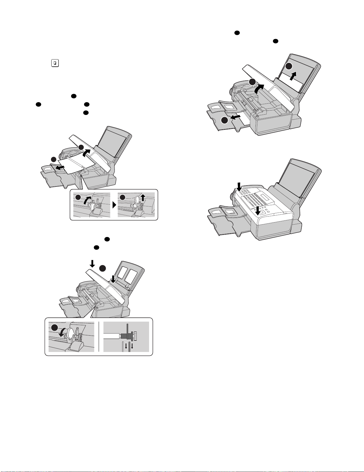
[7] Clearing paper jams
2
1
2
UX-B800A
2. Clearing jammed printing paper
1. Clearing a jammed document
If the original document doesn't feed properly during transmission or
copying, or [DOCUMENT JAMMED] appears in the display, first try
pressing . If the document doesn't feed out, remove it as
explained below.
Important: Do not try to remove a jammed document without releasing it as explained below. This may damage the feeder mechanism.
1) Open the cover ( ). Rotate the lever so that points straight up
COPY/HELP
1
2 3
( ), and pull it up ( ). Pull the roller out to the right, and
remove the document ( ).
4
4
1
2
3
1) Open the cover ( ). Pull the jammed paper forward or backward
out of the machine as appropriate ( ), taking care not to tear it.
2) Close the cover, pressing down firmly on both front corners.
1
2
2) Replace the white roller, inserting the left end first. Push the lever
down and rotate it back down ( ). Close the cover, pressing
firmly on both front corners ( ).
1
2
2
1
1 – 12
Page 14
UX-B800A
FUNCTION
[8] Quick reference guide
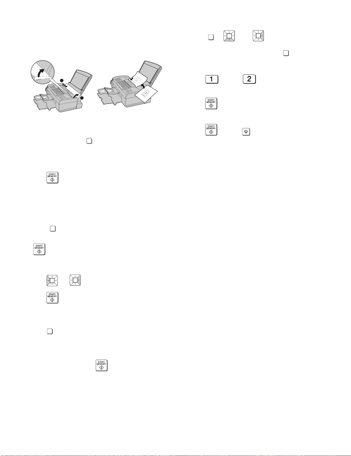
7. Storing Destinations
1. Fax / Scan to E-mail Transmission
Place your document (up to 20 pages) face down in the document
feeder.
2
1
2. Sending a Fax by Normal Dialing
1. Lift the handset or press .
2. Dial the fax number.
3. Wait for the reception tone (if a person answers, ask them to press
their Start key).
4. Press .
SPEAKER
3. Using a Rapid Key (fax/e-mail)
Press the Rapid Key for the destination.
1. Press , , then .
2. Press an unused Rapid Key, or press and enter an
SPEED DIAL
unused 2-digit Speed Dial number (01 to 63). (For an e-mail destination, you can also press the A, B or C key and go to Step 4.)
3. Press for fax or for e-mail.
4. Enter the fax number or the e-mail address.
5. Press .
6. Enter a name with the letter keys.
7. Press and then .
STOP
4. Using a Speed Dial number (fax/e-mail)
1. Press .
2. Enter the appropriate 2-digit Speed Dial number and press
SPEED DIAL
.
5. Searching for a destination (fax/e-mail)
1. Press or until the desired destination appears.
2. Press .
6. Receiving Faxes
RESOLUTION/
RECEPTION MODE
Press until the desired reception mode appears in the dis-
play.
AUTO mode: The machine automatically answers and receives faxes.
MANUAL mode: Answer all calls (even faxes) by picking up the hand-
set. To begin fax reception, press .
TEL/FAX mode: The machine automatically answers and receives
faxes. Voice calls are signalled by a special ringing sound.
1 – 13
Page 15

(step 1) Select "OPTION SETTING".
KEY : FUNCTION , , ,
DISPLAY: OPTION SETTING PRESS KEY
(step 2) Select "DIAL MODE".
KEY: , , , ,
DISPLAY: DIAL MODE
1: TONE, 2: PULSE
(step 3) Select, using "1" or "2".
KEY:
DISPLAY: TONE
KEY:
DISPLAY: PULSE
(step 4) End, using the "STOP" key.
(Press the STOP key three times.)
KEY:
1
2
STOP
1
Press or to select
HIGH,MIDDLE,LOW
,or
OFF
.
(Make sure has not been
pressed, the handset is not lifted,
and a document is not loaded in the
feeder.)
•
The ringer will ring once at the
selected level.
2
If you selected "
OFF OK ?
"toturn
off the ringer, press .
SPEAKER
START/
MEMORY
UX-B800A
CHAPTER 2. ADJUSTMENTS
[1] Adjustments
1. General description
Since the following adjustments and settings are provided for this
model, make adjustments and/or setup as necessary.
2. Adjustments of output voltage (FACTORY ONLY)
1. Install the power supply unit in the machine.
2. Set the recording paper and document.
3. When the document is loaded, power is supplied to the output
lines. Confirm that outputs are within the limits below.
2.1. Output voltage settings
1
15
CNLIU CNSP
CNPRT1 CNPRT2
CNCRMT
CNPW
CNLAN
CNENC CNFDMT
1
8
CNPN
CNSCANMT
CNCIS
CONTROL PWB
UX-B800A
4. Settings
Service Manual
4.1. Dial mode selector
DIAL mode (Soft Switch No. SW-9 Data No. 8)
Use this to set the fax machine to the type of telephone line you are
on.
• The factory setting is “TONE”.
18
CNPW
POWER SUPPLY PWB
Output Voltage limits
+5V 4.75 - 5.25V
+30V 27.0 - 33.0V
Pin No. CNPW
1 +30V
2 +30V
3MG
4MG
5DG
6DG
7+5V
8+5V
3. IC protectors replacement
ICPs (IC Protectors) are installed to protect the CIS and Ope amp. circuit. ICPs protect various ICs and electronic circuits from an overcurrent condition.
The location of ICPs are shown below:
CNPN
CNSCANMT
IC600
CNCIS
FU900
CNLAN
CNENC CNFDMT
CNPW
CONTROL PWB
(TOP VIEW)
1) FU900 (KAB5002) is installed in order to protect overcurrent +24V
supply. If FU900 is open, replace it with a new one.
LIU PWB
CNLIU
115
CNLIU CNSP
CNPRT1 CNPRT2
CNCRMT
5. Volume adjustments
5.1. Speaker volume
1
2
•
SPEAKER
Press .
Press or to select
HIGH,MIDDLE
SPEAKER
Press again to turn off the
speaker.
5.2. Ringer volume
2 – 1
,or
LOW
.
Page 16

UX-B800A
SOFT SWITCH MODE
SW123=00100100
Switch No.
12345678:DataNo.
SW =
SW1 =
[1] key
SW12 =
[2] key
SW123=00100100
[3] key
Cursor position
SW124=00000000
[START/MEMORY] key
SW125=00000000
SW123=00100100
[START/MEMORY] key
SW123=00100100
SW123=00100100
[>] or [#] key
SW124=00000000
With the cursor on data 8
[>] or [#] key
SW124=00000000
[>] or [#] key
SW124=00000000
SW124=00000000
[<] or [ ] key
SW123=00100100
With the cursor on data 1
[<] or [ ] key
SW123=00100100
[<] or [ ] key
SW124=00000000
[UP] or [4] key
SW123=00100100
SW125=00000000
[UP] or [4] key
SW124=00000000
[DOWN] or [6] key
SW125=00000000
SW123=00100100
[DOWN] or [6] key
[2] Diagnostics and service soft switch
1. Entering the diagnostic mode 2. Diagnostic items description
2.1. SOFT SWITCH MODE
FUNCTION
Press
display will appear
ROM:TF64
Then press the
Select the desired item with the
with the rapid key.
Enter the mode with the
•
specifications)
(Diag
FUNCTION
9 8
alternately.
: ROM version
START/MEMORY
START/MEMORY
9 8
7
7
key.
and the key or select
UP DOWN
key
key.
ROM:
TF64
, and
the
following
In this mode, the soft switches are set and the soft switch list is printed.
2.1.1 Operation
Soft switch mode screen
UP
START/MEMORY
START/MEMORY
START/MEMORY
START/MEMORY
START/MEMORY
START/MEMORY
START/MEMORY
START/MEMORY
START/MEMORY
START/MEMORY
START/MEMORY
START/MEMORY
START/MEMORY
START/MEMORY
START/MEMORY
START/MEMORY
START/MEMORY
START/MEMORY
DOWN
COUNTRY NAMEDIAG MODE
START/MEMORY
SOFT SWITCH MODE
ROM & RAM CHECK
AGING MODE
PANEL CHECK MODE
CHECK PATTERN MODE
SIGNAL SEND MODE
MEMORY CLEAR
SHADING MODE
AUTO FEEDER MODE
FLASH MEMORY CHECK
MEMORY SET MODE
CIS ADJUSTING MODE
SHARP CHART AGING
ASF AGING
IJP LIST MODE
LIFE MODE
LIFE CLEAR MODE
SECURE PASS LIST
2.1.2 Switch number selection and data setting
1. Enter three digits of a soft switch number to set the switch number.
Of a switch number of unexacting soft switch is entered, key error
buzzer sounds to reject the input.
2. Press [START/MEMORY] key moves the cursor to the data number
1 of the former soft switch. If the switch number is the final, pressing [START/MEMORY] key will exit the soft switch mode.
3. Data number selection
a) Pressing [>] or [#] key moves the cursor to the right. If the cursor
is on data number 8, pressing [>] or [#] key shifts the cursor to data
number 1 of the next switch number. If the switch number is the
final, pressing [>] or [#] key will exit the soft switch mode.
b) Pressing [<] or [ ] key moves the cursor to the left. If the cursor
is on data number 1, pressing [<] or [ ] key shifts the cursor to
data number 8 of the former switch number. If the switch number is
001, pressing [<] or [ ] key do not move the cursor.
c) Pressing [UP] or [4] key moves the cursor to the data number 1
of the next soft switch. If the switch number is 001, pressing [UP] or
[4] key shifts the cursor to data number 1.
d) Pressing [DOWN] or [6] key moves the cursor to the data number 1 of the former soft switch. If the switch number is the final,
pressing [down] or [6] key will exit the soft switch mode.
2 – 2
Page 17

e) Pressing [8] key moves the cursor to the data number 1 of the
To finish this mode, press [STOP] key
04:PANEL KEY TEST
1
[1] key
[2]Key
2
SPEAKER
Go to a) or b).
..... (other key)
[SPEAKER] key
Start by pressing the
[START/MEMORY] key
PRINTING
DIAG MODE
05:CHECK PATTERN
10th former soft switch.
SW123=00100100
SW113=00000000
[8] key
SW103=00000000
[8] key
f) Pressing [2] key moves the cursor to the data number 1 of the
10th next soft switch.
SW123=00100100
SW133=00000000
[2] key
SW143=00000000
[2] key
2.1.3 Data setting
Press the [1] key, and the data to the position of the cursor will be
changed to 1.
Press the [0] key, and the data to the position of the cursor will be
changed to 0.
2.1.4 Outputting method of soft switch list
In the soft switch mode, press [COPY/HELP] key, and the soft switch
list will be printed.
2.1.5 Storage of data
In the following cases, the data if the soft switches set will be stored.
• It is shifted to set the next soft switch by pressing [START/MEMORY] key.
• If is shifted to set the former soft switch with the [<] or [UP] or [4]
key.
• It is shifted to set the next soft switch with the [>] or [DOWN] or [6]
key.
• If is shifted to set the 10th former soft switch with the [8] key.
• It is shifted to set the 10th next soft switch with the [2] key.
2.2. ROM & RAM check
To check the sum value of Firmware or RAM.
No. Device Alarm Buzzer Remarks
1
2 SDRAM 3 times <Short
ROM
(PROGRAM FLASH)
Main
1 time <Short
sound>
sounds>
UX-B800A
2.4. PANEL CHECK MODE
This is used to check whether each key is normally operated or not.
After the test, the test result will be printed.
2.4.1 Flow
Press any key except [STOP] key. At this time, the name of each key
will be displayed every push of the key.
a) When all keys can be inputted, the following message will be displayed.
ALL KEY OK !!
Then the screen will be all displayed in black (refer to (2))and the test
result will be printed.
b) If any key skipped, the following message will be displayed.
KEY ERROR !!
A key name that is not pressed yet is displayed so that this test can be
continued.
At that time, pressing the [STOP] key will exit this mode. And the result
will be printed.
2.4.2 Black screen
2.2.1 Display
DIAG MODE
02:ROM & RAM CHECK
2.2.2 Result printing
After checking, the results print starts.
2.3. AGING MODE
A total of 10 sheets of check patterns are printed at 1-hour intervals.
This mode is exited when executed to the end (after 9 hours) or by
pressing the [STOP] key.
DIAG MODE
03:AGING MODE
WAITING
Start checking by pressing
[START/MEMORY] key
Start by pressing the
[START/MEMORY] key
SDRAM : OK
PRINTING
PRINTING
03:AGING MODE
Display during the aging
mode interval
2.5. CHECK PATTERN MODE
Printing the pattern.
2 – 3
Page 18

UX-B800A
AUTO FEEDER
[START/MEMORY] key
without document
DIAG MODE
09:AUTO FEEDER MODE
Only the sensor that is activated is displayed
DIAG MODE
A4 (A4 )
DIAG MODE
A4 (A4 ORG)
DIAG MODE
()
Set document
[START/MEMORY] key
without document
WAIT A MOMENT
DIAG MODE
10:FLASH MEM. CHECK
FLASH CHECK
PRESS START OR STOP
[START/MEMORY] key
[STOP] key
Next daig mode
[START/MEMORY] key
PRINTING
Start
DIAG MODE
11:MEMORY SET MODE
MEMORY SET MODE
xxxxxxxx= [ ]
[START/MEMORY] key
Address entry screen
Entry of memory address (8 digits)
MEMORY SET MODE
1234ABCD=4C [L]
Hex
number
Character
code
• Change of memory contents: 2-digit entry in hex number
• Move down the address of the referenced memory by one: [<] or [UP] key
• Move up the address of the referenced memory by one: [>] or [DOWN] key
• Dump list print: [COPY/HELP] key
• Back to the address entry screen: [STOP] key
The contents of the memory are displayed
in hex number and character code.
2.6. SIGNAL SEND MODE
The specified signals are transmitted in the following sequence to
check the modem.
1. Press the [START/MEMORY] key, and no signals with the loop
state starts.
[1] No signals (making the loop)
[2] 14400BPS (V.17)
[3] 12000BPS (V.17)
[4] 9600BPS (V.17)
[5] 7200BPS (V.17)
[6] 9600BPS (V.29)
[7] 7200BPS (V.29)
[8] 4800BPS (V.27ter)
[9] 2400BPS (V.27ter)
[10] 300BPS (FLAG)
[11] 2100Hz (CED)
[12] 1100Hz (CNG)
DIAG MODE
06:SIGNAL SEND MODE
[START/MEMORY] Key
SIG SEND MODE
V.17 7200bps V.17 9600bps
[START/MEMORY] Key
V.29 9600bps V.29 7200bps
2100 Hz (CED TONE) FLAG (300bps)
[ENTER]Key
1100 Hz (CNG)
[START/MEMORY] Key
[START/MEMORY] Key
[START/MEMORY] Key
[ENTER]Key
CML ON
[START/MEMORY] Key
V.17 14400bps
[START/MEMORY] Key
[START/MEMORY] Key
V.17 12000bps
[START/MEMORY] Key
V.27ter 4800bps
[START/MEMORY] Key
[START/MEMORY] Key
V.27ter 2400bps
2.9. AUTO FEEDER MODE
Inserting and discharging the document can check the auto feeder.
1. The information of document sensor (A4 sensor) and ORG sensor
is displayed when the documents are inserted to the Auto Feeder.
Press the [START/MEMORY] key, and feeding documents is
started.
2. Press [STOP] key to exit the mode.
2.10. FLASH MEMORY CHECK
Read/write of the flash memory is checked.
The result is printed after completion of check.
Be sure to clear the memory after execution.
2. Pressing the [START/MEMORY] key during transmitting CNG signal, or pressing the [STOP] key will stop the output of signal and
exit the mode.
2.7. MEMORY CLEAR
Clear the back-up memory including the soft switches, registration
data. After executing this mode, the memory clear report is printed.
Note: The following data is not cleared. Values for Printer life including
the adjusted value of printing void.
DIAG MODE
07:MEMORY CLEAR
Start by pressing the
[START/MEMORY] key
2.8. SHADING MODE
Shading waveforms are stored.
Set a shading sheet and press the [START/MEMORY] key to start
shading.
DIAG MODE
08:SHADING MODE
Start by pressing the
[START/MEMORY] key
MEMORY CLEARD
PRINTING
TOTAL SHADING
2.11. MEMORY SET MODE
It is possible to read or write the memory contents.
When 8 digits of physical address are entered, the data of that address
is displayed.
When 2 digits of data are entered after entering 8 digits of address and
a key is pressed, the contents can be rewritten.
Rewriting is enabled only in the range of addresses 00000000 to
007FFFFF.
If the memory is rewritten, the machine may malfunction.
Press the [STOP] key on the address entry screen to exit the mode.
2 – 4
Page 19

2.12. CIS ADJUSTING MODE
Start by pressing the
[START/MEMORY] key
MACH.COUNT=0123456789
DIAG MODE
16:LIFE MODE
STAND-BY state
Press
FUNKTION
Start by pressing the
[START/MEMORY] key
DIAG MODE
17:LIFE CLEAR MODE
Start by pressing the
[START/MEMORY] key
DIAG MODE
18:SECURE PASS LIST
In this mode, the position of Scanner motor is moved from the home
position up to the specified value. And document reading lamp is
turned on.
DIAG MODE
12:CIS ADJUST
[START/MEMORY] key
CIS ADJUST MODE
The motor will move to the specified position and the reading lamp is lit on.
[START/MEMORY] key
Press the [STOP] key to exit the mode.
2.13. SHARP CHART AGING
SHARP CHART is printed continuously.
UX-B800A
2.16. LIFE MODE
MACHINE PAGE COUNT is displayed.
Press the [STOP] key to exit the mode.
• LIFE MODE can also be checked by the following operation.
2.17. LIFE CLEAR MODE
MACHINE DOT COUNT and MACHINE PAGE COUNT are cleared.
DIAG MODE
13:SHARP CHART AGING
Start by pressing the
[START/MEMORY] key
SHARP CHART AGING
PRINTING P.1
Press the [STOP] key for interruption.
2.14. ASF AGING
The recording paper is fed continuously.
DIAG MODE
14:ASF AGING
Start by pressing the
[START/MEMORY] key
ASF AGING
Press the [STOP] key for interruption.
2.15. IJP LIST MODE
Maintenance data of the printer is output.
MACHINE DOT COUNT Machine total dot count
MACHINE PAGE COUNT Machine total page count
CARTRIDGE DOT COUNT Cartridge-by-cartridge dot count
IDLE MAINTENANCE COUNT Maintenance information
INSTALL MAINTENANCE
COUNT
BEGIN OF JOB MAINTENANCE
COUNT
THRESHOLD MAINTENANCE
COUNT
POJ MAINTENANCE COUNT Maintenance information
SWATH START TEMPERA-
TURE
FUSE MEMORY VALUE Cartridge information
VPH ON TIME Cartridge information
CARTRIDGE CHANGE COUNT Cartridge replacement count
JAM COUNT Jam count
NOZZLE CLEAN COUNT Nozzle cleaning count
CALIBRATION ENVIRONMENT
TEMPERATURE
CALIBRATION PRINT HEAD
TEMPERATURE
TEMPERATURE MODE Temperature control information
Maintenance information
Maintenance information
Maintenance information
Temperature control information
Environmental temperature information
Cartridge temperature information
2.18. SECURE PASS LIST
Print the SECURE PASS LIST.
DIAG MODE
15:IJP LIST MODE
Start by pressing the
[START/MEMORY] key
PRINTING
2 – 5
Page 20

UX-B800A
3. How to make soft switch setting
To enter the soft switch mode, press the following key entries in sequence.
Press
FUNCTION
9 8 START/MEMORYSTART/MEMORY
DATA No. 1 2 3 4 5 6 7 8
SW001 = 0 0 0 0 0 0 0 0
SW001 = 1 0 0 0 0 0 0 0
SW001 = 1 0 0 0 0 0 0 0
SW001 = 1 0 0 0 0 0 0 0
SW001 = 1 0 0 0 0 0 0 0
SW002 = 0 0 0 0 0 0 0 0
SW300 = 0 0 0 0 0 0 0 0
7
Press 1 or key.
Press or key.
Press or key.
Bit1 - 8 are set.
Press key during setting.
Soft SW002 - SW300 are set.
To finish the settings halfway between
SW001 and SW300, press the STOP
key. In this case, the setting being done
to the SW No. on display will be nullified
while settings done to the preceding
SW No. remain in effect.
When the COPY/HELP key is pressed, the
contents of soft switches are printed.
0
<
>
START/MEMORY
0
1
0
The soft switch mode is terminated.
2 – 6
Page 21

4. Soft switch description
4.1. Soft switch
UX-B800A
SW
NO.
SW
1
SW
2
SW
3
SW
4
SW
5
SW
6
DATA
NO.
1Reserved 0
2Reserved 0
Receive mode FAX TEL TEL/
3
4
5Reserved 1
6Reserved 0
7Reserved 0
8Reserved 0
1Reserved 0
2 Forced 4800BPS reception Yes No 0
CED tone signal interval 75ms 500ms 750ms 1000ms
3
4
5Reserved 0
6Reserved 0
7Reserved 0
8Reserved 0
1 Length limitation of receive No limit Receive 1.5m 0
2 Footer print Yes No 0
3Reserved 0
4Reserved 0
5Reserved 0
6Reserved 0
7 CSI transmission Not transmitted Transmitted 0
8 Action when RTN is received No communication error Communication error 0
1Reserved 1
2 Dial pausing (sec/pause) 4sec 2sec 0
3 Pulse format of D.P. N+1 N 0
4 DIS receive acknowledgement dur-
ing G3 transmission
5 Non-modulation carrier for V29
transmission mode
6Reserved 0
7 Protocol monitor Yes No 0
8 Line monitor Yes No 0
1Reserved 0
2Reserved 0
3Reserved 0
4Reserved 0
5Reserved 0
6Reserved 0
7Reserved 0
8Reserved
1Reserved 0
2Reserved 0
3 Digital cable equalizer for Reception Yes No 0
4 Sender's information transmit No Yes 0
5Reserved 1
6Reserved 0
7Reserved 0
8Reserved 0
ITEM
No.30011
No.40101
No.30011
No.40101
Twice NSF: Once
Yes No 0
Switch setting and function
10
FAX
FAX
DIS: Twice
Initial
setting
0
0
0
0
0
0
Remarks
2 – 7
Page 22

UX-B800A
SW
NO.
SW
7
SW
8
DATA
NO.
1 H2 mode No Yes 0
2 Reserved 1
3 ECM mode No Yes 0 OPTION
4 ECM MMR mode No Yes 0
Signal transmission level 1
5
6
7
8
Recall interval (FAX) 0
1
2
3
4
Recall times (FAX) 0
5
6
7
8
ITEM
Switch setting and function
10
Binary input
No. = 8 4 2 1
5678(DataNo.)
EX1111
eg. -8dBm
Binary input
No. = 8 4 2 1
1234(DataNo.)
EX0101
eg. 5 minutes
Binary input
No. = 8 4 2 1
5678(DataNo.)
EX0010
eg. 3 times
Initial
setting
1
1
1
1
0
1
0
1
0
Remarks
Setting:
N = 1 to 9
Setting:
N = 1 to 9
1 Reserved 0
2 Reserved 0
3 Reserved 0
4 Sort copy function Yes No 0 PRINT SETUP
SW
9
5 Reserved 0
6 Reserved 0
7 Reserved 0
8 Dial mode Pulse Tone 0
1 Reserved 1
2 Reserved 0
3 CNG detection Yes No 1 OPTION
4 Number of CNG detection 3 pulses 2 pulses 0
SW
5 Signal detect time in TEL/FAX mode 3sec 1sec 0
10
6 Reserved 0
CNG detection time after ringing
7
8
1 Reserved 0
2 Reserved 1
3 Time display format 24hours 12hours-AM/PM 1
4 Date display format Month-Day-Year Day-Month-Year 0
SW
11
Pseudo ringing time at TEL/FAX
automatic switching mode
5
6
7 Reserved 0
8 CED detection time 500ms 1000ms 0
No. 7 0 0 1 1
No. 8 0 1 0 1
No. 5 0 0 1 1
No. 6 0 1 0 1
20sec 10sec 30sec No limit
0
0
15sec 30sec 60sec 120sec
0
0
OPTION
2 – 8
Page 23

UX-B800A
SW
NO.
SW
12
SW
13
SW
14
SW
15
SW
16
SW
17
DATA
NO.
1 MH fixed Yes No 0
2 Reserved 0
3 Reserved 0
4 Reserved 0
5 Reserved 0
6 Key tone OFF ON 0 OPTION
7 Reserved 0
8 Reserved 0
1 Reserved 0
2 Reserved 0
3 Reserved 0
4 Reserved 0
5 Reserved 0
6 Reserved 0
7 Reserved 0
8 Reserved 0
1 Reserved 0
2 Reserved 0
3 Reserved 0
4 Reserved 0
Modem speed No. 5 No.6 No. 7 No. 8
5
6
7
8
1 Reserved 0
2 Reserved 0
3 Reserved 0
4 Reserved 1
5 Reserved 1
6 Reserved 0
7 Reserved 0
8 Reserved 1
1 Digital cable equalizer for transmis-
sion
2 Reserved
3 Reserved 0
4 Flash send time Long time Short time 0 OPTION
Flash short time 90ms 100ms 110ms 125ms
5
6
Flash long time 250ms 230ms 270ms 280ms
7
8
1 Reserved 0
2 Reserved 1
3 Reserved 0
4 Reserved 0
5 Reserved 0
6 Reserved 1
7 Reserved 0
8 Reserved 0
ITEM
V.17 14400bps 1000
V.17 12000bps 1010
V.17 9600bps 1001
V.17 7200bps 1011
V.29 9600bps 0001
V.29 7200bps 0011
V.27ter 4800bps 0010
V.27ter 2400bps 0000
Yes N o 0
No. 50011
No. 60101
No. 70011
No. 80101
Switch setting and function
10
Initial
setting
1
0
0
0
0
0
0
0
0
Remarks
2 – 9
Page 24

UX-B800A
SW
NO.
SW
18
SW
19
SW
20
SW
21
SW
22
SW
23
DATA
NO.
1 Reserved 0
2 Reserved 0
3 Reserved 0
4 Reserved 0
5 Reserved 0
6 Reserved 0
7 Reserved 0
8 Reserved 0
1 Reserved 1
2 Reserved 0
3 Reserved 0
4 Reserved 0
5 Reserved 0
6 Reserved 1
7 Reserved 0
8 Reserved 0
1 Reserved 0
2 Reserved 1
3 Reserved 0
4 Reserved 1
5 Reserved 1
6 Reserved 0
7 Reserved 0
8 Reserved 0
Line density selection STAN-
1
2
Communication results printout Error
3
4
5
6 Caller ID function Yes No 0 OPTION
7 Activity report print Yes (When memory full) No (First data is cleared when
8 Day Light Saving (Summer time) No Yes 1
1 Activate Receive Fax to E-mail Yes No 0
2 Print setting of received fax for
Receive Fax to E-mail
3 Report setting for Receive Fax to E-
mail
4 Activate Secure Receive Yes No 0
5 Reserved 0
6 Reserved 0
7 Reserved 0
8 Reserved 0
1 Ink Save Mode Setting ON OFF 0 PRINT SETUP
2 Receive Reduce Setting 100% Auto 0 PRINT SETUP
Paper Size LET-
3
4
5 Half tone copy print swath direction Single direction printing Both direction printing 1 PRINT SETUP
6 Reserved 0
7 Reserved 0
8 Reserved 0
ITEM
No. 1 0 0 1 1
No. 2 0 1 0 1
No. 300011
No. 400101
No. 510000
Print at error Always Print 0
Print at error Always Print 1
No. 3 0 0 1 1
No. 4 0 1 0 1
Switch setting and function
10
FINE S-FINE STAN-
DARD
Only
TER
Error/
Memory
A4 LEGAL LET-
Send
only
memory full)
DARD
No Print Always
TER
Initial
setting
0
0
0
0
1
0OPTION
0
1
Remarks
OPTION
(Only for Stan-
dard/Fine)
OPTION
(Only for A4)
2 – 10
Page 25

UX-B800A
SW
NO.
SW
24
SW
25
SW
26
SW
27
SW
28
SW
29
SW
30
DATA
NO.
1 Reserved 0
2 Reserved 0
3 Reserved 0
4 Reserved 0
5 Reserved 0
6 Reserved 0
7 Reserved 0
8 Reserved 0
1 Reserved 0
2 Reserved 0
3 Reserved 0
4 Reserved 0
5 Reserved 1
6 Reserved 0
7 Reserved 0
8 Reserved 1
1 Reserved 0
2 Reserved 0
3 Reserved 0
4 Reserved 0
5 Reserved 0
6 Reserved 0
7 Reserved 0
8 Reserved 0
1 Reserved 0
2 Reserved 0
3 Reserved 0
4 Reserved 0
5 Reserved 0
6 Reserved 0
7 Reserved 0
8 Reserved 0
1 Reserved 0
2 Reserved 0
3 Reserved 0
4 Reserved 0
5 Reserved 1
6 Reserved 0
7 Reserved 0
8 Reserved 1
1 Reserved 0
2 Reserved 0
3 Reserved 0
4 Reserved 0
5 Reserved 0
6 Reserved 0
7 Reserved 0
8 Reserved 0
1 Reserved 0
2 Reserved 1
3 Reserved 0
4 Reserved 0
5 Reserved 0
6 Reserved 0
7 Reserved 0
8 Reserved 0
ITEM
Switch setting and function
10
Initial
setting
Remarks
2 – 11
Page 26

UX-B800A
SW
NO.
SW
31
SW
32
SW
33
SW
34
SW
35
SW
36
SW
37
DATA
NO.
1Reserved 0
2Reserved 0
3Reserved 0
4Reserved 0
5Reserved 0
6Reserved 0
7Reserved 0
8Reserved 0
1Reserved 0
2Reserved 0
3Reserved 0
4 Error criterion 10-20% 5-10% 0
EOL (End of Line) detection timer 13sec 25sec 5sec
5
6
7Reserved 0
8Reserved 0
1Reserved 0
2Reserved 0
3Reserved 0
4Reserved 0
5Reserved 0
6Reserved 0
7Reserved 0
8Reserved 0
1Reserved 0
2Reserved 0
3Reserved 0
4Reserved 0
5Reserved 0
6Reserved 0
7Reserved 0
8Reserved 0
1Reserved 0
2Reserved 0
3Reserved 0
4Reserved 0
5Reserved 0
6Reserved 0
7Reserved 0
8Reserved
1Reserved 0
2Reserved 0
3Reserved 0
4Reserved 0
5Reserved 0
6Reserved 0
7Reserved 0
8Reserved 0
1Reserved 0
2Reserved 0
3Reserved 0
4Reserved 0
5Reserved 0
6Reserved 0
7Reserved 0
8Reserved 0
ITEM
No. 5001
No. 6010
Switch setting and function
10
Initial
setting
0
0
0
Remarks
2 – 12
Page 27

UX-B800A
SW
NO.
SW
38
SW
39
SW
40
SW
41
SW
42
SW
43
DATA
NO.
1Reserved 0
2Reserved 0
3Reserved 0
4Reserved 0
5Reserved 0
6Reserved 0
7Reserved 0
8Reserved 0
1Reserved 0
2Reserved 1
3Reserved 1
4Reserved 0
5Reserved 0
6Reserved 0
7 Make/Break ratio in D.P. 40/60 33/67 0
8 Pre pause time in D.P. 320ms 50ms 0
Inter digit pause time No. 1 No. 2 No. 3
1
2
3
4
Change to PB from PB by key
5Reserved 0
6Reserved 0
7Reserved 0
8Reserved 0
DTMF detect time 50ms 80ms 100ms 120ms
1
2
3 Protection of remote reception
(5 ) detect
Remote operation code figure by
external TEL(0-9)
4
5
6
7
8Reserved 0
1Reserved 0
2Reserved 1
3Reserved
4Reserved 0
5Reserved 0
6Reserved 0
7Reserved 0
8Reserved 0
1Reserved 0
2Reserved 0
3Reserved 0
4Reserved 0
5Reserved 0
6Reserved 0
7Reserved 0
8Reserved 0
ITEM
800ms 0 0 0
840ms 0 0 1
880ms 0 1 0
900ms 0 1 1
1000ms 1 0 0
Not used 1 0 1
Not used 1 1 0
Not used 1 1 1
Yes No 1
No. 10011
No. 20101
Yes No 0
Switch setting and function
10
Binary input
No. = 8 4 2 1
4567(DataNo.)
EX0101
eg. Remote operation code is set "5 "
Initial
setting
0
0
0
0
0
0
1
0
1
1
Remarks
OPTION
2 – 13
Page 28

UX-B800A
SW
NO.
SW
44
SW
45
SW
46
SW
47
SW
48
SW
49
SW
50
DATA
NO.
1 Reserved 1
2 Reserved 0
3 Reserved 0
4 Reserved 0
5 Reserved 0
6 Reserved 0
7 Reserved 0
8 Reserved 0
1 Reserved 0
2 Reserved 0
3 Reserved 0
4 Reserved 0
5 Reserved 0
6 Reserved 0
7 Reserved 0
8 Reserved 0
1 Reserved 0
2 Reserved 0
3 Reserved 0
4 Reserved 0
5 Reserved 0
6 Reserved 0
7 Reserved 0
8 Reserved 0
1 Reserved 0
2 Reserved 0
3 Reserved 0
4 Reserved 0
5 Reserved 0
6 Reserved 0
7 Reserved 0
8 Reserved 0
1 Reserved 0
2 Reserved 0
3 Reserved 1
4 Reserved 0
5 Reserved 0
6 Reserved 1
7 Reserved 1
8 Reserved 0
1 Reserved 0
2 Reserved 0
3 Reserved 0
4 Reserved 0
5 Reserved 0
6 Reserved 0
7 Reserved 0
8 Reserved 0
1 Reserved 0
2 Reserved 0
3 Reserved 0
4 Reserved 0
5 Reserved 0
6 Reserved 0
7 Reserved 0
8 Reserved 0
ITEM
Switch setting and function
10
Initial
setting
Remarks
2 – 14
Page 29

UX-B800A
SW
NO.
SW
51
SW
52
SW
53
SW
54
SW
55
SW
56
SW
57
DATA
NO.
1 Reserved 0
2 Reserved 0
3 Reserved 0
4 Reserved 0
5 Reserved 0
6 Busy tone detect when TEL/FAX
mode
7 Dial tone detect when TEL/FAX
mode
8 Reserved 0
1 Reserved 0
2 Reserved 0
3 Reserved 0
4 Reserved 0
5 Reserved 1
6 Reserved 0
7 Reserved 0
8 Reserved 0
1 Reserved 1
2 Reserved 0
3 Reserved 1
4 Reserved 0
5 Reserved 0
6 Reserved 0
7 Reserved 0
8 Reserved 1
1 Reserved 0
2 Reserved 0
3 Reserved 0
4 Reserved 1
5 Reserved 0
6 Reserved 1
7 Reserved 0
8 Reserved 0
1 Reserved 0
2 Reserved 1
3 Reserved 0
4 Reserved 1
5 Reserved 0
6 Reserved 1
7 Reserved 0
8 Reserved
1 Reserved 0
2 Reserved 1
3 Reserved 0
4 Reserved 0
5 Reserved 1
6 Reserved 0
7 Reserved 0
8 Reserved 0
1 Reserved 0
2 Reserved 0
3 Reserved 0
4 Reserved 0
5 Reserved 0
6 Reserved 0
7 Reserved 0
8 Reserved 0
ITEM
No Yes 0
No Yes 0
Switch setting and function
10
Initial
setting
1
Remarks
2 – 15
Page 30

UX-B800A
SW
NO.
SW
58
SW
59
SW
60
SW
61
SW
62
SW
63
SW
64
DATA
NO.
1Reserved 0
2Reserved 0
3Reserved 0
4Reserved 0
5Reserved 0
6Reserved 0
7Reserved 0
8Reserved 0
1Reserved 0
2Reserved 0
3Reserved 0
4Reserved 0
5Reserved 0
6Reserved 0
7Reserved 0
8Reserved 0
1Reserved 0
2Reserved 0
3Reserved 1
4Reserved 0
5Reserved 0
6Reserved 1
7Reserved 0
8Reserved 0
1Reserved 1
2Reserved 1
Ringer Volume OFF LOW MIDDLE HIGH
3
4
Speaker Volume LOW LOW MIDDLE HIGH
5
6
7Reserved 1
8Reserved 0
1Reserved 0
2Reserved 1
3Reserved 1
4Reserved 0
5Reserved 1
6Reserved
7Reserved 0
8Reserved 0
1Reserved 0
2Reserved 1
3Reserved 0
4Reserved 0
5Reserved 1
6Reserved 0
7Reserved 0
8Reserved 0
1Reserved 0
2Reserved 1
3Reserved 0
4Reserved 1
5Reserved 0
6Reserved 0
7Reserved 1
8Reserved 0
ITEM
No. 30011
No. 40101
No. 50011
No. 60101
Switch setting and function
10
Initial
setting
0
1
0
1
1
Remarks
2 – 16
Page 31

UX-B800A
SW
NO.
SW
65
SW
66
SW
67
SW
68
SW
69
SW
70
SW
71
DATA
NO.
1 Reserved 0
2 Reserved 1
3 Reserved 1
4 Reserved 0
5 Reserved 0
6 Reserved 1
7 Reserved 0
8 Reserved 0
1 Reserved 0
2 Reserved 1
3 Reserved 1
4 Reserved 0
5 Reserved 1
6 Reserved 0
7 Reserved 0
8 Reserved 0
1 Reserved 0
2 Reserved 0
3 Reserved 0
4 Reserved 0
5 Reserved 0
6 Reserved 0
7 Reserved 0
8 Reserved 0
1 Reserved 0
2 Reserved 0
3 Reserved 0
4 Reserved 0
5 Reserved 0
6 Reserved 0
7 Reserved 0
8 Reserved 0
1 Reserved 0
2 Reserved 0
3 Reserved 0
4 Reserved 0
5 Reserved 0
6 Reserved 0
7 Reserved 0
8 Reserved 0
1 Reserved 0
2 Reserved 0
3 Reserved 1
4 Reserved 0
5 Reserved 1
6 Reserved 0
7 Reserved 0
8 Reserved 0
1 Reserved 1
2 Reserved 0
3 Reserved 1
4 Reserved 1
5 Reserved 0
6 Reserved 0
7 Reserved 0
8 Reserved 0
ITEM
Switch setting and function
10
Initial
setting
Remarks
2 – 17
Page 32

UX-B800A
SW
NO.
SW
72
SW
73
SW
74
SW
75
SW
76
SW
77
SW
78
DATA
NO.
1 Reserved 0
2 Reserved 0
3 Reserved 1
4 Reserved 0
5 Reserved 1
6 Reserved 1
7 Reserved 1
8 Reserved 0
1 Reserved 0
2 Reserved 0
3 Reserved 0
4 Reserved 1
5 Reserved 0
6 Reserved 0
7 Reserved 0
8 Reserved 0
1 Reserved 0
2 Reserved 0
3 Reserved 0
4 Reserved 0
5 Reserved 0
6 Reserved 1
7 Reserved 0
8 Reserved 0
1 Reserved 1
2 Reserved 1
3 Reserved 0
4 Reserved 0
5 Reserved 0
6 Reserved 1
7 Reserved 0
8 Reserved 0
1 Reserved 0
2 Reserved 0
3 Reserved 0
4 Reserved 0
5 Reserved 0
6 Reserved 1
7 Reserved 0
8 Reserved 0
1 Reserved 0
2 Reserved 0
3 Reserved 1
4 Reserved 1
5 Reserved 0
6 Reserved 0
7 Reserved 0
8 Reserved 0
1 Reserved 1
2 Reserved 0
3 Reserved 0
4 Reserved 1
5 Reserved 0
6 Reserved 1
7 Reserved 0
8 Reserved 0
ITEM
Switch setting and function
10
Initial
setting
Remarks
2 – 18
Page 33

UX-B800A
SW
NO.
SW
79
SW
80
SW
81
SW
82
SW
83
SW
84
SW
85
DATA
NO.
1 Reserved 0
2 Reserved 0
3 Reserved 0
4 Reserved 1
5 Reserved 0
6 Reserved 0
7 Reserved 1
8 Reserved 0
1 Reserved 0
2 Reserved 0
3 Reserved 0
4 Reserved 0
5 Reserved 0
6 Reserved 0
7 Reserved 0
8 Reserved 0
1 Reserved 1
2 Reserved 1
3 Reserved 1
4 Reserved 0
5 Reserved 0
6 Reserved 0
7 Reserved 0
8 Reserved 0
1 Reserved 0
2 Reserved 0
3 Reserved 1
4 Reserved 0
5 Reserved 0
6 Reserved 0
7 Reserved 1
8 Reserved 1
1 Reserved 0
2 Reserved 0
3 Reserved 0
4 Reserved 0
5 Reserved 0
6 Reserved 0
7 Reserved 0
8 Reserved 0
1 Reserved 0
2 Reserved 0
3 Reserved 0
4 Reserved 0
5 Reserved 0
6 Reserved 0
7 Reserved 0
8 Reserved 0
1 Reserved 0
2 Reserved 0
3 Reserved 0
4 Reserved 0
5 Reserved 0
6 Reserved 0
7 Reserved 0
8 Reserved 0
ITEM
Switch setting and function
10
Initial
setting
Remarks
2 – 19
Page 34

UX-B800A
SW
NO.
SW
86
SW
87
SW
88
SW
89
SW
90
SW
91
SW
92
DATA
NO.
1 Reserved 0
2 Reserved 0
3 Reserved 0
4 Reserved 1
5 Reserved 0
6 Reserved 0
7 Reserved 1
8 Reserved 1
1 Reserved 0
2 Reserved 0
3 Reserved 0
4 Reserved 0
5 Reserved 0
6 Reserved 0
7 Reserved 0
8 Reserved 0
1 Reserved 0
2 Reserved 0
3 Reserved 1
4 Reserved 0
5 Reserved 1
6 Reserved 0
7 Reserved 1
8 Reserved 0
1 Reserved 0
2 Reserved 1
3 Reserved 1
4 Reserved 0
5 Reserved 0
6 Reserved 0
7 Reserved 0
8 Reserved 0
1 Reserved 0
2 Reserved 0
3 Reserved 0
4 Reserved 0
5 Reserved 0
6 Reserved 0
7 Reserved 0
8 Reserved 0
1 Reserved 0
2 Reserved 0
3 Reserved 0
4 Reserved 0
5 Reserved 0
6 Reserved 0
7 Reserved 0
8 Reserved 0
1 Reserved 0
2 Reserved 0
3 Reserved 0
4 Reserved 0
5 Reserved 0
6 Reserved 0
7 Reserved 0
8 Reserved 0
ITEM
Switch setting and function
10
Initial
setting
Remarks
2 – 20
Page 35

UX-B800A
SW
NO.
SW
93
SW
94
SW
95
SW
96
SW
97
SW
98
SW
99
DATA
NO.
1 Reserved 0
2 Reserved 0
3 Reserved 0
4 Reserved 0
5 Reserved 0
6 Reserved 0
7 Reserved 0
8 Reserved 0
1 Reserved 0
2 Reserved 1
3 Reserved 0
4 Reserved 0
5 Reserved 1
6 Reserved 0
7 Reserved 0
8 Reserved 0
1 Reserved 0
2 Reserved 1
3 Reserved 0
4 Reserved 0
5 Reserved 1
6 Reserved 1
7 Reserved 0
8 Reserved 0
1 Reserved 0
2 Reserved 0
3 Reserved 0
4 Reserved 0
5 Reserved 0
6 Reserved 1
7 Reserved 0
8 Reserved 0
1 Reserved 0
2 Reserved 0
3 Reserved 0
4 Reserved 0
5 Reserved 0
6 Reserved 0
7 Reserved 0
8 Reserved 0
1 Reserved 0
2 Reserved 0
3 Reserved 0
4 Reserved 1
5 Reserved 1
6 Reserved 0
7 Reserved 0
8 Reserved 1
1 Reserved 0
2 Reserved 1
3 Reserved 0
4 Reserved 0
5 Reserved 0
6 Reserved 0
7 Reserved 0
8 Reserved 0
ITEM
Switch setting and function
10
Initial
setting
Remarks
2 – 21
Page 36

UX-B800A
SW
NO.
SW
100
SW
101
SW
102
SW
103
SW
104
SW
105
SW
106
DATA
NO.
1 Reserved 1
2 Reserved 1
3 Reserved 1
4 Reserved 1
5 Reserved 1
6 Reserved 0
7 Reserved 0
8 Reserved 0
1 Reserved 0
2 Reserved 0
3 Reserved 0
4 Reserved 0
5 Reserved 0
6 Reserved 0
7 Reserved 0
8 Reserved 0
1 Reserved 0
2 Reserved 0
3 Reserved 0
4 Reserved 0
5 Reserved 0
6 Reserved 0
7 Reserved 0
8 Reserved 0
1 Reserved 0
2 Reserved 0
3 Reserved 0
4 Reserved 0
5 Reserved 0
6 Reserved 0
7 Reserved 0
8 Reserved 0
1 Reserved 0
2 Reserved 0
3 Reserved 0
4 Reserved 0
5 Reserved 0
6 Reserved 0
7 Reserved 0
8 Reserved 0
1 Reserved 0
2 Reserved 0
3 Reserved 0
4 Reserved 0
5 Reserved 0
6 Reserved 0
7 Reserved 0
8 Reserved 0
1 Reserved 0
2 Reserved 0
3 Reserved 0
4 Reserved 0
5 Reserved 0
6 Reserved 0
7 Reserved 0
8 Reserved 0
ITEM
Switch setting and function
10
Initial
setting
Remarks
2 – 22
Page 37

UX-B800A
SW
NO.
SW
107
SW
108
SW
109
SW
110
DATA
NO.
1 Reserved 0
2 Reserved 0
3 Reserved 0
4 Reserved 0
5 Reserved 0
6 Reserved 0
7 Reserved 0
8 Reserved 0
1 Reserved 1
2 Reserved 0
3 Reserved 0
4 Reserved 1
5 Reserved 0
6 Reserved 0
7 Reserved 0
8 Reserved 0
1 Reserved 0
2 Reserved 1
3 Reserved 1
4 Reserved 0
5 Reserved 0
6 Reserved 0
7 Reserved 0
8 Reserved 0
Connect configuration for LAN controller
1
2
3
4 Reserved 0
5 Reserved 0
6 Reserved 0
7 Reserved 0
8 Reserved 0
Detect time of LAN link ON
ITEM
Default (Auto) 0 0 0
Full duplex 100M 0 0 1
Full duplex 10M 0 1 0
Auto 011
Half duplex 100M 1 0 0
Half duplex 10M 1 0 1
Switch setting and function
10
No. 1 No. 2 No. 3
Initial
setting
1
0
1
Remarks
1 - 15 seconds
SW
111
1
2
3
4
Detect time of LAN link OFF
5
6
7
8
Binary input
No. = 8 4 2 1
1234(DataNo.)
EX0100=4seconds
Note:"0000"=1UGEQPF
Binary input
No. = 8 4 2 1
5678(DataNo.)
EX0100=4seconds
Note:"0000"=1UGEQPF
2 – 23
0
0
0
0
1 - 15 seconds
0
0
0
0
Page 38

UX-B800A
SW
NO.
SW
112
SW
113
SW
114
DATA
NO.
1 Default file format for network scan PDF TIFF 0 Network setting
Default resolution for network scan Stan-
2
3
4 Reserved 0
5 Reserved 0
6 Reserved 0
7 Reserved 0
8 SMTP authentication type All of GEMINI’s support type Confirm server support type 0 Only when
1 Reserved 0
2 Reserved 0
3 Reserved 0
4 Reserved 0
5 Reserved 0
6 Reserved 0
7 Reserved 0
8 Reserved 0
DTMF output level (High)
1
2
3
4
5
6 Reserved 0
7 Reserved 0
8 Reserved 0
DTMF output level (Low)
ITEM
No. 2 0 0 1
No. 3 0 1 0
Switch setting and function
10
Fine S-Fine
dard
Binary input
No.= 168421
1 2 3 4 5 (Data No.)
EX1 0011
eg. Signal transmission level is set to -10dBm
Initial
setting
0
1
1
0
0
1
1
Remarks
Network setting
SMTP-auth
supported
Binary input
1
2
SW
3
115
4
5
6 Reserved 0
7 Reserved 0
8 Reserved 0
Dial tone detection frequency No. 1 No. 2 No. 3
1
2
SW
3
116
Busy tone detection frequency No. 1 No. 2
4
5
6 Reserved 0
7 Reserved 0
8 Reserved 1
No.= 168421
1 2 3 4 5 (Data No.)
EX1 0110
eg. Signal transmission level is set to -10dBm
280 - 520Hz 0 0 0
380 - 500Hz 0 0 1
300 - 600Hz 1 0 0
Reserved 0 1 0
Reserved 0 1 1
Reserved 1 0 1
Reserved 1 1 0
Reserved 1 1 1
520 - 640Hz 0 0
300 - 600Hz 0 1
380 - 500Hz 1 0
520 - 640Hz 1 1
1
0
1
1
0
0
0
1
1
0
2 – 24
Page 39

UX-B800A
SW
NO.
SW
117
SW
118
SW
119
SW
120
SW
121
DATA
NO.
Number of rings for auto-receive
(0:No ring receive)
1
2
3
4
Distinctive ringing ON OFF
5
6
7
8
1 Reserved 0
2 Reserved 0
3 Reserved 0
4 Reserved 0
5 Reserved 0
6 Reserved 0
7 Reserved 0
8 Reserved 0
1 Reserved 0
2 Reserved 0
3 Reserved 0
CI signal min. off time No. 4 No. 5 No. 6
4
5
6
7 Reserved 0
8 Reserved 0
1 Reserved 0
2 Reserved 0
3 Reserved 0
4 Reserved 1
CI Signal Frequency No. 5 No. 6 No. 7 No. 8
5
6
7
8
1 Reserved 0
2 Reserved 0
3 Reserved 0
4 Reserved 0
5 Reserved 0
6 Reserved 0
7 Reserved 0
8 Reserved 0
ITEM
No. 5 0 0
No. 6 0 0
No. 7 0 0
No. 8 1 0
200ms 0 0 0
300ms 0 0 1
350ms 0 1 0
400ms 0 1 1
500ms 1 0 0
700ms 1 0 1
1200ms 1 1 0
Not used 1 1 1
11.6-76.9Hz 0 0 0 0
14.0-76.9Hz 0 0 0 1
14.5-76.9Hz 0 0 1 0
15.5-76.9Hz 0 0 1 1
20.0-58.8Hz 0 1 0 0
20.0-66.6Hz 0 1 0 1
19.6-76.9Hz 0 1 1 0
25.0-58.8Hz 0 1 1 1
35.0-76.9Hz 1 0 0 0
Switch setting and function
10
Binary input
No. = 8 4 2 1
1234(DataNo.)
EX0010
eg. Number of rings for auto receive is set to 4.
Initial
setting
0
0
1
0
0
0
0
0
1
0
1
0
0
0
0
Remarks
OPTION
Setting:
N = 1 to 9
2 – 25
Page 40

UX-B800A
SW
NO.
SW
122
SW
123
SW
124
SW
125
SW
126
SW
127
SW
128
DATA
NO.
1 Reserved 1
2 Reserved 0
3 Reserved 0
4 Reserved 1
5 Reserved 1
6 Reserved 0
7 Reserved 1
8 Reserved 0
1 Reserved 1
2 Reserved 0
3 Reserved 0
4 Reserved 1
5 Reserved 0
6 Reserved 0
7 Reserved 0
8 Reserved 0
1 Reserved 0
2 Reserved 0
3 Reserved 0
4 Reserved 0
5 Reserved 0
6 Reserved 0
7 Reserved 0
8 Reserved 0
1 Reserved 0
2 Reserved 0
3 Reserved 0
4 Reserved 0
5 Reserved 0
6 Reserved 0
7 Reserved 0
8 Reserved 0
1 Reserved 0
2 Reserved 0
3 Reserved 0
4 Reserved 0
5 Reserved 0
6 Reserved 0
7 Reserved 0
8 Reserved 0
1 Reserved 0
2 Reserved 0
3 Reserved 0
4 Reserved 0
5 Reserved 0
6 Reserved 0
7 Reserved 0
8 Reserved 0
1 Reserved 0
2 Reserved 0
3 Reserved 0
4 Reserved 0
5 Reserved 0
6 Reserved 0
7 Reserved 0
8 Reserved 0
ITEM
Switch setting and function
10
Initial
setting
Remarks
2 – 26
Page 41

UX-B800A
SW
NO.
SW
129
SW
130
SW
131
SW
132
SW
133
SW
134
SW
135
DATA
NO.
1 Reserved 0
2 Reserved 0
3 Reserved 0
4 Reserved 0
5 Reserved 0
6 Reserved 0
7 Reserved 0
8 Reserved 0
1 Reserved 0
2 Reserved 0
3 Reserved 0
4 Reserved 0
5 Reserved 0
6 Reserved 0
7 Reserved 0
8 Reserved 0
1 Reserved 0
2 Reserved 0
3 Reserved 0
4 Reserved 0
5 Reserved 0
6 Reserved 0
7 Reserved 0
8 Reserved 0
1 Reserved 0
2 Reserved 0
3 Reserved 0
4 Reserved 0
5 Reserved 0
6 Reserved 0
7 Reserved 0
8 Reserved 0
1 Reserved 0
2 Reserved 0
3 Reserved 0
4 Reserved 0
5 Reserved 0
6 Reserved 0
7 Reserved 0
8 Reserved 0
1 Reserved 0
2 Reserved 0
3 Reserved 0
4 Reserved 0
5 Reserved 0
6 Reserved 0
7 Reserved 0
8 Reserved 0
1 Reserved 0
2 Reserved 0
3 Reserved 0
4 Reserved 0
5 Reserved 0
6 Reserved 0
7 Reserved 0
8 Reserved 0
ITEM
Switch setting and function
10
Initial
setting
Remarks
2 – 27
Page 42

UX-B800A
SW
NO.
SW
136
SW
137
SW
138
SW
139
SW
140
SW
141
SW
142
DATA
NO.
1 Reserved 0
2 Reserved 0
3 Reserved 0
4 Reserved 0
5 Reserved 0
6 Reserved 0
7 Reserved 0
8 Reserved 0
1 Reserved 0
2 Reserved 0
3 Reserved 0
4 Reserved 0
5 Reserved 0
6 Reserved 0
7 Reserved 0
8 Reserved 0
1 Reserved 0
2 Reserved 0
3 Reserved 0
4 Reserved 0
5 Reserved 0
6 Reserved 0
7 Reserved 0
8 Reserved 0
1 Reserved 0
2 Reserved 0
3 Reserved 0
4 Reserved 0
5 Reserved 0
6 Reserved 0
7 Reserved 0
8 Reserved 0
1 Reserved 0
2 Reserved 0
3 Reserved 0
4 Reserved 0
5 Reserved 0
6 Reserved 0
7 Reserved 0
8 Reserved 0
Delay timer before line connect in
auto dial
1
2
Delay timer after line connect in
auto dial
3
4
Calling time 45sec 90sec 55sec
5
6
CNG timing 3.5sec 1.5sec 3.0sec
7
8
1 Dial tone detection (before auto
dial)
2 Busy tone detection (after auto
dial)
3 Reserved 0
4 Reserved 1
5 Reserved 0
6 Reserved 0
7 Reserved 0
8 Reserved 0
ITEM
No. 1001
No. 2010
No. 30011
No. 40101
No. 5001
No. 6010
No. 7001
No. 8010
Yes N o 0 O PTIO N
Yes N o 0
Switch setting and function
10
0sec 1.5sec 3.0sec
1.7sec 3.0sec 3.6sec 4.0sec
Initial
setting
1
0
0
1
0
0
0
0
Remarks
2 – 28
Page 43

UX-B800A
SW
NO.
SW
143
SW
144
SW
145
SW
146
SW
147
SW
157
SW
158
SW
159
DATA
NO.
1 Reserved 0
2 Reserved 0
3 Reserved 0
4 Reserved 0
5 Reserved 0
6 Reserved 0
7 Reserved 0
8 Reserved 0
1 Reserved 1
2 Reserved 0
3 Reserved 1
4 Reserved 1
5 Reserved 1
6 Reserved 0
7 Reserved 0
8 Reserved 0
1 Reserved 1
2 Reserved 0
3 Reserved 0
4 Reserved 1
5 Reserved 1
6 Reserved 0
7 Reserved 0
8 Reserved 0
1 Reserved 0
2 Reserved 1
3 Reserved 1
4 Reserved 1
5 Reserved 1
6 Reserved 0
7 Reserved 0
8 Reserved 0
1 Reserved 0
2 Reserved 0
3 Reserved 0
4 Reserved 0
l
5 Reserved 0
6 Reserved 0
7 Reserved 0
8 Reserved 0
1 Reserved 0
2 Reserved 1
3 Reserved 0
4 Reserved 1
5 Reserved 0
6 Reserved 0
7 Reserved 0
8 Reserved 0
1 Reserved 0
2 Reserved 0
3 Reserved 0
4 Reserved 0
5 Reserved 0
6 Reserved 0
7 Reserved 0
8 Reserved 0
ITEM
Switch setting and function
10
Initial
setting
Remarks
2 – 29
Page 44

UX-B800A
SW
NO.
SW
160
SW
161
SW
162
SW
163
SW
164
SW
165
SW
166
DATA
NO.
1 Reserved 0
2 Reserved 0
3 Reserved 0
4 Reserved 0
5 Reserved 0
6 Reserved 1
7 Reserved 1
8 Reserved 0
1 Reserved 0
2 Reserved 0
3 Reserved 0
4 Reserved 1
5 Reserved 0
6 Reserved 0
7 Reserved 0
8 Reserved 0
1 Reserved 0
2 Reserved 0
3 Reserved 0
4 Reserved 0
5 Reserved 1
6 Reserved 1
7 Reserved 0
8 Reserved 0
1 Reserved 0
2 Reserved 0
3 Reserved 0
4 Reserved 0
5 Reserved 0
6 Reserved 0
7 Reserved 0
8 Reserved 1
1 Reserved 0
2 Reserved 1
3 Reserved 0
4 Reserved 0
5 Reserved 1
6 Reserved 0
7 Reserved 0
8 Reserved 1
1 Reserved 1
2 Reserved 0
3 Reserved 1
4 Reserved 1
5 Reserved 0
6 Reserved 0
7 Reserved 0
8 Reserved 1
1 Reserved 0
2 Reserved 1
3 Reserved 0
4 Reserved 0
5 Reserved 1
6 Reserved 1
7 Reserved 0
8 Reserved 1
ITEM
Switch setting and function
10
Initial
setting
Remarks
2 – 30
Page 45

UX-B800A
SW
NO.
SW
167
SW
168
SW
169
SW
170
SW
171
SW
172
SW
173
DATA
NO.
1 Reserved 0
2 Reserved 0
3 Reserved 1
4 Reserved 0
5 Reserved 0
6 Reserved 1
7 Reserved 0
8 Reserved 0
1 Reserved 0
2 Reserved 1
3 Reserved 1
4 Reserved 0
5 Reserved 0
6 Reserved 0
7 Reserved 1
8 Reserved 0
1 Reserved 0
2 Reserved 1
3 Reserved 0
4 Reserved 1
5 Reserved 0
6 Reserved 1
7 Reserved 1
8 Reserved 0
1 Reserved 0
2 Reserved 0
3 Reserved 0
4 Reserved 0
5 Reserved 1
6 Reserved 1
7 Reserved 0
8 Reserved 0
1 Reserved 0
2 Reserved 0
3 Reserved 0
4 Reserved 0
5 Reserved 0
6 Reserved 0
7 Reserved 0
8 Reserved 1
1 Reserved 0
2 Reserved 1
3 Reserved 0
4 Reserved 1
5 Reserved 0
6 Reserved 0
7 Reserved 0
8 Reserved 0
1 Reserved 0
2 Reserved 0
3 Reserved 1
4 Reserved 1
5 Reserved 0
6 Reserved 0
7 Reserved 0
8 Reserved 0
ITEM
Switch setting and function
10
Initial
setting
Remarks
2 – 31
Page 46

UX-B800A
SW
NO.
SW
174
SW
175
SW
176
SW
177
SW
178
SW
179
SW
180
DATA
NO.
1 Reserved 0
2 Reserved 1
3 Reserved 0
4 Reserved 1
5 Reserved 0
6 Reserved 0
7 Reserved 1
8 Reserved 1
1 Reserved 1
2 Reserved 0
3 Reserved 1
4 Reserved 0
5 Reserved 0
6 Reserved 0
7 Reserved 1
8 Reserved 1
1 Reserved 0
2 Reserved 1
3 Reserved 1
4 Reserved 0
5 Reserved 1
6 Reserved 0
7 Reserved 0
8 Reserved 0
1 Reserved 1
2 Reserved 1
3 Reserved 0
4 Reserved 1
5 Reserved 0
6 Reserved 1
7 Reserved 0
8 Reserved 1
1 Reserved 0
2 Reserved 0
3 Reserved 0
4 Reserved 0
5 Reserved 1
6 Reserved 1
7 Reserved 0
8 Reserved 0
1 Reserved 0
2 Reserved 0
3 Reserved 0
4 Reserved 0
5 Reserved 0
6 Reserved 0
7 Reserved 0
8 Reserved 1
1 Reserved 0
2 Reserved 1
3 Reserved 1
4 Reserved 0
5 Reserved 0
6 Reserved 1
7 Reserved 0
8 Reserved 1
ITEM
Switch setting and function
10
Initial
setting
Remarks
2 – 32
Page 47

UX-B800A
SW
NO.
SW
181
SW
182
SW
183
SW
184
SW
185
SW
186
SW
187
DATA
NO.
1 Reserved 1
2 Reserved 1
3 Reserved 0
4 Reserved 1
5 Reserved 0
6 Reserved 0
7 Reserved 0
8 Reserved 1
1 Reserved 0
2 Reserved 1
3 Reserved 1
4 Reserved 0
5 Reserved 1
6 Reserved 0
7 Reserved 0
8 Reserved 1
1 Reserved 0
2 Reserved 1
3 Reserved 0
4 Reserved 0
5 Reserved 0
6 Reserved 1
7 Reserved 0
8 Reserved 0
1 Reserved 0
2 Reserved 1
3 Reserved 1
4 Reserved 1
5 Reserved 1
6 Reserved 1
7 Reserved 1
8 Reserved 0
1 Reserved 0
2 Reserved 1
3 Reserved 1
4 Reserved 1
5 Reserved 0
6 Reserved 1
7 Reserved 1
8 Reserved 0
1 Reserved 1
2 Reserved 0
3 Reserved 0
4 Reserved 0
5 Reserved 0
6 Reserved 0
7 Reserved 0
8 Reserved 0
1 Reserved 1
2 Reserved 0
3 Reserved 0
4 Reserved 0
5 Reserved 0
6 Reserved 0
7 Reserved 0
8 Reserved 0
ITEM
Switch setting and function
10
Initial
setting
Remarks
2 – 33
Page 48

UX-B800A
SW
NO.
SW
188
SW
189
SW
190
SW
191
SW
192
SW
193
SW
194
DATA
NO.
1 Reserved 1
2 Reserved 0
3 Reserved 0
4 Reserved 0
5 Reserved 0
6 Reserved 0
7 Reserved 0
8 Reserved 0
1 Reserved 0
2 Reserved 0
3 Reserved 0
4 Reserved 0
5 Reserved 0
6 Reserved 0
7 Reserved 0
8 Reserved 0
1 Reserved 0
2 Reserved 0
3 Reserved 0
4 Reserved 0
5 Reserved 0
6 Reserved 0
7 Reserved 0
8 Reserved 0
1 Reserved 1
2 Reserved 0
3 Reserved 0
4 Reserved 0
5 Reserved 0
6 Reserved 0
7 Reserved 0
8 Reserved 0
1 Reserved 1
2 Reserved 0
3 Reserved 0
4 Reserved 0
5 Reserved 0
6 Reserved 0
7 Reserved 0
8 Reserved 0
1 Reserved 1
2 Reserved 0
3 Reserved 0
4 Reserved 0
5 Reserved 0
6 Reserved 0
7 Reserved 0
8 Reserved 0
1 Reserved 0
2 Reserved 0
3 Reserved 0
4 Reserved 0
5 Reserved 0
6 Reserved 0
7 Reserved 0
8 Reserved 0
ITEM
Switch setting and function
10
Initial
setting
Remarks
2 – 34
Page 49

UX-B800A
SW
NO.
SW
195
SW
196
SW
197
SW
300
DATA
NO.
1 Reserved 0
2 Reserved 0
3 Reserved 0
4 Reserved 0
5 Reserved 0
6 Reserved 0
7 Reserved 0
8 Reserved 0
1 Reserved 0
2 Reserved 0
3 Reserved 1
Busy tone detect pulse in TEL/
FAX mode
4
5
6 Dial tone detect time in TEL/FAX
mode
7 Reserved 0
8 Reserved 0
1 Reserved 0
2 Reserved 0
3 Reserved 0
4 Reserved 0
l
5 Reserved 0
6 Reserved 0
7 Reserved 0
8 Reserved 0
ITEM
No. 4 0 0 1 1
No. 5 0 1 0 1
10sec 5sec 0
Switch setting and function
10
2pulse 4pulse 6pulse 10pulse
Initial
setting
0
0
Remarks
2 – 35
Page 50

UX-B800A
4.2. Soft switch function description
SW1 No. 1, No. 2 Reserved
SW1 No. 3, No. 4 Receive mode
TEL, FAX or TEL/FAX mode is set.
SW1 No. 5 ~ No. 8 Reserved
SW4 No. 5 Non-modulation carrier for V29 transmission mode
Though transmission of a non-modulated carrier is not required for
transmission by the V29 modem according to the CCITT recommendation, it may be permitted to send a non-modulated carrier before the
image signal to avoid an echo suppression problem. It may be useful
for overseas communication to avoid an echo suppression problem, if
set to 1.
SW4 No. 6 Reserved
SW2 No. 1 Reserved
SW2 No. 2 Forced 4800bps reception
When line conditions warrant that receptions take place at 4800 BPS
repeatedly. It may improve the success of receptions by setting at
4800BPS. This improves the receiving document quality and reduces
handshake time due to fallback during training.
SW2 No. 3, No. 4 CED tone signal interval
For international communication, the 2100Hz CED tone may act as an
echo suppressor switch, causing a communication problem. Though
this soft switch is normally set to "0", it should be set to "1" so as to
change the time between CED tone and DIS signal from 75ms to
500ms to eliminate the communication problem caused by echo.
SW2 No. 5 ~ No. 8 Reserved
SW3 No. 1 Length limitation of receive
Used to set the maximum page length. To avoid possible paper jam,
the page length is normally limited to 1.5 meters for receive.
SW3 No. 2 Footer print
When set to "1", the date of reception, the sender machine No, and the
page No. are automatically recorded at the end of reception.
SW3 No. 3 ~ No. 6 Reserved
SW3 No. 7 CSI transmission
CSI signal contains the sender’s phone number registered in the
machine. If this switch is set to "1", no sender’s name will be printed at
the receiving side.
SW3 No. 8 Action when RTN is received
The operation is set when the RTN signal is received in the G3 transmission mode.
SW4 No. 1 Reserved
SW4 No. 2 Dial pausing (sec/pause)
Pauses can be inserted between telephone numbers of direct dial connection. Selection of 4 sec or 2 sec pause is available.
SW4 No. 3 Pulse format of D.P.
Used to set pulse format of D.P. mode.
SW4 No. 4 DIS receive acknowledgement during G3 transmission
Used to make a choice of whether reception of NSF (DIS) is acknowledged after receiving two NSFs (DISs) or receiving one NSF (two
DISs). It may be useful for overseas communication to avoid an echo
suppression problem, if set to 1.
SW4 No. 7 Protocol monitor
Normally set to "0". If set to "1", communication can be checked, in
case of troubles, without using a G3 tester or other tools. When communication FSK data transmission or reception is made, the data is
taken into buffer. When communication is finished, the data analyzed
and printed out. When data is received with the line monitor (SW-4 No.
8) set to "1" the reception level is also printed out.
SW4 No. 8 Line monitor
Normally set to "0". If set to "1", the transmission speed and the reception level are displayed on the LCD. Used for line tests.
SW5 No. 1 ~ No. 8 Reserved
SW6 No. 1, No. 2 Reserved
SW6 No. 3 Digital cable equalizer for reception
Digital cable equalizer for reception
0: OFF
1: ON
SW6 No. 4 Sender’s information transmit
When it is set at 0, sender’s name, sending page number and so on
are automatically printed in the recording paper on the receiving side
during transmission. Thus, the sender can be known on the receiving
side.
SW6 No. 5 ~ No. 8 Reserved
SW7 No. 1 H2 mode
Used to determine reception of H2 mode (15 sec transmission mode).
When set to OFF, H2 mode reception is inhibited even though the
transmitting machine has H2 mode function.
SW7 No. 2 Reserved
SW7 No. 3 ECM mode
Used to determine ECM mode function.
SW7 No. 4 ECM MMR mode
MMR (Modified MR) selects presence of the compression function.
SW7 No. 5 ~ No. 8 Signal transmission level
Used to control the signal transmission level in the range of -0dB to 31dB.
SW8 No. 1 ~ No. 4 Recall interval (FAX)
Choice is made for a recall interval for speed and rapid dial numbers.
Use a binary number to program this. If set to 0 accidentally, 1 will be
assumed.
SW8 No. 5 ~ No. 8 Recall times (FAX)
Choice is made as to how many recall times should be made. Use a
binary number to program this.
2 – 36
Page 51

SW9 No. 1 ~ No. 3 Reserved
UX-B800A
SW14 No. 1 ~ No. 4 Reserved
SW9 No. 4 Sort Copy function
Used for sort copy.
SW9 No. 5 ~ No. 7 Reserved
SW9 No. 8 Dial mode
Switch the type according to the telephone circuit connected to the
facsimile.
SW10 No. 1, No. 2 Reserved
SW10 No. 3 CNG detection
When setting to "1", the CNG signal detection function.
SW10 No. 4 Number of CNG detection
Used for detection of CNG in 2 or 3 pulses.
SW10 No. 5 Signal detect time in TEL/FAX mode
This setting is used for the time of the pseudo ringer off interval in the
TEL/FAX mode.
SW10 No. 6 Reserved
SW10 No. 7, No. 8 CNG detection time after ringing
CNG detection time after completion of ringing.
SW11 No. 1, No. 2 Reserved
SW14 No. 5 ~ No. 8 Modem Speed
Used to determine the initial modem speed. The default is
14400BPS(V.17). It may be necessary to program it to a slower speed
when frequent line fallback is encountered, in order to save the time
required for the fallback procedure.
SW15 No. 1 ~ No. 8 Reserved
Pauses can be inserted between telephone numbers of direct dial connection. Selection of 4 sec or 2 sec pause is available.
SW16 No. 1 Digital cable equalizer for transmission
Digital cable equalizer for transmission
0: OFF
1: ON
SW16 No. 2, No. 3 Reserved
SW16 No. 4 Flash send time
Used to select length of flash.
SW16 No. 5, No. 6 Flash short time
Selects the flash send time when the flash send time of SW16 No. 4 is
set to short time.
SW16 No. 7, No. 8 Flash long time
Selects the flash send time when the flash send time of SW16 No. 4 is
set to long time.
SW17 ~ SW20 No. 1 ~ No. 8 Reserved
SW11 No. 3 Time display format
When this switch is set to "0", time is displayed in 12-hour system.
When set to "1", 24-hour system.
SW11 No. 4 Date display format
Used to select date display/print formats.
0: DAY-Month-Year
1: Month-Day-Year
SW11 No. 5, No. 6 Pseudo ringing time at TEL/FAX automatic
switching mode
Choice is made as to how long to rumble the dummy ringer on TEL/
FAX automatic switching mode.
SW11 No. 7 Reserved
SW11 No. 8 CED detection time
It is effective to change this if detection error frequently occurs by setting the CED automatic detection time.
SW12 No. 1 MH fixed
1: Both sending and reception are forcibly fixed to MH.
0: Adjusted to the performance of the other machine.
SW12 No. 2 ~ No. 5 Reserved
SW12 No. 6 Key tone
Used to toggle the key sound between on and off.
SW12 No. 7, No. 8 Reserved
SW13 No. 1 ~ No. 8 Reserved
SW21 No. 1, No. 2 Line density selection
Used to set the transmission mode which is automatically selected
when the Resolution key is not pressed. In the copy mode, however,
the fine mode is automatically selected unless the Resolution key is
manually set to another mode.
SW21 No. 3 ~ No. 5 Communication results printout
It is possible to obtain communication results after each transaction.
Normally, the switch is set (No. 3: 0, No. 4: 0, No. 5: 1) so that the
communication result is produced only a communication error is
encountered. If No. 3 was set to 1, No. 4 was set to 1 and No. 5 was
set to 0, the communication result will be produced every time a communication is done, even if the communication was successful. If No. 3
was set to 0, No. 4 to 1 and No. 5 to 0, the communication result will
be produced every transmission. Setting No. 3 to 1 No. 4 to 0 and No.
5 to 0 will disable this function. No transaction report will be printed. If
No. 3 was set to 0, No. 4 to 0 and No. 5 to 0, the communication result
is produced only after a memory transmission or when a communication error is encountered.
SW21 No. 6 Caller ID function
Used for Caller ID function.
SW21 No. 7 Activity report print
This soft switch is used to select: whether or not to print out the activity
report when the memory is full. An activity report can be printed when
the following key entry command is mode.
"FUNCTION ", "↓", "↓
After producing the activity report, all the data in the memory will be
cleared. When the switch function is set to "0" (no), the data in the
memory will be deleted from the oldest as it reaches the maximum
memory capacity.
SW21 No. 8 Daylight saving (Summer time)
Used to set YES/NO of holding function by the Hold key.
", "→"
2 – 37
Page 52

UX-B800A
SW22 No. 1 Activate Receive Fax to E-mail
The Receive Fax to E-mail function ON/OFF is set.
SW22 No. 2 Print setting of received fax for Receive Fax to E-mail
This soft switch is used to select before.
0: Received FAX is always printed when Receive Fax to E-mail function worked.
1: Received FAX is printed only transfer error when Receive Fax to Email function worked.
SW22 No. 3 Report setting for Receive Fax to E-mail
This soft switch is used to select before.
0: Transfer result is always printed when Receive Fax to E-mail function worked.
1: Transfer result is printed only transfer error when Receive Fax to Email function worked.
SW22 No. 4 Activate Secure Receive
The Secure receive function ON/OFF is set.
SW22 No. 5 ~ No. 8 Reserved
SW23 No. 1 Ink save mode
If set to "1", printing is done with half of ink.
SW23 No. 2 Receive reduce setting
If set to 1, it is reduced automatically when receiving.
SW23 No. 3, No. 4 Paper size
The paper size is set.
SW23 No. 5 Half tone copy print swath direction
The direction of the half tone copy printing is set.
SW23 No. 6 ~ No. 8 Reserved
SW24 ~ SW31 No. 1 ~ No. 8 Reserved
SW32 No. 1 ~ No. 3 Reserved
SW40 No. 1 ~ No. 3 Inter digit pause time
Used to set the pause time between pulse.
SW40 No. 4 Change to PB from PB by “ “ key.
When setting to 1, the mode is changed by pressing the key from the
pulse dial mode to the tone dial mode.
SW40 No. 5 ~ No. 8 Reserved
SW41 No. 1, No. 2 DTMF detect time
Used to set detect time of DTMF (Dual Tone Multi Frequency) used in
remote reception (5 ). The longer the detection time is, the error
detection is caused by noises.
SW41 No. 3 Protection of remote reception (5 ) detect
Used to set the function of remote reception (5 ). When set to “1”,
the remote reception function is disabled.
SW41 No. 4 ~ No. 7 Remote operation code figure by external
TEL(0-9)
Remote operation codes can be changed from 0 through 9. If set to
greater than 9, it defaults to 9. The “5” is not changed.
SW41 No. 8 Reserved
SW42 ~ SW50 No. 1 ~ No. 8 Reserved
SW51 No. 1 ~ No. 5 Reserved
SW51 No. 6 Busy tone detect when TEL/FAX mode
This setting is used to enable or disable busy tone detection in the
TEL/FAX mode.
SW51 No. 7 Dial tone detect when TEL/FAX mode
This setting is used to enable or disable dial tone detection in the TEL/
FAX mode.
SW51 No. 8 Reserved
SW32 No. 4 Error criterion
Used to select error criterion for sending back RTN when receiving
image data.
SW32 No. 5, No. 6 EOL (End of Line) detection timer
Used to make a choice of whether to use the 25-second or 13-second
timer for detection of End of line This is effective to override communication failures with some facsimile models that have longer End of line
detection.
SW32 No. 7, No. 8 Reserved
SW33 ~ SW38 No. 1 ~ No. 8 Reserved
SW39 No. 1 ~ No. 6 Reserved
SW39 No. 7 Make/Break ratio in D.P.
Used to set pulse ratio of D.P. mode.
SW39 No.8 Pre pause time in D.P.
This setting is used for the pause time before dial pulse start.
SW52 ~ SW60 No. 1 ~ No. 8 Reserved
SW61 No. 1, No. 2 Reserved
Ringer volume:
The calling sound volume of CI signal receiving is set.
SW61 No. 3, No. 4 Ringer volume
This allows selection of MTF correction (dimness correction) in the half
tone mode.
When "NO" (=1) is selected, the whole image becomes soft and mild.
Clearness of characters will be reduced. Normally set to "YES" (=0).
SW61 No. 5, No. 6 Speaker volume
The line monitor volume is set.
SW61 No. 7, No. 8 Reserved
SW62 ~ SW109 No. 1 ~ No. 8 Reserved
SW110 No. 1 ~ No. 3 Connect configuration for LAN controller
Used to the communication speed when connecting to LAN.
2 – 38
Page 53

SW110 No. 4 ~ No. 8 Reserved
UX-B800A
SW118 No. 1 ~ No. 8 Reserved
SW111 No. 1 ~ No. 4 Detect time of LAN link ON
Used to change the setting for the link ON detection time when connecting a LAN cable.
SW111 No. 5 ~ No. 8 Detect time of LAN link OFF
Used to change the setting for the link OFF detection time when connecting a LAN cable.
SW112 No. 1 Default file format for network scan
SW setting the default of the compression format and the file type
required for generating the image data from network scanned data.
SW112 No. 2, No. 3 Default resolution for network scan
SW setting the default resolution on network scanning.
SW112 No. 4 ~ No. 7 Reserved
SW112 No. 8 SMTP authentication type
Used to switching the SMTP authentication type.
"0": The authentication type which is not supported by the server is
disabled.
"1": Authenticated from "LOGIN" regardless of the authentication type
of the server.
SW113 No. 1 ~ No. 8 Reserved
SW114 No. 1 ~ No. 5 DTMF output level (High)
To set the level to output high group DTMF signals. -15 to 0 dBm
(0.5dBm unit)
SW114 No. 6 ~ No. 8 Reserved
SW115 No. 1 ~ No. 5 DTMF output level (Low)
To set the level to output low group DTMF signals. -15 to 0 dBm
(0.5dBm unit)
SW115 No. 6 ~ No. 8 Reserved
SW116 No. 1 ~ No. 3 Dial tone detection frequency
To select frequency range of signals to be detected as Dial Tone.
SW116 No. 4, No. 5 Busy tone detection frequency
To select frequency range of signals to be detected as Busy Tone.
SW116 No. 6 ~ No. 8 Reserved
SW119 No. 1 ~ No. 3 Reserved
SW119 No. 4 ~ No. 6 CI signal min. off time
Used to set the maximum length of CI signal off time, which is used to
determine a sequence of CI signals.
SW119 No. 7, No. 8 Reserved
SW120 No. 1 ~ No. 4 Reserved
SW120 No. 5 ~ No. 8 CI Signal Frequency
Used to set a frequency that is considered as the CI signal.
SW121 ~ SW140 No. 1 ~ No. 8 Reserved
SW141 No. 1, No. 2 Delay timer before line connect in auto dial
Set a time period between start of dial operation and line connection in
the auto dial mode.
SW141 No. 3, No. 4 Delay timer after line connect in auto dial
Set a time period between dial-up line connection and dial data transmission in the auto dial mode.
SW141 No. 5, No. 6 Calling time
Set the call time for dialing in the auto dial mode.
SW141 No. 7, No. 8 CNG timing
Set a time period between dialing in the auto dial mode and CNG signal transmission.
SW142 No. 1 Dial tone detection (before auto dial)
When set to "1", a number is dialed after detecting the dial tone.
SW142 No. 2 Busy tone detection (after auto dial)
When set to "1", the busy tone is detected after dialing a number.
SW142 No. 3 Recall Control (for FCC part68)
Recalling fixed only one time when dialing was unsuccessful without
detecting busy tone signal.
SW142 No. 4 ~ No. 8 Reserved
SW143 ~ SW195 No. 1 ~ No. 8 Reserved
SW196 No. 1 ~ No. 3 Reserved
SW117 No.1 ~ No. 4 Number of rings for auto-receive (0: No ring
receive)
When the machine is set in the auto receive mode, the number of rings
before answering can be selected. It may be set from zero to nine
rings using a binary number. If the soft switch was set to 1, a direct
connection is made to the facsimile. If it was above 9, receive rings are
set to 9.
SW117 No.5 ~ No. 8 Distinctive ringring
When set to "0001", machine recognize the CI signal FAX ringing or
TEL ringing automatically.
SW196 No. 4, No. 5 Busy tone detect pulse in TEL/FAX mode
This setting is used for the detection pulse number until busy tone is
detected in the TEL/FAX mode.
SW196 No. 6 Dial tone detect time in TEL/FAX mode
This setting is used for the continuous detection time until dial tone is
detected in the TEL/FAX mode.
SW196 No. 7, No. 8 Reserved
SW197 ~ SW300 No. 1 ~ No. 8 Reserved
2 – 39
Page 54

UX-B800A
p
[3] Troubleshooting
Refer to the following actions to troubleshoot any of the problems
mentioned in 1-4.
[1] A communication error occurs.
[2] Image distortion produced.
[3] Unable to do overseas communication.
[4] Communication speed slow due to FALLBACK.
• In crease the transmission level SOFT SWITCH A4-1, 2, 3, 4, 5.
May be used in case [1] [2] [3].
• Decrease the transmission level SOFT SWITCH A4-1, 2, 3, 4, 5.
May be used in case [3].
• Apply line equalization SOFT SWITCH A2-1, 2, 3, 4.
May be used in case [1] [2] [3] [4].
TO: ATT: Ref.No. :
CC: ATT: Date :
FM: Dept :
***** Facsimile communication problem ***** Ref.No.:
Our customer Name Tel No.
Other party Name Te l No.
Problem mode Line: Domestic / international Model: G3 Phase: A, B, C, D.
Frequency: % ROM version:
Confirmation
item
Address Fax No.
Contact person Model name
Address Fax No.
Contact person Model name
Reception / Transmission
Our customer
Automatic reception / Manual reception
Automatic dialing / Manual dialing / Others
B1
B2
• Slow down the transmission speed SOFT SWITCH A2-1, 2, 3, 4.
May be used in case [2] [3].
• Replace the LIU PWB.
May be used in all cases.
• Replace the control PWB.
May be used in all cases.
• If transmission problems still exist on the machine, use the following format and check the related matters.
Sign :
Date:From: Mr. Fax Tel No.:
Other party
Please mark problem with an X.
No problem is: 0.
A1 A2 B1 B2 C1 C2 D1 D2 E1 E2
A1 A2
Our service
Comment
Countermeasure
**** Please attach the G3 data and activity report on problem. ****
* Please complete this report before calling the "TAC" hotline if problem still occurs.
C1 D2
C2 D1
E1
E2
Other
arty's service
Transmission level setting is ( ) dB at our
customer
Transmission level ( ) dBm
Reception level ( ) dBm
By level meter at B1 and B2
2 – 40
Page 55

[4] Error code table
1. Communication error code table
1.1. G3 Transmission
Code Final received signal Error Condition (Receiver side)
0 Incomplete signal frame Cannot recognize bit stream after flag
1 NSF, DIS Cannot recognize DCS signal by echo etc.
Cannot recognize NSS signal (FIF code etc.)
2 CFR Disconnects line during reception (carrier missing etc.)
3 FTT Disconnects line by fall back
4 MCF Disconnects line during reception of multi page
Cannot recognize NSS, DCS signal in the case of mode change
5 PIP or PIN The line is hung up without replying to telephone request from the receiving party.
6 RTN or RTP Cannot recognize NSS, DCS signal after transmit RTN or RTP signal.
7 No signal or DCN No response in receiver side or DCN signal received* (transmitter side)
8 - Owing to error in some page the error could not be corrected although the specified number of
error retransmissions were attempted.
11 - Error occurred after or while reception by the remote (receiving) machine was revealed to be
impossible.
12 - Error occurred just after fallback.
13 - Error occurred after a response to retransmission end command was received.
1.2. G3 Reception
UX-B800A
Code Final received signal Error Condition (Receiver side)
0 Incomplete signal frame Cannot recognize bit stream after flag
1 NSS, DCS Cannot recognize CFR or FTT signal
Disconnects line during transmission (line error)
2 NSC, DTC Cannot recognize NSS signal (FIF code etc.)
3 EOP Cannot recognize MCF, PIP, PIN, RTN, RTP signal
4 EOM Cannot recognize MCF, PIP, PIN, RTN, RTP signal in the case of mode change
5 MPS The line is hung up without replying to communication request.
6 PR1-Q Cannot recognize PIP, PIN signal in the case of TALK request
7 No signal or DCN No response in transmitter (cannot recognize DIS signal) or DCN signal received* (receiver side)
8 - Error occurred upon completion of reception of all pages.
9 - Error occurred when mode was changed or Transmission/Reception switching was performed.
10 - Error occurred during partial page or physical page reception.
11 - Error occurred after or during inquiry from the remote (transmitting) machine as to whether recep-
tion is possible or not.
12 - Error occurred during or just after fallback.
13 - Error occurred after the retransmission end command was received.
2 – 41
Page 56

UX-B800A
UX-B800A
CHAPTER 3. MECHANISM BLOCKS
[1] General description
1. Document feed block and diagram
3.2. Automatic document feed
Service Manual
1) Use of the paper feed roller and separate plate ensures error-free
transport and separation of documents. The paper feed spring
presses the document to the paper feed roller to assure smooth
feeding of the document.
2) Document separation method: Separate plate
Document guide upper
Original sensor
Back roller
Pinch roller
Front sensor
Exit roller
CIS unit
Document
Paper feed roller
Fig. 1
2. Document feed operation
1) The original, which is set in the document hopper, feeds automatically when the Front sensor is activated. This in turn activates the
drive motor which drives the paper feed roller. The document stops
when the lead edge is detected by the Original sensor.
2) The lead edge of the original is fed a specified number of pulses
after the lead edge of the document is detected for the reading process to begin.
3) The trailing edge of the original is fed a specific number of pulses
after the trailing edge of the document deactivates the Original sensor. The read process then stops and the original is discharged.
4) When the Front sensor is in the OFF state (any document is not set
up in the hopper guide), the drive will be stopped when the document is discharged.
3. Hopper mechanism
3.1. General view
Document cover
open
Fig. 2
The hopper section contains document guides that are used to adjust
the hopper to the width of the original document. This ensures that the
original feeds straight into the fax machine for scanning.
Document width: 70 mm to 216 mm (70 mm size to Letter longitudinal
size)
NOTE: Adjust the document guide after setting up the document.
Paper feed plate
Separate rubber
Separate plate
Sub feed plate
Document guide upper
Document
Document guide lower
Paper feed roller
Fig. 3
3.3. Documents applicable for automatic feed
10 sheets 1 sheet (Manual)
Paper weight 20 lbs.
(74.3 g/m
2)
14 lbs. ~ 42 lbs.
2
(52 g/m
~ 157g/m2)
at the environment
23 ± 5°C
55 ± 10%
Paper thickness (ref.) 0.09 mm 0.06 mm ~ 0.18mm
Paper size A4 (210 mm x 297 mm)
Feeder capacity A4: 10 sheets max.
NOTE: Double-side coated documents and documents on facsimile
recording paper should be inserted manually. The document
feed quantity may be changed according to the document
thickness.
Documents corresponding to a paper weight heavier than 70 kg (80 g/
2
m
) and lighter than 135 kg (157 g/m2) are acceptable for manual
feed. Documents heavier than 135 kg (157 g/m
2
) in terms of the paper
weight must be duplicated on a copier to make it operative in the facsimile.
3.4. Loading the documents
1. Make sure that the documents are of suitable size and thickness,
and free from creases, folds, curls, wet glue, wet ink, clips, staples
and pins.
2. Place documents face down in the hopper.
i) Adjust the document guides to the document size.
ii) Align the top edge of documents and gently place them into the
hopper. The first page under the stack will be taken up by the
feed roller to get ready for transmission.
NOTE: 1) Curled edge of documents, if any, must be straightened
out.
2) Do not load the documents of different sizes and/or thicknesses together.
Back of document
Paper feed plate
Separate rubber
Separate plate
Sub feed plate
Document guide upper
Last page of document
Document
Document guide lower
Paperfeedroller
First page of document
3 – 1
Fig. 4
Page 57

3.5. Documents requiring use of document carrier
1) Documents smaller than 148mm (W) x 140mm (L).
2) Documents thinner than the thickness of 0.06mm.
3) Documents containing creases, folds, or curls, especially those
whose surface is curled (maximum allowable curl is 5mm).
4) Documents containing tears.
5) Carbon-backed documents. (Insert a white sheet of paper between
the carbon back and the document carrier to avoid transfer of carbon to the carrier.)
6) Documents containing an easily separable writing material (e.g.,
those written with a lead pencil).
7) Transparent documents.
8) Folded or glued documents.
Document in document carrier should be inserted manually into the
feeder.
4. Document release
4.1. General description
To correct a jammed document or to clean the document running surface, pull the insertion side of document center of the operation panel.
To open the upper document guide, the operation panel must be
opened first.
UX-B800A
5. Recording block
1) The PU ROLLER is rotated by the DC motor to feed the recording
paper. The SEPARATE RUBBER feeds one by one from the top
paper.
2) The recording paper contacts the P-IN SENSOR.
3) The PAPER FEED ROLLER rotates in the reverse direction of
paper feed (refer to the figure of PU ROLLER). The tip of recording
paper is set parallel to the PAPER FEED ROLLER when it reaches
to the PAPER FEED ROLLER and the PRESS ROLLER after
through the PU ROLLER.
4) Then the PAPER FEED ROLLER rotates in the paper feed direction to feed the recording paper downwards. (refer to the figure of
PAPER FEED)
5) The CARTRIDGE prints the recording paper, which is then ejected
by the EXIT ROLLER and STAR WHEEL.
5.1. General view
PICK UP
Feed motor
Exit roller
PU roller
PU roller shaft
Planet gear
Reduction gear
Paper feed roller
Print cartridge
Star wheel
Recording paper
PAPER FEED
Exit roller
PU roller
P-IN sensor
Press roller
Feed motor
PU roller (No rotate)
PU roller shaft
Planet gear
Reduction gear
Paper feed roller
Fig. 5
3 – 2
Separate rubber
Separate plate
Paper feed roller
Exit roller
Page 58

UX-B800A
[2] Ink jet printer
1. Overall troubleshooting of Printer
• BOTH CARRIER MOTOR AND FEED MOTOR
ARE NG.
+30V C603
OK
CHECK IC600
OK
REPLACE CONTROL PWB
CHECK RESISTANCE
BETWEEN +30V AND GND.
NG
SHORT OR NOT
REPLACE CONTROL PWB
REPLACE IC600
NG
• FEED MOTOR IS NG (CARRIER MOTOR IS
GOOD)
CHECK WAVEFORMS IC600 (4, 6PIN) AND CNFDMT
OK
SHORT
NG
CHECK +30V PATTERN
NO
REPLACE CONTROL PWB
REPLACE FEED MOTOR
• CARRIER MOTOR IS NG (FEED MOTOR IS
GOOD)
CHECK WAVEFORMS IC600 (1, 3PIN) AND CNCRMT
OK
REPLACE CARRIER MOTOR
NG
REPLACE CONTROL PWB
3 – 3
Page 59

• MISSING NOZZLES (RESULT OF CHECK PATTERN
OR CLEAN NOZZLES)
CLEAN NOZZLES
NG
REPLACE ANOTHER CARTRIDGE
NG
UX-B800A
MISSING MANY NOZZLES
YES
CHECK THE SOLDER BETWEEN
CNPRT1,2 (CONTROL PWB) AND IC100
OK
CHECK VPH(+10.8V) (CNPRT1-1,2PIN) (CNPRT2-1,2,3PIN)
OK
CHECK +30V (C603)
OK
NO
NG
NG
NG
CHECK IC AND CONNECTOR
CORRECT SOLDER
CHECK RESISTANCE BETWEEN
VPH(+10.8V) AND GND, SHORT OR NOT.
NO
CHECK VPH(+10.8V) PATTERN
CHECK RESISTANCE BETWEEN +30V
AND GND, SHORT OR NOT.
NO
REPLACE CONTROL PWB
SHORT
SHORT
CHECK VCC(+5V) (CNPRT1-6PIN)
OK
REPLACE IC600
NG
CHECK +30V PATTERN
CHECK RESISTANCE BETWEEN
+5V AND GND, SHORT OR NOT.
NO
CHECK +5V PATTERN REPLACE CONTROL PWB
REPLACE CONTROL PWB
SHORT
3 – 4
Page 60

UX-B800A
[3] Disassembly and assembly procedures
• This chapter mainly describes the disassembly procedures. For the assembly procedures, reverse the disassembly procedures.
• Easy and simple disassembly/assembly procedures of some parts and units are omitted. For disassembly and assembly of such parts and units,
refer to the Parts List.
• The numbers in the illustration, the parts list and the flowchart in a same section are common to each other.
• To assure reliability of the product, the disassembly and the assembly procedures should be performed carefully and deliberately.
1. Operation panel unit
NOTE:
For disassembly of the inside of the unit, refer to
the exploded view in the parts guide.
5
Parts list (Fig. 1)
No. Part name Qty
1 Mechanism unit 1
2 Screw (3x6)
43Connector cover 1
5 Flat wire 1
6 Operation panel unit 1
4
Hook
6 Operation panel unit
2
1
Damper rubber 1
1 Mechanism unit
3
Fig.1
3 – 5
Page 61

2. Top cover/Back cover
UX-B800A
NOTE:
1. Remove the back cover and then the top cover.
2. Insert the hook switch lever into the top cover, then install
the back cover.
Hook switch lever
3
3
3
3
3
3
3
5 Top cover
Parts list (Fig. 2)
No. Part name
1 Mechanism unit 1
2 Platen roller
Screw (3x10) 7
43Hook 2
5 Top cover 1
6 Screw (3x10) 2
7 Hook 2
8 Back cover
6
8 Back cover
7
6
1
1
7
2
4
4
Mechanism unit
1
Fig.2
3 – 6
Page 62

UX-B800A
3. Paper hopper unit/PU guide upper
NOTE:
For disassembly of the inside of the unit, refer to
the exploded view in the parts guide.
Rotation plate is under rib.
Rib
9
B
8
,
7
6
10
A
B
11
Parts list (Fig. 3)
No. Part name Qty
1 Mechanism unit 1
2 Screw (3x10)
Paper hopper unit 1
43Screw (3x10) 2
5 RP release spring 1
6 RP release gear,right 1
7 RP release gear,left 1
8 RP release plate
Rotation plate
4
7
A
2
1
12
Paper hopper
No. Part name Qty
9 Paper pad 1
Rotation plate10
Coil spring11
Paper hopper12
Connector13
Screw (3x10)14
PU guide upper unit15
8
6
1
2
1
3
2
1
14
15
PU guide upper unit
13
14
13
13
1 Mechanism unit
11
4
5
2
2
Paper hopper unit
3
Fig.3
3 – 7
Page 63

4. PU guide lower unit/TX drive frame unit
UX-B800A
NOTE:
For disassembly of the inside of the unit, refer to
the exploded view in the parts guide.
7
TX drive frame unit
8
Parts list (Fig. 4)
No. Part name Qty
1 Mechanism unit 1
2 Screw (3x10)
PU guide lower unit 1
43Screw (3x10) 3
5 Earth plate 1
6 Connector 2
7 Screw (3x10) 2
8 TX drive frame unit
9 RF roller shaft 1
PU guide lower unit
3
2
7
2
2
5
1
9
4
4
4
2
5
6
6
2
Control PWB unit
1 Mechanism unit
Fig.4
3 – 8
Page 64

UX-B800A
5. Cable guide/CIS unit
NOTE:
For disassembly of the inside of the unit, refer to
the exploded view in the parts guide.
5 CIS unit
4
4
Parts list (Fig. 5)
No. Part name Qty
1 Mechanism unit 1
2 Screw (3x10)
Cable guide 1
43Hook 2
5 CIS unit 1
2
3 Cable guide
1
Control PWB unit
1 Mechanism unit
Fig.5
3 – 9
Page 65

6. Control PWB unit/Printer unit
Parts list (Fig. 6)
No. Part name Qty
1 Mechanism unit 1
2 Connector
Flat cable 3
43Screw (3x6) 3
5 Control PWB unit 1
6 Screw (3x10) 3
No. Part name Qty
7 Star wheel base unit 1
2
8 Printer exit upper plate
Printer PO roller 1
109Screw (3x10) 2
11 Screw (3x6) 1
12 Printer unit 1
UX-B800A
1
10
10
Control PWB unit
5
Ink cartridge
Hook Hook
Sensor
3
Printer unit
12
11
6
7
6
3 2 2 4 4 4 3
1 Mechanism unit
8
Fig.6
3 – 10
Belt
9
Screwdriver
9
Rib
Page 66

UX-B800A
7. LIU PWB unit/Power supply PWB unit
6
5
Power supply PWB unit
8
Parts list (Fig. 7)
No. Part name Qty
1 Mechanism unit 1
2 Screw (3x10)
Screw (3x6) 1
43LIU PWB unit 1
5 Screw (3x10) 1
6 Screw (3x6) 1
7 Screw (4x6) 1
8 Power supply PWB unit
2
1
2
7
Washer
Core
3
FG
earth cable
DG
earth cable
2
LIU PWB unit
4
1
Mechanism unit
Fig.7
3 – 11
Page 67

8. Wire treatment
Parts list (Fig. 8)
No. Part name Qty
1 Band(100mm) 1
2 Screw (4x6)
Screw (3x6) 1
43Core(F2145) 3
5 Core(F2137) 1
UX-B800A
1
TOP VIEW
Control PWB unit
TOP VIEW
4 : The TX motor cable pass to the core 2 times.
4 : The CIS cable pass to the core 2 times.
TX
motor
cable
Panel
cable
Control PWB unit
4
LIU
cable
CIS
4
cable
Speaker
cable
FPC
flat
cable
1
Carrier
motor
cable
Rib
5
CIS cable
Rib
:The LIU cable pass to the core 3 times.
5
:The Speaker cable pass to the core 2 times.
4
Rib
Rib
Cable guide
Rib
Rib
Rib
TX motor cable
4
Rib
Speaker
Speaker cable
Rib
Rib
Rib
Rib
Carrier motor
TX motor cable
Rib
CIS unit CIS cable
Rib
FRONT
TOP VIEW
DG earth cable AC cable Power supply cable
LIU PWB unit Power supply
FG
earth cable
AC cord
earth cable
4 23
PWB unit
Fig.8
TX drive frame unit
4 : The AC cord
earth cable
passtothe
core 3 times.
3 – 12
Page 68

UX-B800A
UX-B800A
CHAPTER 4. DIAGRAMS
[1] Block diagram
Service Manual
FEED
MOTOR
CIS UNIT
CIS AFE
CX20556-11
(LEXMARK)
PRINTER UNIT
LCD UNIT
LIU PWB UNIT
CX20452
FAX MODEM
HEAD
FRSNS
ORGSNS
DOORSNS
OPERATION
PANEL UNIT
UNIT
ENC
MOTOR
CARRIER
POWER SUPPLY PWB UNIT
+30V
+5V
TX
MOTOR
CONTROL PWB UNIT
SPI
FLASH MEMORY
16MBIT
32.768kHZ
12MHZ
SPI
DATA MEMORY
16MBIT
CX93310
FAX ENGINE
101MHZ
216PIN-QFP
SOFT-MODEM
25MHZ
64MBIT
SDRAM
LAN
CONTROLLER
LAN91C113
ETHERNET
14D0830
MOTOR DRIVER,
VOLTAGE REGULATOR
4 – 1
Page 69

[2] Wiring diagram
UX-B800A
AC CORD
CN1
POWER SUPPLY PWB UNIT
CNPW
CNLIU
CNPN
TX
MOTOR
4
19
ENCODER
4
CNPN
POS(FEED)
LCD UNIT
14
CNLCD
FEED
CNFDMT
CNSCANMT
MOTOR
CNENC
MOTOR
CARRIER
HEAD UNIT
INK CARTRIDGE/
CARRIER ENCODER
2
2
CNPRT1
14
CNPRT2
CNCRMT
14
8
CNPW
OPERATION
PANEL PWB UNIT
15
CNLIUCNLAN
CONTROL PWB UNIT
CNHJ
HANDSET
LIU PWB UNIT
CNLNJ
TEL LINE
CNTLJ
EXTERNAL
LINE
CNSP
2
SPEAKER
CNCIS
7
CIS UNIT
4 – 2
Page 70

UX-B800A
[3] Point-to-point diagram
AO
GND
VDD
SI
CLK
CIS UNIT
GLED
VLED
SP+
SP-
ETHERNET
CHB
+5V
CHA
ENCODER
GND
CNPN
KEN4A
KEN3A
KEN2A
KEN1A
ORGSNS
FRSNS
LCD_E
SEN0
SEN1
SEN2
SEN3
SEN4
SEN5
SEN6
OPERATION PANEL PWB UNIT
+3.3V
+5V
DRSNS
+30V
+30V
+5V
+5V
POWER SUPPLY PWB UNIT
CARRIER MOTOR
DC_CR+
DC_CR-
19
18
17
16
15
14
13
12
11
10
RS
DG
MG
MG
DG
DG
CNCISCIS
1
2
3
4
5
6
7
1
2
1
2
3
4
9
8
7
6
5
4
3
2
1
1
2
3
4
5
6
7
8
1
2
1
2
GND
3
VDD
4
5
6
GLED
7
VLED
CNSPSPEAKER
1
2
CNLAN
1
2
3
4
CT(RX)
5
6
7
CT(TX)
8
CNENC
1
CHB
2
+5V
3
CHA
4
GND
CNPN
KEN4A
1
KEN3A
2
KEN2A
3
KEN1A
4
ORGSNS
5
FRSNS
6
LCD_E
7
SEN0
8
SEN1
9
SEN2
10
SEN3
11
SEN4
12
SEN5
13
SEN6
14
15
+3.3V
16
17
18
DOORSNS
19
CNPWCNPW
+30V
1
+30V
2
3
4
5
6
7
8
CNCRMT
DC_CR+
1
DC_CR-
2
AO
CLK
SP+
SP-
TD+
TD-
RD+
GND
RD-
GND
RS
DG
+5V
MG
MG
DG
DG
+5V
+5V
SI
CONTROL
PWB UNIT
+24V
ADG
ADG
+5V
RHS-
TELIN
TELMUTE
RXIN
TXOUT
CML
CI-
MICMUTE
TELOUT
HS-
DPON
CNPRT1
VPH
VPH
GND
CHX
CHY
VCC
H2_TSR
FIRE2
GND
FIRE1
GND
PDS1
GND
PLOAD
CNPRT2
VPH
VPH
VPH
AA_DET
AA_LED
PDS2
PHRESET
GND
PCLK
GND
PDS0
GND
PAS
ID
SCANMT_1
SCANMT_2
SCANMT_3
SCANMT_4
DC_FD+
DC_FD-
10
11
12
13
14
15
10
11
12
13
14
10
11
12
13
14
LIU PWB UNIT
CNLIUCNLIU
1
2
3
4
5
6
7
8
9
1
2
3
4
5
6
7
8
9
1
2
3
4
5
6
7
8
9
1
2
3
4
1
2
1
+24V
2
DG
3
DG
4
+5V
5
RHS-
6
TELIN
7
TELMUTE
8
RXIN
9
TXOUT
10
CML
11
CI-
12
MICMUTE
13
TELOUT
14
HS-(N.C.)
15
DPON
PRINTER UNIT
1
VPH
2
VPH
3
GND
4
CHX
5
CHY
6
VCC
7
H2_TSR
8
FIRE2
9
GND
10
FIRE1
11
GND
12
PDS1
13
GND
14
PLOAD
1
VPH
2
VPH
3
VPH
4
AA_DET
5
AA_LED
6
PDS2
7
PHRESET
8
GND
9
PCLK
10
GND
11
PDS0
12
GND
13
PAS
14
TX MOTORCNSCANMT
1
SCANMT_1
2
SCANMT_2
3
SCANMT_3
4
SCANMT_4
FEED MOTORCNFDMT
1
DC_FD+
2
DC_FD-
ID
4 – 3
Page 71

UX-B800A
CHAPTER 5. CIRCUIT DESCRIPTION
UX-B800A
Service Manual
[1] Circuit description
1. General description
The compact design of the control PWB is obtained by using CONEXANT fax engine in the main control section and high density printing of
surface mounting parts. Each PWB is independent according to its
function as shown in Fig. 1.
2. PWB configuration
MOTOR
CIS
LCD
UNIT
PANEL
PWB
2.1. Control PWB
The Control PWB controls peripheral PWBs, mechanical parts, transmission, and performs overall control of the unit. This machine
employs 1 chip fax engine (CX93310) which is installed on the Control
PWB.
2.2. LIU PWB
This PWB controls connection of a telephone line to the unit.
ENCODER
CONTROL
PWB
Fig.1
PRINTER
UNIT
LIU PWB
POWER
SUPPLY
PWB
AC CORD
3. Operational description
Operational descriptions are given below:
• Transmission operation
When a document is loaded in stand-by mode, the state of the document sensor is sensed via the 1 chip fax engine (CX93310). With
depression of the START key in the off-hook state, transmission
takes place. Then, the procedure is sent out from the modem
(CX20452) and the motor is rotated to move the document down to
the scan line. In the scan processor, the signal scanned by the CIS
is sent to the CX20556 to convert the analog signal into binary
data. This binary data is transferred from the scan processor to the
image buffer within the RAM and encoded and stored in the transmit buffer of the RAM. The data is then converted from parallel to
serial form by the modem (CX20452) where the serial data is modulated and sent onto the line.
• Receive operation
There are two ways of starting reception, manual and automatic.
Depression of the START key in the off-hook mode in the case of
manual receive mode, or CI signal detection by the LIU in the automatic receive mode. First, the CX93310 controls the procedure signals from the modem to be ready to receive data. When the
program goes into phase C, the serial data from the modem is converted to parallel form in the modem interface of the 1 chip fax
engine (CX93310) which is stored in the receive buffer of the RAM.
The data in the receive buffer is decoded software-wise to reproduce it as binary image data in the image buffer. The data is sent to
Printer unit by serial data. CX93310 controls printing system.
• Copy operation
To make a copy on this facsimile, the COPY key is pressed when
the machine is in stand-by with a document on the document table
and the telephone set is in the on-hook state. First, depression of
the COPY key advances the document to the scan line. Similar to
the transmitting operation, the image signal from the CIS is converted to a binary signal in the DMA mode via the CX20556 which
is then sent to the image buffer of the RAM. Next, the data is transferred to CX93310 and modify the data to send to Printer unit
CX93310 controls Feed Motor and Carrier Motor.
2.3. Power supply PWB
This PWB provides voltages of +5V and +30V to the other PWBs.
2.4. Panel PWB
The panel PWB allows input of the operation keys.
2.5. LCD UNIT
This unit controls the LCD display.
5 – 1
Page 72

UX-B800A
[2] Circuit description of control PWB
1. General description
Fig. 2 shows the functional blocks of the control PWB, which is composed of 5 blocks.
(4) LAN91C113
LAN
CONTROLLER
(1) CX93310
FAX
CONTROLLER
Fig. 2 Control PWB functional block diagram
2. Description of each block
2.1. Main control block
The main control block is composed of CONEXANT 1 chip fax engine
(CX93310), FLASH (16Mbit), SDRAM (64Mbit), LAN Controller
(LAN91C113).
Devices are connected to the bus to control the whole unit.
2.1.1 CX93310 (IC100): pin-216 LQFP (FAX CONTROLLER)
THis is a microcomputer with 32bit microprocessor core.
2.1.2 SST25VF016B (IC206): pin-8 SOIC (FLASH)
FLASH of 16Mbit equipped with software for the main CPU.
2.1.3 EDS6416AHTA-75-E (IC204): pin-54 TSOP (SDRAM)
On power on sequence, the firmware being compressed and stored in
SDRAM memory (IC204) is decompressed to this device. After
decompression, this device is used as a program execution memory. It
is also used as various work memories and communication buffer etc.
2.1.4 LAN91C113 (IC702): pin-128 TQFP (LAN CONTROLLER)
The interface to LAN. It is connected with an external bus interface
(8bit) of CX93310 (IC100).
2.1.5 SST25VF016B (IC201): pin-8 SOIC (FLASH)
For storage of data of various registration data and receiving image
such as TEL No.
2.2. IC100 (CX93310) Hardware description
2.2.1 Features
• 32-bit CPU provides convenient functional customization
• Embedded Image Processing DSP
- Scan noise removal
- Dark level and shading correction
- Linearization
- Resolution conversion
- Sharpening
- Error diffusion
- Background removal
- JPEG and JBIG compression/decompression
TM
•FlexIO
supports a variety of system configurations
(5) FLASH
16Mbit
(2) FLASH
16Mbit
(3) SDRAM
64Mbit
- CIS and CCD control
- Scanner AFE control
- Direct thermal, thermal transfer, inkjet and laser print engine direct
control
- Motor control
• ITU-T V.17 facsimile modem function, with T.30, T.4, T.6, T.42 support
• Sleep mode to reduce power consumption
• Real Time Clock with Battery Backup
• Single voltage (3.3V) power with internal voltage regulator
• 5V-tolerant IO ports
• Compact lead-free (Pb-free) packages
- CX93310 Fax Engine Controller: 216-pin LQFP
2.2.2 System functions
1) Scan
Scanner control signals are provided by a FlexIOTM port to support
common CCD and CIS scanners. Digital scan data is also input over
this interface from the external video data ADC device.
2) Print
Printer control signals are provided by a FlexIO port to support common direct thermal, thermal transfer, and inkjet print mechanisms.
3) Copy
Simultaneous scan and print operations provide a copy function, which
includes support for image scaling (expansion to 200% and reduction
to 33%).
4) GPIOs
General purpose inputs/outputs (GPIOs) are provided that may be
used to support common interfaces such as an operator panel.
5) Modem
The embedded modem function provides synchronous 14400 bps
half-duplex modem with error detection and DTMF generation/reception. It provides data transmission/reception from regular PSTN lines,
PBX, or private lines, when interfaced to DAA (Data Access Arrangement) circuitry via the CONEXANT CXxxxxx Integrated Analog device.
The modem can operate at any standard V.17 data speed up to 14400
bps as well as in V.21 and V.23 modes.
The modem is designed for use in Group 3 facsimile machines. It satisfies the requirements specified in ITU-T recommendations V.17,
V.29, V.27ter, V.21 Channel 2, and T.4, and meets the signaling
requirements of T.30. It also performs HDLC framing according to T.30
at all speeds.
6) Concurrent operation
Several modes of concurrent operation are supported, such as scanning to memory while receiving/printing a facsimile reception, without
operator intervention.
5 – 2
Page 73

IC100: RH-IX2505XHPZ (CX93310) (1/4)
Pin
No.
5 RESET# B I 5VT 4 H PU Reset (active low)
12 XIN/EXTCLK I I Crystal/Oscillator Input (10-60MHz)
13 XOUT O O Crystal Output
7 VREG_CTRL O O Voltage Regulator control output
8 VREG_ENABLE I I 5VT Voltage Regulator Enable
6 TEST_MODE I I 5VT PD Test Mode
1 JTAG_CPU_TCK I I 5VT PU ARC JTAG clock
2 JTAG_CPU_TDI I I 5VT PU ARC JTAG data in.
3 JTAG_CPU_TDO O O S 8 ARC JTAG data out
4 JTAG_CPU_TMS I I 5VT PU ARC JTAG test mode
18 IOPIN_GRP_0[0]/GPIO[0] B I 5VT S 16 General Purpose I/O
19 IOPIN_GRP_0[1]/GPIO[1] B I 5VT 4 General Purpose I/O
20 IOPIN_GRP_0[2]/GPIO[2] B I 5VT 4 General Purpose I/O
21 IOPIN_GRP_0[3]/GPIO[3] B I 5VT 4 General Purpose I/O
22 IOPIN_GRP_0[4]/GPIO[4] B I 5VT 4 General Purpose I/O
23 IOPIN_GRP_0[5]/GPIO[5] B I 5VT 4 General Purpose I/O
24 IOPIN_GRP_0[6]/GPIO[6] B I 5VT 4 General Purpose I/O
25 IOPIN_GRP_0[7]/GPIO[7] B I 5VT 4 General Purpose I/O
26 IOPIN_GRP_1[0]/GPIO[8] B I 5VT S 8 PU General Purpose I/O
27 IOPIN_GRP_1[1]/GPIO[9] B I 5VT S 8 PU General Purpose I/O
28 IOPIN_GRP_1[2]/GPIO[10] B I 5VT S 8 PU General Purpose I/O
29 IOPIN_GRP_1[3]/GPIO[11] B I 5VT S 8 PU General Purpose I/O
32 IOPIN_GRP_1[4]/GPIO[12] B I 5VT S 8 H PU General Purpose I/O
33 IOPIN_GRP_1[5]/GPIO[13] B I 5VT S 8 H PU General Purpose I/O
34 IOPIN_GRP_1[6]/GPIO[14] B I 5VT S 8 H U General Purpose I/O
37 IOPIN_GRP_1[7]/GPIO[15] B I 5VT S 8 H U General Purpose I/O
38 IOPIN_GRP_2[0]/GPIO[16] B I 5VT 4 General Purpose I/O
39 IOPIN_GRP_2[1]/GPIO[17] B I 5VT 4 General Purpose I/O
40 IOPIN_GRP_2[2]/GPIO[18] B I 5VT 4 General Purpose I/O
41 IOPIN_GRP_2[3]/GPIO[19] B I 5VT 4 General Purpose I/O
42 IOPIN_GRP_2[4]/GPIO[20] B I 5VT 4 General Purpose I/O
43 IOPIN_GRP_2[5]/GPIO[21] B I 5VT 4 General Purpose I/O
44 IOPIN_GRP_2[6]/GPIO[22] B I 5VT 4 General Purpose I/O
47 IOPIN_GRP_2[7]/GPIO[23] B I 5VT 4 General Purpose I/O
48 IOPIN_GRP_3[0]/GPIO[24] B I 5VT S 16 General Purpose I/O
49 IOPIN_GRP_3[1]/GPIO[25] B I 5VT 4 General Purpose I/O
50 IOPIN_GRP_3[2]/GPIO[26] B I 5VT 4 General Purpose I/O
51 IOPIN_GRP_3[3]/GPIO[27] B I 5VT 4 General Purpose I/O
52 IOPIN_GRP_3[4]/GPIO[28] B I 5VT 4 General Purpose I/O
53 IOPIN_GRP_3[5]/GPIO[29] B I 5VT 4 General Purpose I/O
54 IOPIN_GRP_3[6]/GPIO[30] B I 5VT 4 General Purpose I/O
55 IOPIN_GRP_3[7]/GPIO[31] B I 5VT 4 General Purpose I/O
56 IOPIN_GRP_4[0]/GPIO[32] B I 5VT 4 General Purpose I/O
57 IOPIN_GRP_4[1]/GPIO[33] B I 5VT 4 General Purpose I/O
58 IOPIN_GRP_4[2]/GPIO[34] B I 5VT 4 General Purpose I/O
59 IOPIN_GRP_4[3]/GPIO[35] B I 5VT 4 General Purpose I/O
62 IOPIN_GRP_4[4]/GPIO[36] B I 5VT 4 H General Purpose I/O
63 IOPIN_GRP_4[5]/GPIO[37] B I 5VT 4 H General Purpose I/O
64 IOPIN_GRP_4[6]/GPIO[38] B I 5VT 4 H General Purpose I/O
65 IOPIN_GRP_4[7]/GPIO[39] B I 5VT 4 General Purpose I/O
66 IOPIN_GRP_5[0]/GPIO[40] B I 5VT S 8 General Purpose I/O
67 IOPIN_GRP_5[1]/GPIO[41] B I 5VT S 8 General Purpose I/O
68 IOPIN_GRP_5[2]/GPIO[42] B I 5VT S 8 General Purpose I/O
69 IOPIN_GRP_5[3]/GPIO[43] B I 5VT S 8 General Purpose I/O
Pin Name I/O Def.
I/O
Reset, Main Clock, Voltage Regulator and Test Mode
5VT Slew
Rate
ARC JTAG
GPIO
Drv.
Stre.
Hys PU/
PD
Description
UX-B800A
5 – 3
Page 74

UX-B800A
IC100: RH-IX2505XHPZ (CX93310) (2/4)
Pin
No.
70 IOPIN_GRP_5[4]/GPIO[44] B I 5VT S 8 General Purpose I/O
71 IOPIN_GRP_5[5]/GPIO[45] B I 5VT S 8 General Purpose I/O
72 IOPIN_GRP_5[6]/GPIO[46] B I 5VT S 8 General Purpose I/O
75 IOPIN_GRP_5[7]/GPIO[47] B I 5VT S 8 General Purpose I/O
76 IOPIN_GRP_6[0]/GPIO[48] B I 5VT S 16 General Purpose I/O
79 IOPIN_GRP_6[1]/GPIO[49] B I 5VT 4 General Purpose I/O
80 IOPIN_GRP_6[2]/GPIO[50] B I 5VT 4 General Purpose I/O
81 IOPIN_GRP_6[3]/GPIO[51] B I 5VT 4 General Purpose I/O
82 IOPIN_GRP_6[4]/GPIO[52] B I 5VT 4 General Purpose I/O
83 IOPIN_GRP_6[5]/GPIO[53] B I 5VT 4 General Purpose I/O
84 IOPIN_GRP_6[6]/GPIO[54] B I 5VT 4 General Purpose I/O
85 IOPIN_GRP_6[7]/GPIO[55] B I 5VT 4 General Purpose I/O
86 IOPIN_GRP_7[0]/GPIO[56] B I 5VT 4 General Purpose I/O
89 IOPIN_GRP_7[1]/GPIO[57] B I 5VT 4 General Purpose I/O
90 IOPIN_GRP_7[2]/GPIO[58] B I 5VT 4 General Purpose I/O
91 IOPIN_GRP_7[3]/GPIO[59] B I 5VT 4 General Purpose I/O
92 IOPIN_GRP_7[4]/GPIO[60] B I 5VT 4 H General Purpose I/O
93 IOPIN_GRP_7[5]/GPIO[61] B I 5VT 4 H General Purpose I/O
94 IOPIN_GRP_7[6]/GPIO[62] B I 5VT 4 H General Purpose I/O
97 IOPIN_GRP_7[7]/GPIO[63] B I 5VT 4 H General Purpose I/O
98 IOPIN_GRP_8[0]/GPIO[64] B I 5VT S 8 General Purpose I/O
99 IOPIN_GRP_8[1]/GPIO[65] B I 5VT S 8 General Purpose I/O
100 IOPIN_GRP_8[2]/GPIO[66] B I 5VT S 8 General Purpose I/O
101 IOPIN_GRP_8[3]/GPIO[67] B I 5VT S 8 General Purpose I/O
102 IOPIN_GRP_8[4]/GPIO[68] B I 5VT S 8 General Purpose I/O
103 IOPIN_GRP_8[5]/GPIO[69] B I 5VT S 8 General Purpose I/O
104 IOPIN_GRP_8[6]/GPIO[70] B I 5VT S 8 General Purpose I/O
105 IOPIN_GRP_8[7]/GPIO[71] B I 5VT S 8 General Purpose I/O
106 IOPIN_GRP_9[0]/GPIO[72] B I 5VT S 16 General Purpose I/O
107 IOPIN_GRP_9[1]/GPIO[73] B I 5VT 4 General Purpose I/O
108 IOPIN_GRP_9[2]/GPIO[74] B I 5VT 4 General Purpose I/O
109 IOPIN_GRP_9[3]/GPIO[75] B I 5VT 4 General Purpose I/O
112 IOPIN_GRP_9[4]/GPIO[76] B I 5VT 4 General Purpose I/O
113 IOPIN_GRP_9[5]/GPIO[77] B I 5VT 4 General Purpose I/O
114 IOPIN_GRP_9[6]/GPIO[78] B I 5VT 4 General Purpose I/O
115 IOPIN_GRP_9[7]/GPIO[79] B I 5VT 4 General Purpose I/O
116 IOPIN_GRP_10[0]/GPIO[80] B I 5VT S 8 General Purpose I/O
117 IOPIN_GRP_10[1]/GPIO[81] B I 5VT S 8 General Purpose I/O
118 IOPIN_GRP_10[2]/GPIO[82] B I 5VT S 8 General Purpose I/O
119 IOPIN_GRP_10[3]/GPIO[83] B I 5VT S 8 General Purpose I/O
120 IOPIN_GRP_10[4]/GPIO[84] B I 5VT S 8 H General Purpose I/O
121 IOPIN_GRP_10[5]/GPIO[85] B I 5VT S 8 H General Purpose I/O
122 IOPIN_GRP_10[6]/GPIO[86] B I 5VT S 8 H General Purpose I/O
123 IOPIN_GRP_10[7]/GPIO[87] B I 5VT S 8 H General Purpose I/O
124 IOPIN_GRP_11[0]/GPIO[88] B I 5VT 4 General Purpose I/O
129 IOPIN_GRP_11[1]/GPIO[89] B I 5VT 4 General Purpose I/O
130 IOPIN_GRP_11[2]/GPIO[90] B I 5VT 4 General Purpose I/O
131 IOPIN_GRP_11[3]/GPIO[91] B I 5VT 4 General Purpose I/O
132 IOPIN_GRP_11[4]/GPIO[92] B I 5VT 4 General Purpose I/O
133 IOPIN_GRP_11[5]/GPIO[93] B I 5VT 4 General Purpose I/O
134 IOPIN_GRP_11[6]/GPIO[94] B I 5VT 4 General Purpose I/O
135 IOPIN_GRP_11[7]/GPIO[95] B I 5VT 4 General Purpose I/O
136 GPIO_116_96[0]/GPIO[96] B I 5VT S 8 General Purpose I/O
137 GPIO_116_96[1]/GPIO[97] B I 5VT S 8 General Purpose I/O
138 GPIO_116_96[2]/GPIO[98] B I 5VT S 8 General Purpose I/O
139 GPIO_116_96[3]/GPIO[99] B I 5VT S 8 General Purpose I/O
140 GPIO_116_96[4]/GPIO[100] B I 5VT S 8 PU General Purpose I/O
Pin Name I/O Def.
I/O
5VT Slew
Rate
Drv.
Stre.
Hys PU/
PD
Description
5 – 4
Page 75

IC100: RH-IX2505XHPZ (CX93310) (3/4)
Pin
No.
141 GPIO_116_96[5]/GPIO[101] B I 5VT S 8 PU General Purpose I/O
142 GPIO_116_96[6]/GPIO[102] B I 5VT S 8 General Purpose I/O
147 GPIO_116_96[7]/GPIO[103] B I 5VT S 8 General Purpose I/O
148 GPIO_116_96[8]/GPIO[104] B I 5VT S 8 PU General Purpose I/O
149 GPIO_116_96[9]/GPIO[105] B I 5VT S 8 PU General Purpose I/O
150 GPIO_116_96[10]/GPIO[106] B I 5VT S 8 PU General Purpose I/O
151 GPIO_116_96[11]/GPIO[107] B I 5VT S 16 General Purpose I/O
152 GPIO_116_96[12]/GPIO[108] B I 5VT 4 H PU General Purpose I/O
153 GPIO_116_96[13]/GPIO[109] B I 5VT 4 H PU General Purpose I/O
154 GPIO_116_96[14]/GPIO[110] B I 5VT 4 PU General Purpose I/O
155 GPIO_116_96[15]/GPIO[111] B I 5VT 4 General Purpose I/O
156 GPIO_116_96[16]/GPIO[112] B I 5VT 4 General Purpose I/O
157 GPIO_116_96[17]/GPIO[113] B I 5VT 4 General Purpose I/O
158 GPIO_116_96[18]/GPIO[114] B I 5VT 4 General Purpose I/O
161 GPIO_116_96[19]/GPIO[115] B I 5VT 4 General Purpose I/O
162 GPIO_116_96[20]/GPIO[116] B I 5VT 4 General Purpose I/O
163 DQ[0] B I 5VT 8 SDRAM Data
164 DQ[1] B I 5VT 8 SDRAM Data
165 DQ[2] B I 5VT 8 SDRAM Data
166 DQ[3] B I 5VT 8 SDRAM Data
167 DQ[4] B I 5VT 8 SDRAM Data
168 DQ[5] B I 5VT 8 SDRAM Data
169 DQ[6] B I 5VT 8 SDRAM Data
172 DQ[7] B I 5VT 8 SDRAM Data
173 DQ[15] B I 5VT 8 SDRAM Data
174 DQ[14] B I 5VT 8 SDRAM Data
175 DQ[13] B I 5VT 8 SDRAM Data
176 DQ[12] B I 5VT 8 SDRAM Data
177 DQ[11] B I 5VT 8 SDRAM Data
178 DQ[10] B I 5VT 8 SDRAM Data
179 DQ[9] B I 5VT 8 SDRAM Data
182 DQ[8] B I 5VT 8 SDRAM Data
183 DQM[1] O O 8 SDRAM Data Mask
184 DQM[2] O O 8 SDRAM Data Mask
185 CLK O O 12 SDRAM Clock
186 CKE O O 8 SDRAM Clock Enable
187 WE# O O 8 SDRAM Write Enable
188 CAS# O O 8 SDRAM Column Address Select
189 RAS# O O 8 SDRAM Row Address Select
194 BA[0] O O 8 SDRAM Bank Active
195 BA[1] O O 8 SDRAM Bank Active
196 M_ADDR[0] O O 8 SDRAM Address
197 M_ADDR[1] O O 8 SDRAM Address
198 M_ADDR[2] O O 8 SDRAM Address
199 M_ADDR[3] O O 8 SDRAM Address
200 M_ADDR[12] O O 8 SDRAM Address
201 M_ADDR[11] O O 8 SDRAM Address
204 M_ADDR[10] O O 8 SDRAM Address
205 M_ADDR[9] O O 8 SDRAM Address
206 M_ADDR[8] O O 8 SDRAM Address
207 M_ADDR[7] O O 8 SDRAM Address
208 M_ADDR[6] O O 8 SDRAM Address
209 M_ADDR[5] O O 8 SDRAM Address
210 M_ADDR[4] O O 8 SDRAM Address
Pin Name I/O Def.
I/O
5VT Slew
SDR SDRAM Interface
Rate
Drv.
Stre.
Hys PU/
PD
Description
UX-B800A
5 – 5
Page 76

UX-B800A
IC100: RH-IX2505XHPZ (CX93310) (4/4)
Pin
No.
211 VDD_RTC PW
212 RTC_XIN I I 32KHz Crystal/Oscillator input
213 RTC_XOUT O O 32KHz Crystal output
214 CORE_PWR_DET I I H Power detection signal
215 BATRST# I I H Battery reset (active low)
216 VSS_RTC GN
9VREG_VDD PW
10 AVSS/ARCPLL_VSS GN
11 ARCPLL_VDD PW
CORE_VDD PW
17
35
73
87
128
143
193
IO_VDD PW
14
31
45
60
68
78
95
110
125
146
159
170
190
202
CORE_VSS GN
16
36
74
88
127
144
192
IO_VSS GN
15
30
46
61
77
96
111
126
145
160
171
180
181
191
203
Pin Name I/O Def.
I/O
R
D
R
D
R
R
R
D
D
5VT Slew
Real Time Clock
Power and Ground
Rate
Drv.
Stre.
Hys PU/
PD
Description
3.3V Battery Power
Battery Ground
3.3V Voltage Regulator Power
Voltage Regulator Ground/PLL Ground
1.25V PLL Power
1.25V Core Power
3.3V Power
Core Ground
I/O Ground
5 – 6
Page 77

UX-B800A
2.3. IC301 (CX20452) Modem block
2.3.1 Summary
The CONEXANT CX20452 Codec is an Integrated Analog (IA) circuit providing modem digital-to-analog and analog-to-digital conversion. It is packaged in a 24-pin QFN. Ordering information is listed in Table 1-1.
The CX20452 Codec can serve as a line interface device between a CONEXANT® Modem Data Pump (MDP) and the PSTN. It can also serve as a
voice interface between the MDP and a microphone and speaker.
The MDP communicates with the CX20452 Codec via a serial interface. The CX20452 Codec has an 8-bit register that is used to configure the
device. This register may be written to or read from via the serial interface.
The CX20452 Codec receive path consists of line and microphone gain stages, line-input and mic-input anti-aliasing filters, a second order deltasigma ADC, and a third-order sinc decimation filter. The transmit path consists of a third-order interpolation filter, a second-order delta-sigma DAC, a
first-order lowpass switched capacitor filter, a second order lowpass continuous-time filter, a line-output driver, and a speaker-output driver. It has its
own control registers, timing logic, serial interface, references, and microphone bias circuit.
The device is designed to run at a clock rate of 1.9584 MHz. Adjustable oversampling ratios (OSRs) are provided to allow for other master clock frequencies. Local and remote loopbacks are available for functionality and ease of testing.
The CX20452 Codec operates with digital power supply (VDD) and analog power supply (AVDD) = 3.3 V.
Order No./Part No. Package
CX20452-A 24-Pin QFN / Pb free
Table 1-1. Ordering Information
2.3.2 Functional description
Fig. 3
1) Microphone input
This input provides programmable gain for a microphone signal and low pass filtering to avoid aliasing before the signal is converted into a digital format. The microphone can be connected to this device as single-ended. A programmable gain amplifier provides four selectable gain settings from 6
to 26 dB, in steps of 5 dB. The input impedance is 150 kΩ minimum.
2) Line input
This input provides low pass filtering to avoid aliasing before the signal is converted into a digital format. The line input is single-ended and must be
AC coupled into the device. The filter structure realizes a two-pole LPF filter. The gain on the line input is selectable at 6dB or 16dB. The input impedance is 150 kΩ minimum. Either Line input or Microphone input can be selected.
5 – 7
Page 78

UX-B800A
3) A/D converter
The ADC input provides a 0/-4 dBm low pass filter. The ADC is a second order sigma-delta type ADC which samples at a rate between 1.024 MHz
and 2.048 MHz to produce a programmable baseband sample, depending on the decimation ratio programmed in the decimation filter and the clock
value.
4) D/A converter
The incoming digital signal from the MDP is fed to a low pass interpolation filter and then to a second order delta-sigma type DAC. The DAC analog
output drivers a switched capacitor analog filter. The output of this filter is passed to a passive continuous-time second order low pass filter that
removes signal images around the switched capacitor clock frequency.
5) Speaker output
The SPKR_OUT output signal can drive a 150 Ω resistive load. The speaker driver is intended to buffer and drive the low impedance speaker load
with the signal selected on its input. The microphone input, or the line input, or the transmit output signal can be selected to be the speaker output.
The speaker driver output can be attenuated or muted. It also has power down mode.
6) Line output
The main purpose of the line output stage is to buffer the signal and drive the low impedance line load with the signal selected on its input. The microphone input, or the line input, or the transmit output signal can be selected to be the line output. The line drive provides a 600 Ω differential output.
7) Power up condition
Upon application of the both AVDD and VDD power, the power up sequence consists of:
1. the internal reset circuit becoming activated.
2. The VREF and VC generators powering up.
This power-on sequence takes approximately 50ms.
2.4. IC702 (LAN91C113) Hardware description
2.4.1 General description
The SMSC LAN91C113 is designed to facilitate the implementation of a third generation of Fast Ethernet connectivity solutions for embedded applications. For this third generation of products, flexibility and integration dominate the design requirements. The LAN91C113 is a mixed signal Analog/
Digital device that implements the MAC and PHY portion of the CSMA/CD protocol at 10 and 100 Mbps. The design will also minimize data throughput constraints utilizing a 16-bit or 8-bit bus Host interface in embedded applications.
The total internal memory FIFO buffer size is 8 Kbytes, which is the total chip storage for transmit and receive operations.
The SMSC LAN91C113 is software compatible with the LAN9000 family of products.
Memory management is handled using a patented optimized MMU (Memory Management Unit) architecture and a 16-bit wide internal data path. This
I/O mapped architecture can sustain back-to-back frame transmission and reception for superior data throughput and optimal performance. It also
dynamically allocates buffer memory in an efficient buffer utilization scheme, reducing software tasks and relieving the host CPU from performing
these housekeeping functions.
The SMSC 91C113 provides a flexible slave interface for easy connectivity with industry-standard buses. The Bus Interface Unit (BIU) can handle
synchronous as well as asynchronous transfers, with different signals being used for each one. Asynchronous bus support for ISA is supported even
though ISA cannot sustain 100 Mbps traffic. Fast Ethernet data rates are attainable for ISA-based nodes on the basis of the aggregate traffic benefits.
Two different interfaces are supported on the network side. The first Interface is a standard Magnetics transmit/receive pair interfacing to 10/100BaseT utilizing the internal physical layer block. The second interface follows the MII (Media Independent Interface) specification standard, consisting of 4
bit wide data transfers at the nibble rate. This interface is applicable to 10 Mbps standard Ethernet or 100 Mbps Ethernet networks. Three of the
LAN91C113's pins are used to interface to the two-line MII serial management protocol.
The SMSC LAN91C113 integrates IEEE 802.3 Physical Layer for twisted pair Ethernet applications. The PHY can be configured for either 100 Mbps
(100Base-TX) or 10 Mbps (10Base-T) Ethernet operation. The Analog PHY block consists of a 4B5B>Manchester encoder/decoder, scrambler/descrambler, transmitter with wave shaping and output driver, twisted pair receiver with on chip equalizer and baseline wander correction, clock and
data recovery, Auto-Negotiation, controller interface (MII), and serial port (MI). Internal output wave shaping circuitry and on-chip filters eliminate the
need for external filters normally required in 100Base-TX and 10Base-T applications.
The LAN91C113 can automatically configure itself for 100 or 10 Mbps and Full or Half Duplex operation with the on-chip Auto-Negotiation algorithm.
The LAN91C113 is ideal for media interfaces for embedded application desiring Ethernet connectivity as well as 100Base-TX/10Base-T adapter
cards, motherboards, repeaters, switching hubs. The LAN91C113 operates from a single 3.3V supply. The inputs and outputs of the host interface are
5V tolerant and will directly interface to other 5V devices.
2.4.2 Description of pin functions
IC702: VHILN91C113-1 (LAN91C113)
PIN NO. NAME SYMBOL BUFFER
TQFP QFP
81-92 83-94 Address A4-A15 I** Input. Decoded by LAN91C113 to determine access
78-80 80-82 Address A1-A3 I** Input. Used by LAN91C113 for internal register
41 43 Address Enable AEN I** Input. Used as an address qualifier. Address decod-
TYPE
to its registers.
selection.
ing is only enabled when AEN is low.
DESCRIPTION
5 – 8
Page 79

UX-B800A
PIN NO. NAME SYMBOL BUFFER
TQFP QFP
94-95 96-97 nByte Enable nBE0-nBE1 I** Input. Used during LAN91C113 register accesses to
107-104, 102-99,
76-73, 71-68
30 32 Reset RESET IS** Input. When this pin is asserted high, the controller
37 39 nAddress Strobe nADS IS** Input. For systems that require address latching, the
35 37 nCycle nCYCLE I** Input. This active low signal is used to control
36 38 Write/nRead W/nR IS** Input. Defines the direction of synchronous cycles.
40 42 nVL Bus Access nVLBUS I with pul-
42 44 Local Bus Clock LCLK I** Input. Used to interface synchronous buses. Maxi-
38 40 Asynchronous
43 45 nSynchronous
46 48 nReady Return nRDYRTN I** Input. This input is used to complete synchronous
29 31 Interrupt INTR0 O24 Interrupt Output - Used to interrupt the Host on a sta-
45 47 nLocal Device nLDEV O16 Output. This active low output is asserted when AEN
31 33 nRead Strobe nRD IS** Input. Used in asynchronous bus interfaces.
32 34 nWrite Strobe nWR IS** Input. Used in asynchronous bus interfaces.
9 11 EEPROM Clock EESK O4 Output. 4 usec clock used to shift data in and out of
10 12 EEPROM Select EECS O4 Output. Serial EEPROM chip select. Used for selec-
7 9 EEPROM Data
8 10 EEPROM Data In EEDI I with pull-
109-106, 104101, 78-75, 73-70
Data Bus D0-D15 I/O24** Bidirectional. 16 bit data bus used to access the
ARDY OD16 Open drain output. ARDY may be used when inter-
Ready
nSRDY O16 Output. This output is used when interfacing syn-
Ready
EEDO O4 Output. Connected to the DI input of the serial
Out
TYPE
lup**
down**
determine the width of the access and the register(s)
being accessed.
LAN91C113's internal registers. Data bus has weak
internal pullups. Supports direct connection to the
system bus without external buffering.
performs an internal system (MAC & PHY) reset. It
programs all the registers to their default value, the
controller will read the EEPROM device through the
EEPROM interface. (Note 5.1) This input is not considered active unless it is active for at least 100ns to
filter narrow glitches.
rising edge of nADS indicates the latching moment
for A1-A15 and AEN. All LAN91C113 internal functions of A1-A15, AEN are latched except for nLDEV
decoding.
LAN91C113 synchronous bus cycles. For write operation, this signal should be asserted one bus clock
prior to data valid. For read operation, this signal
should be asserted two bus clocks prior to data valid.
Write cycles when high, read cycles when low.
Input. When low, the LAN91C113 synchronous bus
interface is configured for Local Bus mode accesses.
Otherwise, the LAN91C113 is configured for EISA
accesses. Does not affect the asynchronous bus
interface.
mum frequency is 50 MHz. This pin should be tied
high if it is in asynchronous mode.
facing asynchronous buses to extend accesses. Its
rising (access completion) edge is controlled by the
XTAL1 clock and, therefore, asynchronous to the
host CPU or bus clock.
chronous buses and nVLBUS=0 to extend accesses.
This signal remains normally inactive, and its falling
edge indicates completion. This signal is synchronous to the bus clock LCLK.
read cycles.
tus event. Note: The selection bits used to determined by the value of INT SEL 1-0 bits in the
Configuration Register are no longer required and
have been set to reserved in this revision of the
FEAST family of devices.
is low and A4-A15 decode to the LAN91C113
address programmed into the high byte of the Base
Address Register. nLDEV is a combinatorial decode
of unlatched address and AEN signals.
the serial EEPROM.
tion and command framing of the serial EEPROM.
EEPROM.
Input. Connected to the DO output of the serial
EEPROM.
DESCRIPTION
5 – 9
Page 80

UX-B800A
PIN NO. NAME SYMBOL BUFFER
TQFP QFP
3-5 5-7 I/O Base IOS0-IOS2 I with pul-
6 8 Enable EEPROM ENEEP I with pul-
127, 128 1, 2 Crystal 1
Crystal 2
1, 33, 44, 62, 77,
98, 110, 120, 96,
97
11, 16 13, 18 Analog Power AVDD - +3.3V Analog power supply pins.
24, 39, 52, 57, 67,
72, 93, 103, 108,
117
13, 19 15, 21 Analog Ground AGND - Analog Ground pins
21 23 Loopback O4 - Output. Active when LOOP bit is set (TCR bit 1).
20 22 nLink Status nLNK I with pullup Input General-purpose input port used to convey
28 30 nCNTRL nCNTRL O12 General Purpose Control Pin
47 49 X25out X25out O12 25Mhz Output to external PHY
111 113 Transmit Enable
119 121 Carrier Sense
125 127 Receive Data
112 114 Collision Detect
113-116 115-118 Transmit Data TXD3-TXD0 O12 Outputs. Transmit Data nibble to MII PHY.
109 111 Transmit Clock TX25 I with pullup Input. Transmit clock input from MII. Nibble rale
118 120 Receive Clock RX25 I with pullup Input. Receive clock input from MII PHY. Nibble rate
121-124 123-126 Receive Data RXD3-RXD0 I with pullup Inputs. Received Data nibble from MII PHY.
25 27 Management
26 28 Management
27 29 Management
126 128 Receive Error RX_ER I with pull-
2 4 nChip Select Out-
12 14 External Resistor RBIAS NA Transmit Current Set. An external resistor connected
14 16 - TPO+ O/I Twisted Pair Transmit Output, Positive.
15 17 - TPO- O/I Twisted Pair Transmit Output, Negative.
17 19 - TPI+ I/O Twisted Pair Receive Input, Positive.
18 20 - TPI- I/O Twisted Pair Receive Input, Negative.
22 24 - nLEDA OD24 PHY LED Output
23 25 - nLEDB OD24 PHY LED Output
34,48-51,53-
56,58-61,63-66
3, 35, 46, 64, 79,
100, 112, 122, 98,
99
26, 41, 54, 59, 69,
74, 95, 105, 110,
119
36,50-53,5558,60-63,65-68
Power VDD - +3.3V Power supply pins.
Ground GND - Ground pins.
100 Mbps
100 Mbps
Valid
100 Mbps
Data Input
Data Output
Clock
put
- NC - No Connection
XTAL1
XTAL2
TXEN100 O12 Output to MII PHY. Envelope to 100 Mbps transmis-
CRS100 I with pull-
RX_DV I with pull-
COL100 I with pull-
MDI I with pull-
MDO O4 MII management data output.
MCLK O4 MII management clock.
nCSOUT O4 Output. Chip Select provided for mapping of PHY
TYPE
lup**
lup**
Iclk An external 25 MHz crystal is connected across
down
down
down
down
down
Input. External switches can be connected to these
lines to select between predefined EEPROM configurations.
Input. Enables (when high or open) LAN91C113
accesses to the serial EEPROM. Must be grounded
if no EEPROM is connected to the LAN91C113.
these pins. If a TTL clock is supplied instead, it
should be connected to XTAL1 and XTAL2 should be
left open.
LINK status (EPHSR bit 14).
sion.
Input from MII PHY. Envelope of packet reception
used for deferral and backoff purposes.
Input from MII PHY. Envelope of data valid reception.
Used for receive data framing.
Input from MII PHY. Collision detection input.
clock (25MHz for 100Mbps & 2.5MHz for 10Mbps).
clock. (25MHz for 100Mbps & 2.5MHz for 10Mbps).
MII management data input.
Input. Indicates a code error detected by PHY. Used
by the LAN91C113 to discard the packet being
received. The error indication reported for this event
is the same as a bad CRC (Receive Status Word bit
13).
functions into LAN91C113 decoded space. Active on
accesses to LAN91C113's eight lower addresses
when the BANK SELECTED is 7.
between this pin and GND will set the output current
for the TP transmit outputs.
DESCRIPTION
5 – 10
Page 81

2.5. IC600 (14D0830) Hardware description
This specfication describes a multifunction analog ASIC to be used in
inkjet printer applications. This ASIC integrates two Switching Voltage
Regulator circuits, two motor drive circuits and a Reset circuit in a single IC.
2.5.1 Switching voltage regulators
The ASIC is to support two, buck type, switching, voltage regulators.
Each is of the comparitor type, without linear error amplifiers or external compensation networks. For each regulator, the ASIC is to contain:
a comparitor with internal reference, internal oscillator, output pass
switch, internal current sense and current limit. An external flyback
diode, inductor, and filter capacitor is to be used. Output voltage is to
be set with an external voltage divider network. VPH_Reg is to be disabled through serial command. VPH_Reg may also be disabled by
means of an inhibit pin. Vcc_Reg is to function at all times. Each regulator has a 1ma minimum load.
The regulators are to be designed to support the voltages and currents
listed below using the internal pass switch and sense resistor.
VPH_Reg will also have the capability to support higher currents than
the internal switch supports, through the addition of an external
MTD3055V MOSFET and current sense resistor. A pin will be brought
out from the gate drive of the internal switch to drive the gate of the
external MOSFET. The external sense resistor will be wired as suggested by the ASIC vender.
Intended voltages and loads:
VPH_Reg: 3A DC Load (Peak/Ave)
+/- 2% Reg reference tolerance
Can be disabled through serial command or inhibit pin.
Output voltage can be set from VREF to 13V using the external resistor divider network.
Vcc_Reg: 1000ma DC Load (Not used)
(+/- 2%) Reg.
Output voltage is intended to supply machine Vcc at 5 or 3.3V. Voltage
is set with an external voltage divider.
2.5.2 Load detect
For VPH_REG, the DC current from the regulator shall be indicated
through an output pin.
2.5.3 2ea. DC motor drivers
Bi-directional, pulse width modulated each with an external PWM
input. These motor drives must be able to support a minimum output of
1.6A for 100ms. For thermal budgeting, the maximum average current
will be 450mA 'long term average' with an average of 750mA over periods of up to 1 sec. At the current limit (1.6A or greater), the motor drive
should 'chop' at the limited current level. The DC motor direction is
serially controlled.
2.5.4 1ea. Configurable motor driver
This motor drive is selectable to be operated in one of two modes, DC
or stepper. In DC motor mode, the drive is to operate in the same manner as the DC motor drivers previously described. In stepper mode,
the drive is to drive a bipolar stepper motor with average current levels
of 183, 367, and 550 mA per phase with quarter step mode capability.
Phase and current information will be sent over the serial port.
This machine uses “Stepper mode” for TX motor driving. And uses
“DC motor mode” for Carrier motor & Feed motor driving.
UX-B800A
IC600 (14D0830) Pin descriptions (1/2)
PIN
NO.
1 DC1_A or DC1+ Pos output for DC mtr drvr #1
2 GND Ground
3 DC1B or DC1- Neg output for DC Mtr drvr #1
4 DC2B or DC2- Neg output for DC Mtr drvr #2
5 GND Ground
6 DC2_A or DC2+ Pos output for DC mtr drvr #2
7 VBULK 20 to 33V Input
8 MD2_PWM Pwm pin for DC mtr drvr #2
9 GND Ground
10 NVPH_Inhibit Inhibit pin for VPH reg, active low
11 nRESET nRESET input/output pin
12 SDATA Serial data input
13 SCLK Serial data input clock
14 nCS Serial input register chip select
15 OASUPPLY Opamp supply voltage
16 OA1OUT Output for OpAmp #1
17 OA1+ or oa1plus Noninverting input for opamp #1
18 OA1- or oa1minus Inverting input for opamp #1
19 OA2OUT Output for OpAmp #2
20 OA2+ or oa2plus Noninverting input for opamp #2
21 OA2- or oa2minus Inverting input for opamp #2
22 OA3OUT Output for OpAmp #3
23 OA3+ or oa3plus Noninverting input for opamp #3
24 OA3- or oa3minus Inverting input for opamp #3
25 OAGND Opamp ground
26 VBULK 27 MD3_OUT_A_A or
28 MD3_R_SENSE_A
29 MD3_OUT_A_B or
30 MD3_OUT_B_B or
31 MD3_R_SENSE_B
32 MD3_OUT_B_A or
33 VBULK 34 MD3_MODE or
35 MD3_PWM Pwm pin for DC mtr drvr #3
36 SWITCH_OUT Source pin for printhead Vcc switch
37 SWITCH_IN Drain pint for printhead Vcc switch.
38 BASE_DR_FB or
39 BASE_DR_OUT or
40 CPL Charge pump pin
41 CPH Charge pump pin
42 VP Charge pump storage cap pin
43 GND 44 VCC_FB Feedback pin for Vcc Reg. Tie high if
PIN NAME PIN DESCRPTION
cm1A or
MD3_OUT_A+
or rsense1
cm1B or
MD3_OUT_A-
cm2B or
MD3_OUT_B-
or rsense2
cm2A or
MD3_OUT_B+
mode
v1p8fb
v1p8base
Phase A+ output for motor driver #3
Phase A sense pin. Ground solidly to
ASIC ground, if MD3 used in DC mtr
config.
Phase A- output for motor driver #3
Phase B- output for motor driver #3
Phase B sense pin. Ground solidly to
ASIC ground, if MD3 used in DC mtr
config.
Phase B+ output for motor driver #3
Mode pin input for mtr drvr #3
Also serves as the power supply for
the Vcc Base Drive circuit.
feedback pin for NPN base drive. Tie
high if not used.
Output drive pin for NPN base drive
not used.
5 – 11
Page 82

UX-B800A
IC600 (14D0830) Pin descriptions (2/2)
PIN
NO.
45 VBULK Source pin for Vcc Reg. Place a 0.1uF
46 VCC_SOURCE or
47 VBULK Source pin for VPH regulator. Place
48 VBULK Source pin for VPH regulator. Place
49 R_SENSE_VPH or
50 VPH_SOURCE or
51 VBULK Source pin for VPH regulator. Flyback
52 VPH_GATE or
2.6. Panel control block
The following controls are performed by the CX93310.
• Operation panel key scanning
• Operation panel LCD display
• Sense the Original sensor, Front sensor and Door sensor.
PIN NAME PIN DESCRPTION
decoupling cap close to this pin.
Source pin for Vcc reg. Flyback diode
vccs
vphdsense
vphs
vphg
should be placed close to this pin.
0.1uF decoupling cap close to this pin.
0.1uF decoupling cap close to this pin.
Pin connect for ext sense resister, if
used.
Source pin for VPH regulator. Flyback
diode should be placed close to this
pin.
diode should be placed close to this
pin.
Ext gate drive output. N/C if not used.
PIN
NO.
53 VPHSCLAMP VPH reg source clamp
54 VPH_LD_DET or
55 VPH_FB or vphfb Feedback pin for the VPH reg
56 LED1 Open collector output
57 LED2 Open collector output
58 LED3 Open collector output
59 TRML_SNS or
60 DO1 Open collector output
61 DO2 Open collector output
62 DO3 Open collector output
63 MD1_PWM or
64 VBULK 65 Thermal Pad, GND Should be closely grounded with other
PIN NAME PIN DESCRPTION
Load detect output pin
vphload
Thermal warning open collector output
thermwarn
Pwm pin input for mtr drvr #1
dc1pwm
ASIC grounds.
2.7. Mechanism/recording control block
• Recording control block diagram
16Mbit FLASH
(DATA)
16Mbit FLASH
(ROM)
64Mbit SDRAM
CRYSTAL
12MHz
CRYSTAL
32.768kHZHz
POWER SUPPLY
PWB UNIT
FEED
ENCODER
SENSOR
PIN
SENSOR
FAX
CONTROLLER
CX93310
OPERATION
PANLE UNIT
MOTOR
DRIVER
INK
CARTRIDGE
PRINTER UNIT
SCANNER A/D
CX20556
MODEM
CX20452
LCD UNIT
CARRIER
MOTOR
FEED
MOTOR
TX
MOTOR
CIS UNIT
LIU PWB
UNIT
CARRIER
ENCODER
SENSOR
HANDSET
Fig. 4
5 – 12
Page 83

[3] Circuit description of LIU PWB
1. LIU block operational description
1.1. Block diagram
UX-B800A
LINE
RX
HANDSET
TX
IC101C
Q105
MICMUTE
POHOT
INTERRUPTOR
CML
CI DETECTOR
IC101D
Q104
TELMUTE
LIU PWB
IC101A
IC101B
SPEAKER
TELIN
CONTROL PWB
IC401A
IC401B
IC301 MODEM CX20452
IC403
VOLA
BZOUT
SPMUTE
RCVOL
DTMFMUTE
CI
TELMUTE
MICMUTE
RHS
IC600 INK CONTROL
14D0830
IC100 FAX CONTROLLER
CX93310
CID_SEL
CML
1.2. Circuit description
The LIU PWB is composed of the following 7 blocks.
1. Speech circuit section
2. Dial transmission section
3. Speaker amplifier section
4. Ringer circuit section
5. CI detection circuit
6. Signal/DTMF transmission level & receiving level
7. Power supply and bias circuit
1.3. Block description
1. Speech circuit section
• The receiver volume is an electronic volume type, this model is
switched in 3 steps.
2. Dial transmission section
• D.P. transmission: The CML relay is turned on and off for control in
the DP calling system. (Refer to the attached sheet.)
• DTMF transmission: It is formed in the modem, and is output.
3. Speaker amplifier section
• Ringer volume: It is controlled by the combination of the attenuator
value of the SPEAKER DRIVER in the modem and the ringer sending level sent from the modem.
• Speaker volume: It is controlled by the attenuator value of the
SPEAKER DRIVER in the modem.
Fig. 5
4. Ringer circuit section
• The ringer sound is formed in the tone of modem when CI signal is
detected. The amplifier circuit drives the speaker of the main body.
5. CI detection circuit
• CI is detected by the photo coupler which is integrated in series in
the primary side TEL circuit well proven in the existing unit.
6. Signal/DTMF transmission level & receiving level
• Signal transmission level setting: According to soft switch list.
• DTMF transmission level setting: According to soft switch list
7. Power supply and bias circuit
• The voltage of +24 V are supplied from the control PWB unit.
5 – 13
Page 84

UX-B800A
1.4. Signal selection
The following signals are used to control the transmission line of TEL/
FAX signal. For details, refer to the signal selector matrix table.
[Control signals from output port]
Signal Name Description
CML Line connecting relay and DP generating relay
H: Line make
L: Line break
SP MUTE Speaker tone mute control signal
H: Muting (Power down mode)
L: Muting cancel (Normal operation)
TELMUTE Handset reception mute control signal
H: Muting
L: Muting cancel
[Signals for status recognition according to input signals]
Signal Name Function
RHS- H: The handset is in the on-hook state.
L: The handset is in the off-hook state.
CI- Incoming call (CI) detection signal.
(Example: SENDING/RECEIVING)
[Other signals]
Signal Name Function
TEL IN Receiving signal from line or modem.
SPOUT Speaker output signal.
TXOUT Transmission (DTMF) analog signal output from
modem.
RXIN Reception (DTMF, others) analog signal input into
modem.
NO Signal Name (CNLIU) NO Signal Name (CNLIU)
1+24V 9TXOUT
2DG 10CML
3DG 11CI4 +5V(N.C.) 12 MICMUTE
5RHS- 13TELOUT
6 TELIN 14 HS-(N.C.)
7TELMUTE 15DPON
8RXIN
LINE
RX
HANDSET
TX
IC101C
Q105
MICMUTE
POHOT
INTERRUPTOR
CML
CI DETECTOR
IC101D
Q104
TELMUTE
LIU PWB
IC101A
IC101B
SPEAKER
TELIN
CONTROL PWB
IC401A
IC401B
IC301 MODEM CX20452
IC403
VOLA
BZOUT
SPMUTE
RCVOL
DTMFMUTE
CI
TELMUTE
MICMUTE
RHS
IC600 INK CONTROL
14D0830
IC100 FAX CONTROLLER
CX93310
CID_SEL
CML
: FAX SENDING/RECEIVING
Fig. 6
5 – 14
Page 85

UX-B800A
[4] Circuit description of power supply PWB
1. Block diagram
This power supply unit has the function to convert the AC 220-230 V (50/60 Hz) to DC 5 V, and provide these outputs to the equipment. The following
explains the function of each block.
INPUT
(2) (3)
FILTER
CIRCUIT
BLOCK
RECTIFICATION
AND SMOOTHING
CIRCUIT BLOCK
(4)
SWITCHING
(5)
CONTROL
CIRCUIT BLOCK
CIRCUIT
BLOCK
2. Filter circuit block
This circuit reduces the outgoing noise through the input lines which is
generated in the power supply unit, and prevents the invasion of the
noise from the lines.(the excessive surge such as the thunder is prevented by the varistor(Z1).)
3. Rectification and smoothing circuit block
This circuit rectifies and smoothes the AC input, and provides the DC
voltage to the switching circuit block.
4. Switching circuit block
This circuit converts the DC voltage (provided from the Rectification
and smoothing circuit block) to the high frequency pulse voltage by
FET(Q1)’s switching (on/off repeat), and provides the energy to the
transformer(T1). It discharges the energy (charged during the FET ON
time) to the secondary side during the FET OFF time through the secondary windings. The output voltage on the secondary side provided
by the energy depend on the ratio of the winding turns (primary: secondary) etc.
TRANSFORMER
PHOTO-COUPLER
(6)
+30V CIRCUIT
BLOCK
(7)
+5V CIRCUIT
BLOCK
Fig.7
5. Control circuit block
This circuit block controls the output voltage by transmitting the
detected +5 V voltage to the primary control circuit through the photocoupler(PC1). In case of the over-current, this circuit reduces providing the energy to the transformer. In case of the over-voltage, this circuit reduces providing the energy to the transformer by letting the
Power-Zener(D104; connected between the +30 V output voltage and
GND) into the short mode and letting the over-current protection circuit
work.
6. +30V circuit block
This circuit block rectifies and smoothes the high-frequency pulse voltage provided by the transformer, and provides the DC +30 V output to
the equipment.
7. +5V circuit block
This circuit block rectifies and smoothes the high-frequency pulse voltage provided by the transformer, and provides about DC +5 V output
to the equipment. The output voltage is adjusted by the variable resistor (VR101).
+30V
+5V
GND
[5] Circuit description of CIS unit
1. CIS
CIS is an image sensor which puts the original paper in close contact
with the full-size sensor for scanning, being a monochromatic type with
the pixel number of 1,728 dots and the main scanning density of 8
dots/mm.
It is composed of sensor, rod lens, LED light source, light-conductive
plate, control circuit and so on, and the reading line and focus are previously adjusted as the unit.
Due to the full-size sensor, the focus distance is so short that the set is
changed from the light weight type to the compact type.
2. Waveforms
The following clock is supplied from CX93310 of the control board, and
VO is output.
5 – 15
ΦT
CISCLK
VO
2µs
Approx. 5ms
Fig.8
Approx. 3.3V
0V
0.6V~2.6V
(White original paper)
Page 86

UX-B800A
UX-B800A
CHAPTER 6. CIRCUIT SCHEMATICS AND PARTS LAYOUT
Service Manual
[1] Control PWB circuit
1. Main Control Block (1a/10)
A
Main Control Block (1/2)
6
(5G)
HT_SCAN
SPI_DOUT
(2-5A)
(2-5A)
5
4
3
2
(2D)
VCTRL
1
R194 N.M.
+3.3V
R110
ENVREG
10k
R111
N.M.
DG
VCORE
L100
0 (1608)
12 12
C108
0.1u
B
Q100
N.M. (2SA1955FV)
R112 0 (2012)
R113 0(2012)
FG1
A
+3.3V
C164
N.M.
DG
PLLVDD
DG
+3.3V
B
CE
CE
DG
(2-6D)
Q101
2SA2059
C110
10u (2012)
IC103
2
CLR1
12
CLR2
1
CK1
13
CK2
14
VCC
7
GND
(2-4D)
SDRBA0
(2-4D)
SDRBA1
SDRA[11:0]
+3.3V
N.M.
1QA
1QB
1QC
1QD
2QA
2QB
2QC
2QD
(2-6D)
SDRD[15:0]
SDRUDQM
(2-4H)
SDRLDQM
(2-4D)
SDRCLK
(2-4H)
SDRCLKE
(2-4H)
SDRWE#
(2-4D)
(2-4D)
SDRCAS#
(2-4D)
SDRRAS#
L101
0 (1608)
C137
N.M.
VCORE
B
3
4
5
6
11
10
9
8
SDRD0
SDRD1
SDRD2
SDRD3
SDRD4
SDRD5
SDRD6
SDRD7
SDRD15
SDRD14
SDRD13
SDRD12
SDRD11
SDRD10
SDRD9
SDRD8
SDRA0
SDRA1
SDRA2
SDRA3
(2-4H)
SDRA12
SDRA11
SDRA10
SDRA9
SDRA8
SDRA7
SDRA6
SDRA5
SDRA4
DG
VREGVDD
C109
0.1u
DG
DG
B
C105
32.768KHz
C106
BR116
100x4
X2
BZ_TGL
BR101
100x4
BR103
100x4
BR128
100x4
BR105
100x4
7p
12
R103
0
7p
RESET#
(2-1D)
TP5
TP6
TP7
TP8
(4-1A)
BR100
100x4
C100
BR102
100x4
BR129
100x4
C101
R180
C102
C103
BR104
100x4
SDRA12
C104
BR106
100x4
VBAT
R107
R105 2.2M
R104
<BAT RESET-1>
0
<BAT RESET-2>
R191 0
VBAT
C111
N.M.
DG
C
1/10
(8-5F)
(4-5E)
(5-1G)
(6-3A)
AD_SEL2
W-TONE
VPH_nINH
CDL_RTS
(2-5A)
FRWP#
N.M.
C136
0
100x4
BR122
R177
N.M.
R176
155
156
157
158
159
160
161
162
VSS_O
VDD_O
GPIO[115]
GPIO[116]
GPIO[111]
GPIO[112]
GPIO[113]
163
DQ [0]
164
DQ [1]
165
DQ [2]
166
DQ [3]
167
DQ [4]
168
DQ [5]
169
DQ [6]
N.M.
DG
N.M. (short)
N.M.
C112
1u (1608)
C
170
VDD_O
171
VSS_O
172
DQ [7]
173
DQ [15]
174
DQ [14]
175
DQ [13]
176
DQ [12]
177
DQ [11]
178
DQ [10]
179
DQ [9]
180
VDD_O
181
VSS_O
182
DQ [8]
183
DQM[1]
184
DQM[0]
185
CLK
186
CKE
187
WE#
188
CAS#
189
RAS#
190
VDD_O
191
VSS_O
192
VSS
193
VDD
194
BA[0]
195
BA[1]
196
M_ADDR [0]
197
M_ADDR [1]
198
M_ADDR [2]
199
M_ADDR [3]
200
M_ADDR [12]
201
M_ADDR [11]
202
VDD_O
203
VSS_O
204
M_ADDR [10]
205
M_ADDR [9]
206
M_ADDR [8]
207
M_ADDR [7]
208
M_ADDR [6]
209
M_ADDR [5]
210
M_ADDR [4]
211
VDD_RTC
212
RTC_XIN
213
TP104
RTC_XOUT
214
CORE_PWR_DET
215
BATRST#
216
VSS_RTC
N.M.
R108
DG
BR108
N.M. (short)
0.1u
0.1u
100
0.1u
0.1u
R102
0.1u
TP103 R106
100K
C107
10u (2012)
R109
BR107
10k x4
GPIO[114]
JTAG_CPU_TDI
JTAG_CPU_TCK
JTAG_CPU_TDO3JTAG_CPU_TMS4RESET#5TEST_MODE6VCTRL127ENABLE_VREG8VREG_VDD9VREG_VSS10XIN/EXTCLK12XOUT13VDD_O14VSS_O15VSS
2
1
0
10K
R114
R115
ENVREG
N.M.
C113
VCTRL
RESET#
(1A)
(2-1D)
C114
27p
DOWNLOAD_TX
(10-4E)
DOWNLOAD_RX
(10-4E)
D
(4-1E)
(2-5A)
(2-5A)
FROE2#
(2-3A)
(2-5D, 2-6D)
FRCLK
SPI_DO/EIRQ1#
100
R173
153
154
GPIO[110]/SER Clk
SPI_DOUT
(2-4A)
SPI_DI/DECT_RX
151
152
GPIO[109]/EXT IRQ1
GPIO[107]/EBI CS3/ClkOut
GPIO[108]/EXT IRQ0/SERRxD
R193
150
(2-3A, 5-1G)
DECT_TX
N.M.
BUL_CHK
149
GPIO[106]/EBI CS2/SERTxD
(7-1D)
(2-6A)
BZ_TXOUT
FROE#
EBI_CS0#
N.M.
R195
(6-5F)
BR126
100x4
C135
N.M.
BR121
144
145
146
147
148
VSS
VSS_O
VDD_O
GPIO[103]/EBI LE1
GPIO[104]/EBI CS0
GPIO[105]/EBI CS1
(3-6H)
(4-6A, 5-1H)
(2-1D)
MRST
CID_SEL
IA_RESET#
BR132
100x4
(7-2E)
(7-2E)
(7-3A)
(2-4A)
(2-6B)
EBI_LE0
EBI_OE#
EBI_WE#
SPI_DIN
0.1u
C134
100x4
135
136
137
138
139
140
141
142
143
VDD
GPIO[96]/UTMI
GPIO[97]/UTMI
GPIO[98]/UTMI
GPIO[99]/UTMI
GPIO[101]/EBI OE
GPIO[100]/EBI WE
GPIO[102]/EBI LE0
IC100
CX9331
FAX CONTRO
ARCPLL_VDD11VDD17FlexIo1 A[0]/L118FlexIo1 A[1]/L119FlexIo1 A[2]/L120FlexIo1 A[3]/L121FlexIo1 A[4]/L122FlexIo1 A[5]/L123FlexIo1 A[6]/L124FlexIo1 A[7]/L125FlexIo1 B[0]/UTMI126FlexIo1 B[1]/UTMI127FlexIo1 B[2]/UTMI128FlexIo1 B[3]/UTMI129VSS_O30VDD_O31FlexIo1 B[4]/UTMI1
16
BR117
33x4
PLLVDD
VREGVDD
33x4
BR118
N.M.
N.M.
C116
C117
1M
R116
X1
R117
1.2K
HC-49 (12MHz)
12
R118
0
C115
27p
DCP_PWM
+3.3V
R119
100k
DCCAR_PWM
DG
(6-2A)
(6-2A)
R120
N.M.
TP106
DG
BR109
270x4
R121
220
KEN1
KEN3
THERM_SNS
MICMUTE
(6-4A)
(10-3A)
(10-6A)
SCLK
SDATA
SCS#
(6-2A)
(6-2A)
(6-2A)
KEN2
(10-6A)
(10-6A)
LCD_E
TP108
D
(5-2G)
(5-1G)
LINE_MUTE
CDL_RST
(10-6A)
(10-6A)
FRSNS
ORGSNS
(10-5A)
RS
R162 N.M.
R163 N.M.
R133 100
130
131
132
133
134
GPIO[91]/EBI AD[3]
GPIO[92]/EBI AD[4]
GPIO[93]/EBI AD[5]
GPIO[94]/EBI AD[6]
GPIO[95]/EBI AD[7]
32
33
N.M.
C118
C163
100p
DG
C162
100p
DG
CHX
(10-6A)
(10-6F)
KEN4
(10-6A)
6 – 1
Page 87

2. Main Control Block (1b/10)
UX-B800A
E
Main Control Block (2/2)
(5-2G)
(5-3C)
(5-1G)
LINE_MUTE
LINE_CUT
CDL_RST
(10-6A)
ORGSNS
(10-5A)
RS
R162 N.M.
R163 N.M.
R133 100
132
133
130
131
GPIO[92]/EBI AD[4]
GPIO[93]/EBI AD[5]
GPIO[94]/EBI AD[6]
GPIO[90]/EBI AD[2]
GPIO[91]/EBI AD[3]
129
(5-6F)
LINE_EXT
C133
128
GPIO[89]/EBI AD[1]
(5-6G)
LINE_INT
BR131
N.M.x4
N.M.
127
VDD
(3-4F)
(10-4A)
(3-6H)
(3-4F)
(3-4F)
(3-4F)
(3-4F)
(3-4F)
TELMUTE
PIA_RXOUT
PIA_CNTLSIN
PSIA_CLKIN
PIA_SCLK
(4-2E)
PIA_TXSIN
PIA_STROBE
PSIA_SLEEP#
N.M.
C132
BR120
220 x4
120
121
122
123
124
125
126
VSS
VSS_O
VDD_O
GPIO[85]/UTMI2
GPIO[86]/UTMI2
GPIO[87]/UTMI2
GPIO[88]/EBI AD[0]
117
118
119
GPIO[82]/UTMI2
GPIO[83]/UTMI2
GPIO[84]/UTMI2
R157 470
R156 270
114
115
116
GPIO[79]/OTGB
GPIO[80]/UTMI2
GPIO[81]/UTMI2
(4-5A)
(4-2E)
DTMFMUTE
RCVOL
112
113
GPIO[76]/OTGB
GPIO[77]/OTGB
GPIO[78]/OTGB
00
3310
TROLLER
(4-3I)
SPMUTE
SIGMUTE
TP101
N.M.
C131
TP102
for CHECKER
109
110
111
VSS_O
VDD_O
GPIO[75]/OTGB
GPIO[74]/OTGB
GPIO[73]/OTGB
GPIO[72]/OTGB
FlexIo3 C[7]/UTMI1
FlexIo3 C[6]/UTMI1
FlexIo3 C[5]/UTMI1
FlexIo3 C[4]/UTMI1
FlexIo3 C[3]/UTMI1
FlexIo3 C[2]/UTMI1
FlexIo3 C[1]/UTMI1
FlexIo3 C[0]/UTMI1
FlexIo3 B[7]/EBIAD[7]
FlexIo3 B[6]/EBIAD[6]
FlexIo3 B[5]/EBIAD[5]
FlexIo3 B[4]/EBIAD[4]
FlexIo3 B[3]/EBIAD[3]
FlexIo3 B[2]/EBIAD[2]
FlexIo3 B[1]/EBIAD[1]
FlexIo3 B[0]/EBIAD[0]
FlexIo3 A[7]/OTGA
FlexIo3 A[6]/OTGA
FlexIo3 A[5]/OTGA
FlexIo3 A[4]/OTGA
FlexIo3 A[3]/OTGA
FlexIo3 A[2]/OTGA
FlexIo3 A[1]/OTGA
FlexIo3 A[0]/OTGA
FlexIo2 C[7]/UTMI2
FlexIo2 C[6]/UTMI2
FlexIo2 C[5]/UTMI2
FlexIo2 C[4]/UTMI2
FlexIo2 C[3]/UTMI2
FlexIo2 C[2]/UTMI2
FlexIo2 C[1]/UTMI2
FlexIo2 C[0]/UTMI2
FlexIo2 B[7]/EBID[7]
FlexIo2 B[6]/EBID[6]
FlexIo2 B[5]/EBID[5]
FlexIo2 B[4]/EBID[4]
FlexIo2 B[3]/EBID[3]
FlexIo2 B[2]/EBID[2]
FlexIo2 B[1]/EBID[1]
FlexIo2 B[0]/EBID[0]
FlexIo2 A[7]
+3.3V
+3.3V
VSS_O
VDD_O
VDD_O
VSS_O
VSS_O
VDD_O
F
G
H
1/10
R154
100k
CML
(4-4E, 10-3A)
+3.3V
VCORE
BR114
270x4
SPI_DOUT2
DG
N.M.
N.M.
EBI_AD7
EBI_AD6
EBI_AD5
EBI_AD4
EBI_AD3
EBI_AD2
EBI_AD1
EBI_AD0
EBI_D7
EBI_D6
EBI_D5
EBI_D4
EBI_D3
EBI_D2
EBI_D1
EBI_D0
(2-5A)
TP113
(7-5A)
(7-5A)
(7-5A)
(7-5A)
(7-5A)
(7-5A)
(7-5A)
(7-5A)
DOORSNS
(7-2A)
(7-2A)
(7-2A)
(7-2A)
(7-2A)
(7-2A)
(7-2A)
(7-2A)
R155
10k
108
107
106
105
104
BR112
103
33x4
102
101
100
99
98
97
96
95
94
93
92
91
90
89
88
VSS
87
VDD
86
85
84
83
82
81
80
79
78
77
76
75
74
VSS
73
VDD
72
71
BR119
70
33x4
69
68
67
66
65
64
63
62
61
60
59
58
57
56
55
R137 33
C126
0.1u
C125
0.1u
C124
N.M.
C123
N.M.
C122
0.1u
R192
R196
BR113
33x4
R197 270
C165
1000p
BR111
33x4
R147
100k
TP114
TP112
R146
N.M.
(10-5A)
DOORSNS
(3G, 6A)
HT_SCAN
(10-5A) (8-1A)
ADC_D3
ADC_D1
ADC_SEN
HT_SCAN
ADC_VSAMP/SDI
R189
100k
CISR_LED
(8-4H)
+3.3V +3.3V+3.3V
R188
N.M.
(10-4A)
RHS-
CI-
BR125
270x4
(8-4H)
ADC_D2
ADC_D0
(8-5D)
(5G)
(8-5D)
(10-4B)
BZOUT
(10-3A)
HS-
CDL_CI
(5-1G)
(10-3F)
PHRESET#
PCLK
(10-3F)
ID
PDS0
(10-3F)
BR124
33x4
(4-1E)
(8-4H)
(8-4E)
(10-3F)
EBI_RST
DPMUTE
(10-3A)
FIRE2
FIRE1
PLOAD
PAS
PDS1
(10-5F)
(10-3F)
(10-5F)
DPON
(10-3B)
(7-2E)
(10-5F)
(10-5F)
SPI/UART_SEL
(2-4A)
6
5
4
3
FlexIo1 B[2]/UTMI1
FlexIo1 B[3]/UTMI129VSS_O30VDD_O31FlexIo1 B[4]/UTMI132FlexIo1 B[5]/UTMI133FlexIo1 B[6]/UTMI134VDD35VSS36FlexIo1 B[7]/UTMI137FlexIo1 C[0]/EBID[0]38FlexIo1 C[1]/EBID[1]39FlexIo1 C[2]/EBID[2]40FlexIo1 C[3]/EBID[3]41FlexIo1 C[4]/EBID[4]42FlexIo1 C[5]/EBID[5]43FlexIo1 C[6]/EBID[6]44VDD_O45VSS_O46FlexIo1 C[7]/EBID[7]47FlexIo2 A[0]48FlexIo2 A[1]49FlexIo2 A[2]50FlexIo2 A[3]51FlexIo2 A[4]52FlexIo2 A[5]53FlexIo2 A[6]
270x4
(10-6A)
KEN4
(10-6A)
BR115
0.1u
N.M.
C119
C118
100p
C160
BR110
C163
100p
DG
C162
100p
DG
CHX
(10-6F)
270x4
DG
C161
100p
DG
BR130
100x4
CHA
SEN0
SEN2
(10-5A)
(10-5A)
(10-2A)
CHB
CHY
(10-5F)
SEN1
SEN3
(10-2A)
(10-5A)
(10-5A)
R132 100
N.M.
C120
TP109
(9-4C)
PINSNS
100
R131
TP111
AD_SEL
R130 4.99k_F
(8-5G)
TP110
C121
0.1u(K)
SEN6
SEN4
(10-5A)
(10-5A)
DG
THERM2 TBPS0R333H455H5Q (1005)
SEN5
(10-5A)
DG
E
CIS_SI
(8-4D)
(5-1H)
CDL_CTS
CIS_CLK
54
(8-4D)
BR123
100x4
(8-5D)
ADC_M/SCLK
THERM1
N.M. (1608)
THERM3
VCORE
C141
C144
N.M.
DG
+3.3V
C138
N.M.
+3.3V
C150
N.M.
N.M. (5mmpitch)
F
C149
C151
C146
C140
C142
C139
C152
C153
C154
G
C156
C155
DG
C143
C157
C147
C148
C145
DG
C158
DG
H
2
1
6 – 2
Page 88

UX-B800A
3. Memory Block (2/10)
2/10
H
G
F
(1-4B)
(1-4B)
(1-4B)
SDRUDQM
SDRCLK
SDRCLKE
(1-3B)
SDRA12
+3.3V
10K
R219
SDRA12
SDRA8
SDRA5
SDRA11
SDRA9
SDRA6
SDRA7
SDRA4
SDRD10
SDRD11
SDRD9
SDRD14
SDRD13
SDRD15
51
52
53
54
VSS
DQ15
VSSQ
VDD1DQ02VDDQ3DQ14DQ25VSSQ6DQ37DQ48VDDQ9DQ510DQ611VSSQ12DQ713VDD14LDQM15/WE16/CAS17/RAS18/CS19BA020BA121A10/AP22A023A124A225A326VDD
DG
N.M.
C217
+3.3V
0.1u
0.1u
C216
C215
SDRD8
SDRD12
0.1u
0.1u
C219
C218
28A429A530A631A732A833A934
35
36
37
38
39
41
43
44
42
45
46
48
49
DQ9
DQ10
DQ1147DQ12
DQ1350DQ14
VSSQ
VDDQ
N.C.
A11
CLK
N.C.40VSS
DQ8
CKE
VDDQ
UDQM
VSS
IC204
27
N.M. (short)
0.1u
0.1u
C214
R220
C213
0.1u
C212
DG
64MBIT SDRAM
EDS6416AHTA-75-E
C220
C226
C225
C224
C223
C222
+3.3V
N.M.
C221
H
G
DG
F
E
D
+3.3V
C
IC206
SST25VF016B
B
+3.3V
A
Memory Block
FLASH ROM
10K
R200
7
8
VDD
HOLD#
CE#1SO2WP#3VSS
SPI_DIN
(1-6D)
FROE#
(1-6D)
SDRD6
SDRD3
SDRD1
SDRD2
DG
N.M.
R225
SPI_DOUT2
(1-4G)
0
R226
SPI_DOUT
(1-5A)
SDRD4
TP205
SPI/UART_SEL
SDRD5
SDRD7
SDRA2
SDRA0
SDRA1
SDRA3
SDRA10
(1-2B, 1-2D, 5-1H,6-2A)
(1-6D)
MRST
+3.3V
IC203
R212
R211
N.M.
N.M.
N.M.
N.M.
DG
TP210
RESET#
TP214
C209
N.M.
R224
0
R215
N.M.
N.M.
R216 N.M.
R214
N.M.
N.M.
R213
C208
GND3VOUT
4
SUB
2
M/R
VCC
TP211
1
N.M.
C207
R223 N.M.
5
0
R222
1 1
SDRLDQM
SDRWE#
SDRCAS#
SDRRAS#
SDRBA1
SDRBA0
(1-4B)
(1-4B)
(1-4B)
(1-4B)
(1-4B)
(1-4B)
10
98
+3.3V
BC
E
Q200
RN1402F
+3.3V
10K
R208
+3.3V
10K
R206
DG
56
4
TP206
DG
IC205BB
(1-6D)
(1-4H)
SPI_DI/DECT_RX
4 4
DG
N.M.
C206
DG
N.M.
R207
SPI_DIN
SPI_DO/EIRQ1#
(1-6D)
SN74LS125APWR
N.M.
IC205CC
R210
SN74LS125APWR
DG
DG
N.M.
C202
IC205AA
1
23
10k
C203
+3.3V
(1-6D)
(5-1G)
DECT_RX
3 3
IC205DD
SN74LS125APWR
TP208
13
+3.3V
+3.3V
SN74LS125APWR
DG
N.M.
C204
DG
(1-6D)
DECT_TX
N.M.
R209
12 11
DG
TP209
4
5
1
DG
IC202
N.M.
C205
DG
(7-2D)
LAN_INT#
2 2
TP213
2
(5-1G)
CDL_RTS
TP212
+3.3V+5V
3
SDRD0
SDRD[15:0]
SDRA[11:0]
(1-6D)
FRCLK
(1-5B)
0.1u
C227
5
6
SI
SCK
IC201
4
DG
+3.3V
N.M.
R221
6 6
(1-6D)
FRCLK
(1-3B)
+3.3V
DG
SST25VF016B
DATA MEMORY
R201
R205
10K
TP203
4.7K
7
8
VDD
HOLD#
CE#1SO2WP#3VSS
TP201
FROE2#
(1-6D)
TP202
6
FRWP#
(1-6D)
0.1u
C201
TP204
5
SI
SCK
4
10K
R203
5 5
E
D
DG
C
B
DG
A
6 – 3
Page 89

4. Modem Block (3/10)
3/10
H
R313
100K
+3.3V +3.3V
10K
R312
G
TP314
F
0.1u
C310
0.1u
C311
ADG
ADG
+3.3VMA
E
D
0.1u
C313
C312
1000p
(1-6D)
IA_RESET#
TP315
(1-6E)
PSIA_SLEEP#
ADGADG
UX-B800A
DG
H
C337 N.M.
C335 N.M.
C336 N.M.
DGDG
0.1u
C322
0.1u
C321
N.M.
R311
0.1u
19
20
VDD
RELAYA
MODEM
12
C324
C323
10u (2012)
ADG
STROBE
TP302
18
RXOUT
TP301
17
SCK
TP300
16
TXSIN
15
CLKIN
14
CNTRL_SIN
13
0.1u
C320
C319
1000p
C318
0.1u
C317
0.1u
C316
10u (2012)
C315
0.1u
C314
10u (2012)
BR300
220 x4
5
762
ADG ADG
ADG
(1-6E)
(1-6E)
(1-6E)
(1-6E)
(1-6E)
(1-6E)
PIA_RXOUT
PIA_SCLK
PIA_TXSIN
PSIA_CLKIN
PIA_CNTLSIN
PIA_STROBE
4
3
18
+3.3VMA
R310 0
+3.3V
TP303
21
22
23
24
N.C.
VSS
VSUB
D_LPBK_BAR
SLEEP
1
SPKR_OUT
2
POR
3
AVDD
4
AVSS
5
LINE_OUTP
ADG
IC301
CX20452
LINE_OUTM7VREF8VC9MIC_IN10LINE_IN11VDD
6
C334 0
ADGADG DG
N.M.
N.M.
R315
R314
G
0
R316
F
E
D
C
B
A
+3.3VMA
L300
0 (1608)
+3.3V
Modem Block
SPOUT
(4-2E)
C301
0.1u
C300
N.M. (1608)
12
6 6
C308 0.1u(K)
C309 0.1u(K)
VREF
13k
1000p
C354
R303
220p
C307
C302 1000p
R301 13k
R300 N.M.
ADG
MICIN
(4-1A)
R305 10k
R306 10k
220p
ADG
220p
C305
C306
ADG
2
3
+
-
1
FAXSIGTX
(5-4I)
IC300A
N.M.
C303
3.3k
R302
HA17358AF
ADG
SIGRX
(4-2E)
C304
0.1u/50V (1608)
+24V
VDD8VSS
ADG
4
1
-
+
3
2
N.M.
IC303A
ADG
C353
N.M.
IC303C
N.M. (1608)
4
VDD8VSS
+24V
C
B
ADG
A
IC300C
HA17358AF
5 5
4 4
3 3
2 2
1 1
6 – 4
Page 90

UX-B800A
5. Analog Signal Block 1 (4/10)
3
(10-1F)
(10-1F)
(6-1E)
CNSP-2
(10-4A)
IC401B
HA17358AF
R432 220k
C465
ADG
VREF
0.1u
C463
C453
22u/50V
N.M.
IC400
N.M.
N.M.
220p
220p
5 5
CNLIU-6
TELIN
ADG
C464
2200pF
3.3k
R431
C449 0
7
+
5
N.M.
R433 1k
ADG
R404
C418
R405
C466
-
6
R434 82k
1
4
W-TONE
(1-6D)
N.M.
ADG
N.M.
ADG
N.M.
C451
2
53
+3.3V
ADG
C468 N.M.
N.M.
IC404
ADG
N.M.
C419
R444 N.M.
1
4
VOLA
(6-4I)
ADG
C409 220p
+5V
C448 220p
ADG
2
53
+3.3V
N.M.
C469
(1-6F)
CML
BC
Q402
RN1406F
C415
0 (1608)
2k
C414
IC300B
C413
1u (1608)
HA17358AF
7
+
5
R401 39k
C447
10u (2012)
R430 220K
ADG
N.M.
C421
E
N.M.
C420
3.3k
R403
N.M.
C412
-
6
IC300B
N.M.
ADG
C411
C410
R445
ADG
N.M.
C408
R402 10k
VREF
(5-5I)
RXinFAX
4 4
4/10
I
H
C450 100p
N.M.
C452
G
12
R435 4.7k
+5V VREF
F
E
(5-2A)
PRETXOUT
SIGTX
D
ADG
220p
C417
0.1u
C416
C
0.1u(K) (1608)
C403
ADG
TXOUT
CNLIU-9
C404
(10-4B)
Q401
RN1402F
220p
TP403
C406
E
BC
C405
ADG
(1-6E)
SIGMUTE
C402 N.M. (1608)
N.M. (RT1N436C)
Q400
Analog Signal Block 1
R400 N.M.
TP401
N.M.
C401
E
BC
N.M.
C400
TP400
(1-6D)
CID_SEL
6 6
B
A
CNSP-1
SP+
ADG
5
6
-
432
R429
100K
R428 0
ADG
ADG
ADG
N.M.
ADG
9.1k
SP-
220p
C445
8
7
1
+
IC403
NJM2113
+3.3V
+24V
3
C444
0.1u
R406
VDD8VSS
C443
D401
1SS352
2k
C467
0.1u/50V (1608)
SPMUTE
220p
C442
220p
C441
ADG
1u/10V (1608)
(3-4A)
SIGRX
AK
C422
1u(K) (1608)
ADG
4
IC401C
2
DG
ADG
(1-6E)
DTMFMUTE
C426 0.1u(K)
B
C425
Q403
C
RN1402F
C424
4.7k
R410
TP404
R408
N.M.
C423
0.1u(K)
47k
R407
IC401A
HA17358AF
2
N.M.
IC402
(1-6E)
RCVOL
B
Q404
E
N.M.(RN1402F)
C
N.M.
E
ADG
N.M.
ADG
N.M.
R409
VREF
ADG
0
C432
HA17358AF
R411 0
C429 N.M.
IC401A
N.M.
D400
+3.3V
1
+3.3V
N.M.
C440
ADG
16
7
11109
6
313
8
X
E-
VEE
VDD
GND
X0X1X2X3X4X5X6
R420
18K
R418
4700p
C439
R413 N.M.
3
+
152
141512
R421
R422
R424
R423
160k
R419
1000p
C462
N.M.
20K
R446
R416
SPOUT
BZ_TGL
BZOUT
(3-6D)
(1-4G)
(1-5E)
N.M.
C428
ADG
N.M.
C427
Q405
C434
N.M. (1608)
N.M.
R414
N.M.
C433
2
N.M.
-
C470
1
N.M.
R412
C430
N.M. (1608)
AK
(3-5C)
MICIN
N.M.
R447
RN1406F
ADG
ADG
R425
BZ_TXOUT
(1-6D)
BC
0
R415
0 (1608)
C435
TELOUT
1
(6-4I)
VOLA
A
CNLIU-13
(10-3B)
(6-4I)
(6-4I)
VOLC
VOLB
B
R426
I
C
H
X7
4
R427
G
1k
R417
F
ADG ADG
C438
4700pF
E
D
220p
C437
E
C
ADG
220p
C436
B
TELOUT1
(5-4I)
220p
C431
ADG
A
6 – 5
Page 91

6. Analog Signal Block 2 (5/10)
I
H
G
F
E
D
5/10
IC503A
TC7PA53FU
TP501
TP500
TP503
C
1
143
TP502
3.3k
R515
(4-4A)
RXinFAX
+3.3V
(1-6D)
CID_SEL
IC503B
DG
(1-6E)
LINE_INT
5
N.M.
IC500B
TC7PA53FU
N.M.
R513
0
C514
43
N.M.
R536
6
0
30k
R516
(1-6E)
LINE_EXT
N.M.
C522
2
VDD5GND
0
13
R519
ADG
N.M.
R514
N.M.
C513
N.M.
12
R520
N.M.
IC500A
0
R527
VREF_A
R512 N.M.
(L)
(H)
5
3
9
4
IC501C
(3-5A)
FAXSIGTX
N.M.
UX-B800A
12345678910111213
CNDECT
12
N.M.
C530
C529
N.M.
N.M. (220u/50V)
N.M. (B13B-PH-K-S)
RFDG
RFDG
DECT_RX
(2-3A)
(1-6D)
DECT_TX
CDL_RST
(1-6E)
R534 N.M. (2012)
R532 N.M. (2012)
(1G)
AUDIO_OUT
R535 N.M. (1608)
R533 N.M. (1608)
(1-1E)
AUDIO_IN
(3G)
CDL_CTS
CDL_RTS
(1-6D, 2-2A)
RESET#
FG1RFDGDG
I
RFDG
H
(2-1D)
CDL_CI
(1-5G)
G
F
E
D
(4-1B)
TELOUT1
VREF_A
C525 N.M.
C526 N.M.
N.M.
N.M.
C536
R524
ADG
N.M.
C527
R526 N.M.
10
0
R521
N.M.
C528
N.M.
R525 N.M.
C535
6
5
+
-
N.M.
IC303B
7
N.M.
R531
R511 N.M.
(L)
(H)
2
1
15
N.M.
IC501B
ADG
(1H)
ADG
AUDIO_IN
R530
N.M.
7
IC502B
-
+
6
5
C509 N.M.
R508 N.M.
N.M.
C512
N.M.
C533
ADG
N.M.
C534
N.M.
N.M.
R509
R510
VREF_A
N.M.
C510 N.M.
C511
N.M.
(1H)
AUDIO_OUT
ADG
N.M.
C508
N.M.
R507
ADG
(1-6E)
LINE_MUTE
6
R528 N.M. (2012)
+5V
89
IC500C
N.M.
N.M.
C517
C524
VREF_A
N.M.
N.M.
R503
R504
C532
N.M.
C
(1-6E)
LINE_CUT
D
B
11
C502
VDD8VSS
N.M.
IC502C
N.M. (1608)
ADG
4
ADG
N.M.
VCC14GND
N.M.
IC500E
C500
7
+3.3V
VCC16GND7GND
N.M.
6
IC501D
+3.3V
A
+24V
C501
N.M.
INH
ADG
8
IC501A
VREF_A
N.M.
N.M. (1608)
C503
N.M.
R500
12
(L)
N.M.
DG
C521
Analog Signal Block 2
6 6
5 5
4 4
3 3
ADG
N.M.
R502 N.M.
C506
14
0
13
R522
(H)
IC500D
C504
1u(K) (1608)
0
R501
ADG
C515
2200pF
RXin
(10-4A)
C531
2
-
1
1011
12
N.M.
1u(K) (1608)
C505
N.M.
3
+
A
(4-6E)
PRETXOUT
N.M.
C507
N.M.
IC502A
N.M.
R529
2 2
ADG
0
R523
ADG
VREF_A
+5V
C519
+
C518
N.M.
N.M.
R506
N.M.
R505
1 1
C
B
N.M. (22u/50V)
ADG
A
6 – 6
Page 92

UX-B800A
7. Motor Control Block (6/10)
6/10
I
H
G
F
E
D
+3.3VB
L601 0(1608)
+3.3V
VPH
L600 TSL1315RA-151K2R1-PF(150u_3A)
TP619
50
VPH_SOURCE1
C629
C628
ZD601
ZD600
B340A
51
53
VPH_S_CLAMP
VPH_SOURCE2
N.M.
N.M.
R628
7.32k_F
C627
0.1u/50V (1608)
PTZ12B(13V_1W)
C626
220u/50V
C625
0.1u/50V (1608)
TP616
DG
+3.3V
R623
(2H)
H2_TSR
MG
R629
2.2k_F
(8-5H)
(1-6D)
MG
MG MG MG
55
VPH_FB
SHORT_DET
BUL_CHK
+3.3V
10k
R638
C624
0.068u(K)
TP618
DG
R627 100k
C623
0.1u(K)
+3.3V
R626
6.04k_F
TP617
54
DO160DO261DO3
VPH_LD_DET
N.M.
R625
N.M.
R624
10k
TP613
62
(4-1I)
(4-1I)
VOLB
VOLA
TP615
TP614
57
58
LED2
LED156LED3
(4-1I)
VOLC
(10-1C)
DC_CR+
1
DC1_OUT+
(10-1C)
DC_CR-
3
DC1_OUT-
(10-1A)
DC_FD+
6
DC2_OUT+
(10-1A)
DC_FD-
4
DC2_OUT-
(10-2F)
(10-2F)
SCANMT_1
SCANMT_3
29
27
MD3_OUT_A-
MD3_OUT_A+
(10-2F)
(10-2F)
SCANMT_2
SCANMT_4
30
32
MD3_OUT_B-
MD3_OUT_B+
TP609
10k
R618
16
(8-6H)
H2_TEMP
TP608
18
OA1-
OA1OUT
C622
0.01u(K)
N.M.
R617
R616
120k_F
R615 36k_F
+5V
46
17
OA1+
+3.3VB
R614
120k_F
+3.3V
R636
4.99k_F
44
VCC_FB
VCC_SOURCE
R619
R637
549_F
DG
TP610
10k
R613
4.99k_F
39
BASE_DR_OUT
DG
DG
38
BASE_DR_FB
(4H)
H2_TSR
+3.3VB
C620
0.01u(K)
(10-5G)
TSR
R611
365_F
R610
549_F
TP612
C621
36k_F
0.01u(K)
R609
TP611
DG
0
R633
N.M.
R632
0
R631
I
H
G
DG
F
E
DG
D
C
B
A
Motor Control Block
6 6
IC600
14D0830
MOTOR CONTROL
+30V
R630
N.M.
65pin direct connect to
2,5,9,43,25pin
GND_PAD
65
CPL40CPH
41
VP42R_SENSE_VPH49BVULK648BVULK764BVULK445BVULK547BVULK226BVULK333BVULK17GND12GND25GND39GND443OAGND25TRML_SNS59OA3OUT22OA3-24OA3+23OA2OUT19OA2+20OA2-21VPH_nINHIBIT10SWITCH_IN37MD3_MODE34MD3_R_SENSE_A28MD3_R_SENSE_B31MD3_PWM35nRESET11SDATA12SCLK13nCS14MD1_PWM63MD2_PWM
C610
(1608)
0.1u/50V
0.1u/50V (1608)
C601
FU600
R600 62
C602 22u/50V
0(1608)
C609
0.1u/50V (1608)
C607
(1608)
0.1u/50V
C606
(1608)
0.1u/50V
C604
(1608)
0.1u/50V
C603
220u/50V
5 5
VPH_GATE
OA_SUPPLY
52
15
TP603
TP604
TP601
C608
0.1u/50V (1608)
+3.3V
1.5k
R601
TP600
MG
+3.3VB
THERM_SNS
(1-1D)
R602 10k
C611
VPH_nINH
4 4
DG
R605 5.6k
DG
0.1u
+3.3V
R603
(1-6C)
N.M.
C613
+3.3V
TP602
10k
R604
N.M.
0.1u
C612
3 3
1.3(1W)
R606
TP605
1.3(1W)
R607
DG
DG
SWITCH_OUT
36
DG
MG
+3.3V
1.5k
R608
C614
RESET#
(2-1D)
8
DG
1u(K)
SCLK
SDATA
(1-1D)
(1-1D)
2 2
SCS#
(1-1D)
TP607
TP606
DCP_PWM
DCCAR_PWM
(1-1D)
(1-1D)
C618
N.M.
C615
MG
N.M.
C619
DGDG
C
B
N.M.
R634 10k
R635 10k
DG DG
N.M.
C617
N.M.
C616
DG
A
1 1
6 – 7
Page 93

8. LAN Control Block (7/10)
UX-B800A
I
H
G
F
E
D
C
B
A
7/10
CNLAN
SS-650810-A-NF
LANVDD
LANVDD
(2C, 4H)
LAN_D[7:0]
LAN Control Block
TD-2RD+3CT(RX)4GND5RD-
TD+
1
R727 N.M. (1608 :short)
R726 N.M. (1608 :short)
R728 N.M. (1608 :short)
+3.3V
R711 0 (2012)
DG
N.M.
C733
DG
C732
N.M. (2012)
TP714
TP713
TP712
C716
0.01u(K)
LAN_D1
LAN_D2
LAN_D3
LAN_D0
LAN_D4
LAN_D5
7
BR701
18
234
5
7
6
N.M.
BR700
18
234
6 6
CNLAN
FG-1
FG-2
CT(TX)7GND
8
6
TP727
TP726
TP725
TP724
R729
N.M. (1608 :short)
TP722
TP721
16
15
14
12
11
TX-
TX+
CT4
TD+1CT12TD-3N.C.14N.C.25RD+6CT27RD-
N.M. (short)
R714
TP715
LAN_D7
LAN_D6
5
6
N.M.
N.C.413N.C.3
R715 N.M. (short)
R721 49.9_F
R720 49.9_F
R719 24.9_F
R718 24.9_F
(2D, 2I)
LAN_D[15:8]
RX+
TP718
R716 24.9_F
TP716
LAN_D11
LAN_D9
LAN_D8
LAN_D10
BR703
5
7
6
BR702
18
234
R743
N.M. (1608)
9
10
R744
N.M. (1608)
TP729
R733 49.9_F (1608)
R732 49.9_F (1608)
R734
49.9_F (1608)
TP730
R731 49.9_F (1608)
R735
R730 49.9_F (1608)
49.9_F (1608)
TP728
R713
TP723
75(1608)
R712
10
9
75(1608)
RX-
CT3
8
IC704
TP719
24.9_F
R717
TP717
LAN_D13
LAN_D12
LAN_D14
LAN_D15
5
7
6
N.M.
18
234
N.M.
DG
10k
R740
for Boot ROM
EBI_AD[7:0]
5 5
FG2 DG
R736 N.M. (1608)
(2C, 6D)
FG2
LAN_D[7:0]
C722
1000p/2kV (4520)
C712
C713
C715
H1260NL
1000p/2kV(4520)
(3A, 4D, 3I)
LAN_A[3:0]
LAN_A0
LAN_A1
LAN_A2
7
6
BR704
220 x4
18
234
EBI_AD1
EBI_AD2
EBI_AD3
EBI_AD0
EBI_AD4
(1-4G)
3
nBE0
nBE1
(3D)
(3D)
+3.3V
(1A, 1C, 4D,5D)
220
R710
DG
97
98
99
LAN_D7
100
LAN_D6
101
LAN_D5
102
LAN_D4
103
104
LAN_D3
105
LAN_D2
106
LAN_D1
107
LAN_D0
108
109
110
111
112
113
114
115
116
117
118
119
120
121
122
123
124
125
126
127
128
680
R723
18p
C718
(3A, 5D, 3I)
LAN_A[3:0]
LAN_A1
LAN_A0
7
N.M.
BR705
18
234
1Q192Q183Q174Q165Q156Q147Q138Q
1D22D33D44D55D66D77D88D
EBI_AD3
EBI_AD0
EBI_AD2
EBI_AD1
LAN_A[15:1]
C729
C710
0.1u
TP710
R709 N.M.
R708 N.M.
95
96
VDD
VDD
VDD
D7
D6
D5
D4
GND
D3
D2
D1
D0
GND
TX25
VDD
TXEN100
COL100
TXD3
TXD2
TXD1
TXD0
GND
RX25
CRS100
VDD
RXD3
RXD2
RXD1
RXD0
RX_DV
RX_ER
XTAL1
XTAL2
VDD1nCSOUT2IOS03IOS14IOS25ENEEP6EEDO7EEDI8EESK9EECS10AVDD11RBIAS12AGND13TPO+14TPO-15AVDD
+3.3V
DG
LAN_A2
LAN_A3
5
7
6
BR714
18
234
5
6
+3.3V
12
9
EBI_AD4
EBI_AD6
EBI_AD5
EBI_AD7
TP708
FG2 DG
0.1u
0.1u
N.M.
C731
FG2
18p
C717
LAN_A3
5
EBI_AD5
C711
EBI_AD6
C730
C714
EBI_AD7
N.M.
N.M.
0.1u
1M
R722
12
X3
HC-49 (25MHz)
IC700
TP709
47
R724
N.M.
4 4
N.M.
nBE094nBE1
C720
C723
20
VCC
LE
11
93
0.1u
N.M.
N.M.
C700
EBI_LE0
GND
N.M.
(1-6D)
LAN_A15
92
10
GND
OE
1
LAN_A14
10k
R739
for Boot ROM
LAN_A13
LAN_A12
LANVDD
DG
LAN_A11
TP703
DG
DG
3
R707 10k
LAN_A10
A1087A1188A1289A1390A1491A15
R725
11k_F (2012)
DG
LAN_A9
LAN_A9
86
LAN_A8
LAN_A8
C719
C724
(4I)
nBE0
LAN_A0
(4D, 5D)
LAN_A7
0.1u
N.M.
N.M.
C728
+3.3V
0.1u
C709
LAN_D8
LAN_A3
LAN_A5
LAN_A1
LAN_A4
LAN_A6
LAN_A2
78
77D876D975
A380A481A582A683A784A885A9
A279A1
VDD
IC702
LAN91C113
TPI+17TPI-18AGND19nLINK20LBK21nLEDA22nLEDB23GND24MDI25MDO26MCLK27nCNTRL28INTR029RESET30nRD31nWR
16
2
4
0.1u
C721
TP701
R737 N.M.
(4I)
nBE1
(4H, 6D)
LAN_D[7:0]
16
IC701A
TC7PA04FU
BR708
220 x4
C709 pair
N.M.
LAN_D9
R7
LAN_D0
EBI_D0
(1-3G)
LAN_D10
D1074D11
TP704
TP702
LAN_D1
234
EBI_D1
(1-3G)
LAN_D11
73
FG2
LAN_D2
2
DG
LAN_D15
LAN_D14
LAN_D12
LAN_D13
72
68
D1271D1370D1469D15
GND
TP705
0
R701
10k
R738
+3.3V
DG
34
IC701B
33
R700
LAN_D[15:8]
LAN_INT#
(2-2A)
LAN_D7
LAN_D5
LAN_D6
LAN_D3
LAN_D4
5
7
6
18
234
51876
EBI_D2
EBI_D3
EBI_D7
EBI_D6
EBI_D5
EBI_D4
(1-3G)
(1-3G)
(1-3G)
(1-3G)
(1-3G)
(1-3G)
2
(2D, 5D)
LAN_D[15:8]
GND
EBI_RST
(1-4H)
65
N.C.66N.C.
32
EBI_OE#
(1-6D)
EBI_WE#
(1-6D)
C703
C702
1000p
1000p
+3.3V
N.C.
64
N.C.
63
VDD
62
N.C.
61
N.C.
60
N.C.
59
N.C.
58
GND
57
N.C.
56
N.C.
55
N.C.
54
N.C.
53
GND
52
N.C.
51
N.C.
50
N.C.
49
N.C.
48
X25OUT
47
nRDYRTN
46
nLDEV
45
VDD
44
nSRDY
43
LCLK
42
AEN
41
nVLBUS
40
GND
39
ARDY
38
nADS
37
W/nR
36
nCYCLE
35
N.C.
34
VDD
33
IC703
67
TC7PA04FU
(2I, 5D)
LAN_D8
LAN_D9
LAN_D10
LAN_D11
LAN_D12
LAN_D13
LAN_D14
7
6
18
234
5
7
6
0x4
BR715
18
234
BR709
220 x4
1
VCC5GND
2
IC701C
TC7PA04FU
+3.3V
N.M.
C707
DG
C727
N.M.
0.1u
C706
N.M.
C726
<25MHz>
+3.3V
10k
R705
TP706
N.M.
7
234
N.M.
R704
10k (2012)
R703
5
6
DG
R741 220
DG
2
GND
2Y
4
3
DG
DG
+3.3V
+3.3V
0.1u
C704
10k x4
BR713
5
VCC
1A12A
0.1u
C705
C725
18
C701
1Y
6
74LVC2G14DCK
R702 470
EBI_CS0#
(1-6D)
(3I)
LAN_A[15:10]
LAN_D15
5
0x4
BR716
LAN_A13
LAN_A10
LAN_A14
LAN_A15
LAN_A11
LAN_A12
LAN_A6
LAN_A7
LAN_A4
LAN_A5
LAN_A[7:4]
(3I)
1
I
DG
H
G
DG DG
10k (2012)
F
E
D
C
B
DG
A
6 – 8
Page 94

UX-B800A
9. Scanner I/F Block (8/10)
(6-4F)
(6-2H)
8/10
H
CISVDD
G
IC800
F
CISVDD
E
H2_TEMP
2
3
B0
GND
IC801
VCC
A4S
TC7PA53FU
5
(3E)
CIS_AIN
VG
1
2
3
B1
B0
GND
VCC
A4S
5
6
TC7PA53FU
N.M.
C832
N.M.
C833
SHORT_DET
1
B1
6
(1-1E)
AD_SEL
VG
N.M.
C831
AD_SEL2
VG
(1-6D)
VG
20
IC802
CX20556-11
+5V
D800
N.M. (1SS355)
CISVDD
(1-3G)
(1-3G)
ADC_D2
ADC_D3
0
R848
+5V
C830
1u (1608)
C829
0.01u(K)
12
13
14
19
15
16
17
18
VRT
VRB
VRX
VIMP
AVDD
AGND1
OP[3]/SDO
VRLC/VBIAS
AGND21DVDD12VSMP3MCLK4DGND5SEN6DVDD27SDI8SCK9OP[0]
AK
10
(1-3G)
0.1u
0
0.1u
0.1u
0.1u
OP[1]11OP[2]
4
3
18
BR800
(5B)
CIS-1
H
10u (2012)
C828
C827
C826
C825
C824
C823
VG
CISVDD
R844
C
Q806
0
DG
0.1u
C822
N.M. (2012)
C821
0.1u
C820
N.M. (2012)
C819
5
762
10k x4
B
N.M. (2SC2412K)
TP814
R841 10
E
N.M.
R843
N.M.
R842
VG
N.M.
R840
VG
N.M.
C818
VG
TP812
220 (2W)
R800
(4B)
GLED
GLEDR
(1B)
G
C801
N.M. (1608)
DG
N.M.
R852
F
E
CIS_AIN
(6G)
D
C
B
A
Scanner I/F Block
ADC_D0 ADC_D1
ADC_SEN
(1-3G)
ADC_M/SCLK
ADC_VSAMP/SDI
(1-3G)
(1-1E)
(1-3G)
C805
(1-1E)
(1-1E)
CIS_SI
CIS_CLK
DG
N.M.
C814
L801 0
DGDG
N.M.
C842
3SI4
5
CLK
CNCIS1
C813
+24V
GLED
N.M.
(1G)
7
GLED6VLED
C841
N.M.(1608)
VG
VG DG
N.M.
C840
4 4
3 3
2 2
(2H)
CIS-1
CISVDD
1
AO
GND2VDD
CNCIS
A2001WV2-7PE
6 6
5 5
CISVDD
+3.3V
TP811
0(1608)
R825
TP810
R849 0 (1608)
(1F)
GLEDR
0.1U
+
C804
N.M.(220u/6.3V)
C
TP809
TP808
Q802
B
R821 1K
CISR_LED
1 1
2SC2412K
DG
D
R853 N.M.
R854 N.M.
VG
C
R826 0 (1608)
R827 N.M.
DG
C836
N.M. (1608)
DG
B
E
DG
10K
R822
A
(1-4G)
6 – 9
Page 95

10. Sensor/Power Supply Block (9/10)
9/10
I
<+3.3V>
+3.3V+5V
H
AK
D904
REG900
1SS352
LD1117AL-33
G
F
<+5V>
<DG><DG>
+
C927
N.M. (47u/25V)
L903
N.M. (3216)(Patern short)
C926
1u/10V (1608)
2
Vout
VSS
1
Vin
3
0.1u
C924
<DG>
N.M.
C922
+30V
DG
C918
N.M.
R918
N.M.
<+30V>
+30V
UX-B800A
R913 0
<+24V>
+
C912
N.M. (1608)
C913
N.M. (1608)
+
C914
N.M. (22u/50V)
C915
0.1u/50V (1608)
C916
N.M. (1608)
C917
N.M. (1608)
+30V
MG
AK
D902
1SS352
<MG>
MG
MG
REG901
BA178M24FP-E2
C905
0 (1608)
N.M. (22u/50V)
L901
C906
0.1u/50V (1608)
3
Vout
VSS
2
Vin
1
C907
0.1u/50V (1608)
N.M.
R917
R916 11 (2W)
R912 N.M.
R914 N.M.
R911 0
R910 N.M.
DG
I
R915 N.M.
H
MG DG
FG3 FG2
G
F
E
D
C
B
A
+3.3V
Sensor/Power Supply Block
0.1u
+5V
CNPW-7
+5V
CNPW-8
C921
+
C920
N.M. (47u/25V)
ADG
N.M.
C919
DG
DG
CNPW-5
CNPW-6
CNPW-1
CNPW-2
N.M.
R919
CNPW-3
CNPW-4
ADG
FU900
KAB5002 201 (1608)
+30V +24V
E
D
(1-1E)
PINSNS
C
VBAT
+3.3V
R901
N.M.
<VBT>
<VBT1>
A1
D900
A2 K
RB715F
5.6K
R900
6 6
A1
+3.3V
+
DG
BAT1
CR2032
D901
HRW0202B (Not Mounted)
A2 K
5 5
<PIN>
0
R903
100k
R902
+5V +3.3V
R905
220 (2012)
4 4
N.M.
C900
PH900
PINSNS
DG
GP1S094HCZ
43
21
B
DG
A
This mark indicates a safety-critical part(s).
NOTE:
3 3
2 2
1 1
6 – 10
Page 96

UX-B800A
11. Connector Block (10/10)
I
H
G
F
E
D
C
B
A
10/10
CA61
N.M. (1608)
VPH+5V+3.3V
+5V
BRA03
+3.3V
BRA02
+3.3V
Connector Block
CNPRT_1
CNPRT_2
CNPRT_1
HLW14S-2C7
VPH1VPH2GND3CHX4CHY5VCC6H2_TSR7FIRE28GND9FIRE110GND11PDS112GND13PLOAD14VPH1VPH2VPH3AA_DET4AA_LED5PDS26PHRESET7GND8PCLK9GND10PDS011GND12PAS13ID
DG
0
RA12
DG
N.M.
RA11
N.M.
CA55
0x4
BRA04
N.M.
RA10
N.M.
RA09
CHX
CHY
(1-1E)
(1-1E)
12345678910111213141516171819
CNPN
HLW19S-2C7
33kx4
33kx4
RA16
100k
RA17
100k
RA01 270
RA00 270
(1-1D)
LCD_E
(1-6E)
KEN2
KEN4
(1-1D)
(1-1D)
ORGSNS
SEN0
KEN3
KEN1
FRSNS
(1-1E)
(1-1D)
(1-1D)
(1-6D)
6 6
33x4
BRA01
TSR
N.M.
RA14
N.M.
RA13
DG DG
N.M.
CA54
DG DG
N.M.
CA53
SEN1
SEN5
SEN3
RS
(1-1E)
(1-1E)
(1-1E)
(1-6D)
SEN2
SEN4
SEN6
(1-1E)
(1-1E)
(1-1E)
+3.3V
0
RA19
TPA00
(1-3H)
47p (1608)
47p (1608)
47p (1608)
TPA01
TPA02
TPA03
FIRE1
PDS1
FIRE2
PLOAD
(1-5H)
(1-4H)
(1-3H)
+5V
N.M.
N.M.
N.M.
N.M.
N.M.
N.M.
N.M.
N.M.
N.M.
N.M.
N.M.
CA03
N.M.
N.M.
N.M.
CA00
N.M.
RA15 270
N.M.
CA58
RA18
100k
+3.3V
DG
(1-4G, 1-5G)
DOORSNS
DG
N.M.
CA57
5 5
HLW14S-2C7
0
CA47
0
CA52
47p (1608)
CA51
CA50
CA49
N.M.
CA56
RA20 0
CA14
CA13
CA12
DG DGDGDG DGDG DGDGDGDG DGDG DGDG DG
CA11
CA10
CA09
CA08
CA07
CA06
CA05
CA04
CA02
CA01
DG
CA48
DG DGDGDG
123
CNPRG
N.M. (A2001WR2-3PE)
DG
DG
DOWNLOAD_TX
(1-1D)
123456789101112131415
CNLIU
A2001WV2-14PE
+24V
+5V
CA59
N.M. (1608)
ADG
CA60
N.M. (1608)
ADG
+24V
4 4
DG
DG
DOWNLOAD_RX
(1-1D)
ADG
+5V
ADG
CNPRT_2
DG
0
CA46
10k
RA08
DG
33x4
BRA00
TPA05
TPA07
TPA06
TPA04
PAS
PDS0
PCLK
(1-4H)
PHRESET#
(1-4G)
(1-4G)
(1-5G)
N.M.
CA16
DG
DGDG
N.M.
CA15
CI-
RHS-
(1-5G)
TELMUTE
TELIN
(4-5I)
ADG
(1-6E)
(5-3A)
(1-4H)
(4-6A)
DPON
TXOUT
(4-1A)
TELOUT
(1-5G)
CML
HS-
RXIN
(1-5G)
MICMUTE
(1-6F)
(1-1D)
16
DPMUTE
(1-4H)
3
14
RA07 0
RA06 N.M. (1608)
DG
N.M.
CA41
CA45
47p (1608)
CA44
47p (1608)
CA43
47p (1608)
CA42
47p (1608)
CNSCANMT
A2001WV2-4PE
DG DG
DGDG
123
2
1234567
CNPW
A2001WV2-8PE
MG
DG
+30V
+5V
1
8
I
MG
DG
H
CNPW-1
CNPW-3
CNPW-2
4
CA40
N.M.(1608)
MG
CA39
N.M. (1608)
MGMG MG
CNSP
CA38
N.M. (1608)
CA37
N.M. (1608)
A2001WV2-2PE
CNPW-7
CNPW-5
CNPW-4
CNPW-6
CNPW-8
G
1
2
F
ID
(1-4G)
SCANMT_2
SCANMT_1
(6-3H)
(6-3H)
SCANMT_4
SCANMT_3
(6-3H)
(6-3H)
CNSP-1
(4-3I)
CNSP-2
(4-3I)
E
1
2
CNCRMT
B2B-PH-K-S
CA36
56p (1608)
DG DGMG MG
56p (1608)
CA35
1000p (1608)
CA34
CA25
N.M.
CA24
N.M.
N.M.
CA23
HLW4S-2C7
BRA05
N.M.
RA03
N.M.
RA02
CHB
1
0x4
CHB
+5V2CHA3GND
(1-1E)
CNENC
CHA
(1-1E)
2
4
DG
CA32
N.M.
DG
N.M.
RA05
RA04
N.M.
DG DGDG
CA27
N.M.
DG
CA26
N.M.
CA22
N.M.
CA21
N.M.
CA20
N.M.
N.M.
CA19
CA18
N.M.
CA17
N.M.
CNENC
DG DGDGDGDGDGDGDG
+5V
DG
+5V
3
CNFDMT
B2B-PH-K-S
LA01 0(2012)
DC_CR+
(6-3F)
1
DC_FD+
CA33
1000p (1608)
DC_CR-
(6-3F)
2
CA31
N.M.(1608)
CA30
N.M.(1608)
LA02 0(2012)
CA29
1000p (1608)
CA28
1000p(1608)
(6-3F)
(6-3F)
DC_FD-
1
D
C
B
MG DGMG DG
A
6 – 11
Page 97

12. Control PWB parts layout (Top side)
UX-B800A
The CONTROL
PWB of the model
employs lead-free
solder.
6 – 12
Page 98

UX-B800A
13. Control PWB parts layout (Bottom side)
The CONTROL
PWB of the model
employs lead-free
solder.
6 – 13
Page 99

[2] LIU PWB circuit
1. LIU PWB Circuit (1/3)
1/3
UX-B800A
1
2
N.M.
R13
3
IN/OUT
HZ2A1
ZD2
T1
C4
1u/250V
300
C13
R135
0.33u
Vref A
15(1/4W)
S
Q1
BS108
MTZJ30B
ZD5
R103
R1
10u/50V
+
C1
15K(2125)
R101
R5
~+
15(1/4W)
R3
N.M.
VA1
C1
RE
S1ZB60
D
G
MTZJ6.8B
ZD1
10K(1/4W)
R2
TN07G101
~Ð
1K
R120
22u/50V
DG
+
C7
HZ2A1
ZD3
N.M.
C103
I2165
0.068u
C119
N.M.
C6
PC2B
PS2535-1
43
N.M.
JP1
PC1A
0 (2125)
R1
02
1
2
3
4
5
JP5 J.P.
EX-T1
CNTLJ-3
LIU PWB Circuit
PC3A
PS2561L-1
21
D2
1N4148
ZD7
JP
ZD8
ARG
L3
T2
CNLNJ-2
MTZJ20B
4
N.M.
J.P.
JP4
5
EX-T2
CNTLJ-4
B B
A A
This mark indicates a safety-critical part(s).
NOTE:
PC4A
0.022u
N.M.
R7
R8
J.P.
L5
4.7mH
L7
R-5C
JP8
JP7
DSS-301L
AR1
N.M.
C14
L1
CNLNJ-3
R6
C5
B
CML1A
CM
OUAZ-SH-124DZ
N.M.
R-5C
L6
AR3
AR2
L2
CNLNJ-4
C C
43k
0.56u/250V
L8
RA501P-C6
RA501P-C6
22k(1/2W)
R14
JP(12.5mm)
N.M.
ZD9
J.P.
R15
ZD10
N.M.
C118
JP6
N.M
L4
T1
CNLNJ-5
D D
6 – 14
Page 100

UX-B800A
2. LIU PWB Circuit (2/3)
2/3
CNLIU-6
TELIN
2200p
DG
C135
0.1u/16V
C126
Vref B
CNLIU-7
TELMUTE
DG
1
This mark indicates a safety-critical part(s).
NOTE:
8.2k
R128
11k
R127
N.M.
+
IC101D
C138
E
+
C17
N.M.
L1
C11
LM2902
Q104
R132
2.2K
N.M.
C127
N.M.
4.7u/25V
R-5C
N.M.
RX+
DG
DG
RN1406
N.M.
JP9
BC
E
150(1/4W)
R12
C128
D3
D4
N.M.
L9
J.P.
C142
RX-
150k
R129
13+12
Ð
91k
820p
R11
C131
R131
100(1/4W)
R19
Q105
DG
N.M.
RN1406
O
14
R130
3.3k
B
Q2
KTC3198GR-AT
C
N.M.
C139
JP2
C
N.M.
E
B
C130
MICMUTE
2
3
DG
4
HSDG
5
20k
R117
DGDG
N.M.
CNLIU-13
TELOUT
R115
1u/10V
8
O
LM2902
IC101C
Ð
9
10
220p
C114
1k
R118
C116
0.1u/16V
L2
R-5C
N.M.
TX+
N.M.
C140
C125
3.3k
R116
N.M.
C112
+
1000p
C124
N.M.
+
C12
1000p
C115
+24VA
Vref B
Vref A
N.M.
0.01u
C132
C141
TX-
C106
R119
TELOUT
TELOUT
0.1u/16V
10k
220k
R125
CNLIU-9
N.M.
TXOUT
DG
C137
DG
ZD6
1000p
C110
Vref A
C122
0.1u/16V
10K
R121
150K
R122
2
Ð
R108
10u/50V
+C10
DG
3
+
O
LM2902
IC101A
1
(1608&2125)
1k
R126
DG
270
R106
N.M.
0.018u
C108
1.6K
R109
620
1
2
3
68p
C123
4
5
CNLIU-8
RXIN
2200p
DG
C136
MTZJ10B
DG
ZD4
3.3k
DG
R114
7
O
33k
Ð
R113
6+5
22k
R110
Vref A
0.056u
C102
3.9K
R105
C104
R107
0
C105
0
C107
22k
R111
LM2902
IC101B
33k
C109
R112
+
Vref A
B
CE
N.M.
C2
1000p
R133
Vref A
Q103
RN2402
1.5K
TELOUT
TELOUT
DG
1500p
C113
22u/16V
+
C16
N.M.
C129
1k
R134
JP3
LIU PWB Circuit
(1-1D)
IN/OUT
D D
C C
CNHJ-4
CNHJ-1
B B
CNLIU-12
CNHJ-2
CNHJ-3
A A
6 – 15
 Loading...