

Sharp LH5116SN Datasheet
LH5116S
CMOS 1 6K (2 K × 8) S tatic RA M
FEATURES
•• 2,048 × 8 bit orga niza ti on
•• Access time: 1000 ns (MAX.)
•• Low-pow er con sumptio n:
Operating : 33 mW (MAX.)
Standb y: 3.3 µW (MAX.)
•• Fully-static operatio n
•• Three-state outputs
•• Singl e +3 V p owe r su ppl y
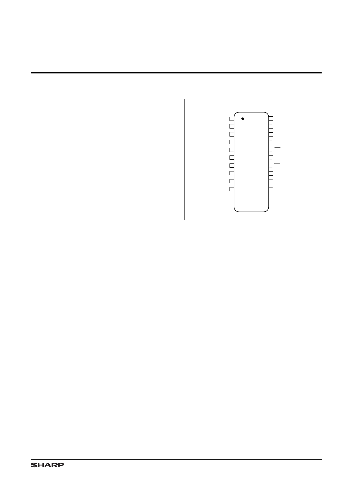
•• Packa ge: 24-pi n , 450 -mil SO P
DESCRIPTION
The LH5116S is a static RAM organized as 2,048 × 8
bits. I t is fab rica ted usin g sili con-gate CMOS process
technology. It operates at a low supply voltage of
3 V ±10%.
PIN CONNECTIONS
1
2
3
4
5
6
9
10
A
0
A
3
V
CC
24
23
22
21
20
19
16
15
A
5
A
4
7
8
A
1
A
2
18
17
A
7
A
6
OE
I/O
1
GND
A
8
A
9
A
10
CE
11
12
14
13
TOP VIEW
I/O
2
I/O
3
I/O
7
I/O
6
I/O
5
I/O
4
I/O
8
WE
5116S-1
24-PIN SOP
Figure 1. Pin Connections for SOP Package
1
TRUTH TABLE
CE OE WE MODE I/O1 - I/O
8
SUPPLY CURRENT NOTE
L X L Write D
IN
Operating (ICC)1
L L H Read D
OUT
Operating (ICC)
H X X Deselect High-Z Standby (I
SB
)1
L H X Output disable High-Z Operating (I
CC
)1
NOTE:
1. X = H or L
I/O
8
A
8
A
9
A
10
23
22
19
9
13
16
5116S-2
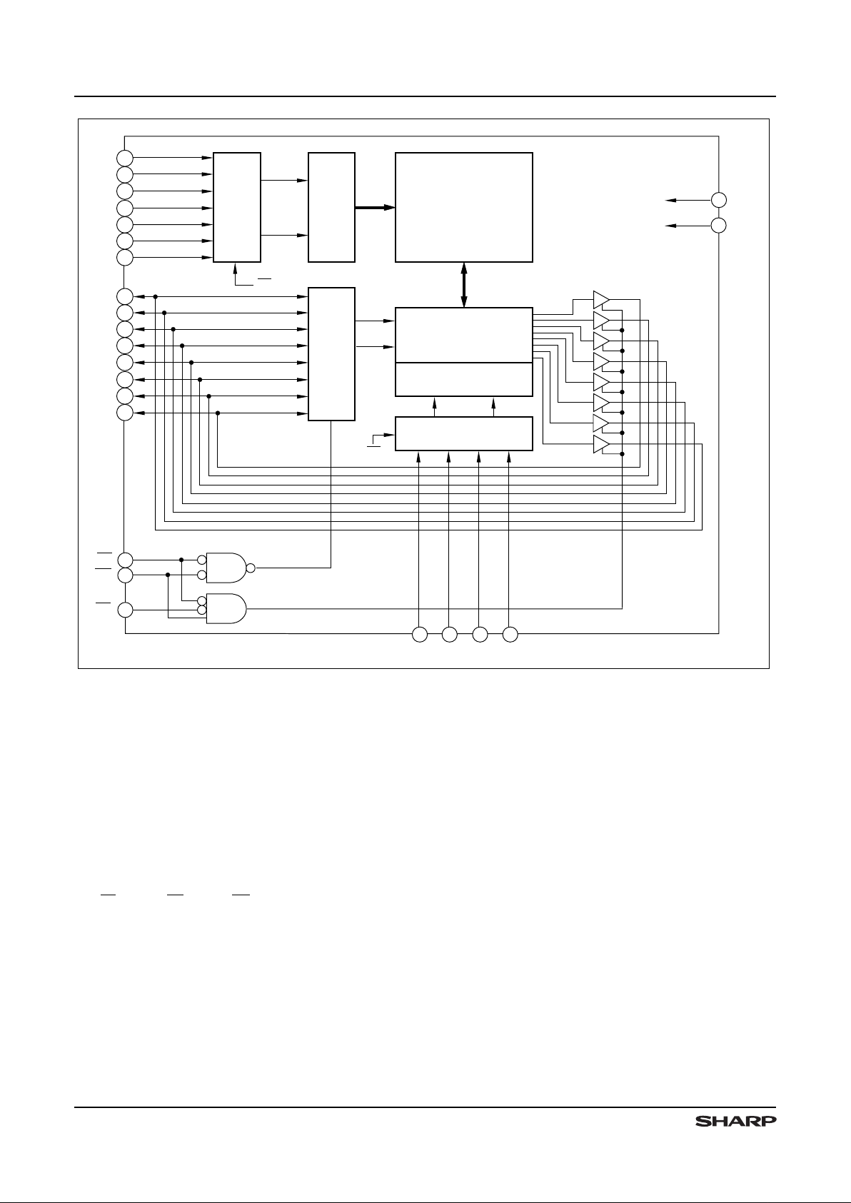
MEMORY CELL
ARRAY
(128 x128)
11
21
15
10
14
A
7
1
WE
ROW ADDRESS
BUFFERS
CE
A
6
2
A
5
3
18
A
0
8
ROW DECODERS
COLUMN
I/O CIRCUITS
COLUMN DECODERS
OE
DATA CONTROL
V
CC
GND
I/O
7
I/O
6
I/O
5
I/O
4
I/O
3
I/O
2
I/O
1
20
17
COLUMN ADDRESS
BUFFERS
4
A
4A3A2A1
7
5
6
24
12
CE
CE
Figure 2. LH5116S Block Diagram
PIN DESCRIPTI ON
SIGNA L PIN N AME
A0 - A
10
Addre ss input
CE Chip Ena ble in put
OE Outpu t E nab le inp ut
WE Wri te E na ble inp ut
SIGNAL PIN NAM E
I/O1 - I/O
8
Data i npu t/o utp ut
V
CC
Power sup ply
GND Ground
LH5116S CMOS 16K (2K × 8) Static RAM
2

ABSOLUTE MAXIMUM RATINGS
PARAMETER SYMBOL RATING UNIT NOTE
Suppl y v olt age V
CC
-0.3 to +7.0 V 1
Input vol tage V
IN
-0.3 to VCC +0.3 V 1
Operating temperature Topr 0 to +50
°C
Storag e t emp era ture Tstg -55 to +150
°C
NOTE:
1. The maximum appl icable vol tage on any pin with respect to GND.
RECOMMENDED OPERATING CONDITIONS (TA = 0 to +50°C)
P A RAMETER SYMBOL MIN. TYP. MAX. UNIT
Suppl y v olt age V
CC
2.7 3.0 3.3 V
Input vol tage
V
IH
2.2 VCC + 0.3 V
V
IL
-0.3 0.8 V
DC CHARACTERISTICS (VCC = 3 V ± 10%, TA = 0 t o +50°C)
PARAMETER SYMBOL CONDITIONS MIN. TYP. MAX. UNIT NOTE
Output ‘L OW’ v olta ge V
OL
IOL = 2.1 mA 0.5 V
Output ‘H IGH ’ vol tage V
OH
IOH = -1.0 mA
V
CC
- 0.5 V
Input lea kag e c urr ent I
LI
VIN = 0 V to V
CC
-1.0 1.0
µA
Output le aka ge cur ren t I
LO
CE = VIH, V
I/O
= 0 V to V
CC
-1.0 1.0
µA
Operat ing cu rre nt
I
CC1
Outputs open (OE = VCC) 8 10 mA 1
I
CC2
Outputs open (OE = VIH) 8 10 mA 2
Standb y c urr ent I
CCL
CE ≥ VCC - 0.2 V
All other input pins = 0 V to V
CC
1.0
µA
NOTES:
1. C E = 0 V; all other input pins = 0 V to V
CC
2. CE = VIL; all other input pins = VIL to V
IH
AC CHARACTERISTICS (VCC = 3 V ± 10%, TA = 0 t o +50°C)
(1) READ CYCLE
PARAMETER SYMBOL MIN. TYP. MAX. UNIT NOTE
Read c yc le t ime t
RC
1000 ns
Addres s a cc ess ti me t
AA
1000 ns
Chip e nab le acc es s ti me t
ACE
1000 ns
Chip e nab le Low to ou tpu t in Lo w-Z t
CLZ
10 ns 1
Output en abl e a cce ss tim e t
OE
100 ns
Output en abl e L ow to o utp ut in Low -Z t
OLZ
10 ns 1
Chip d isa ble to ou tpu t i n Hi gh- Z t
CHZ
040ns1
Output en abl e t o ou tpu t i n H igh -Z t
OHZ
040ns1
Output ho ld time
t
OH
10 ns
NOTE:
1. Active out put to high-impedance and high-impedance to outp ut
active tests specified for a ±200 mV transition
from steady state levels into the test load.
CMOS 16K (2K × 8) Static RAM LH5116S
3
 Loading...