

Page 1
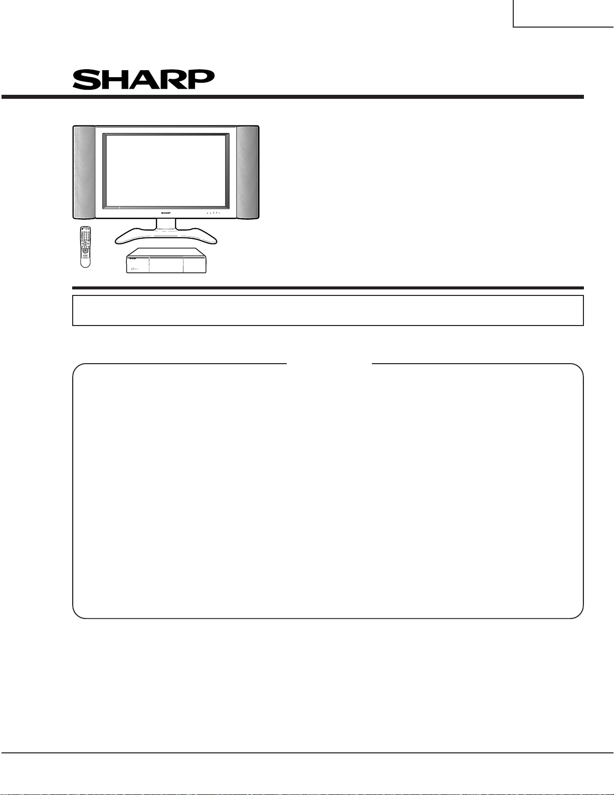
LC-30HV4M
LC-30HV4H
SERVICE MANUAL
S53B1LC30HV4M
LCD COLOUR TELEVISION
LC-30HV4M
MODELS
In the interests of user-safety (Required by safety regulations in some countries) the set should be restored
to its original condition and only parts identical to those specified should be used.
CONTENTS
Page
» IMPORTANT SERVICE SAFETY PRECAUTION .....2
» SPECIFICATIONS................................................4
» OPERATION MANUAL ........................................ 5
» DIMENSIONS ....................................................11
» REMOVING OF MAJOR PARTS........................13
»
ADJUSTMENT PROCEDURES (AVC System) ..
» UPGRADING INSTALLED PROGRAMS ...........28
» ADJUSTMENT PROCEDURES (Display) .........30
» MAJOR IC INFORMATIONS..............................34
» TROUBLE SHOOTING TABLE ..........................54
» CHASSIS LAYOUT.............................................64
» SYSTEM BLOCK DIAGRAM (AVC System) ......68
» SIGNAL FLOW BLOCK DIAGRAM
(AVC System).....................................................70
20
» POWER SYSTEM BLOCK DIAGRAM
(AVC System).....................................................72
» PC I/F BLOCK DIAGRAM (AVC System) ..........74
» SIGNAL BLOCK DIAGRAM (Display)................ 76
» POWER UNIT BLOCK DIAGRAM (Display) ...... 78
» OVERALL WIRING DIAGRAM (AVC System) ... 80
» OVERALL WIRING DIAGRAM (Display)............ 84
» DESCRIPTION OF SCHEMATIC DIAGRAM .....86
» SCHEMATIC DIAGRAM..................................... 87
» PRINTED WIRING BOARD ASSEMBLIES...... 163
» PARTS LIST .....................................................207
» PACKING OF THE SET ................................... 249
LC-30HV4H
Page
SHARP CORPORATION
Page 2
LC-30HV4M
2
2
2
2
LC-30HV4H
IMPORTANT SERVICE SAFETY PRECAUTION
Ë
Service work should be performed only by qualified service technicians who are thoroughly familiar with all safety checks and the servicing guidelines which follow:
WARNING
1. For continued safety, no modification of any circuit
should be attempted.
2. Disconnect AC power before servicing.
CAUTION: FOR CONTINUED PROTECTION
AGAINST A RISK OF FIRE REPLACE ONLY WITH
SAME TYPE FUSE.
AVC SIDE: F701 (T2AL, 250V).
LCD SIDE: F1 (T3.15AL, 250V), F3 (T2AL, 250V),
F6551, F6552, F6553, F6554, F6555, F6556
(T2.5AL, 250V)
BEFORE RETURNING THE RECEIVER
(Fire & Shock Hazard)
Before returning the receiver to the user, perform
the following safety checks:
1. Inspect all lead dress to make certain that leads are
not pinched, and check that hardware is not lodged
between the chassis and other metal parts in the
receiver.
2. Inspect all protective devices such as non-metallic
control knobs, insulation materials, cabinet backs,
adjustment and compartment covers or shields,
isolation resistor-capacitor networks, mechanical
insulators, etc.
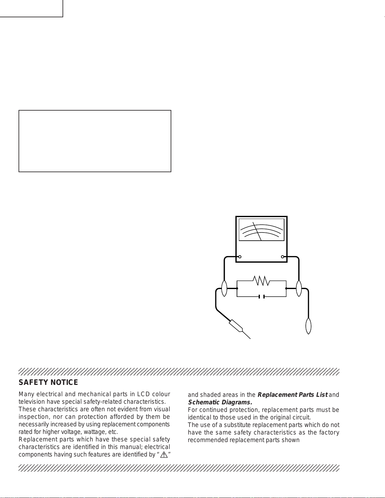
3. To be sure that no shock hazard exists, check for
leakage current in the following manner.
» Plug the AC cord directly into a 110~240 volt A C outlet.
» Using two clip leads, connect a 50k ohm, 10 watt
resistor paralleled by a 0.15µF capacitor in series
with all exposed metal cabinet parts and a known
earth ground, such as electrical conduit or electrical
ground connected to an earth ground.
» Use an AC voltmeter ha ving with 5000 ohm per v olt,
or higher, sensitivity or measure the A C v oltage drop
across the resisor.
» Connect the resistor connection to all exposed metal
parts having a return to the chassis (antenna, metal
cabinet, screw heads, knobs and control shafts,
escutcheon, etc.) and measure the AC voltage drop
across the resistor.
All checks must be repeated with the AC cord plug
connection reversed. (If necessary, a nonpolarized
adaptor plug must be used only for the purpose of
completing these checks.)
Any reading of 35V peak (this corresponds to 0.7
mA. peak AC.) or more is excessive and indicates a
potential shock hazard which must be corrected
before returning the monitor to the owner.
DVM
AC SCALE
50k ohm
10W
0.15 µF
TEST PROBE
TO EXPOSED
METAL PARTS
CONNECT TO
KNOWN EARTH
GROUND
234567890123456789012345678901212345678901234567890123456789012123456789012345678901234567890121
234567890123456789012345678901212345678901234567890123456789012123456789012345678901234567890121
SAFETY NOTICE
Many electrical and mechanical parts in LCD colour
television have special safety-related characteristics.
These characteristics are often not evident from visual
inspection, nor can protection afforded by them be
necessarily increased by using replacement components
rated for higher voltage, wattage, etc.
Replacement parts which have these special safety
characteristics are identified in this manual; electrical
components having such features are identified b y “ å”
234567890123456789012345678901212345678901234567890123456789012123456789012345678901234567890121
234567890123456789012345678901212345678901234567890123456789012123456789012345678901234567890121
and shaded areas in the
Replacement Parts List
Schematic Diagrams.
For continued protection, replacement parts must be
identical to those used in the original circuit.
The use of a substitute replacement parts which do not
have the same safety characteristics as the factory
recommended replacement parts shown in this service
manual, may create shock, fire or other hazards.
2
and
Page 3
LC-30HV4M
LC-30HV4H
Precautions for using lead-free solder
1 Employing lead-free solder
"PWBs" of this model employs lead-free solder. The LF symbol indicates lead-free solder, and is attached on the
PWBs and service manuals. The alphabetical character following LF shows the type of lead-free solder.
Example:
L Fa
Indicates lead-free solder of tin, silver and copper.
2 Using lead-free wire solder
When fixing the PWB soldered with the lead-free solder, apply lead-free wire solder. Repairing with conventional
lead wire solder may cause damage or accident due to cracks.
As the melting point of lead-free solder (Sn-Ag-Cu) is higher than the lead wire solder by 40°C, we recommend
you to use a dedicated soldering bit, if you are not familiar with how to obtain lead-free wire solder or soldening bit,
contact our service station or ser vice branch in your area.
3 Soldering
As the melting point of lead-free solder (Sn-Ag-Cu) is about 220°C which is higher than the conventional lead
solder by 40°C, and as it has poor solder wettabillty, you may be apt to keep the soldering bit in contact with the
PWB for extended period of time. However, since the land may be peeled off or the maximum heat-resistance
temperature of parts may be exceeded, remov e the bit from the PWB as soon as you confirm the steady soldering
condition.
Lead-free solder contains more tin, and the end of the soldering bit may be easily corroded. Make sure to turn on
and off the power of the bit as required.
If a different type of solder stays on the tip of the soldering bit, it is allo y ed with lead-free solder. Clean the bit after
every use of it.
When the tip of the soldering bit is blackened during use, file it with steel wool or fine sandpaper.
Be careful when replacing parts with polarity indication on the PWB silk.
Lead-free wire solder for servicing
Part No, ★ Description Code
ZHNDAi123250E J f0.3mm 250g(1roll) BL
ZHNDAi126500E J f0.6mm 500g(1roll) BK
ZHNDAi12801KE J f1.0mm 1kg(1roll) BM
3
Page 4
LC-30HV4M
LC-30HV4H
SPECIFICATIONS
Item 30 LCD COLOUR TV, Model:LC-30HV4H/M
LCD panel 30 Advanced Super View & BLACK TFT LCD
Number of dots 2,949,120 dots (1280
Video Colour System PAL/SECAM/NTSC 3.58/NTSC 4.43/PAL 60
TV
Function
Brightness 430 cd/m
Backlight 60,000 hours (at Save 1)
Viewing angles H : 170° V : 170°
Audio amplifier 10W
Speakers Ø 8 cm 2pcs
Terminals AV in, S-VIDEO in, COMPONENT VIDEO in
OSD language
TV-standard (CCIR)
Receiving
Channel
TV-Tuning System
STEREO/BILINGUAL NICAM/IGR
AVC
System
VHF/UHF
CATV
Rear INPUT 1
INPUT 2
INPUT 3
ANTENNA 75
MONITOR OUTPUT
DC OUTPUT DC 6.5V 7W MAX
Front
INPUT 4 AV in, S-VIDEO
PC
Headphones
PAL: B/G, D/K, I SECAM: B/G, D/K NTSC: M
44.25-863.25 MHz
Hyper-band, S1–S41ch
Auto Preset 99 ch, Auto Label, Auto Sort
2
2
AV in, S-VIDEO in
AV in, S-VIDEO in, COMPONENT VIDEO in
Din Type
Audio (Variable, Fixed), S-VIDEO out, VIDEO out
15 Pin mini D-Sub, Audio in (Ø 3.5mm jack)
Ø 3.5mm jack
English/Chinese/Arabic
768 3 dots)
Power Requirement
Power
Consumption
Weight
Accessories Operation manual, Remote control unit (
AVC System
Display
AVC System
Display
AC 110–240 V, 50/60 Hz
31 W (0.8W Standby)
104 W (0.6W Standby) (LC-30HV4H)/105W (0.7W Standby) (LC-30HV4M)
5.4 kg (w/o stand), 5.5 kg (with stand)
15.8 kg (w/o stand), 19.7 kg (with stand)
2), LR6 (“AA” size) Alkaline battery ( 2), Stand unit ( 1), Cable clamp
(
1), Antenna cable ( 1)
(
Specifications are subject to change without prior notice.
4
1), System cable ( 1), AC cord
Page 5
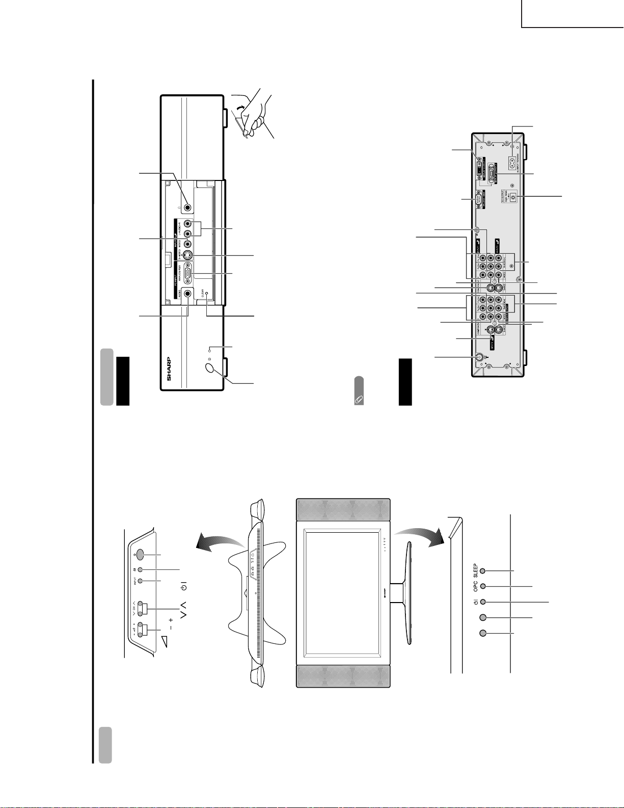
OPERATION MANUAL
Part names
OPC indicator*
STANDBY/ON indicator
(MAIN POWER)
OPC sensor
Display
(STANDBY/ON) button
INPUT
button
buttons
(
/
)
CH buttons (CH
/
)
Remote control sensor
*OPC: Optical Picture Control
Sleep timer
indicator
CLEAR*
POWER button
INPUT 4 terminal (S-VIDEO)
PC INPUT terminal (AUDIO)
INPUT 4 terminals (AUDIO)
PC INPUT terminal
(ANALOG RGB)
* If the AVC System is switched on but it does not appear to be operating correctly , it may need resetting. In this
case, press CLEAR, shown in the diagram, lightly with the end of a ballpoint pen or other pointed object.
This will reset the System as shown below.
• AV MODE resets to USER.
• TV channel resets to channel 1.
• Dual screen resets to normal.
• Audio setting initialises.
• SRS resets to OFF.
• Image position is initialised.
NOTE
• Pressing CLEAR will not work if the System is in standby mode (indicator lights red).
• Pressing CLEAR will not delete channel preset or password. See page 56 for clearing the password when you know it.
See page 66 for initialising to the factory preset values when you forget your password.
AVC System
STANDBY/ON indicator
INPUT 4 terminal (VIDEO)
(How to open the door)
Front view
Rear view
Headphone
(When connecting headphones,
the sound from the speakers is
muted.)
ANTENNA INPUT
terminal
INPUT 3
terminal
(S-VIDEO)
INPUT 3
terminal
(VIDEO)
INPUT 3
COMPONENT
VIDEO terminals
(Y, P
B
, P
R
)
INPUT 3 terminals
(AUDIO)
INPUT 1 terminal
(S-VIDEO)
INPUT 1 terminal
(VIDEO)
INPUT 1 COMPONENT
VIDEO terminals (Y, P
B
, P
R
)
INPUT 1 terminals
(AUDIO)
RS-232C terminal
DISPLAY OUTPUT 1
terminal
AC INPUT terminalDISPLAY OUTPUT 2
terminal
INPUT 2 terminals (AUDIO)
INPUT 2 terminal
(VIDEO)
INPUT 2 terminal (S-VIDEO)
MONITOR OUTPUT terminals (AUDIO)
MONITOR OUTPUT terminal (VIDEO)
MONITOR OUTPUT terminal
(S-VIDEO)
DC OUTPUT terminal (Terminal for
expanded functionality in the near future.)
LC-30HV4M
LC-30HV4H
5
Page 6
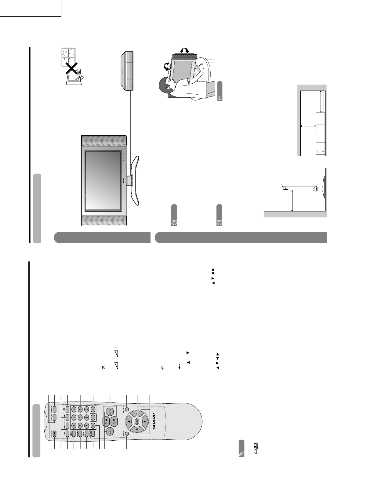
LC-30HV4M
Part names
1 POWER
To switch the power on and off.
2 FREEZE
Change the still image mode.
3 P&P
Set the dual picture mode. Press P&P again to return to normal view.
4WIDE
Change the wide image mode.
5 AV MODE
Select a video setting. AV MODE (STANDARD, DYNAMIC, MOVIE,
GAME, USER) PC MODE (STANDARD, USER)
6 MPX
Select the sound multiplex mode.
7 SURROUND*
Select SRS and FOCUS sound system.
8
(FLASHBACK)
Press to return to the previous channel in normal viewing mode.
9
/
(VOLUME)
Set the volume.
10 MENU
Display the menu screen.
11 DISPLAY
Display the channel information.
12 TV/VIDEO/PC
Select an input source. (TV, INPUT 1, INPUT 2, INPUT 3, INPUT 4,
PC)
13 SLEEP
Set the SLEEP TIMER.
14
(MUTE)
Mute the sound.
15 0 – 9
Set the channel.
16
(Digit for channel select)
Change the digits of the selected TV channel.
17 CH
/CH
Select the channel.
18 RETURN
Return to the previous menu screen.
19 ENTER
Execute a command.
Return to the initial image position after moving with
/
/
/
.
20
/
/
/
(Cursor)
Select a desired item on the setting screen.
Move the picture on the screen.
1
2
3
4
5
6
7
8
9
10
12
13
11
14
15
16
17
18
19
20
Remote control unit
NOTE
• When using the remote control unit, point it
at the Display.
*
is a trademark of SRS Labs, Inc.
FOCUS technology is incorporated under
license from SRS Labs, Inc.
Preparation
Where to place the System
“System” means the Display and AVC System. First select the location where to place the System.
1
2
Selecting the location of the System
• Select a place with no direct sunlight and good ventilation.
• The Display and the AVC System are connected by the system cable.
(See page 6 for details.)
Setting the System in place
Handling the Display
CAUTION
• Do not remove the stand from the Display unless using an
optional bracket to mount it.
• When moving, put your hands on the Display, but never on the
Display speakers.
• Keep enough space above and behind the Display.
Handling the AVC System
CAUTION
• Do not put a VCR or other device on the AVC System.
• Keep enough space above and on the sides of the AVC System.
• Do not block the ventilation openings on the top and left side,
and the exhaust fan on the right side.
• Do not spread a thick cloth beneath the AVC System, or cover it
with one, as this can cause overheating and result in
malfunction.
System cable
Display
AVC System
CAUTION
Adjust the screen with both
hands. Put one hand on the
Display and tilt the screen
while steadying the stand
with your other hand.
You can adjust the screen
vertically up to 10 degrees
forward or 8 degrees back-
ward, or rotate 10 degrees
horizontally.
5 cm or more
5 cm or more
on both sides
Keep enough space
There is an exhaust fan
on the right side.
10 cm
or more
LC-30HV4H
6
Page 7
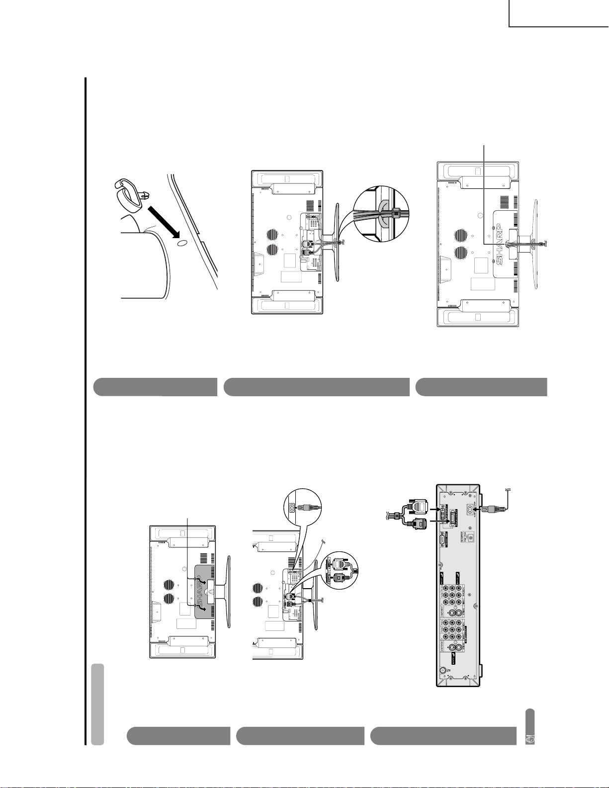
AC INPUT
110V–240V
DISPLAY INPUT2 DISPLAY INPUT1
System cable
AVC System (rear view)
AC cord
Display (rear view)
AC cord
System cable
(GREY)
Connect the plug firmly
until the hooks on both
sides click.
(WHITE)
Connect the plug into
the terminal and secure
it by tightening the
thumb screws.
(GREY) (WHITE)
Setting the System
After putting the Display and the AVC System in place, connect the system cables and AC cords. Use the
cable clamp for bundling the cables.
Preparation
Press down the two
upper hooks to remove
the cover toward you.
Connecting the system cable and the AC cord to the Display
1
2
3
Removing the terminal cover
Connecting the system cable and the AC cord to the AVC System
CAUTION
• TO PREVENT RISK OF ELECTRIC SHOCK, DO NOT TOUCH UN-INSULATED PARTS OF ANY CABLES WITH THE
AC CORD CONNECTED.
4
5
6
Attaching the clamp to the leg of the Display
Bundling the cables with the clamp
Closing the terminal cover
Display (rear view)
Cables come out from
the small opening.
LC-30HV4M
LC-30HV4H
7
Page 8
LC-30HV4M
Using external equipment
Display
(rear view)
HDTV tuner
AVC System
(rear view)
AVC System
(front view)
AV Receiver
(Built-in Tuner Amp)
VCR
Game console/Camcorder
PC
You can connect many types of external equipment to your System, like a VCR, DVD player, HDTV tuner, PC,
game console and camcorder. To view external source images, select the input source from TV/VIDEO/PC on
the remote control unit or INPUT on the Display.
CAUTION
• To protect all equipment, always turn off the AVC System before connecting to a VCR, DVD player, HDTV tuner , PC, game
console, camcorder or other external equipment.
NOTE
• Please refer to the relevant operation manual (DVD player, PC, etc.) carefully before making connections.
DVD player
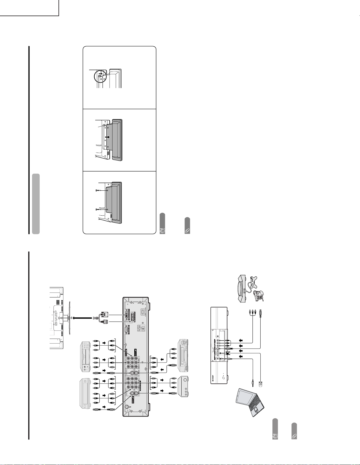
Using external equipment
Removing the speakers
This unit has detachable type speakers.
You can detach the system speakers when using external amplifier/speakers.
Before detaching (or attaching) speakers, unplug the AC cord from the AC outlet.
Before attaching/detaching speakers
• Before performing work, make sure to turn off the System.
• Before performing work, spread cushioning over a flat surface to lay the Display on. This will prevent it from
being damaged.
CAUTION
• The speaker terminals on the Display is only for the attached speakers. Do not connect any third party plug or speaker to
the terminal.
• Insert the speaker plug completely into the terminal.
• Do not handle or move the Display by the speakers.
NOTE
• Perform the same steps for both left and right speakers.
• To attach the speakers, perform the above steps in reverse order.
123
Unfasten the screws used to
secure the speakers in place.
Take hold of the speaker and
slowly slide it sideways.
(The speaker plug is still
inserted, so make sure not to
pull the speaker too far.)
Remove the speaker plug from
the terminal on the Display.
(Do not remove the plug by
pulling the cord.)
Now the speaker can be
detached from the Display.
Speaker
plug
LC-30HV4H
8
Page 9
Appendix
640
400
720
400
640
480
800
600
832
624
1024
768
1280
768
85 Hz
70 Hz
85 Hz
60 Hz
65 Hz
72 Hz
75 Hz
85 Hz
56 Hz
60 Hz
72 Hz
75 Hz
85 Hz
74.5 Hz
60 Hz
70 Hz
75 Hz
85 Hz
60 Hz
1280
1024 60 Hz
PC compatibility chart
Remarks
Macintosh 13" (67 Hz)
Macintosh 16"
Macintosh 19"
Resolution Frequency
Apple and Macintosh are registered trademarks
of Apple Computer, Inc.
DDC is a registered trademark of Video Electronics
Standards Association.
Power Management is a registered trademark of
Sun Microsystems, Inc.
VGA and XGA are registered trademarks of
International Business Machines Co., Inc.
RS-232C port specifications
Return codeCommand 4-digits Parameter 4-digits
PC Control of the System
• When a program is set, the display can be controlled from the PC using the RS-232C terminal.
The input signal (PC/AV) can be selected, the volume can be adjusted and various other adjustments and
settings can be made, enabling automatic programmed playing.
•
Attach an RS-232C cable cross-type (commercially available) to the supplied Din/D-Sub RS-232C for the
connections.
NOTE
• This operation system should be used by a person who is accustomed to using PCs.
Communication conditions
Set the RS-232C communications settings on the PC to match the display’s communications conditions. The
display's communications settings are as follows:
Baud rate:
Parity bit:
Data length:
Stop bit:
Flow control:
9,600 bps
8 bits
None
1 bit
None
Command format
Communication procedure
Send the control commands from the PC via the RS-232C connector.
The Display operates according to the received command and sends a response message to the PC.
Do not send multiple commands at the same time. Wait until the PC receives the OK response before sending
the next command.
Eight ASCII codes
CR
Command 4-digits:Command. The text of four characters.
Parameter 4-digits:Parameter 0 – 9, x, blank, ?
Parameter
Input the parameter values, aligning left, and fill with blank(s) for the remainder. (Be sure that four values are input for the
parameter.)
When the input parameter is not within an adjustable range,
“ERR” r
eturns. (Refer to “Response code format”.)
No problem to input any numerical value for
“x” on the table.
When “?” is input for some commands, the present setting value responds.
C1 C2 C3 C4 P1 P2 P3 P4
0055
100
– 30
0009
0
????
?
LC-30HV4M
LC-30HV4H
9
Page 10
LC-30HV4M
Commands
P
I
I
I
I
I
I
I
I
I
I
I
I
I
I
I
I
I
I
I
A
A
A
A
A
A
V
H
H
V
V
C
P
POWER OFF (STANDBY)
INPUT SWITCHING (TOGGLE)
TV (CHANNEL FIXED)
TV (CHANNEL SELECTION) (1
– 99)
INPUT1 – 4 (1 – 4)
PC
INPUT1 (AUTO)
INPUT1 (COMPONENT)
INPUT1 (S-VIDEO)
INPUT1 (VIDEO)
INPUT2 (AUTO)
INPUT2 (S-VIDEO)
INPUT2 (VIDEO)
INPUT3 (AUTO)
INPUT3 (COMPONENT)
INPUT3 (S-VIDEO)
INPUT3 (VIDEO)
INPUT4 (AUTO)
INPUT4 (S-VIDEO)
INPUT4 (VIDEO)
TOGGLE
STANDARD
DYNAMIC
MOVIE
GAME
USER
VOLUME (0 – 60)
H-POSITION (AV) (10– 10)
H-POSITION (PC) (90– 90)
V-POSITION (AV) (30– 30)
V-POSITION (PC) (60– 60)
CLOCK ( 90 – 90)
PHASE ( 20 – 20)
POWER SETTING
INPUT SELECTION A
INPUT SELECTION B
AV MODE
SELECTION
VOLUME
POSITION
O
T
T
T
A
P
N
N
N
N
N
N
N
N
N
N
N
N
N
N
V
V
V
V
V
V
O
P
P
P
P
L
H
W
G
V
V
V
C
P
P
P
P
P
P
P
P
P
P
P
P
P
P
M
M
M
M
M
M
L
O
O
O
O
C
S
R
D
D
D
D
D
1
1
1
1
2
2
2
3
3
3
3
4
4
4
D
D
D
D
D
D
M
S
S
S
S
K
E
0
x
0
*
*
x
0
1
2
3
0
1
2
0
1
2
3
0
1
2
0
1
2
3
4
5
*
*
*
*
*
*
*
_
_
*
_
_
_
_
_
_
_
_
_
_
_
_
_
_
_
_
_
_
_
_
_
*
*
*
*
*
*
*
_
_
_
_
_
_
_
_
_
_
_
_
_
_
_
_
_
_
_
_
_
_
_
_
_
*
*
*
*
*
*
_
_
_
_
_
_
_
_
_
_
_
_
_
_
_
_
_
_
_
_
_
_
_
_
_
_
_
_
_
_
CONTROL ITEM COMMAND PARAMETER
CONTROL
CONTENTS
W
W
W
W
W
W
W
W
W
W
W
W
S
S
S
S
S
T
T
D
C
C
TOGGLE
NORMAL
FULL 14:9
ZOOM 14:9
PANORAMA
FULL
CINEMA 16:9
CINEMA 14:9
NORMAL
FULL
DOT BY DOT
CINEMA
TOGGLE
OFF
SRS
FOCUS
SRS FOCUS
DUAL SCREEN OFF
DUAL SCREEN ON
DIRECT CHANNEL (1
– 99)
CHANNEL UP
CHANNEL DOWN
WIDE MODE
SURROUND
DUAL SCREEN
CHANNEL
I
I
I
I
I
I
I
I
I
I
I
I
R
R
R
R
R
W
W
C
H
H
D
D
D
D
D
D
D
D
D
D
D
D
S
S
S
S
S
I
I
C
U
D
E
E
E
E
E
E
E
E
E
E
E
E
S
S
S
S
S
N
N
H
P
W
0
1
2
3
4
5
6
7
8
9
1
1
0
1
2
3
4
0
1
*
x
x
_
_
_
_
_
_
_
_
_
_
0
1
_
_
_
_
_
_
_
*
_
_
_
_
_
_
_
_
_
_
_
_
_
_
_
_
_
_
_
_
_
_
_
_
_
_
_
_
_
_
_
_
_
_
_
_
_
_
_
_
CONTROL ITEM COMMAND PARAMETER
CONTROL
CONTENTS
Appendix
NOTE
• If an underbar (_) appears in the parameter column, enter a space.
• If an asterisk (*) appears, enter a value in the range indicated in brackets under CONTROL CONTENTS.
Return code (0DH)
Response code format
Normal response
Problem response (communication error or incorrect command)
Return code (0DH)
OK
ERR
Basic adjustment settings
AV input mode menu items
List of AV menu items to help you with
operations
Contrast
Brightness
Colour
Tint
Sharpness
Advanced
C.M.S.
Colour Temp
Black
Monochrome
Film Mode
I/P Setting
DNR
Picture
Power Save
No Signal Off
No Operation Off
Auto Installation
Programme Setup
Child Lock
Position
Full Mode
Rotate
Language
Treble
Bass
Balance
Surround
Input Select
Audio Out
Cool Climate
Colour System
Audio
Power Control
Setup
Option
PC input mode menu items
List of PC menu items to help you with
operations
Contrast
Brightness
Red
Green
Blue
C.M.S.
Picture
Power Save
Power Management
Input Signal
Auto Sync.
Fine Sync.
Rotate
Language
Audio
Power Control
Setup
Option
Treble
Bass
Balance
Surround
Audio Out
Cool Climate
LC-30HV4H
10
Page 11
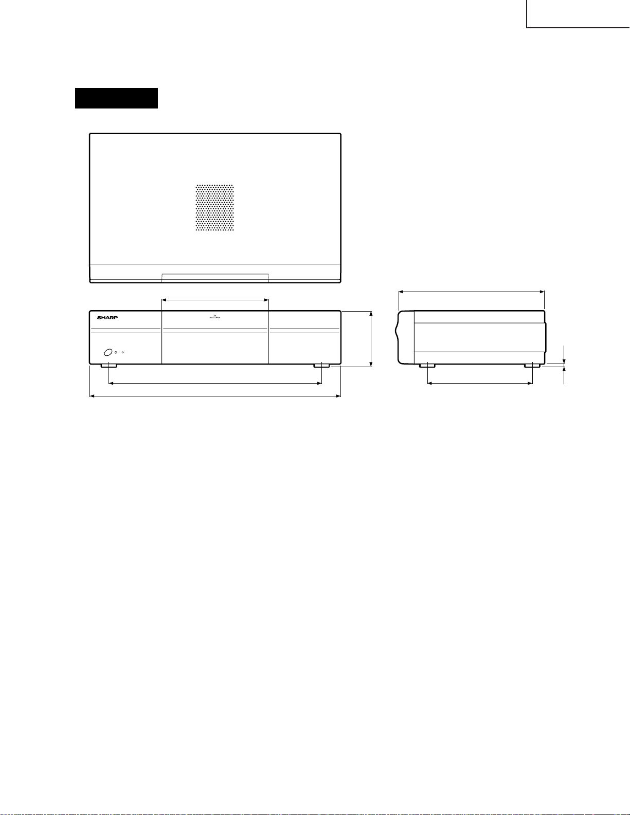
DIMENSIONS
365
430
250
5
180
95
183
Unit: mm
AVC System
LC-30HV4M
LC-30HV4H
11
Page 12
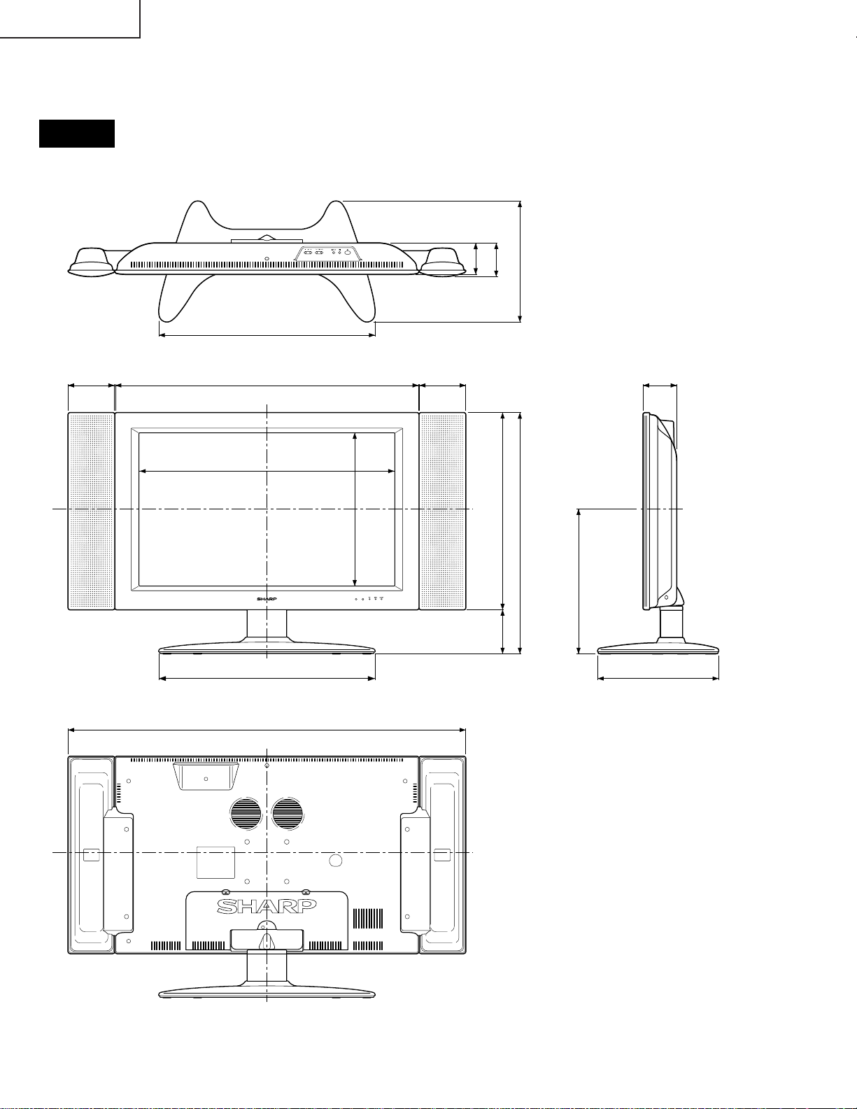
LC-30HV4M
LC-30HV4H
Display
545
117.5 117.5
643
766
Unit: mm
79
84.5
305608
84.5
497
545
1002
385
364
111
305
12
Page 13
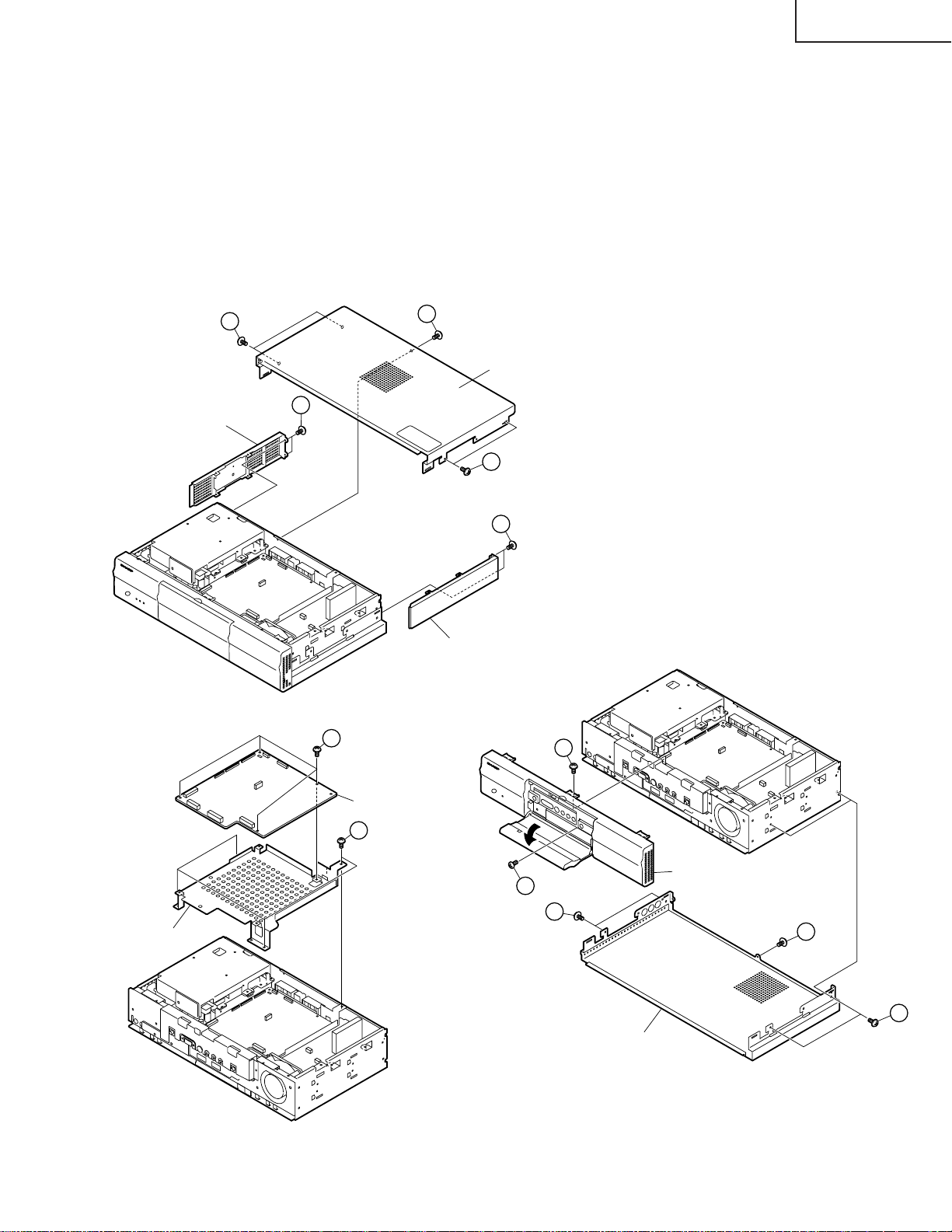
REMOVING OF MAJOR PARTS
Ë Ë
Ë AVC System
Ë Ë
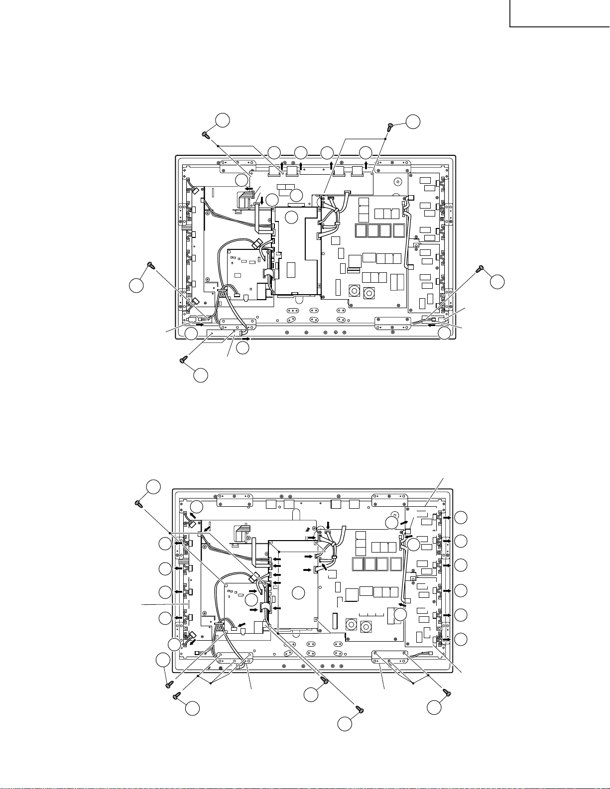
1. Remove the five top cabinet retaining screws and slide the top cabinet backward to remove it.
2. Remove the four side cover retaining screws on both the right and left sides and slide the side covers
backward to remove them.
3. Remove the one front panel retaining screws and remove the front panel.
4. Remove the five bottom cabinet retaining screws and slide the bottom panel backward to remove it.
5. Remove the four screws securing the main PWB angle and remove the angle upward.
6. Remove the four screws securing the main PWB to the angle and remove the main PWB.
LC-30HV4M
LC-30HV4H
1
Side Cover (L)
1
Top Cabinet
2
1
2
Side Cover (R)
6
3
Main PWB angle
Main PWB
5
Front panel
3
4
4
4
Bottom panel
13
Page 14
LC-30HV4M
LC-30HV4H
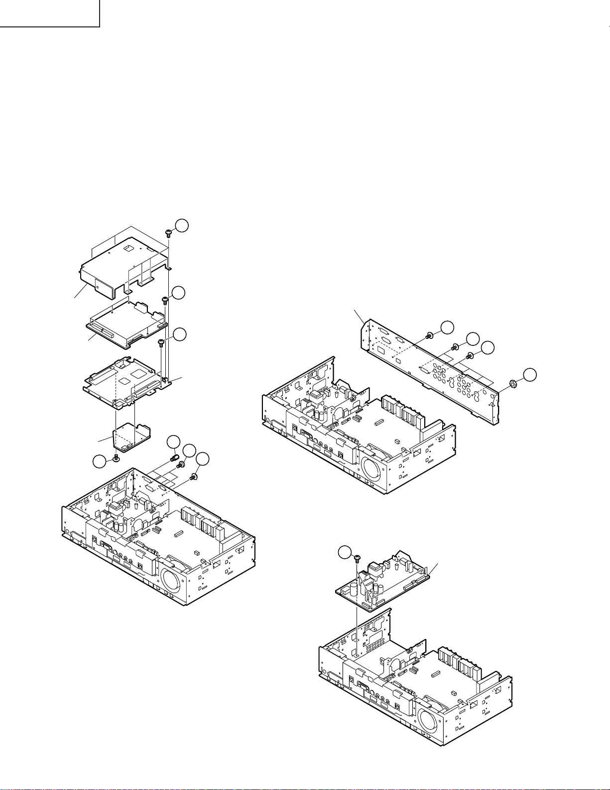
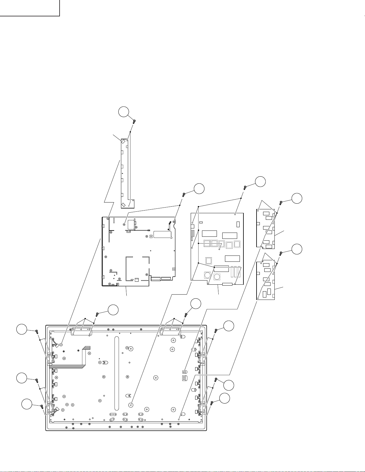
7. Remove the system/control terminal retaining:
7-1. Remove the four hex head screws securing the terminals of the system and control cables (white).
7-2. Remove the two screws securing the terminal of the system cable (gray).
7-3. Remove the two rear chassis retaining screws.
8. Remove the PC I/F and SR units:
8-1. Remove the six PC I/F top shield retaining screws and remove the shield.
8-2. Remove the six PC I/F unit retaining screws and remove the unit.
8-3. Remove the two PC I/F bottom angle retaining screws and remove the angle.
8-4. Remove the two SR unit retaining screws and remove the SR unit.
9. Remove the rear chassis.
9-1. Remove the one tuner nuts.
9-2. Remove the 10 rear cabinet retaining screws and remove the rear cabinet.
10. Remove the three power unit retaining screws and remove the power unit.
8-1
8-2
PC I/F Top Shield
Rear cabinet
PC I/F unit
SR unit
8-4
8-3
PC I/F Bottom Angle
7-1
7-2
7-3
10
9-2
9-2
9-2
9-1
Power unit
14
Page 15
11. Remove the AV unit:
Cooling Fan
12-1
11-1. Remove the five AV unit retaining screws and remove the AV unit.
11-2. Remove the three AV unit angle retaining screws and remove the angle.
12. Remove the fan:
12-1. Remove the two cooling fan retaining screws and remove the cooling fan.
13. Remove unit from the front chassis:
13-1. Remove the two hex head screws and four screws securing the front shield to the front chassis and
remove the front shield.
13-2. Remove the four screws securing the front unit and remove the unit.
11-1
AV unit
AV unit angle
11-2
LC-30HV4M
LC-30HV4H
13-1
13-1
Front Shield
13-2
Front unit
15
Page 16
LC-30HV4M
LC-30HV4H
Ë Ë
Ë Display
Ë Ë
1. Take off bottom terminal cover.
2. Take off the speaker by removing 4 screws and disconnecting speaker terminals.
3. Take off the table stand by removing 6 screws.
4. Take off the rear cabinet by removing 18 screws and releasing the front cabinet's 6 hooks.
Speaker
4
Rear Cabinet
4
4
Speaker
2
4
4
4
2
3
1
Terminal Cover
2
4
4
4
Table Stand
2
4
5. Take off the operation cover assembly by removing 2 screws and detaching the connector.
6. Take off the center angle by removing 8 screws and disconnecting 1 lead wire from the fan.
5
Operation Cover Ass'y
5
P131
P130
5
6
P2103
6
Center Angle
6
16
Page 17
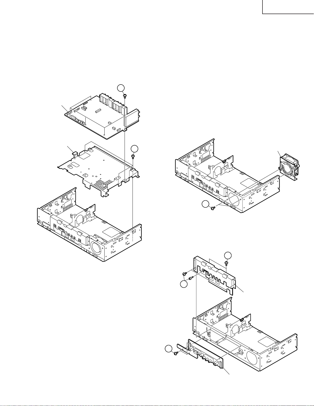
7. Take off the LCD control PWB by detaching 7 connectors and removing 4 screws.
8. Take off the R/C, LED PWB by detaching one connector and removing 2 screws.
9. Take off the speaker (L) PWB by detaching one connector and removing one screw.
10.Take off the speaker (R) PWB by detaching one connector and removing one screw.
LC-30HV4M
LC-30HV4H
9
Speaker(L)
PWB
P201
9
8
7
7
8
R/C,LED PWB
SC4502
SC4551
SC491
7
7
7
7
LCD
control
7
7
SC4503
7
13
Main
PWB
10
Speaker(R)
PWB
P202
10
11.Take off the main PWB by detaching 8 connectors and removing 4 screws.
12.Take off the audio PWB assembly by detaching 3 connectors and removing 4 screws.
13.Take off the 2 reinforcement angles by removing 3 screws from each angle.
14.Detach each connector.
Inverter-1 PWB
12
Inverter
GND PWB
14
14
14
14
14
P6901
P6902
P6903
P6904
P6905
P6906
P6907
Audio
PWB
P3804
P3802
12
P3801
P2106
SC2001
P2002
P2003
P2104
11
Main
PWB
CN4
P2101
P2102
CN5
CN3
Power Unit
14
CN7
14
P6565
14
P6564
P6551
P6553
P6555
P6558
P6560
P6562
14
12
Reinforcement angle
13
15
Reinforcement angle
13
11
14
14
14
14
14
14
Inverter 2 PWB
17
Page 18
LC-30HV4M
LC-30HV4H
15.Take off the inverter GND PWB by removing 2 screws.
16.Take off the power PWB by removing 7 screws. Remove insulation sheet.
17.Take off the inverter-1 PWB by removing 3 screws.
18.Take off the inverter-2 PWB by removing 3 screws
19.Take off the 4 reinforcement angles by removing 2 screws from each angle.
20.Take off the 2 reinforcement angles by removing 3 screws from each angle.
21.Take off the chassis frame by removing 2 screws.
22.Take off the LCD panel assembly by removing 2 screws.
15
Inverter GND
PWB
19
Chassis Frame
20
16
21
17
Inverter-1 PWB
18
Inverter-2 PWB
Power Unit
20
19
19
19
22
22
18
Page 19
LC-30HV4M
LC-30HV4H
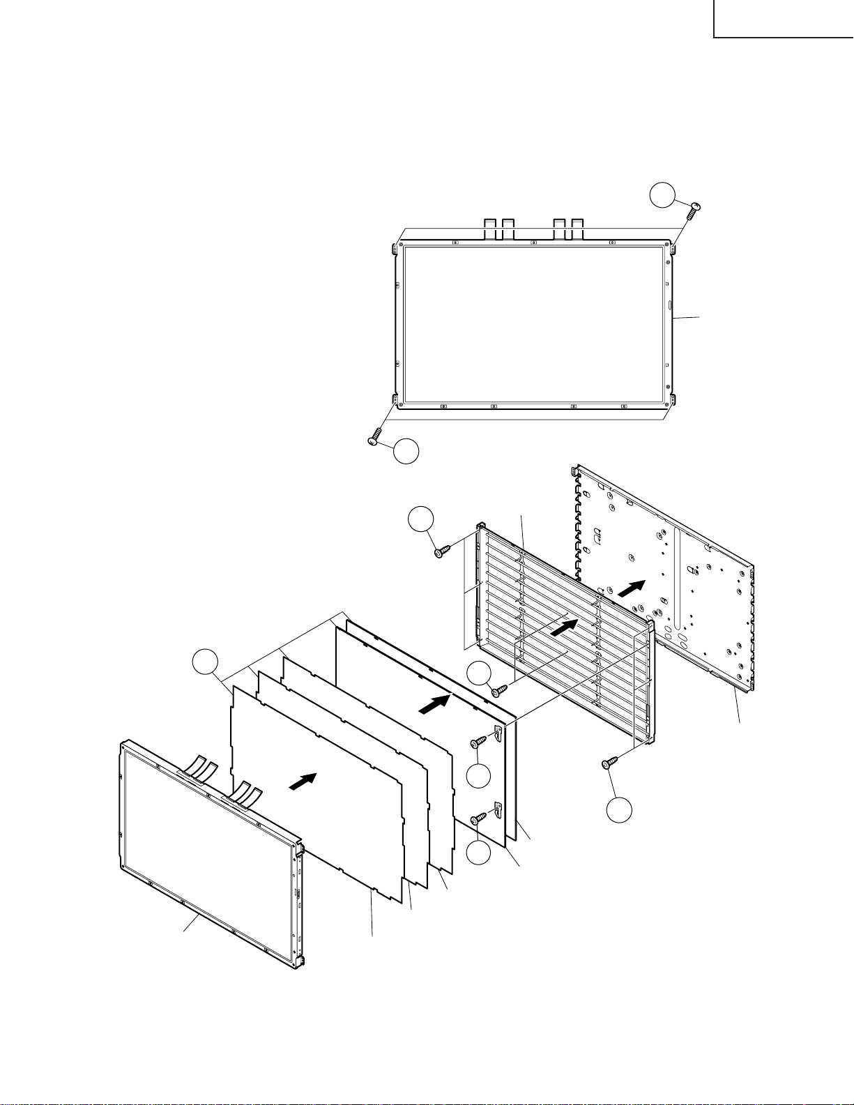
23.Take off the LCD panel with panel shield by removing 4 screws.
24.Take off D-BEF sheet, prism sheet and diffusion sheet. Take off ITO sheet and diffusion panel by removing 2
screws.
25.Take off the panel shield by removing 6 screws and 2 in the center.
23
LCD Panel
LCD Panel
24
23
25
Diffusion Sheet
Prism Sheet
D-BEF Sheet
25
24
24
Lamp
Panel Shield
25
Diffusion Panel
ITO Sheet
19
Page 20

LC-30HV4M
LC-30HV4H
ADJUSTMENT PROCEDURES (AVC SYSTEM)
Preparation for adjustment
1. The product has been adjusted and optimized in the factory. If the product needs to be readjusted for some
reason, e.g., after parts replacement, follow the instructions shown below.
2. Control parameter values set in the in-process adjustment mode has been stored in the corresponding registers.
When the product is readjusted, the contents of the registers are changed. Bef ore readjustment, f actory settings
should be noted in case the contents of registers require to be restored.
3. Use a stabilized AC power supply.
4. To rewrite a program, you should note the items ("OSD MENU" and "Adjustment Values") you want to change
and initialize EEPROM, and then rewrite the changes into EEPROM.
How to enter the in-process adjustment mode
CAUTION: Exercise great care to hide the procedure in entering the in-process adjustment mode from the
customer. Inadvertent setting changes in this mode may cause a fatal error resulting in a program being
unrecoverable.
1. Entering the in-process adjustment mode:
Connect the system cable between the display and AVC system. Connect the AC cord, respectively.
An AVC System is set as a standby state, and tur n off the "MAIN POWER" button of the Display.
Turn on the main power while holding down the "Input" button and the "VOL (-)" button of the Display
simultaneously. (Be continuing pushing "INPUT" and "VOL (-)" buttons until a display comes out.)
The system will be activated.
~If you see multiple lines of blue characters on the display, you are in the in-process adjustment mode. If not
(the normal activation screen opens), retry.
2. Accessing the inspection process mode:
After activation of the system, make adjustments according to the instructions indicated on the process
adjustment OSD menu screen.
Move to the General Process Adjustment (AVC System Section Process).
3. Restoring factory settings: (At the time of "INDUSTRY INIT" execution, please wait for about 30 seconds until
/// disappears.)
When the "INDUSTRY INIT" button is selected after activation of the system, factory channel setting remains
unchanged.
After the system exits from the in-process adjustment mode.
Changes made by the user will default to factory settings. Note that channel setting is also initialized.
4. Exiting from the in-process adjustment mode:
Unplug the power cable while the system is in the in-process adjustment mode to exit from the mode.
Take care not to press the "POWER" button on the remote controller or the AVC system after using factory
settings to run the system.
5. OSD menu screen and menu items during manual adjustment:
~The layout and men u items of the OSD menu screen ma y somewhat v ary depending on the program versions .
~Just rewriting a program does not cause settings to be "initial values". (Preparation for adjustment)
1. Button operation in the in-process adjustment mode
Cursor Up Move to the next page
Cursor Down Back to the previous page
Volume (Up) Increase the setting by 1
Volume (Down) Decrease the setting by 1
ENTER Execute the function
Cursor Left Increase the setting by 10
Cursor Right Decrease the setting by 10
Channel (Up) Move the cursor up
Channel (Down) Move the cursor down
INPUT Change input (Tuner -> Input 1 -> Input 2 ->Input 3 -> Input 4 -> PC ->)
20
Page 21
LC-30HV4M
CENTER Version
OSD Version
CVIC Version
TTXP Version
∫ ∫
∫ ∫
∫ ∫
∫ ∫
2001 06 21A
XXXXXXXX
XXXXXXXX
XXXXXXXX
∫
∫
∫
∫
Page Program version Color system
TUNER NO SIG1/19 HDCP:ON ASIA ASIA
Main unit AV unitHDCPSource of input
LC-30HV4H
2. In-process adjustment screen layout
6. Loading the backup data and setting HDCP when the PC I/F unit is replaced
Nearly all data including factory settings, user settings, and channel setting is stored in the PC I/F unit.
The product comes with EEPROM (IC1506) on the Main Unit in case the PC I/F unit is replaced; original data
backed up on the EEPROM can be loaded to the new PC I/F unit.
∫ How to load the backup data
Select EEPROM RECOVER in the OSD menu (page 19/19) and turn the "Volume" key ON; then press
"ENTER".
∫ How to set HDCP
After completion of adjustments, select KEY WRITE "ON" in the OSD men u (page 1/19) for manual adjustment
21
Page 22
LC-30HV4M
LC-30HV4H
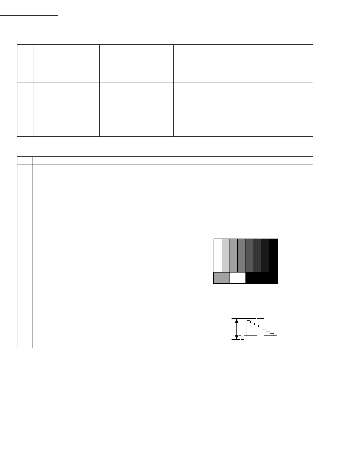
1) Analog adjustment
(1) V oltage adjustment
Item Adjusting conditions/points Adjusting procedure
1 3.3 V Adjustment Page: 1 » Connect a DC voltmeter to TP4 on the PC I/F unit.
Location: TP4
Move the cursor to
and (–)
keys to adjust the voltage to 3.30 ± 0.01 V.
"Ë
+Badj.3.3V" and use
2 1.8 V Adjustment Page: 1 » After adjustment to 3.3 V, move the cursor to the
Location: Pin (6) of CN9 "Ë+Badj.1.8V" line and press the "ENTER" key on
the remote controller. Adjustment will be made
automatically.
If "ERR" appears, adjust the voltage at pin (6) of
CN9 on the PC I/F unit to 1.90 ± 0.01 V.
(2) Tuner adjustment
Item Adjusting conditions/points Adjusting procedure
1 Signal setting Signal: 1.Set the colour system to PAL.
RF 2.Select the PAL source.
Split field color bar
» Split colour bar signal (100% white, colour 100%
Input pins: modulation)
ANT Input Terminal » With the video output open, make sure the voltage
is 2.0Vp-p (between sync level and 100% white
level).
» If the voltage is not as specified, readjust the signal
generator.
"VOL" (
+)
2 Tuner level Adjustment Connect the oscilloscope Provide the above RF signal to ANT and adjust
to TP1101.
"TUNER A DAC ADJ" so that the tuner output is
1.0 ± 0.02 Vp-p at TP1101.
1.0Vp-p
22
Page 23
(3) PAL signal adjustment
Adjustment items Adjustment conditions Adjustment procedures
1 Setup 1. Set colour system to PAL.
INPUT1-Video
2. Select PAL source.
100% colour bar signal including 100% white, such
as split field colour bar.
LC-30HV4M
LC-30HV4H
2 MAIN PAL Y
CONTRAST
adjustment
3 MAIN PAL COLOR
GAIN adjustment
4 MAIN PAL Cr GAIN
adjustment
5 MAIN CONTRAST
adjustment
6 SUB PAL Y
CONTRAST
adjustment
Pin (1) of P801
Pin (3) of P801
Pin (5) of P801
IC810 output (TP815)
Press the DUAL screen button. Select the special DUAL screen settings for adjustment
TB1274_SUB Output (TP806)
Adjust pin (1) of P801 to 0.70 ±0.025 Vp-p.
Adjust pin (3) of P801 to
0.70 ±0.025 Vp-p.
0.70V
Adjust pin (5) of P801 to
0.70 ±0.025 Vp-p.
0.70V
Adjust the output (TP815) of IC810 to have 0.90±0.025
Vp-p from the pedestal level.
(so that the same video source is reflected on MAIN/
SUB).
Adjust TB1274_SUB output (TP806) to
1.5 ±0.05 Vp-p.
7 SUB PAL COLOR
GAIN adjustment
TB1274_SUB Output (TP805)
Adjust TB1274_SUB output (TP805) to
1.5 ±0.05 Vp-p.
(4) SECAM signal adjustment
Adjustment items Adjustment conditions Adjustment procedures
1 Setup 1. Set colour system to SECAM.
2 MAIN SECAM Y
CONTRAST
adjustment
3 MAIN SECAM COLOR
GAIN adjustment
4 MAIN SECAM Cr
GAIN adjustment
INPUT1-Video
Pin (1) of P801
Pin (3) of P801
Pin (5) of P801
2. Select SECAM source.
100% colour bar signal including 100% white, such
as split field colour bar.
Adjust the "MAIN SECAM Y CONTRAST" setting so
that the 100% white level at Pin (1) of P801 should be
0.7±0.025 Vp-p.
Adjust "MAIN SECAM
COLOR GAIN" to 0.7 ±0.025
Vp-p at pin (3) of P801.
Adjust "GAIN MAIN SECOM
Cr " to 0.7 ±0.025 Vp-p at pin
(5) of P801.
0.7V
23
0.7V
Page 24
LC-30HV4M
LC-30HV4H
(5) N358 signal adjustment
Adjustment items Adjustment conditions Adjustment procedures
1 Setup 1. Set colour system to N358.
INPUT1-Video
2. Select N358 source.
100% colour bar signal including 100% white, such
as split fied colour bar.
2 MAIN N358 Y
CONTRAST
adjustment
3 MAIN N358 COLOR
GAIN adjustment
4 MAIN N358 Cr GAIN
adjustment
5 MAIN N358 TINT
adjustment
Pin (1) of P801
Pin (3) of P801
Pin (5) of P801
TB1274_MAIN Output (TP802)
Adjust "MAIN N358 Y CONTRAST" at 100% white
section to 0.70 ±0.025 Vp-p at pin (1) of P801.
Adjust "MAIN N358 COLOR
GAIN" to 0.70 ±0.025 Vp-p at
pin (3) of P801.
0.70V
Adjust "MAIN N358 Cr GAIN"
to 0.70 ±0.025 Vp-p at pin (5)
of P801.
0.70V
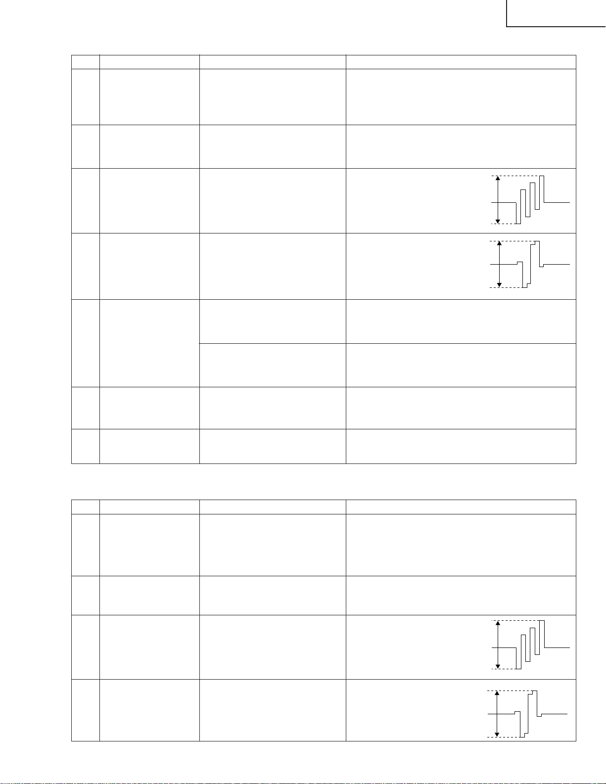
Adjust "MAIN N358 TINT" at TB1274_MAIN output
(TP802) so that waveform becomes as illustrated
below:
Smoothed
(6) Component 15k Hz signal adjustment
Adjustment items Adjustment conditions Adjustment procedures
1 Setup 1. Select component 15k Hz.
2 MAIN COMP 15k Y
CONTRAST
adjustment
3 MAIN COMP 15k
COLOR GAIN
adjustment
4 MAIN COMP 15k Cr
GAIN adjustment
INPUT1_COMPONENT
Pin (1) of P801
Pin (3) of P801
Pin (5) of P801
2. Select component source.
100% colour bar signal including 100% white, such
as split field colour bar.
Adjust "COMP 15k Y CONTRAST" to 0.70±0.025 Vp-p
at pin (1) of P801.
Adjust "COMP 15k COLOR
GAIN" to 0.70 ±0.025 Vp-p at
pin (3) of P801.
Adjust "COMP 15k Cr GAIN" to
0.70 ±0.025 Vp-p at pin (5) of
P801.
24
0.70V
0.70V
Page 25
(7) Component HDTV signal adjustment
Adjustment items Adjustment conditions Adjustment procedures
1 Setup 1. Input HDTV (1080i) component signal.
SIGNAL
∫ COMPONENT HDTV
∫ 100% Colour bar
POINT
INPUT1_COMPONENT
2. Select component source.
100% colour bar signal including 100% white, like
split field colour bar
LC-30HV4M
LC-30HV4H
2 MAIN COMP HDTV
CONTRAST
adjustment
Pin (9) of P801
Adjust the "COMP HDTV CONTRAST" at pin (9) of
P801 to have 0.90 ±0.025 Vp-p from the pedestal
level.
2. Factor y settings
Adjustment item Adjustment conditions Adjustment procedure
1 INDUSTRY INIT
* Then turn off the AC power supply of the AVC system. (Be careful not to use the power switches of the remote control unit
and DISPLAY unit.)
It will be an end, if unite cursor with the line of
"INDUSTRY INI", push a "VOL" button, it changes into
"ON", a "ENTER" button is pushed after that and it is
turned "OFF".
CAUTION:Before a setup is completed, please do not
shut off a power supply by any means.
Notes:
1) Perform factory setting as the latest task. Do not turn on the power after factory setting.
2) Turn the AVC ac po wer off to turn off the system.
Never turn off the power during factory setting.
3) After completion of factory setting, the system will exit from the process adjustment mode automatically. If not so,
HDCP has been set to off. Check HDCP setting.
4) Factory setting results in initializations of all user settings including channel setting.
(Items set in process adjustment mode are not initialized).
Items initialized by factory setting include the following:
∫ User settings (menu)
∫ Channel data (including broadcast frequencies)
∫ Password
∫ Operation time
∫ Auto installation flag
∫ Optimal manufacturer settings
25
Page 26
LC-30HV4M
LC-30HV4H
ËË
Ë Adjustment Mode Menu List (AVC System)
ËË
PAGE LINE NAME FUNCTION
11Ë+BAdj3.3V +BAdjust3.3VDisp(x,y,line)
21ËMAIN PAL Adjust AutoAdjustPAL_MAIN_Disp(x,y,line)
31ËSUB PAL Adjust AutoAdjustPAL_SUB_Disp(x,y,line)
41ËSECAM Adjust AutoAdjustSECAM_Disp(x,y,line)
51ËN358 Adjust AutoAdjustN358_Disp(x,y,line)
61ËCOMP15K Adjust AutoAdjustComp15k_Disp(x,y,line)
71ËPAL White Balance PAL_WB_Disp( x, y, line )
81ËN358 White Balance N358_WB_Disp( x, y, line )
2 Ë+BAdj1.8V(Enter:Auto) +BAdjust2.5VDisp(x,y,line)
3 KEY WRITE KeyWrite_Disp(x,y,line)
4 ËDATA COPY DataCopy_Disp(x,y,line)
5 INDUSTRY INIT IndustryInit_Disp(x,y,line)
6 CENTER Version CenterVersion_Disp(x,y,line)
7 OSD Version OSDVersion_Disp(x,y,line)
8 CVIC Version CVICVersion_Disp(x,y,line)
9 TTXP Version TTXPVersion_Disp(x,y,line)
10 MONITOR Version MonitorVersion_Disp(x,y,line)
11 STANDBY TYPE StandbyType_Disp(x,y,line)
12 HOTEL MODE HotelMode_Disp(x,y,line)
2 ËPAL Y CONTRAST PALYContrast_Disp(x,y,line)
3 ËPAL COLOR GAIN PALColorGain_Disp(x,y,line)
4 ËMAIN CR GAIN PAL MainCRGainPal_Disp(x,y,line)
5 ËMAIN CONTRAST 15K MainContrast15K_Disp(x,y,line)
6 Center Acutime CenterAcutime_Disp(x,y,line)
7 RESET CenterAcutimeReset_Disp(x,y,line)
8 Monitor Acutime MonitorAcutime_Disp(x,y,line)
9 RESET MonitorAcutimeReset_Disp(x,y,line)
2 ËSUB PAL Y SUBPALY_Disp(x,y,line)
3 ËSUB PAL COLOR GAIN SUBPALColorGain_Disp(x,y,line)
4 ËTUNER DAC ADJ TurerA_DAC_Disp( x, y, line )
2 ËSECAM Y CONTRAST SECAMYContrast_Disp(x,y,line)
3 ËSECAM COLOR GAIN SECAMColorGain_Disp(x,y,line)
4 ËMAIN CR GAIN SECAM MainCRGainSECOM_Disp(x,y,line)
2 ËN358 Y CONTRAST N358YContrast_Disp(x,y,line)
3 ËN358 COLOR GAIN N358ColorGain_Disp(x,y,line)
4 ËMAIN CR GAIN N358 MainCRGainN358_Disp(x,y,line)
5 ËN358 TINT N358TINT_Disp(x,y,line)
6 ËREFERENCE Adjust AutoAdjustRef_Disp(x,y,line)
2 Ë
COMP15K Y CONTRAST
3 Ë
COMP15K COLOR GAIN
4 Ë
MAIN CR GAIN COMP15K
5 ËCOMP HDTV Adjust AutoAdjustHDTV_Disp(x,y,line)
6 Ë
COMP HDTV CONTRAST
7 Ë
COMP HDTV SUB BRIGHT
8 ËPEAK ACL SW PeakACLSW_Disp(x,y,line)
2 PAL R CUTOFF PALRCutoff_Disp(x,y,line)
3 PAL R DRIVE PALRDrive_Disp(x,y,line)
4 PAL G CUTOFF PALGCutoff_Disp(x,y,line)
5 PAL G DRIVE PALGDrive_Disp(x,y,line)
6 PAL B CUTOFF PALBCutoff_Disp(x,y,line)
7 PAL B DRIVE PALBDrive_Disp(x,y,line)
8 DYNAMIC GAMMA DynamicGamma_Disp(x,y,line)
9 SIGNAL INFO SignalInfo_Disp(x,y,line)
10 TTXP READ/WRITE TTXPReadWrite_Disp(x,y,line)
11 TTXP ADDRESS TTXPAddress_Disp(x,y,line)
12 TTXP DATA TTXPData_Disp(x,y,line)
13 TTXP ANSWER TTXPAnswer_Disp(x,y,line)
14 TTXP UPDATE TTXPUpdate_Disp(x,y,line)
15 TTXIPL UPDATE TTXPLUpdate_Disp(x,y,line)
16 ËMAIN SUBBRIGHT 15K MainSubBright15K_Disp(x,y,line)
2 PC White Balance PC_WB_Disp( x, y, line )
3 N358 R CUTOFF N358RCutoff_Disp(x,y,line)
4 N358 R DRIVE N358RDrive_Disp(x,y,line)
5 N358 G CUTOFF N358GCutoff_Disp(x,y,line)
6 N358 G DRIVE N358GDrive_Disp(x,y,line)
7 N358 B CUTOFF N358BCutoff_Disp(x,y,line)
9 N358 B DRIVE N358BDrive_Disp(x,y,line)
Comp15kYContrast_Disp(x,y,line)
Comp15kColorGain_Disp(x,y,line)
MainCRGainComp15k_Disp(x,y,line)
CompHDTVContrast_Disp(x,y,line)
CompHDTVSubBright_Disp(x,y,line)
26
Page 27
LC-30HV4M
LC-30HV4H
91Ë
10 1 Ë
11 1 TROUBLE RECORD1 TroubleRecord1_Disp(x,y,line)
10 TROUBLE RECORD4 TroubleRecord4_Disp(x,y,line)
11 ACUTIME TroubleAcutime4_Disp(x,y,line)
12 TEMP TroubleTemp4_Disp(x,y,line)
12
| OMIT
17
18 1 NOISE C TUNER CVIC2NoiseCTunerA_Disp(x,y,line)
19 1 DEBUG PRINT SW DEBUG_Level_SW_Disp( x, y, line )
COMP15K White Balance
2 COMP15K R CUTOFF Comp15KRCutoff_Disp(x,y,line)
3 COMP15K R DRIVE Comp15KRDrive_Disp(x,y,line)
4 COMP15K G CUTOFF Comp15KGCutoff_Disp(x,y,line)
5 COMP15K G DRIVE Comp15KGDrive_Disp(x,y,line)
6 COMP15K B CUTOFF Comp15KBCutoff_Disp(x,y,line)
7 COMP15K B DRIVE Comp15KBDrive_Disp(x,y,line)
COMP33K White Balance
2 COMPHDTV R CUTOFF CompHDTVRCutoff_Disp(x,y,line)
3 COMPHDTV R DRIVE CompHDTVRDrive_Disp(x,y,line)
4 COMPHDTV G CUTOFF CompHDTVGCutoff_Disp(x,y,line)
5 COMPHDTV G DRIVE CompHDTVGDrive_Disp(x,y,line)
6 COMPHDTV B CUTOFF CompHDTVBCutoff_Disp(x,y,line)
7 COMPHDTV B DRIVE CompHDTVBDrive_Disp(x,y,line)
2 ACUTIME TroubleAcutime1_Disp(x,y,line)
3 TEMP TroubleTemp1_Disp(x,y,line)
4 TROUBLE RECORD2 TroubleRecord2_Disp(x,y,line)
5 ACUTIME TroubleAcutime2_Disp(x,y,line)
6 TEMP TroubleTemp2_Disp(x,y,line)
7 TROUBLE RECORD3 TroubleRecord3_Disp(x,y,line)
8 ACUTIME TroubleAcutime3_Disp(x,y,line)
9 TEMP TroubleTemp3_Disp(x,y,line)
2 NOISE C INPUT1 CVIC2NoiseCInput1_Disp(x,y,line)
3 NOISE C INPUT2 CVIC2NoiseCInput2_Disp(x,y,line)
4 NOISE C INPUT3 CVIC2NoiseCInput3_Disp(x,y,line)
5 NOISE C INPUT4 CVIC2NoiseCInput4_Disp(x,y,line)
6 NR LEVEL CVIC2NrLevel_Disp(x,y,line)
2 PIC ADJ MAKER SELECT Pict_Adj_Maker_Select_Disp( x, y, line )
3 PIC ADJ KOUTEI SELECT Pict_Adj_Koutei_Select_Disp( x, y, line )
4 EEPROM SAVE E2PROMSave_Disp( x, y, line )
5 EEPROM RECOVER E2PROMRecover_Disp( x, y, line )
6 CENTER PROG UPDATE CenterProgUpdate_Disp(x,y,line)
Comp15K_WB_Disp( x, y, line )
CompHDTV_WB_Disp( x, y, line )
27
Page 28

LC-30HV4M
LC-30HV4H
UPGRADING INSTALLED PROGRAMS
Programs installed in the product are mainly divided into the following two categories:
∫ Main programs (for AVC system)
∫ Monitoring program (for display)
CAUTON: Exercise great care to hide the procedure in entering the in-process adjustment mode from the
customer. Inadvertent setting changes in this mode may cause a fatal error resulting in a program being
unrecoverable.
[Tools required]
∫ PC
A Windows 95/98/me/2000/XP PC that has a COM port (RS-232C).
A USB-R232C converter will be acceptable provided that it is appropriately set and has PC compatibility.
∫ RS-232C cross cable
Interlink cable is also acceptable.
[Preparations]
Rewriting a program needs the product to enter the in-process adjustment mode.
1) The rewriting software is supplied in the form of an exe file named e.g., "MAIN_2002_10_10A.e x e" (provisional).
Create a directory on a HD and copy the software into the directory.
2)Double-click the file. The file will be self-extracted. Check the extracted file against the documentation
accompanying with the software.
3) Connect the AVC System and the display unit with each other and make them ready for operation (make sure
the power LEDs of the AVC System and display unit turn red).
4) Use an RS-232C cable to connect the PC to the AVC System.
5) Turn off the "MAIN POWER" button of the Display.
6) Press the "MAIN POWER" button while holding down the "VOL (-)" and "INPUT" buttons on the display unit
simultaneously. (Be continuing pushing "VOL (-)" and "INPUT" buttons until a display comes out.)
If blue characters appear on the display, the system has entered the in-process adjustment mode successfully.
If not (the normal activation screen opens), retry.
[Rewriting the main program]
1) In the in-process adjustment mode, press the "CH (Up)" button on the remote controller . You will move to page
("13/13" will appear on the upper left corner of the screen).
2) Make sure CENTER PROG UPDATE on page 1/19 is highlighted.
(It checks that "CENTER PROG UPDATE" on page 1/19 is chosen.)
3) Use the "VOL (+)/(-)" butons to change OFF to ON.
4) Press the "ENTER" button on the remote controller. Characters on the screen will disappear and the screen
blacks out.
5) Double-click the batch file specified in the document accompanying with the software.
6) A black window (MS-DOS window) will open and rewriting starts automatically.
For a while, "ok received" will appear on the screen.
Rewiring of the main program is now complete. Unplug the AC cord from the AVC System and turn off the
system and then on again.
7) Enter the in-process adjustment mode and make sure the version information on the "CENTER Version",
"OSD Version" and "CVIC Version" lines on page 1/19 has been updated.
28
Page 29
LC-30HV4M
LC-30HV4H
Continued
29
Page 30

LC-30HV4M
LC-30HV4H
ADJUSTMENT PROCEDURES (DISPLAY)
See "Adjusting mode" for the steps to go into adjustment process mode.
NOTE: When IC2203 is replaced, it id needed to initialization first then Background adjustment and Common bias
adjustment.
1) +B adjustment (LCD Control PWB: R4648)
1. Receive NTSC standard color bar signal.
2. Connect digital voltmeter to TP4602 and adjust to the specified value.
Specification: 13.00 ± 0.05V
2) Common bias adjustment
Make this adjustment each for "50 Hz", "60 Hz" and "PC". Select the input signal according to the indication onscreen.
1. Go to "Adjustment process mode".
2. On the LCD, select "14" of "PATTERN 1", dot inversion flicker pattern 2.
3. Then, select "COM BIAS" on the LCD.
4. Set the value so that the flicker on the screen is minimized.
Note: Apply this adjustment after for at least 30 min.
3) Background adjustment
1. Select video standard, and confirm the indication that the unit is preset to the standard.
2. At video input, receive the window pattern signal having left 80% WHITE (200/255) and right 20% WHITE (48/
255).
3. Set the screen size to the full mode.
4. Go to "Adjustment process mode".
5. Adjust "R OFFSET", "G OFFSET" and "B OFFSET" in "SIL861" so that left side 80% WHITE window pattern is
set to the specified value.
6. Adjust "R GAMMA", "G GAMMA" and "B GAMMA" in "SIL861" so that right side 20% WHITE window pattern is
set to the specified value.
Specification: x = 0.278, y = 0.274 (80% WHITE), x= 0.259, y = 0.248 (20% WHITE) (LC-30HV4M)
x = 0.283, y = 0.274 (80% WHITE), x= 0.263, y = 0.242 (20% WHITE) (LC-30HV4H)
Note: Apply this adjustment after for at least 30 min.
4) Initialization
1. Go to "Adjustment process mode".
2. Select "1" thru "3" of "CLR MODE" in "TEST".
Setting range: 0 Normal
1 Initial setting (User clear: Factory setting)
2 Initial setting (All clear) Full initialization of EEPROM (except for ROM area)
3 Full initialization of Configuration EEPROM
3. Move the cursor down by one line.
4. Press "VOL UP" key and change the display from "WAIT" to "SEND" (write).
5. Do not shut down power while the display is "SEND".
6. When the writing is finished, the display changes from "SEND" to "WAIT".
5) Resetting lamp error counter
1. Go to "Adjustment process mode".
2. Select "L ERR RESET" in "TEST".
3. Reset the data to "0".
[L ERR RESET]
Function: Reset of fluorescent lamp error counter
It resets the times of fluorescent lamp errors and clears the last value in the memory.
Indication range: 0-5 (Fluorescent lamp errors)
(When lamp error exceeds 5 times, power supply is disabled. Resetting is required in this case.)
30
Page 31

LC-30HV4M
LC-30HV4H
3.
Adjusting Mode
1. Overview
The controller IC can be adjusted in this mode.
Adjustment is done while controlling the setting of the resistor corresponding to the selected adjustment item.
When monitor is used independently, it is adjusted using the OSD simple display function incorporated in LCD
controller.
The OSD function of panel link receiver (SIL861) is used for adjustment of the independent monitor.
2. Entry to the mode
1) When cable is not connected (independent mode), follow the steps below.
a) When power switch is turned on, press the main unit INPUT and VOL DOWN keys simultaneously.
b) Press the remote controller's process adjustment key (R/C code: 40h) / process adjustment mode 2 key (R/
C code: 31h).
2) When not in independent mode, follow the steps below.
a) When power switch is turned on, press the main unit CH DOWN and VOL UP keys simultaneously.
b) Press the remote controller's process adjustment mode 2 key.
3. Exit from the mode
Turn off the power.
Press the remote controller's process adjustment mode 2 key.
4. Display
1) First layer display
The third line shows the title. The 5th line and below show the items. Microprocessor's version number
appears in the 16th line.
Example) 1.00 Æ 1 00
1234567891011121314
1SERVICE MODE
2OMODE 50HZ
3LCD
4SIL861
5TEST
6VERXXX
2) Second layer display (Adjustment item display)
A single page shows up to 10 adjustment items (or 14 lines).
The third line shows the title and the screen mode selected in MODE items (only when LCD is selected).
The 5th line shows the item. Microprocessor's version number appears in the 16th line.
Example) 1.00 Æ 1 00
Setting is shown in decimal number.
a) Adjustment on the LCD items
1234567891011121314
1LCD 50HZ
2OVL0 22 1
3REF0 209
4VL64 98
5REF64 170
6VL96 92
7REF96 184
8 VL128 85
9REF128 188
10 VL160 71
11 REF160 199
31
Page 32

LC-30HV4M
LC-30HV4H
b) Adjustment on the TEST items
1234567891011121314
1TEST
2OL ERR RE 0
3LCDDATA0000
4WAIT
5CLRMODE 0
6WAIT
7CNFGEEP0000
8WAIT
5. Changing data
In "adjustment item display", the items pointed by cursor can be changed using VOL UP/DOWN key.(Holding
down the key is effective.)
For the items in "LCD DATA", select the item and hit ENTER key. The ten's digit (leftmost digit) in the address
changes to red (others in green). Data change using VOL UP/DOWN key is enabled.
To move to the next digit, press CH UP k ey (or rightward cursor k e y). To go back to the previous digit, press CH
DOWN key (or leftward cursor key). Thus, 4 digits data can be entered.
When CH UP key is pressed while in rightmost digit, the cursor moves to the leftmost digit. When CH DOWN
key is pressed while in leftmost digit, the cursor moves to the rightmost digit.
After address data adjustment, press ENTER key to exit from 4-digit adjustment and change the entire "LCD
DATA" line to red letters. (Same status as item selection)
6. Key operation
1) Basic behaviors
Basic key behaviors are as follows.
Behavior Keys
Remote controller Main unit
Upward cursor movement Cursor up CH UP
Downward cursor movement Cursor down CH DOWN
Rightward cursor movement Cursor right
Leftward cursor movement Cursor left
Data UP VOL UP VOL UP
Data DOWN VOL DOWN VOL DOWN
Set ENTER INPUT
Back to previous layer RETURN
Back (In bottom layer only) ENTER INPUT
2) Data UP/DOWN
For the item for which OSD display is available, switch the display.
Adjust the data with UP/DOWN operation. (Any value beyond the limit is replaced by the limit value.)
Output data processing
Data transmission for every UP/DOWN operation (Data related to peripheral controller IC)
Execution of the last memory data when key is off
While the key is held down, the second step is performed approx. 500ms after the k ey operation and, after this,
every single step of UP/DOWN is carried out sequentially at 135ms interval.
3) Cursor UP/DOWN
Select the adjustment item by pointing it with the cursor.
When upward cursor movement is done while the cursor is at the top item, the cursor goes to the bottom item.
(In the case of multiple pages, the cursor goes to the bottom item on the previous page.)
When downward cursor movement is done while the cursor is at the bottom item, the cursor goes to the top
item. (In the case of multiple pages, the cursor goes to the top item on the next page.)
While the key is held down, the second step is performed approx. 500ms after the k ey operation and, after this,
every single step of UP/DOWN is carried out sequentially at 135ms interval.
32
Page 33

ËË
Ë Adjustment Mode Menu List (Display)
ËË
First layer item PAGE ITEM SETTING RANGE INITIAL VALUE DATA SETTING
MODE 1 50HZ/60HZ/PC 50HZ Toggle
LCD 1 VL0 0 ~ 255 221 No Toggle
REF0 0 ~ 255 209 No Toggle
VL64 0 ~ 255 98 No Toggle
REF64 0 ~ 255 170 No Toggle
VL96 0 ~ 255 92 No Toggle
REF96 0 ~ 255 184 No Toggle
VL128 0 ~ 255 85 No Toggle
REF128 0 ~ 255 188 No Toggle
VL160 0 ~ 255 71 No Toggle
REF160 0 ~ 255 199 No Toggle
2 VL192 0 ~ 255 77 No Toggle
REF192 0 ~ 255 103 No Toggle
VL224 0 ~ 255 88 No Toggle
REF224 0 ~ 255 112 No Toggle
VL256 0 ~ 255 108 No Toggle
REF256 0 ~ 255 78 No Toggle
COM BIAS 0 ~ 255 70 No Toggle
PWM CTRL 0 ~ 7 Toggle
PWM FREQ 0 ~ 4095 585 No Toggle
PWM DUTY 0 ~ 4095 0 No Toggle
3 PATTERN1 0 ~ 14 0 Toggle
PATTERN2 0 ~ 12 0 Toggle
P – CLK1 0 ~ 3 0 No Toggle
P – CLK2 0 ~ 7 0 No Toggle
OS SW 0 ~ 1 0 Toggle
OS D1 0 ~ 255 138 No Toggle
OS D2 0 ~ 255 167 No Toggle
OS D3 0 ~ 255 170 No Toggle
OPC LV0 0 ~ 85 0(40) No Toggle
OPC LV1 0 ~ 85 8(44) No Toggle
4 OPC LV2 0 ~ 85 16(48) No Toggle
OPC LV3 0 ~ 85 24(52 )No Toggle
OPC LV4 0 ~ 85 32(56) No Toggle
OPC LV5 0 ~ 85 40(60) No Toggle
OPC LV6 0 ~ 85 48(64) No Toggle
OPC LV7 0 ~ 85 56(68) No Toggle
OPC LV8 0 ~ 85 64(72) No Toggle
OPC LV9 0 ~ 85 72(76) No Toggle
OPC LV10 0 ~ 85 80(80) No Toggle
SIL861 1 R GAMMA 20 ~ 180 100 No Toggle
R OFFSET 0 ~ 510 256 No Toggle
G GAMMA 20 ~ 180 100 No Toggle
G OFFSET 0 ~ 510 256 No Toggle
B GAMMA 20 ~ 180 100 No Toggle
B OFFSET 0 ~ 510 256 No Toggle
TEST 1 L ERR RESET 0 ~ 5 0 Toggle
LCD DATA Four digits 0 ~ F 0 Toggle
WAIT/SEND WAIT ———
CLR MODE One digits 0 ~ 2 0 Toggle
WAIT/SEND WAIT ———
CNFG EEP Four digits 0 ~ F 0 Toggle
WAIT/SEND WAIT ———
LC-30HV4M
LC-30HV4H
* Values in the parentheses are with PC.
33
Page 34

LC-30HV4M
LC-30HV4H
MAJOR IC INFORMATIONS
∫ IC2501 (MSP4458G)
IC for decoding audio signals.
It serves as an S-IF audio signal decoder and an audio data selector.
∫ IC2701 (IXA385WJ)
IC for controlling audio delay.
This model uses a frame buffer to process video signals . This results in a delay in outputting video signals. The
IC delays output of audio signals to synchronize output of video and audio signals.
∫ IC1301 (CXA2069Q)
7-input, 3-output selector.
This IC selects all audio and video signals received from input terminals and the tuner, except those signals
that relates to PC and components.
Video signals delivered to the IC are sent to Y/C separation circuits IC401 (main) and IC402 (sub). Audio
signals are sent to the SR unit via IC2501 (sound processor).
∫ IC1401 (MM1519XQ)
4-input, 3-output video selector for component input.
This IC receives AV3 component input, AV1/3 RGB input and teletext RGB signals. Its output is for main, sub
and component.
∫ IC1601 (SDA5550M) (Only for LC-30HV4M)
Teletext processing micro-processor.
This IC receives vide signals, decodes teletext and outputs data in RGB format.
∫ IC7001 (µPD64084)
This IC provides 3D processing of NTSC signals and thus high resolution Y/C separation of the main image
signals received from IC1301.
It incorporates a 4M-bit frame delay memory board and features one-chip 3D Y/C separation.
∫ Two operation modes available; dynamic image 3D Y/C separation mode and 2D Y/C separation + YCNR
mode
∫ Y coring circuit, vertical contour compensation circuit, peaking filter and noise detection circuit incorporated
∫ Power down mode available to minimize power consumption when not in operation
∫ IC401/IC402 (TC90A69)
Adaptive in-field comb filter supporting both the NTSC and PAL systems. Equipped with CNR circuit, the 3-line
digital comb filter is a high-precision Y/C single chip, which provides Y/C separation of sub image signals
received from IC1301.
∫ IC403/IC7003/IC404 (ML6428Cl)
6.7 MHz low-pass filter.
∫ IC801/802 (TB1274AF)
IC for synchronous processing of video and chroma signals for PAL/NTSC/SECAM colour TV.
Color demodulation is provided by a high-performance image compensation circuit in the video section, a
PAL/NTSC/SECAM auto discrimination circuit in the chroma section, and a crystal that generates 4.43 MHz,
3.58 MHz and M/N-PAL clock signals.
This IC has a 4-channel YC signal input, 2-channel RGB signal input, and 2-channel chrominance signal input.
It receives main and sub chrominance signals from IC401 (main) and IC402 (sub) and delivers chrominance
signals via one-channel output.
∫ IC803 (CXA2101Q)
IC having a chrominance input integrated with a high-perf ormance image compensation circuit. Equipped with
circuits for processing baseband signals and RGB signals and a 4-channel video switch incorporating an H/V
synchronization signal processing circuit.
Input selection is done by INPUT-SEL (IIC BUS). YCbCr, Y, PbPr, GBR and their H/V synchronization signals
are inputted to input pins of each channel.
Multi-scan facility permits acceptance of a horizontal scan line frequency range of 15 kHz to 60 kHz.
∫ IC1901 (IXA392WJ)
FPGA for synchronous processing.
This IC selects synchronization signals and creates horizontal blanking signals.
∫ IC604 (TA1318AF)
IC for synchronous processing of TV component signals and measurement of frequency.
This IC incorporates an input signal frequency measurement feature and synchronous regeneration features.
It supports synchronous horizontal regeneration (15.75 kHz, 31.5 kHz, 33.75 kHz and 45 kHz) and synchronous
vertical regeneration (480I, 480P, 576I, 720P, 1080I, PAL 100 Hz, and NTSC 120 Hz).
34
Page 35

LC-30HV4M
LC-30HV4H
∫ PC I/F unit
∫ IC10004 (CXA3506R)
3-ch, 8-bit 120MSPS A/D converter incorporating AMP and PLL.
This IC process video signals supplied to the interface board. On the main side, video signals (analog RGB)
from CN6 are inputted to IN1 of IC10004. On the PC side , vide signals (analog RGB) from CN8 are inputted to
IN2 of IC10004.
Converted digital signals are sent to IC10025.
∫ IC10310 (TLC5733A)
3-ch, 8-bit 20MSPS A/D converter.
This IC processes video signals supplied to the interface board. It receives analog signals (YCbCr) from CN6
and sends converted digital signals to IC10310.
The incoming video signal is converted to digital one and fed to IC10025.
∫ IC10025 (IXA091WJ)
IC for I/P conversion and scaling of digital image according to the output resolution, and for data conversion.
There are two input channels: V0 and V1. V1 is for sub 480i input processing for two-screen application. V0 is
for processing all signals for main used for one and two-screen applications.
∫ The IC generates clamp signals based on input synchronization signals.
∫ It also performs data matrix conversion.
∫ It creates OSD signals.
The incoming video signal is fed to IC10413.
∫ IC10413 (SII170)
Panel link transmitter.
This IC converts 8-bit RGB image data received from IC10025 into TMDS differential signals and sends the
resulting digital signals to the monitor.
HDCP function is provided.
∫ IC10001 (IX3270CE)
One-chip RISC microprocessor.
This IC communicates with the monitor and controls the system operation.
It controls all the ICs located in the AVC system.
∫ IC10405 (µPD4721G)
RS-232 line driver/receiver conforming to EIA/TIA-232-E.
This IC enables the system to be controlled from a PC connected to the system.
It also allows IC10001 to be upgraded using the PC.
35
Page 36

LC-30HV4M
LC-30HV4H
ËRH-iXA385WJZZ (ASSY:IC2701)
DELAY
» Pin mapping
Pin No. Pin Name Type Description
1, 19, 32, 33 VDD –– Power supply
44, 64
2 PLLVDC –– PLL power supply
3 VCOIN I VCO IN (used to construct external loop filter)
4 TEST I Input for testing
5 CPOUT O Charge pump out (used to construct external loop filter)
6 PLLEN I PLL enable signal input
7 PLLGND ––
8, 9, 10, 18, 31 GND ––
41, 42, 43, 62
11 PLLENO O PLL enable signal output
12 SPDIFO O S/PDIF output (3.072 Mbps)
13 SPDIFI I S/PDIF input (3.072 Mbps)
14 IO0 I/O Expanded I/O, bit 0
15 IO1 I/O Expanded I/O, bit 1
16 IO2 I/O Expanded I/O, bit 2
17 IO3 I/O Expanded I/O, bit 3
20 IO4 I/O Expanded I/O, bit 4
21 UTEST I Input for testing
22 NANDTO O Output for testing
23 RESET I Asynchronous reset signal input
24 MEMTEST I Input for testing
25 BISTOUT O Output for testing
26 RWCLK O Expanded FIFO R/W clock
27 RSTRW O Expanded FIFO master reset
28 FEW O Expanded FIFO write enable
29 FRE O Expanded FIFO read enable
30 FD07 O Expanded FIFO data output, bit 7
34 FD06 O Expanded FIFO data output, bit 6
35 FD05 O Expanded FIFO data output, bit 5
36 FD04 O Expanded FIFO data output, bit 4
37 FD03 O Expanded FIFO data output, bit 3
38 FD02 O Expanded FIFO data output, bit 2
39 FD01 O Expanded FIFO data output, bit 1
40 FD00 O Expanded FIFO data output, bit 0
45 FD17 I Expanded FIFO data input, bit 7
46 FD16 I Expanded FIFO data input, bit 6
47 FD15 I Expanded FIFO data input, bit 5
48 FD14 I Expanded FIFO data input, bit 4
49 FD13 I Expanded FIFO data input, bit 3
50 FD12 I Expanded FIFO data input, bit 2
51 FD11 I Expanded FIFO data input, bit 1
52 FD10 I Expanded FIFO data input, bit 0
53 SDA I/O Serial communication data
54 SCS I Serial communication chip select
55 SCK I Serial communication chip select
56 I2SCLO O I2S CL output
57 I2SDAO O I2S CL output
58 I2SWSO O I2S WS output
59 I2SWSI I I2S WS input
60 I2SDAI I I2S DA input
61 I2SCLI I I2S CL input
63 REFCLK I PLL REF CLK (same input as I2SCLI)
36
Page 37

ËVHiMSP4458G-1Q (ASSY:IC2501)
Multi Sound Processor
»Block diagram
LC-30HV4M
LC-30HV4H
37
Page 38

LC-30HV4M
LC-30HV4H
» Pin mapping
Pin No. Pin Name Type Description
1 NC –– Not connected
2 I2C_CL I/O I2C clock
3 I2C_DA I/O I2C data
4 I2S_CL I/O I2S clock
5 I2S_WS I/O I2S word strobe
6 I2S_DA_OUT O I2S data output
7 I2S_DA_IN1 I I2S1 data input
8 ADR_DA O ADR data output
9 ADR_WS O ADR word strobe
10 ADR_CL O ADR clock
11, 12, 13 DVSUP –– Digital power supply 5V
14, 15, 16 DVSS –– Digital ground
17 I2S_DA_IN2 I I2S2-data input
18 NC –– Not connected
19 I2S_CL3 I I2S3 clock
20 I2S_WS3 I I2S3 word strobs
21 RESETQ I Power-on-reset
22 I2S_DA_IN3 I I2S3-data input
23 NC –– Not connected
24 DACA_R O Headphone out, right
25 DACA_L O Headphone out, left
26 VREF2 –– Reference ground 2
27 DACM_R O Loudspeaker out, right
28 DACM_L O Loudspeaker out, left
29, 30, 31, 32 NC –– Not connected
33 SC2_OUT_R O SCART 2 output, right
34 SC2_OUT_L O SCART 2 output, left
35 VREF1 –– Reference ground 1
36 SC1_OUT_R O SCART 1 output, right
37 SC1_OUT_L O SCART 1 output, left
38 CAPL_A –– Volume capacitor AUX
39 AHVSUP –– Analog power supply 8V
40 CAPL_M –– Volume capacitor MAIN
41,42 NC –– Not connected
43,44 AHVSS –– Analog ground
45 AGNDC –– Analog reference voltage
46 NC –– Not connected
47 SC4_IN_L I SCART 4 input, left
48 SC4_IN_R I SCART 4 input, right
49 ASG –– Analog Shield Ground
50 SC3_IN_L I SCART 3 input, left
51 SC3_IN_R I SCART 3 input, right
52 ASG –– Analog Shield Ground
53 SC2_IN_L I SCART 2 input, left
54 SC2_IN_R I SCART 2 input, right
55 ASG –– Analog Shield Ground
56 SC1_IN_L I SCART 1 input, left
57 SC1_IN_R I SCART 1 input, right
58 VREFTOP –– Reference voltage IF A/D converter
59 NC –– Not connected
60 MONO_IN I Mono input
61, 62 AVSS –– Analog ground
63, 64 NC –– Not connected
65, 66 AVSUP –– Analog power supply 5V
67 ANA_IN1+ I IF input 1
68 ANA_IN- I IF common(can be left vacant, only if IF input 1 is also not in use)
69 ANA_IN2+ I IF input 2(can be left vacant, only if IF input 1 is also not in use)
70 TESTEN I Test pin
71 XTAL_IN I Crystal oscillator
72 XTAL_OUT O
73 TP –– Test pin
74 AUD_CL_OUT O Audio clock output(18.432MHz)
75, 76 NC –– Not connected
77 D_CTR_I/O_1 I/O D_CTR_I/O_1
78 D_CTR_I/O_0 I/O D_CTR_I/O_0
79 ADR_SEL I I2C Bus address select
80 STANDBYQ I Stand-by(low-active)
38
Page 39

ËVHiCXA2069Q-1 (ASSY:IC1301)
S2-compatible 7-input, 3-output AV switch
»Block diagram
LC-30HV4M
LC-30HV4H
39
Page 40

LC-30HV4M
LC-30HV4H
» Pin mapping
Pin No. Pin Name Type Description
63 TV I Video signal input
1 V1 I Composite video signal input
8V2 I
15 V3 I
22 V4 I
30 V4 I
60 V4 I
3 Y1 I Y/C separation signal input, used for luminance signal input
10 Y2 I YIN1: Input for signal created by Y/C separation of VOUT1 output
17 Y3 I
24 Y4 I
49 YIN1 I
5 C1 I Y/C separation signal input, used for chrominance signal input
12 C2 I CIN1: Input for signal created by Y/C separation of VOUT1 output
19 C3 I
26 C4 I
51 CIN1 I
62, 2 LTV, LV1 I Audio signal input
9, 16 LV2, LV3 I
23, 29 LV4, LV5 I
59, 64 LV6, RTV I
4, 11 RV1, RV2 I
18, 25 RV3, RV4 I
31, 61 RV5, RV6 I
53 VOUT1 O Video signal output, used for composite vide signal output
41 VOUT3 O
44 V/YOUT2 O Video signal output, controlled via I2C bus and used for composite video signal output
56 YOUT1 O Power or luminance signal output is selected.
39 YOUT3 O Video signal output, used for luminance signal output
58 COUT1 O Video signal output, used for chrominance signal output
47 COUT2 O
37 COUT3 O
52 LOUT1 O Audio signal output
43 LOUT2 O
38 LOUT3 O
54 ROUT1 O
45 ROUT2 O
40 ROUT3 O
6 S2-1 I Used for detection of S2-compatible DC that is superimposed to C signal.
13 S2-2 I 4:3 image signal is selected when voltage less than 1.3V, 4:3 letterbox signal when
20 S2-3 I 1.3V or more 2.5V or less, and 16:9 squeeze signal when voltage less than 2.5V. 4:3
27 S2-4 I image signal is selected when the pins are open because they are pulled down to
7 S-1 I Used for selection between composite video signal and S signal.
14 S-2 I Detection result is written to the status register. S signal is selected when voltage
21 S-3 I more than 3.5V, and composite video signal when voltage less than 3.5V. Composite
28 S-4 I video signal is selected when the pins are open because they are pulled down to 5V
32 ADR I Used for selection of slave address for I2C bus.
33 SCL I I2C bus signal input
34 SDA I I2C bus signal input
36 DC OUT O Used for output of S2-compatible DC that is superimposed to COUT3.
55 TRAP1 I Connected to trap circuit for sub carrier.
46 TRAP2 I
48 MUTE I Mute for audio signal output.
50 BIAS I Internal reference bias input.
GND via 100kΩ.
via 100kΩ.
90H is selected when voltage less than 1.5V, and 92H when more than 2.5V.
90H is selected when the pin are open.
DC superimposition is done by connecting to COUT3 via capacitor. The pin is
controlled via I2C bus.
Connection of 4.7kΩ external resistor provides output impedance of 10±3kΩ that
conforms to S2.
Mute is on when voltage less than 1.3V and off when voltage more than 2.5V.
Mute is off when the pin is open.
Connected to GND via capacitor.
40
Page 41

ËVHiMM1519XQ-1 (IC1401)
Component Input Video Switch
»Block diagram
LC-30HV4M
LC-30HV4H
41
Page 42

LC-30HV4M
LC-30HV4H
» Pin mapping
Pin No. Pin Name Type Description
1 VIDEO 1-L1 I D-pin connection line input
2 VIDEO 1-L2 I
3 VIDEO 1-L3 I
11 VIDEO 2-L1 I
12 VIDEO 2-L2 I
13 VIDEO 2-L3 I
21 VIDEO 3-L1 I
22 VIDEO 3-L2 I
23 VIDEO 3-L3 I
4, 14, 39,45, 52, 58 VCC –– Analog power supply (9V)
51 AVCC ––
5 VIDEO 2-Y I Y signal input
15 VIDEO 3-Y I
53 TUNER-Y I
59 VIDEO 1-Y I
24 DGND ––
6, 8, 16, 18, 33,35, GND ––
37, 41, 43, 47, 49,
54, 58, 60, 62
7 VIDEO 2-Pb I Chrominance input
9 VIDEO 2-Pr I
17 VIDEO 3-Pb I
19 VIDEO 3-Pr I
55 TUNER-Pb I
57 TUNER-Pr I
61 VIDEO 1-Pb I
63 VIDEO 1-Pr I
10 VIDEO 2-SW I D-pin connection check switch line input
20 VIDEO 3-SW I
32 MONO-SW I
64 VIDEO 1-SW I
25 ADDRESS I Slave address input
26 SDA I/O I2C bus data input/output
27 SCL I I2C bus clock input
28 DVCC –– Digital power supply (5V)
29 L3 OUT O Monitor output line output
30 L2 OUT O
31 L1 OUT O
34 Pr OUT 3 O Image output
36 Pb OUT 3 O
38 Y OUT 3 O
40 Pr OUT 2 O
42 Pb OUT 2 O
44 Y OUT 2 O
46 Pr OUT 1 O
48 Pb OUT 1 O
50 Y OUT 1 O
42
Page 43

ËVHiTB1274AF-1Q (ASSY:IC801, IC802)
VIDEO/CHROMA Processor
»Block diagram
LC-30HV4M
LC-30HV4H
43
Page 44
LC-30HV4M
LC-30HV4H
» Pin mapping
Pin No. Pin Name Type Description
1 CVBS1/Y1-IN I CVBS1 or Y1-IN signal input
2 SYNC-IN I Synchronization signal input
3 CVBS-OUT O CVBS or Y+C signal output
4 VS O Output of counted-down vertical synchronization signal
5 COMB Y-IN I Input of Y signal outputted from comb filter. Open when not used
6 D-VDD –– 5 VDC power supply to DDS/BUS/V-CD/H-CD block (standard)
7 COMB C-IN I Input of C signal outputted from comb filter. Open when not used
8 D-GND –– GND for DDS/BUS/V-CD/H-CD block
9 HS O Output of horizontal synchronization signal under AFC
10 SCP O Sand castle pulse output.
11 Yvi-IN O Output of synchronous input Y signal selected using video SW
12 SYNC-VCC –– 5VDC power supply to SYNC/HVCO block (standard)
13 SCL I I2C bus SCL input
14 SDA I/O I2C bus SDA output
15 YS3 I Switch for selection between main signal and RGB1 input signal. This input is
(RGB1-in) operative only when RGB1-ENB is enabled during bus setting.
16 SYNC-GND –– GND for SYCN/HVOC block
17 Cr1-IN I Y1/Cb/Cr1 signal input
18 Cb1-IN I
19 Y1-IN I
20 CLP-FIL –– Used to connect Y clamp filter
21 Y-OUT O Y/Cb/Cr signal output
22 Cb-OUT O
23 Cr-OUT O
24 YS1 I Switch for selection between main signal and input signal
(YVbC2-IN)
25 B1-IN I RGB1 signal input. YS3 or 12C bus is used to select signal.
26 G1-IN I
27 R1-IN I
28 Y/C-GND –– GND for Y/C/Text/Video-SW/1HDL block
29 Cr2-IN I Y2/Cb2/Cr2 signal input. YS1 is used to select signal.
30 Cb2-IN I Open when the pin is not used.
31 Y2-IN I
32 Y/C-VCC –– 5VDC Power supply to Y/C/Text/Video-SW/1HDL block. (standard)
33 B2-IN I RGB2 signal input. YS is used to select signal.
34 G2-IN I Open when not used.
35 R2-IN I
36 YS2/YM I Switch for selection between main signal and RGB2 input signal
(RGB2-IN)
37 FIL. –– Connected to Y/C-VCC pin
38 X'TAL –– Connect to 16.2 MHz crystal oscillator
39 C3-IN I Chroma signal input. Open when not used.
40 APC-FIL –– Connected to chroma modulation filter
41 CVBS3/Y3-IN I CVBS33 or Y3 signal input. Open when not used.
42 ADDRESS I Slave address input
43 C2-IN I Chroma signal input. Open when not used.
44 CVBS2/Y2-IN I CVBS2 or Y2 signal input. Open when not used.
45 COMB SYS O Current color system discrimination result output. Pin 46 is also used for this output.
46 Fsc-OUT O Sub carrier output
47 AFC-FIL –– Connected to AFC detection filter
48 C1-IN I Chroma signal input. Open when not used.
Clamp pulse and horizontal blanking pulse are outputted.
44
Page 45

ËVHiCXA2101Q-1 (ASSY:IC803)
Baseband image signal processing
»Block diagram
LC-30HV4M
LC-30HV4H
45
Page 46
LC-30HV4M
LC-30HV4H
» Pin mapping
Pin No. Pin Name Type Description
1 IN2-H I IN2-H: Independent H periodic signal input
2 IN2-V I IN2-V: Independent V periodic signal input
3 IN2-1 I IN2 system signal input
4 IN2-2 I
5 IN2-3 I
6 Vcc-MAT –– Power supply to selector or synchronous processing modules
7 IN3-H I IN3-H: Independent H periodic signal input
8 IN3-V I IN3-V: Independent V periodic signal input
9 IN3-1 I IN3 system signal input
10 IN3-2 I
11 IN3-3 I
12 GND-MAT –– GND for selector or synchronous processing modules
13 IN4-H I IN4-H: Independent H periodic signal input
14 IN4-V I IN4-V: Independent V periodic signal input
15 IN4-1 I IN4 system signal input
16 IN4-2 I
17 IN4-3 I
18 V-PH Connected to capacitor for holding Vsync peak
19 IN5-H I IN5-H: Independent H periodic signal input
20 IN5-V I IN5-V: Independent V periodic signal input
21 IN5-1 I IN5 system signal input
22 IN5-2 I
23 IN5-3 I
24 H-PH Connected to capacitor for holding Hsync peak
25 YG-OUT O Output of composite video signal for synchronous separation
26 YG-IN I Input of composite video signal for synchronous separation
27 IREF-SYNC Pin for reference current setting (approx. 4.6V)
28 VS-OUT O Output of HV of either IN1 system or IN2 - IN5 system selector signals. Signal is
29 HS-OUT O selected by I2C bus "YCBCR/MAT".
30 Vcc-OUT O Power supply to RGB system
31 SCP-IN I Sand-castle-pulse input
32 VTIM-IN I V timing pulse input
33 HP-IN I H pulse input
34 GND-OUT O GND for RGB system
35 R-OUT O RGB signal output.
37 G-OUT O When 100IRE white is inputted, signal is outputted at 2.6Vp-p.
39 B-OUT O
36 R-SH RGB AKB sample & hold
38 G-SH
40 B-SH
41 IK-IN I Input of returned reference pulse
42 PABL-FIL Peak ABL peak-hold
43 ABL-FIL Creates LPF when ABL control signal is received.
44 ABL-IN ABL control signal input
45 ABL-IN YM1/YS1 control signal input.
46 LR1-IN I Analog RGB1 signal input
47 LG1-IN I
48 LB1-IN I
49 LB1-IN I YM2/YS2 control signal input.
50 LR2-IN I Analog RGB2 signal input
51 LG2-IN I
52 LB2-IN I
53 ADDRESS I I2C bus slave address input
54 DPIC-C I Used to connect capacitor to GND pair for detection of dynamic picture
55 SCL I I2C bus SCl (serial clock) input
56 SCL I I2C bus SDA (serial data) input
57 DPIC-MUTE I Used to provide mute control to dynamic picture (black expansion)
58 CLP-C Connected to Y system clamp capacitor
59 VM-OUT O VM output. Differential waveform of Y signal is outputted with positive polarity.
60
61 YCBCR-SW I Input for switching signal inputted to INT/EXT SW. External input pin is selected when
62 ECR-IN I External Y/Cb/Cr signal input
63 ECB-IN I
64 EY-IN I
VM/SHP/COL-OFF Used to turn off VM, sharpness and color. Input level is judged on the three-value logic.
Input level is judged on the three-value logic.
This pin enables VM to turn off when YM or YS reaches its specified value.
Input level is judged on the three-value logic.
This pin enables VM to turn off when YM or YS reaches its specified value.
(black expansion)
this input is High.
46
Page 47

ËVHIPD6408+-1S (ASSY:IC7001)
3-dimensional Y/C separation LSI with a built-in 4M bit memory
» Pin mapping
Pin No. Pin Name Type Description
1,33,48,75 DGND –– Digital part GND (common to I/O part grounding)
39,62,100 DVDD –– Digital part 2.5V Power supply
4-12,28-30, TEST01- Test terminal (OPEN or GND connection)
32,40-43, TEST26
78-85,99
13 EXTALTF O Extended 4fsc and an alternate-flag output terminal
14-23 EXTDYCO0- I/O Extended digital Input and output terminal
EXTDYCO9
24-25 DGNDRAM –– DRAM part GND
26-27 DVDDRAM –– DRAM part 2.5V power supply
31 DVDDIO –– I/O part 3.3V power supply
34-35 AGND –– OSC circuit part GND
36 XI I Standard clock input
37 XO O Standard clock reversal output
38 AVDD –– OSC circuit part 2.5V power supply
44 RPLL I Test input terminal (GND connection)
45 SLA0 I I2C-bus slave address selection input
46 SCL I I2C-bus clock input
47 SDA I/O I2C-bus clock output
49 AGND –– I2C-bus data input-and-output terminal
50 AVDD –– fsc DAC section 2.5V power supply
51 FSCO O fsc generator fsc output
52-53 AGND –– 8fsc PLL section grounding
54 FSCI I 8fsc PLL fsc input
55 AVDD –– 8fsc PLL section 2.5V Power supply
56 CKMD I CLK8 test mode selection (GND connection)
57 CLK8 I/O CKMD=0:8fsc clock output
CKMD=1:8fsc clock input
58 RSTB I System reset input (active low)
59 ST0 O Internal signal monitor output
60 ST1 O Internal signal monitor output
61 NSTD O Non-standard detection monitor output
(L : A standard judging, H : Non-standard judging)
63-72 DYCO0-DYCO9 I/O Digital input and output
73 ALTF O 4fsc alternate-flag output
74 LINE I Compulsive line processing selection input
(L:It is Usually processing H:Processing between compulsive)
76 KIL I External killer input
(L:It is usually Processing H:Compulsive Y/C separation stop)
77 CSI I Composite sync. input (active low)
2 TESTIC1 I The test terminal for IC sorting (GND connection)
3 TESTIC2 I The test terminal for IC sorting (GND connection)
86 AVDD –– Y-DAC and C-DAC part 2.5V power supply
87 CBPC O C-DAC phase compensation output
88 ACO O C-DAC analog C-signal output
89 AYO O C-DAC analog Y-signal output
90 CBPY O Y-DAC phase compensation output
91 AGND –– Y-DAC and C-DAC part grounding
92 AGND –– ADC section grounding
93 AYI I ADC analog composite signal input
94 VCLY O ADC clamp potential output
95 VRBY O ADC bottom standard voltage output
96 VRTY O ADC top standard voltage output
97 VCOMY O ADC standard voltage of the same phase
98 AVDD –– ADC section 2.5V power supply
LC-30HV4M
LC-30HV4H
47
Page 48

LC-30HV4M
LC-30HV4H
ËRH-iXA392WJZZ (ASSY:IC1901)
PLD (Programmable Logic Device)
» Pin mapping
Pin No. Pin Name Type Description
1 NC –– Not connected
2 SP_CP2 I Input of clamp signal from synchronous separation IC (for 15K system)
3 SP_VD I Input of vertical synchronization signal from synchronous separation IC
4 GND –– GND
5 SP_HD I Input of horizontal synchronization signal from synchronous separation IC
6 VD3 O Output of vertical synchronization signal to synchronous separation IC
7 HD3 O Output of horizontal synchronization signal to synchronous separation IC
8 SP_CP1 I Input of clamp signal from synchronous separation IC (normal)
9 TDI I SP data input
10 TMS I SP mode input
11 TCK I SP clock input
12 TEXT_HD O TEXT_HD output
13 US_HD I RCA/TEXT horizontal synchronization signal input
14 TEXT_VD O TEXT_VD output
15 Vcc3.3V –– TEXT_VD output
16 US_VD I RCA/TEXT vertical synchronization signal input
17 GND –– GND
18 MODEA I Mode selection signal A
19 MODEB I Mode selection signal B
20 MODEC I Mode selection signal C
21 SELA I Input of HD switching control signal for main video chroma/RCA
22 SELO I Input of control signal for TEXT synchronization signal output
23 SELC I Input of control signal for TEXT synchronization signal output
24 TDO O ISP data output
25 GND –– GND
26 Vcc3.3V –– Power supply
27 VD1 I Input of vertical synchronization signal from main video chroma IC
28 HD1 I Input of horizontal synchronization signal from main video chroma IC
29 PL_VD O Vertical synchronization signal output
30 PL_HD O Horizontal synchronization signal output
31 PL_CP O Clamp signal output
32 PL_BLK O H blank signal output
33 MODED I Mode selection signal D
34 NC –– Not connected
35 Vcc3.3V –– Power supply
36 NC –– Not connected
37 CC_HD O Horizontal synchronization signal for closed caption
38 ow_vblk I Auto wide V blank signal input
39 HDS O Output of horizontal synchronization signal for PC I/F unit
40 VDS O Output of vertical synchronization signal for PC I/F unit
41 HD2 I Input of horizontal synchronization signal from sub video chroma IC
42 VD2 I Input of vertical synchronization signal from sub video chroma IC
43 clk I Clock input
44 NC –– Not connected
48
Page 49

ËVHiTC90A69++1Y (ASSY:IC401/IC402)
3 Line Digital Comb Filter (NTSC/PAL)
» Pin mapping
Pin No. Pin Name Type Description
1 BIAS –– ADC bias
2 VRT –– ADC upper limit bias
3 VDD1 –– ADC and DAC power supply (analog system)
4 TESTI1 I TEST Input
5 VSS2 –– ADC GND (analog system)
6 VRB –– Video signal input
7 YCIN I ADC lower limit bias
8 TEST O Reset control and test control before shipping
9 KILLER I Y/C separation and vertical enhancer OFF
10 TESTI2 I Input for testing
11 VDD3 –– Power supply to logic (digital system)
12 VSS3 –– Logic and DRAM GND (digital system)
13 VDD2 –– DRAM power supply (digital system)
14 TESTI3 I Input for testing
15 SCL I I2C BUS clock input
16 SDA I I2C BUS data input
17 MODE1 O MODE1 output
18 TESTOUT I TEST Input
19 FSC I Clock input
20 VDD4 –– PLL power supply (analog system)
21 VSS4 –– PLL GND (analog system)
22 FIL I VCO control
23 PD O PLL detection output
24 VB2 –– DAC bias 2
25 YOUT O Luminance signal output
26 VSS1 –– DAC GND (analog system)
27 COUT O Colour signal output
28 VB1 –– DAC bias 1
LC-30HV4M
LC-30HV4H
49
Page 50

LC-30HV4M
LC-30HV4H
ËRH-iX3270CEZZ (ASSY:IC10001)
32-bit RISC Micro Processor
» Pin mapping
Pin No. Pin Name Type Description
34, 36-44, D[15:0] I/O Data bus D [15:0]
46, 48-52
23-26, 28, 30-32 D[23:16/PTA[7:0] I/O Data bus D [23:16] / I/O port A [7:0]
13-18, 20, 22 D[31:24/PTB[7:0] I/O Data bus D [31:24] / I/O port B [7:0]
86, 84, 82, 78-72, A[25:0] O Address bus A [15:0]
70-68-60, 56-53
96 CS0 O Chip select 0/
98 CS2/PTK[0] O/(I/O) Chip select 2 / I/O port K [0]
99 CS3/PTK[1] O/(I/O) Chip select 3 / I/O port K [1]
100 CS4/PTK[2] O/(I/O) Chip select 4 / I/O port K [2]
101 CS5/CE1E/PTK[3] O/(I/O) Chip select 5 / CE1 (area 5SPCMIA)/O port K [3]
102 CS6/CE1B O Chip select 6 / CE1 (area 6SPCMIA)
87 BS/PTK[4] O/(I/O) Bus cycle start signal / I/O port K [4]
118 RAS3U/PTE[2] O/(I/O) RAS (area 3DRAM, SDRAM upper 32MB address) / I/O port E [2]
106 RAS3L/PTJ[0] O/(I/O) RAS (area 3DRAM, SDRAM upper 32MB address) / I/O port J [0]
119 RAS2U/PTE[1] O/(I/O) RAS (area 2DRAM, SDRAM upper 32MB address) / I/O port E [1]
107 RAS2L/PTJ[1] O/(I/O) RAS (area 2DRAM, SDRAM upper 32MB address) / I/O port JE [1]
108
110 CASLH/PTJ[3] O/(I/O) D15-D18 CAS (DRAM) / I/O port J [3]
112 CASHL/PTJ[4] O/(I/O) D23-D16 CAS (DRAM) / I/O port J [4]
113 CASHH/PTJ[5] O/(I/O) D31-D24 CAS (DRAM) / I/O port J [5]
116 CAS2L/PTE[6] O/(I/O) D31-D24 CAS (DRAM) / I/O port J [5]
117 CAS2H/PTE[3] O/(I/O) D31-D24 CAS (DRAM) / I/O port J [5]
89 WE0/DQMLL O D7-D0 selection signal/DQM (SDRAM)
90 WE1/DQMLU/WE O D7-D0 selection signal/DQM (SDRAM)
91 WE2/DQMUL/ O/(I/O) D23-D16 selection signal/DQM (SDRAM)/PCMCIA I/O port K [6]
92 WE3/DQMUU/ O/(I/O) D31-D24 selection signal/DQM (SDRAM)/PCMCIA I/O write I/O port K [7]
93 RD/WR O Read/Write switch signal
88 RD O Read strobe
105 CKE/PTK[5] O/(I/O) CK enable (for SDRAM only) / I/O port K [5]
123 WAIT I Hardware wait request
11-8 IRL[3:0]/IRQ[3:0]/ I Hardware wait request
12 IRQ4/PTH[4] I External interrupt request / I/O port H [4]
7 NMI I Non-maskable interrupt request
160 IRQOUT O Interrupt request output
182 WAKEUP/PTD[3] O/(I/O) Standby mode interrupt request output / I/O ports D [3]
159 TCLK/PTH[7] I/O TMU/RTC clock I/O / I/O port H [7]
191 DREQ0/PTD[4] I DMA request 0 / I/O port D [4]
114 DACK0/PTD[5] O/(I/O) DMA ACK 0 / I/O port D [5]
192 DREQ1/PTD[6] I DMA request 0 / I/O port D [6]
115 DACK1/PTD[7] O/(I/O) DMA ACK 1 / I/O port D [7]
189 DRAK0/PTD[1] O/(I/O) DMA ACK 1 / I/O port D [7]
190 DRAK1/PTD[0] O/(I/O) DMA ACK 0 / I/O port D [0]
171 RxD0/SCPT[0] I Receive data 0/SCI input port [0]
164 TxD0/SCPT[0] O Send data 0/SCI output port [0]
165 SCK0/SCPT[1] I/O Serial clock 0/SCI I/O port [1]
172 RxD1/SCPT[2] I Receive data 0/SCI input port [2]
166 TxD1/SCPT[2] O Send data 0/SCI output port [2]
167 SCK1/SCPT[1] I/O Serial clock 1/SCI I/O port [3]
174 RxD2/SCPT[4] I Receive data 0/SCI input port [4]
168 TxD2/SCPT[4] O Send data 2/SCI output port [4]
169 SCK2/SCPT[5] I/O Serial clock 2/SCI I/O port [5]
170 RTS2/SCPT[6] O/(I/O) Send request 2/SCI I/O port [6]
176
104 CE2B/PTE[5] O/(I/O) PC card 0 chip enable 2 / I/O port E [5]
126 IOIS16/PTG[7] I Write protect/input port G [7]
103 CE2A/PTE[[4] O/(I/O) PC card 1 chip enable 2 / I/O port E [4]
146, 149 CAP[1:2] –– PLL external capacitor pin [1:2]
156 EXTAL I External clock/crystal oscillator input
155 XTAL O Crystal oscillator output
162 CKIO I/O System clock I/O
5 EXTAL2 I RTC crystal oscillator input
4 XTAL O RTC crystal oscillator output
CASLL/CAS/PTJ[2]
ICIORD/PTK[6]
ICIOWR/PTK[7]
PTH[3:0]
CTS2/IRQ5/SCPT[7]
O/(I/O) D7-D0 CAS (DRAM)/CAS (SDRAM) / I/O port J [2]
I Send clear 2/enternal interrupt request/SCI input port [7]
50
Page 51

» Pin mapping
Pin No. Pin Name Type Description
193 RESETP I Power-on reset request
124 RESETM I Manual reset request
122 BREQ I Bus request
121 BACK O Bus ACK
2, 1, 144 MD[2:0] I Clock mode select
196, 195 MD[4:3] I Area 0 bus width select
197 MD5 I Endian select
194 CA O Chip active
158, 157 STATUS[1:0]/ I/O Processor status [1:0] / I/O port J [7:6]
204-199 AN[5:0]/PTL[6:7] I A/D converter input [5:0]/input port L [5:0]
206, 207 AN[6:7]/DA[1:0]/ I/O A/D converter input [6:7] / D/A converter output [1:0] / input port L [6:7]
177-180, 185-188
184
120, 94 PTE[0]/PTE[7] I/O I/O port E [0]/I/O port E [7]
136-143
127-131, 135 PTG[6:0] I I/O port G [6:0]
125 PTH[5]/ADTRG I I/O port H [5]/analog trigger
151 PTH[6] I I/O port H [6]
21, 29, 35, 47, 59, Vcc –– Power supply (3.3V)
71, 81, 85, 97,
111, 134, 154,
163, 175, 183
145, 150 Vcc(PLL) –– Power supply (3.3V)
3 Vcc(RTC) –– Power supply (3.3V)
205 Avcc –– Analog power supply (3.3V)
19, 27, 33, 45, Vss –– Power supply (0V)
57, 69, 79, 83, 95,
109, 132, 152,
153, 161, 173, 181
147, 148 Vss(PLL) –– Power supply (0V)
6 Vss(TRC) –– Power supply (0V)
198, 208 Avss –– Analog power supply (0V)
PTJ[7:6]
PTL[6:7]
PTC[7:0]/PINT[7:0]
PTD[2]/RESETOUT
PTF[7:0]/PINT[15:8]
I/O I/O port C [7:0]/port interrupt [7:0]
I/O I/O port D [2]/reset output
I I/O port E [7:0]/port interrupt [15:8]
LC-30HV4M
LC-30HV4H
51
Page 52

LC-30HV4M
LC-30HV4H
Ë9DK001-15079 (CXA3506R) (ASSY:IC10004)
3-channel, 8-bit, 120MSPS A/D converter amplifier PLL
» Pin mapping
Pin No. Pin Name Type Description
1 B/CbOUT O Amplifier output signal monitor
2 ADDRESS I I2C slave addressing
3 R/CrOUT O Amplifier output signal monitor
4 NC –– Not used
5 NC –– Not used
6 XPOWERSAVE I Power saving
7 DGNDREG –– Resistor GND
8 DVCCREG –– Resistor power supply
9 SDA I Control resistor data input
10 SCL I Control resistor clock signal input
11 XSENABLE I 3-wire control resistor enable signal input
12 SEROUT O 3-wire control resistor data read
13 3WIRE/I2C I I2C bus mode and 3-wire bus mode select
15 AVCCADREF –– ADC reference voltage power supply
16, 94 AVCCAD3 –– ADC analog power supply
17 VRT O ADC top reference voltage output
18, 92 DVCCAD3 –– ADC digital power supply
19, 32, 42, 54, DVCCADTTL –– ADC TTL output power supply
65,76,90
20, 33, 44, 55, DGNDADTTL –– ADC TLL output GND
67, 77, 89
21, 22, 24-28, 31 RA0~RA7 O R channel port A data output
23, 30, 43, 50, DGNDAD3 –– ADC digital GND
59, 66,7 9, 86
29, 80 AGNDAD3 –– ADC analog GND
34-41 RB0~RB7 O R channel port B data output
45-49, BA0~`BA7 O B channel port A data output
51-53
56-58, BB0~BB7 O B channel port B data output
60-64
68-75 GA0~GA7 O G channel port A data output
78, 81-85, GB0~GB7 O G channel port B data output
87,88
91 DVCCAD –– ADC digital power supply
93 VRB O ADC bottom reference voltage output
95 AGNDADREF –– ADC reference voltage GND
96 DVCCPLLTTL –– PLL TTL output power supply
97 DGNDPLLTTL –– PLL TTL output GND
98 XCLKCLK O CLK reverse output
99 1/2XCLK O CLK output
100 1/2CLK O I2CLK reverse output
101 DSYNC/ O I2CLK output
103 DIVOUT O DSYNC signal outut/DIVOUT signal output
104 UNLOCK O UNLOCK signal output
105 SOGOUT O Input of sink signal of Sink-On-Green signal
106 HOLD I Phase comparison disable signal input
107 XTLOAD I Programmable counter reset
108 EVEN/ODD I ADC sampling clock inverse pulse input
109 XCLKIN I Negative test clock input
110 CLKIN I Positive test clock input
111 SYNCIN1 I Sink signal input 1
112 SYNCIN2 I Sink signal input 2
113 CLPIN I Clamp pulse input
114 DVCCPLL –– PLL digital power supply
115 DGNDPLL –– PLL digital GND
116 AVCCVCO –– PLL VCO analog power supply
117 AGNDVCO –– PLL VCO analog GND
118 RC1 –– External PLL loop filter
119 RC2 –– External PLL loop filter
120 AVCCIR –– IREF analog power supply
121 IREF I Current input
123 AGNDIR –– IREF analog GND
124 G/YIN1 I G/Y signal input 1
125 AVCCAMPG –– G/Y amplifier power supply
126 G/YIN2 I G/Y signal input 2
127 AGNDAMPG –– G/Y amplifier power supply
128 G/YCLP –– Brightness clamp capacitor connection
129 B/CbCLP –– Brightness clamp capacitor connection
130 R/CrCLP –– Brightness clamp capacitor connection
132 SOGIN1 I Sink-On-Green signal input 1
133 B/CbIN1 I B/Cb signal input 1
134 AVCCAMPB –– B/Cb amplifier power supply
135 SOGIN2 I Sink-On-Green signal input 2
136 B/CbIN2 I B/Cb signal input 2
137 AGNDAMPB –– B/Cb amplifier GND
52
Page 53

Pin No. Pin Name Type Description
139 R/CrIN1 I R/Cr signal input 1
140 AVCCAMPR –– R/Cr amplifier power supply
141 R/CrIN2 I R/Cr signal input 2
142 AGNDAMPR –– R/Cr amplifier GND
143 G/YOUT O Amplifier output signal monitor
144 DACTEST O Input for testing amplifier control resistor DAC
14, 102, 122, OUTDPGND –– GND
131, 138
LC-30HV4M
LC-30HV4H
53
Page 54

LC-30HV4M
LC-30HV4H
TROUBLE SHOOTING TABLE
(AVC System)
Power cannot be turned on. (The power LED on the front panel does not light up).
Is the power cable connected properly?
YES
Is fuse (F701) in order?
YES
Is the BU+5V line (pin (1) of P1703) in order?
YES
Are the wire harness and FFC connected properly?
YES
Does the voltage of the OVP line (pin (8) of P1702) fluctuate
after power-on?
YES
Are DC/DC converter outputs and MOS-FET (Q1707 and
Q1708) in order?
YES
Replace IC1703.
The power does not turn on even through the power button is pressed. (The red power LED on the front panel does not turn green or
is blinking red).
Is the system cable connected properly between the Display
and the AVC System (DISPLAY OUTPUT1 and DISPLAY
OUTPUT2)?
YES
Are the power switches of the Display and AVC System on?
YES
Are the UR+6V, UR+10V and UR+13V lines (pins (1), (2), (7)
and (9) of P1702) in order?
YES YES
NO
NO
NO
NO
NO
NO
NO
NO
NO
Plug the power cable connector and retry to turn on the
power.
Replace the fuse and retry to turn on the power. If the fuse burns,
check VA701, D701 and IC701 and replace if necessary.
Check the BU+5V line for correct impedance. (Measure the
resistance between Pin 1 and GND).
NO
Remove the cause of fault or
short-circuit.
Check connections of the wire harness and FFC and
reconnect if necessary.
Check power supply internal devices (IC701, IC721, PC702,
Q702, D708 and D705).
Check DC/DC converter output lines and MOS-FET (Q1707
and Q1708) and replace if necessary.
Reconnect and retry to turn on the power.
Turn on the power switches of the Display and AVC System.
Is PS_ON (pin (3) of P1702) pulled high (3.5V)?
Check the PS_ON line.
Check IC1702 and its
peripheral circuits.
YES
NO
NO
Are the D+1.8VCV line (pins (5) and (6) of P1701), D+3.3V
line (pin (8) of P1701), D+5V line (pin (1) of P1701) and
A+5V line (pin (3) of P1701) in order?
YES
Check the wire harness and FFC for proper connection.
Is the impedance of the UR+6V, UR+10V and UR+13V lines
YES
correct? (Measure the resistance between pins (1), (2), (7), (9)
of P1072) and GND).
Check the UR+6V, UR+10V and
UR+13V lines and devices on the
lines.
Is D_POW (pins (32) and (34) of IC1703, pin (2) of IC1704
and pin (2) of IC1705) pulled high?
YES
Are MOS-FET (Q1707 and Q1708) and REG. IC (IC1704 and
IC1705) in order?
NO
Check each output line and replace MOS-FET (Q1707 and
Q1708) and REG. IC (IC1704 and IC1705).
Check the D_POW line (pin (6) of
IC1503).
Replace IC1703.
54
NO
NO
YES
Page 55

No sound (1)
No sound (2)
No sound is heard from the speaker in all modes.
Check audio circuits of the Display.
Is the monitor audio output set to "Variable"? or
Is the headphone connected?
Are the audio signal outputs of IC2501 (multi-
sound processor) in order?
Pins (36) and (37) of IC2501 (SC1 OUT L/R).
Check IC2501 (multi-sound processor) and its
peripheral circuits.
Check lines and devices between pins (36), (37)
of IC2501 and pins (1), (3) of the AV unit
connector (P2502). (Q2509-10 and Q2513-4)
Set the monitor audio output to "Fixed".
Remove the headphone.
The speaker generates no sound when audio signals are inputted from an external device or a PC.
Check IC1301 (A switch) and its peripherals.
Are the audio signal outputs of IC1301 (AV
switch) in order?
Pins (52) and (54) of IC1301 (TV MAIN OUT L/R)
Are the audio signal inputs of IC1301 (AV
switch) in order?
Input 1: pins (2) and (4) of IC1301
Input 2: pins (9) and (11) of IC1301
Input 3: pins (16) and (18) of IC1301
Input 4: pins (23) and (25) of IC1301
PC input: pins (29) and (31) of IC1301
Are the audio signal input circuits of IC1301 (AV
switch) in order?
Input 1: Between pins (5), (14) of J1301 and pins
(2), (4) of IC1301
Input 2: Between pins (2), (11) of J1301 and pins
(9), (11) of IC1301
Input 3: Between pins (5), (14) of J1401 and pins
(16), (18) of IC1301
Input 4: Between pin (5), (7) and pins (23), (25) of
IC1301.
PC input: Between J2403 and pins (29), (31) of
IC1301
Are the audio signal inputs of IC2501 (multi-
sound processor) in order?
Pins (56) and (57) of IC2501 (SCI IN1 L/R)
YES
NO
YES
YES
YES
NO
NO
NO
No monitor audio output or abnormal audio
The audio level is abnormal:
Is the monitor audio output set correctly?
"Variable" or "Fixed"
YES
No sound at all:
Are the audio outputs of IC2501 (Multi-sound
processor) in order?
Pins (34) and (33) of IC2501 (SC2 OUT L/R)
Check lines and devices between pins (34), (33)
of IC2501 and the monitor output (J1104). Also
check the audio mute circuit.
(Q2502-3 and Q1102-3)
YES
Check peripherals of the SR unit DISPLAY
OUTPUT 2 terminal (SC6000).
YES
Are audio signals applied to the AV unit
connectors (pins (1) and (3) of P2502)?
YES
The speaker generates no sound when TV signal is received.
Are the tuner audio inputs of IC2501 (multi-sound
processor) in order?
Pin (67) of IC2501 (sound IF1)
Pin (69) of IC2501 (sound IF2)
Is the audio signal applied to pin (15) of tuner
(TU1101) output?
Check B.P.F. of SIF1 and SIF2.
(IC1105-6, Q1101, Q1105-9, Q1119 and Q1120)
Check IC2501 (multi-sound processor) and its
peripheral circuits.
YES
YES
NO
NO
Check TU1101 (U/V tuner) and its peripherals.
•AVC System
LC-30HV4M
LC-30HV4H
55
Page 56

LC-30HV4M
No image (1)
YES
NO
No video image on INPUT1
Has "INPUT1" been selected on the Input
Select screen?
Select "VIDEO" of "INPUT1" on the Input
Select screen.
YES
NO
Is the video signal applied to pin (1) of
IC1301 (AV switch)?
Check lines and devices between pin (23) of
J1103 (INPUT1) and pin (1) of IC1301.
YES
NO
Select "VIDEO" of "INPUT2" on the Input
Select screen.
YES
YES
(A) (B)
YES
NO
Is the video signal applied to pin (8) of
IC1301 (AV switch)?
Check lines and devices between pin (20) of
J1103 (INPUT2) and pin (8) of IC1301.
NO video image on INPUT2
Has "INPUT2" been selected on the Input
Select screen?
<When video signal is received>
No image (2)
YES
NO
NO video image on INPUT3
Has "INPUT3" been selected on the Input
Select screen?
Select "VIDEO" of "INPUT3" on the Input
Select screen.
YES
NO
Is the video signal applied to pin (15) of
IC1301 (AV switch)?
Check lines and devices between pin (20) of
J1102 (INPUT3) and pin (15) of IC1301.
YES
NO
Select "VIDEO" of "INPUT4" on the Input
Select screen.
YES
YES
(C) (D)
YES
NO
Is the video signal applied to pin (22) of
IC1301 (AV switch)?
Check lines and devices between pin (3) of
J2404 (INPUT4) and pin (22) of IC1301.
NO video image on INPUT4
Has "INPUT4" been selected on the Input
Select screen?
<When video signal is received>
No image (3)
YES
NO
No Y/C image on INPUT2
Has "INPUT2" been selected on the Input
Select screen?
Select "S-VIDEO" of "INPUT2" on the Input
Select screen.
YES
NO
Is the Y/C signal applied to pins (10) and
(12) of IC1301 (AV switch)?
Check lines and devices between pins (3), (4)
of SC1101 (INPUT1) and pins (10), (12) of
IC1301.
YES
NO
Select "S-VIDEO" of "INPUT3" on the Input
Select screen.
YES
YES
(E) (F)
YES
NO
Is the Y/C signal applied to pins (17) and
(19) of IC1301 (AV switch)?
Check lines and devices between pins (9),
(10) of INPUT2 (SC1102 1/2) and pins (17),
(19) of IC1301.
No Y/C image on INPUT3
Has "INPUT3" been selected on the Input
Select screen?
<When Y/C signal is received>
No image (4)
YES
NO
No Y/C image on INPUT4
Has "INPUT4" been selected on the Input
Select screen?
Select "Y/C" of "INPUT4" on the Input Select
screen.
YES
NO
Is the Y/C signal applied to pins (24) and
(26) of IC1301 (AV switch)?
Check lines and devices between pins (3), (4) of
J2401 (INPUT4) and pins (24), (26) of IC1301.
YES
(G)
<When Y/C signal is received>
LC-30HV4H
•AVC System
56
Page 57

LC-30HV4M
(A),(C),(E),(G) (B),(D),(F)
<Video signal> Are the MAIN video signal and SUB video signal sent from pin (56) and pin (44) of IC1301 respectively?
<Y/C signal> Are the MAIN-Y/C signal, SUB-Y/C signal sent from pin (56), pin (58), pin (44) and pin (47) of IC1301 respectively
?
Check IC1301 (AV switch) and its peripheral
circuits.
<PAL/SECOM> Is the VIDEO SIGNAL applied to pin (7) of IC401 (MAIN COMB FILTER) and pin (7) of IC402 (SUB COMB FILTER) respectiv
ely?
<NTSC> Is the VIDEO signal applied to pin (93) of IC7001 (MAIN COMB FILTER) and pin (7) of IC402 (SUB COMB FILTER) respectively
?
<Y/C> Are the MAIN/SUB signal applied to pins (44)/(43) of IC801 (MAIN VIDEO CHROM) and pins (5)/(7) of IC802 (SUB VIDEO CHROMA
), respectively?
Check lines and devices between IC1301
and IC401/IC7001/IC402/IC403/IC7003/
IC404/IC801/IC802, etc.
<MAIN system>
YES
YES
YES
YES
YES
YES
YES
YES
YES
YES
YES
YES
YES
NO
NO
NO
NO
NO
NO
NO
NO
NO
NO
NO
NO
NO
<PAL/SECAM>
Are the MAIN-Y/C signal applied to pins
(41), (5) and pins (39), (7) of IC801 (MAIN
VIDEO CHROMA), respectively?
<NTSC>
Are the MAIN-Y signal and MAIN-C signal
applied to pin (1) (TP812) and pin (48) of
IC801 (MAIN VIDEO CHROMA)
respectively?
<PAL/SECAM>
Check lines and devices between IC401
and IC801.
(IC403, Q415, Q618-9 etc.)
<Y/C>
Are the MAIN-Y signal and MAIN-C signal
applied to pin (44) and pin (43) of IC801
(MAIN VIDEO CHROMA) respectively?
<NTSC>
Check lines and devices between IC7001
and IC801.
(IC7003, Q7005-6, Q616-617, etc)
<Y/C>
Check lines and devices between IC1301
and IC801.
(Q827, Q403, Q404, etc.)
Are the MAIN-Y/Cb/Cr signals sent from
pins (21), (22) and (23) of IC801
respectively?
Check IC801 (MAIN VIDEO CHROMA) and
its peripheral circuits.
Are the MAIN-Y/Cb/Cr signals applied to pins (69), (68)
and (67) of IC803 (RGB DECODER) respectively?
Check lines and devices between IC801
and IC803. (IC814, Q814, Q815, etc.)
Are the MAIN-R/G/B signals sent from pins
(35), (37) and (39) of IC803 respectively?
Check IC803 (RGB DECODER) and its
peripheral circuits.
Are the MAIN-R/G/B signals applied to pins
(3), (7) and (10) of FL810 (6.7/30 MHz
L.P.F.) respectively?
Are the
MAIN-R/G/B
signals sent from pins
(19), (15) and (12) of FL810 respectively?
Check lines and devices between IC803
and FL810.(Q801-3 etc.)
Is cutoff frequency setting pin (17) of FL810
(6.7/30 MHz L.P.F.) pulled high?
Check FL810 (6.7/30 MHz L.P.F.) and its
peripheral circuits.
Check the PC I/F unit.
<SUB system>
<Video>
Are the SUB-Y signal and SUB-C signal
applied to pin (1) and pin (48) of IC802
(SUB VIDEO CHROMA) respectively?
<Video>
Check lines and devices between IC402
and IC802.
(IC404, Q416-8, etc.)
<Y/C>
Are the SUB-Y signal and SUB-C signal
applied to pin (5) and pin (7) of IC802
(SUB VIDEO CHROMA) respectively?
<Y/C>
Check lines and devices between IC1301
and IC802.
(Q828, Q409, Q410, etc.)
Are the SUB-Y/Cb/Cr signals sent from pins
(21), (22) and (23) of IC802 respectively?
Check IC802 (SUB VIDEO CHROMA) and
its peripheral circuits.
Are the
SUB-Y/Cb/Cr
signals applied to
Q901-2, Q903-4 and Q905-6 (6.7 MHz
L.P.F.) respectively?
Check lines and devices between IC802
and Q901-2/Q903-4/Q905-6 (6.7 MHz
L.P.F.).
Are the SUB-R/G/B signals sent from Q901-
2, Q903-4 and Q905-6 (6.7 MHz L.P.F.)
respectively?
Check peripherals of Q901-2, Q903-4 and
Q905-6 (6.7 MHz L.P.F.).
LC-30HV4H
•AVC System
57
Page 58

LC-30HV4M
Check the PC I/F unit.
<When COMPONENT signal is received> No image (5)
No COMPONENT image on INPUT1
Has "INPUT1" been selected
on the Input Select screen?
Are RGB signals applied to
pins (63), (59) and (61) of
IC1401 (AV switch)?
Select "COMPONENT" of
"INPUT1" on the Input
Select screen.
Check lines and devices
between pins (26), (17), (8) of
J1103 (INPUT1) and pins
(63)
,
(59)
,
(61) of IC1301.
NO
NO
NO
NO
NO
YES
YES
YES
YES
YES
YES
YES
YES
YES
YES
NO
NO
NO
YES
NO
NO
NO
NO
NO
NO
NO
YES
YES
YES
YES
YES
YES
No COMPONENT image on INPUT3
Has "INPUT3" been
selected on the Input Select
screen?
Select "COMPONENT" of
"INPUT3" on the Input
Select screen.
Are RGB signals applied to
pins (5), (7) and (9) of
IC1401 (AV switch)?
Check lines and devices
between pins (26), (17), (8)
of J1104 (INPUT3) and pins
(5), (7), (9) of IC1301.
Are the MAIN video signal sent from pin (46)/(50)/(48), PASS signal and SUB video signal sent from pins (40)/(44)/(42) of IC140
1 respectively?
Are Y/Cb/Cr signals applied to pins
(19), (18) and (17) of IC801 (MAIN
VIDEO CGROMA) respectively?
<MAIN 525i system>
<PASS 525P/1125i/750P system>
Check lines and devices between
pins (46), (50), (48) of IC1401
and pins (19), (18), (17) of IC801.
Are the MAIN-Y/Cb/Cr signals
sent from pins (21), (22) and
(23) of IC801 respectively?
Check IC801 (MAIN
VIDEO CHROMA) and its
peripheral circuits.
Are the MAIN-Y/Cb/Cr signals
applied to pins (69), (68)
and(67) of IC803 respectively?
Check lines and devices
between IC801 and IC803.
(IC814, Q814-5, etc.)
Are Y/Cb/Cr signals applied to
pins (5), (4) and (3) of IC803
(RGB DECODER) respectively?
Check lines and devices between
pins (34), (38), (36) of IC1401
and pins (5), (4), (3) of IC803.
Are the MAIN-R/G/B signals
sent from pins (35), (37) and
(39) of IC803 respectively?
Check IC803 (RGB DECODER)
and its peripheral circuits.
Are the MAIN-R/G/B signals
applied to pins (3), (7) and
(10) of FL810 (6.7/30 MHz
L.P.F.) respectively?
Check lines and devices
between IC803 and FL810.
(Q801-3 etc.)
Are the MAIN-R/G/B signals
sent from pins (19), (15) and
(12) of FL810 respectively?
The cutoff frequency
(6.7/30MHz)of FL810 (L.P.F.) is
switched as follows depending
on the input signals:
Status of pin (17) for setting the
cutoff frequency of FL810 (6.7/30
MHz L.P.F.)
<525i system>: High
<525P/1125i/750P system>: Low
Check FL810 (6.7/30 MHz L.P.F.)
and its peripheral circuits.
<SUB system>
Are Y/Cb/Cr signals applied
to pins (19), (18) and (17)
of IC802 (SUB VIDEO
CHROMA) respectively?
Check IC1401 (AV switch)
and its peripheral circuits.
Check lines and devices
between pins (40), (44), (42)
of IC1401 and pins (19), (18),
(17) of IC802.
Are the SUB-Y/Cb/Cr signals
sent from pins (21), (22) and
(23) of IC802 respectively?
Check IC802 (SUB VIDEO
CHROMA) and its peripheral
circuits.
Are the SUB-Y/Cb/Cr
signals applied to Q901-2,
Q903-4 and Q905-6 (6.7
MHz L.P.F.) respectively?
Check lines and devices between
IC802 and Q901-2/Q903-4/Q905-
6 (6.7 MHz L.P.F.).
Are the SUB-R/G/B signals
sent from Q901-2, Q903-4
and Q905-6 (6.7 MHz
L.P.F.) respectively?
Check peripherals of Q901-
2/Q903-4/Q905-6 (6.7 MHz
L.P.F.).
LC-30HV4H
•AVC System
58
Page 59

LC-30HV4M
No image (6)
No image when TV signal is received
Check the PC I/F unit.
No teletext screen appears.
Is the video signal on tuner image output
pin (19)?
Check peripherals of the tuner (TU1101)
and replace if necessary.
Is the video signal on pin (5) of IC1106
(LEVEL ADJ.) or TP1101?
Is the video signal applied to pin (63) of
IC1301 (AV switch)?
Is the level control signal sent from pin (1)
of IC1104 to pin (6) of IC1103 (AV switch)?
YES
NO
NO
NO
NO
NO
NO
NO
NO
NO
NO
YES
YES
YES
YES
YES
YES
YES
YES
YES
YES
YES
YES
Check lines and devices between pin (5) of
IC1103 and pin (63) of IC1301.
Are the MAIN/SUB video signal sent from
pin (56) of IC1301 and pin (44) of IC1301
respectively?
Check IC1301 (AV switch) and its
peripheral circuits.
Is the teletext signal received (is a teletext-supporting receiver connected to the video input
terminal) and TELETEXT selected on the remote controller?
Select TELETEXT in an appropriate manner.
Is the video signal applied to pin (21) of
IC1601 (TELETEX CPU)?
Check lines and devices between pin (56) of
IC1301 (AV switch) and pin (21) of IC1601.
(Q1612, Q1606-8 and IC1604)
Is the text signal sent from pins (57), (58)
and (59) of IC1601?
Check IC1601 and its peripheral circuits.
Is the text signal applied to pins (57), (53)
and (55) of IC1401 (AV switch)?
Check lines and devices between pins (57), (58),
(59) of IC1601 and pins (57), (53), (55) of IC1301.
NO
YES
NO
NO
NO
NO
YES
YES
YES
YES
<PAL/SECAM> Is the video signal applied to pin (7) of IC401 (MAIN COMB FILTER) and pin (7) of IC402 (SUB COMB FILTER)?
<NTSC> Is the video signal to pin (93) of IC7001 (MAIN COMB FILTER) and pin (7) of IC402 (SUB COMB FILTER)?
<MAIN system>
<PAL/SECAM>
Are the MAIN-Y/C signals applied to pins
(4)/(5) and pins (39)/(7) of IC801 (MAIN
VIDEO CHROMA), respectively?
<NTSC>
Are the MAIN-Y/C signals applied to pin
(1) (TP812) and pin (48) of IC801 (MAIN-
VIDEO CHROMA) respectively?
<PAL/SECAM>
Check lines and devices between IC401
and IC801.
(IC403, Q415, Q618-19 etc.)
<NTSC>
Check lines and devices between IC7001
and IC801.
(IC7003, Q7005-6, Q616-17 etc.)
Are the MAIN-Y/Cb/Cr signals sent from pins
(21), (22) and (23) of IC801 respectively?
Check IC801 (MAIN VIDEO CHROMA)
and its peripheral circuits.
Are the MAIN-Y/Cb/Cr signals applied to
pins (69), (68) and (67) of IC803 (RGB
DECODER) respectively?
Check lines and devices between IC801
and IC803. (IC814, Q814, Q815, etc.)
Are the MAIN-R/G/B signals sent from pins
(35), (37) and (39) of IC803 respectively?
Check IC803 (RGB DECODER) and its
peripheral circuits.
Are the MAIN-R/G/B signals sent from pins
(19), (15) and (12) of FL810 respectively?
Is cutoff frequency setting pin (17) of
FL810 (6.7/30 MHz L.P.F.) pulled high?
Check FL810 (6.7/30 MHz L.P.F.) and its
peripheral circuits.
Are the MAIN-R/G/B signals applied to pins
(3), (7) and (10) of FL810 (6.7/30 MHz
L.P.F.) respectively?
Check lines and devices between IC803
and FL810.(Q801-3 etc.)
Check lines and devices between IC1301
and IC7001/IC401/402.
NO
NO
Check lines and devices between IC402
and IC802. (IC404, Q416-8, etc.)
Are the SUB-Y/C signals applied to pin (1)
(TP813) and pin (48) (TP407) of IC802
(SUB VIDEO CHROMA) respectively?
Are the SUB-Y/Cb/Cr signals sent from pins
(21), (22)and (23) of IC802 respectively?
Check IC802 (SUB VIDEO CHROMA) and
its peripheral circuits.
YES
NO
Are the
SUB-Y/Cb/Cr
signals applied to Q901-2,
Q903-4 and Q905-6 (6.7 MHz L.P.F.) respectively?
Check lines and devices between IC802 and
Q901-2/Q903-4/Q905-6 (6.7 MHz L.P.F.).
YES
NO
Are the SUB-R/G/B signals sent from Q901-2,
Q903-4 and Q905-6 (6.7 MHz L.P.F.) respectively?
YES
Check the PC I/F unit.
Check Q901-2, Q903-4 and Q905-6 (6.7
MHz L.P.F.) and their peripheral circuits.
<SUB system>
LC-30HV4H
•AVC System
59
Page 60

LC-30HV4M
NO
YES
No TV, video and component picture
Is input at pins (124),
(133) and (139) of
IC10004 normal?
Check CN10006 and
its peripheral circuits.
NO
YES
Are pins (63)/(50)/(31) of
IC10310 (TL10207, TL10208
and TL10211) normal?
Check CN10006 and its
peripheral circuits.
NO
YES
Is digital output section of
IC10004 normal?
Check IC10004 and
its peripheral circuits.
NO
YES
Is digital output section
of IC10310 normal?
Check IC10310 and its
peripheral circuits.
NO
YES
Is digital output of
IC10025 normal?
Check IC10025 and
its peripheral circuits.
No PC picture
YES
Is signal at pins (21), (22), (24), (25), (27), (28), (30) and (31)
of IC10413? (The signal is of high frequency (a little less
than 1GHz). Pay due attention to it during observation.)
Check the Display. Check the PC I/F unit.
NO
No MAIN picture on single screen and dual screen.
No SUB picture on dual screen
NO
YES
Is input at pins (126),
(136) and (141) of
IC10004 normal?
Check CN10008 and its
peripheral circuits.
NO
YES
Is digital output section
of IC10004 normal?
Check IC10004 and its
peripheral circuits.
NO
YES
Is digital output of
IC10025 normal?
Check IC10025 and its
peripheral circuits.
No Monitor image <VIDEO>
YES
NO
Is the video signal sent from
pin (41) of IC1301 (AV
switch)?
YES
Check lines and devices
between pin (41) of IC1301
and pin (20) of J1104
(MONITOR output).
(Q1403 )
Check IC1301 and its
peripheral circuits.
No monitor image <S-VIDEO>
YES
NO
Are Y and C signals sent from
pins (39) and (37) of IC1301
(AV switch) respectively?
YES
Check lines and devices between
pins (39)/(37) of IC1301 and pins
(3)/(4) of SC1102 (S-VIDEO of
MONITOR output).
(Q1401-2)
Check that input signal is
S-VIDEO.
NO
Check IC1301 and its
peripheral circuits
No image (7)
No image (8)
LC-30HV4H
•AVC System
60
Page 61
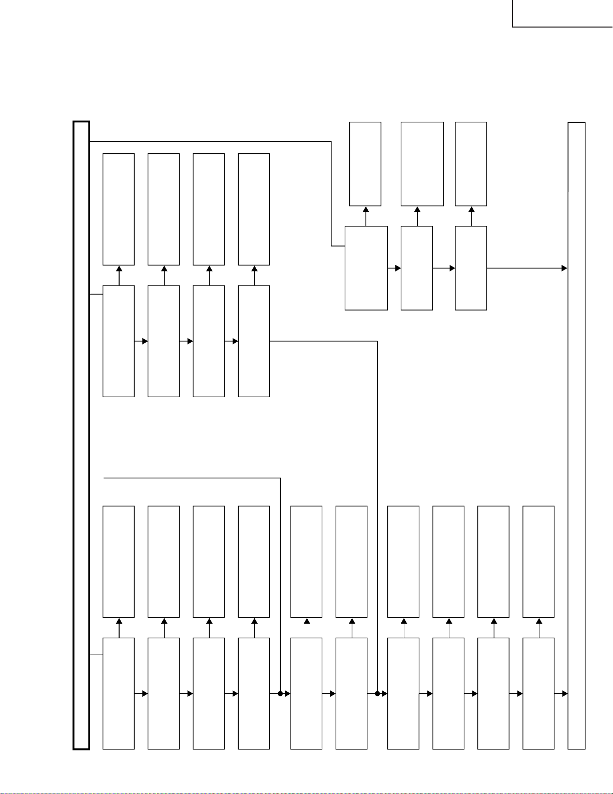
NO
YES
Is HD1/VD1 outputted to pins (9)
and (4) of IC801 (MAIN VIDEO
CHROMA), respectively?
Check IC801 and its peripheral
circuits.
NO
YES
Is HD2/VD2 outputted to
pins (9) and (4) of IC802
(SUB VIDEO CHROMA),
respectively?
Check IC802 and its
peripheral circuits.
NO
YES
Is HD1/VD1 outputted to pins
(28) and (27) of IC1901 (PLD),
respectively?
Check the circuit between pins
(9)/(4) of IC801 and pins
(27)/(28) of IC1901.
NO
YES
Is HD2/VD2 inputted to pins
(41) and (42) of IC1901
(PLD), respectively?
Check the circuit
between pins (9)/(4) of
IC802 and pins
(41)/(42) of IC1901.
NO
YES
Check IC1901 and its
peripheral circuits.
NO
YES
Is HDS/VDS inputted to pins
(39) and (40) of IC1901
(PLD), respectively?
Check IC1901 and its
peripheral circuits.
NO
YES
Is HD3/VD3 inputted to pins
(14) and (13) of IC604 (Sync.
Sep), respectively?
Check the circuit between pins
(7)/(6) of IC1901 and pins
(14)/(13) of IC604.
NO
YES
Is SP-HD/SP-VD/SP-CP
outputted to pins (16) , (28) and
(15) of IC604, respectively?
Check IC604 and its peripheral
circuits.
NO
YES
Is SP-HD/SP-VD/SP-CP
inputted to pins (5) , (3) and (8)
of IC1901, respectively?
Check the circuit between pins
(16)/(28)/(15) of IC604 and pins
(5)/(3)/(8) of IC1901.
NO
YES
Is PL-HD/PL-VD/PL-CP/PL-BLK
outputted to pins (30), (29), (31)
and (32) of IC1901, respectively?
Check IC1901 and its
peripheral circuits.
NO
YES
Is Hsync/Vsync/SCP inputted to
pins (1) , (2) and (31) of IC803
(RGB DECODER), respectively?
Check the circuit between pins
(30)/(29)/(31)/(32) of IC1901
and pins (1)/(2)/(31) of IC803.
NO
YES
Is HDM/VDM outputted to pins
(5) and (7) of IC807,
respectively?
Check IC807 and its peripheral
circuits.
YES
NO
Is HS/VS outputted to pins
(29) and (28) of IC803,
respectively?
Check IC803 and its peripheral
circuits.
Check PC I/F Unit.
Is HD3/VD3 outputted to pins
(7) and (6) of IC1901 (PLD),
respectively?
NO
YES
Is HD_50/VD_50 outputted to
pins (79) and (80) of IC803,
respectively?
Check IC803 and its peripheral
circuits.
NO
YES
Is HD_50/VD_50 inputted to
pins (3) and (4) of IC604,
respectively?
Check the circuit between pins
(79)/(80) of IC803 and pins
(3)/(4) of IC604.
NO
YES
YES
Check IC604 and its
peripheral circuits.
NO
Is SP-HD/SP-VD outputted to
pins (5) and (3) of IC1901,
respectively?
Check the circuit between pins
(16)/(28) of IC604 and pins
(5)/(3) of IC1901.
Is SP-HD/SP-VD outputted to
pins (16) and (28) of IC604,
respectively?
<MAIN system; 15k> <MAIN system; 1080i/625P>
<SUB system>
<MAIN system; D2/D3/D4>
Synchronization failure
•AVC System
LC-30HV4M
LC-30HV4H
61
Page 62

LC-30HV4M
LCD LED: ON
AVC-C LED: OFF
Check power switch, AC power cable and power unit of AVC-C.
LCD LED: OFF
AVC-C LED: ON
Check power switch, AC power cable and power unit of LCD.
LCD LED: BLINKING
(Once per second)
Check system cable, power switch, AC power cable and power unit of AVC-C.
LCD LED: BLINKING
(4 times per second)
Check cooling fan, IC2102 and peripheral circuits.
LCD LED: ON IN RED
AVC-C LED: ON IN RED
LCD LED never turns to
green.
Check power switch, AC power cable and power unit of LCD.
AVC-C LED never turns
to green.
Check power switch, AC power cable and power unit of AVC-C.
LCD panel backlight
never lights up.
Reset the lamp error count. (See adjustment procedure.)
Check Q6551, Q6554, Q6557, Q6560, Q6563, and Q6566 as well as peripheral circuits.
Initialize EEPROM. (See
adjustment procedure.)
If not successful: Check power switch, AC power cable and power unit of LCD.
No Power
LC-30HV4H
TROUBLE SHOOTING TABLE
(Display)
62
Page 63

TROUBLE SHOOTING TABLE (Continued)
No 800-MHz signal input at pins (186), (187), (191), (192), (196) and (197) of IC2201.
Check system cable and connector.
No signal output from pins (95), (96) and (97) of IC2201.
Check IC2201 and peripheral circuits.
Disconnect system cable and operate LCD independently. (Blue screen appears.)
Check system cable, connector and peripheral circuits.
Is each pin normal at IC4701?
Faulty: Check IC4701 and peripheral circuits.
Is each pin normal at IC4901?
Faulty: Check IC4901 and peripheral circuits.
Is each pin normal at IC4551?
Faulty: Check IC4551 and peripheral circuits.
Check SC4501, -4502, -4503 and -4504 and their cables.
Check outputs of main unit and headphone.
Is signal waveform normal at Q2105 and Q2106?
Faulty: Check Q2105 and Q2106 and peripheral circuits.
Is signal waveform normal at IC3802 and IC3804?
Faulty: Check IC3802 and IC3804 and peripheral circuits.
Is signal waveform normal at IC3805, IC3806 and IC3807?
Faulty: Check IC3805, IC3806 and IC3807 and peripheral circuits.
Check IC3809 and peripheral circuits.
1No Picture
2No Sound
(Display)
LC-30HV4M
LC-30HV4H
63
Page 64

LC-30HV4M
LC-30HV4H
CHASSIS LAYOUT (AVC System)
H
G
F
E
D
C
B
A
87109654321
64
Page 65

LC-30HV4M
LC-30HV4H
65
1716 1918151413121110
Page 66

LC-30HV4M
LC-30HV4H
CHASSIS LAYOUT (Display)
H
G
F
E
D
C
B
A
87109654321
66
Page 67

LC-30HV4M
LC-30HV4H
67
1716 1918151413121110
Page 68

LC-30HV4M
LC-30HV4H
SYSTEM BLOCK DIAGRAM (AVC System)
H
G
F
E
D
C
B
A
87109654321
68
Page 69

LC-30HV4M
LC-30HV4H
69
1716 1918151413121110
Page 70

LC-30HV4M
LC-30HV4H
SIGNAL FLOW BLOCK DIAGRAM (AVC System)
H
G
F
E
D
C
B
A
87109654321
70
Page 71

LC-30HV4M
LC-30HV4H
71
1716 1918151413121110
Page 72

LC-30HV4M
LC-30HV4H
POWER SYSTEM BLOCK DIAGRAM (AVC System)
H
G
F
E
D
C
B
A
87109654321
72
Page 73

LC-30HV4M
LC-30HV4H
73
1716 1918151413121110
Page 74

LC-30HV4M
LC-30HV4H
PC I/F UNIT BLOCK DIAGRAM (AVC System)
H
G
F
E
D
C
B
A
87109654321
74
Page 75

LC-30HV4M
LC-30HV4H
75
1716 1918151413121110
Page 76

LC-30HV4M
C
2
O
P
2
P
LC-30HV4H
SIGNAL BLOCK DIAGRAM (Display)
MAIN UNIT
H
IC2202
HDCP(KEY)
EEPROM
KEY IIC
TMDS
G
F
E
D
SC2201
DISPLAY
INPUT 1
SC2202
DISPLAY
INPUT 2
DDC IIC
DDC 5V
CONTROL
KEY
IC2201
TMDS
RECEIVER
IC2204
DDC
EEP-ROM
IC 2002
RESET
IC2001
MICRO
PROCESSOR
R/C RECEIVER
OPC, LED
QO23-0, QE23-0
HSYNC, VSYNC, CLO
CONFIG IIC
IC
C
EE
Q2004, Q2005
LEVEL
CONVERTER
IC
EE
C
B
A
AUDIO UNIT
J201
SPEAKER(L)
PLUG
OPERATION UNIT
SRS/FOCUS
AUDIO PROCESSOR
SOUND CONTROL
SOUND-AMP
76
IC3802
IC3804
IC3809
R/C,LED UNIT
IC3803
EXTENSION
DAC
J202
SPEAKER(R)
PLUG
87109654321
Page 77
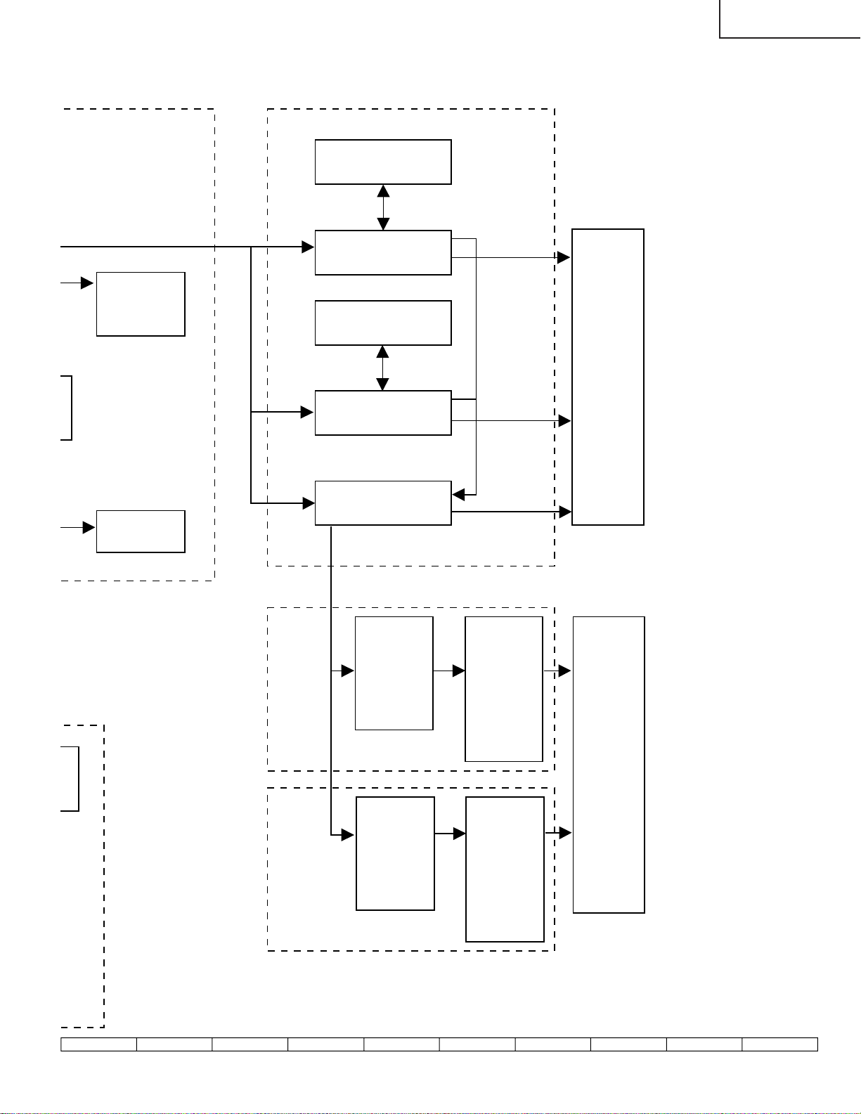
QE23-0
VSYNC, CLOCK
IC2203
CONFIG
EEPROM
LC-30HV4M
LC-30HV4H
LCD CONTROL(DIGITAL) UNIT
IC4902
FIFO MEMORY
IC4901
OSD DRIVE(ODD)
IC4702
FIFO MEMORY
LCD
PANEL
IC4701
OSD DRIVE(EVEN)
IC4551
IC2003
EEPROM
INVERTER-1 UNIT
N
INVERTER-2 UNIT
LCD CONTROL
OFL
Q6551
Q6554
Q6557
DC/AC
INVERTER
DRIVE
Q6560
Q6563
Q6566
DC/AC
INVERTER
DRIVE
T6551
T6552
T6553
T6554
T6555
T6556
DC/AC
TRANS
T6557
T6558
T6559
T6560
T6561
T6562
DC/AC
TRANS
BACK
LIGHT
77
1716 1918151413121110
Page 78

LC-30HV4M
G
G
1
R
-
V
LC-30HV4H
POWER UNIT BLOCK DIAGRAM (Displa y)
H
G
F
E
OPERATION
SW136
AC SW
P131
AA
INVERTER GND
+5V
LCD CONTROL(DIGITAL)
IC4112
3.3V REG
VSH+3.3V
FAN
IC4556
5V REG
DAC+5V
MAIN
(TMDS/MICOM)
P2103
MB
IC4559
IC4560
13V REG
VLS+13V
+8V
FAN VCC
IC2102
8V REG
P6907
MD
D
C
B
AUDIO
IC3801
9V REG
+9V
IC3811
5V REG
+13V
P3801
SA
+5V
P2106
MD
+5V
P2104
SA
P2003
RM
+2.5V
+3.3V
+5V STB
IC2105
2.5V RE
IC2104
3.3V RE
IC2
5V
A
R/C.LED
+5V STB
P101
RM
87109654321
78
Page 79

LC-30HV4M
LC-30HV4H
559
560
REG
+13V
IC2102
8V REG
IC4558
-6V REG
VEE-6V
IC4557
6V REG
IC4555
34V REG
VGH+34V
POWER
P4101
PC
PC
(CN5)
+13V
IC4516
3.3V REG
IC4515
2.5V REG
13V IC13V PANEL
B+3.3V CONT
B+2.5V CONT
INVERTER1
IC2105
2.5V REG
IC2104
3.3V REG
IC2101
5V REG
+13V
P2102
PB
P2101
PA
STB+6V
PB
(CN4)
PA
(CN3)
AA
(CN2)
+10V
+13V
STB+6V
CN1
AC IN
INV.VCC
P6557
PG
PE
(CN7)
INVERTER2
P6564
PH
INV.VCC
79
1716 1918151413121110
Page 80

LC-30HV4M
LC-30HV4H
OVERALL WIRING DIAGRAM-1/2 (AVC system)
H
G
F
E
D
C
B
A
87109654321
80
Page 81
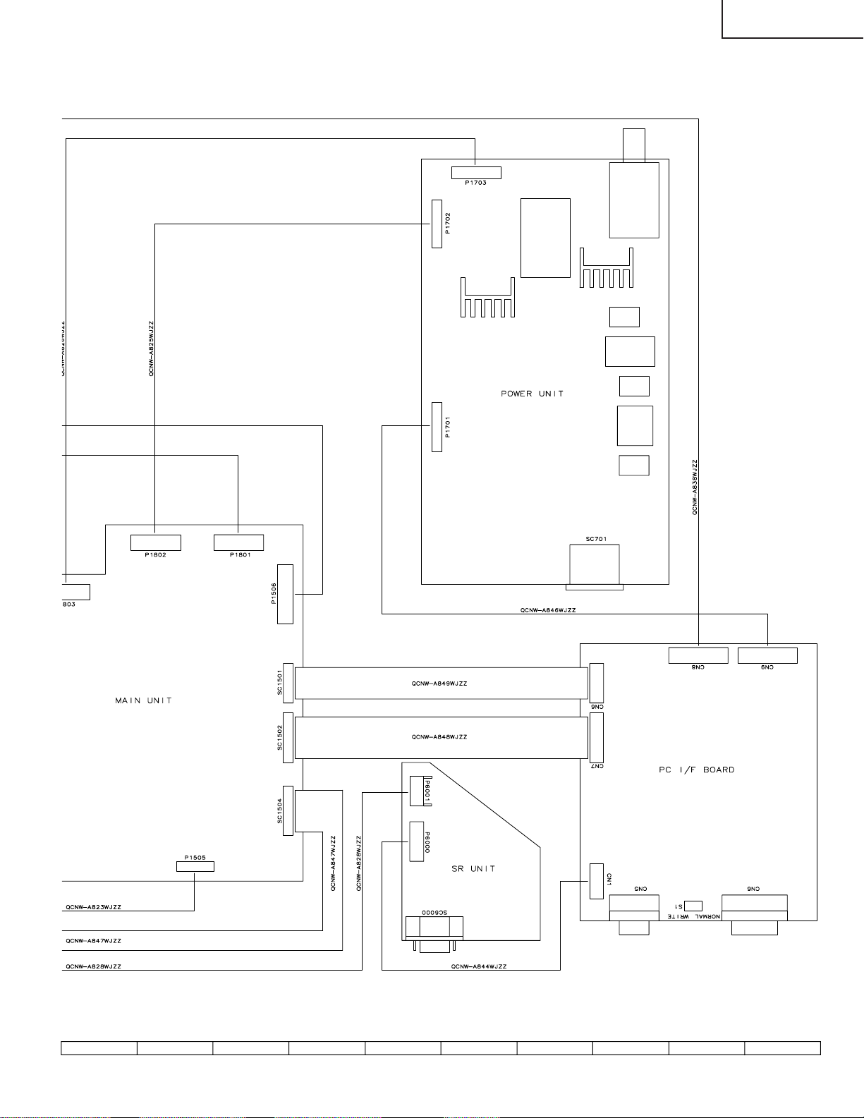
LC-30HV4M
LC-30HV4H
81
1716 1918151413121110
Page 82

LC-30HV4M
LC-30HV4H
OVERALL WIRING DIAGRAM-2/2 (AVC system)
H
G
F
E
D
C
B
A
87109654321
82
Page 83

LC-30HV4M
LC-30HV4H
83
1716 1918151413121110
Page 84

LC-30HV4M
LC-30HV4H
OVERALL WIRING DIAGRAM (Display)
H
G
F
E
D
C
B
A
87109654321
84
Page 85

LC-30HV4M
LC-30HV4H
85
1716 1918151413121110
Page 86

LC-30HV4M
LC-30HV4H
DESCRIPTION OF SCHEMATIC DIAGRAM
VOLTAGE MEASUREMENT CONDITION:
1. When the exclusive-use AC adapter is used, the colour
bar signal of colour bar generator for service is input to
get the normal screen. When the audio is minimized,
the voltage value is measured with the 20 kΩ/V tester.
INDICATION OF RESISTOR & CAPACITOR:
RESISTOR
1. The unit of resistance “Ω” is omitted.
(K=kΩ=1000 Ω, M=MΩ).
2. All resistors are ± 5%, unless otherwise noted.
(J= ± 5%, F= ± 1%, D= ± 0.5%)
3. All resistors are Carbon type, unless otherwise noted.
C : Solid W : Cement
S : Oxide Film T : Special
N : Metal Coating
CAPACITOR
1. All capacitors are mF, unless otherwise noted.
(P=pF=mmF).
2. All capacitors are Ceramic type, unless otherwise
noted.
(ML) : Mylar (T A) : Tantalum
(PF) : Polypro Film (ST) : Styrol
CAUTION:
This circuit diagram is original one, therefore there may be a
slight difference from yours.
IMPORTANT SAFETY NOTICE:
PARTS MARKED WITH
IMPORTANT FOR MAINTAINING THE SAFETY OF
THE SET. BE SURE TO REPLACE THESE PARTS
WITH SPECIFIED ONES FOR MAINTAINING THE
SAFETY AND PERFORMANCE OF THE SET.
“å”
( )ARE
86
Page 87

ËË
Ë SR Unit (AVC System)
ËË
H
G
F
LC-30HV4M
LC-30HV4H
E
D
C
B
A
654321
87
Page 88

LC-30HV4M
LC-30HV4H
Ë MAIN Unit-1/7 (AVC System)
H
G
F
E
D
C
B
A
87109654321
88
Page 89

LC-30HV4M
LC-30HV4H
89
1716 1918151413121110
Page 90

LC-30HV4M
LC-30HV4H
ËË
Ë MAIN Unit-2/7 (AVC System)
ËË
H
G
F
E
D
C
B
A
87109654321
90
Page 91

LC-30HV4M
LC-30HV4H
91
1716 1918151413121110
Page 92

LC-30HV4M
LC-30HV4H
ËË
Ë MAIN Unit-3/7 (AVC System)
ËË
H
G
F
E
D
C
B
A
87109654321
92
Page 93

LC-30HV4M
LC-30HV4H
93
1716 1918151413121110
Page 94

LC-30HV4M
LC-30HV4H
Ë MAIN Unit-4/7 (AVC System)
H
G
F
E
D
C
B
A
87109654321
94
Page 95

LC-30HV4M
LC-30HV4H
95
1716 1918151413121110
Page 96

LC-30HV4M
LC-30HV4H
Ë MAIN Unit-5/7 (AVC System)
H
G
F
E
D
C
B
A
87109654321
96
Page 97

LC-30HV4M
LC-30HV4H
97
1716 1918151413121110
Page 98

LC-30HV4M
LC-30HV4H
ËË
Ë MAIN Unit-6/7 (AVC System)
ËË
H
G
F
E
D
C
B
A
87109654321
98
Page 99

LC-30HV4M
LC-30HV4H
99
1716 1918151413121110
Page 100

LC-30HV4M
LC-30HV4H
ËË
Ë MAIN Unit-7/7 (AVC System)
ËË
H
G
F
E
D
C
B
A
87109654321
100
 Loading...