

Page 1
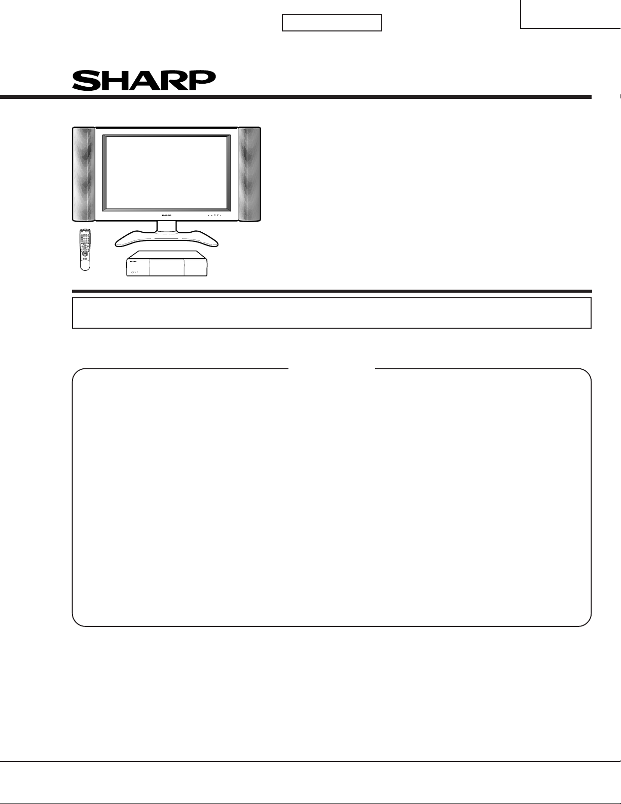
1st Edition
LC-30HV4E
SERVICE MANUAL
LCD COLOUR TELEVISION
MODEL
In the interests of user-safety (Required by safety regulations in some countries) the set should be restored
to its original condition and only parts identical to those specified should be used.
LC-30HV4E
CONTENTS
Page
» IMPORTANT SERVICE SAFETY PRECAUTION .....2
» SPECIFICATIONS................................................3
» OPERATION MANUAL ........................................ 4
» DIMENSIONS ....................................................10
» REMOVING OF MAJOR PARTS........................12
»
ADJUSTMENT PROCEDURES (AVC System) ..
» UPGRADING INSTALLED PROGRAMS ...........26
» ADJUSTMENT PROCEDURES (Display) .........29
» MAJOR IC INFORMATIONS..............................33
» TROUBLE SHOOTING TABLE ..........................52
» CHASSIS LAYOUT.............................................62
» SYSTEM BLOCK DIAGRAM (AVC System) ...... 66
» SIGNAL FLOW BLOCK DIAGRAM
(AVC System).....................................................68
19
» POWER SYSTEM BLOCK DIAGRAM
(AVC System).....................................................70
» PC I/F BLOCK DIAGRAM (AVC System) ..........72
» SIGNAL BLOCK DIAGRAM (Display)................ 74
» POWER UNIT BLOCK DIAGRAM (Display) ...... 76
» OVERALL WIRING DIAGRAM (AVC System) ... 78
» OVERALL WIRING DIAGRAM (Display)............ 82
» DESCRIPTION OF SCHEMATIC DIAGRAM ..... 84
» WAVEFORMS .................................................... 85
» SCHEMATIC DIAGRAM..................................... 86
» PRINTED WIRING BOARD ASSEMBLIES...... 159
» PARTS LIST .....................................................204
» PACKING OF THE SET ...................................246
Page
SHARP CORPORATION
Page 2
LC-30HV4E
2
2
IMPORTANT SERVICE SAFETY PRECAUTION
Ë
Service work should be perfomed only by qualified ser vice technicians who are thoroughly familiar with all safety checks and the servicing guidelines which follow:
WARNING
» Use an AC voltmeter having with 5000 ohm per volt,
or higher, sensitivity or measure the A C voltage drop
1. For continued safety, no modification of any circuit
should be attempted.
2. Disconnect AC power before servicing.
across the resisor.
» Connect the resistor connection to all exposed metal
parts having a return to the chassis (antenna, metal
cabinet, screw heads, knobs and control shafts,
CAUTION: FOR CONTINUED PROTECTION
AGAINST A RISK OF FIRE REPLACE ONLY WITH
SAME TYPE FUSE.
AVC SIDE: F701 (T2A, 250V), F702 (T2A, 250V),
F1702 (T4AL, 250V) FUSE.
LCD SIDE: F1(T3.15AL, 250V), F6551, F6552, F6553,
F6554, F6555, F6556 (T2.5AL, 250V)
escutcheon, etc.) and measure the AC voltage drop
across the resistor.
All checks must be repeated with the AC cord plug
connection reversed. (If necessar y, a nonpolarized
adaptor plug must be used only for the purpose of
completing these checks.)
Any reading of 35V peak (this corresponds to 0.7
milliamp. peak AC.) or more is excessive and
BEFORE RETURNING THE RECEIVER
(Fire & Shock Hazard)
indicates a potential shock hazard which must be
corrected before returning the monitor to the owner .
Before returning the receiver to the user, perform
the following safety checks:
1. Inspect all lead dress to make certain that leads are
not pinched, and check that hardware is not lodged
between the chassis and other metal parts in the
receiver.
2. Inspect all protective devices such as non-metallic
DVM
AC SCALE
control knobs, insulation materials, cabinet backs,
adjustment and compartment covers or shields,
isolation resistor-capacitor networks, mechanical
50k ohm
10W
insulators, etc.
3. To be sure that no shock hazard exists, check for
leakage current in the following manner.
» Plug the AC cord directly into a 110~240 volt A C outlet,
and connect the DC power cable into the receiver's
0.15 µF
TEST PROBE
DC jack. (Do not use an isolation transformer for this
test).
» Using two clip leads, connect a 1.5k ohm, 10 watt
resistor paralleled by a 0.15µF capacitor in series
with all exposed metal cabinet parts and a known
earth ground, such as electrical conduit or electrical
TO EXPOSED
METAL PARTS
CONNECT TO
KNOWN EARTH
GROUND
ground connected to an earth ground.
234567890123456789012345678901212345678901234567890123456789012123456789012345678901234567890121
SAFETY NOTICE
Many electrical and mechanical parts in Plasma Display
television have special safety-related characteristics.
These characteristics are often not evident from visual
inspection, nor can protection afforded by them be
necessarily increased by using replacement components
rated for higher voltage , w attage , etc.
Replacement parts which have these special safety
characteristics are identified in this manual; electrical
and shaded areas in the
Schematic Diagrams.
For continued protection, replacement parts must be
identical to those used in the original circuit.
The use of a substitute replacement parts which do not
have the same safety characteristics as the factory
recommended replacement parts shown in this service
manual, may create shock, fire or other hazards.
components having such features are identified by “ å”
234567890123456789012345678901212345678901234567890123456789012123456789012345678901234567890121
2
Replacement Parts List
and
Page 3
SPECIFICATIONS
Item 30" LCD COLOUR TV, Model:LC-30HV4E
Video Colour System PAL/SECAM/NTSC 3.58/NTSC 4.43/PAL 60
TV
Function
B/G, D/K, I, L/L’
VHF/UHF
E2–E69ch, F2–F10ch, I21–I69ch, IR A–IR Jch
CATV
Hyper-band, S1–S41ch
TV-Tuning System
Auto Preset 99 ch, Auto Label, Auto Sort
STEREO/BILINGAL NICAM/IGR
Terminals SCART (AV in, RGB in, TV out)
INPUT 2
SCART (AV in/out, S-VIDEO in, AV Link)
INPUT 3
SCART (AV in/out, S-VIDEO in, RGB in), Component
ANTENNA 75 Ω Din Type
INPUT 4 S-VIDEO, AV in
PC
15 Pin mini D-Sub, Audio in (Ø 3.5mm jack)
OSD language
English/German/French/Italian/Spanish/Dutch/Swedish/Portuguese/Greek/
Finnish/Russian/Turkish
Power Requirement
AC 220–240 V, 50/60 Hz
Power
Consumption
32 W (0.7 W Standby)
Weight
5.4 kg (w/o stand), 5.5 kg (with stand)
Accessories
Operation manual, Remote control unit (× 1), System cable ( × 1), AC cord
(× 2), LR6 (“AA” size) Alkaline battery (× 2), Stand unit (× 1), Cable clamp
(× 1)
TV-standard (CCIR)
Receiving
Channel
Rear INPUT 1
Front
LCD panel 30" Advanced Super View & BLACK TFT LCD
Number of dots 2,949,120 dots (1280 × 768 × 3 dots)
Brightness 430 cd/m
2
Backlight 60,000 hours (at Save1)
Viewing angles H : 170° V : 170°
Audio amplifier 10W × 2
Speakers Ø 8 cm 2pcs
AVC
System
AV OUTPUT Audio (Variable, Fixed), S-VIDEO out, AV out
Headphones
Ø 3.5mm jack
AVC System
Display
AVC System
Display
109 W (0.9 W Standby) (Method IEC60107)
15.7 kg (w/o stand), 19.5 kg (with stand)
DC OUTPUT DC6.5V 7W MAX
LC-30HV4E
3
Page 4
LC-30HV4E
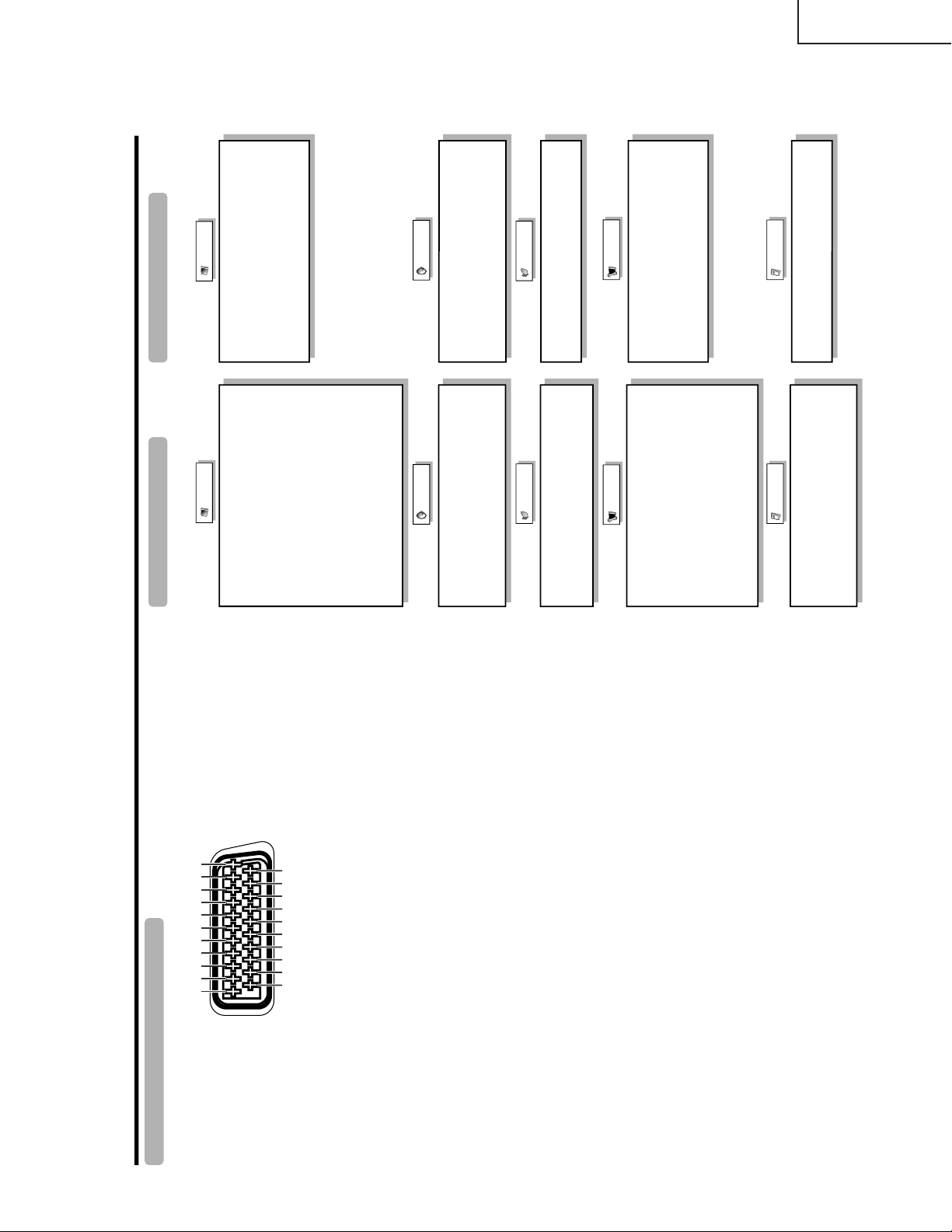
Part names
OPC indicator*
STANDBY/ON indicator
MAIN POWER
button
OPC sensor
Remote control sensor
indicator
Display
STANDBY/ON button
(
)
INPUT
button
VOLUME buttons
(
/
)
CHANNEL buttons
(CH
/
)
Remote control sensor
*OPC: Optical Picture Control
(See Pages 36 and 38.)
INPUT 1 terminal
(SCART)
INPUT 3 terminals (Y, P
B
(C
B
)
,
P
R
(C
R
))
INPUT 2 terminal (SCART)
AV OUTPUT terminal
(S-VIDEO)
DISPLAY OUTPUT1 terminal
AC INPUT terminal
CLEAR*
POWER button
RS-232C terminal
INPUT 4 terminal (S-VIDEO)
PC INPUT terminal (AUDIO)
INPUT 4 terminals (AUDIO)
INPUT 3 terminal (SCART)
AV OUTPUT terminal
(VIDEO)
AV OUTPUT terminals
(AUDIO)
PC INPUT terminal
(ANALOG RGB)
* If the AVC System is switched on but it does not appear to be operating corr ectly, it may need resetting. In this
case, press CLEAR, shown in the diagram, lightly with the end of a ballpoint pen or other pointed object.
This will reset the System as shown below.
• AV MODE resets to STANDARD.
• TV channel resets to channel 1.
• Dual screen resets to normal.
• Audio setting initialises.
• SRS resets to OFF.
• Image position is initialised.
NOTE
• Pressing CLEAR will not work if the System is in standby mode (indicator lights red).
• Pressing CLEAR will not delete channel preset or password. See page 60 for clearing the password when you know it.
See page for initialising to the factor y preset values when you forget your password.
ANTENNA INPUT terminal
AVC System
STANDBY/ON indicator
DISPLAY OUTPUT2
terminal
INPUT 4 terminal (VIDEO)
(How to open the door)
Front view
Rear view
Headphone
DC OUTPUT terminal
(Terminal for expanded
functionality in the near
future.)
(When connecting headphones,
the sound from the speakers is
muted.)
OPERATION MANUAL
4
Page 5
LC-30HV4E
Part namesPart names
1
(STANDBY/ON)
To switch the power on and off.
2
(FREEZE/HOLD for TELETEXT)
TV/External input mode: Change the still image mode.
TELETEXT mode: Freeze a multi-page on screen while other
pages are automatically updated. Press
again to return to the
normal image.
3
(DUAL screen)
Set the dual picture mode. Press
again to return to normal view.
(See page 61.)
4
(WIDE MODE/ T/B/F)
TV/External input mode: Change the wide image mode.
TELETEXT mode: Set the area of magnification. (full/upper half/
lower half)
5 AV MODE
Select a video setting: AV MODE (STANDARD, DYNAMIC, MOVIE,
GAME, USER), PC MODE (STANDARD, USER) (See page 51.)
6 SOUND
Select the sound multiplex mode.
7
(SRS and FOCUS)*
Select SRS and FOCUS sound system.
8
(Flashback)
Press to return to the previous channel in normal viewing mode.
Press to return to the previous page in TELETEXT mode.
9
/
(VOLUME)
Set the volume.
10
(Reveal hidden for TELETEXT)
TELETEXT mode: Display hidden characters.
11
(SUBPAGE for TELETEXT)
TELETEXT mode: Change the picture mode for sub-page selecting.
12 MENU
Display the MENU screen.
13
(CHANNEL INFORMATION)
Display the channel information and time.
14
(INPUT SOURCE)
Select an input source. (TV, INPUT 1, INPUT 2, INPUT 3, INPUT 4,
PC)
15 SLEEP
Set the Sleep timer.
16
(MUTE)
Mute the sound.
17 0 – 9
TV/External input mode: Set the channel.
TELETEXT mode: Set the page.
18
(Digit for channel select)
Change the digits of the selected TV channel.
19 Colour (RED/GREEN/YELLOW/BLUE)
TELETEXT mode: Select a page.
20 CH
/CH
(
/
)
TV/External input mode: Select the channel.
TELETEXT mode: Set the page.
21
(TOP Overview for TELETEXT)
TELETEXT mode: Display an index page for CEEFAX/FLOF
information. TOP Overview for TOP programme.
22
(TELETEXT)
Select the TELETEXT mode. (all TV image, all TEXT image, TV/TEXT
image)
23 RETURN
MENU mode: Return to the previous menu screen.
24 ENTER
Execute a command.
Return to the initial image position after moving with
/
/
/
.
25
/
/
/
(Cursor)
Select a desired item on the setting screen.
Move the picture on the screen.
1
2
3
4
5
6
7
8
9
10
11
12
14
15
13
16
17
18
19
20
21
22
23
24
25
NOTE
• When using the r emote contr ol unit, point it
at the Display.
*
is a trademark of SRS Labs, Inc.
FOCUS technology is incorporated under
license from SRS Labs, Inc.
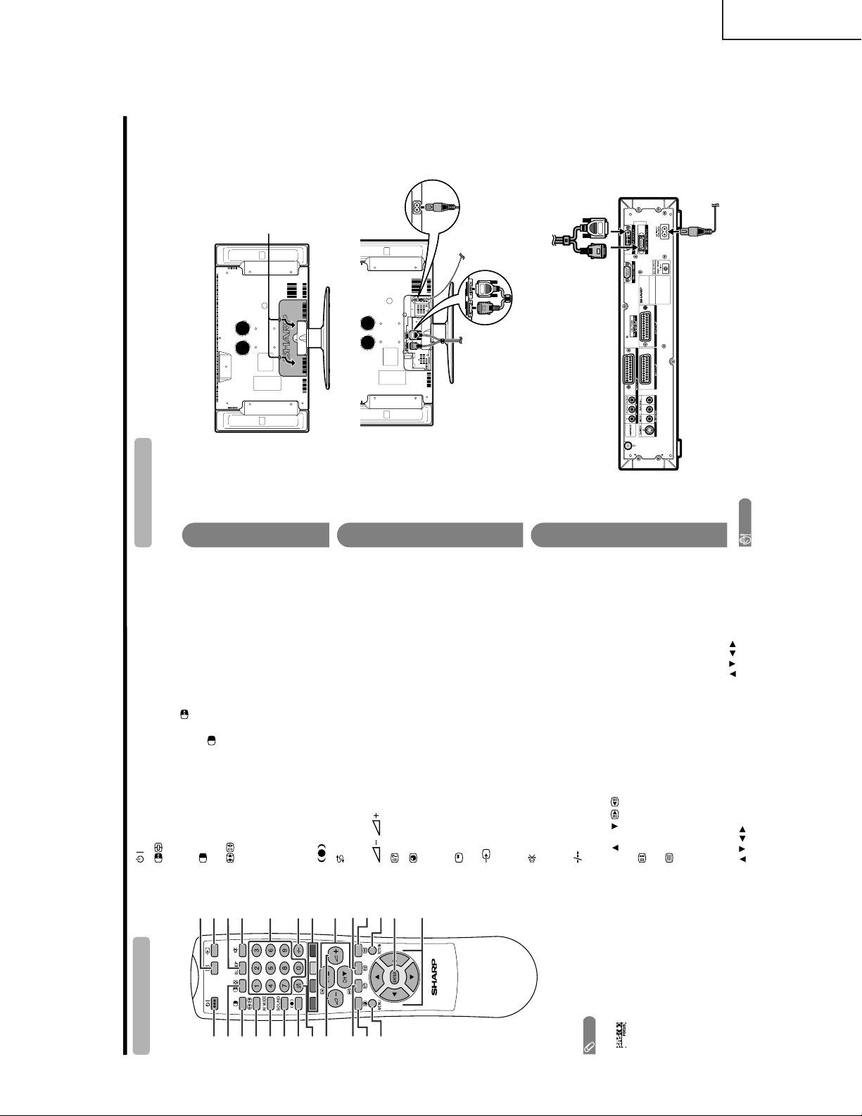
Remote control unit
AC INPUT
110V–240V
DISPLAY INPUT2 DISPLAY INPUT1
System cable
AVC System (rear view)
AC cord
Display (rear view)
AC cord
System cable
(GREY)
Connect the plug firmly
until the hooks on both
sides click.
(WHITE)
Connect the plug into the
terminal and secure it by
tightening the thumb screws.
(GREY) (WHITE)
Setting the System
After putting the Display and the AVC System in place, connect the system cables and AC cords. Use the
cable clamp for bundling the cables.
Press down the two
upper hooks to remove
the cover toward you.
Connecting the system cable and the AC cord to the Display
1
2
3
Removing the terminal cover
Connecting the system cable and the AC cord to the AVC System
CAUTION
• TO PREVENT RISK OF ELECTRIC SHOCK, DO NOT TOUCH UN-INSULATED PARTS OF ANY CABLES WITH THE
AC CORD CONNECTED.
5
Page 6
LC-30HV4E
Preparation
4
5
6
Attaching the clamp to the leg of the Display
Bundling the cables with the clamp
Closing the terminal cover
Display (rear view)
Cables come out from
the small opening.
Setting the Display on the wall
Setting the AVC System with the stand
CAUTION
• Installing the LCD Colour TV requires special skill that should only be performed by qualified service personnel.
Customers should not attempt to do the work themselves. SHARP bears no responsibility for improper mounting or
mounting that results in accident or injury.
1
Using an optional bracket to mount the Display
• You can ask a qualified service personnel about using an optional AN-37AG1 bracket to mount the Display
to the wall.
• Carefully read the instructions that come with the bracket before beginning work.
Vertical mounting Angular mounting
Hanging on the wall
AN-37AG1 wall mount bracket. (See the bracket instructions for details.)
How to install the AVC System vertically using the stand unit.
• Use the supplied stand unit for installing the AVC System vertically in an upright position.
Stick each spacer to the
stand as shown.
Peel each spacer
away from the
paper and attach
to the four bulging
areas on the stand.
2
Attach each cushion to
the stand as shown.
3
Fit the stand to the AVC
System.
Peel each cushion
away from the
paper and attach
to the four areas at
the bottom.
Insert the stand into the AVC
System, making sure that the
thick and thin bulges of the
stand align with the big and
small holes on the AVC
System.
Stand
spacer
Bulge
Stand cushion
Thin bulge
Thick
bulge
Big hole
Small
hole
4
Attach the stand using the
stand screws as shown.
Stand screw
The AVC System installed
vertically with the stand.
NOTE
• When mounting the AVC System vertically, always use the supplied stand. Be careful not to block vent holes when
standing up directly on the floor or a flat surface as this can result in equipment failure.
Attaching point
Attaching point
Bulge
6
Page 7
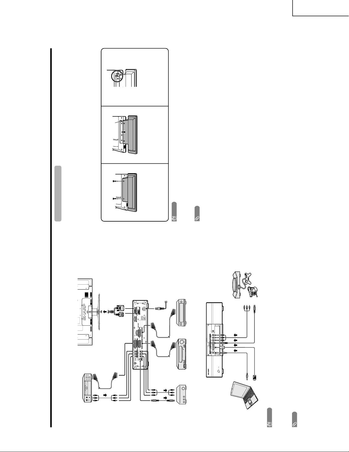
Using external equipment
Display
(rear view)
DVD player
AVC System
(rear view)
AVC System
(front view)
AV Receiver
(Built-in Tuner Amp)
VCR Decoder
Game console/CamcorderPC
You can connect many types of external equipment to your System, like a decoder, VCR, DVD player, PC, game
console and camcorder. To view external source images, select the input source from b on the remote
control unit or INPUT on the Display.
CAUTION
• To protect all equipment, always turn off the AVC System before connecting to a decoder, VCR, DVD player, PC, game
console, camcorder or other external equipment.
• The S-video signal only outputs when “INPUT2” or “INPUT3” is selected for “Y/C”, or when from the INPUT 4 terminal (S-
VIDEO). Only the S-video signal can output from the INPUT 4 terminal (S-VIDEO).
NOTE
• Please refer to the relevant operation manual (DVD player, PC, etc.) carefully before making connections.
Removing the speakers
This unit has detachable type speakers.
You can detach the system speakers when using external amplifier/speakers.
Before detaching (or attaching) speakers, unplug the AC cord from the AC outlet.
Before attaching/detaching speakers
• Before performing work make sure to turn off the System.
• Before performing work spread cushioning over a flat surface to lay the Display on. This will prevent it from
being damaged.
CAUTION
• The speaker terminals on the Display is only for the attached speakers. Do not connect any third party plug or speaker to
the terminal.
• Insert the speaker plug completely into the terminal.
• Do not handle or move the Display by the speakers.
NOTE
• Perform the same steps for both left and right speakers.
• To attach the speakers, perform the above steps in reverse order.
123
Unfasten the screws used to
secure the speakers in place.
Take hold of the speaker and
slowly slide it sideways.
(The speaker plug is still
inserted, so make sure not to
pull the speaker too far.)
Remove the speaker plug from
the terminal on the Display.
(Do not remove the plug by
pulling the cord.)
Now the speaker can be
detached from the Display.
Speaker
plug
LC-30HV4E
7
Page 8
LC-30HV4E
RS-232C port specifications
Return codeCommand 4-digits Parameter 4-digits
PC Control of the System
• When a program is set, the display can be controlled from the PC using the RS-232C terminal.
The input signal (PC/video) can be selected, the volume can be adjusted and various other adjustments and
settings can be made, enabling automatic programmed playing.
•
Attach an RS-232C cable cross-type (commercially available) to the supplied Din-D/sub RS-232C for the
connections.
NOTE
• This operation system should be used by a person who is accustomed to using PC.
Communication conditions
Set the RS-232C communications settings on the PC to match the display’s communications conditions. The
display's communications settings are as follows:
Baud rate:
Parity bit:
Data length:
Stop bit:
Flow control:
9,600 bps
8 bits
None
1 bit
None
Appendix
Command format
Communication procedure
Send the control commands from the PC via the RS-232C connector.
The Display operates according to the received command and sends a response message to the PC.
Do not send multiple commands at the same time. Wait until the PC receives the OK response before sending
the next command.
Eight ASCII codes e CR
Command 4-digits:Command. The text of four characters.
Parameter 4-digits:Parameter 0 – 9, x, blank, ?
Parameter
Input the parameter values, aligning left, and fill with blank(s) for the remainder. (Be sure that four values are input for the
parameter.)
When the input parameter is not within an adjustable range,
“ERR” r
eturns. (Refer to “Response code format”.)
No problem to input any numerical value for
“x” on the table.
When “?” is input for some commands, the present setting value responds.
C1 C2 C3 C4 P1 P2 P3 P4
0055
100
– 30
0009
0
????
?
Commands
P
I
I
I
I
I
I
I
I
I
I
I
I
I
A
A
A
A
A
A
V
H
H
V
V
C
P
POWER OFF (STANDBY)
INPUT SWITCHING (TOGGLE)
TV (CHANNEL FIXED)
TV (CHANNEL SELCTION) (1
– 99)
INPUT1 – 4 (1 – 4)
PC
INPUT1 (CVBS)
INPUT1 (RGB)
INPUT2 (CVBS)
INPUT2 (Y/C)
INPUT3 (CVBS)
INPUT3 (Y/C)
INPUT3 (RGB)
INPUT3 (COMPONENT)
TOGGLE
STANDARD
DYNAMIC
MOVIE
GAME
USER
VOLUME (0 – 60)
H-POSITION (AV) (10– 10)
H-POSITION (PC) (90– 90)
V-POSITION (AV) (30– 30)
V-POSITION (PC) (60– 60)
CLOCK ( 90 – 90)
PHASE ( 20 – 20)
POWER SETTING
INPUT SELECTION A
INPUT SELECTION B
AV MODE
SELECTION
VOLUME
POSITION
O
T
T
T
A
P
N
N
N
N
N
N
N
N
V
V
V
V
V
V
O
P
P
P
P
L
H
W
G
V
V
V
C
P
P
P
P
P
P
P
P
M
M
M
M
M
M
L
O
O
O
O
C
S
R
D
D
D
D
D
1
1
2
2
3
3
3
3
D
D
D
D
D
D
M
S
S
S
S
K
E
0
x
0
*
*
x
0
1
0
1
0
1
2
3
0
1
2
3
4
5
*
*
*
*
*
*
*
_
_
*
_
_
_
_
_
_
_
_
_
_
_
_
_
_
_
*
*
*
*
*
*
*
_
_
_
_
_
_
_
_
_
_
_
_
_
_
_
_
_
_
_
*
*
*
*
*
*
_
_
_
_
_
_
_
_
_
_
_
_
_
_
_
_
_
_
_
_
_
_
_
_
_
CONTROL ITEM COMMAND PARAMETER
CONTROL
CONTENTS
W
W
W
W
W
W
W
W
W
W
W
W
S
S
S
S
S
T
T
D
C
C
T
T
D
TOGGLE
NORMAL
FULL 14:9
ZOOM 14:9
PANORAMA
FULL
CINEMA 16:9
CINEMA 14:9
NORMAL
FULL
DOT BY DOT
CINEMA
TOGGLE
OFF
SRS
FOCUS
SRS FOCUS
DUAL SCREEN OFF
DUAL SCREEN ON
DIRECT CHANNEL (1
– 99)
CHANNEL UP
CHANNEL DOWN
TEXT OFF
TEXT ON (TOGGLE)
DIRECT PAGE JUMP (100
– 899)
WIDE MODE
SRS
DUAL SCREEN
CHANNEL
TEXT
I
I
I
I
I
I
I
I
I
I
I
I
R
R
R
R
R
W
W
C
H
H
E
E
C
D
D
D
D
D
D
D
D
D
D
D
D
S
S
S
S
S
I
I
C
U
D
X
X
P
E
E
E
E
E
E
E
E
E
E
E
E
S
S
S
S
S
N
N
H
P
W
T
T
G
0
1
2
3
4
5
6
7
8
9
1
1
0
1
2
3
4
0
1
*
x
x
0
1
*
_
_
_
_
_
_
_
_
_
_
0
1
_
_
_
_
_
_
_
*
_
_
*
_
_
_
_
_
_
_
_
_
_
_
_
_
_
_
_
_
_
_
_
_
_
*
_
_
_
_
_
_
_
_
_
_
_
_
_
_
_
_
_
_
_
_
_
_
_
CONTROL ITEM COMMAND PARAMETER
CONTROL
CONTENTS
NOTE
• If an underbar (_) appears in the parameter column, enter a space.
• If an asterisk (*) appears, enter a value in the range indicated in brackets under CONTROL CONTENTS.
Return code (0DH)
Response code format
Normal response
Problem response (communication error or incorrect command)
Return code (0DH)
OK
ERR
8
Page 9
LC-30HV4E
Appendix
SCART (INPUT 1)
1. Audio right output
(TV Monitor out)
2. Audio right input
3. Audio left output
(TV Monitor out)
4. Common earth for audio
5. Earth for blue
6. Audio left input
7. Blue input
8. Audio-video control
9. Earth for green
10. Not used
11. Green input
12. Not used
13. Earth for red
14. Not used
15. Red input
16. Red/Green/Blue control
17. Earth for video
18. Earth for Red/Green/Blue
control
19. Video output
(TV Monitor out)
20. Video input
21. Plug shield
SCART (INPUT 2)
1. Audio right output
2. Audio right input
3. Audio left output
4. Common earth for audio
5. Earth
6. Audio left input
7. Not used
8. Audio-video control
9. Earth
10. AV LINK control
11. Not used
12. Not used
13. Earth
14. Not used
15. Chroma S-Video input
16. Not used
17. Earth for video
18. Earth
19. TV Monitor output
20. Video input/S-video input
21. Plug shield
SCART (INPUT 3)
1. Audio right output
2. Audio right input
3. Audio left output
4. Common earth for audio
5. Earth
6. Audio left input
7. Blue input
8. Audio-video control
9. Earth
10. Not used
11. Green input
12. Not used
13. Earth
14. Not used
15. Red input/Chroma S-Video
input
16. Red/Green/Blue control
17. Earth for video
18. Earth
19. TV Monitor output
20. Video input/S-video input
21. Plug shield
1 3 5 7 9 111315171921
2 4 6 8 101214161820
Connecting pin assignments for SCART
Various audio and video devices may be connected via the SCART terminals.
Basic adjustment settings
AV input mode menu items
List of AV menu items to help you with
operations
Contrast
Brightness
Colour
Tint
Sharpness
Advanced
C.M.S.
Colour Temp
Black
Monochrome
Film Mode
I/P Setting
DNR
Picture
Power Save
No Signal off
No Operation off
Auto Installation
Programme Setup
Child Lock
Position
WSS
4:3 Mode
Full Mode
Rotate
Language
Treble
Bass
Balance
Surround.
Input Select
Audio Out
Cool Climate
Colour System
Audio
Power control
Setup
Option
PC input mode menu items
List of PC menu items to help you with
operations
Contrast
Brightness
Red
Green
Blue
C.M.S.
Picture
Power Save
Power Management
Input Signal
Auto Sync.
Fine Sync.
Rotate
Language
Audio
Power control
Setup
Option
Treble
Bass
Balance
Surround
Audio Out
Cool Climate
9
Page 10
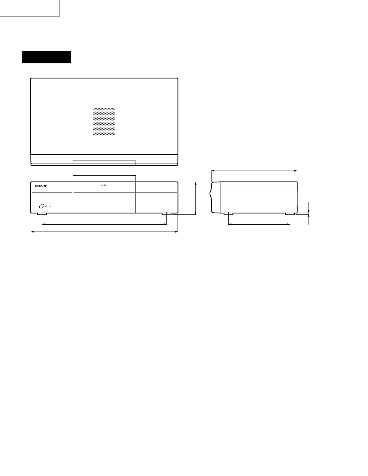
LC-30HV4E
DIMENSIONS
AVC System
183
365
430
Unit: mm
250
95
5
180
10
Page 11
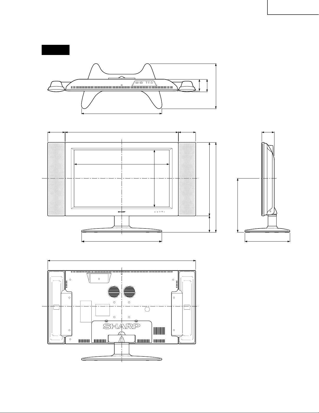
LC-30HV4E
545
545
305608
385
84.5
1002
305
84.5
364
766
117.5 117.5
643
497
111
79
Unit: mm
Display
11
Page 12
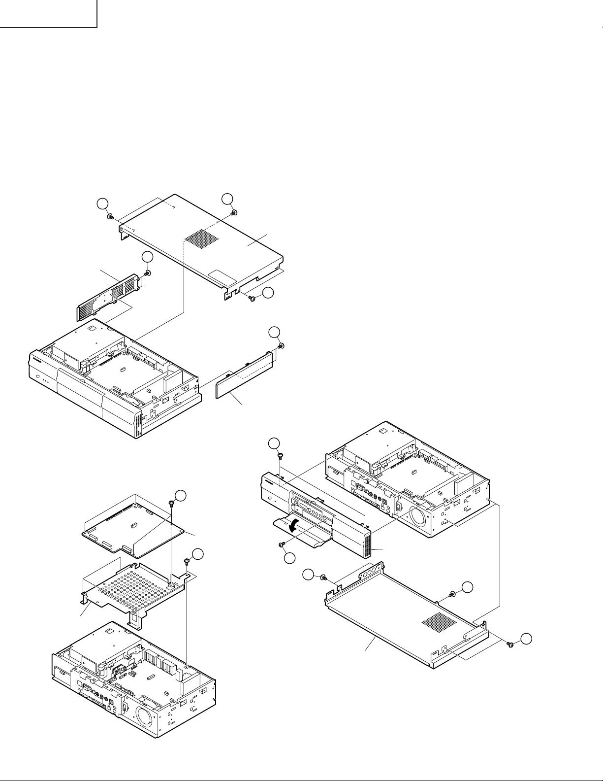
LC-30HV4E
REMOVING OF MAJOR PARTS
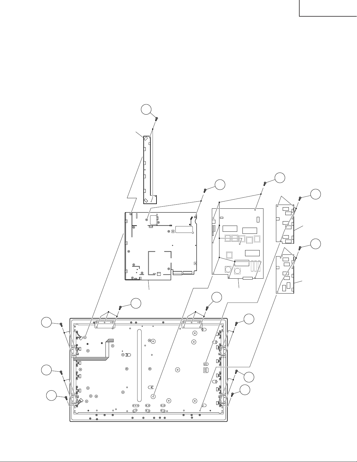
Ë Ë
Ë AVC System
Ë Ë
1. Remove the five top panel retaining screws and slide the top panel backward to remove it.
2. Remove the four side panel retaining screws on both the right and left sides and slide the side panels
backward to remove them.
3. Remove the three front panel retaining screws and remove the front panel.
4. Remove the five bottom panel retaining screws and slide the bottom panel backward to remove it.
5. Remove the four screws securing the main PWB angle and remove the angle upward.
6. Remove the four screws securing the main PWB to the angle and remove the main PWB.
1
Side panel, left
1
Top panel
2
1
2
Side panel, right
3
Main PWB angle
6
Main PWB
5
3
Front panel
4
4
4
Bottom panel
12
Page 13
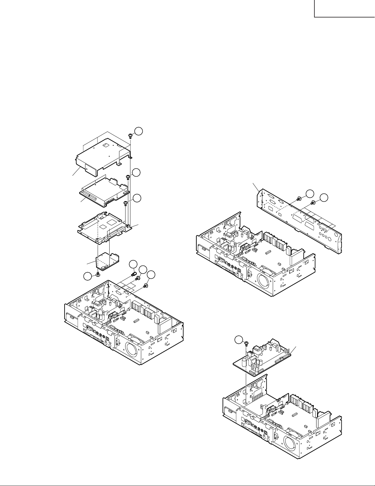
7. Remove the system/control terminal retaining:
Rear chassis
9-2
9-1
7-1. Remove the four hex head screws securing the terminals of the system and control cables (white).
7-2. Remove the two screws securing the terminal of the system cable (gray).
7-3. Remove the rear chassis retaining screw.
8. Remove the PC I/F and SR units:
8-1. Remove the four PC I/F unit shield retaining screws and remove the shield.
8-2. Remove the six PC I/F unit retaining screws and remove the I/F unit.
8-3. Remove the two PC I/F unit angle retaining screws and remove the angle.
8-4. Remove the two SR unit retaining screws and remove the SR unit.
9. Remove the rear chassis:
9-1. Remove the two tuner nuts and washers.
9-1. Remove the 13 rear chassis retaining screws and remove the rear chassis.
10. Remove the three power supply board retaining screws and remove the power supply board.
8-1
8-2
PC I/F unit shield
LC-30HV4E
PC I/F unit
SR unit
8-4
8-3
PC I/F unit angle
7-1
7-2
7-3
10
Power unit
13
Page 14
LC-30HV4E
11. Remove the AV unit:
11-1. Remove the five AV unit retaining screws and remove the AV unit.
11-2. Remove the three AV unit angle retaining screws and remove the angle.
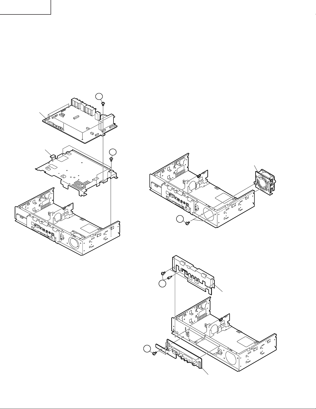
12. Remove the fan:
12-1. Remove the two cooling fan retaining screws and remove the cooling fan.
13. Remove unit from the front chassis:
13-1. Remove the two hex head screws and two screws securing the front shield to the front chassis and
remove the front shield.
13-2. Remove the four screws securing the front unit and remove the unit.
11-1
AV unit
AV unit angle
11-2
Cooling Fan
12-1
13-1
Front shield
13-2
14
Front unit
Page 15
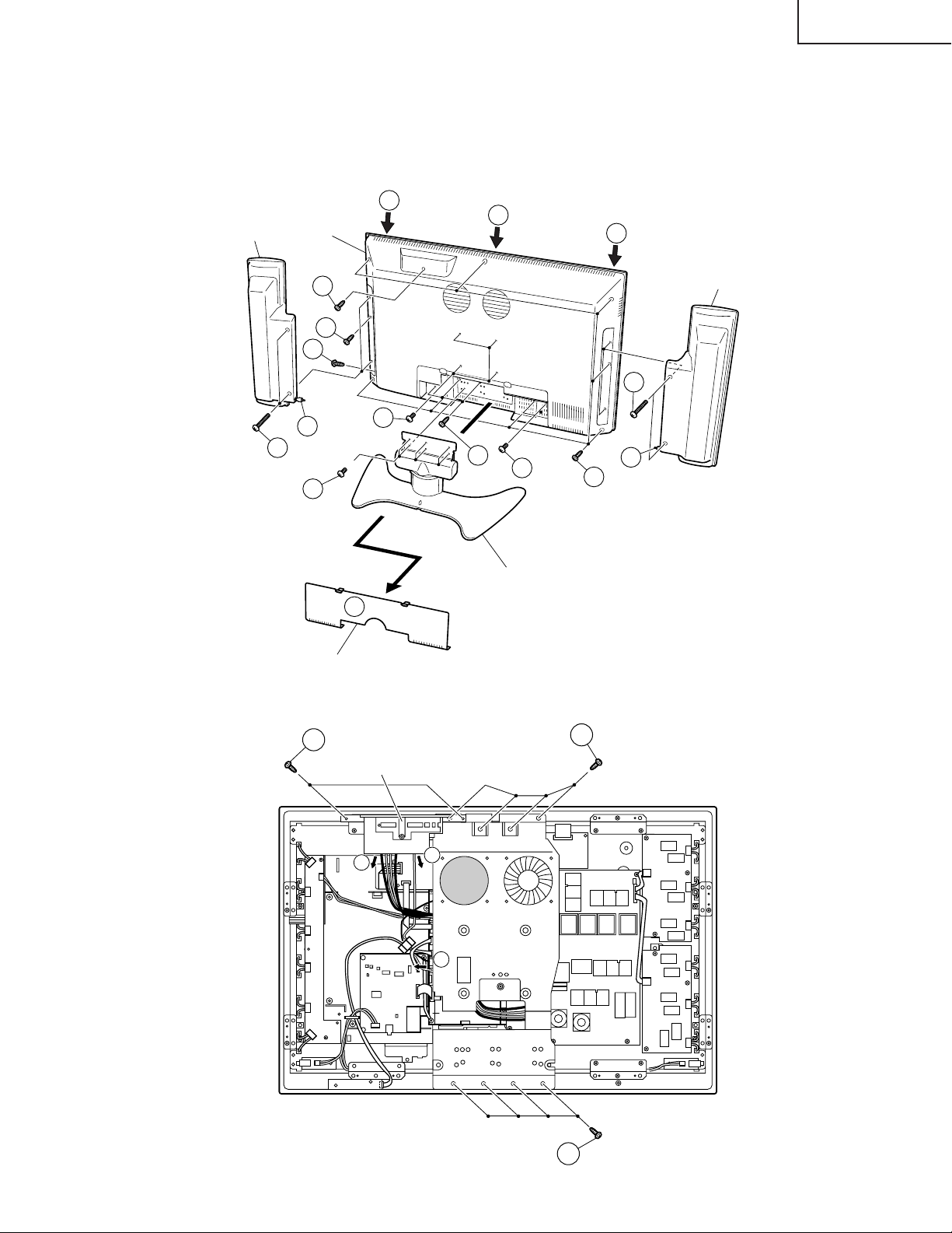
Ë Ë
Ë Display
Ë Ë
1. Take off bottom terminal cover.
2. Take off the speaker by removing 4 screws and disconnecting speaker terminals.
3. Take off the table stand by removing 6 screws.
4. Take off the rear cabinet by removing 18 screws and releasing the front cabinet's 6 hooks.
Speaker
4
Rear Cabinet
4
4
LC-30HV4E
Speaker
2
4
4
4
2
3
1
Terminal Cover
2
4
4
4
Table Stand
2
4
5. Take off the operation cover assembly by removing 2 screws and detaching the connector.
6. Take off the center angle by removing 8 screws and disconnecting 1 lead wire from the fan.
5
Operation Cover Ass'y
5
P131
P130
5
6
P2103
6
Center Angle
6
15
Page 16
LC-30HV4E
7. Take off the digital PWB by detaching 7 connectors and removing 4 screws.
8. Take off the LED PWB by detaching one connector and removing 2 screws.
9. Take off the speaker (L) PWB by detaching one connector and removing one screw.
10.Take off the speaker (R) PWB by detaching one connector and removing one screw.
9
Speaker(L)
PWB
P201
9
8
7
LED PWB
7
7
7
7
SC4502
7
SC4551
SC491
7
7
Digital
PWB
SC4503
7
13
Main
PWB
10
Speaker(R)
PWB
P202
10
8
11.Take off the main board by detaching 8 connectors and removing 4 screws.
12.Take off the SOUND PWB assembly by detaching 3 connectors and removing 4 screws.
13.Take off the 2 reinforcement angles by removing 3 screws from each angle.
14.Detach each connector.
Inverter 1PWB
12
Inverter
GND PWB
14
14
14
14
14
P6901
P6902
P6903
P6904
P6905
P6906
P6907
Audio
PWB
P3804
P3802
12
P3801
P2106
SC2001
P2002
P2003
P2104
11
Main
PWB
CN4
P2101
P2102
CN5
CN3
Power Unit
14
CN7
14
P6565
14
P6564
P6551
P6553
P6555
P6558
P6560
P6562
14
12
Reinforcement angle
13
15
Reinforcement angle
Inverter 2 PWB
13
11
14
14
14
14
14
14
16
Page 17
15.Take off the inverter GND PWB by removing 2 screws.
16.Take off the power PWB by removing 7 screws. Remove insulation sheet.
17.Take off the inverter 1 PWB by removing 3 screws.
18.Take off the inverter 2 PWB by removing 3 screws
19.Take off the 4 reinforcement angles by removing 2 screws from each angle.
20.Take off the 2 reinforcement angles by removing 3 screws from each angle.
21.Take off the chassis frame by removing 2 screws.
22.Take off the LCD panel assembly by removing 2 screws.
15
Inverter GND
PWB
21
LC-30HV4E
16
17
19
19
22
Chassis Frame
20
Inverter 1 PWB
18
Inverter 2 PWB
Power Unit
20
19
19
22
17
Page 18
LC-30HV4E
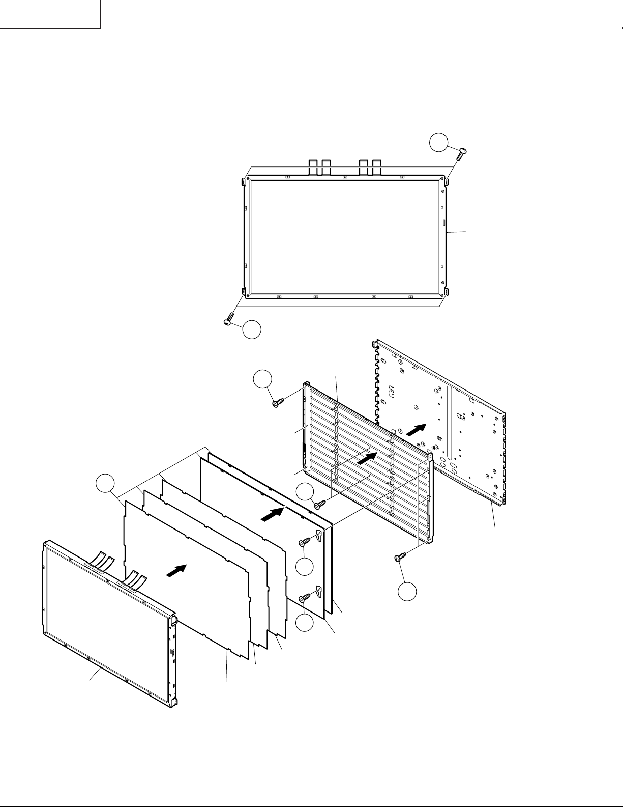
23.Take off the LCD panel with panel shield by removing 4 screws.
24.Take off D-BEF sheet, prism sheet and diffusion sheet. Take off ITO sheet and diffusion panel by removing 2
screws.
25.Take off the panel shield by removing 6 screws and 2 in the center.
23
LCD Panel
LCD Panel
24
23
25
Diffusion Sheet
Prism Sheet
D-BEF Sheet
25
24
24
Lamp
Panel Shield
25
Diffusion Panel
ITO Sheet
18
Page 19

LC-30HV4E
ADJUSTMENT PROCEDURES (AVC SYSTEM)
Preparation for adjustment
1. The product has been adjusted and optimized in the factory. If the product needs to be readjusted for some
reason, e.g., after parts replacement, follow the instructions shown below.
2. Control parameter values set in the in-process adjustment mode has been stored in the corresponding registers.
When the product is readjusted, the contents of the registers are changed. Bef ore readjustment, f actory settings
should be noted in case the contents of registers require to be restored.
3. Use a stabilized AC power supply.
4. To rewrite a program, you should note the items you want to change and initialize EEPROM, and then rewrite
the changes into EEPROM.
How to enter the in-process adjustment mode
CAUTION: Exercise great care to hide the procedure in entering the in-process adjustment mode from the
customer. Inadvertent setting changes in this mode may cause a fatal error resulting in a program being
unrecoverable.
1. Entering the in-process adjustment mode:
Connect the system cable between the display and AVC system.
Turn on the main power while holding down the "Input" button and the "Volume (down)" button simultaneously.
The system will be activated.
~If you see multiple lines of blue characters on the display, you are in the in-process adjustment mode. If not
(the normal activation screen opens), retry.
2. Accessing the inspection process mode:
After activation of the system, make adjustments according to the instructions indicated on the process adjustment
OSD menu screen.
Move to the General Process Adjustment (AVC System Section Process).
3. Restoring factory settings:
When the "INDUSTRY INIT" button is selected after activation of the system, factory channel setting remains
unchanged after the system exits from the in-process adjustment mode.
Changes made by the user will default to factory settings. Note that channel setting is also initialized.
4. Exiting from the in-process adjustment mode:
Unplug the power cable while the system is in the in-process adjustment mode to exit from the mode.
Take care not to press the "Power" button on the remote controller or the AVC system after using factory
settings to run the system.
5. OSD menu screen and menu items during manual adjustment:
~The layout and men u items of the OSD menu screen ma y some what vary depending on the program versions .
~Just rewriting a program does not cause settings to be "initial values". (Preparation for adjustment)
1. Button operation in the in-process adjustment mode
Cursor Up Move to the next page
Cursor Down Back to the previous page
Volume (High) Increase the setting by 1
Volume (Low) Decrease the setting by 1
Enter Execute the function
Cursor Left Increase the setting by 10
Cursor Right Decrease the setting by 10
Channel Select (Up) Move the cursor up
Channel Select (Down) Move the cursor down
Input Change Change input (Tuner -> Input 1 -> Input 2 ->Input 3 -> Input 4 -> PC ->)
19
Page 20
LC-30HV4E
2. In-process adjustment screen layout
Page Program version Color system
TUNER NO SIG1/13 HDCP:OFF EUROPE EUROPE
CENTER Version
OSD Version
CVIC Version
TTXP V ersion
∫ ∫
∫ ∫
∫ ∫
∫ ∫
6. Loading the backup data and setting HDCP when the PC I/F unit is replaced
Nearly all data including factory settings, user settings, and channel setting is stored in the PC I/F unit.
The product comes with EEPROM (IC1506) on the Main Unit in case the PC I/F unit is replaced; original data
backed up on the EEPROM can be loaded to the new PC I/F unit.
∫ How to load the backup data
Select EEPRON RECOVERT in the OSD menu (page 13/13) and turn the Volume key ON; then press
ENTER.
∫ How to set HDCP
After completion of adjustments, select KEY WRITE "ON" in the OSD men u (page 1/13) for man ual adjustment
and turn the Volume key ON; then press ENTER.
2001 06 21A
XXXXXXXX
XXXXXXXX
XXXXXXXX
∫
∫
∫
∫
Main unit AV unitHDCPSource of input
20
Page 21
ËË
Ë Adjustment parameters
ËË
1) Analog adjustment
(1) AVC System voltage adjustment
Adjustment items Adjustment conditions Adjustment procedures
1 In-process adjustment
mode
(
Check the destination.
)
LC-30HV4E
Using the In-process adjustment remote controller,
enter the in-process adjustments mode.
Check that the destination is EUROPE.
2 AVC center 3.3V
adjustment
3 AVC center 1.8V
adjustment
Connect a DC voltmeter to TP4
at the opening on the top of the
PC I/F unit.
Connect DC voltmeter to
TP1701.
Move the cursor to the [Ë+Badj3.3V] line and adjust
the TP4 voltage to 3.25±0.01V.
Move the cursor to the [Ë+BAdj1.8V] line and press
OK.
Adjustment is complete if [Ë+BAdj1.8V complete]
appears.
If ERR occurs, adjust pin 6 at CN9 on the PC I/F unit
so that 1.8V is reached.
(2) PAL signal adjustment
Adjustment items Adjustment conditions Adjustment procedures
1 Setup 1. Set colour system to “PAL”.
2. Select PAL source.
100% colour bar signal including 100% white, such
as split field colour bar
2 Tuner level adjustment 1. Adjust TP1101 so that the Y signal without the
Connect the oscilloscope to
TP1101.
chroma component should be 1.00 ±0.05 Vp-p
(between the bottom of sync signal and the white
peak).
21
Page 22
LC-30HV4E
(3) PAL signal adjustment
Adjustment items Adjustment conditions Adjustment procedures
1 MAIN PAL Y
CONTRAST
adjustment
2 MAIN PAL COLOR
GAIN adjustment
1. Adjust pin (1) of P801 to 0.70 ±0.025 Vp-p.
1. Adjust pin (3) of P801 to
0.70 ±0.025 Vp-p.
0.70V
3 MAIN CR GAIN PAL
adjustment
4 MAIN CONTRAST
adjustment
Press the DUAL screen button. Select the special DUAL screen settings for adjustment
5 SUB PAL Y adjustment 1. Adjust TB1274_SUB output (TP806) to
6 SUB PAL COLOR
GAIN adjustment
1. Adjust pin (5) of P801 to
0.70 ±0.025 Vp-p.
0.70V
Turn off the PEAK ACL control. Adjust the output
(TP815) of IC810 to have 0.90±0.025 Vp-p from the
pedestal level.
(so that the same video source is reflected on MAIN/
SUB).
1.5 ±0.05 Vp-p.
1. Adjust TB1274_SUB output (TP805) to
1.5 ±0.05 Vp-p.
(4) SECAM signal adjustment
Adjustment items Adjustment conditions Adjustment procedures
1 Setup 1. Set colour system to SECAM.
2. Select SECAM source.
100% colour bar signal including 100% white, such
as split colour color bar
2 MAIN SECAM Y
CONTRAST
adjustment
3 MAIN SECAM COLOR
GAIN adjustment
4 MAIN CR GAIN
SECAM adjustment
1. Adjust pin (1) of P801 to 0.70 ±0.025 Vp-p.
1. Adjust pin (3) of P801 to
0.70 ±0.025 Vp-p.
0.70V
1. Adjust pin (5) of P801 to
0.70 ±0.025 Vp-p.
0.70V
22
Page 23
(5) N358 signal adjustment
Adjustment items Adjustment conditions Adjustment procedures
1 Setup 1. Set colour system to N358.
2. Select N358 source.
100% SMPTE colour bar or similar colour bar
signal including 100% white.
LC-30HV4E
2 MAIN N358 Y
CONTRAST
adjustment
3 MAIN N358 COLOR
GAIN adjustment
4 MAIN CR GAIN N358
adjustment
5 MAIN N358 TINT
adjustment
1. Adjust pin (1) of P801 to 0.70 ±0.025 Vp-p.
1. Adjust pin (3) of P801 to
0.70 ±0.025 Vp-p.
0.70V
1. Adjust pin (5) of P801 to
0.70 ±0.025 Vp-p.
0.70V
1. Adjust TB1274_MAIN output (TP802) so that
waveform becomes as illustrated below:
Smoothed
(6) Component 15k Hz signal adjustment
Adjustment items Adjustment conditions Adjustment procedures
1 Setup 1. Select component 15k Hz.
2. Select component source.
100% colour bar signal including 100% white, like
split field colour bar
2 MAIN COMP 15k Y
Level adjustment
3 MAIN COMP 15k
COLOR GAIN
adjustment
4 MAIN CR GAIN COMP
15k adjustment
Adjust pin (1) of P801 to 0.7 0±0.025 Vp-p.
Adjust pin (3) of P801 to
0.70 ±0.025 Vp-p.
Adjust pin (5) of P801 to
0.70 ±0.025 Vp-p.
0.70V
0.70V
23
Page 24
LC-30HV4E
(7) Component HDTV signal adjustment
Adjustment items Adjustment conditions Adjustment procedures
1 Setup 1. Input HDTV (1080i) component signal.
2. Select component source.
100% colour bar signal including 100% white, like
split field colour bar
2 MAIN COMP HDTV
CONTRAST
adjustment
Turn off the PEAK ACL control.
Adjust the TP815 to have 0.90 ±0.25 Vp-p from the
pedestal level.
2. Factor y settings
(1) Factory Setting
Adjustment item Description Adjustment procedure
1 INDUSTRY INT
* Then turn off the AC power supply of the AVC system. (Be careful not to use the power switches of the remote control unit
and AVC system.)
24
Page 25
LC-30HV4E
In-process adjustment items
Do not change items, the adjustment procedure of which is not described in this manual. Inadvertent changes of
such items may result in unexpected or unrecoverable errors.
Page Item Page Item
Page 1
Page 3
Page 5
Page 7
Page 9
Page 11
Page 13
Maker Select
Ë+BAdj3.3V
Ë+BAdj1.8V(Enter: Auto)
KEY WRITE
ËDATA COPY
INDUSTRY INIT
CENTER V ersion
OSD V ersion
CVIC V ersion
TTXP V ersion
MONITOR V ersion
STANDBY TYPE
HOTEL MODE
ËSUB PAL Adjust
ËSUB PAL Y
ËSUB PAL COLOR GAIN
ËTUNER DAC ADJ
ËN358 Adjust
ËN358 Y CONTRAST
ËN358 COLOR GAIN
ËMAIN CR GAIN N358
ËN358 TINT
ËREFERENCE Adjust
ËPAL White Balance
PAL R CUTOFF
PAL R DRIVE
PAL G CUTOFF
PAL G DRIVE
PAL B CUTOFF
PAL B DRIVE
ËCOMP15K White Balance
COMP15K R CUTOFF
COMP15K R DRIVE
COMP15K G CUTOFF
COMP15K G DRIVE
COMP15K B CUTOFF
COMP15K B DRIVE
IPMODE INTERLACE
MDSW INTERLACE
PTGSW INTERLACE
IPMODE PROGRESSIVE
MDSW PROGRESSIVE
PTGSW PROGRESSIVE
IPMODE FMODEON
MDSW FMODEON
PTGSW FMODEON
IPMODE SUB
MDSW SUB
PTGSW SUB
IPMODE FMODEON PAL
MDSW FMODEON PAL
PTGSW FMODEON PAL
DEBUG PRINT SW
PIC ADJ MAKER SELECT
PIC ADJ KOUTEI SELECT
EEPROM SAVE
EEPROM RECOVER
DEBUG_SELECT_SW
DEBUG COMPANY SELECT
DEBUG PANELTYPE SELECT
CENTER PROG UPDATE
Page 2
Page 4
Page 6
Page 8
Page 10
Page 12
ËP AL Y CONTRAST
ËPAL COLOR GAIN
ËMAIN CR GAIN PAL
ËMAIN CONTRAST 15K
Center Acutime
RESET
Monitor Acutime
RESET
ËSECAM Adjust
ËSECAM Y CONTRAST
ËSECAM COLOR GAIN
ËMAIN CR GAIN SECAM
ËCOMP15K Adjust
ËCOMP15K Y CONTRAST
ËCOMP15K COLOR GAIN
ËMAIN CR GAIN COMP15K
ËCOMP HDTV Adjust
ËCOMP HDTV CONTRAST
ËCOMP HDTV SUB BRIGHT
ËPEAK ACL SW
ËN358 White Balance
N358 R CUTOFF
N358 R DRIVE
N358 G CUTOFF
N358 G DRIVE
N358 B CUTOFF
N358 B DRIVE
ËCOMP33K White Balance
COMPHDTV R CUTOFF
COMPHDTV R DRIVE
COMPHDTV G CUTOFF
COMPHDTV G DRIVE
COMPHDTV B CUTOFF
COMPHDTV B DRIVE
IPMODE PROGRESSIVE2
MDSW PROGRESSIVE2
PTGSW PROGRESSIVE2
IPMODE FMODEON2
MDSW FMODEON2
PTGSW FMODEON2
ILG LV
MD LV
VE LV
IP MODE SEL
25
Page 26

LC-30HV4E
UPGRADING INSTALLED PROGRAMS
Programs installed in the product are mainly divided into the following two categories:
∫ Main programs (for AVC system)
∫ Monitoring program (for display)
CAUTON: Exercise great care to hide the procedure in entering the in-process adjustment mode from the
customer. Inadvertent setting changes in this mode may cause a fatal error resulting in a program being
unrecoverable.
[Tools required]
∫ PC
A Windows 95/98/me/2000/XP PC that has a COM port (RS-232C).
A USB-R232C converter will be acceptable provided that it is appropriately set and has PC compatibility.
∫ RS-232C cross cable
Interlink cable is also acceptable.
[Preparations]
Rewriting a program needs the product to enter the in-process adjustment mode.
1) The re writing software is supplied in the f orm of an exe file named e .g., "MAIN_2002_10_10A.e xe" (pro visional).
Create a directory on a HD and copy the software into the directory.
2)Double-click the file. The file will be self-extracted. Check the extracted file against the documentation
accompanying with the software.
3) Connect the AVC System and the display unit with each other and make them ready f or operation (make sure
the power LEDs of the AVC System and display unit turn red).
4) Use an RS-232C cable to connect the PC to the AVC System.
5) Exercise great care to hide the procedure in entering the in-process adjustment mode from the customer.
Press the MAIN POWER button while holding down the volume DOWN key and the INPUT key on the display
unit simultaneously.
If blue characters appear on the display, the system has entered the in-process adjustment mode successfully.
If not (the normal activation screen opens), retry.
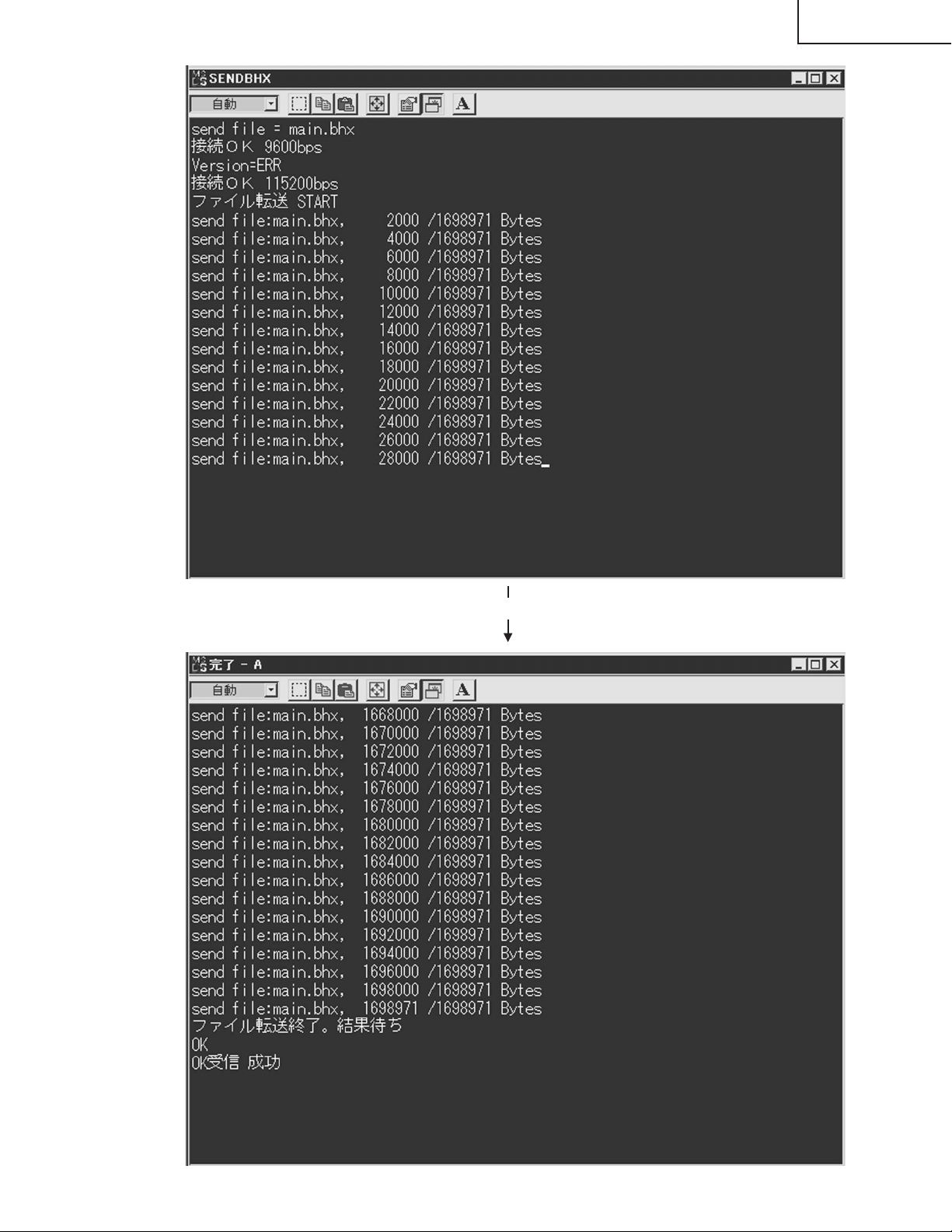
[Rewriting the main program]
1) In the in-process adjustment mode, press the Channel Up key on the remote controller. You will move to page
13 ("13/13" will appear on the upper left corner of the screen).
2) Make sure CENTER PROG UPDATE is highlighted.
3) Use the VOLUME -/+ keys to change OFF to ON.
4) Press the ENTER key on the remote controller. Characters on the screen will disappear and the screen blacks
out.
5) Double-click the batch file specified in the document accompanying with the software.
6) A black window (MS-DOS window) will open and rewriting starts automatically.
Rewiring of the main program is now complete. Unplug the AC cable from the AVC System and tur n off the
system and then on again.
7) Enter the in-process adjustment mode and make sure the version information on the CENTER Version, OSD
Version and CVIC Version lines on page 1 has been updated.
26
Page 27
LC-30HV4E
Continued
27
Page 28
LC-30HV4E
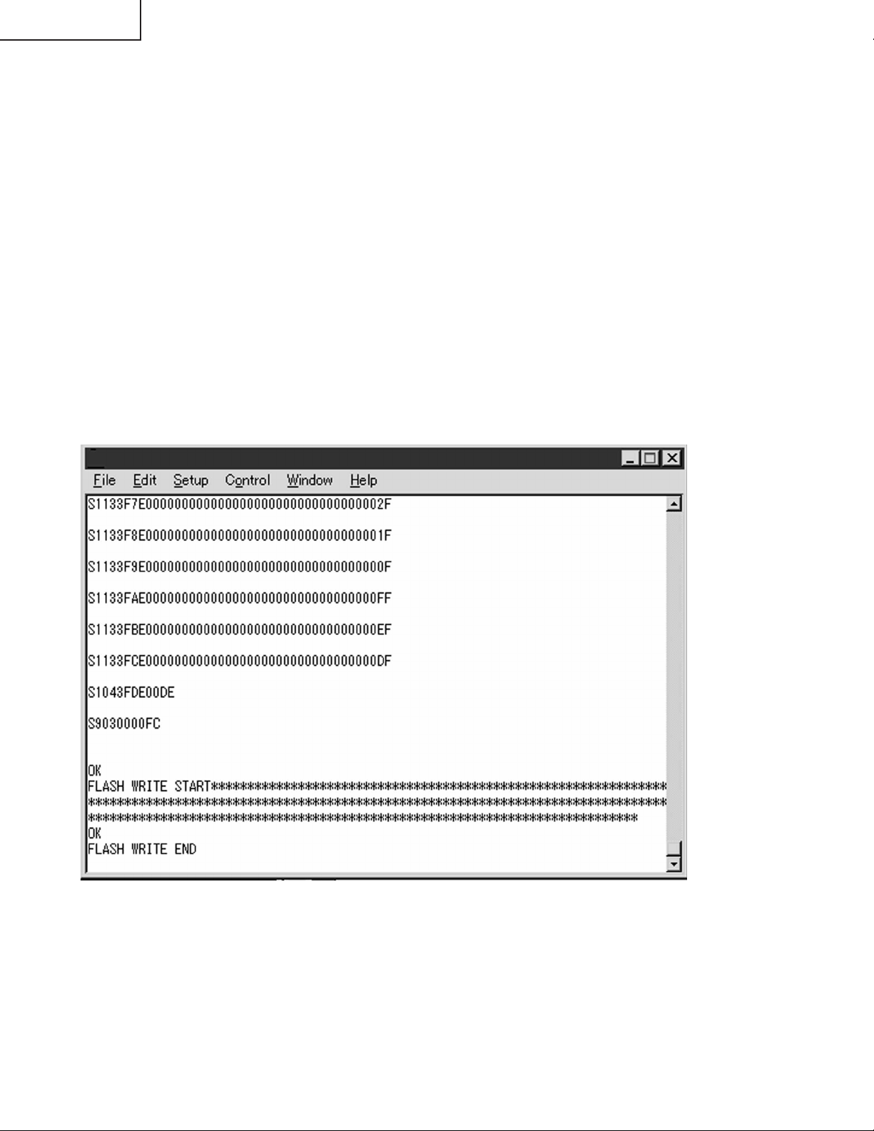
[Rewriting the monitor program]
1) Start terminal software in the in-process adjustment mode.
(Terminal software is not supplied. Use a freeware program available on the Internet.)
2) Set as follows:
Baud rate: 9600
Data length: 8 bits
Parity: None
Stop bit: 1
Flow control: None
3) If the settings are correct, pressing ENTER will cause ERR to appear on the screen.
4) Type "IPL_0002" and press ENTER. Characters on the screen will disappear and the screen blacks out.
* After the above string is entered, unusual indication may appear on the screen. This is not abnormal.
5) Press ENTER. The following will appear on the screen:
ERR
SEND "MONITOR PROG UPDATE PROGRAM" from PC to MR
6) Change the baud rate of the terminal software to 115200.
7) Use the file transfer facility of the terminal software to transfer the file specified in the document accompanying
with the rewriting software.
8)If the terminal software screen shows the following indication, the monitor program has been rewritten
successfully. (The indication will vary depending on the terminal software and program versions.)
9) Enter the in-process adjustment mode and make sure the version information on the MONITOR line has been
updated.
28
Page 29

LC-30HV4E
ADJUSTMENT PROCEDURES (DISPLAY)
See "Adjusting mode" for the steps to go into adjustment process mode.
1) +B adjustment (Digital PWB: R4648)
1. Receive PAL standard color bar signal.
2. Connect digital voltmeter to TP4602 and adjust to the specified value.
Specification: 13.00 ± 0.05V
2) Common bias adjustment
Make this adjustment each for "50 Hz", "60 Hz" and "PC". Select the input signal according to the indication onscreen.
1. Go to "Adjustment process mode".
2. On the LCD, select "14" of "PATTERN 1", dot inversion flicker pattern 2.
3. Then, select "COM BIAS" on the LCD.
4. Set the value so that the flicker on the screen is minimized.
Note: Apply this adjustment after for at least 30 min.
3) Background adjustment
1. Select video standard, and confirm the indication that the unit is preset to the standard.
2. At video input, receive the window pattern signal having left 80% WHITE and right 20% WHITE.
3. Set the screen size to the full mode.
4. Go to "Adjustment process mode".
5. Adjust "R OFFSET", "G OFFSET" and "B OFFSET" in "SIL861" so that left side 80% WHITE window pattern is
set to the specified value.
6. Adjust "R GAMMA", "G GAMMA" and "B GAMMA" in "SIL861" so that right side 20% WHITE window pattern is
set to the specified value.
Specification: x = 0.275 y = 0.273 (80% WHITE) x= 0.269 y = 0.253 (20% WHITE) [Minolta CA-110]
Note: Apply this adjustment after for at least 30 min.
4) Initialization
1. Go to "Adjustment process mode".
2. Select "1" thru "3" of "CLR MODE" in "TEST".
Setting range: 0 Normal
1 Initial setting (User clear: Factory setting)
2 Initial setting (All clear) Full initialization of EEPROM (except for ROM area)
3 Full initialization of Configuration EEPROM
3. Move the cursor down by one line.
4. Press "VOL UP" key and change the display from "WAIT" to "SEND" (write).
5. Do not shut down power while the display is "SEND".
6. When the writing is finished, the display changes from "SEND" to "WAIT".
5) Resetting lamp error counter
1. Go to "Adjustment process mode".
2. Select "L ERR RESET" in "TEST".
3. Reset the data to "0".
[L ERR RESET]
Function: Reset of fluorescent lamp error counter
It resets the times of fluorescent lamp errors and clears the last value in the memory.
Indication range: 0-5 (Fluorescent lamp errors)
(When lamp error exceeds 5 times, power supply is disabled. Resetting is required in this case.)
29
Page 30
LC-30HV4E
3.
Adjusting Mode
1. Overview
The controller IC can be adjusted in this mode.
Adjustment is done while controlling the setting of the resistor corresponding to the selected adjustment item.
When monitor is used independently, it is adjusted using the OSD simple display function incorporated in LCD
controller.
The OSD function of panel link receiver (SIL861) is used for adjustment of the independent monitor.
2. Entry to the mode
1) When cable is not connected (independent mode), follow the steps below.
a) When power switch is turned on, press the main unit INPUT and VOL DOWN keys simultaneously.
b) Press the remote controller's process adjustment key (R/C code: 40h) / process adjustment mode 2 key (R/
C code: 31h).
2) When not in independent mode, follow the steps below.
a) When power switch is turned on, press the main unit CH DOWN and VOL UP keys simultaneously.
b) Press the remote controller's process adjustment mode 2 key.
3. Exit from the mode
Turn off the power.
Press the remote controller's process adjustment mode 2 key.
4. Display
1) First layer display
The third line shows the title. The 5th line and below show the items. Microprocessor's version number
appears in the 16th line.
Example) 1.00 → 1 00
1234567891011121314
1SERVICE MODE
2OMODE 50HZ
3LCD
4SIL861
5TEST
6VERXXX
2) Second layer display (Adjustment item display)
A single page shows up to 10 adjustment items (or 14 lines).
The third line shows the title and the screen mode selected in MODE items (only when LCD is selected).
The 5th line shows the item. Microprocessor's version number appears in the 16th line.
Example) 1.00 → 1 00
Setting is shown in decimal number.
a) Adjustment on the LCD items
1234567891011121314
1LCD 50HZ
2OVL0 22 1
3REF0 209
4VL64 98
5REF64 170
6VL96 92
7REF96 184
8 VL128 85
9REF128 188
10 VL160 71
11 REF160 199
30
Page 31

b) Adjustment on the TEST items
1234567891011121314
1TEST
2OL ERR RE 0
3LCDDATA0000
4WAIT
5CLRMODE 0
6WAIT
7CNFGEEP0000
8WAIT
5. Changing data
In "adjustment item display", the items pointed by cursor can be changed using VOL UP/DOWN key.(Holding
down the key is effective.)
For the items in "LCD DATA", select the item and hit ENTER key. The ten's digit (leftmost digit) in the address
changes to red (others in green). Data change using VOL UP/DOWN key is enabled.
To move to the next digit, press CH UP key (or rightward cursor key). To go back to the previous digit, press CH
DOWN key (or leftward cursor key). Thus, 4 digits data can be entered.
When CH UP key is pressed while in rightmost digit, the cursor mov es to the leftmost digit. When CH DOWN key
is pressed while in leftmost digit, the cursor moves to the rightmost digit.
After address data adjustment, press ENTER key to exit from 4-digit adjustment and change the entire "LCD
DATA" line to red letters. (Same status as item selection)
LC-30HV4E
6. Key operation
1) Basic behaviors
Basic key behaviors are as follows.
Behavior Keys
Remote controller Main unit
Upward cursor movement Cursor up CH UP
Downward cursor movement Cursor down CH DOWN
Rightward cursor movement Cursor right
Leftward cursor movement Cursor left
Data UP VOL UP VOL UP
Data DOWN VOL DOWN VOL DOWN
Set ENTER INPUT
Back to previous layer RETURN
Back (In bottom layer only) ENTER INPUT
2) Data UP/DOWN
For the item for which OSD display is available, switch the display.
Adjust the data with UP/DOWN operation. (Any value beyond the limit is replaced by the limit value.)
Output data processing
Data transmission for every UP/DOWN operation (Data related to peripheral controller IC)
Execution of the last memory data when key is off
While the key is held down, the second step is performed approx. 500ms after the key operation and, after this,
every single step of UP/DOWN is carried out sequentially at 135ms interval.
3) Cursor UP/DOWN
Select the adjustment item by pointing it with the cursor.
When upward cursor movement is done while the cursor is at the top item, the cursor goes to the bottom item.
(In the case of multiple pages, the cursor goes to the bottom item on the previous page.)
When downward cursor mov ement is done while the cursor is at the bottom item, the cursor goes to the top item.
(In the case of multiple pages, the cursor goes to the top item on the next page.)
While the key is held down, the second step is performed approx. 500ms after the key operation and, after this,
every single step of UP/DOWN is carried out sequentially at 135ms interval.
31
Page 32

LC-30HV4E
ADJUSTMENT MODE MENU LIST
First layer item PAGE ITEM SETTING RANGE INITIAL VALUE DATA SETTING
MODE 1 50HZ/60HZ/PC 50HZ Toggle
LCD 1 VL0 0 ~ 255 221 No Toggle
REF0 0 ~ 255 209 No Toggle
VL64 0 ~ 255 98 No Toggle
REF64 0 ~ 255 170 No Toggle
VL96 0 ~ 255 92 No Toggle
REF96 0 ~ 255 184 No Toggle
VL128 0 ~ 255 85 No Toggle
REF128 0 ~ 255 188 No Toggle
VL160 0 ~ 255 71 No Toggle
REF160 0 ~ 255 199 No Toggle
2 VL192 0 ~ 255 77 No Toggle
REF192 0 ~ 255 103 No Toggle
VL224 0 ~ 255 88 No Toggle
REF224 0 ~ 255 112 No Toggle
VL256 0 ~ 255 108 No Toggle
REF256 0 ~ 255 78 No Toggle
COM BIAS 0 ~ 255 70 No Toggle
PWM CTRL 0 ~ 7 Toggle
PWM FREQ 0 ~ 4095 585 No Toggle
PWM DUTY 0 ~ 4095 0 No Toggle
3 PATTERN1 0 ~ 14 0 Toggle
PATTERN2 0 ~ 12 0 Toggle
P – CLK1 0 ~ 3 0 No Toggle
P – CLK2 0 ~ 7 0 No Toggle
OS SW 0 ~ 1 0 Toggle
OS D1 0 ~ 255 138 No Toggle
OS D2 0 ~ 255 167 No Toggle
OS D3 0 ~ 255 170 No Toggle
OPC LV0 0 ~ 85 0(40) No Toggle
OPC LV1 0 ~ 85 8(44) No Toggle
4 OPC LV2 0 ~ 85 16(48) No Toggle
OPC LV3 0 ~ 85 24(52 )No Toggle
OPC LV4 0 ~ 85 32(56) No Toggle
OPC LV5 0 ~ 85 40(60) No Toggle
OPC LV6 0 ~ 85 48(64) No Toggle
OPC LV7 0 ~ 85 56(68) No Toggle
OPC LV8 0 ~ 85 64(72) No Toggle
OPC LV9 0 ~ 85 72(76) No Toggle
OPC LV10 0 ~ 85 80(80) No Toggle
SIL861 1 R GAMMA 20 ~ 180 100 No Toggle
R OFFSET 0 ~ 510 256 No Toggle
G GAMMA 20 ~ 180 100 No Toggle
G OFFSET 0 ~ 510 256 No Toggle
B GAMMA 20 ~ 180 100 No Toggle
B OFFSET 0 ~ 510 256 No Toggle
TEST 1 L ERR RESET 0 ~ 5 0 Toggle
LCD DATA Four digits 0 ~ F 0 Toggle
WAIT/SEND WAIT ———
CLR MODE One digits 0 ~ 2 0 Toggle
WAIT/SEND WAIT ———
CNFG EEP Four digits 0 ~ F 0 Toggle
WAIT/SEND WAIT ———
* Values in the parentheses are with PC.
32
Page 33

LC-30HV4E
MAJOR IC FUNCTIONS INFORMATIONS
∫ IC2501 (MSP4418G)
IC for decoding audio signals.
It serves as an S-IF audio signal decoder and an audio data selector.
∫ IC2510 (IXA385WJ)
IC for controlling audio delay.
LC-30/37HV4E uses a frame buffer to process video signals. This results in delay in outputting video signals.
The IC delays output of audio signals to synchronize output of video and audio signals.
∫ IC1301 (CXA2069Q)
7-input, 3-output selector.
This IC selects all audio and video signals received from input terminals and the tuner, except those signals
that relates to PC and components.
Video signals delivered to the IC are sent to YC separation circuits IC401 (main) and IC402 (sub). Audio
signals are sent to the SR unit via IC2501 (sound processor).
∫ IC401 (MM1519XQ)
4-input, 3-output video selector for component input.
This IC receives AV3 component input, AV1/3 RGB input and teletext RGB signals. Its output is for main, sub
and component.
∫ IC1601 (SDA5550M)
Teletext processing microcomputer.
This IC receives vide signals, decodes teletext and outputs data in RGB format.
∫ IC401/IC402 (TC90A69)
Adaptive infield 3-line digital comb filter supporting both NTSC and PAL.
This IC is a high-precision Y/C 1 chip incorporating a CNR circuit and performs YC separation of the sub video
signals received from IC1301.
∫ IC403/IC404 (ML6428C1)
6.7 MHz low-pass filter.
∫ IC801/IC802 (TB1274AF)
IC for synchronous processing of video and chroma signals for PAL/NTSC/SECAM color TV.
Color demodulation is provided by a high-perf ormance image compensation circuit in the video section, a PAL/
NTSC/SECAM auto discrimination circuit in the chroma section, and a crystal that generates 4.43 MHz, 3.58
MHz and M/N-PAL clock signals.
This IC has a 4-channel YC signal input, 2-channel RGB signal input, and 2-channel chrominance signal input.
It receives main and sub chrominance signals from IC401 (main) and IC402 (sub) and delivers chrominance
signals via one-channel output.
∫ IC803 (CXA2101Q)
IC having a chrominance input integrated with a high-perf ormance image compensation circuit. Equipped with
circuits for processing baseband signals and RGB signals and a 4-channel video switch incorporating an H/V
synchronization signal processing circuit.
Input selection is done by INPUT-SEL (IIC BUS). Y, Pb, Pr and GBR of Ycb, Cr and HD and their H/V
synchronization signals are inputted to input pins of each channel.
Multi-scan facility permits acceptance of a horizontal scan line frequency range of 16 KHz to 60 KHz.
33
Page 34

LC-30HV4E
∫ IC1901 (IXA392WJ)
FPGA for synchronous processing
This IC selects synchronization signals and creates horizontal blanking signals.
∫ IC604 (TA1318AF)
IC for synchronous processing of TV component signals and measurement of frequency.
This IC incorporates an input signal frequency measurement feature and synchronous regeneration features.
It supports synchronous horizontal regeneration (15.75 KHz, 31.5 KHZ, 33.75 KHz and 45 KHz) and synchronous
vertical regeneration (525I, 525P, 625I and 750P).
PC I/F board side
∫ IC4 (CX3506R)
3-channel, 8-bit, 120 MSPS A/D converter incorporating AMP and PLL.
This IC is for video signals inputted to the IF board and used for one-screen and two-screen applications, and
for PC signals inputted to the front panel.
It provides A/D conversion of video signals (analog RGB) inputted to IN1 from CN6 and PC signals (analog
RGB) inputted to IN2 from CN8.
Converted digital signals are sent to IC25.
∫ IC310 (TLC5733A)
3-channel, 8-bit, 20 MSPS A/D converter.
This IC is for video signals inputted to the IF board and used for two-screen application.
It provides A/D conversion of video signals (analog YcbCr) inputted to IC310 from CN6.
Converted digital signals are sent to IC25.
∫ IC25 (IXA091WJ)
IC for I/P conversion and scaling of digital image according to the output resolution, and for data conversion.
There are two input channel: V0 and V1. V1 is for sub 480i/580i input processing for two-screen application. V0
is for processing all signals for main used for one and two-screen applications.
The IC generates clamp signals based on input synchronization signals.
It also performs data matrix conversion, and creates OSD signals.
Processed signals are sent to IC413.
∫ IC413 (SiI170)
Panel link transmitter.
This IC converts 8-bit RGB image data received from IC25 into TMDS differential signals and sends to the
monitor.
∫ IC1 (IX8270CE)
One-chip RISC microprocessor.
This IC communicates with the monitor and controls the system operation.
It controls all the ICs located in the media receiver.
∫ IC405 (UPD4721G)
RS-232 line driver/receiver conforming to EIA/TIA-232-E.
This IC enables the system to be controlled from a PC connected to the system.
It also allows IC1 to be upgraded using the PC.
34
Page 35

ËRH-iXA385WJZZ (ASSY:IC2510)
» Pin mapping
Pin No. Pin Name Type Description
1, 19, 32, 33 VDD –– Power supply
44, 64
2 PLLVDC –– PLL power supply
3 VCOIN I VCO IN (used to construct external loop filter)
4 TEST I Input for testing
5 CPOUT O Charge pump out (used to construct external loop filter)
6 PLLEN I PLL enable signal input
7 PLLGND ––
8, 9, 10, 18, 31 GND ––
41, 42, 43, 62
11 PLLENO O PLL enable signal output
12 SPDIFO O S/PDIF output (3.072 Mbps)
13 SPDIFI I S/PDIF input (3.072 Mbps)
14 IO0 I/O Expanded I/O, bit 0
15 IO1 I/O Expanded I/O, bit 1
16 IO2 I/O Expanded I/O, bit 2
17 IO3 I/O Expanded I/O, bit 3
20 IO4 I/O Expanded I/O, bit 4
21 UTEST I Input for testing
22 NANDTO O Output for testing
23 RESET I Asynchronous reset signal input
24 MEMTEST I Input for testing
25 BISTOUT O Output for testing
26 RWCLK O Expanded FIFO R/W clock
27 RSTRW O Expanded FIFO master reset
28 FEW O Expanded FIFO write enable
29 FRE O Expanded FIFO read enable
30 FD07 O Expanded FIFO data output, bit 7
34 FD06 O Expanded FIFO data output, bit 6
35 FD05 O Expanded FIFO data output, bit 5
36 FD04 O Expanded FIFO data output, bit 4
37 FD03 O Expanded FIFO data output, bit 3
38 FD02 O Expanded FIFO data output, bit 2
39 FD01 O Expanded FIFO data output, bit 1
40 FD00 O Expanded FIFO data output, bit 0
45 FD17 I Expanded FIFO data input, bit 7
46 FD16 I Expanded FIFO data input, bit 6
47 FD15 I Expanded FIFO data input, bit 5
48 FD14 I Expanded FIFO data input, bit 4
49 FD13 I Expanded FIFO data input, bit 3
50 FD12 I Expanded FIFO data input, bit 2
51 FD11 I Expanded FIFO data input, bit 1
52 FD10 I Expanded FIFO data input, bit 0
53 SDA I/O Serial communication data
54 SCS I Serial communication chip select
55 SCK I Serial communication chip select
56 I2SCLO O 12S CL output
57 I2SDAO O 12S CL output
58 I2SWSO O 12S WS output
59 I2SWSI I 12S WS input
60 I2SDAI I 12S DA input
61 I2SCLI I 12S CL input
63 REFCLK I PLL REF CLK (same input as 12SCLI)
LC-30HV4E
35
Page 36

LC-30HV4E
36
Page 37

» Pin mapping
Pin No. Pin Name Type Description
1 NC –– Not connected
2 I2C_CL I/O I2C clock
3 I2C_DA I/O I2C data
4 I2S_CL I/O I2S clock
5 I2S_WS I/O I2S word strobe
6 I2S_DA_OUT O I2S data output
7 I2S_DA_IN1 I I2S1 data input
8 ADR_DA O ADR data output
9 ADR_WS O ADR word strobe
10 ADR_CL O ADR clock
11, 12, 13 DVSUP –– Digital power supply 5V
14, 15, 16 DVSS –– Digital ground
17 I2S_DA_IN2 I I2S2-data input
18 NC –– Not connected
19 I2S_CL3 I I2S3 clock
20 I2S_WS3 I I2S3 word strobs
21 RESETQ I Power-on-reset
22 I2S_DA_IN3 I I2S3-data input
23 NC –– Not connected
24 DACA_R O Headphone out, right
25 DACA_L O Headphone out, left
26 VREF2 –– Reference ground 2
27 DACM_R O Loudspeaker out, right
28 DACM_L O Loudspeaker out, left
29, 30, 31, 32 NC –– Not connected
33 SC2_OUT_R O SCART 2 output, right
34 SC2_OUT_L O SCART 2 output, left
35 VREF1 –– Reference ground 1
36 SC1_OUT_R O SCART 1 output, right
37 SC1_OUT_L O SCART 1 output, left
38 CAPL_A –– Volume capacitor AUX
39 AHVSUP –– Analog power supply 8V
40 CAPL_M –– Volume capacitor MAIN
41,42 NC –– Not connected
43,44 AHVSS –– Analog ground
45 AGNDC –– Analog reference voltage
46 NC –– Not connected
47 SC4_IN_L I SCART 4 input, left
48 SC4_IN_R I SCART 4 input, right
49 ASG –– Analog Shield Ground
50 SC3_IN_L I SCART 3 input, left
51 SC3_IN_R I SCART 3 input, right
52 ASG –– Analog Shield Ground
53 SC2_IN_L I SCART 2 input, left
54 SC2_IN_R I SCART 2 input, right
55 ASG –– Analog Shield Ground
56 SC1_IN_L I SCART 1 input, left
57 SC1_IN_R I SCART 1 input, right
58 VREFTOP –– Reference voltage IF A/D converter
59 NC –– Not connected
60 MONO_IN I Mono input
61, 62 AVSS –– Analog ground
63, 64 NC –– Not connected
65, 66 AVSUP –– Analog power supply 5V
67 ANA_IN1+ I IF input 1
68 ANA_IN- I IF common(can be left vacant, only if IF input 1 is also not in use)
69 ANA_IN2+ I IF input 2(can be left vacant, only if IF input 1 is also not in use)
70 TESTEN I Test pin
71 XTAL_IN I Crystal oscillator
72 XTAL_OUT O
73 TP –– Test pin
74 AUD_CL_OUT O Audio clock output(18.432MHz)
75, 76 NC –– Not connected
77 D_CTR_I/O_1 I/O D_CTR_I/O_1
78 D_CTR_I/O_0 I/O D_CTR_I/O_0
79 ADR_SEL I I2C Bus address select
80 STANDBYQ I Stand-by(low-active)
LC-30HV4E
37
Page 38

LC-30HV4E
ËVHiCXA2069Q-1 (ASSY:FIC1301)
S2-compatible 7-input, 3-output AV switch
»Block diagram
38
Page 39

» Pin mapping
Pin No. Pin Name Type Description
63 TV I Video signal input
1 V1 I Composite video signal input
8V2 I
15 V3 I
22 V4 I
30 V4 I
60 V4 I
3 Y1 I Y/C separation signal input, used for luminance signal input
10 Y2 I YIN1: Input for signal created by Y/C separation of VOUT1 output
17 Y3 I
24 Y4 I
49 YIN1 I
5 C1 I Y/C separation signal input, used for chrominance signal input
12 C2 I CIN1: Input for signal created by Y/C separation of VOUT1 output
19 C3 I
26 C4 I
51 CIN1 I
62, 2 LTV, LV1 I Audio signal input
9, 16 LV2, LV3 I
23, 29 LV4, LV5 I
59, 64 LV6, RTV I
4, 11 RV1, RV2 I
18, 25 RV3, RV4 I
31, 61 RV5, RV6 I
53 VOUT1 O Video signal output, used for composite vide signal output
41 VOUT3 O
44 V/YOUT2 O Video signal output, controlled via 12C bus and used for composite video signal output
56 YOUT1 O Power or luminance signal output is selected.
39 YOUT3 O Video signal output, used for luminance signal output
58 COUT1 O Video signal output, used for chrominance signal output
47 COUT2 O
37 COUT3 O
52 LOUT1 O Audis signal output
43 LOUT2 O
38 LOUT3 O
54 ROUT1 O
45 ROUT2 O
40 ROUT3 O
6 S2-1 I Used for detection of S2-compatible DC that is superimposed to C signal.
13 S2-2 I 4:3 image signal is selected when voltage ? 1.3V, 4:3 letterbox signal when 1.3V
20 S2-3 I < voltage ? 2.5V, and 16:9 squeeze signal when voltage > 2.5V. 4:3 image signal is
27 S2-4 I selected when the pins are open because they are pulled down to GND via 100K?.
7 S-1 I Used for selection between composite video signal and S signal.
14 S-2 I Detection result is written to the status register. S signal is selected when voltage ?
21 S-3 I 3.5V, and composite video signal when voltage > 3.5V. Composite video signal is
28 S-4 I selected when the pins are open because they are pulled down to 5V via 100K?.
32 ADR I Used for selection of slave address for 12C bus.
90H is selected when voltage ? 1.5V, and 92H when ? 2.5V.
90H is selected when the pin are open.
33 SCL I 12C bus signal input
34 SDA I 12C bus signal input
36 DC OUT O Used for output of S2-compatible DC that is superimposed to COUT3.
DC superimposition is done by connecting to COUT3 via capacitor. The pin is
controlled via 12C bus.
Connection of 4.7k? external resistor provides output impedance of 10?3K? that
conforms to S2.
55 TRAP1 I Connected to trap circuit for sub carrier.
46 TRAP2 I
48 MUTE I Mute for audio signal output.
Mute is on when voltage ? 1.3V and off when voltage ? 2.5V.
Mute is off when the pin is open.
50 BIAS I Internal reference bias input.
Connected to GND via capacitor.
LC-30HV4E
39
Page 40

LC-30HV4E
ËVHiMM1519XQ-1 (IC1401)
Component Input Video Switch
»Block diagram
40
Page 41
» Pin mapping
Pin No. Pin Name Type Description
1 VIDEO 1-L1 I D-pin connection line input
2 VIDEO 1-L2 I
3 VIDEO 1-L3 I
11 VIDEO 2-L1 I
12 VIDEO 2-L2 I
13 VIDEO 2-L3 I
21 VIDEO 3-L1 I
22 VIDEO 3-L2 I
23 VIDEO 3-L3 I
4, 14, 39,45, 52, 58 VCC –– Analog power supply (9V)
51 AVCC ––
5 VIDEO 2-Y I Y signal input
15 VIDEO 3-Y I
53 TUNER-Y I
59 VIDEO 1-Y I
24 DGND ––
6, 8, 16, 18, 33,35, GND ––
37, 41, 43, 47, 49,
54, 58, 60, 62
7 VIDEO 2-Pb I Chrominance input
9 VIDEO 2-Pr I
17 VIDEO 3-Pb I
19 VIDEO 3-Pr I
55 TUNER-Pb I
57 TUNER-Pr I
61 VIDEO 1-Pb I
63 VIDEO 1-Pr I
10 VIDEO 2-SW I D-pin connection check switch line input
20 VIDEO 3-SW I
32 MONO-SW I
64 VIDEO 1-SW I
25 ADDRESS I Slave address input
26 SDA I/O 12C bus data input/output
27 SCL I 12C bus clock input
28 DVCC –– Digital power supply (5V)
29 L3 OUT O Monitor output line output
30 L2 OUT O
31 L1 OUT O
34 Pr OUT 3 O Image output
36 Pb OUT 3 O
38 Y OUT 3 O
40 Pr OUT 2 O
42 Pb OUT 2 O
44 Y OUT 2 O
46 Pr OUT 1 O
48 Pb OUT 1 O
50 Y OUT 1 O
LC-30HV4E
41
Page 42

LC-30HV4E
ËVHiTB1274AF-1Q (ASSY:IC801, IC802)
VIDEO/CHROMA Processor
»Block diagram
42
Page 43

» Pin mapping
Pin No. Pin Name Type Description
1 CVBS1/Y1-IN I CVBS1 or Y1-IN signal input
2 SYNC-IN I Synchronization signal input
3 CVBS-OUT O CVBS or Y+C signal output
4 VS O Output of counted-down vertical synchronization signal
5 COMB Y-IN I Input of Y signal outputted from comb filter. Open when not used
6 D-VDD –– 5 VDC power supply to DDS/BUS/V-CD/H-CD block (standard)
7 COMB C-IN I Input of C signal outputted from comb filter. Open when not used
8 D-GND –– GND for DDS/BUS/V-CD/H-CD block
9 HS O Output of horizontal synchronization signal under AFC
10 SCP O Sand castle pulse output.
Clamp pulse and horizontal blanking pulse are outputted.
11 Yvi-IN O Output of synchronous input Y signal selected using video SW
12 SYNC-VCC –– 5VDC power supply to SYNC/HVCO block (standard)
13 SCL I 12C bus SCL input
14 SDA I/O 12C bus SDA output
15 YS3 I Switch for selection between main signal and RGB1 input signal. This input is
(iRGB1-in) operative only when RGB1-ENB is enabled during bus setting.
16 SYNC-GND –– GND for SYCN/HVOC block
17 Cr1-IN I Y1/Cb/Cr1 signal input
18 Cb1-IN I
19 Y1-IN I
20 CLP-FIL –– Used to connect Y clamp filter
21 Y-OUT O Y/Cb/Cr signal output
22 Cb-OUT O
23 Cr-OUT O
24 YS1 I Switch for selection between main signal and input signal
(YVbC2-IN)
25 B1-IN I RGB1 signal input. YS3 or 12C bus is used to select signal.
26 G1-IN I
27 R1-IN I
28 Y/C-GND –– GND for Y/C/Text/Video-SW/1HDL block
29 Cr2-IN I Y2/Cb2/Cr2 signal input. YS1 is used to select signal.
30 Cb2-IN I Open when the pin is not used.
31 Y2-IN I
32 Y/C-VCC –– 5VDC Power supply to Y/C/Text/Video-SW/1HDI block. (standard)
33 B2-IN I RGB2 signal input. YS is used to select signal.
34 G2-IN I Open when not used.
35 R2-IN I
36 YS2/YM I Switch for selection between main signal and RGB2 input signal
(RGB2-IN)
37 FIL. –– Connected to Y/C-VCC pin
38 X'TAL –– Connect to 16.2 MHz crystal oscillator
39 C3-IN I Chroma signal input. Open when not used.
40 APC-FIL –– Connected to chroma modulation filter
41 CVBS3/Y3-IN I CVBS33 or Y3 signal input. Open when not used.
42 ADDRESS I Slave address input
43 C2-IN I Chroma signal input. Open when not used.
44 CVBS2/Y2-IN I CVBS2 or Y2 signal input. Open when not used.
45 COMB SYS O Current color system discrimination result output. Pin 46 is also used for this output.
46 Fsc-OUT O Sub carrier output
47 AFC-FIL –– Connected to AFC detection filter
48 C1-IN I Chroma signal input. Open when not used.
LC-30HV4E
43
Page 44

LC-30HV4E
ËVHiCXA2101Q-1 (ASSY:IC803)
Baseband image signal processing
»Block diagram
44
Page 45

» Pin mapping
Pin No. Pin Name Type Description
1 IN2-H I IN2-H: Independent H periodic signal input
2 IN2-V I IN2-V: Independent V periodic signal input
3 IN2-1 I IN2 system signal input
4 IN2-2 I
5 IN2-3 I
6 Vcc-MAT –– Power supply to selector or synchronous processing modules
7 IN3-H I IN3-H: Independent H periodic signal input
8 IN3-V I IN3-V: Independent V periodic signal input
9 IN3-1 I IN3 system signal input
10 IN3-2 I
11 IN3-3 I
12 GND-MAT –– GND for selector or synchronous processing modules
13 IN4-H I IN4-H: Independent H periodic signal input
14 IN4-V I IN4-V: Independent V periodic signal input
15 IN4-1 I IN4 system signal input
16 IN4-2 I
17 IN4-3 I
18 V-PH Connected to capacitor for holding Vsync peak
19 IN5-H I IN5-H: Independent H periodic signal input
20 IN5-V I IN5-V: Independent V periodic signal input
21 IN5-1 I IN5 system signal input
22 IN5-2 I
23 IN5-3 I
24 H-PH Connected to capacitor for holding Hsync peak
25 YG-OUT O Output of composite video signal for synchronous separation
26 YG-IN I Input of composite video signal for synchronous separation
27 IREF-SYNC Pin for reference current setting (approx. 4.6V)
28 VS-OUT O Output of HV of either IN1 system or IN2 ? IN5 system selector signals. Signal is
29 HS-OUT O selected by 12C bus "YCBCR/MAT".
30 Vcc-OUT O Power supply to RGB system
31 SCP-IN I Sand-castle-pulse input
32 VTIM-IN I V timing pulse input
33 HP-IN I H pulse input
34 GND-OUT O GND for RGB system
35 R-OUT O RGB signal output.
37 G-OUT O When 100IRE white is inputted, signal is outputted at 2.6Vp-p.
39 B-OUT O
36 R-SH RGB AKB sample & hold
38 G-SH
40 B-SH
41 IK-IN I Input of returned reference pulse
42 PABL-FIL Peak ABL peak-hold
43 ABL-FIL Creates LPF when ABL control signal is received.
44 ABL-IN ABL control signal input
45 ABL-IN YM1/YS1 control signal input.
46 LR1-IN I Analog RGB1 signal input
47 LG1-IN I
48 LB1-IN I
49 LB1-IN I YM2/YS2 control signal input.
50 LR2-IN I Analog RGB2 signal input
51 LG2-IN I
52 LB2-IN I
53 ADDRESS I 12C bus slave address input
54 DPIC-C I Used to connect capacitor to GND pair for detection of dynamic picture
55 SCL I 12C bus SCl (serial clock) input
56 SCL I 12C bus SDA (serial data) input
57 DPIC-MUTE I Used to provide mute control to dynamic picture (black expansion)
58 CLP-C Connected to Y system clamp capacitor
59 VM-OUT O VM output. Differential waveform of Y signal is outputted with positive polarity.
60
61 YCBCR-SW I Input for switching signal inputted to INT/EXT SW. External input pin is selected when
62 ECR-IN I External Y/Cb/Cr signal input
63 ECB-IN I
64 EY-IN I
VM/SHP/COL-OFF Used to turn off VM, sharpness and color. Input level is judged on the three-value logic.
Input level is judged on the three-value logic.
This pin enables VM to turn off when YM or YS reaches its specified value.
Input level is judged on the three-value logic.
This pin enables VM to turn off when YM or YS reaches its specified value.
(black expansion)
this input is High.
LC-30HV4E
45
Page 46

LC-30HV4E
ËRH-iXA385WJZZ (ASSY:IC2510)
» Pin mapping
Pin No. Pin Name Type Description
1 NC –– Non-connection
2 SP_CP2 I Input of clamp signal from synchronous separation IC (for 15K system)
3 SP_VD I Input of vertical synchronization signal from synchronous separation IC
4 GND –– Ground
5 SP_HD I Input of horizontal synchronization signal from synchronous separation IC
6 VD3 O Output of vertical synchronization signal to synchronous separation IC
7 HD3 O Output of horizontal synchronization signal to synchronous separation IC
8 SP_CP1 I Input of clamp signal from synchronous separation IC (normal)
9 TDI I SP data input
10 TMS I SP mode input
11 TCK I SP clock input
12 TEXT_HD O TEXT_HD output
13 US_HD I RCA/TEXT horizontal synchronization signal input
14 TEXT_VD O TEXT_VD output
15 Vcc3.3V –– TEXT_VD output
16 US_VD I RCA/TEXT vertical synchronization signal input
17 GND –– Ground
18 MODEA I Mode selection signal A
19 MODEB I Mode selection signal B
20 MODEC I Mode selection signal C
21 SELA I Input of HD switching control signal for main video chroma/RCA
22 SELO I Input of control signal for TEXT synchronization signal output
23 SELC I Input of control signal for TEXT synchronization signal output
24 TDO O ISP data output
25 GND –– Ground
26 Vcc3.3V –– Power supply
27 VD1 I Input of vertical synchronization signal from main video chroma IC
28 HD1 I Input of horizontal synchronization signal from main video chroma IC
29 PL_VD O Vertical synchronization signal output
30 PL_HD O Horizontal synchronization signal output
31 PL_CP O Clamp signal output
32 PL_BLK O H blank signal output
33 MODED I Mode selection signal D
34 NC –– Mode selection signal D
35 Vcc3.3V –– Power supply
36 NC –– Non-connection
37 CC_HD O Horizontal synchronization signal for closed caption
38 ow_vblk I Auto wide V blank signal input
39 HDS O Output of horizontal synchronization signal for PC board
40 VDS O Output of vertical synchronization signal for PC board
41 HD2 I Input of horizontal synchronization signal from sub video chroma IC
42 VD2 I Input of vertical synchronization signal from sub video chroma IC
43 clk I Clock input
44 NC –– Non-connection
46
Page 47

ËVHiTC90A69++1Y (ASSY:IC402)
» Pin mapping
Pin No. Pin Name Type Description
1 BIAS –– ADC bias
2 VRT –– ADC upper limit bias
3 VDD1 –– ADC and DAC power supply (analog system)
4 TESTI1 I Input for testing
5 VSS2 –– ADC GND (analog system)
6 VRB –– Video signal input
7 YCIN I ADC lower limit bias
8 TEST O Reset control and test control before shipping
9 KILLER I Y/C separation and vertical enhancer OFF
10 TESTI2 I Input for testing
11 VDD3 –– Power supply to logic (digital system)
12 VSS3 –– Logic and DRAM GND (digital system)
13 VDD2 –– DRAM power supply (digital system)
14 TESTI3 I Input for testing
15 SCL I IIC BUS clock input
16 SDA I IIC BUS data input
17 MODE1 O MODE1 output
18 TESTOUT I Input for testing
19 FSC I Clock input
20 VDD4 –– PLL power supply (analog system)
21 VSS4 –– PLL GND (analog system)
22 FIL I VCO control
23 PD O PLL detection output
24 VB2 –– DAC bias 2
25 YOUT O Luminance signal output
26 VSS1 –– DAC GND (analog system)
27 COUT O DAC GND (analog system)
28 VB1 –– DAC bias 1
LC-30HV4E
47
Page 48

LC-30HV4E
ËRH-iX3270CEZZ (ASSY:IC1)
» Pin mapping
Pin No. Pin Name Type Description
34, 36-44, D[15:0] I/O Data bus D [15:0]
46, 48-52
23-26, 28, 30-32 D[23:16/PTA[7:0] I/O Data bus D [23:16] / I/O port A [7:0]
13-18, 20, 22 D[31:24/PTB[7:0] I/O Data bus D [31:24] / I/O port B [7:0]
86, 84, 82, 78-72, A[25:0] O Address bus A [15:0]
70-68-60, 56-53
96 CS0 O Chip select 0/
98 CS2/PTK[0] O/(I/O) Chip select 2 / I/O port K [0]
99 CS3/PTK[1] O/(I/O) Chip select 3 / I/O port K [1]
100 CS4/PTK[2] O/(I/O) Chip select 4 / I/O port K [2]
101 CS5/CE1E/PTK[3] O/(I/O) Chip select 5 / CE1 (area 5SPCMIA)/O port K [3]
102 CS6/CE1B O Chip select 6 / CE1 (area 6SPCMIA)
87 BS/PTK[4] O/(I/O) Bus cycle start signal / I/O port K [4]
118 RAS3U/PTE[2] O/(I/O) RAS (area 3DRAM, SDRAM upper 32MB address) / I/O port E [2]
106 RAS3L/PTJ[0] O/(I/O) RAS (area 3DRAM, SDRAM upper 32MB address) / I/O port J [0]
119 RAS2U/PTE[1] O/(I/O) RAS (area 2DRAM, SDRAM upper 32MB address) / I/O port E [1]
107 RAS2L/PTJ[1] O/(I/O) RAS (area 2DRAM, SDRAM upper 32MB address) / I/O port JE [1]
108
110 CASLH/PTJ[3] O/(I/O) D15-D18 CAS (DRAM) / I/O port J [3]
112 CASHL/PTJ[4] O/(I/O) D23-D16 CAS (DRAM) / I/O port J [4]
113 CASHH/PTJ[5] O/(I/O) D31-D24 CAS (DRAM) / I/O port J [5]
116 CAS2L/PTE[6] O/(I/O) D31-D24 CAS (DRAM) / I/O port J [5]
117 CAS2H/PTE[3] O/(I/O) D31-D24 CAS (DRAM) / I/O port J [5]
89 WE0/DQMLL O D7-D0 selection signal/DQM (SDRAM)
90 WE1/DQMLU/WE O D7-D0 selection signal/DQM (SDRAM)
91 WE2/DQMUL/ O/(I/O) D23-D16 selection signal/DQM (SDRAM)/PCMCIA I/O port K [6]
92 WE3/DQMUU/ O/(I/O) D31-D24 selection signal/DQM (SDRAM)/PCMCIA I/O write I/O port K [7]
93 RD/WR O Read/Write switch signal
88 RD O Read strobe
105 CKE/PTK[5] O/(I/O) CK enable (for SDRAM only) / I/O port K [5]
123 WAIT I Hardware wait request
11-8 IRL[3:0]/IRQ[3:0]/ I Hardware wait request
12 IRQ4/PTH[4] I External interrupt request / I/O port H [4]
7 NMI I Non-maskable interrupt request
160 IRQOUT O Interrupt request output
182 WAKEUP/PTD[3] O/(I/O) Standby mode interrupt request output / I/O ports D [3]
159 TCLK/PTH[7] I/O TMU/RTC clock I/O / I/O port H [7]
191 DREQ0/PTD[4] I DMA request 0 / I/O port D [4]
114 DACK0/PTD[5] O/(I/O) DMA ACK 0 / I/O port D [5]
192 DREQ1/PTD[6] I DMA request 0 / I/O port D [6]
115 DACK1/PTD[7] O/(I/O) DMA ACK 1 / I/O port D [7]
189 DRAK0/PTD[1] O/(I/O) DMA ACK 1 / I/O port D [7]
190 DRAK1/PTD[0] O/(I/O) DMA ACK 0 / I/O port D [0]
171 RxD0/SCPT[0] I Receive data 0/SCI input port [0]
164 TxD0/SCPT[0] O Send data 0/SCI output port [0]
165 SCK0/SCPT[1] I/O Serial clock 0/SCI I/O port [1]
172 RxD1/SCPT[2] I Receive data 0/SCI input port [2]
166 TxD1/SCPT[2] O Send data 0/SCI output port [2]
167 SCK1/SCPT[1] I/O Serial clock 1/SCI I/O port [3]
174 RxD2/SCPT[4] I Receive data 0/SCI input port [4]
168 TxD2/SCPT[4] O Send data 2/SCI output port [4]
169 SCK2/SCPT[5] I/O Serial clock 2/SCI I/O port [5]
170 RTS2/SCPT[6] O/(I/O) Send request 2/SCI I/O port [6]
176
104 CE2B/PTE[5] O/(I/O) PC card 0 chip enable 2 / I/O port E [5]
126 IOIS16/PTG[7] I Write protect/input port G [7]
103 CE2A/PTE[[4] O/(I/O) PC card 1 chip enable 2 / I/O port E [4]
146, 149 CAP[1:2] –– PLL external capacitor pin [1:2]
156 EXTAL I External clock/crystal oscillator input
155 XTAL O Crystal oscillator output
162 CKIO I/O System clock I/O
5 EXTAL2 I RTC crystal oscillator input
4 XTAL O RTC crystal oscillator output
CASLL/CAS/PTJ[2]
ICIORD/PTK[6]
ICIOWR/PTK[7]
PTH[3:0]
CTS2/IRQ5/SCPT[7]
O/(I/O) D7-D0 CAS (DRAM)/CAS (SDRAM) / I/O port J [2]
I Send clear 2/enternal interrupt request/SCI input port [7]
48
Page 49

» Pin mapping
Pin No. Pin Name Type Description
193 RESETP I Power-on reset request
124 RESETM I Manual reset request
122 BREQ I Bus request
121 BACK O Bus ACK
2, 1, 144 MD[2:0] I Clock mode select
196, 195 MD[4:3] I Area 0 bus width select
197 MD5 I Endian select
194 CA O Chip active
158, 157 STATUS[1:0]/ I/O Processor status [1:0] / I/O port J [7:6]
204-199 AN[5:0]/PTL[6:7] I A/D converter input [5:0]/input port L [5:0]
206, 207 AN[6:7]/DA[1:0]/ I/O A/D converter input [6:7] / D/A converter output [1:0] / input port L [6:7]
177-180, 185-188 PTC[7:0]/PINT[7:0] I/O I/O port C [7:0]/port interrupt [7:0]
184
120, 94 PTE[0]/PTE[7] I/O I/O port E [0]/I/O port E [7]
136-143 PTF[7:0]/PINT[15:8] I I/O port E [7:0]/port interrupt [15:8]
127-131, 135 PTG[6:0] I I/O port G [6:0]
125 PTH[5]/ADTRG I I/O port H [5]/analog trigger
151 PTH[6] I I/O port H [6]
21, 29, 35, 47, 59, Vcc –– Power supply (3.3V)
71, 81, 85, 97,
111, 134, 154,
163, 175, 183
145, 150 Vcc(PLL) –– Power supply (3.3V)
3 Vcc(RTC) –– Power supply (3.3V)
205 Avcc –– Analog power supply (3.3V)
19, 27, 33, 45, Vss –– Power supply (0V)
57, 69, 79, 83, 95,
109, 132, 152,
153, 161, 173, 181
147, 148 Vss(PLL) –– Power supply (0V)
6 Vss(TRC) –– Power supply (0V)
198, 208 Avss –– Analog power supply (0V)
PTJ[7:6]
PTL[6:7]
PTD[2]/RESETOUT
I/O I/O port D [2]/reset output
LC-30HV4E
49
Page 50

LC-30HV4E
Ë9DK001-15079 (CXA3506R) (ASSY:IC4)
3-channel, 8-bit, 120MSPS A/D converter amplifier PLL
» Pin mapping
Pin No. Pin Name Type Description
1 B/CbOUT O Amplifier output signal monitor
2 ADDRESS I I2C slave addressing
3 R/CrOUT O Amplifier output signal monitor
4 NC –– Not used
5 NC –– Not used
6 XPOWERSAVE I Power saving
7 DGNDREG –– Resistor GND
8 DVCCREG –– Resistor power supply
9 SDA I Control resistor data input
10 SCL I Control resistor clock signal input
11 XSENABLE I 3-wire control resistor enable signal input
12 SEROUT O 3-wire control resistor data read
13 3WIRE/I2C I 12V bus mode and 3-wire bus mode select
15 AVCCADREF –– ADC reference voltage power supply
16, 94 AVCCAD3 –– ADC analog power supply
17 VRT O ADC top reference voltage output
18, 92 DVCCAD3 –– ADC digital power supply
19, 32, 42, 54, DVCCADTTL –– ADC TTL output power supply
65,76,90
20, 33, 44, 55, DGNDADTTL –– ADC TLL output GND
67, 77, 89
21, 22, 24-28, 31 RA0~RA7 O R channel port A data output
23, 30, 43, 50, DGNDAD3 –– ADC digital GND
59, 66,7 9, 86
29, 80 AGNDAD3 –– ADC analog GND
34-41 RB0~RB7 O R channel port B data output
45-49, BA0~`BA7 O B channel port A data output
51-53
56-58, BB0~BB7 O B channel port B data output
60-64
68-75 GA0~GA7 O G channel port A data output
78, 81-85, GB0~GB7 O G channel port B data output
87,88
91 DVCCAD –– ADC digital power supply
93 VRB O ADC bottom reference voltage output
95 AGNDADREF –– ADC reference voltage GND
96 DVCCPLLTTL –– PLL TTL output power supply
97 DGNDPLLTTL –– PLL TTL output GND
98 XCLKCLK O CLK reverse output
99 1/2XCLK O CLK output
100 1/2CLK O I2CLK reverse output
101 DSYNC/ O I2CLK output
103 DIVOUT O DSYNC signal outut/DIVOUT signal output
104 UNLOCK O UNLOCK signal output
105 SOGOUT O Input of sink signal of Sink-On-Green signal
106 HOLD I Phase comparison disable signal input
107 XTLOAD I Programmable counter reset
108 EVEN/ODD I ADC sampling clock inverse pulse input
109 XCLKIN I Negative test clock input
110 CLKIN I Positive test clock input
111 SYNCIN1 I Sink signal input 1
112 SYNCIN2 I Sink signal input 2
113 CLPIN I Clamp pulse input
114 DVCCPLL –– PLL digital power supply
115 DGNDPLL –– PLL digital GND
116 AVCCVCO –– PLL VCO analog power supply
117 AGNDVCO –– PLL VCO analog GND
118 RC1 –– External PLL loop filter
119 RC2 –– External PLL loop filter
120 AVCCIR –– IREF analog power supply
121 IREF I Current input
123 AGNDIR –– IREF analog GND
124 G/YIN1 I G/Y signal input 1
125 AVCCAMPG –– G/Y amplifier power supply
126 G/YIN2 I G/Y signal input 2
127 AGNDAMPG –– G/Y amplifier power supply
128 G/YCLP –– Brightness clamp capacitor connection
129 B/CbCLP –– Brightness clamp capacitor connection
130 R/CrCLP –– Brightness clamp capacitor connection
132 SOGIN1 I Sink-On-Green signal input 1
133 B/CbIN1 I B/Cb signal input 1
134 AVCCAMPB –– B/Cb amplifier power supply
135 SOGIN2 I Sink-On-Green signal input 2
136 B/CbIN2 I B/Cb signal input 2
137 AGNDAMPB –– B/Cb amplifier GND
50
Page 51

Pin No. Pin Name Type Description
139 R/CrIN1 I R/Cr signal input 1
140 AVCCAMPR –– R/Cr amplifier power supply
141 R/CrIN2 I R/Cr signal input 2
142 AGNDAMPR –– R/Cr amplifier GND
143 G/YOUT O Amplifier output signal monitor
144 DACTEST O Input for testing amplifier control resistor DAC
14, 102, 122, OUTDPGND ––
131, 138
LC-30HV4E
51
Page 52

LC-30HV4E
AVC System
TROUBLE SHOOTING TABLE
Power cannot be turned on. (The power LED on the front panel does not light up).
Is the power cable connected properly?
YES
Is fuse (F701) in order?
YES
Is the BU+5V line (pin 1 of P1703) in order?
YES
Are the wire harness and FFC connected properly?
YES
Does the voltage of the OVP line (pin 8 of P1702) fluctuate
after power-on?
YES
Are DC/DC converter outputs and MOS-FET (Q1707 and
Q1708) in order?
YES
Replace IC1703.
The power does not turn on even through the power button is pressed. (The red power LED on the front panel does not turn green or
is blinking red).
NO
NO
NO
NO
NO
NO
Plug the power cable connector and retry to turn on the
power.
Replace the fuse and retry to turn on the power. If the fuse burns,
check VA701, D701 and IC701 and replace if necessary.
Check the BU+5V line for correct impedance. (Measure the
resistance between Pin 1 and GND).
NO
Remove the cause of fault or
short-circuit.
Check connections of the wire harness and FFC and
reconnect if necessary.
Check power supply internal devices (IC701, IC72, PC702,
Q702, D708 and D705).
Check DC/DC converter output lines and MOS-FET (Q1707
and Q1708) and replace if necessary.
Check IC1702 and its
peripheral circuits.
YES
Is the system cable connected properly between the Display
and the AVC System (between DISPLAY OUTPUT(1)’s)?
YES
Are the power switches of the Display and AVC System on?
YES
Are the UR+6V, UR+10V and UR+13V lines (pins 1, 2, 7 and
9 of P1702) in order?
YES YES
NO
Are the D+1.8VCV line (pins 5 and 6 of P1701), D+3.3V line
(pin 8 of P1701), D+5V line (pin 1 of P1701) and A+5V line
(pin 3 of P1701) in order?
YES
Check the wire harness and FFC for proper connection.
NO
NO
NO
Reconnect and retry to turn on the power.
Turn on the power switches of the Display and AVC System.
Is PS_ON (pin 3 of P1702) pulled high (3.5V)?
Check the PS_ON line.
Is the impedance of the UR+6V, UR+10V and UR+13V lines
YES
correct? (Measure the resistance between pins 1/2/7/9 of
P1072) and GND).
NO
Check the UR+6V, UR+10V and
UR+13V lines and devices on the
lines.
Is D_POW (pins 32 and 34 of IC1703, pin 2 of IC1704 and
pin 2 of IC1705) pulled high?
YES
Check the D_POW line (pin 6 of
IC1503).
Are MOS-FET (Q1707 and Q1708) and REG. IC (IC1704 and
IC1705) in order?
NO
Replace IC1703.
NO
YES
NO
Check each output line and replace MOS-FET (Q1707 and
Q1708) and REG. IC (IC1704 and IC1705).
52
Page 53
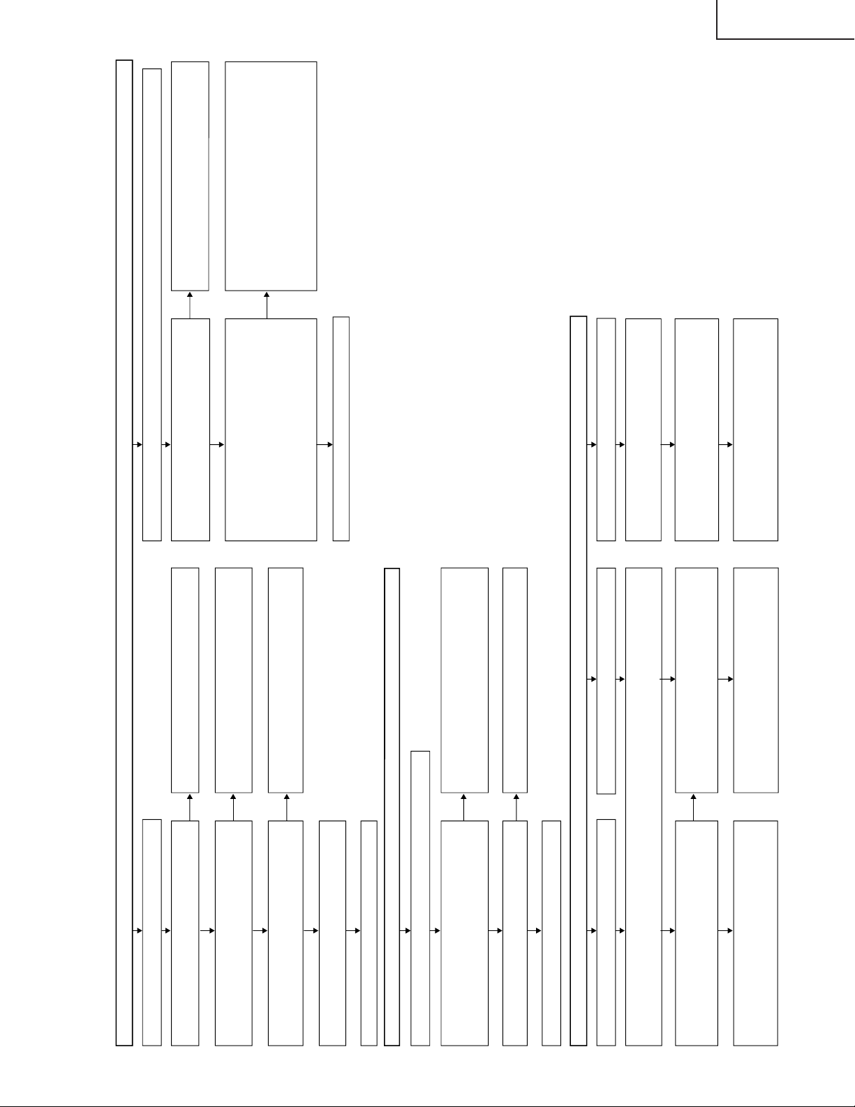
No sound (1)
No sound (2)
AVC System
No sound (3)
No sound is heard from the speaker in all modes.
Check audio circuits of the Display.
Is the monitor audio output set to "Variable"? Or
Is the headphone connected?
Are the audio outputs of IC2501 (multi-sound
processor) in order?
Pins 36 and 37 of IC2501 (SC1 OUT L/R).
Check IC2501 (multi-sound processor) and its
peripheral circuits.
Check lines and devices between pins 36/37 of
IC2501 and pins 1/3 of the AV unit connector
(P2502). (Q2504-5, Q2509-10 and Q2513-4)
Set the monitor audio output to "Fixed".
Remove the headphone.
The speaker generates no sound when audio signals are inputted from an external device or a PC.
Check IC1301 (A switch) and its peripherals.
Are the audio outputs of IC1301 (AV switch) in
order?
Pins 52 and 54 of IC1301 (TV MAIN OUT L/R)
Are the audio inputs of IC1301 (AV switch) in
order?
Input 1: Between pins 2 and 4 of IC1301
Input 2: Between pins 9 and 11 of IC1301
Input 3: Between pins 16 and 18 of IC1301
Input 4: Between pins 23 and 25 of IC1301
PC input: Between pins 29 and 31 of IC1301
Are the audio input circuits of IC1301 (AV switch)
in order?
Input 1: Between pins 6/2 and pins 2/4 of IC1301
Input 2: Between pins 6/2 and pins 9/11 of IC1301
Input 3:
Between pins 6/2 and pins 16/18 of IC1301
Front panel input: Between J2404 and pins 23/25
of IC1301
PC input: Between J2403 and pins 29/31 of IC1301
Are the audio inputs of IC2501 (multi-sound
processor) in order?
Pins 56 and 57 of IC2501 (SCI IN1 L/R)
YES
NO
YES
YES
YES
NO
NO
NO
No audio output <Input1> No audio output <INPUT2/3>
Has the input mode been selected on the Input Select screen?
Are the audio outputs of IC2501 (multi-sound
processor) in order?
Pins 27 and 28 of IC2501 (DRCM L/R)
Check lines and devices between pins 27/28 of
IC2501 and pins 3/1 of INPUT1. Also check the
audio mute circuits.
(IC2504, Q1101-2)
Are the audio outputs of IC1301 (AV switch) in
order?
Pins 43 and 45 of IC1301 (SC1 TV SUB OUT L/R)
Check lines and devices between pins 43/45 of
IC1301 and pins 3/1 of INPUT2/3. Also check
the audio mute circuits.
(IC1301, Q1104-7 and Q1109-12)
No monitor audio output or abnormal audio
The audio level is abnormal:
Is the monitor audio output set correctly?
"Variable" or "Fixed"
NO
YES
No sound at all:
Are the audio outputs of IC2501 (Multi-sound
processor) in order?
Pins 34 and 33 (SC2 OUT L/R) of IC2501
Check lines and devices between pins 34/33 of
IC2501 and the monitor output (J1101). Also
check the audio mute circuit.
(Q2502-3, Q1114-5 and Q1106-7)
YES
Check peripherals of the SR unit DISPLAY
OUTPUT 2 pin (SC6000).
YES
YES
YES
YES
YES
Are audio signals applied to the AV unit
connectors (pins 1 and 3 of P2502)?
YES
The speaker generates no sound when TV signal is received.
Are the tuner audio inputs of IC2501 (multi-sound
processor) in order?
Pin 67 (sound IF1) of IC2501
Pin 69 (sound IF2) of IC2501
Is the audio signal applied to tuner output pin 21?
Check B.P.F. of SIF1 and SIF2.
(Q1119-20 and Q1121-2)
Check IC2501 (multi-sound processor) and its
peripheral circuits.
YES
YES
NO
NO
Check TU1101 (U/V tuner) and its peripherals.
LC-30HV4E
53
Page 54

LC-30HV4E
No image (1)
AVC System
YES
NO
No video image on INPUT1
Has "INPUT1" been selected on the Input
Select screen?
Select INPUT1 CVBS on the Input Select
screen.
YES
NO
Is the video signal applied to pin 1 of IC1301
(AV switch)?
Check lines and devices between pin 20 of
INPUT1 (SC1101) and pin 1 of IC1301.
YES
NO
Select INPUT2 CVBS on the Input Select
screen.
YES
YES
(A) (B)
YES
NO
Is the video signal applied to pin 8 of IC1301
(AV switch)?
Check lines and devices between pin 20 of
INPUT2 (SC1102 1/2) and pin 8 of IC1301.
NO video image on INPUT2
Has "INPUT2" been selected on the Input
Select screen?
<When video signal is received>
No image (2)
YES
NO
NO video image on INPUT3
Has "INPUT3" been selected on the Input
Select screen?
Select INPUT3 CVBS on the Input Select
screen.
YES
NO
Is the video signal applied to pin 1 of IC1301
(AV switch)?
Check lines and devices between pin 20 of
INPUT3 (SC1102 1/2) and pin 15 of IC1301.
YES
NO
Select INPUT4 CVBS on the Input Select
screen.
YES
YES
(C) (D)
YES
NO
Is the video signal applied to pin 22 of
IC1301 (AV switch)?
Check lines and devices between pin 3 of
INPUT4 (J2404) and pin 22 of IC1301.
NO video image on INPUT4
Has "INPUT4" been selected on the Input
Select screen?
<When video signal is received>
No image (3)
YES
NO
No Y/C image on INPUT2
Has "INPUT2" been selected on the Input
Select screen?
Select INPUT2 Y/C on the Input Select
screen.
YES
NO
Is the Y/C signal applied to pins 10 and 12
of IC1301 (AV switch)?
Check lines and devices between pins20/15 of
INPUT1 (SC1101) and pins 10/12 of IC1301.
YES
NO
Select INPUT3 Y/C on the Input Select
screen.
YES
YES
(E) (F)
YES
NO
Is the Y/C signal applied to pins 17 and 19
of IC1301 (AV switch)?
Check lines and devices between pins20/15
of INPUT2 (SC1102 1/2) and pins 17/19 of
IC1301.
No Y/C image on INPUT3
Has "INPUT3" been selected on the Input
Select screen?
<When Y/C signal is received>
No image (4)
YES
NO
No Y/C image on INPUT4
Has "INPUT4" been selected on the Input
Select screen?
Select INPUT4 Y/C on the Input Select
screen.
YES
NO
Is the Y/C signal applied to pins 24 and 262
of IC1301 (AV switch)?
Check lines and devices between pins3/4 of
INPUT1 (J2401) and pins 24/26 of IC1301.
YES
(G)
<When Y/C signal is received>
54
Page 55
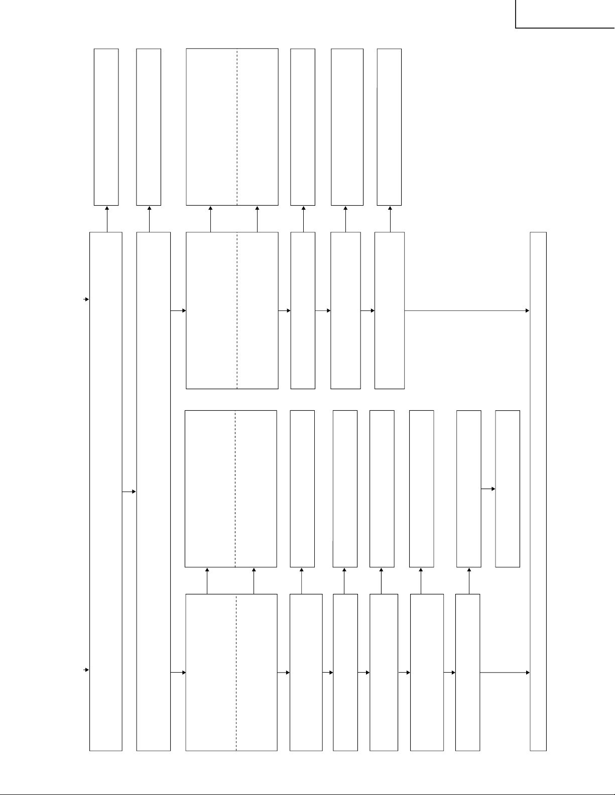
(A),(C),(E),(G) (B),(D),(F)
<When video signal is received> Are the main video signal and sub video signal sent from pin 56 and pin 44 of IC1301 respective
ly?
<When Y/C signal is received> Are the main Y signal, main C signal, sub Y signal and sub C signal sent from pin 56, pin 58, pin
44 and pin 47 of
IC1301 respectively?
Check IC1301 (AV switch) and its peripheral
circuits.
<When video signal is received> Is the video signal applied to pin 7 of IC401 (main comb filter) and pin 7 of IC402 (sub comb f
ilter)?
<When Y/C signal is received> Are the main signal and sub signal applied to pins 44 and 43 of IC801 (main video chroma) and pin
s 5 and 7 of IC802
(sub video chroma) respectively?
Check lines and devices between IC1301
and IC401/IC402/IC801/IC802.
<Main system>
YES
YES
YES
YES
YES
YES
YES
YES
YES
YES
YES
YES
YES
NO
NO
NO
NO
NO
NO
NO
NO
NO
NO
NO
NO
NO
<When video signal is received>
Are the main Y signal and main C signal
applied to pin 1 (TP812) and pin 48 of
IC801 (main video chroma) respectively?
<When video signal is received>
Check lines and devices between IC4001
and IC801.
(IC403, Q415, etc.)
<When Y/C signal is received>
Are the main Y signal and main C signal
applied to pin 44 and pin 43 of IC801 (main
video chroma) respectively?
<When Y/C signal is received>
Check lines and devices between IC1301
and IC801.
(Q827, Q403, Q404, etc.)
Are the main Y, Cb and Cr signals sent
from pins 21, 22 and 23 of IC801
Check IC801 (main video chroma) and its
peripheral circuits.
Are the main Y, Cb and Cr signals applied to
pins 69, 68 and 67 of IC803 (RGB decoder)
Check lines and devices between IC801
and IC803. (IC814, Q814, Q815, etc.)
Are the main R, G and B signals sent from
pins 35, 37 and 39 of IC803 respectively?
Check IC803 (RGB decoder) and its
peripheral circuits.
Are the main R, G and B signals applied to
pins 3, 7 and 10 of FL810 (6.7/30 MHz
L.P.F.) respectively?
Are the main R, G and B signals sent from
pins 19, 15 and 12 of FL810 respectively?
Check lines and devices between IC803
and FL810.(Q801-3 etc.)
Is cutoff frequency setting pin 17 of FL810
(6.7/30 MHz L.P.F.) pulled high?
Check FL810 (6.7/30 MHz L.P.F.) and its
peripheral circuits.
Check the PC I/F unit.
<Sub system>
<When video signal is received>
Are the sub Y signal and sub C signal
applied to pin 1 and pin 7 of IC802 (sub
video chroma) respectively?
<When video signal is received>
Check lines and devices between IC402
and IC802.
(IC404, Q416-8, etc.)
<When Y/C signal is received>
Are the sub Y signal and sub C signal
applied to pin 5 and pin 7 of IC802 (sub
video chroma) respectively?
<When Y/C signal is received>
Check lines and devices between IC1301
and IC802.
(IC828, Q409, Q410, etc.)
Are the sub Y, Cb and Cr signals sent from
pins 21, 22 and 23 of IC802 respectively?
Check IC802 (sub video chroma) and its
peripheral circuits.
Are the sub Y, Cb and Cr signals applied to
Q901-2, Q903-4 and Q905-6 (6.7 MHz
L.P.F.) respectively?
Check lines and devices between IC802
and Q901-2/Q903-4/Q 905-6 (6.7 MHz
L.P.F.).
Are the sub R, G and B signals sent from
Q901-2, Q903-4 and Q905-6 (6.7 MHz
L.P.F.) respectively?
Check peripherals of Q901-2, Q903-4 and
Q905-6 (6.7 MHz L.P.F.).
LC-30HV4E
55
Page 56

LC-30HV4E
Check the PC I/F unit.
AVC System
<When component/RGB signal is received> No image (5)
No RGB image on INPUT1
Has "INPUT1" been selected
on the Input Select screen?
Are RGB signals applied to
pins 63, 59 and 61 of IC1401
(AV switch)?
Select INPUT1 RGB on
the Input Select screen.
Check lines and devices
between pins 15/11/7 of
INPUT1 (SC1101) and
pins 63/59/61 of IC1301.
No RGB image on INPUT3
Has "INPUT3" been selected
on the Input Select screen?
NO
NO
YES
NO
NO
NO
NO
NO
YES
YES
YES
YES
YES
YES
YES
YES
YES
YES
NO
NO
NO
YES
YES
NO
NO
NO
NO
NO
NO
NO
YES
YES
YES
YES
YES
YES
Select INPUT3 RGB on the
Input Select screen.
Are RGB signals applied to
pins 9, 5 and 7 of IC1401
(AV switch)?
Check lines and devices
between pins 15/11/7 of
INPUT3 (SC1102) and pins
9/5/7 of IC1301.
No component image on INPUT3
Has "INPUT3" been
selected on the Input Select
screen?
Select INPUT3
COMPONENT on the Input
Select screen.
Are RGB signals applied to
pins 5, 17 and 19 of
IC1401 (AV switch)?
Check lines and devices
between pins 8/26/17 of
INPUT3 (J1101) and pins
15/17/19 of IC1301.
Are the main video signal, pass signal and sub video signal sent from pins 34, 38 and 36 of IC1401 respectively?
Are Y, Cb and Cr signals applied
to pins 19, 18 and 17 of IC801
(main video chroma) respectively?
<Main 525i system>
<Pass 525P/1125i/750P system>
Check lines and devices between
pins 46/50/48 of IC1401 and pins
19/18/17 of IC801.
Are the main Y, Cb and Cr
signals sent from pins 21, 22
and 23 of IC801 respectively?
Check IB801 (main video
chroma) and its peripheral
circuits.
Are the main Y, Cb and Cr
signals applied to pins 69, 68
and 67 of IC803 respectively?
Check lines and devices
between IC801 and IC803.
(IC814, Q814-5, etc.)
Are Y, Cb and Cr signals applied
to pins 5, 4 and 3 of IC803
(RGB decoder) respectively?
Check lines and devices
between pins34/38/36 of
IC1401 and pins 5/4/3 of IC803.
Are the main R, G and Br
signals sent from pins 35, 37
and 39 of IC803 respectively?
Check IC803 (RGB decoder)
and its peripheral circuits.
Are the main R, G and Br
signals applied to pins 3, 7 and
10 of IC810 (6.7/30 MHz L.P.F.)
respectively?
Check lines and devices
between IC803 and FL810.
(Q801-3 etc.)
Are the main R, G and Br
signals sent from pins 19, 15
and 12 of IC810 respectively?
The cutoff frequency of FL810
(L.P.F.) is switched as follows
depending on the input
signals:
Status of pin 17 for setting the
cutoff frequency of FL810 (6.7/30
MHz L.P.F.)
<525i system>: High
<525P/1125i/750P system>: Low
Check FL810 (6.7/30 MHZ L.P.F.)
and its peripheral circuits.
<Sub system>
Are Y, Cb and Cr signals
applied to pins 19, 18 and 17
of IC802 (sub video chroma)
respectively?
Check IC1401 (AV switch)
and its peripheral circuits.
Check lines and devices
between pins 40/44/42 of IC
1401 and pins 19/18/17 of
IC802.
Are the sub Y, Cb and Cr
signals sent from pins 21, 22
and 23 of IC802 respectively?
Check IC802 (sub video chroma)
and its peripheral circuits.
Are the sub Y, Cb and Cr signals
applied to Q901-2, Q903-4 and
Q905-6 (6.7 MHz L.P.F.)
respectively?
Check lines and devices between
IC802 and Q901-2/Q903-4/Q905-
6 (6.7 MHz L.P.F.).
Are the sub R, G and B signals
sent from Q901-2, Q903-4 and
Q905-6 (6.7 MHz L.P.F.)
respectively?
Check peripherals of Q901-
2/Q903-4/Q905-6 (6.7 MHz
L.P.F.).
56
Page 57
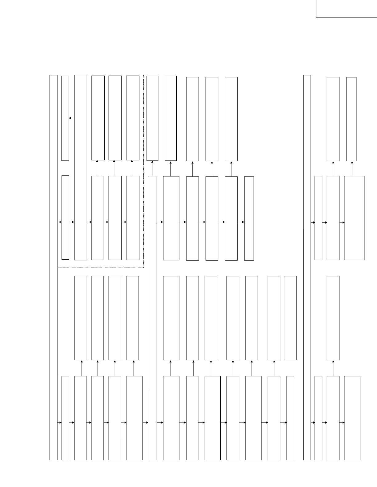
LC-30HV4E
No image (6)
AVC System
No image when TV signal is received
Check the PC I/F unit.
No teletext screen appears.
Is the video signal on tuner image output
pin 23?
Check peripherals of the tuner (TU1101)
and replace if necessary.
Is the video signal on pin 5 of IC1106 (level
adj.) or TP1101?
Is the video signal applied to pin 63 of
IC1301 (AV switch)?
Is the level control signal sent from pin 1 of
IC1108 to pin 8 of IC1103 (AV switch)?
YES
No Monitor image <AV-OUT>
YES
NO
NO
NO
NO
NO
NO
NO
NO
NO
NO
NO
YES
YES
YES
YES
YES
YES
YES
YES
YES
YES
YES
Check lines and devices between pin 5 of
IC1106 and pin 63 of IC1301.
Are the main video signal and sub video
signal sent from pin 30 of IC1301 and pin
44 of IC1301 respectively?
Check IC1301 (AV switch) and its
peripheral circuits.
Is the teletext signal received (is a teletext-supporting receiver connected to the video input
terminal) and TELETEXT selected on the remote controller?
Select TELETEXT in an appropriate manner.
Is the video signal applied to pin 21 of
IC1601 (teletext CPU)?
Check lines and devices between pin 56 of
IC1301 (AV switch) and pin 21 of IC1601.
Is the text signal sent from pins 57, 58 and
59 of IC1601?
Check IC1601 and its peripheral circuits.
Is the text signal applied to pins 57, 53 and
55 of IC1401 (AV switch)?
Check lines and devices between pins 57/58/59
of IC1601 and pins 57/53/55 of IC1301.
NO
YES
NO
NO
NO
NO
YES
YES
YES
YES
Is the video signal applied to pin 7 of IC401 (main comb filter) and pin 7 of IC402 (sub comb filter)?
<Main system>
Are the main Y and C signals applied to
pin 1 (TP812) and pin 48 of IC801 (main
video chroma) respectively?
Check lines and devices between IC4001
and IC801.
(IC403, Q415, etc.)
Are the main Y, Cb and Cr signals sent from pins
21, 22 and 23 of IC801 respectively?
Check IC801 (main video chroma) and its
peripheral circuits.
Are the main Y, Cb and Cr signals applied to pins
69, 68 and 67 of IC803 (RGB decoder)
respectively?
Check lines and devices between IC801 and
IC803. (IC814, Q814, Q815, etc.)
Are the main R, G and B signals sent from
pins 35, 37 and 39 of IC803 respectively?
Check IC803 (RGB decoder) and its
peripheral circuits.
Are the main R, G and B signals sent from
pins 19, 15 and 12 of FL810 respectively?
Is cutoff frequency setting pin 17 of FL810
(6.7/30 MHz L.P.F.) pulled high?
Is the video signal sent from pin 4 of
IC1301 (AV switch)?
YES
Check lines and devices between pin 41 of
IC1301 and monitor image output pin 20 (J1101).
(Q1403 and Q1113)
Check IC1301 and its peripheral circuits.
No monitor image <S-OUT>
YES
NO
NO
Are Y and C signals sent from pins 39 and
37 of IC1301 (AV switch) respectively?
YES
Check lines and devices between pins
39/37 of IC1301 and monitor S-OUT pins
3/4 (SC1102).
(Q1401-2)
Check that input signal is S-INPUT.
Check FL810 (6.7/30 MHz L.P.F.) and its
peripheral circuits.
Are the main R, G and B signals applied to
pins 3, 7 and 10 of FL810 (6.7/30 MHz
L.P.F.) respectively?
Check lines and devices between IC803
and FL810.(Q801-3 etc.)
Check lines and devices between IC1301
and IC401/402.
NO
NO
Check lines and devices between IC402
and IC802. (IC404, Q416-8, etc.)
Are the sub Y and C signals applied to pin
1 (TP813) and pin 48 (TP407) of IC802
(sub video chroma) respectively?
Are the sub Y, Cb and Cr signals sent from
pins 21, 22 and 23 of IC802 respectively?
Check IC802 (sub video chroma) and its
peripheral circuits.
YES
NO
Are the sub Y, Cb and Cr signals applied to Q901-2,
Q903-4 and Q905-6 (6.7 MHz L.P.F.) respectively?
Check lines and devices between IC802 and
Q901-2/Q903-4/Q905-6 (6.7 MHz L.P.F.).
YES
NO
Are the sub R, G and B signals sent from Q901-2,
Q903-4 and Q905-6 (6.7 MHz L.P.F.) respectively?
YES
Check the PC I/F unit.
Check Q901-2, Q903-4 and Q905-6 (6.7
MHz L.P.F.) and their peripheral circuits.
<Sub system>
No image (7)
Check IC1301 and its peripheral circuits
57
Page 58

LC-30HV4E
NO
YES
Is HD1/VD1 outputted to pins
(9) and (4) of IC801,
respectively?
Check IC801 and its peripheral
circuits.
NO
YES
Is HD2/VD2 outputted
to pins (9) and (4) of
IC802, respectively?
Check IC802 and its
peripheral circuits.
NO
YES
Is HD1/VD1 outputted to pins
(44) and (2) of IC1901,
respectively?
Check the circuit between pins
(9)/(4) of IC801 and pins
(44)/(2) of IC1901.
NO
YES
Is HD2/VD2 inputted to
pins (19) and (20) of
IC1901, respectively?
Check the circuit
between pins (9)/(4) of
IC1901 and pins
NO
YES
Check IC1901 and its
peripheral circuits.
NO
YES
Is HDS/VDS inputted to
pins (21) and (22) of
IC1901, respectively?
Check IC1901 and its
peripheral circuits.
NO
YES
Is HD3/VD3 inputted to pins
(14) and (13) of IC604,
respectively?
Check the circuit between pins
(8)/(10) of IC1901 and pins
(14)/(13) of IC604.
NO
YES
Is SP-HD/SP-VD/SP-CP
outputted to pins (16) , (28) and
(15) of IC604, respectively?
Check IC604 and its peripheral
circuits.
NO
YES
Is SP-HD/SP-VD/SP-CP
inputted to pins (40) , (5) and
(6) of IC1901, respectively?
Check the circuit between pins
(16)/(28)/(15) of IC604 and pins
(40)/(5)/(6) of IC1901.
NO
YES
Is PL-HD/PL-VD/PL-CP/PL-HBLK
outputted to pins (34) , (35), (33)
and (31) of IC1901, respectively?
Check IC1901 and its
peripheral circuits.
NO
YES
Is Hsync/Vsync/SCP inputted
to pins (1) , (2) and (31) of
IC803, respectively?
Check the circuit between pins
(34)/(35)/(33)/(31) of IC1901
and pins (1)/(2)/(31) of IC803.
NO
YES
Is HS/VS outputted to pins
(29) and (28) of IC803,
respectively?
Check IC803 and its peripheral
circuits.
Check PC I/F Unit.
Is HD3/VD3 outputted to pins
(8) and (10) of IC1901,
respectively?
NO
YES
Is HD_50/VD_50 outputted to
pins (79) and (80) of IC803,
respectively?
Check IC803 and its peripheral
circuits.
NO
YES
Is HD_50/VD_50 inputted to
pins (3) and (4) of IC803,
respectively?
Check the circuit between pins
(79)/(80) of IC803 and pins
(3)/(4) of IC604.
NO
YES
YES
Check IC604 and its
peripheral circuits.
NO
Is SP-HD/SP-VD outputted to
pins (40) and (5) of IC1901,
respectively?
Check the circuit between pins
(16)/(28) of IC604 and pins
(40)/(5) of IC1901.
Is SP-HD/SP-VD outputted to
pins (16) and (28) of IC604,
respectively?
<MAIN system; 15k> <MAIN system; 1080i/625P>
<SUB system>
<MAIN system; D2/D3/D4>
Synchronization failure
TROUBLE SHOOTING TABLE (Continued)
(AVC System)
58
Page 59

NO
YES
No TV, video and component picture
Is input at pins (124),
(133) and (139) of IC4
normal?
Check CN6 and its
peripheral circuits.
NO
YES
Are TL207, TL208 and
TL211 normal?
Check CN6 and its
peripheral circuits.
NO
YES
Is digital output section of
IC4 normal?
Check IC4 and its
peripheral circuits.
NO
YES
Is digital output section
of IC310 normal?
Check IC310 and its
peripheral circuits.
NO
YES
Is digital output of IC25
normal?
Check IC25 and its
peripheral circuits.
No PC picture
YES
Is signal at pins (21), (22), (24), (25), (27), (28), (30) and (31)
of IC413? (The signal is of high frequency (a little less than
1GHz). Pay due attention to it during observation.)
Connecting cable or
monitor is problem.
NO
PC I/F Unit (CPCi-
0056CE) internal problem
is likely.
No MAIN picture on single screen and dual screen.
No SUB picture on dual screen
NO
YES
Is input at pins (126),
(136) and (141) of IC4
normal?
Check CN8 and its
peripheral circuits.
NO
YES
Is digital output section
of IC4 normal?
Check IC4 and its
peripheral circuits.
NO
YES
Is digital output of IC25
normal?
Check IC25 and its
peripheral circuits.
No picture
TROUBLE SHOOTING TABLE OF PC I/F UNIT
(AVC System)
LC-30HV4E
59
Page 60
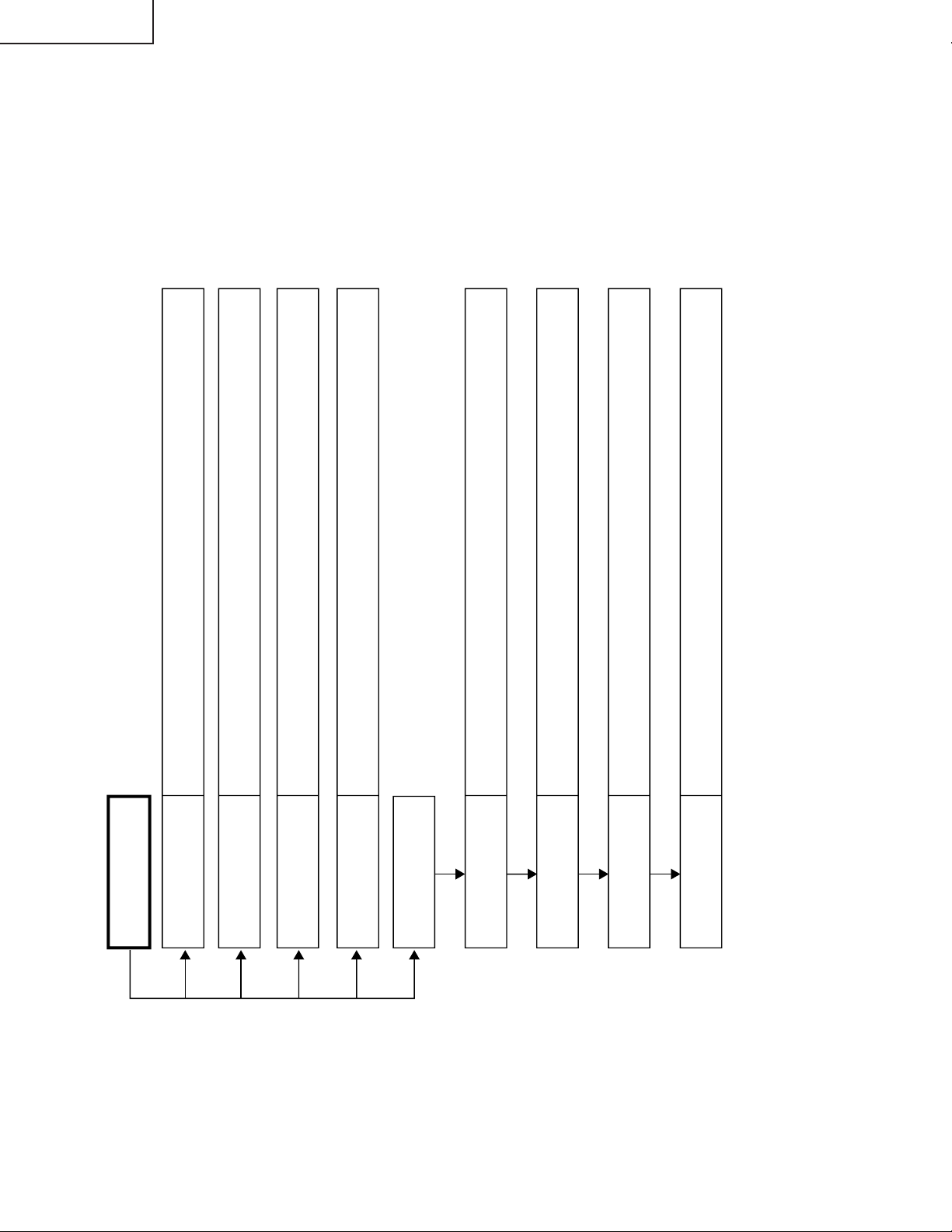
LC-30HV4E
LCD LED: ON
AVC-C LED: OFF
Check power switch, AC power cable and power unit of AVC-C.
LCD LED: OFF
AVC-C LED: ON
Check power switch, AC power cable and power unit of LCD.
LCD LED: BLINKING
(Once per second)
Check system cable, power switch, AC power cable and power unit of AVC-C.
LCD LED: BLINKING
(4 times per second)
Check cooling fan, IC2102 and peripheral circuits.
LCD LED: ON IN RED
AVC-C LED: ON IN RED
LCD LED never turns to
green.
Check power switch, AC power cable and power unit of LCD.
AVC-C LED never turns
to green.
Check power switch, AC power cable and power unit of AVC-C.
LCD panel backlight
never lights up.
Reset the lamp error count. (See adjustment procedure.)
Check Q6551, Q6554, Q6557, Q6560, Q6563, and Q6566 as well as peripheral circuits.
Initialize EEPROM. (See
adjustment procedure.)
If not successful: Check power switch, AC power cable and power unit of LCD.
No Power
TROUBLE SHOOTING TABLE
(Display)
60
Page 61

TROUBLE SHOOTING TABLE (Continued)
No 800-MHz signal input at pins (186), (187), (191), (192), (196) and (197) of IC2201.
Check system cable and connector.
No signal output from pins (95), (96) and (97) of IC2201.
Check IC2201 and peripheral circuits.
Disconnect system cable and operate LCD independently. (Blue screen appears.)
Check system cable, connector and peripheral circuits.
Is each pin normal at IC4701?
Faulty: Check IC4701 and peripheral circuits.
Is each pin normal at IC4901?
Faulty: Check IC4901 and peripheral circuits.
Is each pin normal at IC4551?
Faulty: Check IC4551 and peripheral circuits.
Check SC4501, -4502, -4503 and -4504 and their cables.
Check outputs of main unit and headphone.
Is signal waveform normal at Q2105 and Q2106?
Faulty: Check Q2105 and Q2106 and peripheral circuits.
Is signal waveform normal at IC3802 and IC3804?
Faulty: Check IC3802 and IC3804 and peripheral circuits.
Is signal waveform normal at IC3805, IC3806 and IC3807?
Faulty: Check IC3805, IC3806 and IC3807 and peripheral circuits.
Check IC3809 and peripheral circuits.
1No Picture
2No Sound
(Display)
LC-30HV4E
61
Page 62

CHASSIS LAYOUT (AVC System)
H
G
F
LC-30HV4E
E
D
C
B
A
121110987654321
62
63
Page 63

CHASSIS LAYOUT (Display)
H
G
F
LC-30HV4E
E
D
C
B
A
121110987654321
64
65
Page 64

SYSTEM BLOCK DIAGRAM (AVC System)
H
G
F
LC-30HV4E
E
D
C
B
A
121110987654321
66
67
Page 65
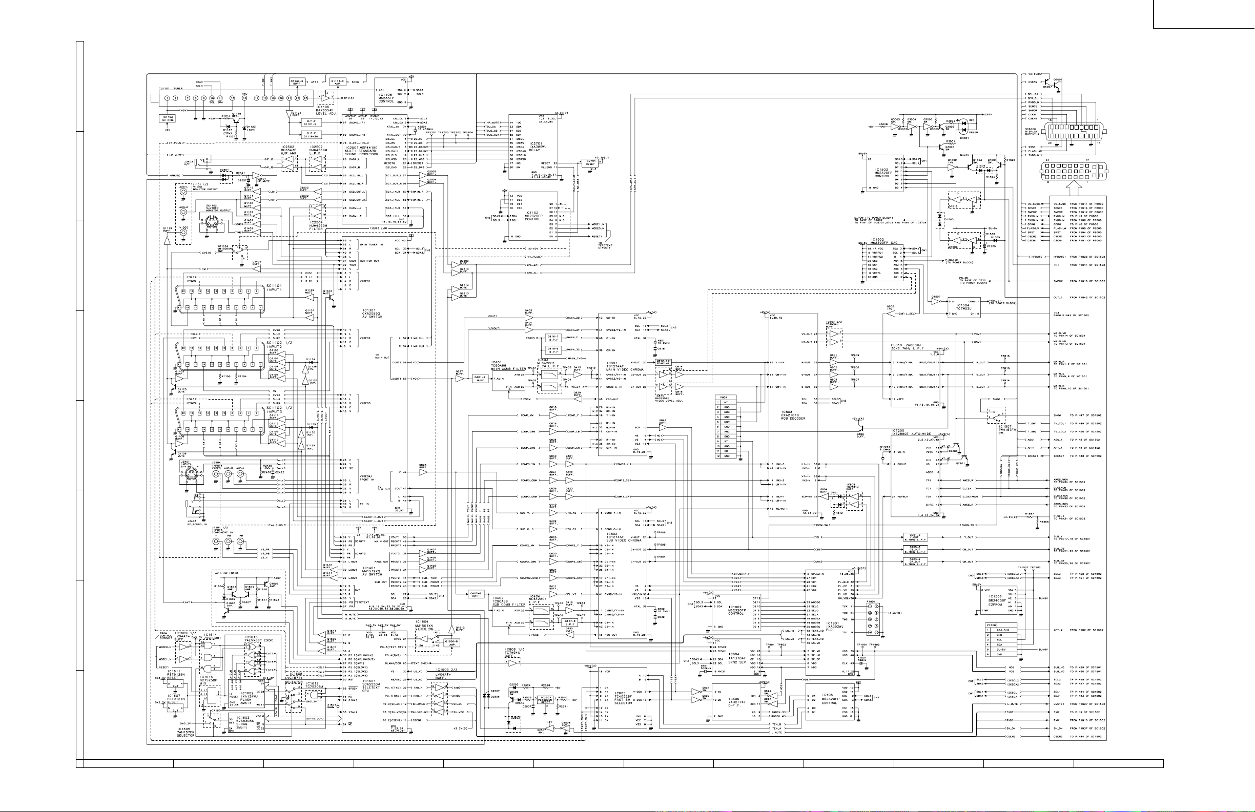
SIGNAL FLOW BLOCK DIAGRAM (AVC System)
H
G
F
LC-30HV4E
E
D
C
B
A
121110987654321
68
69
Page 66

POWER SYSTEM BLOCK DIAGRAM (AVC System)
H
G
F
LC-30HV4E
E
D
C
B
A
121110987654321
70
71
Page 67

PC I/F UNIT BLOCK DIAGRAM (AVC System)
H
G
F
LC-30HV4E
E
D
C
B
A
121110987654321
72
73
Page 68

SIGNAL BLOCK DIAGRAM (Display)
H
TMDS
G
F
SC2201
DISPLAY
INPUT 1
DDC 5V
DDC-IIC
IC2202
HDCP( KEY)
EEP-ROM
KEY IIC
TMDS RECEIVER
IC2204
DDC
EEP-ROM
IC2201
QO 0-23 ,QE0- 23
HSYNC,V SYNC
CLOCK
IC2203
CONFIG
EEP-ROM
CO N FI G IIC
IC4902
FIFO M EMORY
IC4901
OS DRIVE (ODD)
IC4702
FIFO M EMORY
IC4701
O S D RIV E( EV EN)
LC-30HV4E
LCD
PANEL
IC2002
RESET
E
CONTROL
SC2202
DISPLAY
INPUT 2
D
C
J201
SPEAKER(L)
B
PLUG
AUDIO
CONTROL KEY
IC3802
SRS FORC US
AUDIO PR OC ESSO R
IC3804
SOUND CONTROL
IC2001
MICRO PROCESSOR
IC2003
EEP-ROM
R/C RECEIVER
OPC
LED
IC3803
EX TE NTION
DAC
IC4551
LCD CONTROL
OFL
INVER TER
INVER TER
Q6551
Q6554
Q6557
DC/AC
DRIVE
Q6560
Q6563
Q6566
DC/AC
DRIVE
T6551
T6552
T6553
T6554
T6555
T6556
DC/AC
TRANS
BACK LIGHT
T6557
T6558
T6559
T6560
T6551
T6562
DC/AC
TRANS
J202
SPEAKER(R)
PLUG
A
J3801
HEAD PHONES
JA CK
74
IC3809
S-OUT AMP
IC3810
HEAD-PHONE
AMP
121110987654321
75
Page 69

POWER UNIT BLOCK DIAGRAM (Display)
LC-30HV4E
OPERATION
H
G
F
INVERTER GND
E
SW136
AC SW
P131
AA
+5V
LCD_CONTROL(DIGITAL)
IC4112
3.3V REG
VSH+3.3V
FAN
IC4559
IC4560
13V REG
VLS+13V
MAIN
(TMDS/MICOM)
P2103
MB
IC4558
-6VREG
VEE-6V
+9V
FAN VCC
IC2102
9VREG
IC4556
5VREG
DAC+5V
D4555
SIN+4V
IC4557
6VREG
IC4555
34V REG
VBH+34V
POWER
P4101
PC
CN5
PC
+13V
@
IC4516
3.3V REG
IC4515
2.5V REG
13V IC13V PANEL
B+3.3VCONT
B+2.5VCONT
INVERTER1
INV.VCC
P6557
PG
INVERTER2
P6564
PH
INV.VCC
P2106
MD
+5V
P2104
SA
P2003
RM
+2. 5V
+3. 3V
+5V _STB
IC2105
2.5V REG
IC2104
3.3V REG
IC2101
5VREG
+13V
P2101
PB
P2101
PA
STB+6V
CN4
PB
CN3
PA
CN2
AA
+10V
+13V
STB+6V
CN1
AC IN
CN7
PE
P6907
MD
D
C
B
AUDIO
IC2103
5VREG
+13V
IC3801
9VREG
+5V
P3801
SA
+9V
76
R/C.LED
+5V _STB
P101
RM
121110987654321
77
A
Page 70

O VERALL WIRING DIAGRAM-1/2 (AVC system)
H
G
F
LC-30HV4E
E
D
C
B
A
121110987654321
78
79
Page 71

O VERALL WIRING DIAGRAM-2/2 (AVC system)
H
G
F
LC-30HV4E
E
D
C
B
A
121110987654321
80
81
Page 72

OVERALL WIRING DIAGRAM (Display)
H
G
F
LC-30HV4E
E
D
C
B
A
121110987654321
82
83
Page 73

LC-30HV4E
DESCRIPTION OF SCHEMATIC DIAGRAM
VOLTAGE MEASUREMENT CONDITION:
1. When the exclusive-use AC adapter is used, the colour
bar signal of colour bar generator for service is input to
get the normal screen. When the audio is minimized,
the voltage value is measured with the 20 kΩ/V tester.
WAVEFORM MEASUREMENT CONDITION:
1. When the exclusive-use AC adapter is used, the colour
density, lightness and colour hue are set to the center
position, and the signal of colour bar generator for
service is observed to get waveform.
2. indicates waveform check points (See chart,
wavefor ms are measured from point indicated to
chassis ground.)
INDICATION OF RESISTOR & CAPACITOR:
RESISTOR
1. The unit of resistance “Ω” is omitted.
(K=kΩ=1000 Ω, M=MΩ).
2. All resistors are ± 5%, unless otherwise noted.
(J= ± 5%, F= ± 1%, D= ± 0.5%)
3. All resistors are Carbon type, unless otherwise noted.
C : Solid W : Cement
S : Oxide Film T : Special
N : Metal Coating
CAPACITOR
1. All capacitors are mF, unless otherwise noted.
(P=pF=mmF).
2. All capacitors are Ceramic type, unless otherwise
noted.
(ML) : Mylar (TA) : Tantalum
(PF) : Polypro Film (ST) : Styrol
CAUTION:
This circuit diagram is original one, therefore there may be a
slight difference from yours.
IMPORTANT SAFETY NOTICE:
PARTS MARKED WITH
IMPORTANT FOR MAINTAINING THE SAFETY OF
THE SET. BE SURE TO REPLACE THESE PARTS
WITH SPECIFIED ONES FOR MAINTAINING THE
SAFETY AND PERFORMANCE OF THE SET.
“å”
( )ARE
84
Page 74

WAVEFORMS
LC-30HV4E
1
IC1301 63-pin
V: 200mV/div H: 10µsec/div
5
IC803 TP801
V: 200mV/div H: 20µsec/div
2
IC1301 56-pin
V: 500mV/div H: 10µsec/div
6
IC803 TP802
V: 200mV/div H: 20µsec/div
3
IC405 1.2-pin
V: 500mV/div H: 10µsec/div
7
IC803 TP803
V: 200mV/div H: 20µsec/div
4
IC801 1-pin
V: 200mV/div H: 10µsec/div
8
IC803 31-pin
V: 1V/div H: 20µsec/div
9
IC810 13-pin
V: 500mV/div H: 20µsec/div
0
IC810 11-pin
V: 500mV/div H: 20µsec/div
er
IC2201 96-pin
V: 1V/div H: 5msec/div
IC2201 97-pin
V: 1V/div H: 5µsec/div
q
IC810 10-pin
V: 500mV/div H: 20µsec/div
w
IC2201 95-pin
V: 1V/div H: 5µsec/div
85
Page 75

Ë MAIN Unit-1/6 (AVC System)
H
G
F
LC-30HV4E
E
D
C
B
A
121110987654321
86
87
Page 76

ËË
Ë MAIN Unit-2/6 (AVC System)
ËË
H
G
F
LC-30HV4E
E
D
C
B
A
121110987654321
88
89
Page 77
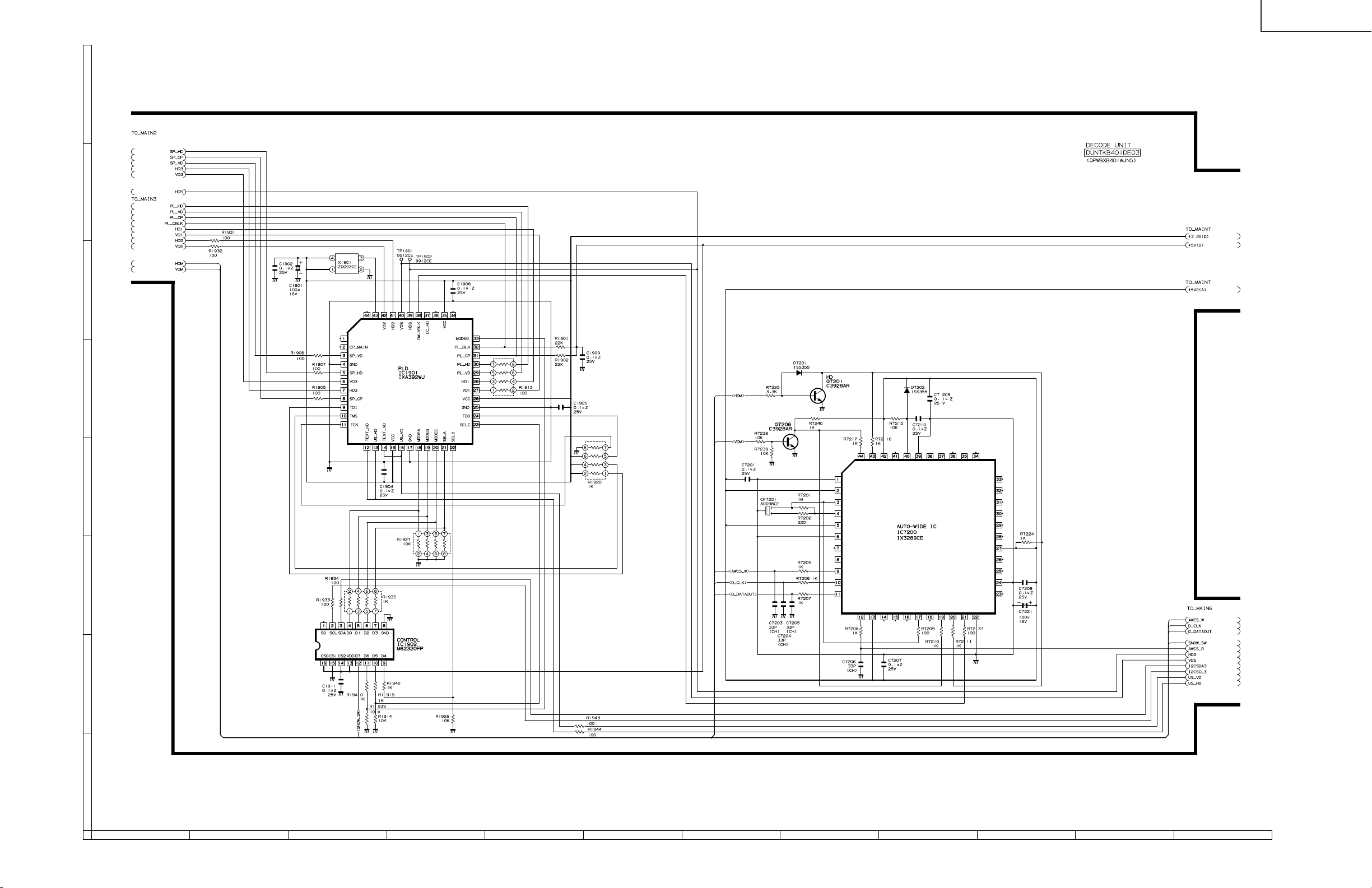
ËË
Ë MAIN Unit-3/6 (AVC System)
ËË
H
G
F
LC-30HV4E
E
D
C
B
A
121110987654321
90
91
Page 78
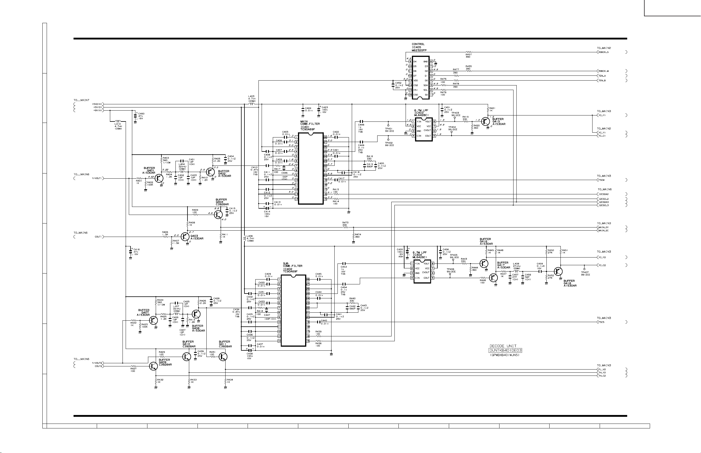
Ë MAIN Unit-4/6 (AVC System)
H
G
F
LC-30HV4E
E
D
C
B
A
121110987654321
92
93
Page 79
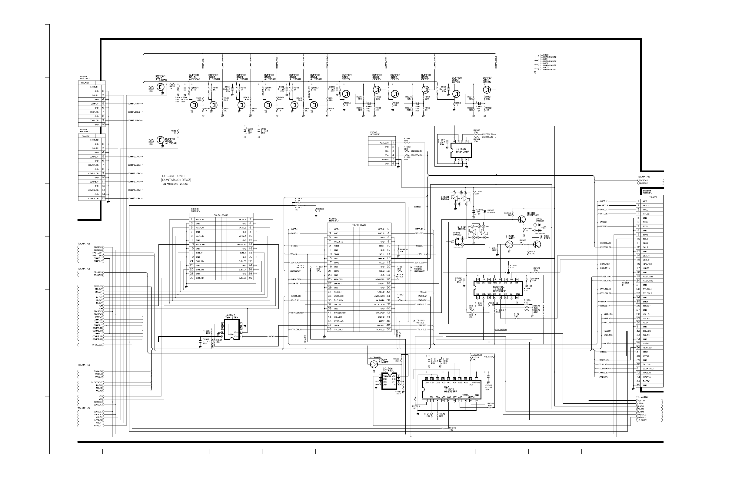
Ë MAIN Unit-5/6 (AVC System)
H
G
F
LC-30HV4E
E
D
C
B
A
121110987654321
94
95
Page 80

ËË
Ë MAIN Unit-6/6 (AVC System)
ËË
H
G
F
LC-30HV4E
E
D
C
B
A
121110987654321
96
97
Page 81

ËË
Ë FRONT Unit (AVC System)
ËË
H
G
F
LC-30HV4E
E
D
C
B
A
121110987654321
98
99
Page 82
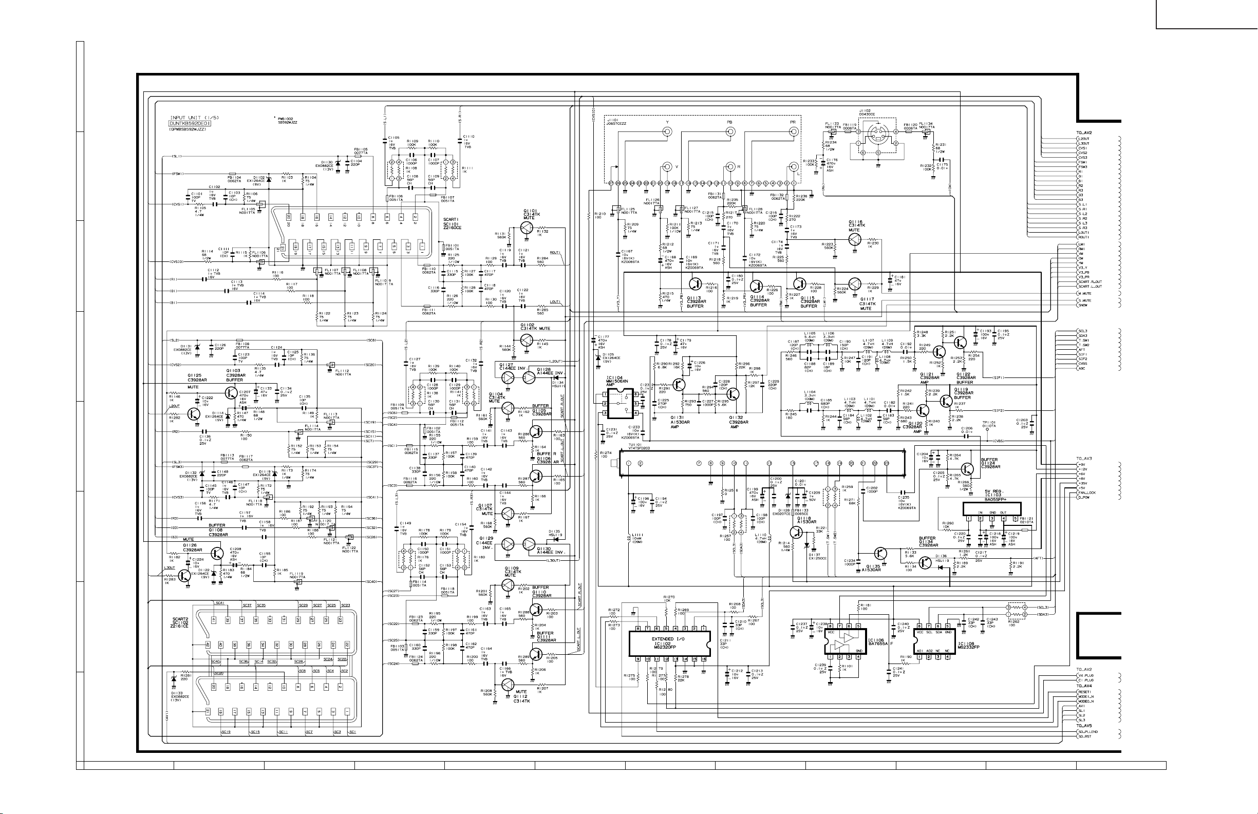
ËË
Ë AV Unit-1/5 (AVC System)
ËË
H
G
F
LC-30HV4E
E
D
C
B
A
121110987654321
100
101
Page 83

ËË
Ë AV Unit-2/5 (AVC System)
ËË
H
G
F
LC-30HV4E
E
D
C
B
A
121110987654321
102
103
Page 84

ËË
Ë AV Unit-3/5 (AVC System)
ËË
H
G
F
LC-30HV4E
E
D
C
B
A
121110987654321
104
105
Page 85

ËË
Ë AV Unit-4/5 (AVC System)
ËË
H
G
F
LC-30HV4E
E
D
C
B
A
121110987654321
106
107
Page 86

ËË
Ë AV Unit-5/5 (AVC System)
ËË
H
G
F
LC-30HV4E
E
D
C
B
A
121110987654321
108
109
Page 87

ËË
Ë SR Unit (AVC System)
ËË
H
G
F
LC-30HV4E
E
D
C
B
A
121110987654321
110
111
Page 88

ËË
Ë POWER Unit-1/2 (AVC System)
ËË
H
G
F
LC-30HV4E
E
D
C
B
A
121110987654321
112
113
Page 89

ËË
Ë POWER Unit-2/2 (AVC System)
ËË
H
G
F
LC-30HV4E
E
D
C
B
A
121110987654321
114
115
Page 90

Ë PC I/F Unit-1/7 (AVC System)
H
G
F
-C1_INT5
SSYSTEM3
CSEN1_SH3
DO_HDISP6,7
DO_VSYNC6,7
E
D
R16 560(1%)
1
VS
2
NC
3
TC
4 5
2.2K(1%)
R18
C30
0.047uF
GND RESET
IC19 PST623XW
C
IC2
PST600IM
Vcc
GND
OUT
B
A
SDA3I SCL3
SM_RST3
MON_DET7
HPMUTE13
LMUTE3
AWCS_R3
AWCS_W3
-RST_PL7
HVSEL4
VD+1.8
8
VCC
7
NC
6
NC
C31
0.1uF
VD+3.3
C33 0.1uF
1
2
3
+
IC3
1
A0
VCC
2
A1
TEST
3
NC
SCL
4 5
GND SDA
AT24C128N-10SI-2.7
VD+3.3
Q120
1
G1
2
S2
3 4
G2 D2
NDC7002N
C24
10uF/16V
C26
0.01uF
8
7
6
D1
S1
0.1uF
6
5
C32
VD+3.3
VD+3.3
LC-30HV4E
VD+3.3
166
167
SCK1
PTE7
165
TXD1
VSS
0.01uF
SCK0
CS0
C38
163
164
TXD0
VCC
-CS2
1
1
1
R877 10K
1.8432MH
C9 0.01uF
158
159
160
161
162
VSS
VCC
PTJ7
CKIO
PTH7
IRQOUT
CS2
CS3
CS4
CS5
CS6
CE2A
100
101
102
103
FLS_W 3
-WR/RD 2
TL98
TL99
-WEH 2,5
-WEL 2,5
-RD 2,5
TL100
157
PTJ6
EXTAL
XTAL
PTH6
CAP2
CAP1
PTF0
PTF1
PTF2
PTF3
PTF4
PTF5
PTF6
PTF7
PTG0
PTG1
PTG2
PTG3
PTG4
PTG5
PTG6
PTG7
PTH5
RESETM
WAIT
BREQ
BACK
PTE0
PTE1
PTE2
PTE3
PTE6
DACK1
DACK0
PTJ5
PTJ4
CASLH
CASLL
RAS2L
RAS3L
CE2B
104
VCC
VSS
VSS
VCC
VSS
VSS
VCC
MD0
VCC
VSS
VCC
VSS
CKE
1
2
1
2
D50
MA157A
AGC_13
AGC_23
AFT_23
AFT_13
PSEL_23
PSEL_13
MON_DET
SDA3O
SCL4A
R922
10K
R17
33K
-RESET 2
VD+3.3
D[15..0]2,5
A[25..0]2,5
SCL3
SDA3I
VD+5
R1061
R1060
4.7K
4.7K
SCL3_5 3
SDA3_5 3
A1
K2
K1A2
3
VD+3.3
EXBV8V103J
SCL3O
81
765
R652
234
D[15..0]
C531
47uF/6.3V
A[25..0]
A1
K2
D51
K1A2
MA157A
3
NMI
D15
D14
D13
D12
D11
D10
D9
D8
D7
D6
D4
D3
D2
D1
D0
+
TL89
SCL1_A
SDA1O
C532
0.01uF
R920 100
R921 100
VD+1.8
-RESET
1
R1127 10K
C14
0.01uF
0.01uF
C22
0.01uF
C25
0.01uF
C27
0.01uF
C29
FLASHWP2
CLR_SW4
CCK7
C2
0.1uF
1
MD1
2
MD2
3
VCC
4
XTAL2
5
EXTAL2
6
VSS
7
NMI
8
IRQ0
9
IRQ1
10
IRQ2
11
IRQ3
12
IRQ4
13
PTB7
14
PTB6
15
PTB5
16
PTB4
17
PTB3
18
PTB2
19
VSS
20
PTB1
21
VCC
22
PTB0
23
PTA7
24
PTA6
25
PTA5
26
PTA4
27
VSS
28
PTA3
29
VCC
30
PTA2
31
PTA1
32
PTA0
33
VSS
34
D15
35
VCC
36
D14
37
D13
38
D12
39
D11
40
D10
41
D9
42
D8
43
D7
44
D6
45
VSS
46
D5
47
VCC
48
D4
49
D3
50
D2
51
D1
52
D0
CLR_SW
CCK
C1
0.1uF
208
AVSS
HOTPLUG3
C6
0.01uF
191
192
193
194
195
196
197
198
199
200
201
202
203
204
205
206
207
CA
AN0
AN1
AN2
AN3
AN4
AN5
AN6
AN7
AVCC
AVSS
MD3
MD4
MD5
DREQ0
DREQ1
RESETP
SDA4O
189
190
PTD0
PTD1
188
PTC0
187
PTC1
TL85
1
0.01uF
C7 0.01uF
183
184
185
186
VCC
PTD2
PTC3
PTC2
C8
168
169
170
171
172
173
174
175
176
177
178
179
180
181
182
PTC4
PTC5
PTC6
PTC7
SCPT7
VSS
VCC
TXD2
RTS2
SCK2
RXD0
RXD1
RXD2
PTD3
VSS
IC1
SH-7709
RH-IX3270CEZZ
A0A1A2A3VSSA4VCCA5A6A7A8A9A10
5354555657585960616263646566676869707172737475767778798081828384858687888990919293949596979899
C34
0.01uF
A3
A1
A2
A4
A0
A11
A12
A13
VSS
A14
VCC
A15
A16
A17
A18
A19
A20
A21
VSS
A22
VCC
A23
VSS
A24
VCC
A25
PTK4RDWE0
WE1
PTK6
PTK7
RD/WR
C36
C35
0.01uF
A13
A12
A16
A20
A18D5A15
A11
A10
A5
A8
A6
A7
A9
A19
A17
A14
REF.1XXXX
C37
0.01uF
0.01uF
A25
A24
A22
A23
A21
-WR/RD
-WEH
-RD
-WEL
X1
6MHz
156
155
154
153
152
151
150
149
148
147
146
145
144
143
142
141
140
139
138
137
136
135
134
133
132
131
130
129
128
127
126
125
124
123
122
121
120
119
118
117
116
115
114
113
112
111
110
109
108
107
106
105
TXD0
RXD0
-RST_C1 5
SDA2O 3
SCL2 3
TXD2 2
CTS2 2
TV_COL1 3
TV_COL2 3
RXD2 2
RTS2 2
XPWR_SV 3
RXD1
TXD1
21
34
150
R654
0.01uF
0.01uF
0.01uF
0.01uF
SDA_1
SDA3I
BREQ
0.01uF
TL17
1
1.8432MH 2
SH_ON 3
C1215pF
C1315pF
C17
C18
C19
C20
470pF
C21
CHECKER
C23
C28
-CS4
-CS0
470pF
SDA2I
-CS6
-CS5
VD+3.3
CVIC2.5V
R1202 0
81
765
R10
EXBV8V103J
234
*
234
R19
EXBV8V103J
765
81
765
R29
EXBV8V103J
234
VD+3.3
EXBV8V103J
SDA4I
8 1
VD+3.3
-CS3
81
765
R11
234
MON_DET
CLR_SW
-CS2 5
R1106
10K
VD+3.3
R650 10K
FSTATUS 2
AWDATA 3
KOUTEI 3
-DEBUG
CASH
CASL
EVENODD 4
VGA_OE 6
CKIO 5
1
1
-WAIT_C1 5
SRESET 3
RES_OUT3 3
ACL_SW 3
SADC_OE 3
-RST_PLL 6
DAC_CLK 3
DAC_DATA 3
CASH 2
CASL 2
FLWP 2
RAS 2
WXGA_OE 6
TL96
TL92
TL94
VD+3.3
R340
10K
TL93
1
TL95
1
IC400B
4
5
TC74LVX86FT
147
IC400D
TC74LVX86FT
C802 0.1uF
IC404
2
1A
5
2A
9
3A
12
4A
1
1OE
4
2OE
10
3OE
13
4OE
14
VCC
74LVX125MTC
12
13
1Y
2Y
3Y
4Y
C908 0.1uF
IC400A
1
2
TC74LVX86FT
IC400C
9
10
TC74LVX86FT
C800 0.1uF
IC402
2
1A
5
2A
9
3A
12
4A
1
1OE
4
2OE
10
3OE
13
4OE
14
VCC
74LVX125MTC
R1059
4.7K
3
6
8
11
TL97
1
1
TXD0
147
TL232
RXD0
PAD2.0
1
SDA2_53,4
HOTPLUG7
6
TXD1
RXD1
11
SDA1O
SCL1_A
SCL4A SCL4
SDA4O
SCL3O
SDA3O
VD+3.3
147
1Y
2Y
3Y
4Y
R1062
4.7K
R22
10K
-ROMCS
-CS0 2
3
TXD0_M 7
RXD0_M 7
147
8
TXD1_T 3
RXD1_T 3
VD+3.3
R924
R1058
4.7K
4.7K
3
6
8
HOTPLUG3
11
VD+3.3
R289
4.7K
SDA2I
SDA4I
SDA3I
SCL3
TL230
1
SDA_1 7
SCL1 7
116
121110987654321
117
Page 91

Ë PC I/F Unit-2/7 (AVC System)
H
1.8432MH1
R40 68
X3
3 4
OUTVDC
2
CntlGND
DSO751SV(1.8432M)
VD+3.3
C42
0.01uF
LC-30HV4E
VD+3.3
R27
27K
G
D[15..0]1,5
FLWP1
FLASHWP1
4
5
TC74LVX86FT
6
IC53B
VD+3.3
Q12
5
6
IMB3A
3
IC53A
TC74LVX86FT
E2C2
B2
B1
C1
E1
VD+3.3
34
2
1
1
2
F
A[25..0]1,5
81
765
234
81
EXBV8V103J
81
EXBV8V103J
81
EXBV8V103J
81
765
R34
EXBV8V103J
234
81
765
R36
EXBV8V103J
234
81
765
R44
234
81
765
R51
234
81
765
R58
234
A1
A2
A3
A4
A5
A6
A7
A8
A9
A10
A11
A12
A13
A14
A15
A16
A17
A18
A19
A20
A21
A22
A23
A24
A25
D0
D1
D2
D3
D4
D5
D6
D7
EXBV8V103J
D8
D9
D10
D11
D12
D13
D14
D15
EXBV8V103J
EXBV8V103J
EXBV8V103J
EXBV8V103J
81
R33
EXBV8V103J
81
765
R35
234
765
R43
234
765
R50
234
765
R57
234
765
R65
234
A1
A2
A3
A4
A5
A6
A7
A8
A9
E
A10
A11
A12
A13
A14
A15
A16
A17
A18
A19
A20
A21
VD+3.3DR
C43
D
0.01uF
C350
0.01uF
25
A0
24
A1
23
A2
IC27
22
A3
21
A4
20
A5
19
A6
18
A7
8
A8
7
A9
6
A10
5
A11
4
A12
3
A13
2
A14
1
A15
48
A16
17
A17
16
A18
9
A19
10
A20
37
VCC
46
GND
DQ0
DQ1
DQ2
DQ3
DQ4
DQ5
DQ6
DQ7
DQ8
DQ9
DQ10
DQ11
DQ12
DQ13
DQ14
DQ15
WE#
RST#
WP#
RY/BY#
CE#
OE#
VPP
29
31
33
35
38
40
42
44
30
32
34
36
39
41
43
45
26
28
11
12
14
13
15
4727
NCGND
D0
D1
D2
D3
D4
D5
D6
D7
D8
D9
D10
D11
D12
D13
D14
D15
LH28F320BFE-PTTL80
FSTATUS1
-RESET1
-RD1,5
-CS01
C
VD+3.3
FL6
BLM31PG121SN1
1
3
I
O
G
B
2
C361
100uF/4V
A
VD+3.3DR
+
C51
0.01uF
A1
A2
A3
A4
A5
A6
A7
A8
A9
A10
C52
0.01uF
C53
0.01uF
21
22
23
24
27
28
29
30
31
32
1
6
25
11
15
16
19
20
36
40
A1
A2
A3
A4
IC28
A5
A6
A7
A8
A9
A10
VCC
VCC
VCC
NC
NC
NC
NC
NC
NC
NC
MSM51V18165F
DQ0
DQ1
DQ2
DQ3
DQ4
DQ5
DQ6
DQ7
DQ8
DQ9
DQ10
DQ11
DQ12
DQ13
DQ14
DQ15
RAS
LCAS
UCAS
VSS
VSS
VSS
2
3
4
5
7
8
9
10
41
42
43
44
46
47
48
49
17
WE
18
35
34
33
OE
26
45
50
CASH1
CASL1
RAS1
-WR/RD1
-WEL1,5
-WEH1,5
CASH
CASL
RAS
-WR/RD
81
765
R62
EXBV8V100J
234
D0
D1
D2
D3
D4
D5
D6
D7
D8
D9
D10
D11
D12
D13
D14
D15
TL128
PAD3.5
R656
4.7K
FWMODEN 7
1
SSSS812-B-2B
S1
NORMAL
3
2
1
WRITE
IC53D TC74LVX86FT
IC53C TC74LVX86FT
8
RTS21
TXD21
CTS21
RXD21
13
12
9
10
11
C803
0.1uF
+
2.2uF/50V
+
2.2uF/50V
C806
C808
C804
2.2uF/50V
+
10 11
IC405
uPD4721G
1
VDD
2
C1+
3
VCC
4
C1-
5
C5+
6
C5-
7
Din1
8
Din2
9
Rout1
Rout2 Rin2
GND
STBY
VCHA
Dout1
Dout2
Rin1
C4+
VSS
VD+3.3VD+3.3
C805
+
2.2uF/50V
20
19
18
C4-
+
17
C807
16
2.2uF/50V
15
14
13
12
132
D54
MA3120WA
R927 100
132
D55
MA3120WA
R928 100
132
D56
MA3120WA
R929 100
FB50 BLM21BB201SN1
1 2
R930 100
132
D57
MA3120WA
FB51 BLM21BB201SN1
1 2
FB52
1 2
BLM21BB201SN1
FB53
1 2
BLM21BB201SN1
CN5
1
6
2
7
3
8
4
9
5
JEY-9P-1A3F
10 11
118
121110987654321
119
Page 92

ËË
Ë PC I/F Unit-3/7 (AVC System)
ËË
LC-30HV4E
OV1_V 6
H
R1129
10K
R1130
10K
OV1_H 6
CN6
1
2
3
4
5
6
7
8
9
10
11
12
13
G
F
E
D
C
14
15
16
17
18
19
20
21
22
23
24
25
26
27
28
29
30
FH12-30S-0.5SH
CN7
1
1
2
2
3
3
4
4
5
5
6
6
7
7
8
8
9
9
10
10
11
11
12
12
13
13
14
14
15
15
16
16
17
17
18
18
19
19
20
20
21
21
22
22
23
23
24
24
25
25
26
26
27
27
28
28
29
29
30
30
31
31
32
32
33
33
34
34
35
35
36
36
37
37
38
38
39
39
40
40
41
41
42
42
43
43
44
44
45
45
46
46
47
47
48
48
49
49
50
50
FH12-50S-0.5SH
AWCS_R1
AWCS_W1
HPMUTE11
RES_OUT31
LMUTE1
SADC_OE1
TV_COL11
B
TV_COL21
ACL_SW1
SRESET1
XPWR_SV1
SM_RST1
FLS_W1
SH_ON1
A
SUB_Cr
SUB_Cb
SUB_Y
MAIN_B
MAIN_G
MAIN_R
TV_CL2CN
TV_CL1CN
SRESETCN
ACL_SWCN
IO_STB
D_DATACN
SH_ONCN
D_CLKCN
AWCS_WCN
AWCS_RCN
LMUTECN
RESO3CN
HPMUT1CN
SCL3_5
SCL2_5
R947
8 1
7
6
5
2
3
4
EXBV8V560J
81
765
R950
EXBV8V682J
234
CSEN1_I
TL209
MAIN_B 4
MAIN_G 4
MAIN_R 4
SCL3_5 1
SDA3_5 1
SDA2_5 1,4
SMPOW 7
SCL1_5 7
SDA1_5 7
R1080 0
R1081 0
ACL_SIG 7
AGC_2 1
AGC_1 1
AFT_2 1
AFT_1 1
81
R951
EXBV8V682J
81
R955
EXBV8V682J
1
CSEN1_I
765
234
765
234
1
TL210
MAIN_VD
MAIN_HD
R1079
8 1
7
6
5
C813
0.1uF
11
13
15
17
19
C814
0.1uF
11
13
15
17
19
KOUTEI 1
CSEN2 7
SENCE 7
2
3
4
EXBV8V560J
VD+5
IC408
2
1A1
4
1A2
6
1A3
8
1A4
2A1
2A2
2A3
2A4
1
1G
2G
VD+5
IC410
2
1A1
4
1A2
6
1A3
8
1A4
2A1
2A2
2A3
2A4
1
1G
2G
MAIN_VD 4
MAIN_HD 4
VD+3.3
R1131
10K
R1132 100
RXD1_T 1
TXD1_T 1
74VHCT244AMTC
20
18
1Y1
16
Vcc
1Y2
14
1Y3
12
1Y4
9
2Y1
7
2Y2
5
2Y3
3
2Y4
GND
10
74VHCT244AMTC
20
18
1Y1
16
Vcc
1Y2
14
1Y3
12
1Y4
9
2Y1
7
2Y2
5
2Y3
3
2Y4
GND
10
VD+5BK
R1077
150(1%)
SSYSTEM 1
AWDATA 1
PSEL_2 1
PSEL_1 1
AWCS_RCN
AWCS_WCN
HPMUT1CN
RESO3CN
LMUTECN
SADC_OE5
TV_CL1CN
TV_CL2CN
SRESETCN
SRST
SH_ONCN
CSEN1_SH 1
XPWR_SVO 4
SRST 7
FLASH_W 7
CSEN1 7
R1085
10K
R1083
1K
VD+5BK
IO_STB
DAC_CLK1
DAC_DATA1
SDA2O1
SCL21
C904 0.1uF
IC419
1
A
2
B
3
CLR
4 5
GND Q
TC7WH123FK
RX/CX
VA+5_VDO
MA157A
VA+5_VDO
MA157A
VA+5_VDO
MA157A
8
Vcc
7
6
CX
VD+5
C916 0.1uF
D79
D80
D81
R1084
10K
C905
0.1uF(K)
1
2
A1
K2
K1A2
3
1
2
A1
K2
K1A2
3
1
2
A1
K2
K1A2
3
D88 RB521S-30
1 2
D73
1SS400
1 2
C913 0.1uF
1
G1
2
A1
3
Y2
4 5
GND A2
IC420
TC7WT126FU
IC422
2
1A
5
2A
9
3A
12
4A
1
1OE
4
2OE
10
3OE
13
4OE
14
VCC
HD74HCT125T
IC310
QA DVDD
QB DVDD
QC DVDD
GA DGND
QB DGND
QC DGND
TLC5733A
LVDD
VCOVDD
TEST
RBIAS
VCOOUT
VCOIN
FINA
VCOGND
FINB
VCOINH
PFDOUT
PFDINH
LGND NC
TLC2933IPW
R730 680
SADC_OE5
AD1
AD2
AD3
AD4
AD5
AD6
AD7
AD8
-OE A
BD1
BD2
BD3
BD4
BD5
BD6
BD7
BD8
-OE B
CD1
CD2
CD3
CD4
CD5
CD6
CD7
CD8
-OE C
CLPEN
CLK
EXTCLP
NT/PAL
INIT
DGND
14
13
12
11
10
9
13
12
11
10
9
8
7
6
2
24
23
22
21
20
19
18
17
47
43
42
41
40
39
38
37
36
34
57
56
55
3
58
14
16
35
C555
0.1uF
15
5
25
GND_VDO
44
OV1_VCLK 6
0.1uF
C556
C715
0.01uF
R934 EXBV8V680J
6
6
7
7
8
8
R936 EXBV8V680J
6
7
7
8
8
R937 EXBV8V680J
6
7
7
8
8
R939 EXBV8V680J
6
7
7
8
8
R940 EXBV8V680J
6
7
7
8
8
R941 EXBV8V680J
6
7
7
8
8
R1099 0
C557
0.1uF
TL213
C706
0.022uF
45
3
2
1
3456
2
1
3456
2
1
3456
2
1
3456
2
1
3456
2
1
VA+3_VDO
+
10uF/16V
1
R743
1.8K
R731
620
C705
0.1uF(PF)
45
3
2
1
45
3
2
1
45
3
2
1
45
3
2
1
45
3
2
1
45
3
2
1
C554
TL214
OVG0
OVG1
OVG2
OVG3
OVG4
OVG6
OVG7
OVB0
OVB1
OVB2
OVB3
OVB4
OVB5
OVB6
OVB7
OVR0
OVR1
OVR2
OVR3
OVR4
OVR5
OVR6
OVR7
1
FB16 0(1/10W)
OV1_HSNR 6
OV1_HSNF 6
TL215
C717
0.01uF
TL212
1
1
OVG[7..0] 6
OVB[7..0] 6
OVR[7..0] 6
OV1_VCKO 6
OV1_CLP 6
VD+3.3
OV1_PDEN 6
TL207
+
10uF/16V
+
C542
10uF/16V
1
63
C553
0.1uF
C558
VA+5
A IN
61
RT A
60
CLPV A
1
RB A
59
CLP OUT A
50
B IN
52
RT B
53
CLPV B
48
RB B
54
CLP OUT B
31
C IN
29
RT C
28
CLPV C
33
RB C
27
CLP OUT C
45
MODE1
46
MODE0
4
TEST
26
DVDD
62
A AVCC
51
B AVCC
30
C AVCC
64
GND A
49
GND B
32
GND C
IC328
1
2
3
4
5
6
7 8
0.1uF
0.1uF
C546
VA+5_VDO
+
C550 10uF/16V
1
R1082 22
C538 0.1uF
R664 100K
C543 0.1uF
C762 0.1uF
R665 100K
C763 0.1uF
C764 0.1uF
R671 100K
C766 0.1uF
VA+3_VDO
C552
C551
0.1uF
0.1uF
I
O
G
2
0.1uF
FL10BMK351
3
3.27_RT
1.17_RB OVG5
0.1uF
C545
C544
R911 10(1/10W)
R912 10(1/10W)
13
Q15
VA2933_1
VA2933_2
C716
0.01uF
R680
1.0V_SET
R682
1.2K(1%)
0(1/10W)
FB18
SCL2_5 4
C698 0.47uF
C700 0.47uF
C702 0.47uF
C704 1uF
+
3
2
5
6
C741
47uF/6.3V
84
+
-
+
-
IC327A
NJM4560M
84
IC327B
NJM4560M
C768
VD+3.3
Y_A_IN
TL208
1
TL211
1
1
3.5V_FB
7
1uF
4.7uF/10V(2125)
CB_B_IN
CR_C_IN
2
2SA1037AKQ
1.0V_FB
0(1/10W)
FB19
C537
Q13
2SC2412KQ
1 3
2
C769
R883 0
R885 0
R887 0
R677 470
IC316
1
2
3
4 5
8
Vcc
7
G2
6
Y1
D_CLKCNACL_SWCN
3
1Y
2Y
3Y
4Y
D_DATACN
6
8
11
K
NC
NC
NC NC
TL431CPS
4.7uF/10V(2125)
CSEN2
8
REF
7
NC
6
A
C920
R1110
4.7K
4.7uF/10V(2125)
VA-5-AMP4
VA+3.3AD4
CSEN2 7
PC_V 4
VD+5
R925
4.7K
SDA2_5
VA+5_VDO
3.5V_SET
R678 1.2K(1%)
R681
3K(1%)
1.8K(1%)
C559
SDA2_5 1,4
120
121110987654321
121
Page 93
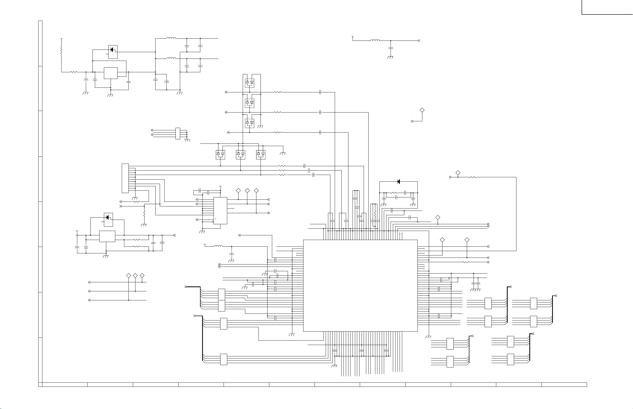
ËË
Ë PC I/F Unit-4/7 (AVC System)
ËË
VA+12
H
R1126
10(1/4W)
R121 0(1/2W)
+
C80
47uF/16V
VREGIN
C81
0.01uF
IC7
PQ05TZ11
1
D20
1SS187
1
2
VINVCVO
GND
5
3
3
2
G
F
CN8
S12B-PH-SM3-TB
E
10
11
12
CLR_SW1
PC_V3
D9
1SS187
1
3
C82
0.01uF
IC8
PQ20VZ11
1
VI
2
VC
2
3
VO
4
VADJ
GND
5
D
C79
47uF/6.3V
VA+5
+
C
ROUT07
OGOUT07
BOUT07
ROUT0
OGOUT0
BOUT0
B
A
VA5REGO
C777
0.1uF
MAIN_VD3
MAIN_HD3
1
2
3
4
5
6
7
8
9
R1089 100
R123 1.6K(1%)
R124 1K(1%)
TL227
PC_C
TL228
TL229
1
1
1
PC_G
PC_B
PC_R
PC_H
PC_V
R137
10K
L1
NLC322522T-3R3M
NLC322522T-3R3M
C83
0.01uF
PC_H
PC_C
VA+3.3AD
C149
0.01uF
L2
+
C84
33uF/10V
+
C564
100uF/6.3V(PXA)
R1076
8 1
2
7
3
6
4
5
EXBV8V103J
VA+3.3AD 3
RI1A[7..0]6
C143
0.01uF
C145
0.01uF
C921 100uF/6.3V(PXA)
MAIN_HD3
MAIN_VD3
HVSEL1
RI1B[7..0]6
VA+5-AMP
+
C144
47uF/10V(PXA-5)
VA+5-PLL
+
C146
33uF/10V
MAIN_R3
MAIN_G3
MAIN_B3
VA+5-AMP
2
D85
K2
MA157A
3
VD+3.3
+
C907
0.1uF
168
2
1A
3
1B
5
2A
6
2B
11
3A
10
3B
14
4A
13
4B
1
A/B
15
G
VD+5
L4
NLC322522T-3R3M
47uF/6.3V
SDA2_51,3
SCL2_53
R959
RI1B0
RI1B1
RI1B2
RI1B3
RI1B4
RI1B5
RI1B6
RI1B7
EXBV8V680J
6
7
7
8
8
6
7
7
8
8
R962
EXBV8V680J
6
7
8
R965
EXBV8V680J
R968
6
7
8
EXBV8V680J
RI1A0
RI1A1
RI1A2
RI1A3
RI1A4
RI1A5
RI1A6
RI1A7
1
D86
A1
MA157A
K1A2
IC411
4
1Y
VCCGND
7
2Y
9
3Y
12
4Y
74LCX157MTC
XPWR_SVO3
C96
VA+5-AMP
VA+3.3AD
45
3
3456
2
2
1
1
45
3
3456
2
2
1
1
45
3
3456
2
2
7
1
1
8
45
3
3456
2
2
7
1
1
8
+
LCRI1B4
LCRI1B5
LCRI1B6
LCRI1B7
D82
MA157A
D83
MA157A
D84
MA157A
2
K2
TL218
1
VD+5-ADC
LC-30HV4E
V-5
L22 NLC322522T-3R3M
1
2
A1
K2
K1A2
3
1
2
A1
K2
K1A2
3
1
2
A1
K2
K1A2
3
2
1
D87
A1
MA157A
K1A2
3
TL219
TL220
1
1
C115
0.1uF
K2
3
1
A1
K1A2
R867
0
R868
0
R869
0
R745 0
R747 0
R749 0
OV0_H 6
OV0_V 6
PC_C3 6
BOUT0
ROUT0
C110
0.1uF
C112
0.1uF
C111
0.1uF
C113
1uF(K)
C114
0.1uF
C116
0.1uF
1
B/CbOUT
2
ADDRESS
3
R/CrOUT
4
NC
5
NC
6
XPOWER SAVE
7
DGNDREG
8
DVCCREG
9
SDA
10
SCL
11
XSENABLE
12
SEROUT
13
3WIRE/IIC
14
DPGND
15
AVCCADREF
16
AVCCAD3
17
VRT
18
DVCCAD3
19
DVCCADTTL
20
DGNDADTTL
21
RA0
22
RA1
23
DGNDAD3
24
RA2
25
RA3
26
RA4
27
RA5
28
RA6
29
AGNDAD3
30
DGNDAD3
31
RA7
32
DVCCADTTL
33
DGNDADTTL
34
RB0
35
RB1
36
RB2
C562
0.1uF
VA+5-AMP
VD+5-ADC
C78
0.1uF
C70
0.1uF
C62
0.1uF
C563
0.1uF
C565
0.1uF
C136 0.1uF
C135 0.1uF
C132
OGOUT0
C138 0.1uF
140
141
142
143
144
R/CrIN2
G/YOUT
AGNDAMPR
DAC TEST OUT
137
138
139
DPGND
R/CrIN1
AVCCAMPR
AGNDAMPB
136
B/CbIN2
C137 0.1uF
134
135
SOGIN2
AVCCAMPB
132
133
B/CbIN1
131
DPGND
SOGIN1
130
R/CrCLP
C134 0.1uF
128
129
G/YCLP
B/CbCLP
C133 0.1uF
125
126
127
G/YIN2
AVCCAMPG
AGNDAMPG
124
123
G/YIN1
IC4
CXA3506R
RB3
RB4
RB5
RB6
RB7
DVCCADTTL
DGNDAD3
DGNDADTTL
BA0
BA1
BA2
BA3
BA4
DGNDAD3
BA5
BA6
BA7
DVCCADTTL
DGNDADTTL
BB0
LCBI1A5
LCBI1A6
0.1uF
C118
LCBI1A7
BB1
LCBI1B1
LCBI1B0
LCBI1B2
3738394041424344454647484950515253545556575859606162636465666768697071
C117 0.1uF
LCBI1A4
LCBI1A1
LCBI1A3
LCBI1A2
LCBI1A0
R133
1uF(K)
121
122
DPGND
AGNDIR
BB2
DGNDAD3
LCBI1B3
3K(1%)
C131
120
IREF
AVCCIR
BB3
BB4
LCBI1B5
LCBI1B4
0.1uF
118
119
RC2
BB5
LCBI1B6
RC1
BB6
D78 1SS380
R132
3.3K(1%)
C566
C130
100pF
114
115
116
117
DGNDPLL
AVCCVCO
AGNDVCO
BB7
DVCCADTTL
DGNDAD3
C119 0.1uF
LCBI1B7
C757
4.7uF/10V(2125)
OV0_HSNR6
330pF(CH)
C126
1uF(K)
110
111
112
113
CLKIN
CLPIN
SYNCIN1
SYNCIN2
DVCCPLL
DSYNC/DIVOUT
DGNDADTTL
GA0
GA1
GA2
GA3
LC0GI1A3
LC0GI1A0
LC0GI1A1
LC0GI1A2
VA-5-AMP
12
C128
0.33uF(PF)
C127
100pF
109
EVEN/ODD
XCLKIN
SOGOUT
XUNLOCK
DGNDPLLTTL
DVCCPLLTTL
AGNDADREF
AVCCAD3
DVCCAD3
DVCCAD
DVCCADTTL
DGNDADTTL
DGNDAD3
AGNDAD3
DGNDAD3
DGNDADTTL
DVCCADTTL
GA4
72
LC0GI1A4
VA+5-PLL
C125
0.1uF
XTLOAD
HOLD
DPGND
1/2CLK
1/2XCLK
CLK
XCLK
VRB
GB7
GB6
GB5
GB4
GB3
GB2
GB1
GB0
GA7
GA6
GA5
VA-5-AMP 3
TL225
1
VD+5-ADC
108
107
106
105
104
103
102
101
100
99
98
97
96
95
94
93
92
91
90
89
88
87
86
85
84
83
82
81
80
79
78
77
76
75
74
73
TL84
LCBI1A7
LCBI1A5
LCBI1A4
LCBI1A3
LCBI1A2
LCBI1A1
LCBI1A0
OV0_PDEN6
1
TL202
C122
1
1uF(K)
C121
0.1uF
C120
0.1uF
R967
6
7
7
8
8
EXBV8V680J
R970
6
7
7
8
8
EXBV8V680J
TL221
1
R128 10
LC0GI1B7
LC0GI1B6
LC0GI1B5
LC0GI1B4
LC0GI1B3
LC0GI1B2
LC0GI1B1
LC0GI1B0
LC0GI1A7
LC0GI1A6
LC0GI1A5
BI1A7
45
BI1A6
3
3456
BI1A5
2
2
BI1A4
1
1
BI1A3
45
BI1A2
3
3456
BI1A1
2
2
BI1A0
1
1
R1109 0
OV0_H
TL83
1
0.1uF
C123
LC0GI1B7
LC0GI1B6
LC0GI1B5
LC0GI1B4
LC0GI1B3
LC0GI1B2
LC0GI1B1
LC0GI1B0
BI1A[7..0] 6
VD+5-ADC
VA+3.3AD
0.1uF
C124
EXBV8V680J
EXBV8V680J
R960
6
7
7
8
8
R963
6
7
7
8
8
VCOXHOLD
OV0_CLP 6,7
OV0_HSNR 6
EVENODD 1
OV0_HSC2 6
OVCLK 6
OGI1B7
45
OGI1B6
3
3456
OGI1B5
2
2
OGI1B4
1
1
OGI1B3
45
OGI1B2
3
3456
OGI1B1
2
2
OGI1B0
1
1
LCBI1B7
LCBI1B6
LCBI1B5LCBI1A6
LCBI1B4
EXBV8V680J
LCBI1B3
LCBI1B2
LCBI1B1
LCBI1B0
EXBV8V680J
R966
6
7
7
8
8
R969
6
7
7
8
8
OGI1B[7..0] 6
LC0GI1A7
LC0GI1A6
LC0GI1A5
LC0GI1A4
LC0GI1A3
LC0GI1A2
LC0GI1A1
LC0GI1A0
BI1B7
45
BI1B6
3
3456
BI1B5
2
2
BI1B4
1
1
BI1B3
45
BI1B2
3
3456
BI1B1
2
2
BI1B0
1
1
R961
6
7
7
8
8
EXBV8V680J
R964
6
7
7
8
8
EXBV8V680J
OGI1A7
45
OGI1A6
3
3456
OGI1A5
2
2
OGI1A4
1
1
OGI1A3
45
OGI1A2
3
3456
OGI1A1
2
2
OGI1A0
1
1
BI1B[7..0] 6
OGI1A[7..0] 6
122
121110987654321
123
Page 94

ËË
Ë PC I/F Unit-5/7 (AVC System)
ËË
A[25..0]1,2
H
G
D[15..0]1,2
F
E
D
C
B
A
-RST_C11
-WAIT_C11
-C1_INT1
CKIO1
-CS21
-RD1,2
-WEL1,2
-WEH1,2
SDD64
SDD65
SDD66
SDD67
SDD68
SDD69
SDD70
SDD71
SDD72
SDD73
SDD74
SDD75
SDD76
SDD77
SDD78
SDD79
SDD80
SDD81
SDD82
SDD83
SDD84
SDD85
SDD86
SDD87
SDD88
SDD89
SDD90
SDD91
SDD92
SDD93
SDD94
SDD95
SDD96
SDD97
SDD98
SDD99
SDD100
SDD101
SDD102
SDD103
SDD104
SDD105
SDD106
SDD107
SDD108 SDD44
SDD109
SDD110
SDD111
SDD112
SDD113
SDD114
SDD115
SDD116
SDD117
SDD118
SDD119
SDD120
SDD121
SDD122
SDD123
SDD124
SDD125
SDD126
SDD127
LC-30HV4E
A0
A1
A2
A3
A4
A5
A6
A7
A8
A9
A10
A11
A12
A13
A14
A15
A16
A17
A18
A19
A20
A21
A22
A23
A24
A25
D1
D2
D3
D4
D5
D6
D7
D8
D9
D10
D11
D12
D13
D14
D15
26
BA_0
25
24
139
23
138
245
22
137
244
21
136
243
342
20
135
242
341
134
241
340
431
133
240
339
430
144
28
143
250
27
142
249
348
141
248
347
247
346
437
345
436
211
140
246
145
252
251
349
350
289
76
77
78
79
190
80
81
295
389
388
292
386
291
385
290
82
83
194
84
85
86
197
198
90
200
301
394
480
393
392
296
472
473
387
475
476
390
556
478
192
294
191
293
189
188
187
384
391
479
481
396
395
302
201
91
199
300
299
196
298
195 284
297
193
IC25A
CVIC2
MCLK
SDMODE0
SDMODE1
XRAS
XCAS
XWE
DQM_0
DQM_1
DQM_2
DQM_3
DQM_4
DQM_5
DQM_6
DQM_7
SDA_0
SDA_1
SDA_2
SDA_3
SDA_4
SDA_5
SDA_6
SDA_7
SDA_8
SDA_9
SDA_10
SDA_11
SDA_12
SDA_13
SDD_0
SDD_1
SDD_2
SDD_3
SDD_4
SDD_5
SDD_6
SDD_7
SDD_8
SDD_9
SDD_10
SDD_11
SDD_12
SDD_13
SDD_14
SDD_15
SDD_16
SDD_17
SDD_18
SDD_19
SDD_20
SDD_21
SDD_22
SDD_23
SDD_24
SDD_25
SDD_26
SDD_27
SDD_28
SDD_29
SDD_30
SDD_31
SDD_32
SDD_33
SDD_34
SDD_35
SDD_36
SDD_37
SDD_38
SDD_39
SDD_40
SDD_41
SDD_42
SDD_43
SDD_44
SDD_45
SDD_46
SDD_47
SDD_48
SDD_49
SDD_50
SDD_51
SDD_52
SDD_53
SDD_54
SDD_55
SDD_56
SDD_57
SDD_58
SDD_59
SDD_60
SDD_62
SDD_63
BA_1
BA_2
BA_3
BA_4
BA_5
BA_6
BA_7
BA_8
BA_9
BA_10
BA_11
BA_12
BA_13
BA_14
BA_15
BA_16
BA_17
BA_18
BA_19
BA_20
BA_21
BA_22
BA_23
BA_24
BA_25
BD_0
BD_1
BD_2
BD_3
BD_4
BD_5
BD_6
BD_7
BD_8
BD_9
BD_10
BD_11
BD_12
BD_13
BD_14
BD_15
XRESET
BWAIT
BINT
BCLK
XBCS
RD
XBWE_0
XBWE_1
SDD_64
SDD_65
SDD_66
SDD_67
SDD_68
SDD_69
SDD_70
SDD_71
SDD_72
SDD_73
SDD_74
SDD_75
SDD_76
SDD_77
SDD_78
SDD_79
SDD_80
SDD_81
SDD_82
SDD_83
SDD_84
SDD_85
SDD_86
SDD_87
SDD_88
SDD_89
SDD_90
SDD_91
SDD_92
SDD_93
SDD_94
SDD_95
SDD_96
SDD_97
SDD_98
SDD_99
SDD_100
SDD_101
SDD_102
SDD_103
SDD_104
SDD_105
SDD_106
SDD_107
SDD_108
SDD_109
SDD_110
SDD_111
SDD_112
SDD_113
SDD_114
SDD_115
SDD_116
SDD_117
SDD_118
SDD_119
SDD_120
SDD_121
SDD_122
SDD_123
SDD_124
SDD_125 SDD_61
SDD_126
SDD_127
NC3
NC2
NC1
XCS
XRAS
DQM[7..0]
SDA[10..0]
MCLK
SDD[127..0]
25
IC319
DQ10
DQ11
DQ12
DQ13
DQ14
DQ15
DQ16
DQ17
DQ18
DQ19
DQ20
DQ21
DQ22
DQ23
DQ24
DQ25
DQ26
DQ27
DQ28
DQ29
DQ30
DQ31
DQM0
DQM1
DQM2
DQM3
DQ0
DQ1
DQ2
DQ3
DQ4
DQ5
DQ6
DQ7
DQ8
DQ9
NC
NC
NC
NC
NC
NC
NC
C5760.1uF
C5820.1uF
A0
26
A1
27
A2
60
A3
61
A4
62
A5
63
A6
64
A7
65
A8
66
A9
24
A10(AP)
22
BA0
23
BA1
68
CLK
67
CKE
20
/CS
19
/RAS
18
/CAS
17
/WE
3
VccQ
9
VccQ
35
VccQ
41
VccQ
49
VccQ
55
VccQ
75
VccQ
81
VccQ
6
VssQ
12
VssQ
32
VssQ
38
VssQ
46
VssQ
52
VssQ
78
VssQ
84
VssQ
1
Vcc
15
Vcc
29
Vcc
43
Vcc
44
Vss
58
Vss
72
Vss
86
Vss
SDA1
SDA2
SDA3
SDA4
SDA5
SDA6
SDA7
SDA8
SDA9
SDA10
SD_BA0
SD_BA1
R696 10K
VD+3.3 VD+3.3
FL94
3
BMK351
V_DRAM1
1
I
O
G
+
2
100uF/4V
C573
C5800.1uF
C5790.1uF
C5810.1uF C5750.1uFC5950.1uF
SDD0SDA0D0
2
SDD1
4
SDD2
5
SDD3
7
SDD4
8
SDD5
10
SDD6
11
SDD7
13
SDD8
74
SDD9
76
SDD10
77
SDD11
79
SDD12
80
SDD13
82
SDD14
83
SDD15
85
SDD16
31
SDD17
33
SDD18
34
SDD19
36
SDD20
37
SDD21
39
SDD22
40
SDD23
42
SDD24
45
SDD25
47
SDD26
48
SDD27
50
SDD28
51
SDD29
53
SDD30
54
SDD31
56
DQM0
16
71
28
DQM1
59
14
21
30
57
69
70
73
SDA0
SDA1
SDA2
SDA3
SDA4
SDA5
SDA6
SDA7
SDA8
SDA9
SDA10
SD_BA0
SD_BA1
HY57V653220BTC-7
SDA0
SDA1
SDA2
SDA3
SDA4
SDA5
SDA6
SDA7
SDA8
SDA9
SDA10
SD_BA0
SD_BA1
R698 10K
C5940.1uF
C5930.1uF
V_DRAM1
C5890.1uF
C5900.1uF
C5960.1uF
25
IC321
DQ10
DQ11
DQ12
DQ13
DQ14
DQ15
DQ16
DQ17
DQ18
DQ19
DQ20
DQ21
DQ22
DQ23
DQ24
DQ25
DQ26
DQ27
DQ28
DQ29
DQ30
DQ31
DQM0
DQM1
DQM2
DQM3
DQ0
DQ1
DQ2
DQ3
DQ4
DQ5
DQ6
DQ7
DQ8
DQ9
NC
NC
NC
NC
NC
NC
NC
A0
26
A1
27
A2
60
A3
61
A4
62
A5
63
A6
64
A7
65
A8
66
A9
24
A10(AP)
22
BA0
23
BA1
68
CLK
67
CKE
20
/CS
19
/RAS
18
/CAS
17
/WE
3
VccQ
9
VccQ
35
VccQ
41
VccQ
49
VccQ
55
VccQ
75
VccQ
81
VccQ
6
VssQ
12
VssQ
32
VssQ
38
VssQ
46
VssQ
52
VssQ
78
VssQ
84
VssQ
1
Vcc
15
Vcc
29
Vcc
43
Vcc
44
Vss
58
Vss
72
Vss
86
Vss
SDD32
2
SDD33
4
SDD34
5
SDD35
7
SDD36
8
SDD37
10
SDD38
11
SDD39
13
SDD40
74
SDD41
76
SDD42
77
SDD43
79
SDD44
80
SDD45
82
SDD46
83
SDD47
85
SDD48
31
SDD49
33
SDD50
34
SDD51
36
SDD52
37
SDD53
39
SDD54
40
SDD55
42
SDD56
45
SDD57
47
SDD58
48
SDD59
50
SDD60
51
SDD61
53
SDD62
54
SDD63
56
DQM2
16
71
DQM3
28
59
14
21
30
57
69
70
73
SDA0
SDA1
SDA2
SDA3
SDA4
SDA5
SDA6
SDA7
SDA8
SDA9
SDA10
SD_BA0
SD_BA1
HY57V653220BTC-7
R689 470
FL95
BMK351
3
O
I
G
2
C5830.1uF
C5970.1uF
VD+3.3CV
R697 10K
1
+
100uF/4V
C574
C5770.1uF
C5850.1uF
C5840.1uF
R699 10K
C5910.1uF
C5990.1uF
C5980.1uF
V_DRAM1
C5780.1uF
C5860.1uF
C5920.1uF
C6000.1uF
25
26
27
60
61
62
63
64
65
66
24
22
23
68
67
20
19
18
17
3
9
35
41
49
55
75
81
6
12
32
38
46
52
78
84
1
15
29
43
44
58
72
86
25
26
27
60
61
62
63
64
65
66
24
22
23
68
67
20
19
18
17
3
9
35
41
49
55
75
81
6
12
32
38
46
52
78
84
1
15
29
43
44
58
72
86
A0
IC320
A1
A2
A3
A4
A5
A6
A7
A8
A9
A10(AP)
BA0
BA1
CLK
CKE
/CS
/RAS
/CAS
/WE
VccQ
VccQ
VccQ
VccQ
VccQ
VccQ
VccQ
VccQ
VssQ
VssQ
VssQ
VssQ
VssQ
VssQ
VssQ
VssQ
Vcc
Vcc
Vcc
Vcc
Vss
Vss
Vss
Vss
HY57V653220BTC-7
A0
IC322
A1
A2
A3
A4
A5
A6
A7
A8
A9
A10(AP)
BA0
BA1
CLK
CKE
/CS
/RAS
/CAS
/WE
VccQ
VccQ
VccQ
VccQ
VccQ
VccQ
VccQ
VccQ
VssQ
VssQ
VssQ
VssQ
VssQ
VssQ
VssQ
VssQ
Vcc
Vcc
Vcc
Vcc
Vss
Vss
Vss
Vss
DQ0
DQ1
DQ2
DQ3
DQ4
DQ5
DQ6
DQ7
DQ8
DQ9
DQ10
DQ11
DQ12
DQ13
DQ14
DQ15
DQ16
DQ17
DQ18
DQ19
DQ20
DQ21
DQ22
DQ23
DQ24
DQ25
DQ26
DQ27
DQ28
DQ29
DQ30
DQ31
DQM0
DQM1
DQM2
DQM3
DQ0
DQ1
DQ2
DQ3
DQ4
DQ5
DQ6
DQ7
DQ8
DQ9
DQ10
DQ11
DQ12
DQ13
DQ14
DQ15
DQ16
DQ17
DQ18
DQ19
DQ20
DQ21
DQ22
DQ23
DQ24
DQ25
DQ26
DQ27
DQ28
DQ29
DQ30
DQ31
DQM0
DQM1
DQM2
DQM3
HY57V653220BTC-7
SDD64
2
SDD65
4
SDD66
5
SDD67
7
SDD68
8
SDD69
10
SDD70
11
SDD71
13
SDD72
74
SDD73
76
SDD74
77
SDD75
79
SDD76
80
SDD77
82
SDD78
83
SDD79
85
SDD80
31
SDD81
33
SDD82
34
SDD83
36
SDD84
37
SDD85
39
SDD86
40
SDD87
42
SDD88
45
SDD89
47
SDD90
48
SDD91
50
SDD92
51
SDD93
53
SDD94
54
SDD95
56
DQM4
16
DQM5
71
28
59
14
NC
21
NC
30
NC
57
NC
69
NC
70
NC
73
NC
SDD96
2
SDD97
4
SDD98
5
SDD99
7
SDD100SDD24
8
SDD101
10
SDD102
11
SDD103
13
SDD104
74
SDD105
76
SDD106
77
SDD107
79
SDD108
80
SDD109
82
SDD110
83
SDD111
85
SDD112
31
SDD113
33
SDD114
34
SDD115
36
SDD116
37
SDD117
39
SDD118
40
SDD119
42
SDD120
45
SDD121
47
SDD122
48
SDD123
50
SDD124
51
SDD125
53
SDD126
54
SDD127
56
DQM6
16
71
28
DQM7
59
14
NC
21
NC
30
NC
57
NC
69
NC
70
NC
73
NC
179
440
416
537
92
202
57
170
371
274
272
369
55
168
273
370
56
169
51
164
269
367
270
165
52
271
166
53
368
457
54
167
61
63
64
65
66
67
178
68
376
463
375
279
278
277
173
275
69
70
181
71
72
73
74
75
383
288
287
286
285
379
378
377
276
459
372
373
460
374
461
541
281
280
177
176
175
174
62
172
464
466
380
467
381
382
469
470
186
185
184
183
182
180
282
R692 0
R694 0
R693 0
R695 0
R688 0
XCS
XCAS
XWE
DQM0
DQM1
DQM2
DQM3
DQM4
DQM5
DQM6
DQM7
SDA0
SDA1
SDA2
SDA3
SDA4
SDA5
SDA6
SDA7
SDA8
SDA9
SDA10
SD_BA0
SD_BA1
SDD0
SDD1
SDD2
SDD3
SDD4
SDD5
SDD6
SDD7
SDD8
SDD9
SDD10
SDD11
SDD12
SDD13
SDD14
SDD15
SDD16
SDD17
SDD18
SDD19
SDD20
SDD21
SDD22
SDD23
SDD25
SDD26
SDD27
SDD28
SDD29
SDD30
SDD31
SDD32
SDD33
SDD34
SDD35
SDD36
SDD37
SDD38
SDD39 V_DRAM1
SDD40
SDD41
SDD42
SDD43
SDD45
SDD46
SDD47
SDD48
SDD49
SDD50
SDD51
SDD52
SDD53
SDD54
SDD55
SDD56
SDD57
SDD58
SDD59
SDD60
SDD61
SDD62
SDD63
124
121110987654321
125
Page 95

ËË
Ë PC I/F Unit-6/7 (AVC System)
ËË
RI1A[7..0]4
H
OGI1A[7..0]4
BI1A[7..0]4
G
RI1B[7..0]4
OGI1B[7..0]4
F
BI1B[7..0]4
OVCLK4
OV0_H4
OV0_V4
E
PC_C34
OV0_HSC24
OVR[7..0]3
OVG[7..0]3
D
OVB[7..0]3
C
OV1_VCLK3
OV1_H3
OV1_V3
B
RI1A0
RI1A1
RI1A2
RI1A3
RI1A4
RI1A5
RI1A6
RI1A7
OGI1A0
OGI1A1
OGI1A2
OGI1A3
OGI1A4
OGI1A5
OGI1A6
OGI1A7
BI1A0
BI1A1
BI1A2
BI1A3
BI1A4
BI1A5
BI1A6
BI1A7
RI1B0
RI1B1
RI1B2
RI1B3
RI1B4
RI1B5
RI1B6
RI1B7
OGI1B0
OGI1B1
OGI1B2
OGI1B3
OGI1B4
OGI1B5
OGI1B6
OGI1B7
BI1B0
BI1B1
BI1B2
BI1B3
BI1B4
BI1B5
BI1B6
BI1B7
R977 10K
OVR0
OVR1
OVR2
OVR3
OVR4
OVR5
OVR6
OVR7
OVG0
OVG1
OVG2
OVG3
OVG4
OVG5
OVG6
OVG7
OVB0
OVB1
OVB2
OVB3
OVB4
OVB5
OVB6
OVB7
104
213
214
315
408
493
317
318
485
400
307
206
96
399
306
205
404
311
488
403
310
209
100
99
103
314
407
405
312
102
210
101
398
305
204
95
304
203
94
93
402
309
208
401
308
207
98
97
320
412
494
216
105
106
215
316
107
409
113
221
108
217
411
496
109
319
219
220
10
11
126
233
332
234
333
424
121
229
123
230
329
421
321
413
118
112
228
327
328
419
120
111
115
223
117
119
226
325
326
417
12
127
13
128
235
334
425
14
124
231
330
125
232
331
422
V0_RA0
V0_RA1
V0_RA2
V0_RA3
V0_RA4
V0_RA5
V0_RA6
V0_RA7
V0_GA0
V0_GA1
V0_GA2
V0_GA3
V0_GA4
V0_GA5
V0_GA6
V0_GA7
V0_BA0
V0_BA1
V0_BA2
V0_BA3
V0_BA4
V0_BA5
V0_BA6
V0_BA7
V0_RB0
V0_RB1
V0_RB2
V0_RB3
V0_RB4
V0_RB5
V0_RB6
V0_RB7
V0_GB0
V0_GB1
V0_GB2
V0_GB3
V0_GB4
V0_GB5
V0_GB6
V0_GB7
V0_BB0
V0_BB1
V0_BB2
V0_BB3
V0_BB4
V0_BB5
V0_BB6
V0_BB7
V0_PVDCLK
V0_NVDCLK
V0_VDCLK_I
V0_VAL
V0_HSYNC
V0_VSYNC
V0_CSYNC
V0_GSYNC
V0_HSYNC2
V0_ACT
V0_PVCLK
V0_NVCLK
V1_RA0
V1_RA1
V1_RA2
V1_RA3
V1_RA4
V1_RA5
V1_RA6
V1_RA7
V1_GA0
V1_GA1
V1_GA2
V1_GA3
V1_GA4
V1_GA5
V1_GA6
V1_GA7
5
V1_BA0
V1_BA1
V1_BA2
V1_BA4
V1_BA5
V1_BA6
V1_BA7
V1_PVDCLK
V1_NVDCLK
V1_VDCLK_I
V1_VAL
V1_HSYNC
V1_VSYNC
V1_CSYNC
V1_GSYNC
V1_HSYNC2
V1_ACT
V1_PVCLK
V1_NVCLK
V1_RB0
3
V1_RB1
4
V1_RB2
V1_RB3
V1_RB4
V1_RB5
V1_RB6
V1_RB7
V1_GB0
V1_GB1
V1_GB2
V1_GB3
V1_GB4
V1_GB5
V1_GB6
V1_GB7
9
V1_BB0
V1_BB1
V1_BB2
V1_BB3
V1_BB4
V1_BB5
V1_BB6
V1_BB7
CVIC2
A
IC25B
DO_RA0
DO_RA1
DO_RA2
DO_RA3
DO_RA4
DO_RA5
DO_RA6
DO_RA7
DO_RA8
DO_RA9
DO_GA0
DO_GA1
DO_GA2
DO_GA3
DO_GA4
DO_GA5
DO_GA6
DO_GA7
DO_GA8
DO_GA9
DO_BA0
DO_BA1
DO_BA2
DO_BA3
DO_BA4
DO_BA5
DO_BA6
DO_BA7
DO_BA8
DO_BA9
DO_RB0
DO_RB1
DO_RB2
DO_RB3
DO_RB4
DO_RB5
DO_RB6
DO_RB7
DO_RB8
DO_RB9
DO_GB0
DO_GB1
DO_GB2
DO_GB3
DO_GB4
DO_GB5
DO_GB6
DO_GB7
DO_GB8
DO_GB9
DO_BB0
DO_BB1
DO_BB2
DO_BB3
DO_BB4
DO_BB5
DO_BB6
DO_BB7
DO_BB8
DO_BB9
DO_HSYNC
DO_VSYNC
DO_HDISP
DO_VDISP
DO_FEILD
V0_VDCLK_O
V0_PADCLK
V0_NADCLK
V0_PADRST
V0_NADRST
V0_CLP
V0_HSYNR
V0_HSYNF
V0_PDEN
V1_VDCLK_O
V1_PADCLK
V1_NADCLK
V1_PADRST
V1_NADRST
V1_CLP
V1_HSYNRV1_BA3
V1_HSYNF
V1_PDEN
BIASIN_VI
BIASOUT_VI
BIASIN_DO
BIASOUT_DO
DCLK
LCLK
LCLKP
LCLKN
S0_D0
S0_D1
S0_D2
S0_D3
S1_D0
S1_D1
S1_D2
S1_D3
MCK_REF
PLL_S
PLL_TEST
MST
XTST
SMCK
XSM
IMODE
INITO
INITI
CPUS_0
CPUS_1
CPUS_2
CPUS_3
CCS_0
CCS_1
LC-30HV4E
FL98
33(1/10W)
123
FL110
0(1/10W)
R1201 100
RSI[9..2] 7
OGSI[9..2] 7
BSI[9..2] 7
DCLKXTAL
123
R1135
10K
TL114
1
R1128
47
X4
3 4
OUTVDC
DSO751SV(25.000M)
LCLK 7
12
CntlGND
X6
3 4
OUTVDC
CntlGND
DSO751SV(25.175M)
X5
3 4
OUTVDC
CntlGND
91.3M
VD+3.3
C697
0.01uF
IC25C
1
VSS
2
VSS
29
VSS
30
VSS
31
VSS
32
VSS
58
VSS
59
VSS
60
VSS
87
VSS
88
VSS
89
VSS
116
VSS
283
VSS
338
VSS
344
VSS
352
VSS
353
VSS
433
VSS
443
VSS
455
VSS
482
VSS
484
VSS
501
VSS
502
VSS
503
VSS
506
VSS
507
VSS
510
VSS
511
VSS
514
VSS
515
VSS
519
VSS
520
VSS
521
VSS
522
VSS
525
VSS
526
VSS
529
VSS
530
VSS
533
VSS
534
VSS
538
VSS
539
VSS
540
VSS
544
VSS
545
VSS
548
VSS
549
VSS
552
VSS
553
VSS
557
VSS
558
VSS
559
VSS
563
VSS
564
VSS
567
VSS
568
VSS
571
VSS
572
VSS
576
VSS
3
FL30
BMK351
O
CVIC2
491
A_VDD
490
A_VSS
FL29 BMK351
3
I
O
G
2
FL31 BMK351
3
O
2
1
I
G
2
O
1
1
I
G
PCVICPLL
C846
1uF
R1134
47
VD+3.3 VD+3.3CV
VGA_OE 1
VD+3.3
12
12
C919
0.01uF
VD+3.3
C759
0.01uF
WXGA_OE 1
VD+1.8
3
FL32
BMK351
VDDL
VDDL
VDDL
VDDL
VDDL
VDDL
VDDL
VDDL
VDDL
VDDL
VDDL
VDDL
VDDL
VDDL
VDDL
VDDL
VDDL
VDDL
VDDL
VDDL
VDDL
VDDL
VDDL
VDDL
VDDL
VDDL
VDDL
VDDL
VDDL
VDDL
VDDL
VDDL
VDDH
VDDH
VDDH
VDDH
VDDH
VDDH
VDDH
VDDH
VDDH
VDDH
VDDH
VDDH
VDDH
VDDH
VDDH
VDDH
VDDH
VDDH
VDDH
VDDH
VDDH
VDDH
VDDH
VDDH
VDDH
VDDH
VDDH
VDDH
VDDH
VDDH
VDDH
VDDH
VDDH
VDDH
VDDH
1
I
G
2
+
C367
100uF/6.3V(PXA)
504
505
508
509
512
513
516
517
523
524
527
528
531
532
535
536
542
543
546
547
550
551
554
555
561
562
565
566
569
570
573
574
171
337
343
420
423
426
428
429
432
434
435
438
439
441
442
444
447
450
453
454
456
458
462
465
468
471
474
477
483
486
489
492
495
498
560
+
C366
100uF/6.3V(PXA)
VD+2.5CV
C10
10uF(3225)
C815 0.1uF
C816 0.1uF
C817 0.1uF
C818 0.1uF
C819 0.1uF
C820 0.1uF
C821 0.1uF
C822 0.1uF
C823 0.1uF
C824 0.1uF
C825 0.1uF
C826 0.1uF
C827 0.1uF
C828 0.1uF
C829 0.1uF
C830 0.1uF
C831 0.1uF
C832 0.1uF
C833 0.1uF
C834 0.1uF
C835 0.1uF
C836 0.1uF
C837 0.1uF
C838 0.1uF
C839 0.1uF
C840 0.1uF
C841 0.1uF
C842 0.1uF
C843 0.1uF
C844 0.1uF
C845 0.1uF
C848 0.1uF
C15
10uF(3225)
C850
100uF/6.3V(PXA)
100uF/6.3V(PXA)
TP10
PAD1.6
VD+1.8
+
TP11
PAD1.6
C847
100uF/6.3V
C851
VD+5
C849
100uF/6.3V
VD+3.3
+
TP12
PAD1.6
+
C852
47uF/6.3V
VA+5
TP13
PAD1.6
FL205 NFM21PC105B1A3D
3
O
I
G
2
FL206 NFM21PC105B1A3D
3
I
O
+
V-5
+
G
2
FL207 NFM21PC105B1A3D
3
I
O
2
FL208 NFM21PC105B1A3D
3
I
O
2
VA+12
+
VD+5BK
C854
47uF/16V
VD+5IN
1
VA+5IN
1
VD+1.8IN
1
G
VD+3.3IN
1
G
C853
0.01uF
CN9
S13B-PH-SM3-TB
1
1
2
2
3
3
4
4
5
5
6
6
7
7
8
8
9
9
10
10
11
11
12
12
13
13
R971 EXBV8V330J
RSI2
355
354
257
152
39
256
151
38
150
37
446
357
445
356
259
154
41
258
153
40
448
359
262
358
261
156
43
260
155
42
361
264
159
449
360
263
158
45
157
44
452
363
266
161
451
362
265
160
47
46
366
365
268
163
50
364
267
162
49
48
R978 0
36
R979 0
35
R980 0
149
254
148
225
114
222
322
414
218
406
313
410
227
224
324
415
499
110
68
7
122
323
575
253
351
146
255
33
147
236
129
15
16
427
336
130
131
497
IPD
212
487
397
303
418
500
518
34
17
335
132
239
238
237
19
18
TL122
1
DCLKIN
-RST_PLL 1
VD+3.3CV
TL222
1
OV0_CLP 4,7
OV0_HSNR 4
OV0_PDEN 4
OV1_VCKO 3
OV1_CLP 3
OV1_HSNR 3
OV1_HSNF 3
OV1_PDEN 3
45
3
6
3456
2
7
2
7
1
8
1
8
R972 EXBV8V330J
45
3
6
3456
2
7
2
7
1
8
1
8
R973 EXBV8V330J
1
8
8
1
2
7
7
2
3
6
3456
45
R974 EXBV8V330J
45
3
6
3456
2
7
2
7
1
8
1
8
R975 EXBV8V330J
1
8
1
8
2
7
2
7
3
6
3456
45
R976 EXBV8V330J
1
8
1
8
2
7
2
7
3
6
3456
45
TL112
TL113
1
1
RSI3
RSI4
RSI5
RSI6
RSI7
RSI8
RSI9
OGSI2
OGSI3
OGSI4
OGSI5
OGSI6
OGSI7
OGSI8
OGSI9
BSI2
BSI3
BSI4
BSI5
BSI6
BSI7
BSI8
BSI9
DO_HSYNC 7
DO_VSYNC 1,7
DO_HDISP 1,7
126
121110987654321
127
Page 96

ËË
Ë PC I/F Unit-7/7 (AVC System)
ËË
H
G
C858
82pF
VD+3.3
C859
0.1uF
+
C860
10uF/16V
L100
0(3216)
FL200
3
BLM31PG121SN1
O
2
G
I
1
0(3216)
L101
FL201
3
I
O
G
BLM31PG121SN1
2
LC-30HV4E
1
C855
82pF
C856
0.1uF
C857
+
10uF/16V
R1101
CSEN13
CSEN23
SRST3
FLASH_W3
TXD0_M1
RXD0_M1
SMPOW3
SENCE3
FWMODEN2
5
6
7
8 1
EXBV8V560J
R1102
5
6
7
8 1
EXBV8V560J
CSEN1CN
4
CSEN2CN
3
2
SRSTCN
FLASHWCN
CCKM
TXD0CN
4
RXD0CN
3
SMPOWCN
2
SENCECN
VD+5BK
CN1
1
2
3
4
5
6
7
8
9
10
11
12
13
14
15
SM15B-SRSS-TB
CCKM
R1009
2.2K
R1006
2.2K
2
VD+5
1 3
Q103
2SC2412KQ
R1012
1K
R1011 33K
CCK 1
RSI[9..2]6
OGSI[9..2]6
BSI[9..2]6
VD+5
6
5
TL223
PAD1.6
D75
1SS187
1
3
2
V_SII
+
VD+3.3
TL224
PAD1.6
1
1
10uF/16V
0.1uF
TP4
TESTPIN
TL231
PAD1.6
1
C869
C867
OGSI5
OGSI4
OGSI3
OGSI2
BSI9
BSI8
BSI7
BSI6
BSI5
BSI4
BSI3
BSI2
DO_HDISP1,6
DO_HSYNC6
DO_VSYNC1,6
MON_DET1
-RST_PL1
SCL11
SDA_11
LCLK6
82pF
C872
0.1uF
C874
C864
82pF
49
PVCC2
50
D11
51
D10
52
D9
53
D8
54
D7
55
D6
56
IDCK-
57
IDCK+
58
D5
59
D4
60
D3
61
D2
62
D1
63
D0
64
GND
F
VD+3.3
IC412
1
VC
VIN
2
GND
GND1
3 4
NR VO
PQ1R33
C868
0.1uF
E
D
48
R1007
1K
OGSI6
OGSI7
PGND2
D12/DUAL
DE
VCC
23456
OGSI8
D13/MASI
VREF
RSI2
RSI3
RSI4
RSI5
RSI6
OGSI9
V_SII_VD
D19
D18
D17
D16
D15
D14/SYNCO
IC413
SiI170
DK1/MCL
HSYNC/SYNC1
VSYNC
DK3
DK2/MDA
EDGE/CHGPDVCC
8
719101213141516
R1008
RSI7
RSI8
RSI9
C863
82pF
333435363738394041424344454647
D23
D22
D21
D20
VCC
GND
32
AGND
RESERVED
31
TX2+
30
TX2-
29
AVCC
28
TX1+
27
TX1-
26
AGND
25
TX0+
24
TX0-
23
AVCC
22
TXC+
21
TXC-
20
AGND
19
EXT_SWING
18
PVCCI
17
PGND1
ISEL/RST
DSEL/SDA
BSEL/SCL
GND
MSEN
11
R1002 100
R1003 100
1K
C879
82pF
V_SII_VA
C865
82pF
C870
82pF
R999 510
C875
82pF
C876
0.1uF
DV_TXD2+
DV_TXD2-
DV_TXD1+
DV_TXD1-
DV_TXD0+
DV_TXD0-
DV_TXDC+
DV_TXDC-
VD+3.3
Q102
1
G1
2
S2
3 4
G2 D2
NDC7002N
D1
S1
DV_TXD2-
DV_TXD1-
DV_TXD0-
DV_TXDC+
6
5
H1H2
CN3
1 2
D2- D2+
3 4
D2/4SH D4-
5 6
7 8
9 10
11 12
13 14
15 16
17 18
19 20
21 22
23 24
C1 C2
C3 C4
C5
HOOK1HOOK2
D4+ DDC_CLK
DDC_DATA AVSYN
D1- D1+
D1/3SH D3D3+ +5V
GND HOTPD
D0- D0+
D0/5SH D5D5+ CLKSH
CLK+ CLKRED GREEN
BLUE AHSYNC
AGND
AGND
74320-1007
VD+5BK
R1000
1.8K
1.8K
C6
R1001
DV_TXD2+
DV_TXD1+
R1104 100
DV_TXD0+
DV_TXDC-
VD+5DVI
HOTPLUG 1
FL204
3
O
BMK351
SCL1_5 3
SDA1_5 3
VD+5
1
I
G
2
C
ROUT0 4
OGOUT0 4
B
BOUT0 4
R1043
R1042
1K
R1044
1K
1K
A
121110987654321
128
129
Page 97

ËË
Ë LCD CONTROL Unit-1/5 (Display)
ËË
H
G
F
LC-30HV4E
E
D
C
B
A
121110987654321
130
131
Page 98

ËË
Ë LCD CONTROL Unit-2/5 (Display)
ËË
H
G
F
LC-30HV4E
E
D
C
B
A
121110987654321
132
133
Page 99
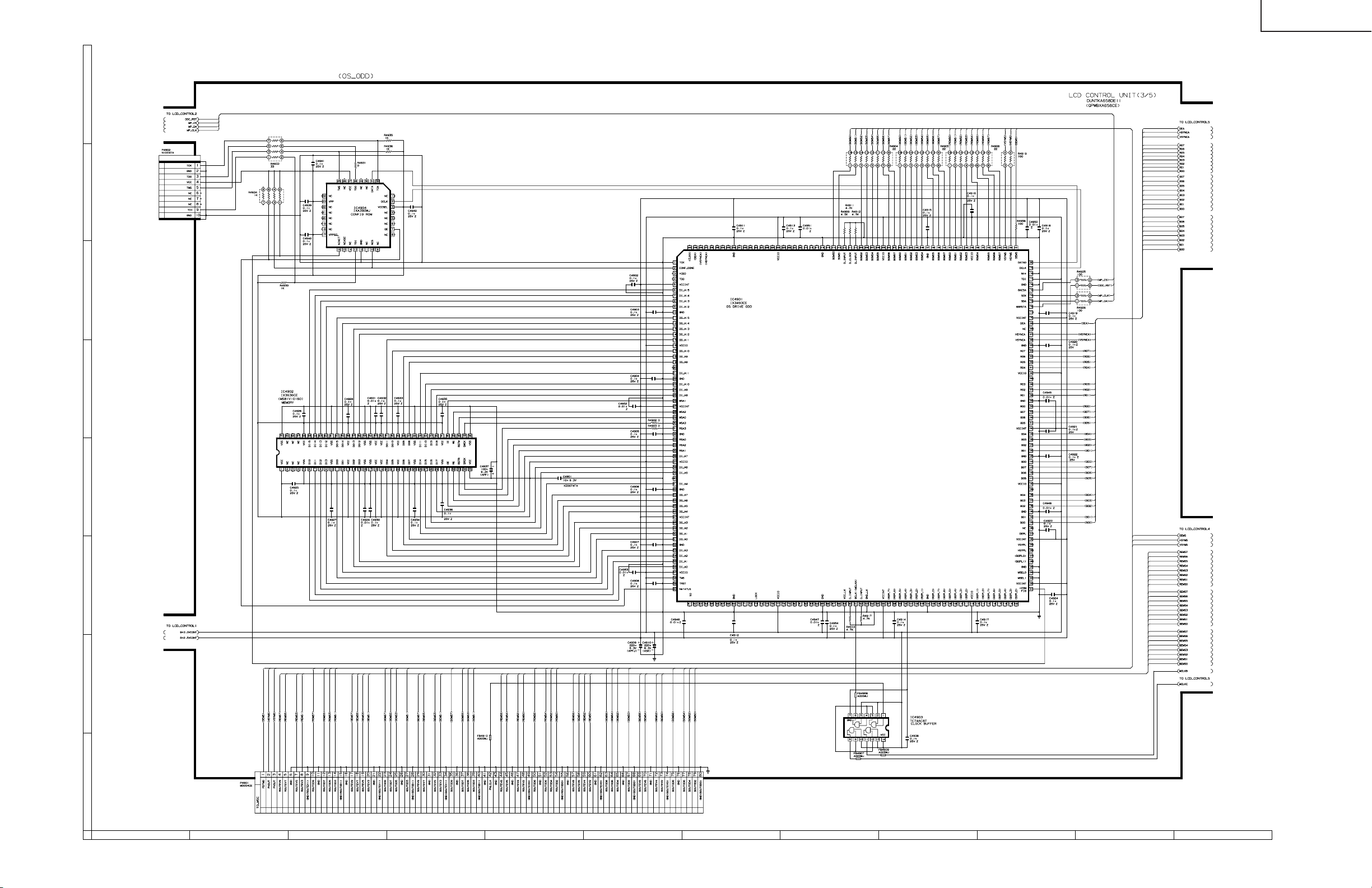
ËË
Ë LCD CONTROL Unit-3/5 (Display)
ËË
H
G
F
LC-30HV4E
E
D
C
B
A
121110987654321
134
135
Page 100

ËË
Ë LCD CONTROL Unit-4/5 (Display)
ËË
H
G
F
LC-30HV4E
E
D
C
B
A
121110987654321
136
137
 Loading...