

Page 1
LC-30HV2E
SERVICE MANUAL
オートセーブ
オンタイマー
電源
MODEL
In the interests of user-safety (Required by safety regulations in some countries) the set should be restored
to its original condition and only parts identical to those specified should be used.
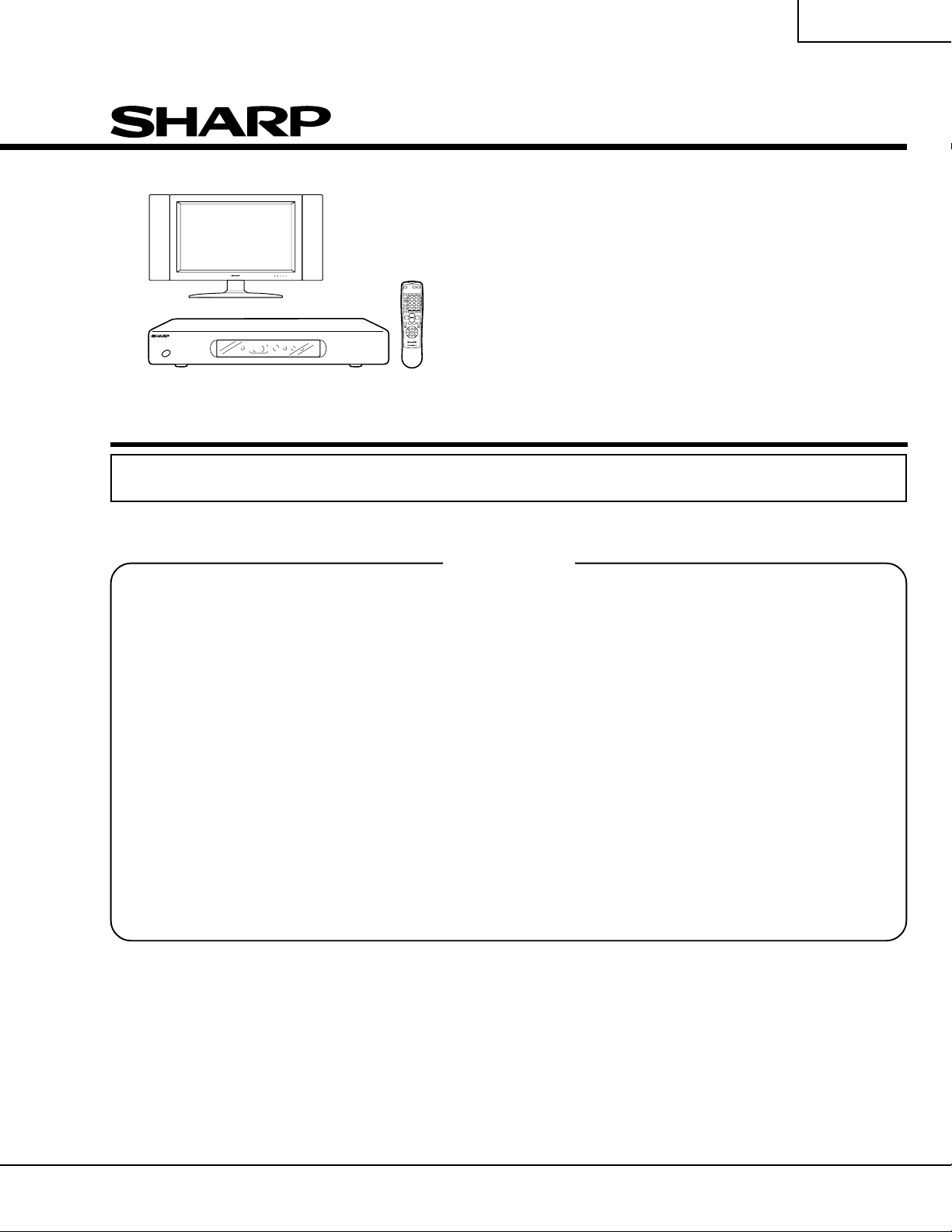
LCD TV
LC-30HV2E
CONTENTS
Page
» IMPORT ANT SERVICE SAFETY PRECAUTION .....2
» SPECIFICATIONS................................................3
» OPERA TION MANUAL ........................................4
» DIMENSIONS ....................................................10
» REMOVING OF MAJOR PARTS........................12
» ADJUSTMENT PROCEDURES.........................19
» DESCRIPTION OF MAJOR IC FUNCTIONS ....30
» TROUBLE SHOOTING TABLE ..........................56
»PRINTED WIRING BOARD BLOCK DIAGRAM..63
» LCD DISPLAY CHASSIS LAYOUT ....................65
» AVC SYSTEM BLOCK DIAGRAM ..................... 68
» AVC SIGNAL FLOW BLOCK DIAGRAM ...........70
» AVC DC/DC CONVERTER BLOCK DIAGRAM .72
» AVC POWER BLOCK DIAGRAM ......................74
» PC I/F BLOCK DIAGRAM..................................76
» LCD DISPLAY SIGNAL BLOCK DIAGRAM...... 76
» LCD DISPLAY POWER UNIT BLOCK
DIAGRAM ..........................................................76
» AVC OVERALL WIRING DIAGRAM .................. 82
» LCD DISPLAY OVERALL WIRING DIAGRAM ..86
» DESCRIPTION OF SCHEMATIC DIAGRAM.....88
» WAVEFORMS ....................................................89
» SCHEMATIC DIAGRAM ....................................90
» PRINTED WIRING BOARD ASSEMBLIES .....160
» PARTS LIST.....................................................175
» PACKING OF THE SET ...................................215
Page
SHARP CORPORATION
Page 2
LC-30HV2E
2
2
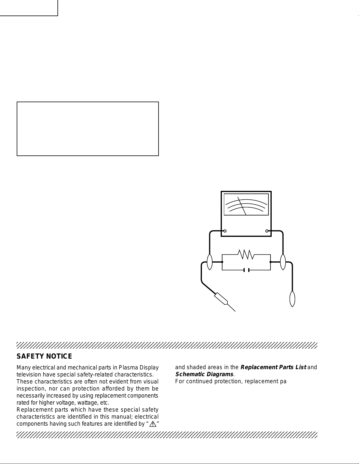
IMPORTANT SERVICE SAFETY PRECAUTION
Ë
Service work should be perfomed only by qualified service technicians who are thoroughly familiar with all safety checks and the servicing guidelines which follow:
WARNING
» Use an AC voltmeter having with 5000 ohm per volt,
or higher, sensitivity or measure the AC voltage drop
1. For continued safety, no modification of any circuit
should be attempted.
2. Disconnect AC power before servicing.
across the resisor.
» Connect the resistor connection to all exposed metal
parts having a return to the chassis (antenna, metal
cabinet, screw heads, knobs and control shafts,
CAUTION: FOR CONTINUED PROTECTION
AGAINST A RISK OF FIRE REPLACE ONLY WITH
SAME TYPE FUSE.
AVC SIDE: F701 (T2A, 250V), F702 (T2A, 250V),
F1702 (T4AL, 250V) FUSE.
LCD SIDE: F1(T3.5AL, 250V), F6551, F6552, F6553,
F6554, F6555, F6556 (T2.5AL, 250V)
escutcheon, etc.) and measure the AC voltage drop
across the resistor.
All checks must be repeated with the AC cord plug
connection reversed. (If necessary, a nonpolarized
adaptor plug must be used only for the purpose of
completing these checks.)
Any reading of 35V peak (this corresponds to 0.7
milliamp. peak AC.) or more is excessive and
BEFORE RETURNING THE RECEIVER
(Fire & Shock Hazard)
indicates a potential shock hazard which must be
corrected before returning the monitor to the owner .
Before returning the receiver to the user, perform
the following safety checks:
1. Inspect all lead dress to make certain that leads are
not pinched, and check that hardware is not lodged
between the chassis and other metal parts in the
receiver.
2. Inspect all protective devices such as non-metallic
control knobs, insulation materials, cabinet backs,
adjustment and compartment covers or shields,
isolation resistor-capacitor networks, mechanical
DVM
AC SCALE
50k ohm
10W
insulators, etc.
3. To be sure that no shock hazard exists, check for
leakage current in the following manner.
» Plug the AC cord directly into a 110~240 volt AC outlet,
and connect the DC power cable into the receiver's
0.15 µF
TEST PROBE
DC jack. (Do not use an isolation transformer for this
test).
» Using two clip leads, connect a 1.5k ohm, 10 watt
resistor paralleled by a 0.15µF capacitor in series
with all exposed metal cabinet parts and a known
earth ground, such as electrical conduit or electrical
TO EXPOSED
METAL PAR TS
CONNECT TO
KNOWN EARTH
GROUND
ground connected to an earth ground.
234567890123456789012345678901212345678901234567890123456789012123456789012345678901234567890121
SAFETY NOTICE
Many electrical and mechanical parts in Plasma Display
television have special safety-related characteristics.
These characteristics are often not evident from visual
inspection, nor can protection afforded by them be
necessarily increased by using replacement components
rated for higher voltage, wattage, etc.
Replacement parts which have these special safety
characteristics are identified in this manual; electrical
and shaded areas in the
Schematic Diagrams
For continued protection, replacement parts must be
identical to those used in the original circuit.
The use of a substitute replacement parts which do not
have the same safety characteristics as the factory
recommended replacement parts shown in this service
manual, may create shock, fire or other hazards.
components having such features are identified by “ å”
234567890123456789012345678901212345678901234567890123456789012123456789012345678901234567890121
Replacement Parts List
.
2
and
Page 3
Specifications
Item 30" LCD COLOUR TV, Model:LC-30HV2E
LCD panel 30" Advanced Super View & BLACK TFT LCD
Number of dots 2,949,120 dots (1280 ✕ 3 ✕ 768dots)
Video Colour System PAL/SECAM/NTSC 3.58/NTSC 4.43/PAL 60
TV
Function
TV-standard (CCIR)
Receiving
Channel
VHF/UHF
CATV
B/G, D/K, I, L/L’
E2–E69ch, F2–F10ch, I21–I69ch, IR A–IR Jch
Hyper-band, S1–S41ch
LC-30HV2E
TV-Tuning System
STEREO/BILINGAL NICAM/IGR
Brightness 430 cd/m
Lamp life 60,000 hours (at normal mode)
Viewing angles H : 170° V : 170°
Audio amplifier 10W x 2
Speakers 8cm Ø 2pcs
Terminals SCART (AV in, RGB in, TV out)
OSD language
Power Requirement
Power
Consumption
Weight
AVC
Rear INPUT 1
System
Front
DISPLA
YHeadphones
AVC System
Display
AVC System
INPUT 2
INPUT 3
ANTENNA 75 Ω Din Type
Monitor OutAudio (Variable, Fixed), S-VIDEO out, AV out
INPUT 4 S-VIDEO, AV in
PC
Auto Preset 99 ch, Auto Label, Auto Sort
2
SCART (AV in/out, S-VIDEO in, AV Link)
SCART (AV in/out, S-VIDEO in, RGB in), Component
15 Pin mini D-Sub, Audio in (3.5mm Ø jack)
3.5mm Ø jack
English/German/French/Italian/Spanish/Dutch/Swedish/Portuguese/Greek/
Finnish/Russian/Turkish
AC 220–240 V, 50/60 Hz
40 W (0.8W Standby)
109 W (0.9W Standby) (Method IEC60107)
4.4 kg
Display
Accessories Operation manual (
• As a part of policy of continuous impr ovement, SHARP reserves the right to make design and specification changes for
product improvement without prior notice. The performance specification figur es indicated are nominal values of production
units. There may be some deviations from these values in individual units.
20.1 kg
✕ 2), Remote control unit, System cable, AC cord (✕ 2), R-6
(“AA” size, UM/SUM-3) Alkaline battery (
✕ 2)
3
Page 4
LC-30HV2E
Operation Manual
Close the battery cover.
3
_
Inserting the batteries
If the remote control unit fails to operate LCD colour TV functions, replace the batteries in the remote control
Preparation
unit.
+
Insert batteries (two R-6 (“AA” size,
UM/SUM-3) Alkaline batteries,
supplied with product).
2
+
_
• Place batteries with their ter minals
Open the battery cover.
1
Press down the two
upper hooks to remove
the cover toward you.
corresponding to the ( + ) and ( – )
indications in the battery compartment.
chemical leakage in old batteries.
Improper use of batteries can result in chemical leakage or explosion. Be sur e to follow the instructions below.
• Do not use manganese batteries. When you replace the batteries, use alkaline ones.
• Place the batteries with their terminals corresponding to the (+ ) and (– ) indications.
find any chemical leakage, wipe thor oughly with a cloth.
• Do not mix batteries of different types. Different types of batteries have different characteristics.
• Do not mix old and new batteries. Mixing old and new batteries can shor ten the life of new batteries or cause
• Remove batteries as soon as they have worn out. Chemicals that leak from batteries can cause a rash. If you
• The batteries supplied with this pr oduct may have a shor ter life expectancy due to storage conditions.
• If you will not be using the remote control unit for an extended period of time, r emove the batteries from it.
AC INPUT
110V–240V
AC cord
Using the remote control unit
(WHITE)
Connect the plug into
operation.
Cautions regarding remote control unit
• Do not expose the remote control unit to shock.
Use the remote control unit by pointing it towards the remote sensor window.
Objects between the remote control unit and sensor window may prevent proper
the terminal and secure
it by tightning the
thumb screws.
In addition, do not expose the r emote control unit to liquids, and do not place
in an area with high humidity.
The heat may cause deformation of the unit.
the Display is under direct sunlight or strong lighting. In such case, change
the angle of the lighting or Display, or operate the remote control unit closer to
• Do not install or place the remote control unit under direct sunlight.
System cable
the remote sensor window.
• The remote control unit may not work properly if the remote sensor window of
220–240V
AC INPUT
DISPLAY OUTPUT2
RS-232C DISPLAY OUTPUT1
AC cord
Setting the system
Preparation
Removing the terminal cover
AC INPUT
AC INPUT
110V–240V
DISPLAY OUTPUT-2 DISPLAY OUTPUT-1
Display (rear view)
110V–240V
DISPLAY INPUT2 DISPLAY INPUT1
DISPLAY INPUT2 DISPLAY INPUT1
(GRAY)
System cable
sides click.
until the hooks on both
Connect the plug firmly
(GRAY) (WHITE)
PR(CR)Y
PB(CB)
COMPONENT
INPUT 2 INPUT 1
INPUT 3
R - AUDIO - L
AV OUTPUT
S-VIDEO VIDEO
AVC System (rear view)
Connecting the system cable and the AC cord to the Display
1.
Connecting the system cable and the AC cord to the AVC System
2.
CORD CONNECTED.
• TO PREVENT RISK OF ELECTRIC SHOCK, DO NOT TOUCH UN-INSULATED PARTS OF ANY CABLES WITH THE AC
4
Page 5
(How to open the door)
220–240V
AC INPUT
LC-30HV2E
AC INPUT terminal
Part names
CLEAR button*
Door knob
INPUT 4 terminal (VIDEO)
PC INPUT terminal (ANALOG RGB)
Front view
AVC System
INPUT 4 terminals (AUDIO)
INPUT 4 terminal (S-VIDEO)
PC INPUT terminal
(AUDIO)
POWER button
STANDBY/ON indicator
case, press CLEAR on the front of the unit as shown in the diagram. Press CLEAR lightly with the end of a
ballpoint pen or other pointed object.
This will reset the System as shown below.
* If the AVC System is switched on but it does not appear to be operating cor rectly, it may need resetting. In this
• AV MODE resets to STANDARD.
• TV channel resets to channel 1.
• Dual screen resets to normal.
• Audio setting initialises.
• SRS resets to OFF.
• Image position is initialised.
• Pressing CLEAR will not work if the System is in standby mode (indicator lights r ed).
RS-232C terminal
))
R
(C
R
P
,
)
B
(C
B
INPUT 3 terminals
(Y, P
Rear view
know your password. See Page 70 for initialising factory preset values when you have forgotten your passwor d.
• Pressing CLEAR will not delete channel preset or password. See Page 56 for initialising factory preset settings when you
DISPLAY OUTPUT1 terminal
INPUT 3 terminal (SCART)
ANTENNA INPUT terminal
)Y
R
(C
R
P
)
B
(C
B
P
COMPONENT
RS-232C DISPLAY OUTPUT1
INPUT 3
R - AUDIO - L
S-VIDEO VIDEO
DISPLAY OUTPUT2
INPUT 2 INPUT 1
AV OUTPUT
DISPLAY OUTPUT2 terminal
INPUT 1 terminal
(SCART)
AV OUTPUT terminals
(AUDIO)
AV OUTPUT terminal
(S-VIDEO)
INPUT 2 terminal
(SCART)
AV OUTPUT terminal
(VIDEO)
Display
Part names
MAIN POWER
button
button
INPUT
STANDBY/ON button
(CH / )
( – / + )
CHANNEL buttons
VOLUME buttons
*OPC: Optical Picture Control
Remote control sensor indicator
OPC indicator*
STANDBY/ON indicator
OPC sensor
Remote control sensor
5
Page 6
LC-30HV2E
6
Page 7
LC-30HV2E
Description
Save power by decr easing pictur e
brightness.
System automatically shuts down if
you set the time. Select mode 1 or
MENU
Power
Power Save
[Off]
Power Save [Standard]
Power Management
RETURN
Power Control
Page 37
PC Input mode menu items
Basic adjustment settings
List of PC menu items to help you with operations
mode 2.
Management
Description
MENU
Picture
Page 30
Adjusts the pictur e between light and
shade.
Adjusts pictur e brightness.
Adjusts r ed colour intensity .
Adjusts gr een colour intensity .
Contrast
Bright
Red
Green
+40
+30
+30
+30
0
–30
–30
–30
[+30]
[0]
[0]
[0]
USER
Contrast
Bright
Red
Green
Adjusts blue colour intensity .
Blue
+30
–30
[0]
Blue
All image adjustment settings r etur n
to the factor y preset values.
Reset
Reset
RETURN
First MENU
Power Control
MENU
Description
MENU
Audio
Page 34
Picture
Audio
Option
Adjusts the tr eble weaker or
stronger .
Adjusts the bass weaker or str onger .
Adjusts audio output between left
and right speakers.
Treble
Bass
Balance
+15
+15
Right
–15–15Left
[0]
[0]
[0]
USER
Treble
Bass
Balance
Reset
RETURN
All audio adjustment settings r etur n
to the factor y preset values.
Reset
Description
Provides a clear input image.
MENU
Auto Sync.
Fine Sync.
Auto Sync.
Option
Page 48, 55
Adjusts image “H-Pos.”, “V-Pos.”,
“Clock”, “Phase”.
Select the type of audio output. You can adjust
volume for the main speaker or audio output.
Audio Out
Fine Sync.
[Fixed]
Audio Out
RETURN
Description
Save power by decreasing picture
brightness.
System automatically shuts down if
no video signal inputs for 15 minutes.
MENU
Power Save
No Signal off
[Disable]
Power Save [Standard]
No Signal off [Disable]
No Operation off
Power control
Page 35–36
AV Input mode menu items
Basic adjustment settings
List of AV menu items to help you with operations
RETURN
Description
System automatically shuts down if
you do not operate the System for 3
hours.
Adjusts the picture between light and
shade.
Adjusts picture brightness.
Adjusts colour intensity.
Adjusts skin colour to a more natural
MENU
Contrast
Bright
Colour
+40
+30
0
–30
[+30]
[0]
DYNAMIC
Contrast
Bright
Tint
+30
–30
[0]
Colour
No Operation off
Picture
Page 30–33
tone for all colour system.
Adjusts picture sharpness.
Adjusts “Colour Temp”, “Film Mode”,
“Black”, “Monochrome”, “I/P Setting”,
“Cool Climate” and “Vivid Colour”.
All image adjustment settings return
to the factory preset values.
Sharp
Advanced
Reset
+30
+7
–30
–7
[0]
[0]
Tint
Sharp
Advanced
Reset
RETURN
Page 34
Power control
MENU
First MENU
Description
Adjusts the treble weaker or stronger.
Adjusts the bass weaker or stronger.
Adjusts audio output between left
and right speakers.
MENU
Treble
Bass
Balance
+15
+15
Right
–15
–15
Left
[0]
[0]
[0]
DYNAMIC
Treble
Bass
Audio
Setup
Balance
Option
Audio
Picture
All audio adjustment settings return
to the factory preset values.
Reset
Reset
RETURN
Description
Runs auto installation again the same
as when the System powers on for
the first time after purchase.
Sets the channel preset.
Sets a password to restrict
MENU
Auto Installation
Programme
Setup
Child Lock
Auto Installation
Programme Setup
Child Lock
Setup
Page 21–28, 56
RETURN
Description
operations.
Select the kind of input signal of each input
source.
When wide screen signal bits are present in the
TELETEXT data, you can view information in
wide screen mode.
MENU
Input Select
WSS
[On]
[Panorama]
4:3 Mode
Position
Full Mode [Mode1]
Input Select
WSS
Option
Page 29, 46, 49, 50, 53–55
When you receive a 4:3 or 14:9 mode signal,
select “Normal” or “Panorama” display.
Select Full mode display setting.
Adjusts the horizontal/vertical position of the
image displayed.
Select the type of audio output. You can adjust
volume for the main speaker or audio output.
Select the colour system of an image current
input.
Select the on screen display language.
4:3 Mode
Full Mode
Position
Audio Out
Colour System
Language
[Fixed]
[AUTO]
[English]
Audio Out
Colour System
Language
RETURN
7
Page 8
LC-30HV2E
CONTROL
CONTENTS
TOGGLE
NORMAL
FULL 14:9
ZOOM 14:9
PANORAMA
FULL
CINEMA 16:9
CINEMA 14:9
NORMAL
FULL
DOT BY DOT
DOT BY DOT (W)
TOGGLE
_
0
1
D
I
W
OFF
_______
SSSSS
RRRRR
SSSSS
SRS
___________________
___________________
_________
0123456789110123401
EEEEEEEEEEEESSSSS
DDDDDDDDDDD
IIIIIIIIIII
WWWWWWWWWWW
CONTROL ITEM COMMAND PARAMETER
WIDE MODE
CONTROL
CONTENTS
SRS
FOCUS
SRS + FOCUS
DUAL SCREEN OFF
DUAL SCREEN ON
DIRECT CHANNEL (1 – 99)
CHANNEL UP
_
_
*
*
x
P
NNH
I
I
CUD
CHH
W
W
T
T
DCC
DUAL SCREEN
CHANNEL
CHANNEL DOWN
TEXT OFF
TEXT ON
___
_
_
_
_
x
0
1
T
T
W
XXP
E
E
T
T
TEXT
DIRECT PAGE JUMP (100 – 899)
*
*
*
G
C
D
Appendix
Response code format
OK
Normal response
Return code (0DH)
Problem response (communication error or incorrect command)
Return code (0DH)
ERR
CONTROL ITEM COMMAND PARAMETER
Commands
POWER OFF (STANDBY)
INPUT SWICHING (TOGGLE)
TV (CHANNEL FIXED)
TV (CHANNEL SELCTION) (1 – 99)
INPUT1 – 4 (1 – 4)PCINPUT1 (AV)
INPUT1 (RGB)
INPUT2 (AV)
INPUT2 (Y/C)
_
___
_
___
_
_*_
0x0
R
DDDDD
VVVCPPPPPPP
G
W
TTT
O
IIIIIIIIIIIII
P
POWER SETTING
INPUT SELECTION A
_____________________
_______________
_____________
*
*
x
0101012301234
1122333
P
A
NNNNNNN
INPUT SELECTION B
INPUT3 (AV)
INPUT3 (Y/C)
INPUT3 (RGB)
INPUT3 (COMPONENT)
TOGGLE
STANDARD
DYNAMIC
MOVIE
GAME
USER
VOLUME (0 – 60)
H-POSITION (AV) ( 15 – 15)
H-POSITION (PC) ( 90 – 90)
V-POSITION (AV) ( 30 – 30)
*****
*******
_
*******
3
DDDDD
P
MMMMM
VVVVV
N
AAAAA
AV MODE
SELECTION
Command 4-digits: Command. The text of four characters.
Parameter 4-digits: Parameter 0 – 9, x, blank, ?
5
SSS
D
M
L
OOO
M
VOPPP
V
A
H
H
VOLUME
POSITION
V
Return codeCommand 4-digits Parameter 4-digits
V-POSITION (PC) ( 60 – 60)
CLOCK ( 90 – 90)
SKE
C
O
L
P
VCP
PHASE ( 20 – 20)
*
S
H
• If an underbar (_) appears in the parameter column, enter a space.
• If an asterisk (*) appears, enter a value in the range indicated in brackets under CONTROL CONTENTS.
RS-232C port specifications
Appendix
1 bit
8 bits
None
9,600 bps
The input signal (computer/video) can be selected, the volume can be adjusted and various other adjustments
and settings can be made, enabling automatic programmed playing.
connections.
Attach an RS-232C cable cross-type (commercially available) to the supplied Din-D/sub RS-232C for the
Computer Control of the System
• When a program is set, the display can be controlled from the computer using the RS-232C terminal.
•
• This operation system should be used by a person who is accustomed to using computers.
Baud rate:
Communication conditions
Set the RS-232C communications settings on the computer to match the display’s communications conditions.
The display's communications settings are as follows:
None
Flow control:
Stop bit:
Parity bit:
Data length:
Communication procedure
Send the control commands from the computer via the RS-232C connector.
The display operates according to the received command and sends a response message to the computer.
C1 C2 C3 C4 P1 P2 P3 P4
Eight ASCII codes + CR
Command format
Do not send multiple commands at the same time. Wait until the computer receives the OK response before
sending the next command.
Parameter
Input the parameter values, aligning left, and fill with blank(s) for the remainder. (Be sure that four values are input for the
parameter.)
0009
0
When the input parameter is not within an adjustable range, “ERR” returns. (Refer to “Response code format”.)
No problem to input any numerical value for “x” on the table.
8
100
– 30
????
?
0055
When “?” is input for some commands, the present setting value responds.
Page 9
LC-30HV2E
Appendix
SCART (INPUT 1)
1. Audio right output
(TV Monitor out)
2. Audio right input
3. Audio left output
(TV Monitor out)
4. Common earth for audio
5. Earth for blue
6. Audio left input
7. Blue input
8. Audio-video control
9. Earth for green
10. Not used
11. Green input
12. Not used
13. Earth for red
14. Not used
15. Red input
16. Red/Green/Blue control
17. Earth for video
18. Earth for Red/Green/Blue
control
19. Video output
(TV Monitor out)
20. Video input
21. Plug shield
SCART (INPUT 2)
1. Audio right output
2. Audio right input
3. Audio left output
4. Common earth for audio
5. Earth
6. Audio left input
7. Not used
8. Audio-video control
9. Earth
10. AV LINK control
11. Not used
12. Not used
13. Earth
14. Not used
15. Chroma S-Video input
16. Not used
17. Earth for video
18. Earth
19. TV Monitor output
20. Video input/S-video input
21. Plug shield
SCART (INPUT 3)
1. Audio right output
2. Audio right input
3. Audio left output
4. Common earth for audio
5. Earth
6. Audio left input
7. Blue input
8. Audio-video control
9. Earth
10. Not used
11. Green input
12. Not used
13. Earth
14. Not used
15. Red input/Chroma S-Video
input
16. Red/Green/Blue control
17. Earth for video
18. Earth
19. TV Monitor output
20. Video input/S-video input
21. Plug shield
13579111315171921
2468101214161820
Connecting pin assignments for SCART
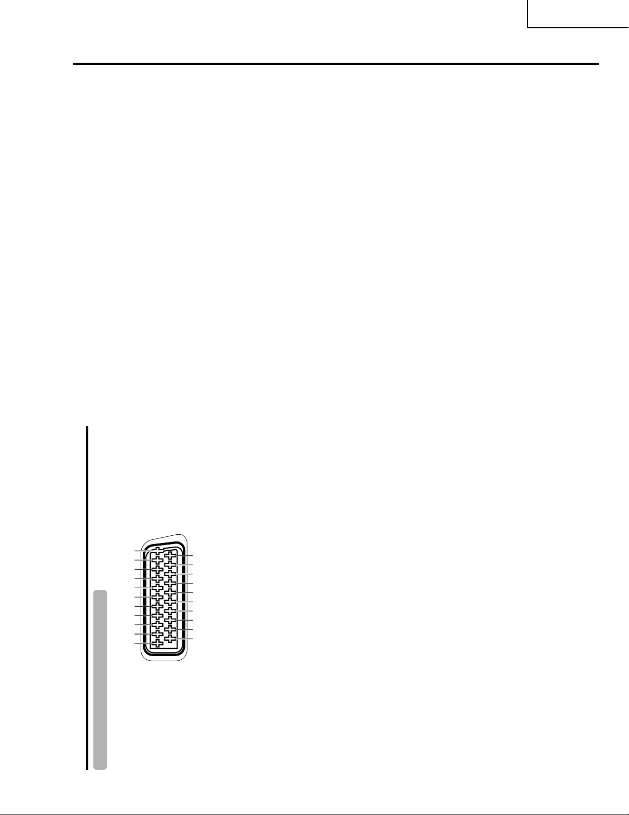
Various audio and video devices may be connected via the SCART terminals.
9
Page 10
LC-30HV2E
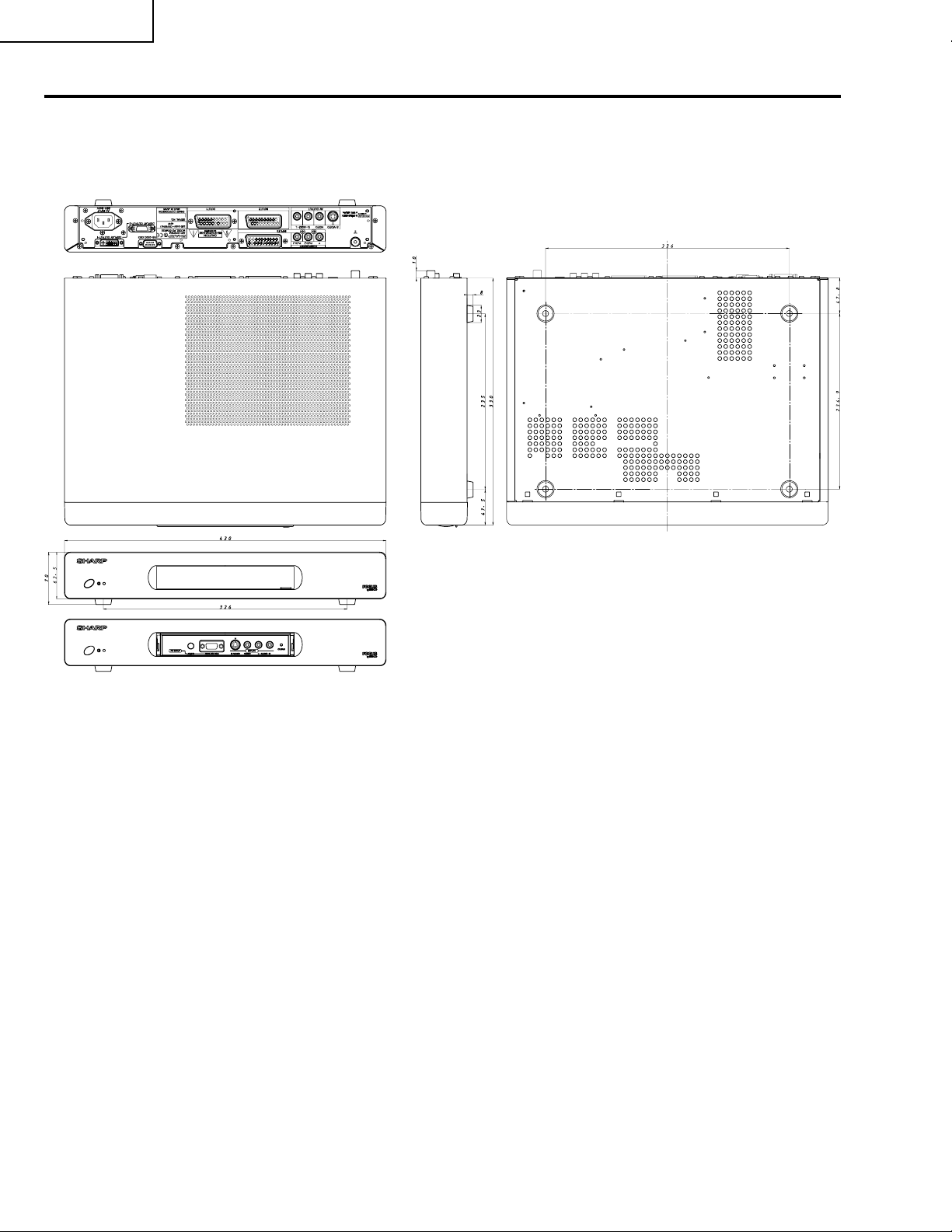
Dimensions
AVC
(Unit: mm)
10
Page 11
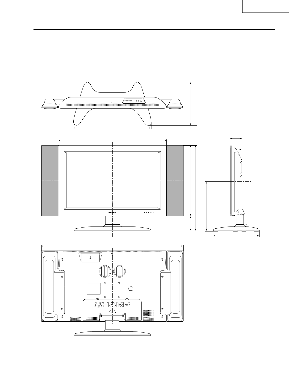
LCD
LC-30HV2E
Unit: mm
545
766.4
1002.4
84.5
497 304.5101
598
354
304.5
DISPLAY OUTPUT-2 DISPLAY OUTPUT-1
AC INPUT
110V–240V
11
Page 12
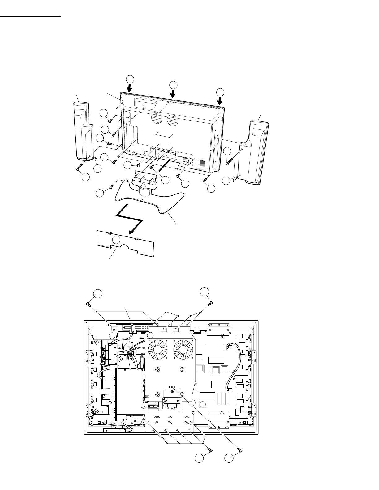
LC-30HV2E
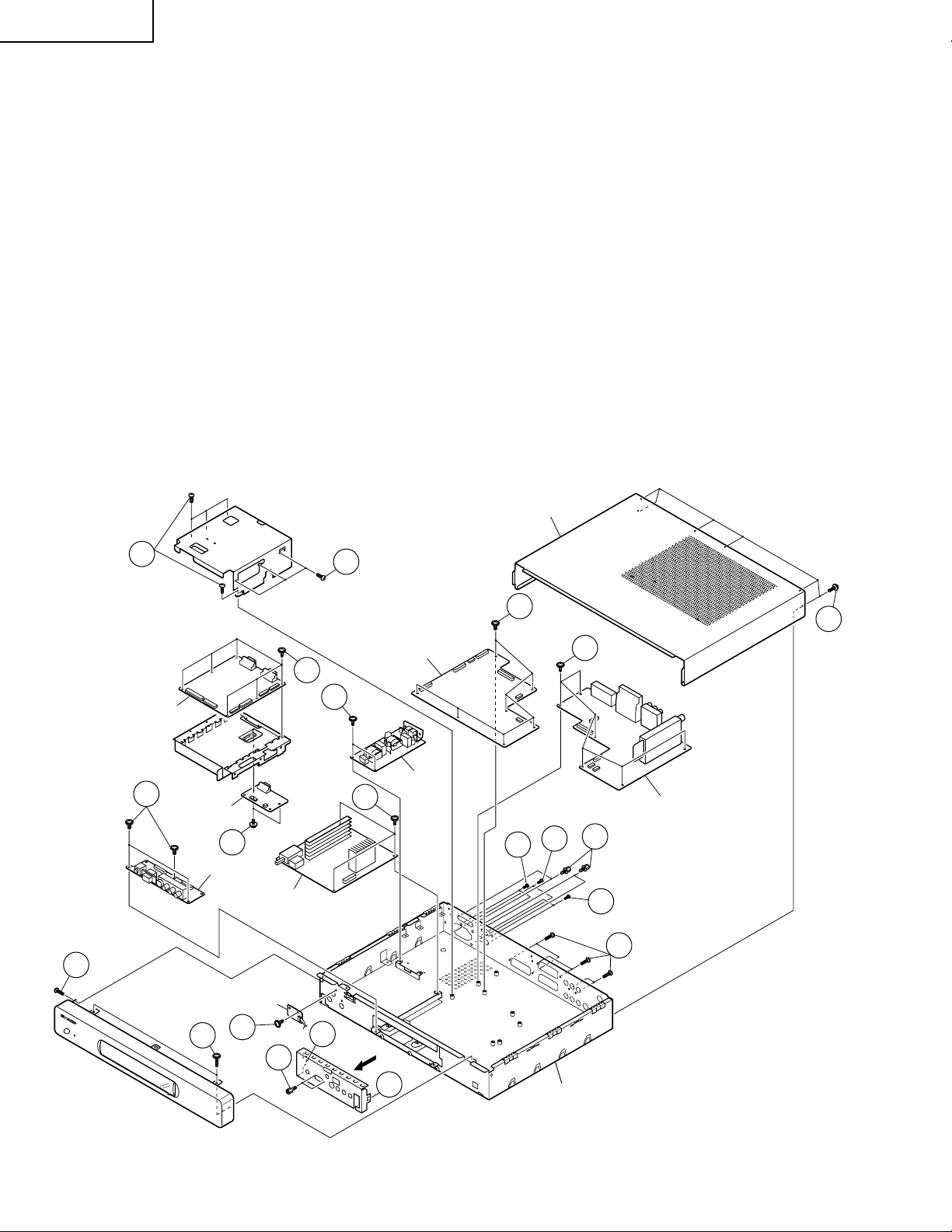
REMOVING OF MAJOR PARTS
AVC System
1. Remove the six lock screws from the back of the top cabinet. Slide the top cabinet backward and detach it.
2. Remove the three lock screws from the front panel. Undo the three hooks at the top and the four hooks at the
bottom, and detach the front panel.
3. Remove the two hexagonal shafts from the front shield. Undo the two hooks on both sides and detach the
front shield.
4. Remove the three lock screws from the front unit and detach this unit.
5. Remove the one lock screw from the LED unit and detach this unit.
6. Remove the PC I/F unit and SR unit assemblies.
6-1. Remove the two hexagonal shafts each from the system cable (white) terminal and the RS-232C terminal,
both on the PC I/F unit.
6-2. Remove two lock screws from the system cable (gray) terminal also on the SR unit.
6-3. Remove the two lock screws from the PC I/F unit bracket.
6-4. Remove the four lock screws from the PC I/F unit and SR unit assemblies. Take out these assemblies.
6-5. Remove the three lock screws from the brackets of the PC I/F unit and SR unit assemblies. Detach the
shield.
6-6. Remove the six lock screws from the PC I/F unit. Detach this unit from the bracket.
6-7. Remove the two lock screws from the SR unit. Detach this unit from the bracket.
7. Remove the seven lock screws from the main unit and detach this unit.
Top Cabinet
6-4
PC I/F Unit
4
SR Unit
6-7
Front Unit
Power Unit
2
6-6
9-2
6-5
10
Main Unit
EMC Unit
6-3
7
8-2
AV Unit
6-1
9-1
6-2
8-1
1
2
LED Unit
5
3
3
3
Bottom Cabinet
12
Page 13

8. Remove the AV unit.
8-1. Remove the six lock screws from the AV unit.
8-2. Remove the six lock screws from the AV unit and detach this unit.
9. Remove the EMC unit assemblies.
9-1. Remove the two lock screws from the EMC unit bracket.
9-2. Remove the two lock screws from the EMC unit and detach this unit.
10. Remove the three lock screws from the power unit and detach this unit.
LC-30HV2E
13
Page 14
LC-30HV2E
LCD Display
1. Take off bottom terminal cover.
2. Take off the speaker by removing 4 screws and disconnecting speaker terminals.
3. Take off the table stand by removing 6 screws.
4. Take off the rear cabinet by removing 20 screws and releasing the front cabinet's 6 hooks.
Speaker
4
Rear Cabinet
4
4
Speaker
2
4
4
4
4
2
3
1
Terminal Cover
2
4
4
Table Stand
4
2
4
5. Take off the operation cover assembly by removing 2 screws and detaching the connector.
6. Take off the center angle by removing 11 screws and disconnecting 1 lead wire from the fan.
5
Operation Cover Ass'y
5
P130
P308 P309
6
Center Angle
6
6
6
14
Page 15
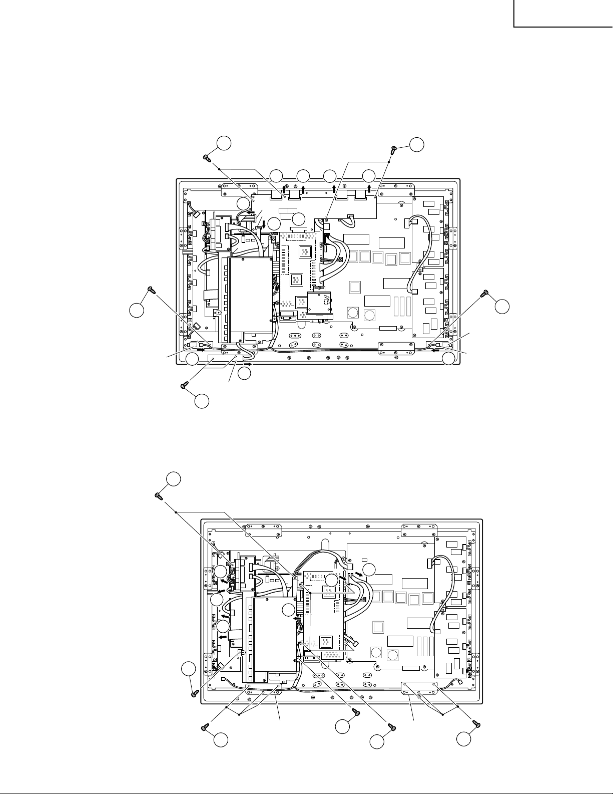
9. Take off the LED PWB by detaching one connector and removing 2 screws.
)
10.Take off the speaker (L) PWB by detaching one connector and removing one screw.
11.Take off the speaker (R) PWB by detaching one connector and removing one screw.
12.Take off the digital PWB by detaching one connector and removing 4 screws.
LC-30HV2E
12
12
P3503
SC4502
SC4551
SC4101
12
12
12
12
Digital
PWB
12
SC4503
12
12
10
P202
Speaker(L)
PWB
10
11
9
LEDPWB
9
13.Take off the main board by detaching 8 connectors and removing 4 screws.
14.Take off the SOUND PWB assembly by detaching 3 connectors and removing 4 screws.
15.Take off the 2 reinforcement angles by removing 3 screws from each angle.
Speaker(R
PWB
P201
11
14
14
14
14
14
15
P305
P430
P7001
Reinforcement angle
Sound
PWB
13
SC2401
Main
Board
13
CN4
14
CN3
13
13
Reinforcement angle
15
15
Page 16
LC-30HV2E
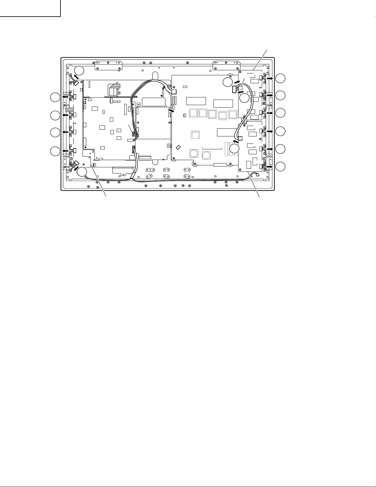
16.Detach each connector.
Inverter 1PWB
16
16
16
16
P601
P603
P605
P607
P609
16
P611
16
P305
Inverter
GND PWB
P3503
P301
P302
P4302
PC007
CN8
CN5
Power Unit
16
CN9
P65
16
P6564
16
Inverter 2 PWB
P6551
16
P6553
16
P6555
16
P6558
16
P6560
16
P6562
16
16
Page 17
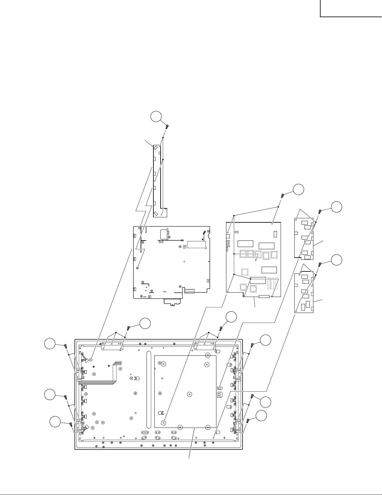
17.Take off the inverter GND PWB by removing 3 screws.
20.Take off the power PWB by removing 6 screws. Remove insulation sheet.
21.Take off the inverter 1 PWB by removing 3 screws.
22.Take off the inverter 2 PWB by removing 3 screws
23.Take off the 4 reinforcement angles by removing 2 screws from each angle.
24.Take off the 2 reinforcement angles by removing 3 screws from each angle.
25.Take off the LCD panel assembly by removing 2 screws.
17
Inverter GND
PWB
LC-30HV2E
23
20
21
Inverter 1 PWB
22
Inverter 2 PWB
Power Unit
24
24
23
23
23
25
25
Insulation Sheet
17
Page 18
LC-30HV2E
26.Take off the LCD panel with panel shield by removing 4 screws.
27.Take off D-BEF sheet, prism sheet and diffusion sheet. Take off ITO sheet and diffusion panel by removing 2
screws.
28.Take off the panel shield by removing 6 screws and 2 in the center.
26
LCD Panel
LCD Panel
27
26
28
Diffusion Sheet
Prism Sheet
D-BEF Sheet
28
27
27
Lamp
Panel Shield
28
Diffusion Panel
ITO Sheet
18
Page 19
ADJUSTMENT PROCEDURES
Ë
Procedure for turning ON the power
1. Connecting the system
» Using the system cable, connect the LCD Display Unit and the AVC System.
» Connect the LCD Display Unit to the AC power source.
» Connect the AVC System to the AC power source.
2. Procedure for turning ON the power
1 Press MAIN POWER on the Display.
•The STANDBY/ON indicator on the Display flashes red.
2 Press POWER on the AVC System.
•The System turns the power on.
•The STANDBY/ON indicator on the Display lights up green and the one on the AVC System lights up green.
•If the STANDBY/ON indicators still light up red, press B on the remote control unit or STANDBY/ON button on
the Display to turn the System on.
When turning the AVC System on first
1 Press POWER on the AVC System.
•The STANDBY/ON indicator on the AVC System lights up red.
2 Press MAIN POWER on the Display.
•The System turns the power on.
•The STANDBY/ON indicator on the Display lights up green and the one on the AVC System lights up green.
•If the STANDBY/ON indicators still light up red, press B on the remote control unit or STANDBY/ON button on
the Display to turn the System on.
LC-30HV2E
Display status indicator
Off
Flashing red
Red
Green
AVC System status indicator
Off
Red
Green
Ë
Procedure for upgrading the software (AVC System)
(1)With the power being OFF, open the top cabinet for the AVC System and then set the slide switch from the
NORMAL position to the WRITE position by inserting a needle-like insulator into the cutout located between
the WHITE port on the rear of the shield case for the PC I/F unit and the RS-232C port.
(2)Connect the PC having the program installed, to the AVC System using the cross cable for the RS-232C port
(for the details of the program, see Appendix).
(3)Open the MS-DOS window on the PC and then go to the directory in which the software is installed.
(4)Start up the system to which the AVC System and LCD Display Unit have been connected.
(5)Run “vup.bat (tentaive name)” at the MS-DOS prompt. The software will be upgraded.
(6)Load the file “civc_XXXXa.bhxmain.bhxosd.bhxt (tentaive name)”. It will take approximately a few minutes
until the file has been loaded. Never turn OFF the power or operate the system during this rewriting period.
(7)After the file has been loaded, turn OFF the LCD Display Unit and the AVC System and then return the slide
switch in the above step 1 from the WRITE position to the NORMAL position. Now the software has been
upgraded.
Power off
AVC System does not turn on or its AC cord is disconnected.
The System is in standby mode.
The System turns the power on.
Power off
Only the AVC System is in standby mode or the System is in standby mode.
The System turns the power on.
19
Page 20

LC-30HV2E
Ë
Procedure for adjusting each part of AVC System and LCD Display
» The adjustments were made to the best settings at factory. If any setting deviates or if any readjustment is
regarded as necessary when any part is replaced, perform the following steps.
» Any parameter that has been changed within the process adjustment is stored on the memory . If any readjustment
is required, write down the current value before changing it.
» Use a stable AC power source.
» If the program is upgraded, it will take approximately 1 minute for the EEPROM to be initialized before any video
appears. Therefore, you will need to wait for this time period. Do not turn OFF the power or operate the system
during the period.
» If the program is rewritten, write down the parameters that have been changed within the process adjustment
(see “5”.OSD menu and parameters displayed at manual adjustment), initialize the EEPROM, and then reenter
the recorded values.
1.
LCD display adjustment
See "Adjusting mode" for the steps to go into adjustment process mode.
1) +B adjustment (Digital PWB: R4648)
1. Receive PAL standard color bar.
2. Connect digital voltmeter to TP4602 and adjust to the specified value.
Specification: 13.00V ± 0.05V
2) Common bias adjustment
1. Go to "Adjustment process mode".
2. On the LCD, select "14" of "PATTERN 1", dot inversion flicker pattern 2.
3. Then, select "COM BIAS" on the LCD.
4. Set the value so that the flicker on the screen is minimized.
3) Background adjustment
1. Select video standard, and confirm the indication that the unit is preset to the standard.
2. At video input, receive the window pattern signal having left 80% WHITE and right 20% WHITE.
3. Set the screen size to the full mode.
4. Go to "Adjustment process mode".
5. Adjust "R OFFSET", "G OFFSET" and "B OFFSET" in "SIL861" so that right side 20% WHITE window pattern is
set to the specified value.
Specification: x = 0.294 y = 0.293 (80% WHITE) = 0.266 y = 0.253 (20% WHITE) [Minolta CA-110 No. 42941022]
4) Initialization
1. Go to "Adjustment process mode".
2. Select "1" thru "3" of "CLR MODE" in "TEST".
Setting range: 0 Normal
1 Initial setting (User clear: Factory setting)
2 Initial setting (All clear) Full initialization of EEPROM (except for ROM area)
3 Full initialization of Configuration EEPROM
3. Move the cursor down by one line.
4. Press "VOL UP" key and change the display from "WAIT" to "SEND" (write).
5. Do not shut down power while the display is "SEND".
6. When the writing is finished, the display changes from "SEND" to "WAIT".
20
Page 21

5) Resetting lamp error counter
1. Go to "Adjustment process mode".
2. Select "L ERR RESET" in "TEST".
3. Reset the data to "0".
[L ERR RESET]
Function: Reset of fluorescent lamp error counter
It resets the times of fluorescent lamp errors and clears the last value in the memory.
Indication range: 0-5 (Fluorescent lamp errors)
(When lamp error exceeds 5 times, power supply is disabled. Resetting is required in this case.)
LC-30HV2E
21
Page 22

LC-30HV2E
2.
Special Mode
1. Entering a special mode
1 Entering the process adjustment mode
[Steps]
(1)When using the remote control unit:
Using the system cable, properly connect the LCD Display Unit and the AVC System, and then turn ON
the power.
After the system has started up, press the PROCESS ADJ button located on the remote control unit.
(2)When using buttons on the main unit:
Using the system cable, properly connect the LCD Display Unit and the AVC System.
Turn ON the power while holding down the INPUT and CH UP buttons located the LCD Display Unit.
[Description]
Various adjustments can be made manually.
2 Entering the inspection process mode
[Steps]
After the system has started up, press the PROCESS ADJ button located on the remote control unit.
Set the parameter SIGNAL INFO to 1 on page 6 or 7 of the PROCESS ADJUSTMENT A MODE MENU.
Subsequently, make the necessary adjustments in accordance with the above menu.
3 Procedure for setting up delivery
[Steps]
After the system has started up, press the DELIVERY SETUP button located on the remote control unit.
(Within the adjustment process, the channel settings remain unchanged. Once you exit the process adjustment
mode, the channel settings entered in the delivery adjustment mode become valid.)
[Description]
The user’s adjustment parameters and others will be set to the default values. The channel settings will also
be initialized.
2. Exiting a special mode
(1)Process adjustment mode: Press the PROCESS ADJ button located on the remote control unit or turn OFF the
power.
(2)Inspection process mode: Set the parameter SIGNAL INFO to 0 on page 6 or 7 of the PROCESS ADJ A MODE
MENU or turn OFF the power.
(3)Delivery setup: After the delivery setup has been finished, the process adjustment mode is automatically
selected. To exit the process adjustment mode, press the PROCESS ADJ button located on the remote control
unit or turn OFF the power.
3. OSD menu and parameters displayed at manual adjustment
* The default values may slightly differ depending upon the program version to be rewritten.
* The settings are not initialized to the default values by merely rewriting the program. (See the paragraph for
Preparation for adjustment.)
(1)Descriptions of special buttons in process adjustment mode
Cursor UP key : Proceeds to the previous page.
Cursor DOWN key: Returns to the next page.
VOL UP key : Increases the adjusted value by 1.
VOL DOWN key : Decreases the adjusted value by 1.
Cursor LEFT key : Decreases the adjusted value by 10.
Cursor RIGHT key : Increases the adjusted value by 10.
CH UP key : Moves up the cursor.
CH DOWN key : Moves down the cursor.
22
Page 23
Ë
Maker Select
Ë +Badj3.3V
Ë +Badj2.5V
KEY WRITE
Ë DATA COPY
INDUSTRY INIT
CENTER Version
OSD Version
CVIC Version
TTXP V ersion
MONITOR Version
PANEL Version
FLASH Version
MONITOR Model
Model Select MONITOR
STANDBY TYPE
SHARP
127
024
OFF
OFF
OFF
MR MAIN E 2001/11/28K
MR OSD 2001/09/10 A
W2001/10/02 17:28 X2001/10/02 V2001/09/12 09:12
TTX PRG 068
F6 91 xx
-00
-05
01
1
0
Page Input Source HDCP
INPUT1 No SIG1/16 HDCP:ON EUROPE EUROPE
Destination for MAIN unit Destination for AV unitDistinguish Signal
Organization of process adjustment screen
LC-30HV2E
Parameter display
Ë
+B Adj3.3V
Ë
+B Adj2.5V
Ë
P AL Y CONTRAST
Ë
PAL COLOR GAIN
Ë
MAIN CR GAIN PAL
Ë
MAIN SUBBRIGHT 15K
Ë
MAIN CONTRAST 15K
Ë
SUB P AL Y
Ë
SUB PAL COLOR GAIN
Ë
PEAK ACL SW
Ë
SECAM Y CONTRAST
Ë
SECAM COLOR GAIN
Ë
MAIN CR GAIN SECAM
Ë
N358 Y CONTRAST
Ë
N358 COLOR GAIN
Ë
MAIN CR GAIN N358
Ë
N358 TINT
Ë
COMP 15K Y CONTRAST
Ë
COMP 15K COLOR GAIN
Ë
MAIN CR GAIN COMP15K
Ë
COMP HDTV SUB BRIGHT
Ë
COMP HDTV CONTRAST
Ë
DA TA COPY
The values for the above parameters should be written down before the EEPROM is replaced on
the AVC system.
Note: The contents on the adjustment process menu may be somewhat different depending on
the program's version-ip.
Setting range
0 ~ 255
0 ~ 255
0~ 63
0~ 63
0 ~ 255
0~ 63
0~ 15
-30 ~ 30
0~ 63
OFF/ON
0~ 63
0~ 63
0 ~ 255
0~ 63
0~ 63
0 ~ 255
-30 ~ 30
0~ 63
0~ 68
0 ~ 255
0~ 63
0~ 15
OFF/ON
Description
3.3 V adjustment
2.2 V adjustment
P AL Y level adjustment
PAL colour density adjustment
PAL Cr level adjustment
Pedestal level adjustment (15 k)
PCB input amplitude adjustment (15 k)
Sub P AL Y level adjustment
Sub PAL colour density adjustment
SECAM Y level adjustment
SECAM colour density level adjustment
SECAM Cr level adjustment
N358 Y level adjustment
N358 colour density adjustment
N358 Cr level adjustment
N358 tone adjustment
COMP 15 k Y level adjustment
COMP 15 k colour density adjustment
COMP 15 k Cr level adjustment
COMP HDTV black level adjustment
COMP HDTV Y level adjustment
COMP HDTV colour density adjustment
23
Page 24
LC-30HV2E
0.35V
0.35V
4. Procedures before and after replacing the PC I/F unit
1) Before replacing the PC I/F unit, write down the values for the parameters listed on the 2nd and 3rd pages of
the Adjustment Process A screen.
If the values for the parameters cannot be written down because the PC I/F unit is completely broken or for any
other reason, make all the adjustments in accordance with the paragraph for Adjustment procedure and
parameters, rather than the following procedures. (End)
Set the parameters listed on the 2nd and 3rd pages of the Adjustment Process A screen to the values you have
written down.
5. Adjustment parameters
1) Analog adjustment
(1) Prior adjustment for AVC system chassis
Adjustment item Description Adjustment procedure
1 Destination check 1. Call the process adjustment mode.
2. Check that the destination is “Europe”.
2 AVC center 3.3V
adjustment
3 AVC center 2.5V
adjustment
Connect DC voltmeter to
TP1702.
Connect DC voltmeter to
TP1701.
Adjust output voltage of DC/DC 5 V line to
3.3 V .
Adjusted value: 3.25~3.29 V
Adjust output voltage of DC/DC 2.5 V line to
2.6 V .
Adjusted value: 2.60~2.64 V
(2) PAL signal adjustment
Adjustment item Description Adjustment procedure
1 Setup 1. Set colour system to “PAL”.
2. Select PAL source.
100% colour bar signal including 100% white, such
as split field colour bar
2 Tuner Y level
adjustment
3 PAL Y CONTRAST
adjustment
4 PAL COLOR GAIN
adjustment
1. Adjust TP1101 so that the Y signal without the
chroma component should be 1.00 ±0.05 Vp-p
(between the bottom of sync signal and the white
peak).
1. Adjust TB1274_MAIN output (TP803) to
0.7 ±0.05 Vp-p.
1. Adjust TB1274_MAIN
output (TP802) to
0.35 ±0.025 Vp-p.
5 MAIN CR GAIN PAL
adjustment
6 MAIN CONTRAST
adjustment
Press the DUAL screen button. 1. Select the special DUAL screen settings for
7 SUB PAL Y adjustment 1. Adjust TB1274_SUB output (TP806) to
8 SUB PAL COLOR
GAIN adjustment
1. Adjust TB1274_MAIN output
(TP801) to 0.35 ±0.05 Vp-p.
1. Turn off the PEAK ACL control. Adjust the output
(TP815) of IC810 to have 1.1 ±0.05 Vp-p from the
pedestal level.
adjustment (so that the same video source is
reflected on MAIN/SUB).
0.9 ±0.05 Vp-p.
1. Adjust TB1274_SUB output (TP805) to
0.9 ±0.05 Vp-p.
24
Page 25
(3) SECAM signal adjustment
Adjustment item Description Adjustment procedure
1 Setup 1. Set colour system to SECAM.
2. Select SECAM source.
100% colour bar signal including 100% white, such
as split field colour bar
2 SECAM Y CONTRAST
adjustment
3 SECAM COLOR GAIN
adjustment
1. Adjust TB1274_MAIN output (TP803) to
0.7 ±0.05 Vp-p.
1. Adjust TB1274_MAIN
output (TP802) to 0.35
±0.025 Vp-p.
LC-30HV2E
0.35V
4 MAIN CR GAIN
SECAM adjustment
1. Adjust TB1274_MAIN
output (TP801) to 0.35
±0.025 Vp-p.
(4) N358 signal adjustment
Adjustment item Description Adjustment procedure
1 Setup 1. Set colour system to N358.
2. Select N358 source.
100% SMPTE colour bar or similar colour bar
signal including 100% white.
2 N358 Y CONTRAST
adjustment
3 N358 COLOR GAIN
adjustment
4 MAIN CR GAIN N358
adjustment
1. Adjust TB1274_MAIN output (TP803) to
0.7 ±0.05 Vp-p.
1. Adjust TB1274_MAIN
output (TP802) to 0.35
±0.025 Vp-p.
1. Adjust TB1274_MAIN
output (TP801) to 0.35
±0.025 Vp-p.
0.35V
0.35V
0.35V
5 N358 TINT adjustment 1. Adjust TB1274_MAIN output (TP802) so that
waveform becomes as illustrated below:
Smoothed
25
Page 26
LC-30HV2E
0.35V
0.35V
(5) Component 15k Hz signal adjustment
Adjustment item Description Adjustment procedure
1 Setup 1. Select component 15k Hz.
2. Select component source.
100% colour bar signal including 100% white, like
split field colour bar
2 COMP 15k
CONTRAST
adjustment
3 COMP 15k COLOR
GAIN adjustment
Adjust TB1274_MAIN output (TP803) to 0.7 ±0.05 Vp-p.
Adjust TB1274_MAIN output
(TP802) to 0.35 ±0.025 Vp-p.
4 MAIN CR GAIN COMP
15k adjustment
Adjust TB1274_MAIN output
(TP801) to 0.35 ±0.025 Vp-p.
(6) Component HDTV signal adjustment
Adjustment item Description Adjustment procedure
1 Setup 1. Input HDTV (1080i) component signal.
2. Select component source.
100% colour bar signal including 100% white, like
split field colour bar
2 COMP HDTV
CONTRAST
adjustment
Turn off the PEAK ACL control.
Adjust the output (TP815) of pin (11) of IC810 to have
1.1 ±0.05 Vp-p from the pedestal level.
2. Factory settings
(1) Data Copy
Adjustment item Description Adjustment procedure
1 DATA COPY 1. Using the adjustment key, set “ON” in the DATA
COPY line. Wait until “OFF” is displayed instead.
Finally turn off the power to quit the process
adjustment mode.
(2) Delivery setup
Adjustment item Description Adjustment procedure
1 DELIVERY SETUP Press the Delivery Setup button located on the remote
control unit, or position the cursor on the INDUSTRY
INIT line, set the line to ON with the ADJ key, and then
press the ENTER key. The adjustment is finished
when the line turns OFF,
* Finally press the process adjustment key on the remote control unit to exit from the process adjustment mode. Then turn off
the AC power supply of the AVC system. (Be careful not to use the power switches of the remote control unit and AVC system.)
26
Page 27
LC-30HV2E
3.
Adjusting Mode
1. Overview
The controller IC can be adjusted in this mode.
Adjustment is done while controlling the setting of the resistor corresponding to the selected adjustment item.
When monitor is used independently, it is adjusted using the OSD simple display function incorporated in LCD
controller.
The OSD function of panel link receiver (SIL861) is used for adjustment of the independent monitor.
2. Entry to the mode
1) When cable is not connected (independent mode), follow the steps below.
a) When power switch is turned on, press the main unit INPUT and VOL DOWN keys simultaneously.
b) Press the remote controller's process adjustment key (R/C code: 40h) / process adjustment mode 2 key (R/
C code: 31h).
2) When not in independent mode, follow the steps below.
a) When power switch is turned on, press the main unit CH DOWN and VOL UP keys simultaneously.
b) Press the remote controller's process adjustment mode 2 key.
3. Exit from the mode
Turn off the power.
Press the remote controller's process adjustment mode 2 key.
4. Display
1) First layer display
The third line shows the title. The 5th line and below show the items. Microprocessor's version number
appears in the 16th line.
Example) 1.00 ) 1 00
1234567891011121314
1SERVICE MODE
2OMODE 50HZ
3LCD
4SIL861
5TEST
6VERXXX
2) Second layer display (Adjustment item display)
A single page shows up to 10 adjustment items (or 14 lines).
The third line shows the title and the screen mode selected in MODE items (only when LCD is selected).
The 5th line shows the item. Microprocessor's version number appears in the 16th line.
Example) 1.00 ) 1 00
Setting is shown in decimal number.
a) Adjustment on the LCD items
1234567891011121314
1LCD 50HZ
2OVL0 22 1
3REF0 209
4VL64 98
5REF64 170
6VL96 92
7REF96 184
8 VL128 85
9REF128 188
10 VL160 71
11 REF160 199
27
Page 28
LC-30HV2E
b) Adjustment on the TEST items
1234567891011121314
1TEST
2OL ERR RE 0
3LCDDATA0000
4WAIT
5CLRMODE 0
6WAIT
7 CNFG EEP 000 0
8WAIT
5. Changing data
In "adjustment item display", the items pointed by cursor can be changed using VOL UP/DOWN key.(Holding
down the key is effective.)
For the items in "LCD DATA", select the item and hit ENTER key. The ten's digit (leftmost digit) in the address
changes to red (others in green). Data change using VOL UP/DOWN key is enabled.
To move to the next digit, press CH UP key (or rightward cursor key). To go back to the previous digit, press CH
DOWN key (or leftward cursor key). Thus, 4 digits data can be entered.
When CH UP key is pressed while in rightmost digit, the cursor moves to the leftmost digit. When CH DOWN
key is pressed while in leftmost digit, the cursor moves to the rightmost digit.
After address data adjustment, press ENTER key to exit from 4-digit adjustment and change the entire "LCD
DATA" line to red letters. (Same status as item selection)
6. Key operation
1) Basic behaviors
Basic key behaviors are as follows.
Behavior Keys
Remote controller Main unit
Upward cursor movement Cursor up CH UP
Downward cursor movement Cursor down CH DOWN
Rightward cursor movement Cursor right
Leftward cursor movement Cursor left
Data UP VOL UP VOL UP
Data DOWN VOL DOWN VOL DOWN
Set ENTER INPUT
Back to previous layer RETURN
Back (In bottom layer only) ENTER INPUT
2) Data UP/DOWN
For the item for which OSD display is available, switch the display.
Adjust the data with UP/DOWN operation. (Any value beyond the limit is replaced by the limit value.)
Output data processing
Data transmission for every UP/DOWN operation (Data related to peripheral controller IC)
Execution of the last memory data when key is off
While the key is held down, the second step is performed approx. 500ms after the key operation and, after this,
every single step of UP/DOWN is carried out sequentially at 135ms interval.
3) Cursor UP/DOWN
Select the adjustment item by pointing it with the cursor.
When upward cursor movement is done while the cursor is at the top item, the cursor goes to the bottom item.
(In the case of multiple pages, the cursor goes to the bottom item on the previous page.)
When downward cursor movement is done while the cursor is at the bottom item, the cursor goes to the top
item. (In the case of multiple pages, the cursor goes to the top item on the next page.)
While the key is held down, the second step is performed approx. 500ms after the key operation and, after this,
every single step of UP/DOWN is carried out sequentially at 135ms interval.
28
Page 29
ADJUSTMENT MODE MENU LIST
First layer item PAGE ITEM SETTING RANGE INITIAL VALUE DATA SETTING
MODE 1 50HZ/60HZ/PC 50HZ Toggle
LCD 1 VL0 0 ~ 255 221 No Toggle
REF0 0 ~ 255 209 No Toggle
VL64 0 ~ 255 98 No Toggle
REF64 0 ~ 255 170 No Toggle
VL96 0 ~ 255 92 No Toggle
REF96 0 ~ 255 184 No Toggle
VL128 0 ~ 255 85 No Toggle
REF128 0 ~ 255 188 No Toggle
VL160 0 ~ 255 71 No Toggle
REF160 0 ~ 255 199 No Toggle
2 VL192 0 ~ 255 77 No Toggle
REF192 0 ~ 255 103 No Toggle
VL224 0 ~ 255 88 No Toggle
REF224 0 ~ 255 112 No Toggle
VL256 0 ~ 255 108 No Toggle
REF256 0 ~ 255 78 No Toggle
COM BIAS 0 ~ 255 70 No Toggle
PWM CTRL 0 ~ 7 Toggle
PWM FREQ 0 ~ 4095 585 No Toggle
PWM DUTY 0 ~ 4095 0 No Toggle
3 PATTERN1 0 ~ 14 0 Toggle
PATTERN2 0 ~ 12 0 Toggle
P – CLK1 0 ~ 3 0 No Toggle
P – CLK2 0 ~ 7 0 No Toggle
OS SW 0 ~ 1 0 Toggle
OS D1 0 ~ 255 138 No Toggle
OS D2 0 ~ 255 167 No Toggle
OS D3 0 ~ 255 170 No Toggle
OPC LV0 0 ~ 85 0(40) No Toggle
OPC LV1 0 ~ 85 8(44) No Toggle
4 OPC LV2 0 ~ 85 16(48) No Toggle
OPC LV3 0 ~ 85 24(52 )No Toggle
OPC LV4 0 ~ 85 32(56) No Toggle
OPC LV5 0 ~ 85 40(60) No Toggle
OPC LV6 0 ~ 85 48(64) No Toggle
OPC LV7 0 ~ 85 56(68) No Toggle
OPC LV8 0 ~ 85 64(72) No Toggle
OPC LV9 0 ~ 85 72(76) No Toggle
OPC LV10 0 ~ 85 80(80) No Toggle
SIL861 1 R GAMMA 20 ~ 180 100 No Toggle
R OFFSET 0 ~ 510 256 No Toggle
G GAMMA 20 ~ 180 100 No Toggle
G OFFSET 0 ~ 510 256 No Toggle
B GAMMA 20 ~ 180 100 No Toggle
B OFFSET 0 ~ 510 256 No Toggle
TEST 1 L ERR RESET 0 ~ 5 0 Toggle
LCD DATA Four digits 0 ~ F 0 Toggle
WAIT/SEND WAIT ———
CLR MODE One digits 0 ~ 2 0 Toggle
WAIT/SEND WAIT ———
CNFG EEP Four digits 0 ~ F 0 Toggle
WAIT/SEND WAIT ———
LC-30HV2E
* Values in the parentheses are with PC.
29
Page 30

LC-30HV2E
DESCRIPTION OF MAJOR IC FUNCTIONS
Æ Description of Main ICs
»»
» IC1301 (CXA2069Q)
»»
This IC is a 7-input, 3-output selector.
The video signals other than those for the PC, components and RGB input, which have been input from each input
connector and the tuner, and all the audio signals are sent to the IC1301 and then selected.
Output 1 is used internally and output 3 in the monitor output.
When the S video input is output to the monitor, Y and C signals are mixed in this IC.
The video signals sent to the IC1301 are then input to the YC separation circuits, IC405 (main) and IC402 (sub).
The audio signals are input to the PC I/F Unit via IC2501 (sound processor).
»»
» IC1401 (MM1519XQ)
»»
This IC is a 4-input, 8-output video selector for component input.
The AV3 component input, AV1, RGB input, and Teletext RGB signals are input to the IC1401. The output signals
go to the main, sub, and component channels.
»»
» IC1601 (SDA5550M).
»»
This IC is a microprocessor for Teletext.
Video signals are input to the IC1601, which then decodes the Teletex data and outputs it as RGB data.
»»
» IC2501 (IX3371CE)
»»
This IC is used to decode audio signals.
It serves as both the S IF decoder and the selector for the input audio data.
»»
» IC801/IC802 (TB1274AF)
»»
This IC synchronizes video and chroma signals for PAL/NTSC/SECAM colour televisions.
Its video circuit includes a high-performance image quality compensation circuit and its chroma circuit a PAL/
NTSC/SECAM automatic selection circuit. The P AL-M/N clock signals at 4.43 and 8.58 MHz are internally generated
for colour demodulation.
The PAL/SECAM demodulation circuit uses a base band signal processing system with built-in IH DL and is
therefore adjustment-free.
The IC801/IC802 has 4 lines for YC signal input, 2 lines for RGB signal input, and 2 lines for colour difference
signal input. It receives colour different signals for the main and sub channels from IC405 (main), IC402 (sub), and
IC1401 in the former stage, and provides 1 line for colour difference signal output.
»»
» IC803 (CXA2101Q)
»»
This IC consists of a base band signal processing section for colour different input, an RGB signal processing
section, and a 4-line video switch (including HV synchronizing signal processing).
Input selection is performed by INPUT-SEL (I2C BUS). YCbCr , HD YPbPr , GBR and their respective HV synchronizing
signals are input to each line.
As the multi-scanning compliance range, a horizontal scanning frequency of 15~60 kHz can be input.
»»
» IC1901 (IX3566CE)
»»
This IC is FPGA for the synchronizing system.
It creates sand castle pulses for IC803 and generates horizontal blanking signals.
»»
» IC604 (TA1318AF)
»»
This IC synchronizes TV component signals.
The IC804 incorporates the necessary functions for measuring the frequency of input signals and synchronous
replay into a single chip, and is applicable for horizontal synchronous replay (15.75, 31.5, 33.75, and 45 kHz) and
vertical synchronous replay (525I, 525P, 625I, 750P, 1125I, 1125P, PAL 100 Hz, and NTSC 120 Hz).
30
Page 31

LC-30HV2E
»»
» IC405/IC402 (CXD2064Q)
»»
This IC is a comb filter in the applicable field for both the NTSC and PAL systems. It performs the Y/C separation
of the main and sub channel video signals that have been output from IC1801.
»»
» IC407/IC404 (ML6428C1)
»»
This IC is a 6.7 MHz low-pass filter.
»»
» IC810/IC804 (IX3473CE)
»»
This IC is a 6.7 MHz low-pass filter incorporating a 6 dB amplifier.
»»
» IC811 (IX3474CE)
»»
This IC is a 30 MHz low-pass filter incorporating a 6 dB amplifier.
Æ Description of Functions of Main ICs on PC I/F Unit
»»
» IC4 (CXA3506R)
»»
This IC is an A/D converter that incorporates a 3-channel, 8-bit, 120 MSPS amplifier and PLL. It is used for the
video signals input to the PC I/F unit on the main channel in the 1-screen and 2-screen modes, and also for the
video signals input from the front for the PC.
The video signals (analog RGB) from the CN6 are input to IN1 of IC4.
For the PC, the video signals (analog RGB) from CN8 are input to IN2 of IC4.
The input video signals are converted into digital signals and then sent to IC25.
»»
» IC310 (TLC5733A)
»»
This IC is a 3-channel, 8-bit, 20 MSPS A/D converter.
It is used for the sub-channel of the video signals input to the PC I/F Unit in the 2-screen mode.
The video signals (analog Y, Cb, Cr) from CN6 are input to IC310.
The video signals input to this IC are converted into digital signals and then sent to IC25.
»»
» IC25 (IX3434CE)
»»
This IC performs the I/P conversion and scaling to match the digitalized video with the output resolution, and also
the data conversion.
It has two input lines, V0 and V1. The V0 line is used to process the RGB, composite, and skirt signals input to the
480i and 580i components for the sub-channel in the 2-screen mode. The V1 line is used to process all the signals
as well as V1 for the main channel in the 1-screen and 2-screen modes.
The IC25 detects what resolution is input from the input synchronizing signal; creates H synchronization in
accordance with the frequency division ratio; creates the clamp signal in accordance with the input synchronizing
signal; and performs the data matrix conversion.
The video signals input to this IC is sent to IC413.
»»
» IC413 (SiI168)
»»
This IC is a panel link transmitter.
It converts the 8-bit RGB video data output from IC25 into the differential TMDS signals and then digitally transmits
the converted signals to the monitor.
The TMDS signals are transmitted at the frequency 10 times higher than the clock frequency.
»»
» IC1 (IX3270CE)
»»
This IC is a 1-chip RISC microprocessor.
It performs communication with the monitor and operates the system.
The IC1 also controls each IC in the AVC system and partially manages the power source.
»»
» IC405 (uPD4721)
»»
This IC is an RS-232 line driver receiver conforming to the EIA/TIA-232-E standard.
The IC405, when connected to a PC, allows for externally controlling the system.
It is also applicable for upgrading IC1.
31
Page 32

LC-30HV2E
» The information shown in the list is basic information and may not correspond exactly to that shown in the schematic diagrams.
Ë VHiCXA2069Q-1 (ASSY: IC1301)
» S2-Compatible, 7-Input/3-Ouput AV Switch
» Block Diagram
32
Page 33

» Pin Function
Pin No. Pin Name I/O Pin Function
63
1
8
15
22
30
60
3
10
17
24
49
5
12
19
26
51
62, 2
9, 16
23, 29
59, 64
4, 11
18, 25
31, 61
53
41
44
56
39
58
47
37
52
43
38
54
45
40
6
13
20
27
7
14
21
28
32
33
34
36
55
46
48
50
TV
V1
V2
V3
V4
V5
V6
Y1
Y2
Y3
Y4
YIN1
C1
C2
C3
C4
CIN1
LTV, LV1
L V2, LV3
L V4, LV5
L V6, RTV
RV1, RV2
RV3, RV4
RV5, RV6
VOUT1
VOUT3
V/YOUT2
YOUT1
YOUT3
COUT1
COUT2
COUT3
LOUT1
LOUT2
LOUT3
ROUT1
ROUT2
ROUT3
S2-1
S2-2
S2-3
S2-4
S-1
S-2
S-3
S-4
ADR
SCL
SDA
DC OUT
TRAP1
TRAP2
MUTE
BIAS
I
I
I
I
I
I
I
I
I
I
I
I
I
I
I
I
I
I
I
I
I
I
I
I
O
O
O
O
O
O
O
O
O
O
O
O
O
O
I
I
I
I
I
I
I
I
I
I
I
O
I
I
I
I
Video signal input.
Composite video signal input
Y/C-separated signal input terminal for luminance signal input.
YIN1 to feed in the Y/C-separated signal of VOUT1 output.
Y/C-separated signal input terminal for chrominance signal input.
CIN1 to feed in the Y/C-separated signal of VOUT1 output.
Audio signal input terminal.
Video signal output terminal for composite video signal output.
Video signal output terminal for selection between composite video signal output and
luminance signal output by I2C Bus control.
Video signal output terminal for luminance signal output.
Video signal output terminal for chrominance signal output.
Audio signal output terminal.
Used to detect C signal-superimposed, S2-compatible DC level. 4:3 video signal when
below 1.3V. 4:3 letterbox signal when between 1.3V and 2.5V. 16:9 image squeeze
signal when above 2.5V. To be pulled down to GDN at 100KΩ to produce 4:3 video
signal when open.
Used to switch between composite video and S signals. Detection results to be written
in status register. S signal when below 3.5V. Composite video signal when above 3.5V.
To be pulled up to 5V at 100KΩ to produce composite video signal when open.
Used to select I2C Bus slave address. 90H when below 1.5V. 92H when above 2.5V.
90H also when the terminal is open.
I2C Bus signal input terminal.
I2C Bus signal input terminal.
Used to feed out S2-compatible DC level to be superimposed on COUT3 output. DC to
be superimposed by connecting to COUT3 output via a capacitor. Control to be made
by I2C Bus. S2-specified output impedance of 10 ±3KΩ to be realized by adding an
external resistance of 4.7KΩ.
Subcarrier trap circuit to be connected.
Audio signal output mute terminal. Mute off when below 1.3V. Mute on when above
2.5V. Mute off when the terminal is open.
Internal reference bias (Vcc/2) terminal. To be connected to GND with a capacitor in
between.
LC-30HV2E
33
Page 34

LC-30HV2E
Ë VHiMM1519XQ-1(IC1401)
» Component Input Video Switch
» Block Diagram
34
Page 35

» Pin Function
Pin No. Pin Name I/O Pin Function
1
2
3
11
12
13
21
22
23
4, 14, 39, 45, 52,
58
51
5
15
53
59
24
6, 8, 16, 18, 33,
35, 37, 41, 43, 47,
49, 54, 56, 60, 62
7
9
17
19
55
57
61
63
10
20
32
64
25
26
27
28
29
30
31
34
36
38
40
42
44
46
48
50
VIDEO 1-L1
VIDEO 1-L2
VIDEO 1-L3
VIDEO 2-L1
VIDEO 2-L2
VIDEO 2-L3
VIDEO 3-L1
VIDEO 3-L2
VIDEO 3-L3
VCC
AVCC
VIDEO 2-Y
VIDEO 3-Y
TUNER-Y
VIDEO 1-Y
DGND
GND
VIDEO 2-Pb
VIDEO 2-Pr
VIDEO 3-Pb
VIDEO 3-Pr
TUNER-Pb
TUNER-Pr
VIDEO 1-Pb
VIDEO 1-Pr
VIDEO 2-SW
VIDEO 3-SW
MONO-SW
VIDEO 1-SW
ADDRESS
SDA
SCL
DVCC
L3 OUT
L2 OUT
L1 OUT
Pr OUT 3
Pb OUT 3
Y OUT 3
Pr OUT 2
Pb OUT 2
Y OUT 2
Pr OUT 1
Pb OUT 1
Y OUT 1
—
—
—
—
I/O
—
O
O
O
O
O
O
O
O
O
O
O
O
I
I
I
I
I
I
I
I
I
I
I
I
I
I
I
I
I
I
I
I
I
I
I
I
I
I
I
Line input of D-terminal
Analog power supply (9V)
Y -signal input
GND
Pb, Pr signal input
Switch line of D-terminal
Slave address select pin
Data input of I2C bus
Clock input of I2C bus
Digital power supply (5V)
Line output for monitor
Video signal output
LC-30HV2E
35
Page 36

LC-30HV2E
Ë VHiSDA5550M-1 (ASSY: IC1601)
» Stereo Audio DAC
» Block Diagram
» Pin Function
Pin No. Pin Name I/O Pin Function
99, 1, 3, 4, 2, 100,
98, 96
97, 94, 93, 89, 86,
84, 82, 79, 81, 83,
90, 85, 77, 78, 76,
71, 69
70, 68, 67
9, 10, 11, 12, 13,
14, 15, 16
41, 42, 43, 44, 45,
46, 47, 62
24, 25, 26, 27
D0-D7
A0-A16
A17-A19/
P4.0, P4.1, P4.4
P0.0-P0.7
P1.0-P1.7
(PWM)
P2.0-P2.3
(ADC)
I/O
O
I/O
I/O
I/O
Data bus for external memory or data RAM.
Address bus for external program memory or data RAM.
After power-on P4.0,P4.1,P4.4 work as additional address lines A17…A19.
In port mode, these port lines act as bi-directional I/O port with internal pull-up
resistors. Port pins that have ‘1’ written to them are pulled high by the internal pull-up
resistors and in that state can be used as inputs.
Port 0 is a 8-bit open drain bi-directional I/O-port. Port 0 pins that have 1 written to
them float: in this state they can be used as high impedance inputs.
Port is a 8-bit bi-directional multifunction I/O port with internal pull-up resistors. Port 1
pins that have 1 written to them are pulled high by the internal pull-up resistors and in
that state can be used as inputs.
The secondary functions of port 1 pins are:
Port bits P1.0-P1.5 contain the 6 output channels of the 8-bit pulse width modulation
unit.
Port bits P1.6-P1.7 contain the two output channels of the 14-bit pulse width
modulation unit.
I
Port 2 is a 4-bit input port without pull-up resistors.
Port 2 also works as analog input for the 4-channel-ADC.
36
Page 37

» Pin Function
Pin No. Pin Name I/O Pin Function
31, 32, 33, 34, 35,
36, 37, 38
48, 49
5
17
18
19
20
21
29
30
50
52
53
57
58
59
60
64
65
72
80
87
88
95
6, 73
22, 56
8, 40, 75, 92
7, 39, 74, 91,
23, 55
28, 51, 54, 61, 63,
66
P3.0-P3.7
P4.2-P4.3(P4.7)
XROM
ENE
STOP
OCF
EXTIF
CVBS
HS/SC
VS/P4.7
RST
XT AL2
XT AL1
R
G
B
BLANK/COR
WR
RD
FL_PGM
FL_RST
ALE
PSEN
FL_CE
VDD2.5
VDDA2.5
VDD3.3
VSS
VSSA
—
I/O
I/O
O
I/O
O
O
O
O
O
O
O
O
O
—
—
—
—
—
—
—
Port 3 is an 8-bit bi-directional I/O port with internal pull-up resistors, Port 3 pins that
have 1 written to them are pulled high by the internal pull-up resistors and in that state
can be used as inputs,
To use the secondary functions of Port 3, the corresponding output latch must be
programmed to a one (1) for that function to operate. The secondary functions are as
follows:
» Alternate function
P3.0 : ODD/EVEN indicate output
P3.1 : external extra interrupt 0 (INTX0)/UART(TXD)
P3.2 : interrupt 0 input/timer 0 gate control input)INT0)
P3.3 : interrupt 1 input/timer 1 gate control input)INT1)
P3.4 : counter 0 input (T0)
P3.5 : counter 1 input (T1) or In master mode HS or VCS output.
P3.7 : external extra interrupt 0 (INTX1)/UART (RXD)
Port 4 is a bi-directional I/O port with internal pull-up resistors.
Port 4 pins that have 1 written to them are pulled high by the internal pull-up resistors
and in that state can be used as inputs.
Secondary functions
P4.2: RD, Read line. This signal is same as the to output of the pin RD available in
some packages.
P4.3: WR write line. This signal is same as the output of the pin WE, which is only
I
I
I
I
I
I
I
I
I
I
available in some package.
This pin must be pulled low to access external ROM.
Enable Emulation
Only if this pin set to zero externally , STOP and OCF are operational. ENE has an
internal pull-up resistor which switches automatically to non-emulation mode if ENE is
not connected.
STOP
Emulation control line; Driving a low level during the input phase freezes the real time
relevant internal peripherals such as timers and interrupt controller.
Opcode Fetch
Emulation control line; A high level driven by the controller during output phase
indicates the beginning of a new instruction.
CVBS input for the acquisition circuit.
In slave mode Horizontal sync input or sandcastle input for display synchronization .In
master mode HS or VCS output.
Vertical sync input/output for display synchronization.
Can also be used as digital input P4.7.
Furthermore this pin can be selected as an ODD/EVEN indicator alternatively to P3.0.
A low level on this pin resets the device. An internal pull-up resistor permits power-on
reset using only one external capacitor connected to Vss.
Output of the inverting oscillator amplifier.
Input of the inverting oscillator amplifier.
Red
Green
Blue
Contrast reduction and blanking.
Control output; indicates a write access to the internal XRAM; can be used as a write
strobe for writing data into an external data RAM by a MOVX instruction.
This signal is also available as P4.3.
Control output; indicates a read access to the internal XRAM; can be used for latching
data from the data bus into an external data RAM by a MOVX instruction.
This signal is also available as P4.2.
All the pins prefix by Flax are test pins which must be left open.
All the pins prefix by Flax are test pins which must be left open.
Address Latch Enable.
Program Store Enable
is a control output signal which is usually connected to OE input line of the external
program memory to enable the data output.
All the pins prefix by Flax are test pins which must be left open.
Supply voltage (2.5V).
Supply voltage for analog components (2.5V).
Input/output (3.3V).
Ground (0V).
Ground for analog components.
LC-30HV2E
37
Page 38

LC-30HV2E
Ë RH-iX3371CEZZ (ASSY: IC2501)
» Multi Standard Sound Processor
» Block Diagram
38
Page 39

» Pin Function
Pin No. Pin Name I/O Pin Function
1
2
3
4
5
6
7
8
9
10
11, 12, 13
14, 15, 16
17
18, 19, 20
21
22, 23
24
25
26
27
28
29
30
31, 32
33
34
35
36
37
38
39
40
41, 42
43, 44
45
46
47
48
49
50
51
52
53
54
55
56
57
58
59
60
61, 62
63, 64
65, 66
67
68
69
70
71
72
73
74
75, 76
77
78
79
80
NC
I2C_CL
I2C_DA
I2S_CL
I2S_WS
I2S_DA_OUT
I2S_DA_IN1
ADR_DA
ADR_WS
ADR_CL
DVSUP
DVSS
I2S_DA_IN2
NC
RESETQ
NC
DACA_R
DACA_L
VREF2
DACM_R
DACM_L
NC
DACM_SUB
NC
SC2_OUT_R
SC2_OUT_L
VREF1
SC1_OUT_R
SC1_OUT_L
CAPL_A
AHVSUP
CAPL_M
NC
AHVSS
AGNDC
NC
SC4_IN_L
SC4_IN_R
ASG4
SC3_IN_L
SC3_IN_R
ASG2
SC2_IN_L
SC2_IN_R
ASG1
SC1_IN_L
SC1_IN_R
VREFTOP
NC
MONO_IN
AVSS
NC
AVSUP
ANA_IN1+
ANA_INANA_IN2+
TESTEN
XTAL_IN
XTAL_OUT
TP
AUD_CL_OUT
NC
D_CTR_I/O_1
D_CTR_I/O_0
ADR_SEL
STANDBYQ
—
I/O
I/O
I/O
I/O
O
O
O
O
—
—
—
—
O
O
—
O
O
—
O
—
O
O
—
O
O
—
—
—
—
—
—
—
—
—
—
—
—
—
—
—
O
—
O
—
I/O
I/O
Not connected
I2C clock
I2C data
I2S clock
I2S word strobe
I2S data output
I
I
I
I
I
I
I
I
I
I
I
I
I
I
I
I
I
I
I
I2S1 data input
ADR data output
ADR word strobe
ADR clock
Digital power supply 5V
Digital ground
I2S2-data input
Not connected
Power-on-reset
Not connected
Headphone out, right
Headphone out, left
Reference ground 2
Loudspeaker out, right
Loudspeaker out, left
Not connected
Subwoofer output
Not connected
SCART 2 output, right
SCART 2 output, left
Reference ground 1
SCART 1 output, right
SCART 1 output, left
Volume capacitor AUX
Analog power supply 8V
Volume capacitor MAIN
Not connected
Analog ground
Analog reference voltage
Not connected
SCART 4 input, left
SCART 4 input, right
Analog Shield Ground 4
SCART 3 input, left
SCART 3 input, right
Analog Shield Ground 2
SCART 2 input, left
SCART 2 input, right
Analog Shield Ground 1
SCART 1 input, left
SCART 1 input, right
Reference voltage IF A/D converter
Not connected
Mono input
Analog ground
Not connected
Analog power supply 5V
IF input 1
IF common(can be left vacant, only if IF input 1 is also not in use)
IF input 2(can be left vacant, only if IF input 1 is also not in use)
Test pin
Crystal oscillator
Test pin
Audio clock output (18.432MHz)
Not connected
D_CTR_I/O_1
D_CTR_I/O_0
I2C Bus address select
Stand-by (low-active)
LC-30HV2E
39
Page 40

LC-30HV2E
Ë VHiTB1274AF-1Q (ASSY: IC801, IC802)
» VIDEO/CHROMA Processor
» Block Diagram
40
Page 41

» Pin Function
Pin No. Pin Name I/O Pin Function
1
2
3
4
5
6
7
8
9
10
11
12
13
14
15
16
17
18
19
20
21
22
23
24
25
26
27
28
29
30
31
32
33
34
35
36
37
38
39
40
41
42
43
44
45
46
47
48
CVBS1/Y1-IN
SYNC-IN
CVBS-OUT
VS
COMB Y -IN
D-VDD
COMB C-IN
D-GND
HS
SCP
Yvi-IN
SYNC-VCC
SCL
SDA
YS3
(RGB1-in)
SYNC-GND
Cr1-IN
Cb1-IN
Y1-IN
CLP-FIL
Y-OUT
Cb-OUT
Cr-OUT
YS1
(YVbC2-IN)
B1-IN
G1-IN
R1-IN
Y/C-GND
Cr2-IN
Cb2-IN
Y2-IN
Y/C-VCC
B2-IN
G2-IN
R2-IN
YS2/YM
(RGB2-IN)
FIL.
X’T AL
C3-IN
APC-FIL
CVBS3/Y3-IN
ADDRESS
C2-IN
CVBS2/Y2-IN
COMB SYS
Fsc-OUT
AFC-FIL
C1-IN
I
I
O
O
I
—
I
—
O
O
O
—
I
I/O
I
—
I
I
I
—
O
O
O
I
I
I
I
—
I
I
I
—
I
I
I
I
—
—
I
—
I
I
I
I
O
O
—
I
CVBS1 or Y1-IN signal input.
Sync signal input.
CVBS or Y+C signal output terminal.
Counted-down vertical sync signal output.
Input of Y signal coming from comb filter. Open when not used.
DDS/BUS/V-CD/H-CD block power supply. DC5V (standard).
Input of C signal coming from comb filter. Open when not used.
DDS/BUS/V-CD/H-CD block grounding terminal.
H-AFC-processed horizontal sync signal output.
Sand Castle Pulse output. Clamping pulse and horizontal blanking pulse outputs.
Output of sync input Y signal selected with Video-SW.
SYNC/HVCO block power supply . DC5V (standard).
I2C BUS SCL terminal.
I2C BUS SDA terminal.
Selector switch for main signal and RGB1 input signal. YS3 input effective only when
“RGB1-ENB” is set at “enable” in bus setting.
SYNC/HVCO block grounding terminal.
Y1/Cb1/Cr1 signal input.
Y clamp filter to be connected.
Y/Cb/Cr signal output.
Selector switch for main signal and Y/Cr/Cb2 input signal.
RGB1 signal input. This input is selected at YS3 or I2C BUS.
Y/C/Text/Video-SW/1HDL block grounding terminal.
Y2/Cb2/Cr2 signal input. This input is selected at YS1.
Open when not used.
Y/C/Text/Video-SW/1HDL block power supply. DC5V (standard)
RGB2 signal input. This input is selected at YS2.
Open when not used.
Selector switch for main signal and RGB2 input signal.
Connected to Y/C-VCC terminal.
16.2MHz crystal oscillator to be connected.
Chroma signal input. Open when not used.
Chroma demodulation filter to be connected.
CVBS3 or Y3 signal input. Open when not used.
Slave address to be preset.
Chroma signal input. Open when not used.
CVBS2 or Y2 signal input. Open when not used.
Received color system judgment result to be output from this pin and pin 46.
Subcarrier output.
AFC detection filter to be connected.
Chroma signal input. Open when not used.
LC-30HV2E
41
Page 42

LC-30HV2E
Ë VHICXA2101Q-1 (ASSY: IC803)
» Baseband Video Signal Processor
» Block Diagram
» Pin Function
Pin No. Pin Name I/O Pin Function
1
2
3
4
5
6
7
8
9
10
11
12
13
14
15
16
17
IN2-H
IN2-V
IN2-1
IN2-2
IN2-3
Vcc-MAT
IN3-H
IN3-V
IN3-1
IN3-2
IN3-3
GND-MAT
IN4-H
IN4-V
IN4-1
IN4-2
IN4-3
I
I
I
I
I
—
I
I
I
I
I
—
I
I
I
I
I
IN2-H : Independent horizontal sync signal input terminal.
IN2-V : Independent vertical sync signal input terminal.
IN2 line signal input terminal.
Selector line and sync processor line power terminal.
IN3-H : Independent horizontal sync signal input terminal.
IN3-V : Independent vertical sync signal input terminal.
IN3 line signal input terminal.
Selector line and sync processor line grounding terminal.
IN4-H : Independent horizontal sync signal input terminal.
IN4-V : Independent vertical sync signal input terminal.
IN4 line signal input terminal.
42
Page 43

» Pin Function
Pin No. Pin Name I/O Pin Function
18
19
20
21
22
23
24
25
26
27
28
29
30
31
32
33
34
35
37
39
36
38
40
41
42
43
44
45
46
47
48
49
50
51
52
53
54
55
56
57
58
59
60
61
62
63
64
65
66
67
68
69
70
71
72
73
74
75
76
77
78
79
80
V-PH
IN5-H
IN5-V
IN5-1
IN5-2
IN5-3
H-PH
YG-OUT
YG-IN
IREF-SYNC
VS-OUT
HS-OUT
Vcc-OUT
SCP-IN
VTIM-IN
HP-IN
GND-OUT
R-OUT
G-OUT
B-OUT
R-SH
G-SH
B-SH
IK-IN
PABL-FIL
ABL-FIL
ABL-IN
YS/YM-1
LR1-IN
LG1-IN
LB1-IN
YS/YM-2
LR2-IN
LG2-IN
LB2-IN
ADDRESS
DPIC-C
SCL
SDA
DPIC-MUTE
CLP-C
VM-OUT
VM/SHP/COL-OFF
YCBCR-SW
ECR-IN
ECB-IN
EY -IN
V1-IN
H1-IN
CR1-IN
CB1-IN
Y1-IN
GND-SIG
IREF-YC
Vcc-SIG
SELCR-IN
SELCB-IN
SELY-IN
SELY-OUT
SELCB-OUT
SELCR-OUT
SELH-OUT
SELV-OUT
I
I
I
I
I
O
I
O
O
O
I
I
I
O
O
O
O
I
I
I
I
I
I
I
I
I
I
I
I
O
I
I
I
I
I
I
I
I
I
—
—
I
I
I
O
O
O
O
O
Vsync peak holding capacitor connection terminal.
IN5-H : Independent horizontal sync signal input terminal.
IN5-V : Independent vertical sync signal input terminal.
IN5 line signal input terminal.
Hsync peak holding capacitor connection terminal.
Sync separation composite video signal output terminal.
Sync separation composite video signal input terminal.
Reference current setting terminal (about 4.6V)
Used to select between IN1-line HV and IN2/IN5-line selector output HV by I2C BUS
“YCBCR/MAT” and feed out the signal in positive polarity.
RGB line power terminal.
Sand-Castle-Pulse input terminal.
V timing pulse input terminal.
H pulse input terminal.
RGB line grounding terminal.
RGB signal output terminal.
Output to be made at 2.6Vp-p with 100IRE white input.
RGB AKB sample-and-hold terminal.
Reference pulse to return to this terminal.
Peak ABL peak holding terminal.
Used to form LPF for ABL control signal.
ABL control signal input terminal.
YM1/YS1 control input terminal. Input level to be of 3 values.
VM turning-off function also available when YM and YS have reached their specified values.
Analog RGB1 signal input terminal.
YM2/YS2 control input terminal. Input level to be of 3 values.
VM turning-off function also available when YM and YS have reached their specified values.
Analog RGB2 signal input terminal.
I2C BUS slave address setting terminal.
Capacitor to be connected for grounding in order to detect the black signal in dynamic
picture (black stretching).
I2C BUS standard SCL (Serial Clock) input terminal.
I2C BUS standard SDA (Serial Data) input terminal.
Used to control MUTE of dynamic picture (black stretching).
Y line clamp capacitor connection terminal.
VM output terminal to feed out Y signal’s differential waveform in positive polarity.
Used to turn off VMÅASHARPNESS and COLOUR. Input level to be 3 values
Used to switch between INT and EXT SW input signals. External input terminal to be
selected at High level.
External Y, Cb, and Cr input terminals.
IN1-line HV input terminal. Positive-polarity input.
IN1-line Y, Cb, and Cr input terminals.
Y color difference signal processor grounding terminal.
Reference current setting terminal (mainly for Y color difference signal processing line).
Y color difference signal processor power terminal.
Used to feed in selector outputs Y, Cb, and Cr through clamp capacitor.
IN2- thru IN5-line selector output terminals.
Used to feed out Y-, Cb-, and Cr-converted signals.
IN2 thru IN5 selector HV output terminals.
LC-30HV2E
43
Page 44

LC-30HV2E
Ë RH-iX3566CEZZ (ASSY: IC1901)
» PLD (Programmable Logic Device)
» Pin Function
Pin No. Pin Name I/O Pin Function
1
2
3
4
5
6
7
8
9
10
11
12
13
14
15
16
17
18
19
20
21
22
23
24
25
26
27
28
29
30
31
32
33
34
35
36
37
38
39
40
41
42
43
44
TDI
VD1
SP_HD
GND
SP_VD
SP_CP
TMS
HD3
VCC
VD3
GND
MODEA
MODEB
MODEC
SELA
GND
VCC
SELO
HD2
VD2
HDS
VDS
US_VD
GND
US_HD
TCK
TEXT_VD
TEXT_HD
VCC
GND
PL_BLK
TDO
PLCP
PL_HD
PL_VD
GND
GCLK1
OE1
GCLRn
OE2/GCLK2
VCC
CNR_CP
CNR_HBLK
HD1
I/O
I/O
I/O
—
I/O
I/O
I/O
I/O
—
I/O
—
I/O
I/O
I/O
I/O
—
—
I/O
I/O
I/O
I/O
I/O
I/O
—
I/O
I/O
I/O
I/O
—
—
I/O
I/O
I/O
I/O
I/O
—
—
I/O
I/O
I/O
Ground
Power supply (3.3V)
Ground
Ground
Power supply (3.3V)
Ground
Power supply (3.3V)
Ground
I
I
I
I
Ground
External clock input. 16MHz
Power supply (3.3V)
44
Page 45

Ë VHiTA1318AF-1 (ASSY: IC604)
» Sync Processor
» Block Diagram
LC-30HV2E
45
Page 46

LC-30HV2E
» Pin Function
Pin No. Pin Name I/O Pin Function
3
1
11
4
2
10
5
6
7
8
20
9
24
12
13
15
14
16
17
18
21
19
22
23
HD1-IN
HD2-IN
HD3-IN
VD1-IN
VD2-IN
VD3-IN
ANALOG GND
AFC FILTER
HVCO
VCC
DAC1
(V . SYNC output)
DAC2
(H/C. SYNC output)
DAC3
CP-OUT
HD1-OUT
HD2-OUT
DIGIT AL GND
SDA
SCL
ADDRESS SW
SYNC1-IN
SYNC2-IN
VD1-OUT
VD2-OUT
—
—
—
—
O
O
O
O
O
O
—
I/O
O
O
I
I
I
I
I
I
I
I
I
I
Input the horizontal synchronizing signal.
It’s polarity corresponds to both positive and negative.
Input from this pin does not be synchronized internally.
Input the horizontal vertical signal.
It’s polarity corresponds to both positive and negative.
Input from this pin does not be synchronized internally.
The GND pin for analog circuit block.
Connect the filter for horizontal AFC. The frequency of the horizontal output is varied
by the volyage at this pin.
Connect the ceramic oscillator for horizontal oscillator.
The VCC pin. (9.0V)
DAC1 output pin. When TEST mode, VD or vertical sync signal to frequency counter
circuit is output.
DAC2 output pin. When TEST mode, HD or composite sync signal to frequency
counter circuit is output.
DAC3 output pin. This pin is open-collector system. When TEST mode, test pilses for
the shipping is output.
Clamp pulse output pin. CP mode at synchronization circuit is output.
HD output pin. This pin is open-collector system.
HD1/HD2 does not be synchronizing and they are output from this pin.
It’s polarity is switched by BUS write function.
The GND pin for logic circuit block.
The SDA pin for I2C BUS.
The SCL pin for I2C BUS.
Slave address switch.
Input a signal to separate sync signal.
VD output pin. This pin is open-collector system.
VD1/VD2 does not be synchronizing and they are output from this pin.
It’s polarity is switched by BUS write function.
46
Page 47

Ë VHiCXD2064Q-1 (ASSY: IC402, IC405)
» Digital Comb Filter
» Block Diagram
LC-30HV2E
47
Page 48

LC-30HV2E
» Pin Function
Pin No. Pin Name I/O Pin Function
1
2
3
4
5
6
7
8
9
10
11
12
13
14
15, 28, 32, 33, 35,
16, 27, 34
18, 29, 36
17
19
20
21
22
23
24
25
26
30
31
37
38
39
40
41
42
43
44
45
46
47
48
CLPO
ADIN
RB
ADVS
ADVD
RT
ACO
DAVD
AYO
DAVS
VG
VRF
IRF
VB
TEST
DVDD
DVSS
MOD2
MOD1
VEH3
VEH2
VEH1
PNR
DTR
NTPL2
NTPL1
APCN
TRAP
FIN
CKSL
PLSL
MCKO
ADCK
CPO
PLVS
VCV
PLVD
CL VD
CLPEN
CL VS
O
I
O
—
—
O
O
—
O
—
O
I
O
O
I
—
—
I
I
I
I
I
I
I
I
I
I
I
I
I
I
O
I
O
—
I
—
—
I
—
Built-in clamp circuit current output terminal. To be connected to ADIN when built-in
clamp is used.
Comb filter analog input (A/D converter) terminal.
A/D converter reference bottom voltage. (standard 0.52V)
A/D converter analog grounding terminal.
A/D converter analog power terminal. (5.0V)
A/D converter reference top voltage. (standard 2.6V)
Analog chroma signal output terminal. Resistance to be added between this pin and
GND for obtaining the output.
D/A converter analog power terminal. (5.0V)
Analog luminance signal output terminal. Resistance to be added between this pin and
GND for obtaining the output.
D/A converter analog grounding terminal.
D/A converter terminal.
Y,C ch D/A converter output full-scale setting terminal.
x16 resistance to be connected against D/A converter output resistance “R”.
D/A converter terminal.
Test terminal. (fixed at Low)
Digital power terminal. (5.0V)
Digital grounding terminal.
Y/C separation mode setting terminal.
MODE2 MOD1
L L Most suitable process mode
H L BPF separation mode
Vertical contour enhancement setting terminal.
L: NTSC H: P AL, M-PAL, N-PAL
Fixed at Low.
NTSC/P AL/M-PAL/N-PAL mode setting terminal.
NTPL2 NTPL1
L L NTSC
HHPAL
H L M-PAL
H H N-PAL
Horizontal aperture correction circuit setting terminal. L: off, H: on
Trap filter circuit setting terminal. L: off, H: on
Clock input terminal.
PLL control terminal. VCO oscillator output’s 4fsc clock to be fed in.
FIN input fsc to be selected.
Clock (4fsc) output terminal.
A/D converter clock input terminal. To be connected to MCKO.
PLL phase comparator output terminal.
PLL analog grounding terminal.
VCO control voltage input terminal.
PLL analog power terminal. (5.0V)
Clamp D/A converter analog power terminal. (5.0V)
Clamp circuit enable terminal.
Clamp D/A converter analog grounding terminal.
48
Page 49

Ë VHiML6428C1-1 (ASSY: IC404, IC407)
» Low Pass Video Filter IC
» Block Diagram
LC-30HV2E
» Pin Function
Pin No. Pin Name I/O Pin Function
1
2
3
4
5
6
7
8
YIN
VCC
GND
CIN
YOUT
VCCO
CVOUT
COUT
I
—
—
I
O
—
O
O
Luminance input
5V supply for filters and references.
Ground
Chrominance input
Chrominance output
Composite video output
5V supply for output stages
Luminance output
49
Page 50

LC-30HV2E
Ë RH-iX3473CEZZ (ASSY: IC804, 810)
Ë RH-iX3474CEZZ (ASSY: IC811)
» Monolithic Video Filter
* RH-iX3473CEZZ is 6.7MHz at Cut-off frequency.
* RH-iX3474CEZZ is 30MHz at Cut-off frequency.
» Block Diagram
» Pin Function
Pin No. Pin Name I/O Pin Function
1
2
3
4
5
6
7
8
9
10
11
12
13
14
15
16
A/B MUX
RINA/YINA
GND
VCC
RINB/YINB
GINA/UINA
GINB/UINB
BINA/VINA
BINB/VINB
BOUT
GOUT
VCCO
ROUT
GNDO
DISABLE
SYNC IN
—
I
—
—
I
I
I
I
I
O
O
—
O
—
I
I
Logic input pin to select between Bank <A> and Bank <B> video inputs.
This pin is internally pulled high.
Unfiltered analog R- or Y-channel input for Bank <A>, Sync must be provided at SYNC
IN pin.
Analog ground.
Analog 5V supply.
Unfiltered analog R or Y-channel input for Bank <B>, Sync must be provided at SYNC
IN pin.
Unfiltered analog G or U-channel input for Bank <A>, Sync must be provided at SYNC
IN pin.
Unfiltered analog G or U-channel input for Bank <B>, Sync must be provided at SYNC
IN pin.
Unfiltered analog B or V-channel input for Bank <A>, Sync must be provided at SYNC
IN pin.
Unfiltered analog B or V-channel input for Bank <B>, Sync must be provided at SYNC
IN pin.
Analog B or V-channel output.
Analog G or U-channel output.
5V power supply for output buffers.
Analog R or Y-channel output.
Analog ground.
Disable/Enable pin. Turns the chip off when logic high. Internally pulled low.
Input for an external H-sync logic signal for filter channels. CMOS level input. Active
High.
50
Page 51

Ë VHiSii861++-1Q (IC2201)
»
TMDS Receiver
» Block Diagram
DVI-D
DVI-D
SiI 151
PanelLink
LC-30HV2E
24
TMDS
Rx Core
Auto-Detect
Block
PixelPrecision
Scaling
Dithering
Gamma Tuning
(2 LUTs )
48
LVDS
(1 channel)
Microcontroller
Con t ent
Protection
Key PROM
EDID PROM
DDC
Configuration
PROM
CP I
Inter face
Configuration
2
I
C Interface
2
C
Control
Block
Display Control
On Screen
OS D Memory
Generator
5X
Crystal
Management
(RAM)
Character
Power
PWM 0
PWM 1
DVI
DPM S
» Pin Function
Pin Name Pin No. Type Description
QE[23-0] 86-79, Out Output Even Data[23:0] corresponds to 24-bit pixel data for 1-pixel/clock in mode and to the first
74-73,
33-28,
23-16
QO[23:0] 158, Out Output Odd Data[23:0] corresponds to the second 24-bit pixel data for 2-pixels/clock mode. Dur-
145-139,
132-125
122-117,
99-98
ODCK 93 Out Output Data Clock.
ODCK_D 102 Out Output Data Clock Delayed. Controlled by register VSD1[3:2] on page 82.
DE 95 Out Output Data Enable. This signal qualifies the active data area. A HIGH level signifies valid display
HSYNC 97 Out Horizontal Sync control signal.
VSYNC 96 Out Vertical Sync control signal.
CTL1 / IVS 89 Out Control signals from the transmitter and internal XCLK or input HSYNC, input VSYNC, input DE
CTL2 / IHS 90 Out
CTL3 / IDE 91 Out
TPCLK 105 Out
TX_0- 182 Analog LVDS output data pairs.
TX_0+ 181
TX_1- 180
TX_1+ 179
TX_2- 176
TX_2+ 175
TX_3- 172
TX_3+ 171
TX_CK- 174 Analog LVDS output clock pair.
TX_CK+ 173
SCL 165 I/O I2C Clock. This pin is open drain.
SDA 166 I/O I2C Data. This pin is open drain.
MSTATE 164 Out I2C Bus Master. The pin goes HIGH upon RESET LOW and goes LOW after the SiI861 has
KEY_SCL 150 I/O Cipher Key I2C Clock. This pin is open drain.
KEY_SDA 149 I/O Cipher Key I2C Data. This pin is open drain.
DDC_SCL 152 I/O DDC/Authentication I2C Clock. This pin is open drain.
DDC_SDA 151 I/O DDC/Authentication I2C Data. This pin is open drain.
PD# 4 In Power Down (active LOW). A HIGH level (3.3V) indicates normal operation and a LOW level
ON_OFF / 7 Out On_Off / Loss of Sync. In non-DVI mode, a HIGH level indicates that the link from the transmitter
L_SYNC#
24-bit pixel data for 2-pixels/clock mode. Output dat synchronized with output data clock (ODCK).
See section 21 on page 38 for the output data mapping of these pins.
ing 1-pixel/clock mode, these outputs are forced LOW.
Output data is synchronized with output data clock (ODCK). See section 21 on page 38 for the
output data mapping of these pins.
time. A LOW level signifies a valid blanking time.
and input CLOCK (ICLK). RMDT[7] determines the function of these pins. See section 15 for
RMDT[7] control information. CTL 3 is also used as a strapping option to enable/disable the 5x
clock multiplier, high=bypass and low=enable 5x.
finished mastering the I2C bus.
indicates power down mode. Register FDIV[7] determines the power down mode entered: 1 =
Power down, 0 = Pull down
The I2C register values are retained in Power Down mode but the I2C interface is disabled.
to the SiI861 is active. A LOW level indicates that the link from the transmitter to the SiI861 is not
active.
51
Page 52

LC-30HV2E
» Pin Function
Pin Name Pin No. Type Description
In DVI mode, a HIGH level indicates that the link from the transmitter to the SiI861 is active. A
LOW level indicates a “Loss of Sync” condition between the transmitter and the SiI861.
STDBY/ 5 Out Standby. In non-DVI mode, a HIGH level indicates a standby condition. A LOW level indicates a
PWM0
SUSPD / 6 Out Suspend / Out of Range. In non-DVI mode, a HIGH level indicates a suspend condition. A LOW
O_RNG
PWM0 107 Out Pulse Width Modulation. These pins can be used as the pulse width modulation signal to control
PWM1 106
BUT0+ 108 In These pins are used to monitor pushbuttons, which can directly control the PWM0 and PWM1
BUT0- 109
BUT1+ 110
BUT1- 111
XCLK 161 In External clock input. See Section 6 External Clock Rate and Input Frame Rate
XTAL1 154 In External crystal input to the inverting oscillator amplifier or clock oscillator input.
XTAL2 155 Out Output from inverting oscillator amplifier when using on-chip crystal oscillator.
RESET# 3 In R eset (active LOW). When this pin is pulled LOW , the SiI861 will enter a reset state. When RESET
RX0+ 196 Analog TMDS TM Low Voltage Differential Signal input data pairs.
RX0- 197 Analog Maximum input pixel clock on TMDS input is 112 MHz.
RX1+ 191 Analog
RX1- 192 Analog
RX2+ 186 Analog
RX2- 187 Analog
RXC+ 199 Analog TMDS TM Low Voltage Differential Signal input clock pairs.
RXC- 200 Analog
X_RES 202 Analog Impedance Matching Control. Resistor value should be ten times the characteristic single-ended
TMDS_SEL 112 In Selects PanelLink or Parallel as input source. Default active high: High = PanelLink, Low = Paral-
PD[23-0] 37-60 In Corresponds to 24-bit pixel data for 1-pixel/clock input mode. These pins have internal 100K pullPCLK 64 In Input data clock for parallel input. This pin has an internal 100K pull-down resistor.
PDE 61 In Input Data Enable for parallel input. This signal qualifies the active data area. A HIGH level signi-
PHS 62 In Horizontal Sync control signal input on parallel input.
PVS 63 In Vertical Sync control signal input on parallel input.
ADE 70 Out An external DE signal is generated based on the parallel input IN_HSYNC and IN_VSYNC pins. If
TSTMD 8 In For TEST purposes only. Should be tied LOW.
TSTEN 9 In For TEST purposes only. Should be tied LOW.
DVCC 2,11,27, Power Digital Core VCC, must be set to 2.5V.
GND 1,10,26, Ground Digital GND.
75,87,
104,113,
137,
147,163,
208
76,88,
103,114,
138,
148,153,
Please refer to the Section 8. PD does not affect this output when operating in pull-down mode
normal active condition.
In DVI mode, this pin is PWM0.
Please refer to the Section 8. PD does not affect this output when operating in pull-down mode
level indicates a normal active condition.
In DVI mode, a HIGH level indicates an “Out of Range” condition. A LOW level indicates normal
operation.
Please refer to Section 7. PD does not affect this output.
the backlight brightness or volume.
Please refer to the Section 13 for more information. PD# does not affect this output when in pulldown mode
outputs. BUT0+/- are used for PWM0 control, and BUT1+/- are used for PWM1 control. These
pins have internal 100K pull-down resistors.
This sets the output clock frequency to the panel, which will equal this frequency or be 5 times this
frequency if the clock multiplier is used. This pin is 5V tolerant.
See Section 6 External Clock Rate and Input Frame Rate.
No-connect when using external clock.
goes HIGH, the SiI861 begins loading the internal I2C registers automatically from the external
configuration EEPROM.
impedance of the cable. In the common case of 50 transmission line, an external 400 resistor
must be connected between AVCC and this pin.
lel. This pin has an internal 100K pull-up resistor. Polarity control can be changed in register
ADD1, see page 94 for more detail.
down resistors.
fies valid display time. A LOW level signifies a valid blanking time. This pin has an internal 100K
pull-down resistor.
These pins have internal 100K pull-down resistors.
using an external component that does not generate DE, such as a TV decoder , this signal should
be connected externally to IN_DE. The timing of this signal is controlled by the “DE Generation”
registers explained on page 94.
52
Page 53

» Pin Function
Pin Name Pin No. Type Description
156,
160,162,
207
OVCC 12,24, Power Output Buffers VCC, must be set to 3.3V.
78,92,
123,135,
159
OGND 13,25, Ground Output Buffer GND.
65,69,
77,94,
101,124,
136,
157
AVDD 170, Power Analog VCC, must be set to 3.3V.
178,
194
AVCC 188, Power Analog VCC, must be set to 3.3V.
190,
201
AGND 169, Ground Analog GND.
177,
185,
189,
193,
195,
198
PVCC 168, Power PLL Analog VCC, must be set to 3.3V.
183,
203
PGND 167, Ground PLL Analog GND.
184,
204
LC-30HV2E
53
Page 54

LC-30HV2E
Ë VHiNJM2193M-1Y (IC3802)
»
Focus & SRS Audio Processor
» Block Diagram
SRS
Rch IN
SRS
Lch IN
SRS Rch OUT
BYPASS
SRS Filter
BYPASS
WIDTH
Control
SRS
SRS
SRS Lch OUT
FOCUS Rch IN
FOCUS
Control
FOCUS Lch IN
LF
Elevation
Filter
Bass
Compensation
Filter
LF
Elevation
Filter
LF
Elevation
Control
HF
Elevation
Filter
Bass Compensation
Control
HF
Elevation
Filter
BYPASS
BYPASS
FOCUS
Rch OUT
FOCUS
FOCUS
FOCUS
Lch OUT
» Pin Function
30 16
1.SRSINR 16.V+
2.WIDTHR 17.MODE2
3.SRSFILTERR 18.MODE1
4.SRSOUTR 19.FOCUSOUTL
5.FOCUSINR1 20.LPFIN
6.FOCUSINR2 21.LPFOUT
7.LFOUTR 22.HFINL
8.LFINR 23.LFINL
9.HFINR 24.LFOUTL
10.BCOUT 25.FOCUSINL2
11.BCIN 26.FOCUSINL1
12.FOCUSOUTR 27.SRSOUTL
13.REFIN 28.SRSFILTERL
14.VREF 29.WIDTHL
115
15.GROUND 30.SRSINL
54
Page 55

Ë VHiTA1101B/-1Y (IC3809)
»
Stereo Amp.
» Pin Function
LC-30HV2E
Pin
Functi on
Descri ption
1, 2 DCAP2, DCAP1 Charge pump switc hi ng pins. DCAP1 (pin 2) is a free running 300kHz square
wave between VDDA and DGND (12Vpp nominal). DCAP2 (pin 1) is level shi f ted
10 volts above DCAP1 (pin 2) with the same amplitude (12Vpp nominal),
frequency, and phase as DCAP1.
3, 8 V 5D, V5A Di gi tal 5VDC, Analog 5VDC
4, 7,
15
AGND1, AGND2,
AGND3
Analog Ground
5 REF Int ernal ref erence voltage; approximately 1.0 VDC.
6 OVERLOADB A logic low output indicates the input signal has overloaded the amplifier.
9, 12 V P 1, VP2 Input stage output pins.
10, 13 IN1, IN2 Si ngl e-ended input s. Inputs are a ìvirtualî ground of an inverting opamp with
approximately 2.4VDC bias.
11 MUTE When set to logic high, both amplifiers are muted and in idle mode. When low
(grounded), both amplifiers are f ul l y operat i onal . If left floating, the device st ays in
the mute mode. Ground if not used.
14 BIASCAP Input stage bias voltage (approximately 2.4VDC).
16 SLEEP When set to logic high, device goes into low power mode. If not used, this pin
should be grounded
17 FA ULT A logic high output indi cates thermal overload, or an output is shorted to ground,
or another output.
18, 28 PGND2, PGND1 Power Grounds (high current)
19 DGND Digital Ground
20, 22;
25, 23
OUTP2 & OUTM2;
OUTP1 & OUTM1
Bridged outputs
21, 24 VDD2, VDD1 S uppl y pins for high current H-bridges, nominally 12VDC.
26 NC Not connected
27 V DDA Analog 12VDC
29 CPUMP Charge pump output (nominally 10V above VDDA)
30 5VGEN Regulated 5VDC source used to supply power to the input section (pins 3 and 8).
30-pin Power SOP Package
(Top View)
DCAP2
DCAP1
V5D
AGND1
REF
OVERLOADB
AGND2
V5A
VP1
IN1
MUTE
VP2
IN2
BIASCAP
AGND3
1
2
3
4
5
6
7
8
9
10
11
12
13
14
15
5VGEN
30
CPUMP
29
PGND1
28
VDDA
27
NC
26
OUTP1
25
VDD1
24
OUTM1
23
OUTM2
22
VDD2
21
OUTP2
20
DGND
19
PGND2
18
FAULT
17
SLEEP
16
55
Page 56

LC-30HV2E
No Power
LCD LED: ON
AVC-C LED: OFF
Check power switch, AC power cable and power unit of AVC-C.
LCD LED: OFF
AVC-C LED: ON
Check power switch, AC power cable and power unit of LCD.
LCD LED: BLINKING
(Once per second)
Check system cable, power switch, AC power cable and power unit of AVC-C.
LCD LED: BLINKING
(4 times per second)
Check cooling fan, IC2102 and peripheral circuits.
LCD LED: ON IN RED
AVC-C LED: ON IN RED
LCD LED never turns to
green.
Check power switch, AC power cable and power unit of LCD.
AVC-C LED never turns
to green.
Check power switch, AC power cable and power unit of AVC-C.
LCD panel backlight
never lights up.
Reset the lamp error count. (See adjustment procedure.)
Check Q6551, Q6554, Q6557, Q6560, Q6563, and Q6566 as well as peripheral circuits.
Initialize EEPROM. (See
adjustment procedure.)
If not successful: Check power switch, AC power cable and power unit of LCD.
TROUBLE SHOOTING TABLE
56
Page 57

No sound
No sound from speaker
NO
YES
YES
Does output icon denote speaker
when operating audio volume control?
NO
NO
Does output icon denote lineout when
operating audio volume control?
Monitor output in the main menu is set
to "Variable". Switch it to "Fixed".
YES
Is audio output available at each related
pin of IC2501 (MULTI SOUND
PROCESSOR) normal?
Pins (36) and (37) of IC2501 (SC1 OUT
L/R)
YES
Check Q2505 and 2504 (Buffer) and
its peripheral circuits
YES
Check PC I/F Unit and its peripheral
circuits.
No audio output (SCART1)
YES
Is audio output available at each
related pin of IC2501 (MULTI SOUND
PROCESSOR) normal?
Pins (27) and (28) of IC2501
(SC1 OUT L/R)
YES
Check the circuit between pins (27) and
(28) of IC2501 and pins (3) and (1) of
SCART1, as well as audio mute circuit.
NO
Is tuner audio input available at each
related pin of IC2501
(MULTI SOUND PROCESSOR) normal ?
Pin (67) of IC2501 (SOUND IF1)
Pin (69) of IC2501 (SOUND IF2)
NO
NO
NO
Is audio output available at each related pin of
IC1301 (AV SWITCH) normal?
Pins (52) and (54) of IC1301 (L/R OUT1)
Pins (43) and (45) of IC1301 (L/R OUT2)
Pins (38) and (40) of IC1301 (L/R OUT3)
NO
No audio output (SCART2/3)
YES
Is audio output available at each
related pin of IC2501 (MULTI SOUND
PROCESSOR) normal?
Pins (27) and (28) of IC2501
(SC1 OUT L/R)
YES
Check the circuit between pins (27) and
(28) of IC2501 and pins (3) and (1) of
SCART2/3, as well as audio mute circuit.
No monitor audio output
YES
Is normal audio output available at
each related pin of IC2501
(MULTI SOUND PROCESSOR)?
Pins (34) and (33) of IC2501
(SC2 OUT L/R)
YES
Check the circuit between pins (34) and
(33) of IC2501 and J1101 (monitor audio
output), as well as audio mute circuit.
On TV reception
On external input / PC input
Check IC2501 (MULTI SOUND PROCESSOR) and its peripheral circuits.
Check B.P.F. of SIF1 and SIF2 respectively.
Check TU1101 (U/V tuner) and peripherals.
Is each audio input circuit of IC1301 (AV SWITCH)
normal?
Between SCART1 Pins (6), (2) and IC1301 Pins (2), (4)
Between SCART2 Pins (6), (2) and IC1301 Pins (9), (11)
Between SCART3 Pins (6), (2) and IC1301 Pins (16), (18)
Between front input (J3401) and IC1301 Pins (23), (25)
Between PC input (J3403) and IC1301 Pins (29), (31)
Check IC1301 (AV SWITCH) and peripherals.
2
TROUBLE SHOOTING TABLE (Continued)
LC-30HV2E
57
Page 58

LC-30HV2E
No Picture (1)
YES
NO
YES
No external input <SCART1 AV>
Check the line between
pin (20) of SCART1 and
pin (3) of IC1301.
YES
YES
No external input <SCART2 AV>
Check the line between
pin (20) of SCART2 and
pin (10) of IC1301.
YES
NO
YES
No external input <SCART3 AV>
NO
Check IC1301 and its
peripheral circuits.
Is there AV signal input
at pin (17) of IC1301 (AV
SWITCH)?
Is there AV signal input
at pin (10) of IC1301 (AV
SWITCH)?
Is there AV signal input
at pin (3) of IC1301 (AV
SWITCH)?
YES
Are there MAIN-R/G/B signal inputs at pins (5), (7)
and (9) of IC811 (30MHz L.P.F.), respectively?
YES
NO
Check IC811 and
its peripheral
circuits.
YES
YES
YES
NO
Check IC810 and
its peripheral
circuits.
Are there SUB-R/G/B signal outputs
at pins (13), (11) and (10) of IC810,
respectively? (in STD mode)
Are there SUB-R/G/B signal outputs
at pins (13), (11) and (10) of IC811,
respectively? (in HDTV mode)
Check the line between
pin (20) of SCART3 and
pin (17) of IC1301.
YES
NO
Check the line between
IC405 and IC801.
YES
Are there MAIN-Y signal inputs at pins (1) and (44) of IC801
(MAIN VIDEO CHROMA) as well as MAIN-C signal inputs at pins
(43) and (48)(composite signal at pin (1) in SECAM system)?
NO
Check the line between
IC402 and IC802.
Are there SUB-Y signal input at pin (44) of IC802 (SUB
VIDEO CHROMA) (at pin (1) in NTSC system) as well as
SUB-C signal input at pin (43) (at pin (48) in NTSC system)?
YES
NO
Check IC801 and its
peripheral circuits.
YES
Are there MAIN-Y/Cb/Cr signal outputs at pins (21),
(22) and (23) of IC801, respectively?
NO
Check IC802 and its
peripheral circuits.
Are there SUB-Y/Cb/Cr signal outputs at pins (21),
(22) and (23) of IC802, respectively?
YES
NO
Check the line between
IC801 and IC803.
YES
Are there MAIN-Y/Cb/Cr signal inputs at pins (69), (68)
and (67) of IC803 (RGB DECODER), respectively?
NO
Check the line between
IC802 and IC804.
Are there
SUB-Y/Cb/Cr
signal inputs at pins (5), (9)
and (7) of IC804 (6.7MHz L.P.F.), respectively?
YES
NO
Check IC803 and its
peripheral circuits.
YES
YES
Are there MAIN-R/G/B signal outputs at pins (35),
(37) and (39) of IC803, respectively?
NO
Check IC804 and its
peripheral circuits.
Are there SUB-R/G/B signal outputs at pins (13),
(11) and (10) of IC804, respectively?
NO
NO
NO
Select INPUT1 AV on
the menu screen.
Select INPUT2 AV on
the menu screen.
NO
Is INPUT3 AV selected
on the Input Select
menu screen?
Is INPUT2 AV selected
on the Input Select
menu screen?
Is INPUT1 AV selected
on the Input Select
menu screen?
Select INPUT3 AV on
the menu screen.
Are there MAIN and SUB video signal outputs at pins (56) and (44) of IC1301, respectively?
YES
NO
Check the lines between
IC1301, IC405 and
IC402.
Are there video signal inputs at pins (1) and (2) of IC405 (MAIN COMB FILTER) and IC402 (SUB COMB FILTER)?
Check the PC I/F unit.
<MAIN system> <SUB system>
<HDTV mode> <STD mode>
Are there MAIN-R/G/B signal inputs at pins (5), (7)
and (9) of IC810 (6.7MHz L.P.F.), respectively?
C
A
D
F
B
E
TROUBLE SHOOTING TABLE (Continued)
58
Page 59

No picture (2)
NO
YES
NO
YES
No external input picture (SCART2 Y/C)
Is INPUT2 Y/C selected on
Input Select menu screen?
Select INPUT2 Y/C on
menu selection screen.
Is Y signal input available at
pin (10) and C signal input
at pin (12) of IC1301 (AV
SWITCH) respectively?
Check the circuit between
pins (20) and (25) of
SCART2 and pins (10) and
(12) of IC1301.
Check the circuit between
pins (20) and (15) of
SCART3 and pins (17) and
(19) of IC1301.
Check the circuit
between pin (23) of
TUNER and pin (63) of
IC1301.
NO
YES
NO
YES
NO
No external input picture (SCART3 Y/C)
Is INPUT3 Y/C selected on
Input Select menu screen?
Select INPUT3 Y/C on
menu selection screen.
Is Y signal input available at
Pin (17) and C signal input
at pin (19) of IC1301 (AV
SWITCH), respectively?
Check IC1301 and
peripheral circuits.
NO
YES
NO
YES
No TV picture
Is video output available at pin
(23) of TU1101 (U/V tuner)?
Check TUNER and its
peripheral circuit.
Is video input signal
available at pin (63) of
IC1301 (AV SWITCH)?
No picture (3)
NO
YES
NO
YES
No external input picture (SCART1 RGB)
Is INPUT1 RGB selected
on Input Select menu
screen?
Select INPUT1 RGB on
menu selection screen.
Is RGB signal input
available at pins (59),
(61) and (63) of IC1401
(AV SWITCH)?
Check the circuit
between pins (15), (11)
and (7) SCART and pins
(59), (61) and (63).
NO
YES
NO
YES
No external input picture (SCART3 RGB)
Is INPUT3 RGB selected
on Input Select menu
screen?
Select INPUT3 RGB on
menu selection screen.
Is RGB signal input
available at pins (5), (7)
and (9) of IC1401 (AV
SWITCH)?
Check the circuit between
pins (15), (11) and (7) of
SCART3 and pins (5), (7)
and (9) of IC1401.
NO
YES
NO
YES
No component picture
Is INPUT3 COMPONENT
selected on Input Select
menu screen?
Select INPUT3
COMPONENT on menu
selection screen.
Is component signal input
available at pins (15), (17)
and (19) of IC1401 (AV
SWITCH)?
Check the circuit between
J1101 (component signal
input terminal) and
IC1401 pins (15), (17)
and (19) of IC1401.
NO
YES
Is RGB signal output
available at pins (50), (48)
and (46) of IC1401?
Check IC1401 and
peripheral circuits.
NO
YES
Is RGB signal output
available at pins (50), (48)
and (46) of IC1401?
Check IC1401 and
peripheral circuits.
NO
YES
YES
YES
YES
Is component signal output
available at pins (38), (36)
and (34) of IC1401?
Check IC1401 and
peripheral circuits.
NO
Is RGB signal input available
at pins (27), (26) and (25) of
IC801 (MAIN VIDEO
CHROMA) respectively?
Check the circuit between
pins (5), (48) and (46) of
IC1401 and pins (27),
(26) and (25) of IC1801.
NO
Is RGB signal input available
at Pins (27), (26) and (25) of
IC802 (SUB VIDEO
CHROMA) respectively?
Check the circuit between
pins (50), (48) and (46) of
IC1401 andpins (27), (26)
and (25) of IC802.
NO
Is component signal input
available at pins (3), (4)
and (5) of IC803 (RGB
DECODER) respectively?
Check the circuit between
pins (38), (36) and (34) of
IC1401and pins (3), (4)
and (5) of IC803.
C
A
B
Is MAIN-Y signal output available at pin (56) and MAIN-C signal output at pin (58) of IC1301, respectively?
Is SUB-Y signal output available at pin (44) and SUB-C signal output at pin (47) of IC1301, respectively?
DEF
TROUBLE SHOOTING TABLE (Continued)
LC-30HV2E
59
Page 60

LC-30HV2E
No picture (4)
NO
YES
Is INPUT4
selected in Input
Source?
Select INPUT4
in Input Source.
NO
YES
Is INPUT4
selected in Input
Source?
Select INPUT4
in Input Source.
NO
YES
Is video signal
input available at
pin (22) of IC1301
(AV SWITCH)?
Check the circuit
between J3401
(front INPUT4) AV
terminal and pin
(22) of IC1301.
NO
YES
Is Y signal input
available at pin (24)
and C signal input at
pin (26) of IC1301
(AV SWITCH)
respectively?
Check the circuit
between pins (2)
and (1) and pins
(24) and (26) of
IC1301.
NO
Is MAIN-Y signal output
available at pin (56)
and MAIN-C signal
output at pin (58) of
IC1301 respectively?
Is SUB-Y signal output
available at pin (44) and
SUB-C signal output at
pin (47) of IC1301
respectively?
Check IC1301
and peripheral
circuits.
Synchronization failure
NO
YES
Is VDM/HDM output
available at pins (28)
and (29) of IC803
(RGB DECODER)?
Check IC803 and
peripheral circuits.
NO
NO
YES
Is HI/VI input available
at pins (66)/(1) and
(65)/(2) of IC803?
Check the circuit
between pins (34)
and (35) of IC1901
and pins (66)/(1) and
(65)/(2) of IC803.
NO
YES
Is PL-HD/VD output
available at pins (34) and
(35) of IC1901 (PLD)?
Check IC1901 and
peripheral circuits.
YES
MAIN: Is HD1/VD1 input available at pins (44) and (2) of IC1901?
SUB: Is HD2/VD2 input available at pins (19) and (20) of IC1901?
COMPONENT: Is SP HD/VD input available at pins (40) and (5) of IC1901?
NO
Is HD1/VD1 output available
at pins (9) and (4) of IC801
(MAIN VIDEO CHROMA)?
Check IC801 and peripheral
circuits.
YES
NO
Is SP HD/VD output
available at pins (16) and
(28) of IC604 (SYNC SEP)?
Check IC604 and peripheral
circuits.
YES
NO
Is HD2M/VD2 output available
at pins (9) and (4) of IC802
(SUB VIDEO CHROMA)?
YES
Is video signal input
available at pin (21) of
IC1601 (TELETEXT CPU)?
Is TELETEXT compatible broadcast received (or are signals from other TELETEXT compatible
equipment received at video input terminal), and is TELETEXT selected on remote controller?
Check the circuit between
pin (56) of IC1301 and pin
(21) of IC1601.
NO
YES
Is signal input available at pins
(57), (58) and (59) of IC1601?
Check IC1601 and its
peripheral circuits.
NO
Is signal input available at
pins (57), (53) and (55) of
IC1301 (AV SWITCH)?
Check the circuit between
pins (57), (58) and (59) of
IC1601 and pins (57), (53)
and (55) of IC1301.
YES
NO
Select TELETEXT in
accordance with the
specified procedure.
Check IC802 and peripheral
circuits.
No TELETEXT screen
NO
YES
Is HDS/VDS output
available at pins
(21) and (22) of
IC1901 (PLD)?
Check IC1901
and peripheral
circuits.
NO
No external input picture (INPUT4 AV) No external input picture (INPUT4 S-IN)
No picture (5)
NO
Is video signal
output available at
pin (41) of IC1301
(AV SWITCH)?
NO
Is Y signal output
available at pin (39)
and C signal output
at pin (37) of IC1301
(AV SWITCH)
respectively?
YES
YES
YES
Check the circuit
between pin (41) and
of IC1401 J1101
(monitor video output
terminal).
Check the circuit
between pins (39)
and (37) of IC1301
and pins (3), (4) of
J1102 (monitor S-
OUT terminal).
Confirm
input signal
is S-INPUT.
No monitor picture (AV) No monitor picture (S-OUT)
Check
IC1301 and
peripheral
circuits.
MAIN
SUB
Check the
circuit between
pins (9) and (4)
of IC801 and
pins (19) and
(20) of IC1901.
C
A
B
Check
IC1301 and
peripheral
circuits.
TROUBLE SHOOTING TABLE (Continued)
60
Page 61

No picture
NO
YES
No TV, video and component picture
Is input available at pins
(124), (133) and (139) of
IC4 normal?
Check CN6 and its
peripheral circuits.
NO
YES
Are TL207, TL208 and
TL211 normal?
Check CN6 and its
peripheral circuits.
NO
YES
Is digital output section
of IC4 normal?
Check IC4 and its
peripheral circuits.
NO
YES
Is digital output section
of IC310 normal?
Check IC310 and its
peripheral circuits.
NO
YES
Is digital output of IC25
normal?
Check IC25 and its
peripheral circuits.
No PC picture
YES
Is signal available at pins (21), (22), (24), (25), (27), (28), (30)
and (31) of IC413? (The signal is of high frequency (a little
less than 1GHz). Pay due attention to it during observation.)
Monitor problem is likely.
NO
PC I/F Unit (CPCi-
0056CE) internal problem
is likely.
No MAIN picture on single screen and dual screen.
No SUB picture on dual screen
NO
YES
Is input available at pins
(126), (136) and (141) of
IC4 normal?
Check CN8 and its
peripheral circuits.
NO
YES
Is digital output section
of IC4 normal?
Check IC4 and its
peripheral circuits.
NO
YES
Is digital output of IC25
normal?
Check IC25 and its
peripheral circuits.
Æ
PC I/F Unit TROUBLESHOOTING
LC-30HV2E
61
Page 62

LC-30HV2E
1No Picture
No 800-MHz signal input at pins (186), (187), (191), (192), (196) and (197) of IC2201.
Check system cable and connector.
No signal output from pins (95), (96) and (97) of IC2201.
Check IC2201 and peripheral circuits.
Disconnect system cable and operate LCD independently. (Blue screen appears.)
Check system cable, connector and peripheral circuits.
Is each pin normal at IC4701?
Faulty: Check IC4701 and peripheral circuits.
Is each pin normal at IC4901?
Faulty: Check IC4901 and peripheral circuits.
Is each pin normal at IC4551?
Faulty: Check IC4551 and peripheral circuits.
Check SC4501, -4502, -4503 and -4504 and their cables.
2No Sound
Check outputs of main unit and headphone.
Is signal waveform normal at Q2105 and Q2106?
Faulty: Check Q2105 and Q2106 and peripheral circuits.
Is signal waveform normal at IC3802 and IC3804?
Faulty: Check IC3802 and IC3804 and peripheral circuits.
Is signal waveform normal at IC3805, IC3806 and IC3807?
Faulty: Check IC3805, IC3806 and IC3807 and peripheral circuits.
Check IC3809 and IC3810 and peripheral circuits.
Check IC3810 and peripheral circuits.
Check IC3810, peripheral circuits, connector, cable and speaker.
No output from both
No headphone output
No main unit output
TROUBLE SHOOTING TABLE (Continued)
62
Page 63

PRINTED WIRING BOARD BLOCK DIAGRAM-1/2
L
C
»
PC I/F Unit
H
POWERREG.
CIRCUIT
PCR,G,BINPUT
CIRCUIT
G
VIDEOINA/D
CONVERTER
CIRCUIT
F
CN9
CONNECTOR
CN8
CONNECTOR
IC7
REG.
VIDEOMAIN/P
IC310
A/DCONV
IC8
REG.
IC4
A/DCONV
IC320
SDRAM
IC1
CPU
IC25
CIVIC
IC319
SDRAM
VIDEOPROCESSOR
CIRCUIT
CPCI-0056CE■
IC413
PANELLINK
IC405
RS-323RECIVER
CN3
DISPLAYOUT-1
CN5
RS-232C
LC-30HV2E
PANELLINK
OUTPUT
CIRCUIT
RS-232CLINE
DRIVERI/F
CIRCUIT
E
»
AV Unit
D
C
COMP.AVSWITCH
CIRCUIT
B
SCART-1TERMINAL
IC1401
AVSWITCH
CN6
CONNECTOR
SC1101
ANALOGAVSWITCH
CIRCUIT
P1301
CONNECTOR
SC1401
CONNECTOR
CN7
CONNECTOR
SC1102
SCART-2/3TERMINAL
IC1301
AVSWITCH
CPUCIRCUIT
CONTROL
SC1402
CONNECTOR
CN1
CONNECTOR
J1101
COMPIN/MONI-OUTTERMINA
IC1102
IC1602
FLASHMEMORY
IC1601
TELTEXT
J1102
MONITORS-OUT
IC1603
P2502
CONNECTOR
IC2501
MULTISOUND
U/VTUNER
TELTEXT&AVLINK
CIRCUIT
P2503
CONNECTOR
A
P2501
CONNECTOR
654321
63
Page 64

LC-30HV2E
PRINTED WIRING BOARD BLOCK DIAGRAM-2/2
»
MAIN Unit
H
SC1502
CONNECTOR
IC802
SUBVIDEO
CHROMA
G
SC1501
CONNECTOR
IC901
PLD
F
IC803
P901
ADJUSTING
CONNECTOR
RGBDECODER
IC403
CONTROL
SC1503
CONNECTOR
IC402
SUBCOMBFIL.
IC604
SYNCSEP.
IC801
MAINVIDEO
CHROMA
MAINCOMBFIL.
IC406
CONTROL
IC405
SC1504
CONNECTOR
IC1502
DAC
P1702
CONNECTOR
P1703
CONNECTOR
E
P1502
CONNECTOR
POWERSUPPLY
DC/DCCONVERTER
CIRCUIT
D
C
B
A
654321
64
Page 65

LCD DISPLAY CHASSIS LAYOUT -1/3
H
G
F
LC-30HV2E
E
D
C
B
A
654321
65
Page 66

LC-30HV2E
LCD DISPLAY CHASSIS LAYOUT -2/3
H
G
F
E
D
C
B
A
654321
66
Page 67

LCD DISPLAY CHASSIS LAYOUT -3/3
H
G
F
LC-30HV2E
E
D
C
B
A
654321
67
Page 68

LC-30HV2E
AVC SYSTEM BLOCK DIAGRAM
H
G
F
LC-30HV2E
E
D
C
B
A
68
87109654321
69
1716 19181514131211
Page 69

LC-30HV2E
AVC SIGNAL FLOW BLOCK DIAGRAM
H
G
F
LC-30HV2E
E
D
C
B
A
70
87109654321
71
1716 19181514131211
Page 70

LC-30HV2E
AVC DC/DC CONVERTER BLOCK DIAGRAM
H
G
F
LC-30HV2E
E
D
C
B
A
72
87109654321
73
1716 19181514131211
Page 71

LC-30HV2E
AVC POWER BLOCK DIAGRAM
H
G
F
LC-30HV2E
E
D
C
B
A
74
87109654321
75
1716 19181514131211
Page 72

LC-30HV2E
PC I/F BLOCK DIAGRAM
LC-30HV2E
H
CPCI-00 56CE
X4
12
CLR_ SW
7
9
10
CN8
5
G
1
3
12pin TO CONNECTOR PWB
18
17
MAIN _H
MAIN_VD
PC_R
PC _G
PC_B
PC _H
PC_V
PC_C
D
HV SEL
F
29,3
0
25,2
6
FPC 30pin TO MAIN PWB
21,2
2
MAI N_
R
MAI N_
G
MAI N_
B
12V->9V R eg
IC415 BA09FP
E
VIDEO SIGNAL
PEAK DETECTION
CN6
ACL_S IG
OV0_CLP
1B
2B
4B
1A
2A
74LCX157
4A
-A /+B
IC7 PQ05TZ11
RIN2
GIN2
BIN2
RIN1
GIN1
BIN1
ROUT
GOUT
BOUT
1Y
2Y
V0
4Y
Sync
Sel
IC411
12V->5VReg
V0
A/D
Amp
PLL
IC4
CXA3506R
2
C=CH2
I
XPOWERSAVE
SYNCIN1
SYNCIN2
HOLD
CLPIN
DIVOUT
1/2C LK
RA[7..0]
RB[7..0]
GA[7..0]
GB[7..0]
BA[7..0]
BB[7..0]
25MHz
OV0 _H
OV0_V
PC_ C3
CXA3506R
VCO
WHISKER
CORRECTIO
N CIRCUIT
IC423, IC424
OV0_CLP
OV0_HSC2
OVCLK(Max60MHz)
8
8
8
8
8
8
XPW R_SV
OV0_PDEN
OV0_HSYNR
V0_HSYNC
V0_VSYNC
V0_CSYNC
V0_PDEN
V0_HSYNR
V0_CLP
V0_HSYNC2
V0_VDCLK_I
V0_RA[7..0]
V0_RB[7..0]
V0_GA[7..0]
V0_GB[7..0]
V0_BA[7..0]
V0_BB[7..0]
DCLKMCK_REF
DO_RA[9..2]
DO_GA[9..2]
DO_BA[9..2]
LCLK
DO_HSYNC
DO_VSYNC
DO_HDISP
CVIC
IC25
5V->3.3V Reg
D
13,1
4
9,10
5,6
C
B
2
1
56THERMO
BSREQ
19
18
21
SUB _Y
SUB_ Cb
SUB_ Cr
V1 ADC
RT, RB SETTING
CIRCUIT
SUB _VD
CD_ HD
CD _VD
CD_CLK
SUB_ HD
3.27V
1.17V
About 60MHz
SEL _CD
CN10
Y 39..32
C 30..23
A
FPC 40pin (TO PC CARD UNIT)
12
TXD 1_T
14
RXD 1_T
11
MOUNTED ON CE10 ONLY I2C=CH4, SERIAL=CH1
16
CAR D_RST
PXOE
IC8 PQ20VZ11
AIN
BIN
CIN
RT
TLC5733A
RB
VCOOUT
TLC2933IPW
1A
2A
V1
Sync&
4A
Clock
1B
Sel
2B
IC421
4B
74LCX157
-A /+B
V1
A/D
IC310
V1
PLL
IC328
AO[8..1]
BO[8..1]
CO[8..1]
EXTCLP
FIN-A
FIN-B
PFDINH
1Y
2Y
4Y
CLK
-OE
OV1_VCKO
(≒15M Hz)
OV1_CLP
SAD C_OE
OV1_HSNR
OV1_HSNF
OV1_PDEN
OV1 _H
OV1_V
OV1_VCLK
8
8
8
V1_GA[7..0]
V1_BA[7..0]
V1_RA[7..0]
V1_VDCLK_O
V1_CLP
V1_HSYNR
V1_HSYNF
V1_PDEN
V1_HSYNC
V1_VSYNC
V1_VDCLK_I
SDRAM BUS
D:128,A:11,BA:2,Ctrl:13
SDCLK=100MHz
SDRAM
512Kx128bitx4BANK
IC319-322
HY57V653220BTC-7 4 PCS.
BCLK
XBCS
BWAIT
XRESET
PLL_S
BD,BA
X6
25.175MHz
X5
79.794MHz
8
8
8
LCLK(79.79 4MHz)
DO_HS YNC
DO_VS YNC
DO_HD ISP
-C1_I NT
CKIO(24MHz)
-CS2
-WAIT_C1
-RESET_C1
-
RST_PLL
CPU BUS D:16,A:26
WP
LH28F320S3NS
VGA_OE
WXGA_OE
XPWR_SV
HVSEL PTA0
SEL_CD
SADC_OE
CARD_RST
PXOE
THER MO
BSREQ
CLR_ SW PTD4
TXD 1_T
RXD 1_T
TXD0_M
RXD0_M
FLAS HWP
FLASH
2Mx16bit
IC27
-C S0
DRAM 1Mx16bit
IC28
MSM51V18165D
EEPROM
IC3
AT24C128N
2
C=CH3
I
D[23..16]
D[15..8]
D[7..0]
IDCK+
HSYNC
VSYNC
DE
IRQ3
IRQ4
IRQ0BINT
PTC5
PTD7
PTE6
PTB7
PTC7
AN7
PTE6
TXD1
RXD1
TXD0
RXD0
CKIO
CS2
WAIT
PTD2
PTD5
STS
VPP
A20
5V->3.3V R eg
IC412 PQ1R33
PanelLink
HDCP
Transmitter
IC413
SiI168
2
C=CH1
I
EDGE
RST
RESET CIRCUIT
+2.5V IC19 PST623XW
+3.3V IC2 PST600IW
-RST _PL
MON_DET
PTB3
PTA1
INTERNAL 72MHz
EXTERNAL 24MHz
CH1 Do:PTB4,Di:PTG5,Clk:PTB5
CH2 Do:PTC1,Di:PTF2,Clk:PTC2
CH3 Do:PTA6,Di:PTG6,Clk:PTA7
CH4 Do:PTD0,Di:PTG4,Clk:PTA4
D[15..0],A[25..0]
PTD1
PTF0
FST ATUS
A20
RESETP
CPU
IC1
SH7709
I2CPORT
SCK1
PTE1
1.8432MHz
FLWP
S1
EEPROM
IC414
M24C32
TMDS(4ch)
VGA_ OE
WXGA_OE
CE2A
CKE
TXD2
RXD2
CTS2
RTS2
IRQ1 4
PTJ4
PTE1 3
PTC4 1
PTC0 2
PTB2 26
PTB0 24
PTJ7 14
PTA5 18
PTA3 17
AN1 47
AN4
AN3
AN6
AN5
PTG1 15
PTC6
PTE7
AN2
CVIC INTERNAL SUPPLY VOLTAGE
MONITOR
R1105 MOUNTED: VD+2.5V=2.5V
R1106 MOUNTED: VD+2.5V=1.8V
X3
SCK2
MDA
MCK
TX
EXTAL
X1
6MHz
PTD6
XTAL
PTB6
FLASH WRITE AT FWMODEN=LOW
HOTPLUG
SSYSTEM
KOUTEI
DAC_DATA
DAC_CLK
ACL_SW
RES_OUT3
SRESET
TV_COL2
TV_COL1
HPMUTE
1
LMUTE
SH_ON
AWC S_R
AWC S_W
AG C1
AG C2
AF T1
AF T2
PSE L1
PSE L2
AW_ DATA
PC_V
R1105R1106
IO_STB
PC
DDC
DETECT
16
RS232C
Driver&
Reciever
IC405
uPD4721G
5PTG2
13
16PTJ5
8PTE3
25PTE2
48AN0
50
49
20
19
10
CN3
DVI
I2C=CH1
(TO MONITOR)
RS232C
SERIAL=CH2
FPC 50pin (TO MAIN PWB)
I2C=CH1,2,3, SERIAL=CH1
CN8
SERIAL CONNECTION FOR
CE01 ONLY
(R1081, R1080)
42
41
6
9
7
23
FLASH_W
SRST 4
ACL_S IG44
CSEN2
TXD 1_T
RXD 1_T
SENCE
SMPOW
1:VD+5
3:VA+5
5,6:VD+2.5
8:VD+3.3
10:V-5
12:VA+12
13:VD+5BK
CN5
CVIC INTERNAL SUPPLY VOLTAGE
SELECTOR
R1077 MOUNTED: VD+2.5V=2.5V
R1078 MOUNTED: VD+2.5V=1.8V
R1077R1078
14
1235
8
9
1CSEN1
6CCKM
CN1
2
5
15pin
15FWMODEN
CN9
13pin (TO MAIN PWB)
POWER CONNECTOR
TXD 1_T
RXD 1_T
SERIAL=CH0
76
87109654321
1716 19181514131211
77
Page 73

LC-30HV2E
LC-30HV2E
LCD DISPLAY SIGNAL BLOCK DIAGRAM
H
DDC-I I C
TM D S
G
F
E
D
SC2201
DISPLAY
INPUT 1
SC2202
DISPLAY
INPUT 2
DDC 5V
CON TRO L
AUD IO
HDCP(KEY)
EEP-ROM
EEP-ROM
CONTROL KEY
IC2202
KEY IIC
IC2201
TMDS RECEIVER
IC2204
DDC
IC2002
RESET
IC2001
MICRO PROCESSOR
QO0-23,Q E0-23
HSYNC,VSYNC
CL O CK
IC2203
CONFIG
EEP-ROM
IC2003
EEP-ROM
R/C RECEIVER
OPC
LED
CO NFIG IIC
IC4902
FIFO M EMORY
IC4901
OS DRIVE (ODD)
IC4702
FIFO M EMORY
I C4701
O S D RIV E( EV EN)
IC4551
LCD CONTROL
OFL
Q6551
Q6554
Q6557
DC/AC
INVERTER
DRIVE
LCD
PANEL
T6551
T6552
T6553
T6554
T6555
T6556
DC/AC
TRANS
IC3802
C
J201
SP E AKER(L)
B
A
PLUG
J202
SPEAKER(R)
PLUG
J3801
HEAD PHONES
JA CK
I C 3809
S-OUT AMP
IC3810
HEAD-PHONE
AMP
SRS FORCUS
AU DIO PR OCE SSO R
IC3804
SOUND CONTROL
78
EX TENTION
87109654321
IC3803
DAC
Q6560
Q6563
Q6566
DC/AC
INVERTER
DRIVE
T6557
T6558
T6559
T6560
T6551
T6562
DC/AC
TRANS
79
BACK LIGHT
1716 19181514131211
Page 74

LC-30HV2E
LCD DISPLAY POWER UNIT BLOCK DIAGRAM
LC-30HV2E
OPERATION
H
G
F
INVERTER GND
E
SW136
AC SW
P131
AA
+5V
LCD_CONTROL(DIGITAL)
IC4112
3.3VREG
VSH+3.3V
FAN
IC4559
IC4560
13V REG
VLS+13V
MAIN
(TMDS/ MICOM)
P 2103
MB
+9V
FAN VCC
IC4558
-6VREG
VEE-6V
IC2102
9VREG
IC4556
5VREG
DAC+5V
D4555
SIN+4V
IC4557
6VREG
IC4555
34V REG
VBH+34V
POWER
P4101
PC
CN5
PC
+13V
@
IC4516
3.3VREG
IC4515
2.5VREG
13V IC13V PANEL
B+3.3V CONT
B+2.5V CONT
INVERTER1
INV.VCC
P6557
PG
INVERTER2
P6564
PH
INV.VCC
P2106
MD
+5V
P2104
SA
P2003
RM
+2. 5V
+3. 3V
+5V _STB
IC2105
2.5VREG
IC2104
3.3VREG
IC2101
5VREG
+13V
P2101
PB
P2101
PA
STB+6V
CN4
PB
CN3
PA
CN2
AA
+10V
+13V
STB+6V
CN1
AC IN
CN7
PE
P6907
MD
D
C
B
AUDIO
IC2103
5VREG
+13V
IC3801
9VREG
+5V
P3801
SA
+9V
A
R/C.LED
+5V _STB
80
P101
RM
87109654321
1716 19181514131211
81
Page 75

LC-30HV2E
CN9 CN8
POWER UNIT
FRONT UNIT
MAIN UNIT
PC I/F UNIT
AV UNIT
P3401 P3402
P1703
SC1503
SC1401
P2502
CN702
P1702
QCNW-6073CEZZ
QCNW-6075CEZZ
QCNW-6082CEZZ
QCNW-6079CEZZ
QCNW-6076CEZZ
QCNW-6074CEZZ
QCNW-6081CEZZ
QCNW-6077CEZZ
QCNW-6080CEZZ
QCNW-6083CEZZ
QCNW-6084CEZZ
LED UNIT
P3001
QCNW-6078CEZZ
SR UNIT
P6000 P6001
AVC OVERALL WIRING DIAGRAM-1/2
H
LC-30HV2E
CN1
G
P1301
TUNER
F
CN7
SC1502
E
SC1501
CN6
D
SC1504
P2503
SC1402
P2501
CN703
C
P1502
B
A
87109654321
1716 19181514131211
82
83
Page 76

LC-30HV2E
AVC OVERALL WIRING DIAGRAM-2/2
H
G
F
LC-30HV2E
E
D
C
B
A
84
87109654321
85
1716 19181514131211
Page 77

LC-30HV2E
LCD DISPLAY OVERALL WIRING DIAGRAM
H
G
F
LC-30HV2E
E
D
C
B
A
86
87109654321
87
1716 19181514131211
Page 78

LC-30HV2E
DESCRIPTION OF SCHEMATIC DIAGRAM
VOL TAGE MEASUREMENT CONDITION:
1. When the exclusive-use AC adapter is used, the colour
bar signal of colour bar generator for service is input to
get the normal screen. When the audio is minimized,
the voltage value is measured with the 20 kΩ/V tester .
WAVEFORM MEASUREMENT CONDITION:
1. When the exclusive-use AC adapter is used, the colour
density, lightness and colour hue are set to the center
position, and the signal of colour bar generator for
service is observed to get waveform.
2. indicates waveform check points (See chart,
waveforms are measured from point indicated to
chassis ground.)
INDICATION OF RESISTOR & CAPACITOR:
RESISTOR
1. The unit of resistance “Ω” is omitted.
(K=kΩ=1000 Ω, M=MΩ).
2. All resistors are ± 5%, unless otherwise noted.
(J= ± 5%, F= ± 1%, D= ± 0.5%)
3. All resistors are Carbon type, unless otherwise noted.
C : Solid W : Cement
S : Oxide Film T : Special
N : Metal Coating
CAPACITOR
1. All capacitors are mF, unless otherwise noted.
(P=pF=mmF).
2. All capacitors are Ceramic type, unless otherwise
noted.
(ML) : Mylar (TA) : Tantalum
(PF) : Polypro Film (ST) : Styrol
CAUTION:
This circuit diagram is original one, therefore there may be a
slight difference from yours.
IMPORTANT SAFETY NOTICE:
PARTS MARKED WITH “å” ( )ARE
IMPORTANT FOR MAINTAINING THE SAFETY OF
THE SET. BE SURE TO REPLACE THESE PARTS
WITH SPECIFIED ONES FOR MAINTAINING THE
SAFETY AND PERFORMANCE OF THE SET.
88
Page 79

WA VEFORMS
LC-30HV2E
1
IC1301 63-pin
V: 200mV/div H: 10µsec/div
5
IC803 TP801
V: 200mV/div H: 20µsec/div
2
IC1301 56-pin
V: 500mV/div H: 10µsec/div
6
IC803 TP802
V: 200mV/div H: 20µsec/div
3
IC405 1.2-pin
V: 500mV/div H: 10µsec/div
7
IC803 TP803
V: 200mV/div H: 20µsec/div
4
IC801 1-pin
V: 200mV/div H: 10µsec/div
8
IC803 31-pin
V: 1V/div H: 20µsec/div
9
IC810 13-pin
V: 500mV/div H: 20µsec/div
0
IC810 11-pin
V: 500mV/div H: 20µsec/div
er
IC2201 96-pin
V: 1V/div H: 5msec/div
IC2201 97-pin
V: 1V/div H: 5µsec/div
q
IC810 10-pin
V: 500mV/div H: 20µsec/div
w
IC2201 95-pin
V: 1V/div H: 5µsec/div
89
Page 80

LC-30HV2E
Ë
MAIN UNIT (AVC) -1/6
H
G
F
LC-30HV2E
E
D
C
B
A
90
87109654321
91
1716 19181514131211
Page 81

LC-30HV2E
Ë
MAIN UNIT (AVC) -2/6
H
G
F
LC-30HV2E
E
D
C
B
A
92
87109654321
93
1716 19181514131211
Page 82

LC-30HV2E
Ë
MAIN UNIT (AVC) -3/6
H
G
F
LC-30HV2E
E
D
C
B
A
94
87109654321
95
1716 19181514131211
Page 83

LC-30HV2E
Ë
MAIN UNIT (AVC) -4/6
H
G
F
LC-30HV2E
E
D
C
B
A
96
87109654321
97
1716 19181514131211
Page 84

LC-30HV2E
Ë
MAIN UNIT (AVC) -5/6
H
G
F
LC-30HV2E
E
D
C
B
A
98
87109654321
99
1716 19181514131211
Page 85

LC-30HV2E
Ë
MAIN UNIT (AVC) -6/6
H
G
F
LC-30HV2E
E
D
C
B
A
100
87109654321
101
1716 19181514131211
Page 86

LC-30HV2E
Ë
FRONT UNIT (AVC)
H
G
F
LC-30HV2E
E
D
C
B
A
102
87109654321
103
1716 19181514131211
Page 87

LC-30HV2E
Ë
AV UNIT (AVC) -1/3
H
G
F
LC-30HV2E
E
D
C
B
A
104
87109654321
105
1716 19181514131211
Page 88

LC-30HV2E
Ë
AV UNIT (AVC) -2/3
H
G
F
LC-30HV2E
E
D
C
B
A
106
87109654321
107
1716 19181514131211
Page 89

LC-30HV2E
Ë
AV UNIT (AVC) -3/3
H
G
F
LC-30HV2E
E
D
C
B
A
108
87109654321
109
1716 19181514131211
Page 90

LC-30HV2E
Ë
LED Unit (AVC)
H
G
F
LC-30HV2E
E
D
C
B
A
112
87109654321
113
1716 19181514131211
Page 91

LC-30HV2E
Ë
DIGITAL Unit (LCD) -1/5
H
G
F
LC-30HV2E
E
D
C
B
A
114
87109654321
115
1716 19181514131211
Page 92

LC-30HV2E
Ë
DIGITAL Unit (LCD) -2/5
H
G
F
LC-30HV2E
E
D
C
B
A
116
87109654321
117
1716 19181514131211
Page 93

LC-30HV2E
LC-30HV2E
Ë
DIGITAL Unit (LCD) -3
H
G
F
/5
E
D
C
B
A
118
87109654321
119
1716 19181514131211
Page 94

LC-30HV2E
Ë
DIGITAL Unit (LCD) -4/5
H
G
F
LC-30HV2E
E
D
C
B
A
120
87109654321
121
1716 19181514131211
Page 95

LC-30HV2E
Ë
DIGITAL Unit (LCD) -5/5
H
G
F
LC-30HV2E
E
D
C
B
A
122
87109654321
123
1716 19181514131211
Page 96

LC-30HV2E
Ë
MAIN Unit (LCD) -1/3
H
G
F
LC-30HV2E
E
D
C
B
A
124
87109654321
125
1716 19181514131211
Page 97

LC-30HV2E
Ë
MAIN Unit (LCD) -2/3
H
G
F
LC-30HV2E
E
D
C
B
A
126
87109654321
127
1716 19181514131211
Page 98

LC-30HV2E
Ë
MAIN Unit (LCD) -3/3
H
G
F
LC-30HV2E
E
D
C
B
A
128
87109654321
129
1716 19181514131211
Page 99

LC-30HV2E
Ë
AUDIO Unit (LCD) -1/2
H
G
F
LC-30HV2E
E
D
C
B
A
130
87109654321
131
1716 19181514131211
Page 100

LC-30HV2E
Ë
AUDIO Unit (LCD) -2/2
H
G
F
LC-30HV2E
E
D
C
B
A
132
87109654321
133
1716 19181514131211
 Loading...