

Page 1
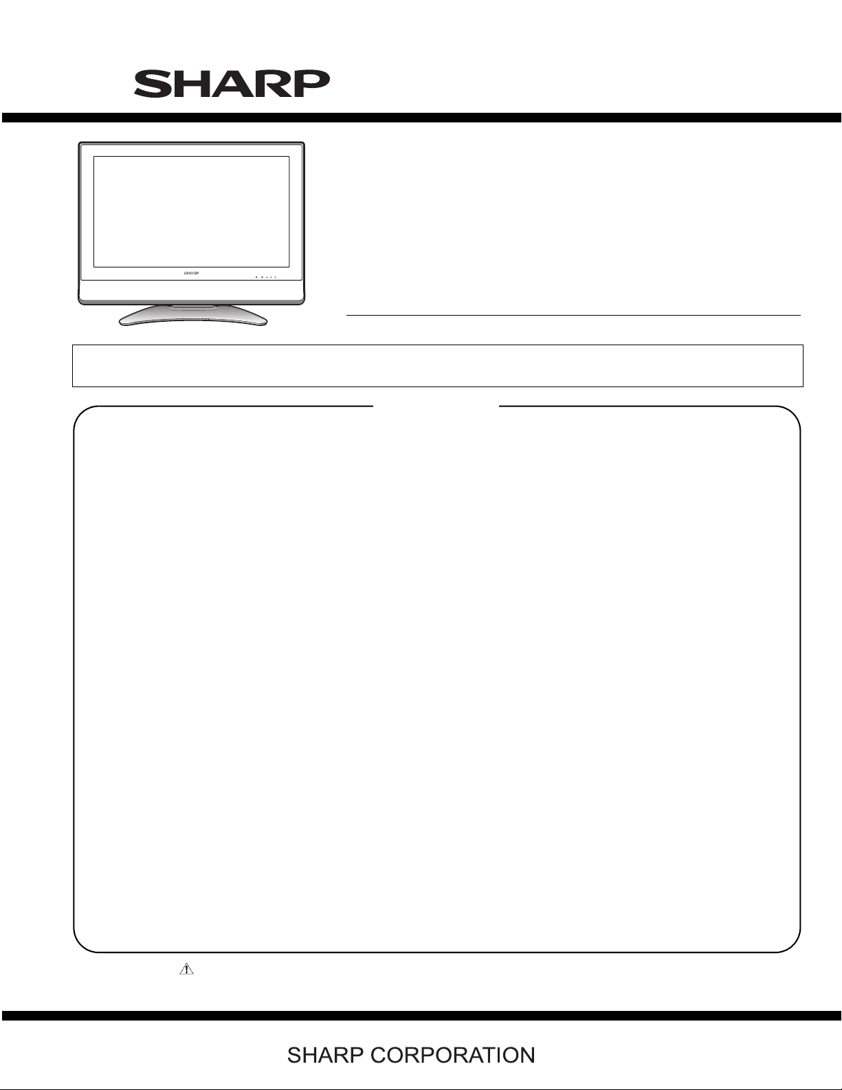
TopPage
LC-26SA1E/RU, LC32SA1E/RU
SERVICE MANUAL
No. S66U9LC26SA1E
LCD COLOUR TELEVISION
LC-26SA1E/RU
MODELS
In the interests of user-safety (Required by safety regulations in some countries) the set should be restored to its original condition and only parts identical to those specified should be used.
LC-32SA1E/RU
CONTENTS
SAFETY PRECAUTION
IMPORTANT SERVICE SAFETY PRECAUTION
Precautions for using lead-free solder ...............ii
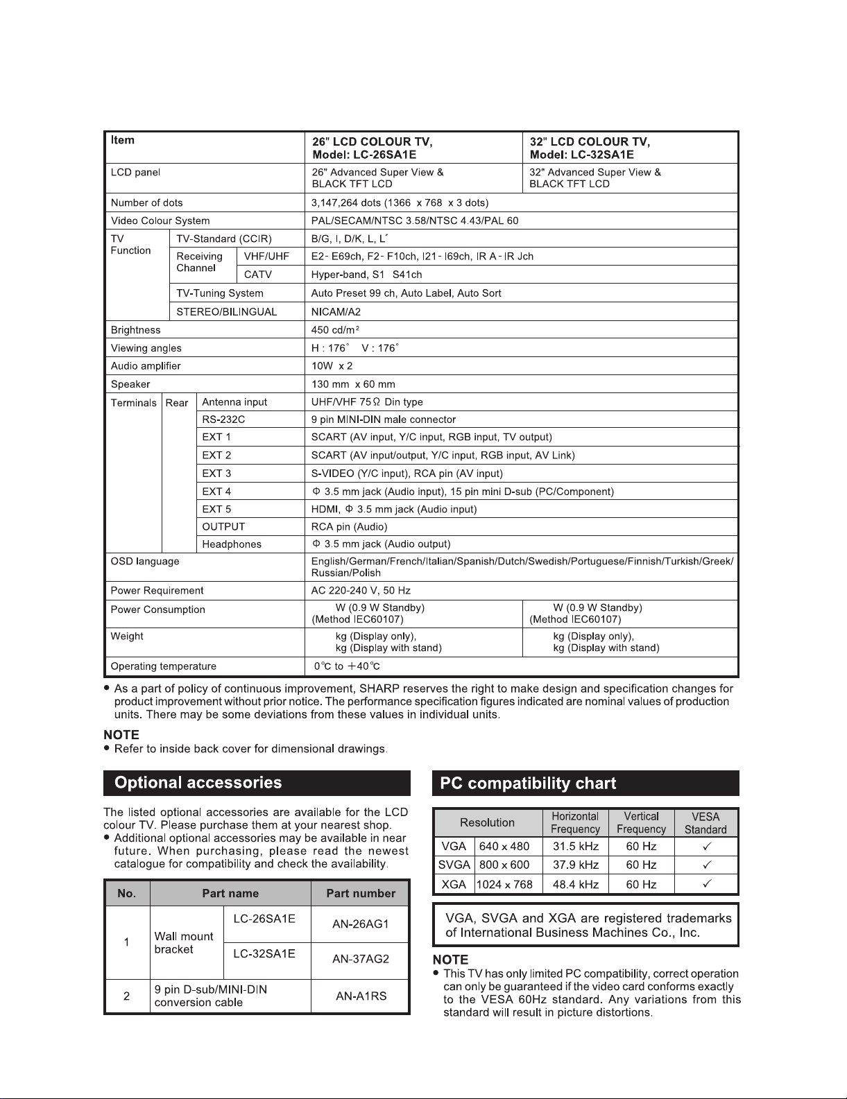
CHAPTER 1. SPECIFICATIONS
[1] SPECIFICATIONS .........................................1-1
CHAPTER 2. OPERATION MANUAL
[1] OPERATION MANUAL.................................. 2-1
CHAPTER 3. DIMENSIONS
[1] DIMENSIONS ................................................ 3-1
CHAPTER 4. REMOVING OF MAJOR PARTS
[1] REMOVING OF MAJOR PARTS
LC-26SA1E/RU..............................................4-1
[2] REMOVING OF MAJOR PARTS
LC-32SA1E/RU..............................................4-5
CHAPTER 5. ADJUSTMENT PROCEDURE
[1] After replacement of any PWB and/or IC for
repair, note the following................................5-1
[2] SOFTWARE UPDATING................................ 5-1
[3] Entering and exiting the adjustment pro-
cess mode.................................................... 5-11
Remote controller key operation and descrip-
[4]
tion of display in adjustment process mode
[5] Adjustment process mode menu..................5-12
[6] Special features............................................5-13
[7] Video signal adjustment procedure..............5-14
[8] White Balance Adjustment...........................5-16
.............i
....... 5-11
[9] QS Temperature NVM Data Con?rmation......5-17
[10] Initialization to factory settings.....................5-17
[11] Lamp error detection ...................................5-18
[12] Public Mode (Hotel Mode)...........................5-18
CHAPTER 6. TROUBLESHOOTING T ABLE
[1] TROBLESHOOTING TABLE.........................6-1
CHAPTER 7. MAJOR IC INFORMATIONS
[1] MAJOR IC INFORMATIONS.........................7-1
CHAPTER 8. OVERALL WIRING DIAGRAM/BLOCK
DIAGRAM
[1] OVERALL WIRING DIAGRAM......................8-1
[2] BLOCK DIAGRAM.........................................8-3
[3] POWER BLOCK DIAGRAM..........................8-5
CHAPTER 9. PRINTED WIRING BOARD
OPERATION UNIT PRINTED WIRING BOARD
[1]
R/C, LED UNIT PRINTED WIRING BOARD
[2]
[3] MAIN UNIT PRINTED WIRING BOARD........9-3
[4] AV UNIT PRINTED WIRING BOARD..........9-11
[5] POWER UNIT PRINTED WIRING BOARD......9-17
[6] TUNER UNIT PRINTED WIRING BOARD......9-21
CHAPTER 10. SCHEMATIC DIAGRAM
DESCRIPTION OF SCHEMATIC DIAGRAM
[1]
[2] SCHEMATIC DIAGRAM..............................10-2
Parts Guide
........9-1
........9-2
......10-1
Parts marked with " " are important for maintaining the safety of the set. Be sure to replace these parts with specified ones for maintaining the
safety and performance of the set.
This document has been published to be used for
after sales service only.
The contents are subject to change without notice.
Page 2
LC-26SA1E/RU, LC-32SA1E/RU
LC-26SA1E
SAFETY PRECAUTION
Service Manual
IMPORTANT SERVICE SAFETY PRECAUTION
Service work should be performed only by qualified service technicians who are thoroughly familiar with all safety checks and the
servicing guidelines which follow:
WARNING
1. For continued safety, no modification of any circuit should be
attempted.
2. Disconnect AC power before servicing.
CAUTION:
FOR CONTINUED PROTECTION AGAINST A
RISK OF FIRE REPLACE ONLY WITH SAME
TYPE FUSE.
• Use an AC voltmeter having with 5000 ohm per volt, or higher, sensitivity or measure the AC voltage drop across the resistor.
• Connect the resistor connection to all exposed metal parts having a
return to the chassis (antenna, metal cabinet, screw heads, knobs
and control shafts, escutcheon, etc.) and measure the AC voltage
drop across the resistor.
All checks must be repeated with the AC cord plug connection
reversed. (If necessary, a nonpolarized adaptor plug must be used
only for the purpose of completing these checks.)
Any reading of 1.05 V peak (this corresponds to 0.7 mA peak AC.)
or more is excessive and indicates a potential shock hazard which
must be corrected before returning the monitor to the owner.
F701 (4A/250V)
BEFORE RETURNING THE RECEIVER
(Fire & Shock Hazard)
Before returning the receiver to the user, perform the following
safety checks:
3. Inspect all lead dress to make certain that leads are not pinched,
and check that hardware is not lodged between the chassis and
other metal parts in the receiver.
4. Inspect all protective devices such as non-metallic control knobs,
insulation materials, cabinet backs, adjustment and compartment
covers or shields, isolation resistor-capacitor networks, mechanical
insulators, etc.
5. To be sure that no shock hazard exists, check for leakage current in
the following manner.
• Plug the AC cord directly into a 220~240 volt AC outlet.
• Using two clip leads, connect a 1.5k ohm, 10 watt resistor paralleled by a 0.15µF capacitor in series with all exposed metal cabinet
parts and a known earth ground, such as electrical conduit or electrical ground connected to an earth ground.
///////////////////////////////////////////////////////////////////////////////////////////////////////////////////////////////////////////////////////////////////////////////////////////////////////////////////////////////////////////
TO EXPOSED
METAL PARTS
SAFETY NOTICE
Many electrical and mechanical parts in LCD color television have
special safety-related characteristics.
These characteristics are often not evident from visual inspection, nor
can protection afforded by them be necessarily increased by using
replacement components rated for higher voltage, wattage, etc.
Replacement parts which have these special safety characteristics are
identified in this manual; electrical components having such features
are identified by “ ” and shaded areas in the Replacement Parts
List and Schematic Diagrams.
///////////////////////////////////////////////////////////////////////////////////////////////////////////////////////////////////////////////////////////////////////////////////////////////////////////////////////////////////////////
For continued protection, replacement parts must be identical to those
used in the original circuit.
The use of a substitute replacement parts which do not have the same
safety characteristics as the factory recommended replacement parts
shown in this service manual, may create shock, fire or other hazards.
DVM
AC SCALE
1.5k ohm
10W
0.15µF
TEST PROBE
CONNECT TO
KNOWN EARTH
GROUND
i
Page 3
LC-26SA1E/RU, LC-32SA1E/RU
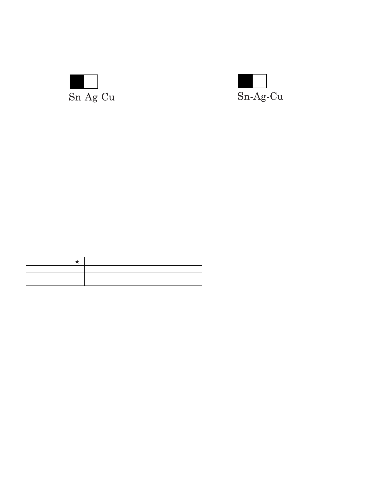
Precautions for using lead-free solder
Employing lead-free solder
• “PWBs” of this model employs lead-free solder. The LF symbol indicates lead-free solder, and is attached on the PWBs and service manuals. The
alphabetical character following LF shows the type of lead-free solder.
Example:
L Fa
Indicates lead-free solder of tin, silver and copper.
Indicates lead-free solder of tin, silver and copper.
L F a/a
Using lead-free wire solder
• When fixing the PWB soldered with the lead-free solder, apply lead-free wire solder. Repairing with conventional lead wire solder may cause damage or accident due to cracks.
As the melting point of lead-free solder (Sn-Ag-Cu) is higher than the lead wire solder by 40 °C, we recommend you to use a dedicated soldering
bit, if you are not familiar with how to obtain lead-free wire solder or soldering bit, contact our service station or service branch in your area.
Soldering
• As the melting point of lead-free solder (Sn-Ag-Cu) is about 220 °C which is higher than the conventional lead solder by 40 °C, and as it has poor
solder wettability, you may be apt to keep the soldering bit in contact with the PWB for extended period of time. However, Since the land may be
peeled off or the maximum heat-resistance temperature of parts may be exceeded, remove the bit from the PWB as soon as you confirm the
steady soldering condition.
Lead-free solder contains more tin, and the end of the soldering bit may be easily corroded. Make sure to turn on and off the power of the bit as
required.
If a different type of solder stays on the tip of the soldering bit, it is alloyed with lead-free solder. Clean the bit after every use of it.
When the tip of the soldering bit is blackened during use, file it with steel wool or fine sandpaper.
• Be careful when replacing parts with polarity indication on the PWB silk.
Lead-free wire solder for servicing
Part No. Description Code
ZHNDAi123250E J φ0.3mm 250g (1roll) BL
ZHNDAi126500E J φ0.6mm 500g (1roll) BK
ZHNDAi12801KE J φ1.0mm 1kg (1roll) BM
ii
Page 4
LC-26SA1E/RU, LC-32SA1E/RU
LC-26SA1E
CHAPTER 1. SPECIFICATIONS
[1] SPECIFICATIONS
Service Manual
/RU /RU
-
102
13.0
15.2
125
17.9
20.1
1 – 1
Page 5
LC-26SA1E
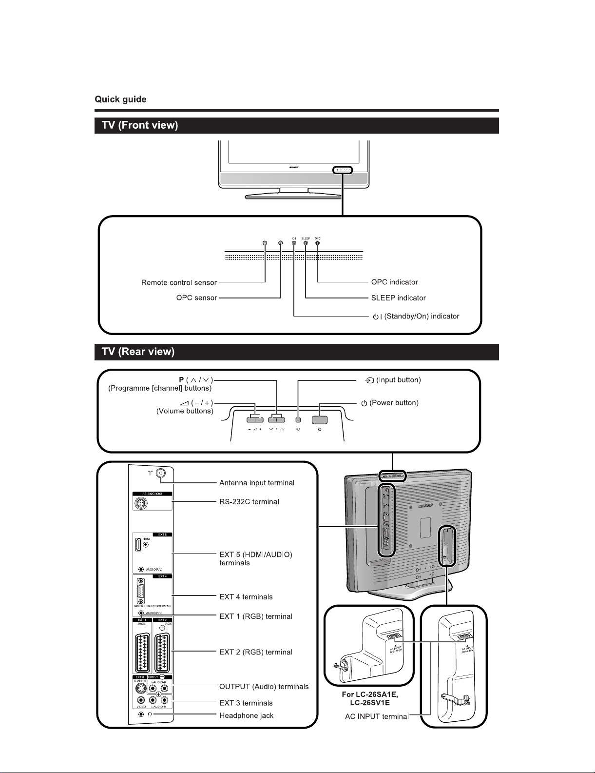
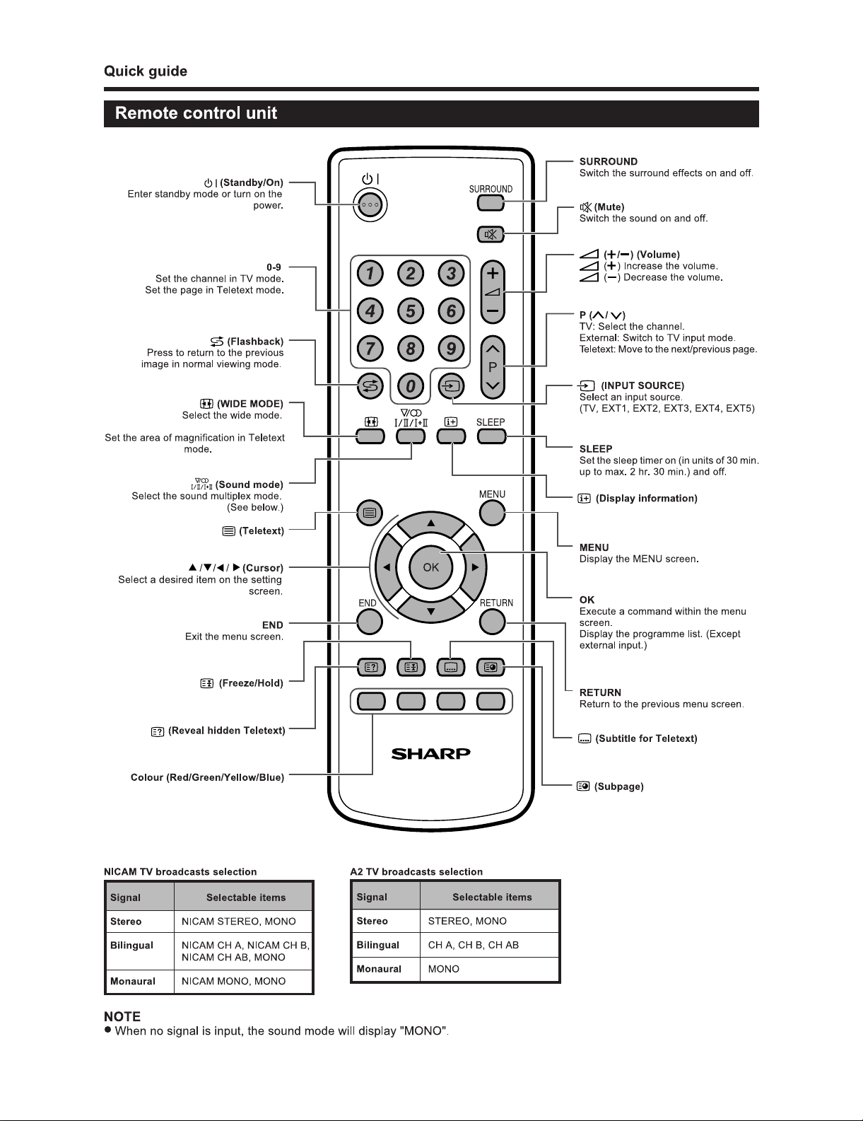
CHAPTER 2. OPERATION MANUAL
[1] OPERATION MANUAL
LC-26SA1E/RU, LC-32SA1E/RU
Service Manual
2 – 1
Page 6
LC-26SA1E/RU, LC-32SA1E/RU
2 – 2
Page 7
LC-26SA1E
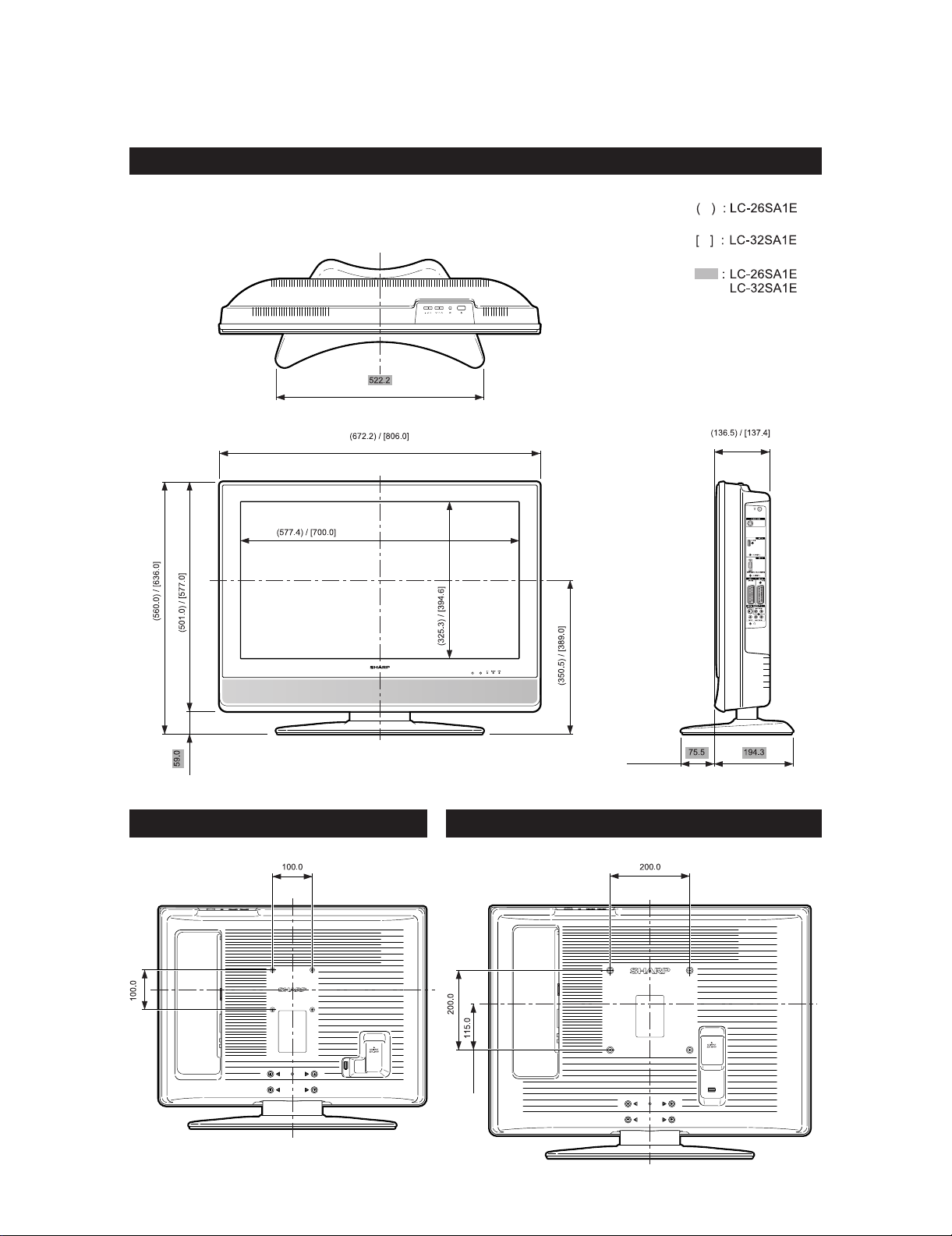
CHAPTER 3. DIMENSIONS
[1] DIMENSIONS
LC-26SA1E/RU / LC-32SA1E/RU
LC-26SA1E/RU, LC-32SA1E/RU
Service Manual
/RU
/RU
/RU
/RU
LC-26SA1E/RU
LC-32SA1E/RU
3 – 1
Page 8
LC-26SA1E/RU, LC-32SA1E/RU
LC-26SA1E
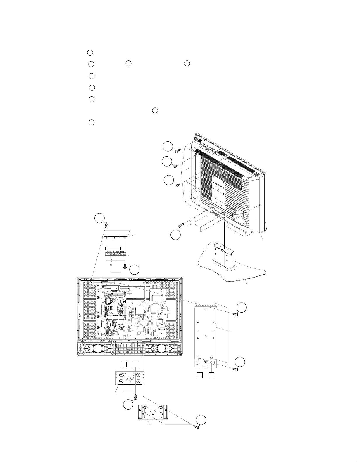
CHAPTER 4. REMOVING OF MAJOR PARTS
Service Manual
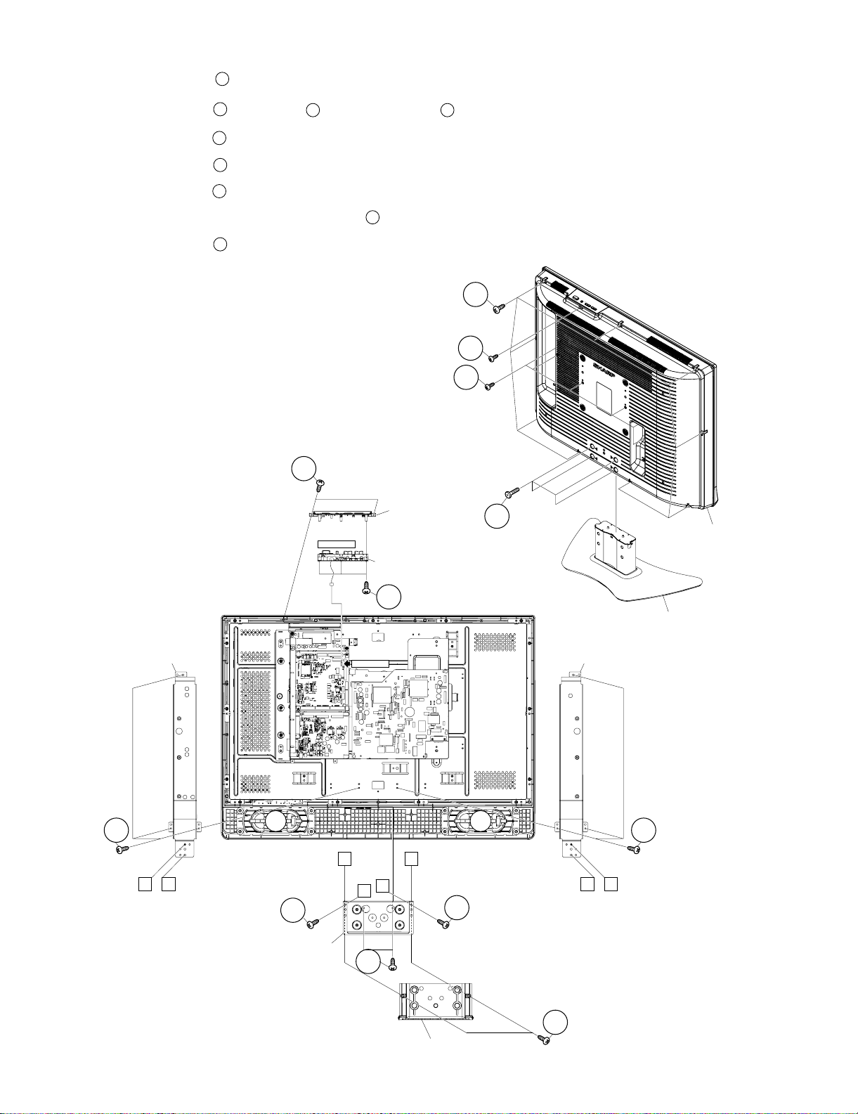
[1] REMOVING OF MAJOR PARTS LC-26SA1E/RU
1. Remove the 4 lock screws . Detach the Stand.
2. Remove the 3 lock screws . 1 lock screw and the 9 lock screws . Detach the Rear Cabinet.
3. Remove the 2 lock screws and detach the Bottom Cover.
4. Remove the 2 lock screws and detach the Stand Angle.
5. Remove the 5 lock screws and detach the Center Angle.
6. Disconnect the KM connector. Remove the 2 lock screws and detach the Top Cover Ass’y.
7. Remove the 3 lock screws and detach the KEY Unit.
1
2
5
6
7
9
3 4
8
4
3
2
8
KM(P169)
Stand Angle
Key Unit
KM(P2302)
A B
6
Top Cover Ass'y
9
1
Rear Cabinet
Stand
7
Center Angle
7
A B
Bottom Cover
5
4 – 1
Page 9
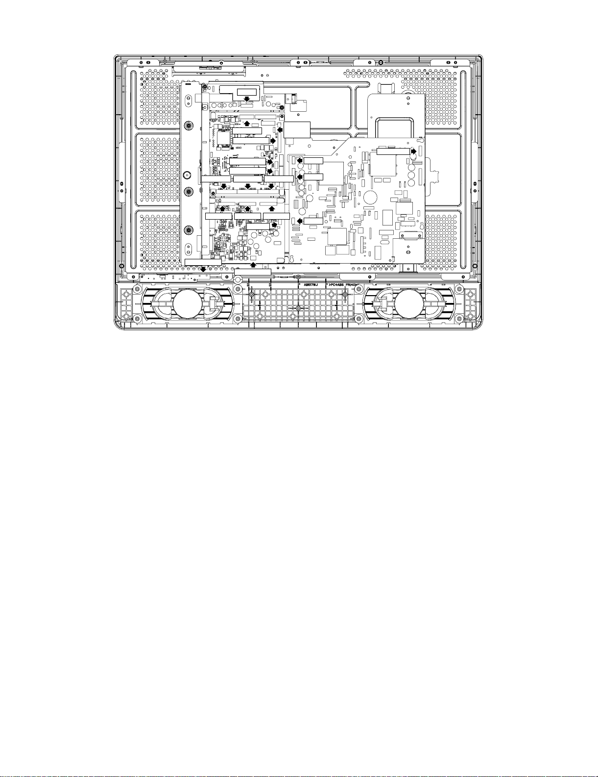
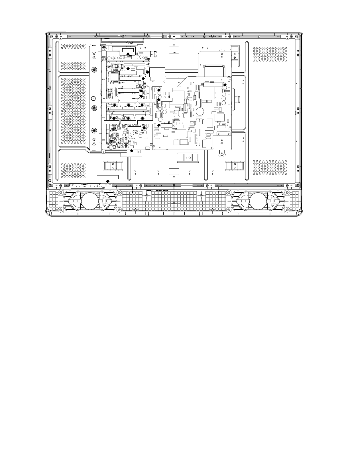
8. Remove all the connectors from PWBs.
LC-26SA1E/RU, LC-32SA1E/RU
P201
RA(P101)
SC2705
LV(P2305)
SH(P2301)
RA(P2303)
SC2703SC2702 SC2704
P1102P1101 P1201
SC301
SP(P301)
KM
P2302
LA(P704)
P702
P701
P703
4 – 2
Page 10
LC-26SA1E/RU, LC-32SA1E/RU
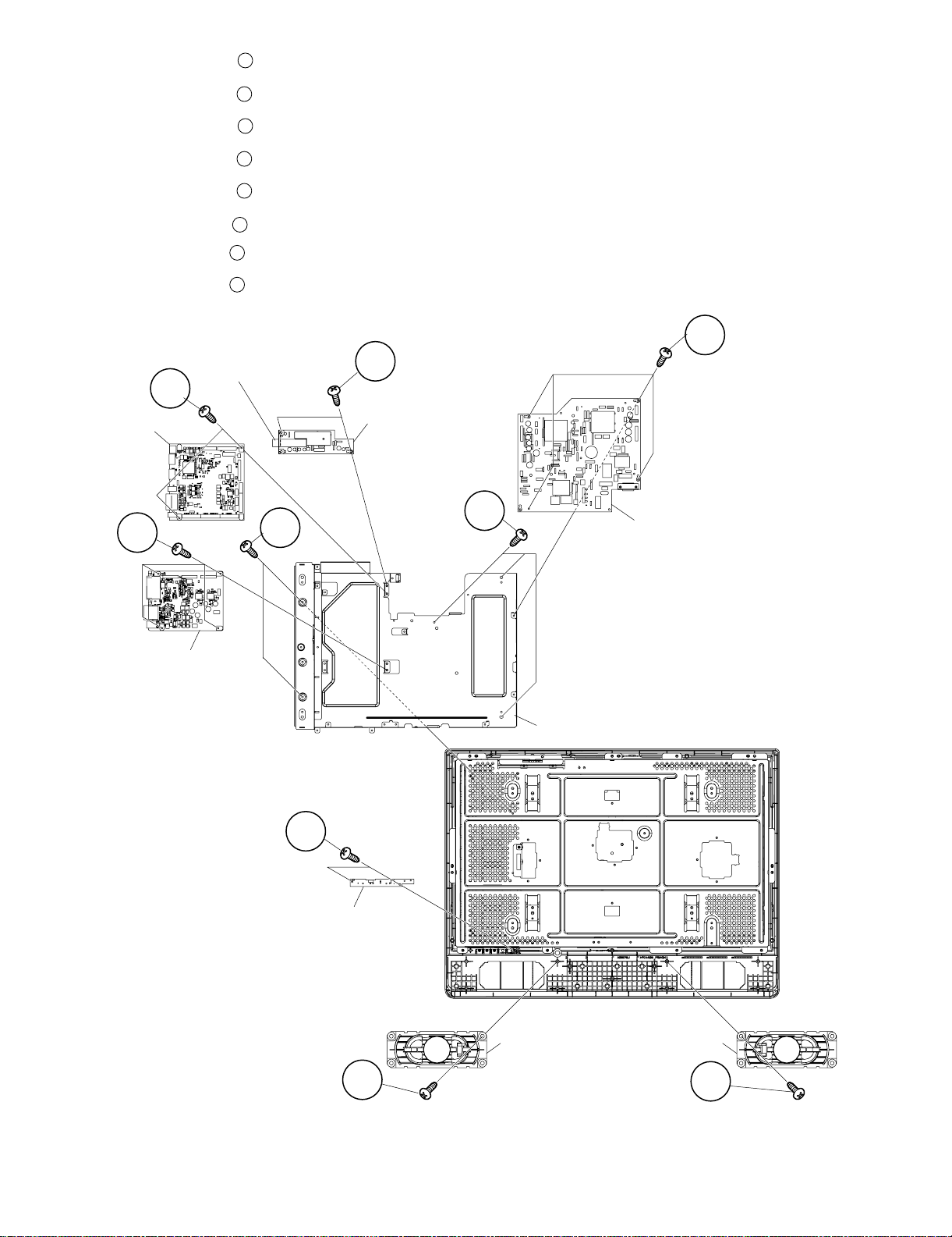
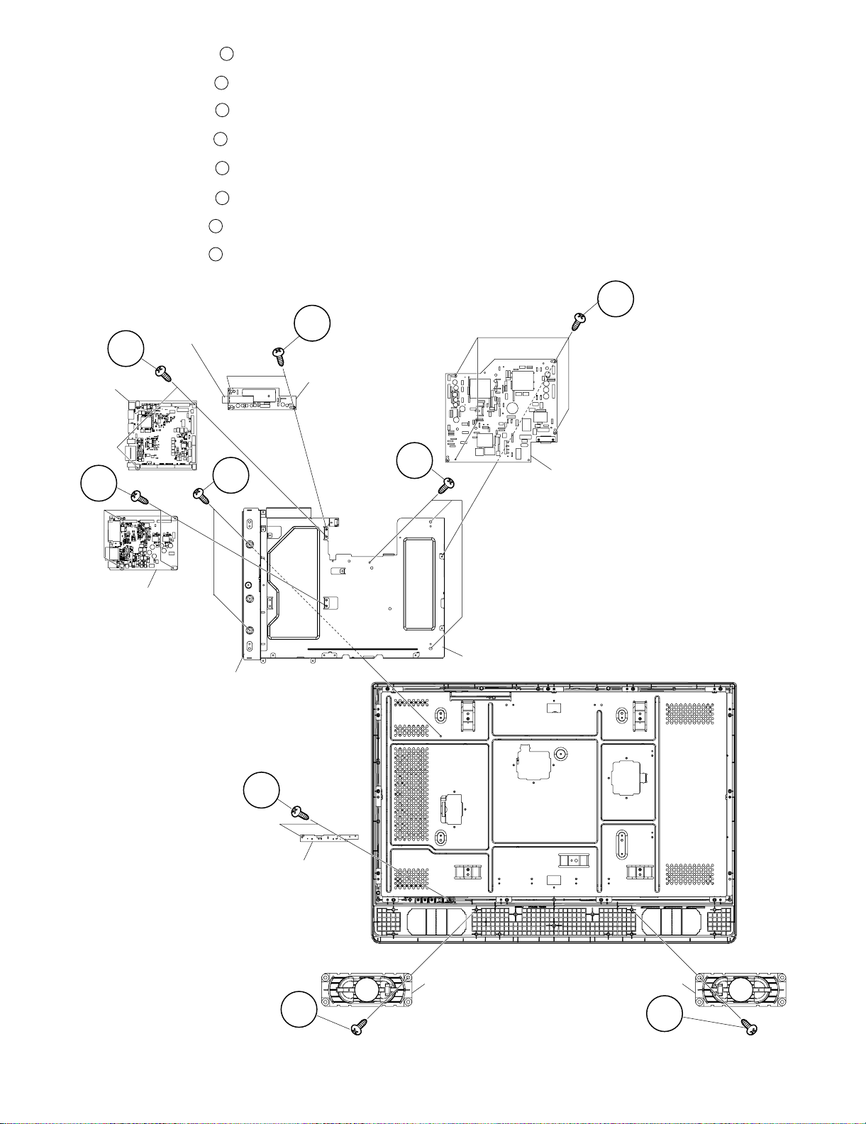
9. Remove the 4 lock screws and detach the Power Unit.
10
10.Remove the 2 lock screws and detach the Tuner Unit and Tuner Earth Plate.
11.Remove the 2 lock screws and detach the Main Unit.
12.Remove the 4 lock screws and detach the AV Unit.
13.Remove the 5 lock screws detach the Chassis Tray.
14.Remove the 2 lock screws and detach the R/C, LED Unit.
15.Remove the 1 lock screw and detach the Speaker R.
16.Remove the 1 lock screw and detach the Speaker L.
11
12
13
14
15
16
17
Tuner Earth Plate
11
12
Main Unit
Tuner Unit
14
13
14
10
Power Unit
AV Unit
15
R/C,LED Unit
16
Chassis Tray
Speaker R
Speaker L
17
4 – 3
Page 11
LC-26SA1E/RU, LC-32SA1E/RU
17.Remove the 8 lock screws and the 6 lock screws , detach the LCD Angle.
18.Remove the LCD Panel Unit from Front Cabinet.
18
19
18
19
18
LCD Angle
LCD Panel Unit Front Cabinet
18
19
18
4 – 4
Page 12
LC-26SA1E/RU, LC-32SA1E/RU
[2] REMOVING OF MAJOR PARTS LC-32SA1E/RU
1. Remove the 4 lock screws . Detach the Stand.
2. Remove the 6 lock screws . 1 lock screw and the 9 lock screws . Detach the Rear Cabinet.
3. Remove the 2 lock screws and detach the Bottom Cover.
4. Remove the 4 lock screws and detach the Stand Angle.
5. Remove the 6 lock screws and detach the Center Angle L and the Center Angle R.
6. Disconnect the KM connector. Remove the 2 lock screws and detach the Top Cover Ass’y.
7. Remove the 3 lock screws and detach the KEY Unit.
1
2
5
6
7
9
3 4
8
4
3
2
8
Center Angle R
7
Top Cover Ass'y
KM(P169)
Key Unit
1
Rear Cabinet
9
Stand
KM(P2302)
Center Angle L
7
D
A
D
A
6
C
B
B
C
6
Stand Angle
6
5
Bottom Cover
4 – 5
Page 13
8. Remove all the connectors from PWBs.
LC-26SA1E/RU, LC-32SA1E/RU
P201
RA(P101)
SC2705
LV(P2305)
SH(P2301)
RA(P2303)
SC2703SC2702 SC2704
P1102P1101 P1201
SC301
SP(P301)
KM
P2302
LA(P704)
P702
P701
P703
4 – 6
Page 14
LC-26SA1E/RU, LC-32SA1E/RU
9. Remove the 4 lock screws and detach the Power Unit.
10
10.Remove the 2 lock screws and detach the Tuner Unit and Tuner Earth Plate.
11.Remove the 2 lock screws and detach the Main Unit.
12.Remove the 4 lock screws and detach the AV Unit.
13.Remove the 5 lock screws detach the Terminal Angle and the Chassis Tray.
14.Remove the 2 lock screws and detach the R/C,LED Unit.
15.Remove the 1 lock screw and detach the Sperker R.
16.Remove the 1 lock screw and detach the Sperker L.
Tuner Earth Plate
11
12
13
14
15
16
17
11
12
Main Unit
Tuner Unit
14
13
14
10
Power Unit
AV Unit
Terminal Angle
15
R/C,LED Unit
Chassis Tray
Speaker R
Speaker L
16
17
4 – 7
Page 15
17.Remove the 8 lock screws and the 5 lock screws , Detach the LCD Angle.
18.Remove the LCD Panel from Front Cabinet.
18
19
LC-26SA1E/RU, LC-32SA1E/RU
19
18
18
LCD Angle
LCD Panel Unit Front Cabinet
18
19
18
4 – 8
Page 16
LC-26SA1E/RU, LC-32SA1E/RU
LC-26SA1E
CHAPTER 5. ADJUSTMENT PROCEDURE
The adjustment values are set to their optimum at the factory before shipping.
If by any chance a value should become improper or a readjustment is required due to part replacement, make an adjustment according to the fol-
lowing procedure.
Service Manual
[1] After replacement of any PWB and/or IC for repair, note the following.
When replacing the following units, be sure to prepare the new units loaded with updated software.
MAIN-UNIT : DUNTKD890FM12 (LC-26SA1E/K/F/I/RU)
DUNTKD890FM13 (LC-32SA1E/K/F/I/RU)
• Note that an IC into which ROM data is written is available for MAIN-UNIT servicing (see below)
IC1901 VHi24LC2BiNEES EDID(HDMI)
IC2303 RH-iXB731WJZZS EDID(PC)
[2] SOFTWARE UPDATING
There are 3 methods to update software in the VCTp: I2C method, RS-232C HyperTerminal and RS-232C Tera Term method.
• RS-232C method is allowed when the TV is working properly and the action should be only software upgrade.
• I2C method is required when the VCTp fiash is empty or corrupted (it means, any software inside IC running).
1. RS-232C Method Description (HyperTerminal).
The hardware tools requirement are:
1. A Modem-null (Cross type) DB9 female to DB9 female cable.
2. An adaptor DB9 male to mini-Din 9 pin male cable (Sharp Code: QCNWGA015WJPZ)
3. Make the connections as indicated in the figure:
Computer TV set
Before using RS-232C updating method is necessary to configure a Terminal PC software. HyperTerminal has been selected as a Terminal software because it’s include in all Windows versions as an accessory, and you can find it inside “Accessories\Communications” folder. For this reason, please follow carefully the next steps:
1) First time HyperTerminal is used, it’s necessary to configure some settings. Follows next action to configure two connection: low speed
(9600bps) and high speed (115200bps).
2) Create a New Connection file with name “P55_9600bps”.
3) Select a free COM port and select the Port Settings properties as follows:
5 – 1
Page 17
4) Click on “File\Properties” menu for selecting the General and ASCII properties as follows:
5) Select “New Connection” in the File Menu.
6) Answer “Yes” to close current connection and”Yes” to save session “P55_9600bps”.
7) Create a new connection with the name “P55_115200bps”.
8) Select a the same COM port used in item 2 and select the Port Settings properties as follows:
LC-26SA1E/RU, LC-32SA1E/RU
9) Select the same General and ASCII properties as item 3.
10)Close HyperTerminal session, answering “Yes” to close current connection and “Yes” to save session “P55_115200bps”.
To start updating session, click over “P55_9600bps” icon that you can find in the “START\All programs\Accessories\ Communications\HyperTermi-
nal\HyperTerminal” folder and follow next procedure:
5 – 2
Page 18

LC-26SA1E/RU, LC-32SA1E/RU
1) Check the connection between TV set and PC, sending a wrong command, as for example: “aaa”. TV set returns an “ERR” label as an syntaxis
ERROR (Not correct order or sequence).
2) Send the command “DWMD” to enter TV set in Download Mode. The TV set answer sending same symbol continuosly. If this symbol character
doesn’t appear, please don’t worry and pass to next step.
3) Close this connection and open “P55_115200bps” connection clicking over the “P55_115200bps” that you can find in “START\All pro-
grams\Accessories\ Communications\HyperTerminal\HyperTerminal” folder.
4) Using “Transfer\Send file...” menu, select desired file (.bin format) and the transmission protocol (Xmodem) as show below.
5) After press “Send” button the updating process starts as follows:
6) When flash update process finishes, the”Flash Programming Complete” label appears in the screen.
VERY IMPORTANT NOTE:
During the updating time, please don’t use the PC for other purpouses, in order to abolish commu nication problems between TV set an d
PC. If TV set was not updated properly, the TV won’t have the software to startup again, and you must follow the “I2C method” to update
another time the TV set.
5 – 3
Page 19

2. RS-232C Method Description (Tera Term)
The hardware tools requirement are:
1. A Modem-null (Cross type) DB9 female to DB9 female cable.
2. An adaptor DB9 male to mini-Din 9 pin male cable (Sharp Code: QCNWGA015WJPZ)
3. Make the connections as indicated in the figure:
LC-26SA1E/RU, LC-32SA1E/RU
Software requirements :
To upgrade VCTp software from RS-232C external connector is necessary to use a Tera Ter m (Pro) free software.
The URL of Tera Term home page is:
http://hp.vector.co.jp/authors/VA002416/teraterm.html
(The address may be changed in future)
Tera Term (Pro) supported operating systems:
MS-Windows 95 or upper
MS-Windows NT 3.5 and 4.0 or upper
Note.- For Windows 3.1 use Tera Term version 1.X.
Copy all the distribution files to an empty floppy disk or temporary directory (for example C:\ TEMP ).
Run SETUP.EXE and follow the instruction given by it.
After the installation, the distribution ?les are no longer needed, you can delete them or may keep them in the floppy disk.
How to use Tera Term Pro :
When the Tera Term (Pro) program is used, it’s necessary to shape some settings. Follows next action to configure the connection:
5 – 4
Page 20
LC-26SA1E/RU, LC-32SA1E/RU
1) Select: Serial→COM X→ O.K.
2) Select: Terminal
3) Choose the same options as the above picture.
5 – 5
Page 21

4) Select: Setup → Serial port → O.K. Appear the follow screen:
5) Select follows settings:
Serial port to use: COM x
Baud rate: 9600
Data: 8 bits
Parity: none
Stop: 1 bit
Flow control: none
Enter O.K.
LC-26SA1E/RU, LC-32SA1E/RU
6) Check the connection between TV set and PC, sending a wrong command, as for example: “aaa”. TV set returns an “err” label as an syntaxes
ERROR (Not correct order or sequence).
Send a “DWMD” (capital letters) command to enter TV set in Download Mode.
Change a baud rate to 115200.
Select: Setup → Baud rate → 115200 → O.K.
5 – 6
Page 22

LC-26SA1E/RU, LC-32SA1E/RU
7) Select: File → Transfer → XMODEM → Sent
8) Choose the file for upgrade and click “Open”.
9) After select “Open” the upgrade process starts as follows:
5 – 7
Page 23
LC-26SA1E/RU, LC-32SA1E/RU
10)When flash update process finishes, the “Flash programming complete” label appear in the screen , the device automatically go to switch off, and
in a few seconds go to switch on again.
VERY IMPORTANT NOTE:
During the updating time, please don’t use the PC for other purposes, in order to abolish communication problems between TV set and PC.
If TV set was not updated properly, the TV wonÅft have the software to startup again, and you must follow the “I2C method”
another time the TV set.
3. I2C Method Description
The hardware tools requirement are:
1. A Parallel port I2C interface with 20 pin to 3 pin cable (Sharp Code: CKIT-0004WJV0).
2. Make the connections as indicated below:
i) Connect Parallel port I2C interface to LPT port of the computer.
ii) Connect the 20 to 3 pin cable from the I2C interface to the P2306 socket in the main board (XD603).
to update
To P2306
To PC
QCNWGA100WJZZ
QPWBX0004WJZZ
I2C Interface (CKIT-0004WJV0)
Before using I2C method is necessary to install Visual I2C software following next procedure.
1. Install Visual I2C release V3.2.3b from file (“Setup_Visual_I2C_v3-2-3b8h.exe”).
• It’s strongly recommended to accept the suggested default folder (“C:\Program Files\Micronas\Visual I2C”).
2. Install Visual I2C VCTp extension from file (“Setup_VI2C_for_VCT6wxyP_v0111.exe”).
• It’s interesting to change default folder to same as Visual I2C (“C:\Program Files\Micronas\Visual I2C”).
• During this installation process is possible to install also a complementary software to manage NVM memories .
This installation is not needed, for this reason uncheck the option when the setup program ask to you. In case of installation it’s interesting to change
default folder to same as Visual I2C (“C:\Program Files\Micronas\Visual I2C”).
3. Install Parallel driver depending of your Windows version from existing files inside the Visual I2C installation folder “C:\Program Files\Micro
nas\Visual I2C\Port_Driver”, following next criteria:.
1) Windows 98/Me (“Setup_LptDrv_v0104_9x.exe”).
2) Windows NT (“Setup_LptDrv_v0104_NT_2000.exe”).
5 – 8
Page 24
LC-26SA1E/RU, LC-32SA1E/RU
3) Windows Xp/2000 (“Setup_LptDrv_v020201_XP_2000.exe”).
After installing Visual I2C, the new generated file structure should look like this:
4. Check installation LPT driver using “C:\Program Files\Micronas\LptDrv\LptDrvTest.exe”. After run this software, if LPT driver is installed properly
must appear this screen:
3.
• If the result is not OK, check inside PC bios: Parallel Port Mode=EPP
To run VCTp software update program, please click over “VCTP” icon from “START\All programs\Micronas\Visual I2C\IC\VCTP” and after Visual I2C
finish their starting process click on “TVT” module. As additional method, it’s possible to create a direct access to “C:\Program Files\Micronas\Visual
I2C\ic\vct6wxyP\vctq_tvt.vi2c” and launch it from Windows Desktop.
1
5
2
4
2
4
3
67
67
5 – 9
Page 25
LC-26SA1E/RU, LC-32SA1E/RU
To start updating process follow next instructions:
1. Set Autoread in ON option.
2. Click on “GO” button.
3. Wait until “40” appears in Bootloader Version field.
4. Close DOS pop up windows pressing any key (“Press any key to continue...”.).
5. Click on the “Erase flash” button and wait for a seconds and set the AutoRead to OFF.
6. Check in the desired software version is selected in the “Load BinaFlash” option. If it’s not the correct one, please double click on the file name and
select it. The first time this software is use it’s necessary to confirm write Addressing margin as from 0x0 to 0x7ffff.
7. Click on the “Load Bin → Flash” to start updating process.
8. When the updating process finishes, the “Progress” pop up window automatically closes. If appears some problem during the updating process a
error label appears in the filename information line.
If the TV has problem to enters in the”Bootloader mode”, it’s possible to force it by hardware method. This alternative method is described
below:
1. Switch off TV set or hold VCTp RESET line to GND.
2. Pull down SCL line (pin 1) to GND (pin 3) in P2306 connector.
3. Switch on TV set or release VCTp RESET line.
4. Release SCL pull down after minimum of 2 seconds.
5. Check if VCTp is in bootloader mode with Autoread setting in ON.
6. Wait until “40” appears in Bootloader Version field.
7. Follow instruction from item 5 on software method.
Sometimes, depending on the PC hardware, the progress bar runs very fast (Normal time: 1 minute) or some error message appears in the filename
information line. This means it’s necessary to modify some parameter of LPT port, for this reason select “LPT Preferences” on the “File\Preferences...” menu and increase Delay from “0” to “1” or “2” (normally, these values are the best choice).
5 – 10
Page 26
LC-26SA1E/RU, LC-32SA1E/RU
[3] Entering and exiting the adjustment process mode
1) Unplug the AC power cord of running TV set to force off the power.
2) While holding down the “VOL(-)” and ”INPUT” keys on the set at once, plug in the AC power cord to turn on the power. The letter appears on
the screen.
3) Next, hold down the ”VOL(-)” and ”P( )” keys on the set at once.
Multiple lines of orange characters appearing on the screen indicate that the set is now in the adjustment Process mode. If you fail to enter the
adjustment process mode (the display is the same as normal startup), retry the procedure.
4) To exit the adjustment process mode after the adjustment is done, unplug the AC power cord to force off the power. (When the power is turned off
with the remote controller, once unplug the AC power cord and plug it in again. In this case, wait 10 seconds or so before plugging.)
5) To remove “K” mode holding down the “VOL (-)” and “INPUT” kyes on the set at once (“K” disappears).
K
Caution : Use due care in handling the information described here lest the users should know how to enter the adjustment process mode. If the
settings are tampered with in this mode, unrecoverable system damage may result.
[4] Remote controller key operation and description of display in adjustment process mode.
1. key operation
Remote controller key Main unit key Function
P ( / ) P ( / )
VOL (+ / –) VOL (+ / –) Changing a selected item setting (+1/–1)
Cursor (UP/DOWN) —————— Turning a page (PREVIOUS/NEXT)
Cursor (LEFT/RIGHT) —————— Changing a selected line setting (+10/–10)
INPUT SOURCE
INPUT button Input source switching (toggle switching)
on remote controller
OK —————— Executing a function
* Input mode is switched automatically when relevant adjustment is started so far as the necessary input signal is available.
2. Description of display
(1) Current page/Total pages (3) Currently selected input
(2) Current page title
1/11
Main Version
Dev Version
Dev Loader Version
Pic Version
TEMP SENSOR
NORMAL STANDBY CAUSE
ERROR STANDBY CAUSE
[INFO] TV AUTO 32 EURO
1.XX (XX/XX/XXX)
XX
XX
XX
XX
XX
XX
Moving an item (line) by one (UP/DOWN)
(TV→EXT1→EXT2→EXT3→EXT4→EXT5)
(4) Current colour TV system
Inch Setting (32 just as example, it may be: --/26/32)
(5)
Destination (EURO just as example.
See Factory Init,it may be EURO, UK,
ITALY, FRANCE or RUSSIA)
Adjustment process
menu header
(7) Parameters
5 – 11
Page 27
LC-26SA1E/RU, LC-32SA1E/RU
[5] Adjustment process mode menu
The character string in brackets [ ] will appear as a page title in the adjustment process menu header.
Page Line Item Description Remarks (adjustment detail, etc.)
1/11 [INFO]
1 Main Version LEW05 01.03(2006/07/15x)5 Main microprocessor version
2 Dev Version xxxxxx
3 Dev Loader Version xxxxxx
4 Pic Version xxxxxx Pic MICON version
5 TEMP SENSOR xxxxxx Temp inside the cabinet
6 NORMAL STANDBY CAUSE 1 RC_STANDBY Last status which cause standby
7 ERROR STANDBY CAUSE [1] 0 00H 00M Error standby cause Total operating time before error
[2] 0 00H 00M
[3] 0 00H 00M
[4] 0 00H 00M
[5] 0 00H 00M
2/11 [INIT]
1 Factory Init [EURO]ENTER Initialization to factory settings execution
2 Inch Setting 26/32/37/42 Inch present setting
3 Public Mode OFF/ON HOTEL MODE flag setting
4 Center Acutime xxH xxM Main operating hours
5 RESET OFF/ON Main operating hours reset
6 Backlight Acutime xxH xxM Backlight operating hours
7 RESET OFF/ON Backlight operating hours reset
8 Picture Read Pos X 0-xxx x-axis setting of picture data
9 Picture Read Pos Y 0-xxx y-axis setting of picture data
10 Picture Read ON/OFF Start/stop of picture data
3/11 [PAL.SECAM. N358]
1 RF-AGC ADJ ENTER RF-AGC auto adjustment execution
2 PAL+TUNER ADJ ENTER PAL TUNER auto adjustment execution
3 PAL ADJ ENTER PAL auto adjustment execution
4 TUNER ADJ ENTER TUNER auto adjustment execution
5 CONTRAST SD 32 PAL contrast adjustment
6 SECAM CB OFFSET 1 SECAM offset adjustment
7 SECAM CR OFFSET 1 SECAM offset adjustment
8 TUNER A DAC 32 TUNER DAC adjustment
9 RF AGC 20 RF AGC adjustment
4/11 [COMP 15K]
1 COMP 15K ADJ ENT ER COMP15K auto adjustment execcution
2 COMP 15K CONTRAST 32 Contrast adjustment
5/11 [HDTV]
1 HDTV CONTRAST 32 HDTV Contrast adjustment
6/11 [SMPTE]
1 RF-AGC ADJ ENTER RF-AGC auto adjustment execution
2 PAL+TUNER ADJ ENTER PAL TUNER auto adjustment execution
3 PAL ADJ ENTER PAL auto adjustment execution
4 TUNER ADJ ENTER TUNER auto adjustment execution
5 CONTRAST SD 32 PAL contrast adjustment
6 SECAM CB OFFSET 1 SECAM offset adjustment
7 SECAM CR OFFSET 1 SECAM offset adjustment
8 TUNER A DAC 32 TUNER DAC adjustment
9 RF AGC 20 RF AGC adjustment
7/11 [M GAMMA INFO]
1 M GAMMA IN 1 160 W/B adjustment, gradation 1 input setting
2 M GAMMA IN 2 320 W/B adjustment, gradation 2 input setting
3 M GAMMA IN 3 480 W/B adjustment, gradation 3 input setting
4 M GAMMA IN 4 640 W/B adjustment, gradation 4 input setting
5 M GAMMA IN 5 800 W/B adjustment, gradation 5 input setting
6 M GAMMA IN 6 960 W/B adjustment, gradation 6 input setting
7 M GAMMA WRITE OFF/ON EEP writing of adjustment values
8 M GAMMA RESET OFF/ON Initialization of adjustment values
5 – 12
Page 28
LC-26SA1E/RU, LC-32SA1E/RU
Page Line Item Description Remarks (adjustment detail, etc.)
8/11 [M GAMMA 1-3]
1 M GAMMA R 1 0 W/B adjustment, gradation 1R adjustment value
2 M GAMMA G 1 0 W/B adjustment, gradation 1G adjustment value
3 M GAMMA B 1 0 W/B adjustment, gradation 1B adjustment value
4 M GAMMA R 2 0 W/B adjustment, gradation 2R adjustment value
5 M GAMMA G 2 0 W/B adjustment, gradation 2G adjustment value
6 M GAMMA B 2 0 W/B adjustment, gradation 2B adjustment value
7 M GAMMA R 3 0 W/B adjustment, gradation 3R adjustment value
8 M GAMMA G 3 0 W/B adjustment, gradation 3G adjustment value
9 M GAMMA B 3 0 W/B adjustment, gradation 3B adjustment value
10 M GAMMA WRITE OFF/ON EEP writing of adjustment values
9/11 [M GAMMA 4-6]
1 M GAMMA R 4 0 W/B adjustment, gradation 4R adjustment value
2 M GAMMA G 4 0 W/B adjustment, gradation 4G adjustmnet value
3 M GAMMA B 4 0 W/B adjustment, gradation 4B adjustment value
4 M GAMMA R 5 0 W/B adjustment, gradation 5R adjustment value
5 M GAMMA G 5 0 W/B adjustment, gradation 5G adjustmnet value
6 M GAMMA B 5 0 W/B adjustment, gradation 5B adjustment value
7 M GAMMA R 6 0 W/B adjustment, gradation 6R adjustment value
8 M GAMMA G 6 0 W/B adjustment, gradation 6G adjustment value
9 M GAMMA B 6 0 W/B adjustment, gradation 6B adjustment value
10 M GAMMA WRITE OFF/ON EEP writing of adjustment values
10/11 [ETC]
1 EEP CLEAR OFF/ON Clear of all adjustment value
2 EEP CLEAR B OFF/ON Clear of setting value of B mode
3 STANDBYCAUSE RESET OFF/ON Reset of STANDBY CAUSE
4 AUTO INSTALLATION SW 0/1 1: * * * 0: * * *
5OPTION 0
6 COUNTRY (- -/EURO/UK/ITALY/FRANCE/
RUSSIA)
7 L ERR RESET 0 LAMP ERR RESET Initializatio of L_ERR
8 L ERR STOP 0/1 LAMP ERR Inhibit L_LRR detection
9 I2C-OFF ENTER BUS STOP
11/11 [LCD]
1 OSC FREQ50 62 INVERTER drive frequency setting
2 OSC FREQ60 62 INVERTER drive frequency setting
3 PWM FREQ50 0 Frequency setting for INVERTER dimmer
4 PWM FREQ60 0 Frequency setting for INVERTER dimmer
5 PWM FREQ 409 Dimmer frequency adjustment
6 PWM DUTY 227 Dimmer DUTY adjustment
7 PWM CTRL 0 Dimmer CONTROL adjustment
Destination setting
[6] Special features
* ERROR STANDBY CAUSE (Page 1/11)
The total time when the unit enters the standby due to operational error and cause of error are recorded on EEPROM as much as possible.
The values can be used to locate the fault for repair.
* EEP CLEAR (Page10/11)
Clear of process adjustment EEP value.
5 – 13
Page 29
[7] Video signal adjustment procedure
* The adjustment process mode menu is listed in Section 5.
1. Signal check
1. Signal generator level adjustment check (Adjustment to the specified level)
•Composite signal PAL : 0.7Vp-p ±0.02Vp-p (Pedestal to white level)
•15K component signal : Y level 0.7Vp-p ±0.02Vp-p (Pedestal to white level)
(50 Hz) PB, PR level 0.7Vp-p ±0.02Vp-p
2. EnterinEnter the adjustment process mode
1. Enter the adjustment process mode according to Section 3.
3. RF AGC adjustment
Adjustment point Adjustment Conditions Adjustment procedure
1 Setting [Signal]
PAL
Sprit Field Colour Bar
RF signal UV
[Terminal]
TUNER
•Feed the PAL Sprit Field colour bar signal to TUNER.
Signal level: 52 dB µV +0dB , -1dB (75Ω LOAD)
LC-26SA1E/RU, LC-32SA1E/RU
[RF Signal]
2 Auto adjustment
performance
Adjustment process
Page3
Bring the cursor on [ RF AGC ADJ] and press [OK]
[ RF AGC ADJ OK] appears when finished.
4. RF AGC Adjustment (SMPTE RF SIGNAL- Alternative Method)
Adjustment point Adjustment Conditions Adjustment procedure
1 Setting [Signal]
2 Auto adjustment
performance
PAL
SMPTE Field Color Bar
RF signal UV
[Terminal]
TUNER
Adjustment process
Page6
•Feed the PAL SMPTE color bar signal (E-12ch) to TUNER.
Signal level: 52 ±1dB µV (75Ω LOAD)
Bring the cursor on [ RF AGC ADJ] and press [OK].
[ RF AGC ADJ OK] appears when finished.
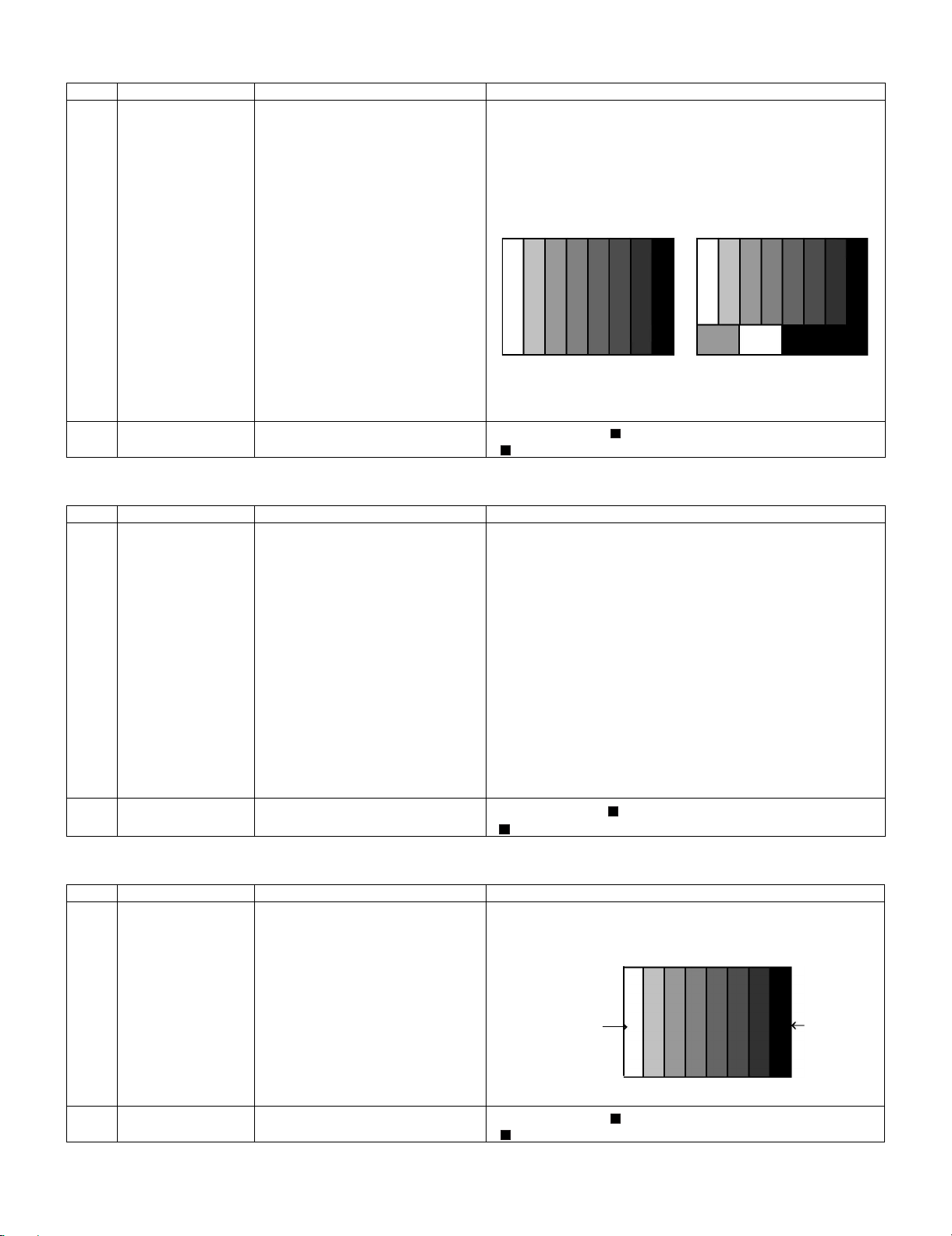
㸡100% white
5 – 14
Page 30
LC-26SA1E/RU, LC-32SA1E/RU
5. PAL signal & tuner adjustment
Adjustment point Adjustment Conditions Adjustment procedure
1 Setting [Signal]
PAL
Full Field Color Bar
Composite or RF signal
[Terminal]
EXT3 VIDEO IN
TUNER
•Feed the PAL full field colour bar signal (75% colour saturation) to
EXT3 VIDEO IN.
•Feed the RF signal (PAL colour bar) to TUNER.
•Make sure the PAL colour bar pattern has the sync level of 7:3 with
the picture level.
㪲VIDEO IN SIGNAL]
[RF Signal]
㸡100% white
2 Auto adjustment
performance
Adjustment process
Page3
Bring the cursor on [ PAL + TUNER ADJ] and press [OK]
[ PAL + TUNER ADJ OK] appears when finished.
6. PAL Signal & Tuner Adjustment (SMPTE RF SIGNAL-Alternative Method)
Adjustment point Adjustment Conditions Adjustment procedure
1 Setting [Signal]
PAL
Full Field Color Bar
Composite or RF SMPTE signal
[Terminal]
EXT3 VIDEO IN
TUNER
2 Auto adjustment
performance
Adjustment process
Page6
•Feed the PAL full field color bar signal (75% color saturation) to EXT3
VIDEO IN
•Feed the RF signal SMPTE color bar (E-12) to TUNER.
•Make sure the SMPTE color bar pattern (E-12) has the sync level of
7:3 with the picture level.
Bring the cursor on [ PAL +TUNER ADJ] and press [OK].
[ PAL+ TUNER ADJ OK] appears when finished.
㸡100% white
7. ADC adjustment (Component 15K)
Adjustment point Adjustment Conditions Adjustment procedure
1 Setting [Signal]
COMP15K, 50Hz
100% Full Field Colour Bar
[Terminal]
EXT4 COMPONENT IN
2 Auto adjustment
performance
Adjustment process
Page4
•Feed the COMPONENT 15K 100% full field colour bar signal (100%
colour saturation) to EXT4 COMPONENT IN.
100% white
Bring the cursor on [ COMP15K ADJ] and press [OK]
[ COMP15K ADJ OK] appears when finished.
5 – 15
Black
Page 31

LC-26SA1E/RU, LC-32SA1E/RU
[8] White Balance Adjustment
Adjustment gradation values (IN) appear on page 7/11 of process adjustment, and adjustment initial values (offset value) appear on pages 8/11 and
9/11. For white balance adjustment, adjust the offset values on pages 8/11 and 9/11.
[Condition of the unit for inspection] Modulated light: MAX (+8)
[Adjustment reference device] Minolta CA-210
[Adjustment]
Check that the values on page 7/11 of process adjustment are set as below. If not, change them accordingly.
M GAMMA IN 1 160 M GAMMA IN 2 320
M GAMMA IN 3 480 M GAMMA IN 4 640
M GAMMA IN 5 800 M GAMMA IN 6 960
1) Display the current adjustment status at point 6. (Page 8/11 of process adjustment)
The display for checking the adjustment status is toggled by pressing the “6” button on the remote control.
(Normal OSD display → “6”→ display for check (OSD disappears) → “6” →normal OSD display → • • •)
2) Read the value of the luminance meter.
3) Change M GAMMA R6/M GAMMA B6 (Adjustment offset value) on page 9/11 of process adjustment so that the values of the luminance meter
approach x =0.272 and y =0.277.
(Basically, G is not changed. If adjustment fails with R and B, change G. When G is lowered, the weaker of R and B must be fixed.)
4) If G is changed in step 3), change the values of M GAMMA G1- M GAMMA G5 on pages 8/11 and 9/11 of process adjustment as follows. When
not changed, go to step5).
Offset value of M GAMMA G1 = (Offset value of M GAMMA G6) * (160/960)
Offset value of M GAMMA G2 = (Offset value of M GAMMA G6) * (320/960)
Offset value of M GAMMA G3 = (Offset value of M GAMMA G6) * (480/960)
Offset value of M GAMMA G4 = (Offset value of M GAMMA G6) * (640/960)
Offset value of M GAMMA G5 = (Offset value of M GAMMA G6) * (800/960)
5) Display the adjustment status of the current point 5. (Each time the “5” button on the remote control is pressed, the adjustment status check display is toggled.)
(Normal OSD display → “5” → Check display (OSD disappears) → “5” → Normal OSD display → • • •)
Change M GAMMA R5/M GAMMA B5 (adjustment offset value) on page 9/11 of process adjustment so that the values of the luminance meter
approach x = 0.272 and y = 0.277.
6) Repeat step 5) for points 4, 3, 2, and 1.
5 – 16
Page 32

LC-26SA1E/RU, LC-32SA1E/RU
[9] QS Temperature NVM Data Confirmation
During servicing of the LCD TV set , by software upgrading or by any cleaning NVM, itÅfs mandatory select the ÅgInch SettingÅh in Service Mode,
Page 2, according to the size of the TV set.
[10] Initialization to factory settings
Caution: When the factory settings have been made, all user setting data, including the channel settings, are initialized. (The adjust-
ments done in the adjustment process mode are not initialized.) Keep this in mind when initializing these settings.
Adjustment item Adjustment conditions Adjustment procedure
1 Factory settings Forcibly turn off the power
(See to below caution)
After adjustments, exit the adjustment process mode.
To exit the adjustment process mode, unplug the AC power cord from the outlet to forcibly turn off the power.
When the power is turned off with the remoto control, unpulug the AC power cord and plug it back in.
•Enter the adjustment process mode.
•Move the cursor to [Factory Init] on page 2/11.
•Use the R/C key to select a region from [EURO/UK/ITALY/
FRANCE/RUSSIA]and press the [OK] key.
“EXECUTING” appears and initialization starts.
After a while,”***OK***” appears and the setting is complete.
Note: Never turn the power off during initialization.
•The following items are initialized in the factory setting.
1. User settings
2. Channel data (e.g. broadcast frequencies)
3. Password data
5 – 17
Page 33

LC-26SA1E/RU, LC-32SA1E/RU
[1 1] Lamp error detection
1. Functional description
This LCD colour television has a function (lamp error detection) to be turned OFF automatically (Inverter unit) for safety when the lamp or lamp circuit
is abnormal.
If the lamp or lamp circuit is abnormal, or some other errors happen, and the lamp error detection is executed, the following occur.The Inverter circuit
stops but the rest of TV continues working. The power led is green.
2. Countermeasures
Proceed to repair the inverter unit to solve the problem that produces the lamp error.
3. Reset standby cause error list
For 26/32” this is not necessary because the lamp error detection is not operative by software.
[12] Public Mode (Hotel Mode)
1. How to Enter in the Public Mode (Hotel Mode).
Turn on the power and enter in the Adjustment Process mode (ADJ1 or Service Mode) as usual.
In the [INIT], Page 2/11 of Service, turns ON the Public Mode option.
Turn off TV by pressing Main Power switch.
While pressing “VOL+” and “P^” keys at the same time, press Main Power switch for more than 2 seconds.
After this sequence the TV will turn on showing the Public Mode setting screen as follows:
Is possible to select each item of function by pressing cursor UP/DOWN keys on the remote control or CH( )( ) keys on the LCD TV.
The setting position of each item of functions is made by pressing cursor RIGHT/LEFT keys on the remote control or VOL(+)(-) keys on the LCD TV.
Select EXECUTE position after you set all function, and press cursor RIGHT/LEFT keys on the remote control or VOL(+)/(-) keys on the LCD TV for
confirmation.
2. Public Mode Settings.
1. POWER ON FIXED [VARIABLE ↔ FIXED]
When it is set to “FIXED” the TV is impossible to be switch off by Main Switch or Remote Control.
2. MAXIMUM VOLUME [0 ↔ 60]
Is possible to set the maximum volume at limited level.
3. VOLUME FIXED [VARIABLE ↔ FIXED]
Is possible to fix the sound volume at limited level.
When “FIXED” is selected the sound volume before limited is fixed.
4. VOLUME FIXED LEVEL [0 ↔ 60]
If “FIXED” has been selected, is possible to set a fixed volume at the level that is chosen.
5. RC BUTTON [RESPOND ↔ NO RESPOND]
If “NO RESPOND” is selected, the remote control keys are inoperative.
6. PANEL BUTTON [RESPOND ↔ NO RESPOND]
If “NO RESPOND” has been selected, the set’s keys remain deactivated (Except POWER key).
7. MENU BUTTON [RESPOND ↔ NO RESPOND]
5 – 18
Page 34

LC-26SA1E/RU, LC-32SA1E/RU
If “NO RESPOND” has been selected, “MENU” key, of remote control, is inoperative.
8. ON SCREEN DISPLAY [YES ↔ NO]
If “NO” has been selected, the On Screen Display does not appear.
9. INPUT MODE START [ NORMAL → TV (X) → INPUT1 → INPUT2 → INPUT3 → INPUT4 → INPUT5 ]
When any other item than “NORMAL” has been selected, the sets will start in a selected input mode at the next power-on.
10.INPUT MODE FIXED [VARIABLE → FIXED]
“FIXED” has been selected, any channels and input modes other than those selected at the start mode cannot be picked up.
11.RESET
Cancel all Public Mode settings. (It returns to the factory settings)
12.EXECUTE
Select this item, and press cursor RIGHT/LEFT keys on the remote control or VOL(+)/(-) keys on the LCD TV for confirmation the functions set-
tings.
5 – 19
Page 35

LC-26SA1E/RU, LC-32SA1E/RU
LC-26SA1E
CHAPTER 6. TROUBLESHOOTING TABLE
Service Manual
[1] TROBLESHOOTING TABLE
Power unit operation check.
Are the power cord and harness in the unit properly connected? NO Connect the power cord and harness properly, and turn on the
power.
YES
Is F701 normal? NO Are both ends of C704, C707 (26) and C705 (32) short-circuited
when checking their resistance values?
NO
Replace F701.
YES
Is a voltage of BU5V applied to pin (20) of P701?
(Set the main power SW to OFF.)
NO
Is a voltage of approx.
8 - 15V to pin (4) of
IC705?
YES
Check short circuit of 5V line (D737,
C752, etc.).
YES
Is it a symptom that the relay clatters twice as soon as the main
power SW is set to ON and the power is not supplied?
YES
Does the same symptom appear even if R858 (2.7k) is
removed and the power is supplied again?
YES
Check Q724, D731, D734, IC707, D751, D753, D754,
D741, D759 and D746.
C704 ••• Check VA701, VA702 and D701.
C707 (26)/C705 (32) ••• Check IC704 and 705.
NO Check IC705, IC708, D725 and Q724.
Check IC704, D728, D762 and D736. If there are no problems,
NO
check the resistance value between pins (1) and (6) of P704.
When the value is low (several Ω - several hundred Ω),
disconnect P704. If the value is still low, the parts of 24V line are
defective. When the resistance value is several kΩ, check the
inverter unit.
YES
NO
Does a relay noise sound? (Once) NO Are PCON1 and 2 [pins (1) and (2) of P702] at Hi (3V or more)?
YES YES
Check peripheral circuits of D738, R828 and D735. Check peripheral circuits of Q712, Q713, Q721, Q723
and RY701.
There is a possibility that control by P-CON is not performed
properly. Check whether the “PS-ON” and “PS-ON2” signals are
sent from pins (97) and (91) of IC1710 (FPGA) of MAIN-UNIT.
NO
6 – 1
Page 36

LC-26SA1E/RU, LC-32SA1E/RU
No sound (1) (during the reception of TV broadcasting)
No audio output during UHF/VHF reception
Checklist;
1) Is the volume set to MIN or MUTE on the remote control? ••• Set the desired volume.
2) Are headphones connected to HEADPHONE (J1301)? ••• Disconnect them.
3) Is ANT-CABLE disconnected or connected improperly? ••• Connect it correctly as per the operation manual.
Is the audio signal (L/R)
sent from pins (28) and
(27) of IC3002 (VCT)?
(AV-UNIT) YES NO
Is the audio signal of pins
(3) and (5) of IC303
(OP-AMP) sent properly?
YES (TUNER) NO
Is the audio signal of pin
(4) Of IC301/IC302
(AUDIO-AMP) sent
properly?
NO Check IC303 or
NO Check HEAD-PHONE
NO
peripheral circuits.
(J1301) or peripheral
circuits.
Is the SIF signal (SIF_IN+)
sent to pin (31) of IC3002
(VCT)?
Is the audio signal (SIF)
sent from pin (1) of
CONNECTOR (SC2705)?
Is the audio signal (SIF)
sent from pin (12) of IC201
(IF-DEMOD)?
Check whether +5V and
YES
YES Check pin (31) of IC3002
YES Check Q203 (AMP) and
+8V are supplied to pins
(33) and (18) of IC3002
respectively. Or, check
peripheral circuits.
(VCT) and peripheral
circuits.
peripheral circuits.
YES NO
Is the audio signal output
of pins (2) and (4) of P301
(AUDIO-CONNECTOR)
normal?
YES NO
Check Speaker (right and
left) and wire harness.
Check whether 33V and
NO Check P301 (AUDIO-
CONNECTOR) and
peripheral circuits.
Is the SIF signal sent to
pins (23) and (24) of IC201
(IF-DEMOD)?
Is the IF signal sent from
pin (11) of TUNER
(TU201)?
NO
5V are supplied to pins (9)
and (7) of TUNER (TU201)
respectively. Check SDA/
SCL and AGC signal.
YES Check IC201 and
peripheral circuits.
YES Check FL202 and
peripheral circuits.
YES Replace TUNER (TU201).
6 – 2
Page 37

No sound from external input devices (2)
No sound from an external input device connected to EXT1
(SCART1).
<EXT1>
Is IN1-L audio signal sent from pin (6) of SCART1 terminal
(J1101) to pin (14) of IC3002 (VCT)?
Is IN1-R audio signal sent from pin (2) of SCART1 terminal
(J1101) to pin (13) of IC3002 (VCT)?
YES
Is the audio signal properly sent from pins (28) and (27) of
IC3002?
YES
Is the audio signal of pins (1) and (7) of IC303 (OP-AMP) sent
properly?
YES
Is the audio output signal of pins (13) and (16) of IC302/IC301
(MAIN-AMP) normal?
LC-26SA1E/RU, LC-32SA1E/RU
NO Check pins (6) and (2) of SCART1 and connection to an external
input device.
NO Check IC3002 or peripheral circuits.
NO Check IC303 or peripheral circuits.
NO Check IC302/IC301 (MAIN-AMP), HEADPHONE and peripheral
circuits.
YES
Check CONNECTOR (P301) and Speaker (right and left).
No sound from external input devices (2)
No sound from an external input device connected to EXT2
(SCART2).
<EXT2>
Is IN2-L audio signal sent from pin (27) of SCART2 terminal
(J1101) to pin (12) of IC3002 (VCT)?
Is IN2-R audio signal sent from pin (23) of SCART2 terminal
(J1101) to pin (11) of IC3002 (VCT)?
YES
Is the audio signal properly sent from pins (28) and (27) of
IC3002?
YES
Is the audio signal of pins (1) and (7) of IC303 (OP-AMP) sent
properly?
NO Check pins (27) and (23) of SCART2 and connection to an
external input device.
NO Check IC3002 or peripheral circuits.
NO Check IC303 or peripheral circuits.
YES
Is the audio output signal of pins (13) and (16) of IC302/IC301
(MAIN-AMP) normal?
YES
Check CONNECTOR (P301) and Speaker (right and left).
NO Check IC302/IC301 (MAIN-AMP), HEADPHONE and peripheral
circuits.
6 – 3
Page 38

LC-26SA1E/RU, LC-32SA1E/RU
No sound from external input devices (2)
No sound from an external input device connected to EXT3.
<EXT3>
Is IN3-L audio signal sent from pin (3) of J1201 terminal to pin
(16) of IC3002?
Is IN3-R audio signal sent from pin (5) of J1201 terminal to pin
(15) of IC3002?
YES
Is the audio signal properly sent from pins (28) and (27) of
IC3002?
YES
Is the audio signal of pins (1) and (7) of IC303 (OP-AMP) sent
properly?
YES
Is the audio output signal of pins (13) and (16) of IC302/IC301
(MAIN-AMP) normal?
NO Check pins (3) (J1201) and (5) (J1201) of EXT3 and connection
to an external input device.
NO Check IC3002 or peripheral circuits.
NO Check IC303 or peripheral circuits.
NO Check IC302/IC301 (MAIN-AMP), HEADPHONE and peripheral
circuits.
YES
Check CONNECTOR (P301) and Speaker (right and left).
No sound from external input devices (2)
No sound from EXT4 (AUDIO) connecting an external input
device.
<EXT4>
Is D-SUB-L audio signal sent from J2702 to pin (15) of IC2704?
Is D-SUB-R audio signal sent from J2702 to pin (2) of IC2704?
YES
Is D-SUB-L audio signal sent to pin (10) of IC3002?
Is D-SUB-R audio signal sent to pin (9) of IC3002?
YES
Is the audio signal properly sent from pins (28) and (27) of
IC3002?
YES
Is the audio signal of pins (1) and (7) of IC303 (OP-AMP) sent
properly?
NO Check IC3002 or peripheral circuits.
NO Check IC303 or peripheral circuits.
YES
Is the audio output signal of pins (13) and (16) of IC302/IC301
(MAIN-AMP) normal?
YES
Check CONNECTOR (P301) and Speaker (right and left).
NO Check IC302/IC301 (MAIN-AMP), HEADPHONE and peripheral
circuits.
6 – 4
Page 39

No sound from external input devices (2)
No sound from EXT5 (AUDIO) connecting an external input
device.
<EXT5>
Is HDMI-L audio signal sent from J2701 to pin (14) of IC2704?
Is HDMI-R audio signal sent from J2701 to pin (5) of IC2704?
YES
Is HDMI-L audio signal sent to pin (10) of IC3002?
Is HDMI-R audio signal sent to pin (9) of IC3002?
YES
Check that Option-HDMI Setup-Audio select is set to “Analog”.
OK
Is the audio signal properly sent from pins (28) and (27) of
IC3002?
YES
Is the audio signal of pins (1) and (7) of IC303 (OP-AMP) sent
properly?
LC-26SA1E/RU, LC-32SA1E/RU
NO Check output of pins (13) and (3) of IC2704 and peripheral
circuits.
NO Check IC3002 or peripheral circuits.
NO Check IC303 or peripheral circuits.
YES
Is the audio output signal of pins (13) and (16) of IC302/IC301
(MAIN-AMP) normal?
YES
Check CONNECTOR (P301) and Speaker (right and left).
No sound except from speakers (3)
No audio output from the headphones.
Is there audio output on pins (2) and (3) of the headphone
terminal (J1301)?
NO
Is audio input/output signal of pins (3) and (5)/(1) and (7) of IC303
(OP-AMP) normal?
NO
Is audio output signal (SPK-OUT L/R) properly sent from pins
(28) and (27) of IC3002 (VCT)?
NO
Check audio input signal of pin (31) of IC3002 (VCT), pins (18)
and (33) of the power line, pins (84) and (83) of I2C-LINE, and
peripheral circuits.
NO Check IC302/IC301 (MAIN-AMP), HEADPHONE and peripheral
circuits.
6 – 5
Page 40

LC-26SA1E/RU, LC-32SA1E/RU
No sound except from speakers (3)
No audio output from EXT1 (SCART) terminal.
Checklist:
1) Is the MUTE button on the remote control set to ON? ••• Set to OFF.
2) Check the connection to external devices. ••• Is there any improper connection?
Is audio signal sent to pins (3) and (1) of EXT1 (J1101)? YES Check the connection to EXT1 (J1101) and external devices.
NO
Is S-MUTE-LINE [IC1710 (pin 100)] at H?
(Check Q1106/Q1105 operation.)
NO
Is audio signal sent from pins (24) and (23) of IC3002? NO Check the power supply 8/5 V pins (18) and (33) of IC3002 and
peripheral circuits.
YES
Check the audio signal output line from pins (24) and (23) of
IC3002 to pins (3) and (1) of EXT1.
No sound except from speakers (3)
No audio output from EXT2 (SCART) terminal.
Checklist:
1) Is the MUTE button on the remote control set to ON? ••• Set to OFF.
2) Check the connection to external devices. ••• Is there any improper connection?
Is audio signal sent to pins (24) and (22) of EXT2 (J1101)? YES Check the connection to EXT2 (J1101) and external devices.
NO
Is S-MUTE-LINE [IC1710 (pin 100)] or S2-MUTE-LINE [IC3003
(pin 26)] at H? (Check Q1102/Q1101 operation.)
NO
Is audio signal sent from pins (22) and (21) of IC3002? NO Check the power supply 8/5 V pins (18) and (33) of IC3002 and
peripheral circuits.
YES
Check the audio signal output line from pins (22) and (21) of
IC3002 to Q1103/Q1104/Q1201/Q1202.
6 – 6
Page 41

LC-26SA1E/RU, LC-32SA1E/RU
No sound except from speakers (3)
No audio output from AUDIO OUTPUT terminal.
Checklist:
1) Is the MUTE button on the remote control set to ON? ••• Set to OFF.
2) Check the connection to external devices. ••• Is there any improper connection?
Is audio signal sent to pins (13) and (15) [L/R (white) (red)] of
AUDIO OUTPUT terminal (J1201)?
NO
Is S-MUTE-LINE [IC1710 (pin 100)] at H?
(Check Q1204/Q1203 operation.)
NO
Is audio signal sent from pins (22) and (21) of IC3002? NO Check the power supply 8/5 V pins (18) and (33) of IC3002 and
YES
Check the audio signal output line from pins (22) and (21) of
IC3002 to Q1103/Q1104/Q1201/Q1202.
YES Check the connection to AUDIO OUTPUT terminal (J1201) and
external devices.
peripheral circuits.
6 – 7
Page 42

LC-26SA1E/RU, LC-32SA1E/RU
<On input of the tuner (U/V)> No picture on the display (1)
No picture appears on LCD during the tuner (U/V) reception.
Checklist:
1) Is “INPUT SOURCE” button on the remote control set up correctly? ••• See the operation manual and set “INPUT SOURCE” to “TV”.
2) Is MENU-PICTURE-Contrast/Brightness set to “MIN”? ••• Set it to an appropriate level.
3) Is ANT-CABLE disconnected or connected improperly? ••• Connect it correctly as per the operation manual.
YES
Is level of pins (4) and (5) of tuner (TU201) and pins (10) and (11)
of IC201 (IF-DEMOD) at H?
YES
Is the video signal (IF) sent from pin (11) of tuner (TU201)? NO Check the tuner (TU201) and peripheral circuits.
YES
Is video signal sent from pin (17) of IC201 (IF-DEMOD)? NO Check FL201 (SAW-FIL), IC201 and peripheral circuits.
YES
Is the video signal VIN1 (ATUNER-CVBS) sent to pin (191) of
lC3002 (VCT)?
NO These are communications lines for control (I2C). Follow the
path and check whether they are forced to L (PULL_DOWN).
NO Check IC201 (IF-DEMOD), CONNECTOR (P201 /SC2705) and
peripheral circuits.
YES
Is LVDS video signal (LVDS_0N/0P-3N/3P) sent to pins (141)/
(140) - (129)/(128) of IC3002 (VCTP), and is CLK signal
(LVDS_CN/CP) sent to pins (132)/(131)?
YES
Is LVDS video signal (LVDS_0N/0P-3N/3P) sent to pins (12)/(13)
-(24)/(25) of CONNECTOR CN1 of LCD-CONT-UNIT, and is CLK
signal (LVDS_CN/CP) sent to pins (21)/(22)?
YES
Is power (LCD5V) supplied to pins (2) - (5) of CONNECTOR CN1
in LCD-CONT-UNIT?
YES
Replace LCD-CONT-UNIT.
NO Check pins (192)/(170)/(133) of BU3.3V line of IC3002 (VCTP),
pins (185)/(169)/(142) of 1.8V line and peripheral circuits.
NO Check CONNECTOR (P2305, CN1) and HARNESS WIRE (LV).
NO Is LCD5V supplied to pins (31) - (28) of CONNECTOR (P2305)?
Check HARNESS WIRE (LV).
6 – 8
Page 43

LC-26SA1E/RU, LC-32SA1E/RU
<During external connection> No picture on the monitor (2)
SCART1:
No picture appears on EXT1 - connected monitor during the tuner
(U/V) reception.
Checklist:
1) Are input terminal on back of TV and “INPUT SOURCE” button on the remote control set up correctly? ••• See the operation manual and
set “INPUT SOURCE” appropriately.
2) Is the Signal Type (item) in MENU-Option-Input Select equal to Signal Type of an external device? ••• Set it to “CVBS”, “Y/C” or “RGB”.
3) Is ANT-CABLE disconnected or connected improperly? ••• Connect it correctly as per the operation manual.
4) The picture is sent to the monitor in a CVBS signal if the source during display is TV, CVBS or Y/C of EXT1-3.
When sent by component, etc., that signal is not sent to the monitor.
5) When the monitor picture is not sent and is not displayed on the monitor, refer to “No picture” for each terminal.
6) The video output from EXT1 is not the monitor output (output of the picture now watching).
The picture of the last selected TV channel is always sent to EXT1. (Specification)
Is video signal sent to pin (19) of SCART1 (J1101)? YES Check SCART1, external connection or input setting.
NO
Is video signal (V-OUT1) sent from pin (2) of IC1102 (SW)? YES Check SCART1 (J1101) and peripheral circuits.
NO
Is video signal (V-OUT1) sent from pin (195) of IC3002 (VCT)? YES Check IC1102 (SW), Connector (P1 101, SC2702) and peripheral
circuits.
NO
Is video signal (CVBS) sent to pin (191) of lC3002 (VCT)? YES Check power supply of IC3002 (VCT) and peripheral circuits.
NO
Is video signal (CVBS) sent from pin (17) of IC201 (IF-DEMOD)? YES Check CONNECTOR (P201, SC2705) and peripheral circuits.
NO
Is video signal (IF) sent from pin (11) of tuner (TU201)? YES Check IC201, FL201 (SAW-FIL), Q202 and peripheral circuits.
NO
Check 5/35 V power supply pins (7) and (9), I2C line pins (5) and
(4) of tuner (TU201) and peripheral circuits.
6 – 9
Page 44

LC-26SA1E/RU, LC-32SA1E/RU
<During external connection> No picture on the monitor (2)
SCART2:
No picture from EXT1 appears on EXT2-connected monitor.
NOTE: Normally, if the screen during display is sent to EXT2, no
picture is sent to EXT2.
Checklist:
1) Are input terminal on back of TV and “INPUT SOURCE” button on the remote control set up correctly? ••• See the operation manual and
set “INPUT SOURCE” appropriately.
2) Is the Signal Type (item) in MENU-Option-Input Select equal to Signal Type of an external device? ••• Set it to “CVBS”, “Y/C” or “RGB”.
3) Is ANT-CABLE disconnected or connected improperly? ••• Connect it correctly as per the operation manual.
4) The picture is sent to the monitor in a CVBS signal if the source during display is TV, CVBS or Y/C of EXT1-3.
When sent by component, etc., that signal is not sent to the monitor.
5) When the monitor picture is not sent and is not displayed on the monitor, refer to “No picture” for each terminal.
6) The video output from EXT1 is not the monitor output (output of the picture now watching).
The picture of the last selected TV channel is always sent to EXT1. (Specification)
Is video signal sent to pin (40) of SCART2 (J1101)? YES Check SCART2, external connection or input setting.
NO
Is video signal (V-OUT2) sent from pin (2) of IC1101 (SW)? YES Check SCART2 (J1101) and peripheral circuits.
NO
Is video signal (V-OUT2) sent from pin (194) of IC3002 (VCT)? YES Check IC1101 (SW), Connector (P1 102, SC2703) and peripheral
NO
Is video signal (VIN1) from EXT1 sent to pin (190) of IC3002
(VCT)?
NO
Check whether video signal is sent to pin (20) of SCART1. YES Check SCART1, IC2702 (SW), CONNECTOR (SC2702, P1101)
NO
Check SCART1, external connection or input setting.
YES Check power supply of IC3002 (VCT) and peripheral circuits.
circuits.
and peripheral circuits.
6 – 10
Page 45

LC-26SA1E/RU, LC-32SA1E/RU
<During external connection> No picture on the monitor (2)
SCART2:
No picture from EXT3 appears on EXT2- connected monitor.
Checklist:
1) Are input terminal on back of TV and “INPUT SOURCE” button on the remote control set up correctly? ••• See the operation manual and
set “INPUT SOURCE” appropriately.
2) Is the Signal Type (item) in MENU-Option-Input Select equal to Signal Type of an external device? ••• Set it to “CVBS”, “Y/C” or “RGB”.
3) Is ANT-CABLE disconnected or connected improperly? ••• Connect it correctly as per the operation manual.
4) The picture is sent to the monitor in a CVBS signal if the source during display is TV, CVBS or Y/C of EXT1-3.
When sent by component, etc., that signal is not sent to the monitor.
5) When the monitor picture is not sent and is not displayed on the monitor, refer to “No picture” for each terminal.
6) The video output from EXT1 is not the monitor output (output of the picture now watching).
The picture of the last selected TV channel is always sent to EXT1. (Specification)
Is video signal sent to pin (40) of SCART2 (J1101)? YES Check SCART2, external connection or input setting.
NO
Is video signal (V-OUT2) sent from pin (2) of IC1101 (SW)? YES Check SCART2 (J1101) and peripheral circuits.
NO
Is video signal (V-OUT2) sent from pin (194) of IC3002
(VCT)?
NO
Is video signal (VIN7) from EXT3 sent to pin (184) of IC3002
(VCT)?
NO
Is video signal (IN3YV) sent to pin (2) of IC1201 (SW)? YES Check pin (184) of IC3002 (VCT), CONNECTOR (SC2703,
NO
Is video signal (CVBS) sent from pin (1) of A/V-TERMINAL
(J1201=EXT3)?
NO
Check A/V-TERMINAL (J1201), external connection or input
setting.
YES Check IC1101 (SW), Connector (P1 102, SC2703) and peripheral
circuits.
YES Check power supply of IC3002 (VCT) and peripheral circuits.
P1102) and peripheral circuits.
YES Check pin (1) (IN3SW) of IC1201 (SW), power supply and
peripheral circuits.
6 – 11
Page 46

LC-26SA1E/RU, LC-32SA1E/RU
<When EXT1 is used for external input> No picture on the display (3)
No EXT1-Composite output of the external input system.
Checklist:
1) Is “INPUT SOURCE” button on the remote control set up correctly? ••• See the operation manual and set “INPUT SOURCE” to “EXIT”.
2) Is MENU-PICTURE-CONTRAST/BRIGHTNESS set to “MIN”? ••• Set it to an appropriate level.
3) Check the connection to the external device ••• Connect it correctly as per the operation manual for the device.
Is composite video signal sent to pin (20) of SCART1 (J1101)? NO Check external connection, input setting, SCART1 and
YES
Is composite video signal (VIN_1) sent to input terminal pin (6) of
IC2702 (SW)?
YES
Is composite video signal (CVBS1=VIN2) sent to input terminal
pin (190) of IC3002 (VCT)?
YES
Is LVDS signal (LVDS_0N/0P-3N/3P) sent from pins (141) and
(140) - (129) and (128) of IC3002 (VCTP), and is CLK signal
(LVDS_CN/CP) sent from pins (132) and (131)?
NO Check CONNECTOR (SC2702/P1101), SCART1 (J1101) and
NO Check IC2702 (SW) and peripheral circuits.
NO Check pins (192), (170) and (133) of BU3.3V power line and pins
peripheral circuits.
peripheral circuits.
(185), (169) and (142) of BU1.8V power line of IC3002 (VCTP),
and peripheral circuits.
YES
Is LVDS signal (LVDS_0N/0P-3N/3P) sent to pins (12) and (13) -
(24) and (25) of CONNECTOR CN1 in LCD-CONT-UNIT, and is
CLK signal (LVDS_CN/CP) sent to pins (21) and (22)?
YES
Is power (LCD5V) supplied to pins (2) - (5) of CONNECTOR CN1
in LCD-CONT-UNIT?
YES
Replace LCD-CONT-UNIT.
NO Check CONNECTOR (P2305, CN1) and HARNESS WIRE (LV).
NO Is LCD5V supplied to pins (31) - (28) of CONNECTOR (P2305)?
Check HARNESS WIRE (LV).
6 – 12
Page 47

LC-26SA1E/RU, LC-32SA1E/RU
<When EXT1 is used for external input> No picture on the display (3)
No EXT1-RGB output of the external input system.
Checklist:
1) Is “INPUT SOURCE” button on the remote control set up correctly? ••• See the operation manual and set “INPUT SOURCE” to “EXIT”.
2) Is MENU-PICTURE-CONTRAST/BRIGHTNESS set to “MIN”? ••• Set it to an appropriate level.
3) Check the connection to the external device ••• Connect it correctly as per the operation manual for the device.
Is RGB signal sent to pins (15),(11) and (7) of SCART1 (J1101)? NO Check external connection, input setting, SCART1 (J1101) and
peripheral circuits.
YES
Is RGB signal (R1/G1/B1=VIN_6/5/9) sent to input terminal pins
(187), (175) and (182) of IC3002 (VCT)?
YES
Is LVDS signal (LVDS_0N/0P-3N/3P) sent from pins (141) and
(140) - (129) and (128) of IC3002 (VCTP), and is CLK signal
(LVDS_CN/CP) sent from pins (132) and (131)?
NO Check CONNECTOR (SC2702/P1101), SCART1 (J1101) and
peripheral circuits.
NO Check pins (192), (170) and (133) of BU3.3V power line and pins
(185), (169) and (142) of BU1.8V power line of IC3002 (VCTP),
and peripheral circuits.
YES
Is LVDS signal (LVDS_0N/0P-3N/3P) sent to pins (12) and (13) (24) and (25) of CONNECTOR CN1 in LCD-CONT-UNIT, and is
CLK signal (LVDS_CN/CP) sent to pins (21) and (22)?
YES
Is power (LCD5V) supplied to pins (2) - (5) of CONNECTOR CN1
in LCD-CONT-UNIT?
YES
Replace LCD-CONT-UNIT.
NO Check CONNECTOR (P2305, CN1) and HARNESS WIRE (LV).
NO Is LCD5V supplied to pins (31) - (28) of CONNECTOR (P2305)?
Check HARNESS WIRE (LV).
6 – 13
Page 48

LC-26SA1E/RU, LC-32SA1E/RU
<When EXT1 is used for external input> No picture on the display (3)
No EXT1-Y/C output of the external input system.
Checklist:
1) Is “INPUT SOURCE” button on the remote control set up correctly? ••• See the operation manual and set “INPUT SOURCE” to “EXIT”.
2) Is MENU-PICTURE-CONTRAST/BRIGHTNESS set to “MIN”? ••• Set it to an appropriate level.
3) Check the connection to the external device ••• Connect it correctly as per the operation manual for the device.
Is Y/C signal sent to pins (20) and (15) of SCART1 (J1101)? NO Check external connection, input setting, SCART1 (J1101) and
YES
Is Y/C signal (VIN1=Y1/C1) sent to input terminal pins (190) and
(187) of IC3002 (VCT)?
YES
Is LVDS signal (LVDS_0N/0P-3N/3P) sent from pins (141) and
(140) - (129) and (128) of IC3002 (VCTP), and is CLK signal
(LVDS_CN/CP) sent from pins (132) and (131)?
YES
Is LVDS signal (LVDS_0N/0P-3N/3P) sent to pins (12) and (13) (24) and (25) of CONNECTOR CN1 in LCD-CONT-UNIT, and is
CLK signal (LVDS_CN/CP) sent to pins (21) and (22)?
NO Check CONNECTOR (SC2702/P1101), SCART1 (J1101) and
NO Check pins (192), (170) and (133) of BU3.3V power line and pins
NO Check CONNECTOR (P2305, CN1) and HARNESS WIRE (LV).
peripheral circuits.
peripheral circuits.
(185), (169) and (142) of BU1.8V power line of IC3002 (VCTP),
and peripheral circuits.
YES
Is power (LCD5V) supplied to pins (2) - (5) of CONNECTOR CN1
in LCD-CONT-UNIT?
YES
Replace LCD-CONT-UNIT.
NO Is LCD5V supplied to pins (31) - (28) of CONNECTOR (P2305)?
Check HARNESS WIRE (LV).
6 – 14
Page 49

LC-26SA1E/RU, LC-32SA1E/RU
<When EXT2 is used for external input> No picture on the display (4)
No EXT2-Composite output of the external input system.
Checklist:
1) Is “INPUT SOURCE” button on the remote control set up correctly? ••• See the operation manual and set “INPUT SOURCE” to “EXT2”.
2) Is MENU-PICTURE-CONTRAST/BRIGHTNESS set to “MIN”? ••• Set it to an appropriate level.
3) Check the connection to the external device ••• Connect it correctly as per the operation manual for the device.
Is composite video signal sent to pin (41) of SCART2 (J1101)? NO Check external connection, input setting, SCART2 (J1101) and
peripheral circuits.
YES
Is composite video signal (VIN-2) sent to input terminal pin (4) of
IC2702 (SW)?
YES
Is composite video signal (CVBS2=VIN2) sent to input terminal
pin (190) of IC3002 (VCT)?
YES
Is LVDS signal (LVDS_0N/0P-3N/3P) sent from pins (141) and
(140) - (129) and (128) of IC3002 (VCTP), and is CLK signal
(LVDS_CN/CP) sent from pins (132) and (131)?
NO Check CONNECTOR (SC2702/Pl101), SCART2 (J1101) and
peripheral circuits.
NO Check IC2702 (SW) and peripheral circuits.
NO Check pins (192), (170) and (133) of BU 3.3V power line and
pins (185), (169) and (142) of BU1.8V power line of IC3002
(VCTP), and peripheral circuits.
YES
Is LVDS signal (LVDS_0N/0P-3N/3P) sent to pins (12) and (13) (24) and (25) of CONNECTOR CN1 in LCD-CONT-UNIT, and is
CLK signal (LVDS_CN/CP) sent to pins (21) and (22)?
YES
Is power (LCD5V) supplied to pins (2) - (5) of CONNECTOR CN1
in LCD-CONT-UNIT?
YES
Replace LCD-CONT-UNIT.
NO Check CONNECTOR (P2305, CN1) and HARNESS WIRE (LV).
NO Is LCD5V supplied to pins (31) - (28) of CONNECTOR (P2305)?
Check HARNESS WIRE (LV).
6 – 15
Page 50

LC-26SA1E/RU, LC-32SA1E/RU
<When EXT2 is used for external input> No picture on the display (4)
No EXT2-RGB output of the external input system.
Checklist:
1) Is “INPUT SOURCE” button on the remote control set up correctly? ••• See the operation manual and set “INPUT SOURCE” to “EXT2”.
2) Is MENU-PICTURE-CONTRAST/BRIGHTNESS set to “MIN”? ••• Set it to an appropriate level.
3) Check the connection to the external device ••• Connect it correctly as per the operation manual for the device.
Is RGB signal sent to pins (36), (32) and (28) of SCART2
(J1101)?
YES
Is RGB signal (R2/G2/B2=VIN_15/16/17) sent to Input terminal
pins (178), (177) and (176) of IC3002 (VCT)?
YES
Is LVDS signal (LVDS_0N/0P-3N/3P) sent from pins (141) and
(140) - (129) and (128) of IC3002 (VCTP), and is CLK signal
(LVDS_CN/CP) sent from pins (132) and (131)?
NO Check external connection, input setting, SCART2 (J1101) and
peripheral circuits.
NO Check CONNECTOR (SC2702/P1101), SCART2 (J1101) and
peripheral circuits.
NO Check pins (192), (170) and (133) of BU 3.3V power line and
pins (185), (169) and (142) of BU1.8V power line of IC3002
(VCTP), and peripheral circuits.
YES
Is LVDS signal (LVDS_0N/0P-3N/3P) sent to pins (12) and (13) (24) and (25) of CONNECTOR CN1 in LCD-CONT-UNIT, and is
CLK signal (LVDS_CN/CP) sent to pins (21) and (22)?
YES
Is power (LCD5V) supplied to pins (2) - (5) of CONNECTOR CN1
in LCD-CONT-UNIT?
YES
Replace LCD-CONT-UNIT.
NO Check CONNECTOR (P2305, CN1) and HARNESS WIRE (LV).
NO Is LCD5V supplied to pins (31) - (28) of CONNECTOR (P2305)?
Check HARNESS WIRE (LV).
6 – 16
Page 51

LC-26SA1E/RU, LC-32SA1E/RU
<When EXT2 is used for external input> No picture on the display (4)
No EXT2-Y/C output of the external input system.
Checklist:
1) Is “INPUT SOURCE” button on the remote control set up correctly? ••• See the operation manual and set “INPUT SOURCE” to “EXT2”.
2) Is MENU-PICTURE-CONTRAST/BRIGHTNESS set to “MIN”? ••• Set it to an appropriate level.
3) Check the connection to the external device ••• Connect it correctly as per the operation manual for the device.
Is Y/C signal sent to pins (41) and (36) of SCART2 (J1101)? NO Check external connection, input setting, SCART2 (J1101) and
YES
Is Y/C signal (VIN1 =Y2/C2) sent to input terminal pins (190) and
(178) of IC3002 (VCT)?
YES
Is LVDS signal (LVDS_0N/0P-3N/3P) sent from pins (141) and
(140) - (129) and (128) of IC3002 (VCTP), and is CLK signal
(LVDS_CN/CP) sent from pins (132) and (131)?
NO Check CONNECTOR (SC2702/P1101), SCART2 (J1101) and
NO Check pins (192), (170) and (133) of BU 3.3V power line and
peripheral circuits.
peripheral circuits.
pins (185), (169) and (142) of BU1.8V power line of IC3002
(VCTP), and peripheral circuits.
YES
Is LVDS signal (LVDS_0N/0P-3N/3P) sent to pins (12) and (13) (24) and (25) of CONNECTOR CN1 in LCD-CONT-UNIT, and is
CLK signal (LVDS_CN/CP) sent to pins (21) and (22)?
YES
Is power (LCD5V) supplied to pins (2) - (5) of CONNECTOR CN1
in LCD-CONT-UNIT?
YES
Replace LCD-CONT-UNIT.
NO Check CONNECTOR (P2305, CN1) and HARNESS WIRE (LV).
NO Is LCD5V supplied to pins (31) - (28) of CONNECTOR (P2305)?
Check HARNESS WIRE (LV).
6 – 17
Page 52

LC-26SA1E/RU, LC-32SA1E/RU
<When EXT3 is used for external input> No picture on the display (5)
No EXT3 output of the external input system.
Checklist:
1) Is “INPUT SOURCE” button on the remote control set up correctly? ••• See the operation manual and set “INPUT SOURCE” to “EXT3”.
2) Is MENU-PICTURE-CONTRAST/BRIGHTNESS set to “MIN”? ••• Set it to an appropriate level.
3) Check the connection to the external device ••• Connect it correctly as per the operation manual for the device.
Is composite video signal sent to pin (1) of A/V-IN-TERMINAL
(J1201)?
YES
Is composite video signal (IN3-CVBS) sent to input terminal pin
(4) of IC1201 (SW)?
YES
Is composite video signal (CVBS=VIN7) sent to input terminal pin
(184) of IC3002 (VCT)?
YES
Is LVDS signal (LVDS_0N/0P-3N/3P) sent from pins (141) and
(140) - (129) and (128) of IC3002 (VCTP), and is CLK signal
(LVDS_CN/CP) sent from pins (132) and (131)?
NO Check external connection, input setting, A/V-IN-TERMINAL
(J1201) and peripheral circuits.
NO Check A/V-I N-TERMINAL (J1201) and peripheral circuits.
NO Check CONNECTOR (SC2703/P1102), IC3002 (VCT) and
peripheral circuits.
NO Check pins (192), (170) and (133) of BU3.3V power line and pins
(185), (169) and (142) of BU1.8V power line of IC3002 (VCTP),
and peripheral circuits.
YES
Is LVDS signal (LVDS_0N/0P-3N/3P) sent to pins (12) and (13) (24) and (25) of CONNECTOR CN1 in LCD-CONT-UNIT, and is
CLK signal (LVDS_CN/CP) sent to pins (21) and (22)?
YES
Is power (LCD5V) supplied to pins (2) - (5) of CONNECTOR CN1
in LCD-CONT-UNIT?
YES
Replace LCD-CONT-UNIT.
NO Check CONNECTOR (P2305, CN1) and HARNESS WIRE (LV).
NO Is LCD5V supplied to pin (31) - (28) of CONNECTOR (P2305)?
Check HARNESS WIRE (LV).
6 – 18
Page 53

LC-26SA1E/RU, LC-32SA1E/RU
<When EXT3 is used for external input> No picture on the display (5)
No EXT3-Y/C output of the external input system.
Checklist:
1) Is “INPUT SOURCE” button on the remote control set up correctly? ••• See the operation manual and set “INPUT SOURCE” to “EXT3”.
2) Is MENU-PICTURE-CONTRAST/BRIGHTNESS set to “MIN”? ••• Set it to an appropriate level.
3) Check the connection to the external device ••• Connect it correctly as per the operation manual for the device.
Is Y/C signal sent to pins (11) and (7) of S-TERMINAL (J1201)? NO Check external connection, input setting, S-TERMINAL (J1201)
and peripheral circuits.
YES
Is Y3 signal (IN3-Y) sent to Input terminal pin (6) of IC1201
(SW)?
YES
Is Y/C signal (VIN7/VIN8) sent to input terminal pins (184) and
(183) of IC3002 (VCT)?
YES
Is LVDS signal (LVDS_0N/0P-3N/3P) sent from pins (141) and
(140) - (129) and (128) of IC3002 (VCTP), and is CLK signal
(LVDS_CN/CP) sent from pins (132) and (131)?
NO Check S-TERMINAL (J1201) and peripheral circuits.
NO Check CONNECTOR (SC2703/P1102), IC3002 (VCT) and
peripheral circuits.
NO Check pins (192), (170) and (133) of BU3.3V power line and pins
(185), (169) and (142) of BU1.8V power line of IC3002 (VCTP),
and peripheral circuits.
YES
Is LVDS signal (LVDS_0N/0P-3N/3P) sent to pins (12) and (13) (24) and (25) of CONNECTOR CN1 in LCD-CONT-UNIT, and is
CLK signal (LVDS_CN/CP) sent to pins (21) and (22)?
YES
Is power (LCD5V) supplied to pins (2) - (5) of CONNECTOR CN1
in LCD-CONT-UNIT?
YES
Replace LCD-CONT-UNIT.
NO Check CONNECTOR (P2305, CN1) and HARNESS WIRE (LV).
NO Is LCD5V supplied to pin (31) - (28) of CONNECTOR (P2305)?
Check HARNESS WIRE (LV).
6 – 19
Page 54

LC-26SA1E/RU, LC-32SA1E/RU
<When EXT4 is used for external input> No picture on the display (6)
No EXT4 (15pin-D-SUB terminal) output of the external input
system.
Checklist:
1) Is “INPUT SOURCE” button on the remote control set up correctly? ••• See the operation manual set “INPUT SOURCE” to “EXT4”.
2) Connect the included D-SUB-Adapter-Cable to the COMPONENT terminal of an external device. ••• See the operation manual (use a commer-
cially available Component-Cable to connect to the external device).
3) Is ANT-CABLE disconnected or connected improperly? ••• Connect it correctly as per the operation manual.
YES
Is “EXT4” selected with “INPUT SOURCE” button on the
remote control?
YES
Is D-SUB-COMPONENT signal (PCV_R/G/B) sent to pins (1), (2)
and (3) of EXT4-TERMINAL (SC2303)?
YES
Is D-SUB-COMPONENT signal (PCV_R/G/B=VIN19/20/21) sent
to pins (174), (173) and (172) of IC3002 (VCT)?
NO
NO Check D-SUB-adaptor and external connection.
NO Check EXT4-TERMINAL and peripheral circuits.
Select “EXT4” with “INPUT SOURCE” button on the remote
control.
YES
Is LVDS signal (LVDS_0N/0P-3N/3P) sent from pins (141) and
(140) - (129) and (128) of IC3002 (VCTP), and is CLK signal
(LVDS_CN/CP) sent from pins (132) and (131)?
YES
Is LVDS signal (LVDS_0N/0P-3N/3P) sent to pins (12) and (13) (24) and (25) of CONNECTOR CN1 in LCD-CONT-UNIT, and is
CLK signal (LVDS_CN/CP) sent to pins (21) and (22)?
YES
Is power (LCD5V) supplied to pins (2) - (5) of CONNECTOR CN1
in LCD-CONT-UNIT?
YES
Replace LCD-CONT-UNIT.
NO Check pins (192), (170) and (133) of BU3.3V power line and
pins (185), (169) and (142) of BU1.8V power line of IC3002
(VCTP), and peripheral circuits.
NO Check CONNECTOR (P2305, CN1) and HARNESS WIRE (LV).
NO Is LCD5V supplied to pins (31) - (28) of CONNECTOR (P2305)?
Check HARNESS WIRE (LV).
6 – 20
Page 55

LC-26SA1E/RU, LC-32SA1E/RU
<When EXT5 is used for external input> No picture on the display (7)
No EXT5 (HDMI) output of the external input system.
Checklist:
1) Is “INPUT SOURCE” button on the remote control set up correctly? ••• See the operation manual and set “INPUT SOURCE” to “EXT5”.
2) Have you checked the type video signal sent from HDMI-connected external device? ••• Confirm the type (it should “RGB”, “YCbCr 4:4:4” or
“YCbCr 4:2:2”).
3) Have you checked the type of Color Matrix sent from HDMI-connected external device? ••• Confirm the type (it should be “ ITU601” or
“ITU709”.)
4) Is ANT-CABLE disconnected or connected improperly? ••• Connect it correctly as per the operation manual.
YES
Is “EXT5” selected with “INPUT SOURCE” button on the
remote control?
YES
Is the type of video signal (Signal Type) from HDMI-connected
external device set?
YES
Is the type of color signal (Color Matrix) from HDMI-connected
external device set?
NO
NO From MENU-Option-HDMI Setup-Signal Type, select a signal
NO From Option-HDMI Setup-Color Matrix, select a color signal type
Select “EXT5” with “INPUT SOURCE” button on the remote
control.
type (“RGB”, “YCbCr 4:4:4” or “YCbCr 4:2:2”).
(“AUTO”, “ITU601” or “ITU709”)
YES
Is TMDS data (RX*±signal) sent to pins (1) - (12) of EXT5 (HDMI)
terminal (SC1901)?
YES
Is 8bit-DIGITAL signal (HDMI- R/G/B) sent from pins (110) - (144)
of IC1905 (HDMI-RECEIVER)?
YES
Is 8bit-DIGITAL signal (HDMI- R/G/B) sent to pins (73) - (50) of
IC3002 (VCT)?
YES
Is LVDS signal (LVDS_0N/0P-3N/3P) sent from pins (141) and
(140) - (129) and (128) of IC3002 (VCTP), and is CLK signal
(LVDS_CN/CP) sent from pins (132) and (131)?
YES
Is LVDS signal (LVDS_0N/0P-3N/3P) sent to pins (12) and (13) -
(24) and (25) of CONNECTOR CN1 in LCD-CONT-UNIT, and is
CLK signal (LVDS_CN/CP) sent to pins (21) and (22)?
YES
Is power (LCD5V) supplied to pins (2) - (5) of CONNECTOR CN1
in LCD-CONT-UNIT?
NO Is I2C signal (SDA/SCL signal) sent to pins (16) and (15) of
EXT5 (HDMI) terminal?
Check external connection and peripheral circuits.
NO Check power supply (3.3/1.8V) pins (99) and (74) of IC1905,
SDA/SCL signal pins (29) and (30), and peripheral circuits.
NO Check SDA3/SCL3 signal pins (27) and (28), interface between
IC1905 and lC3002, and peripheral circuits.
NO Check pins (192), (170) and (133) of BU3.3V power line and
pins (185), (169) and (142) of BU1.8V power line of IC3002
(VCTP), and peripheral circuits.
NO Check CONNECTOR (P2305,CN1) and HARNESS WIRE (LV).
NO Is LCD5V supplied to pins (31) - (28) of CONNECTOR (P2305)?
Check HARNESS WIRE (LV).
Replace LCD-CONT-UNIT.
YES
6 – 21
Page 56

LC-26SA1E/RU, LC-32SA1E/RU
<26/32”> Backlight failure to light up
Do all the fluorescent tubes light up? NO Check the individual fluorescent
tubes for light-up failure
YES
Is the power supplied to the inverter
unit?
YES
Is the fuse in the inverter unit circuit
functioning?
YES
Is the VCC power supplied to the
inverter control IC on the inverter
unit?
YES
Are there control signals (INV-ON,
INV-BRT, PWM-SEL) at CN3 on the
inverter unit?
NO Check the connection between
power unit and inverter unit.
NO Replace the blown-out fuse on the
inverter unit.
Turn on the power again.
If the fuse gets blown out again,
check the short-circuited
NO Check the circuit connected with the
VCC terminal on the inverter control
IC.
NO Are there the INV-ON and INV-BRT
signals at P704 on the power unit,
and the (INV-ON and INV-BRT)
signals at SC1702 on the main PWB?
YES Replace any defective fluorescent
tube (s) with new one (s).
YES Check drive trans and their peripheral
circuits as well as drive FET and their
peripheral circuits.
NO Check pins (97) and (91) of IC1710
(main PWB).
YES
Is the specified control signal inputted
at INV-CTL-IC on the inverter unit?
YES
Are the DRIVE-FET at the primary
side of DRIVE-TRANS functioning?
YES
Is the secondary circuit of DRIVETRANS functioning?
NO Check the line between CN3 and
INV-CTL-IC.
NO Replace INV-CTL-IC or check its
peripheral circuits.
NO Replace the DRIVE-TRANS for
the fluorescent tubes, or check their
peripheral circuits.
6 – 22
Page 57

LC-26SA1E/RU, LC-32SA1E/RU
LCD failure Does a single or several vertical
stripes appear on the LCD screen?
LCD failure Does a single or several horizontal
stripes appear on the LCD screen?
LCD failure Do luminescent or black dots appear
on the screen?
LCD failure Is the on-screen image rippling or
distorted?
LCD failure The backlight functions.
Does not the image come out in the
LCD screen (screen black)?
LCD failure Does the entire LCD screen look
whitish all over?
LCD failure Does the QS drive function? Replace the LCD control unit
LCD failure Are there data bit drop-outs?
(No solution even when turning on
and off the QS drive)
Replace the LCD panel.
Replace the LCD panel.
Replace the LCD panel.
Replace the LCD panel.
Replace the LCD control unit
Replace the LCD control unit
Replace the LCD control unit
LCD failure Is the gamma correction as
specified?
Replace the LCD control unit
6 – 23
Page 58

LC-26SA1E/RU, LC-32SA1E/RU
LC-26SA1E
CHAPTER 7. MAJOR IC INFORMATIONS
[1] MAJOR IC INFORMATIONS
1. General ICs Information
Service Manual
Ref No. Name Part Code Description Drawing
KD890FM (MAIN UNIT)
IC1905 1 HDMI-Receiver VHISII9021+-1Q The SiI9021 is a second generation panel Link Cinema receiver that is compat-
ible with the HDMI 1.1 (High Definition Multimedia interface) specification.
The SiI9021 is capable of receiving and outputting two channel digital audio at
up to 192KHz - an excellent solution for Digital TVs.
The feature of this IC is as follows.
1) Digital video interface supports video processors:
2) Analog RGB and YPbPr output: 10-bit DAC.
3) Digital audio interface supports high-end audio systems:
IC2701 2 4CH-
MULTIPLEXER
IC3002 3 VIDEO
IC3003 3 Microcontroller RH-IXB664WJZZY This IC is based on LCD Driver and nano Watt Technology and is RISC micro-
IC2301 5 RS232C
IC1710 6 CPLD RH-IXB823WJZZQ This IC is a CPLD of Altera and use CMOS EEPROM cells to implement logic
IC1706 6 Stepdown
IC3001 E2PROM VHIBR24L64F-1Y The BR24L64F is a 2-wire (I2C bus type) serial EEPROM that is electrically
IC1901 E2PROM VHI24LC2BIN-1Y This IC is a 2-wire (I2C bus type) serial EEPROM this is electrically
IC2303 E2PROM VHIBR24C21F-1Y This IC is a 2-wire (I2C bus type) serial EEPROM this is electrically
KD604FM (AV UNIT)
IC301
IC302
PROCESSOR
Transmitters/
Receivers
Converter
Sound Amp VHITDA8931T-1Y The TDA8931 is a switching power stage for high efficiency class-D audio
VHITVHC153T-1Y This IC is a super high speed CMOS 4-channel multiplexer using the CMOS
technology and incorporates 2 circuits.
The input consists of 2 addresses A, B, 4 channel inputs C0-C3 and strobe
input G, and the signal of the channel selected by the address input sent as the
output Y.
The strobe input is used for prohibition of data output.
That means, when G input is “H” the output becomes “L” unconditionally.
In this model, this IC operates the switch of H/V-SYNC on each signal condition.
RH-IXB624WJN1Q The VCT 6wxyP family is based on functional blocks contained and approved
in existing products like VCT49xxl, VSP 94x5B, and DPS 94xxA.
That is, the following 6 major functions are included:
1) Audio Processing
2) Video Processing
3) Motion Adaptive Upconversion
4) Scaling, Display Processing and FPD
5) Unified memory for Audio, Video and Text Control, 3D Combfilter PC
Connectivity
6) Controlling, OSD and Text
processor to control peripheral functions necessary for the system configuration.
In this equipment, the R/C LED on the AVC side and system on the display side
are controlled.
VHIISL83220-1Y This IC is a line driver receiver in conformity with EIA/TIA-232-E (former RS-
232C) standard.
By connecting a PC, the system can be controlled externally.
functions with 64 Macrocells. This device controls ON/OFF power supply and
signals for inverter unit.
VHIMP1410ES-1Y The MP1410 is a monolithic step down switch mode regulator with a built in
internal power MOSFET.
In this model, it is assumed 1.8V DC/DC-CONVERTER and is used.
programmable.
This IC saves adjustment values of the adjustment process mode, etc.
The data is given out by commands from the main microprocessor.
programmable.
This EEPROM chip stores EDID data of the input for HDMI.
This data is controlled by the I2C signal.
programmable.
This EEPROM chip stores EDID data of the input for PC.
This data is controlled by the I2C signal.
power amplifier systems.
With this amplifier a compact 1x 20 W closed loop self-oscillating digital amplifier system can be built.
In this model, Audio amplifier is 10watt.
Name
M1
M2
M3
M3
M5
M6
M6
AV1
7 – 1
Page 59

LC-26SA1E/RU, LC-32SA1E/RU
Ref No. Name Part Code Description Drawing
Name
KD605FM (POWER UNIT)
IC705 Switching
Regulator
IC704 Switching
Regulator
KD608FM (TUNER UNIT)
IC201 IF-
Demodurator/
PLL
VHIMR4020++-1 This IC is a power supply for the switching regulator on the primary side.
Overvoltage/overcurrent protection circuit, other protection circuits and control
circuits are built in this IC.
VHIMR4030++-1 This IC is a power supply for the switching regulator on the primary side.
Overvoltage/overcurrent protection circuit, other protection circuits and control
circuits are built in this IC.
VHITDA9886+-1Y The TDA9886 is an alignment-free multistandard (PAL, SECAM and NTSC)
vision and sound IF signal PLL demodulator for positive and negative modulation in cluding sound AM and FM processing.
P1
P1
TUNER
7 – 2
Page 60

LC-26SA1E/RU, LC-32SA1E/RU
2. Detailed ICs Information
2.1. IC1905 (VHISII9021+-1Q)
2.1.1 Block Diagram
7 – 3
Page 61

2.1.2 Pin Connections and short description
Pin No. Pin Name Type Description
144 Q0 O 24-bit Output Pixel Data Bus.
143 Q1 O 24-bit Output Pixel Data Bus.
142 Q2 O 24-bit Output Pixel Data Bus.
141 Q3 O 24-bit Output Pixel Data Bus.
140 Q4 O 24-bit Output Pixel Data Bus.
137 Q5 O 24-bit Output Pixel Data Bus.
136 Q6 O 24-bit Output Pixel Data Bus.
133 Q7 O 24-bit Output Pixel Data Bus.
132 Q8 O 24-bit Output Pixel Data Bus.
131 Q9 O 24-bit Output Pixel Data Bus.
130 Q10 O 24-bit Output Pixel Data Bus.
129 Q11 O 24-bit Output Pixel Data Bus.
126 Q12 O 24-bit Output Pixel Data Bus.
125 Q13 O 24-bit Output Pixel Data Bus.
124 Q14 O 24-bit Output Pixel Data Bus.
123 Q15 O 24-bit Output Pixel Data Bus.
119 Q16 O 24-bit Output Pixel Data Bus.
118 Q17 O 24-bit Output Pixel Data Bus.
117 Q18 O 24-bit Output Pixel Data Bus.
116 Q19 O 24-bit Output Pixel Data Bus.
113 Q20 O 24-bit Output Pixel Data Bus.
112 Q21 O 24-bit Output Pixel Data Bus.
111 Q22 O 24-bit Output Pixel Data Bus.
110 Q23 O 24-bit Output Pixel Data Bus.
1 DE O Data enable.
2 HSYNC O Horizontal Sync Output control signal.
3 VSYNC O Vertical Sync Output control signal.
121 ODCK O Output Data Clock.
97 XTALIN I Crystal Clock Input.
96 XTALOUT O Crystal Clock Output.
88 MCLKOUT O Audio Master Clock Output.
87 MCLKIN I Audio Master Clock Input Reference.
86 SCK O I2S Serial Clock Output.
85 WS O I2S Word Select Output.
84 SDO O I2S Serial Data Output.
78 SPDIF O S/PDIF Audio Output.
77 MUTEOUT O Mute Audio Output.
104 INT O Interrupt Output.
102 RESET# I Reset Pin.Active LOW.
32 DSCLO I DDC I2C Clock for Port 0.
31 DSDAO Bi-Di DDC I2C Data for Port 0.
30 DSCL1 I DDC I2C Clock for Port 1.
29 DSDA1 Bi-Di DDC I2C Data for Port 1.
28 CSCL I Configuration I2C Clock.
27 CSDA Bi-Di Configuration I2C Data.
103 SCDT O Indicates active video at HDMI input port.
107 CLK48B Bi-Di Data Bus Latch Enable.
34 R0PWR5V I Port 0 Transmitter Detect.
33 R1PWR5V I Port 1 Transmitter Detect.
101 RSVDL I Reserved, must be tied LOW.
56 RSVD_A Reserved Pin, leave unconnected.
93100 NC – No connect.
9VREF –
81,82,83 RSVD O
14 AnRPr O Analog Video Red, Pr Output.
17 AnGY O Analog Video Green, Y Output.
20 AnBPb O Analog Video Blue, Pb Output.
Compensation. Provides compensation for the DAC's internal reference amplifier.
11 COMP –
10 RSET –
This pin should be connected through capacitors to DACVCC externally.
These capacitors must be close to the pin as possible to avoid any noise pick-up.
Full Scale Adjust Resistor. A precision(1%)resistor connected between this pin and DACGND controls
the magnitude of the full scale video signal/RESET may need to be ajusted for optimum gain.
This resistor must be as close to the pin as possible to avoid any noise pick-up.
LC-26SA1E/RU, LC-32SA1E/RU
7 – 4
Page 62

LC-26SA1E/RU, LC-32SA1E/RU
Pin No. Pin Name Type Description
40 R0XC+ I TMDS input clock pair. HDMI Port 0
39 R0XC- I TMDS input clock pair. HDMI Port 0
44 R0X0+ I TMDS input data pair. HDMI Port 0
43 R0X0- I TMDS input data pair. HDMI Port 0
48 R0X1+ I TMDS input data pair. HDMI Port 0
47 R0X1- I TMDS input data pair. HDMI Port 0
52 R0X2+ I TMDS input data pair. HDMI Port 0
51 R0X2- I TMDS input data pair. HDMI Port 0
59 R1XC+ I TMDS input clock pair. HDMI Port 1
58 R1XC- I TMDS input clock pair. HDMI Port 1
63 R1X0+ I TMDS input data pair. HDMI Port 1
62 R1X0- I TMDS input data pair. HDMI Port 1
67 R1X1+ I TMDS input data pair. HDMI Port 1
66 R1X1- I TMDS input data pair. HDMI Port 1
71 R1X2+ I TMDS input data pair. HDMI Port 1
70 R1X2- I TMDS input data pair. HDMI Port 1
23,79,92,
105,114,
128,139
24,80,91,
106,115,
127,138
5,26,76,89,
109,122,
134
4,25,75,
90,108,
120,135
38,42,46,
50,57,61,
65,69
41,45,49,
53,60,64,
68,72
37 PVCC0 – TMDS Port 0 PLL VCC.
55 PVCC1 – TMDS Port 1 PLL VCC.
54 TMDSPGND – TMDS PLL GND.
13 DACVCCR – DAC Red VDD.
12 DACGNDR – DAC Red GND.
16 DACVCCG – DAC Green VDD.
15 DACGNDG – DAC Green GND.
19 DACVCCB – DAC Blue VDD.
18 DACGNDB – DAC Blue GND.
6 DACOVCC – DAC Output VCC.
7 DACAVCC – DAC Analog VCC.
8 DACAGND – DAC Analog GND.
22 DACVCC18 – DAC Digital VCC.
21 DACGND – DAC Digital GND.
94 AUDPVCC18 – ACR PLL VCC.
95 AUDPGND – ACR PLL GND.
35,74 DVCC18 – ACR PLL Digital VCC.
36,73 DGND – ACR PLL GND.
98 XTALVCC – ACR PLL Crystal Input VCC.
99 REGVCC – ACR PLL Regulator VCC.
CVCC18 – Digital Logic VCC.
CGND – Digital Logic GND.
IOVCC – Input/Output Pin VCC.
IOGND – Input/Output Pin GND.
AVCC – TMDS Analog VCC.
AGND – TMDS Analog GND.
7 – 5
Page 63

2.2. IC2701 (VHITVHC153T-1Y)
2.2.1 Block Diagram
LC-26SA1E/RU, LC-32SA1E/RU
2.2.2 Pin Connections and short description
Pin No. Pin Name I/O Pin Function
11G
2 B I Address input B.
3 1C3 I Channel input 1C3.
4 1C2 I Channel input 1C2.
5 1C1 I Channel input 1C1.
6 1C0 I Channel input 1C0.
7 1Y O Output signal 1Y.
8 GND – Ground.
9 2Y O Output signal 2Y.
10 2C0 I Channel input 2C0.
11 2C1 I Channel input 2C1.
12 2C2 I Channel input 2C2.
13 2C3 I Channel input 2C3.
14 A I Address input A.
15 2G
16 VCC – Power Source.
I Strobe input 1G.
I Strobe input 2G
7 – 6
Page 64

LC-26SA1E/RU, LC-32SA1E/RU
2.3. IC3002 (RH-IXB624WJN1Q)
2.3.1 Block Diagram
2.3.2 Pin Connections and short description
Pin No. Pin Name I/O Pin Function Sheet Name
1 656O6 O Digital 656 Bit 6 Output FRCI [6]
2 656O5 O Digital 656 Bit 5 Output FRCI [5]
3 656O4 O Digital 656 Bit 4 Output FRCI [4]
4 656O3 O Digital 656 Bit 3 Output FRCI [3]
5 656O2 O Digital 656 Bit 2 Output FRCI [2]
6 656O1 O Digital 656 Bit 1 Output FRCI [1]
7 656O0 O Digital 656 Bit 0 Output (LSB) FRCI [0]
8 RESETQ I/O Reset Input/Output RESET-N
9 AIN1R I Analog Audio 1 Input, Right AUDIO2_R
10 AIN1L I Analog Audio 1 Input, Left AUDIO2_L
11 AIN2R I Analog Audio 2 Input, Right EXT2 A_IN_R
12 AIN2L I Analog Audio 2 Input, Left EXT2_A_IN_L
13 AIN3R I Analog Audio 3 Input, Right EXT1 A_IN_R
14 AIN3L I Analog Audio 3 Input, Left EXT1 A_IN_L
15 AIN4R I Analog Audio 4 Input, Right EXT3 A_IN_R
16 AIN4L I Analog Audio 4 Input, Left EXT3 A_IN_L
17 VREFAU – Reference Voltage, Audio –
18 VSUP8.0AU – Supply Voltage Analog Audio, 8.0 V S8V
19 GNDA – Ground Analog Audio, Platform Ground GND
20 SGND – Analog Signal GND GND
21 AOUT2R O Analog Audio 2 Output, Right OUT2_R
22 AOUT2L O Analog Audio 2 Output, Left OUT2_L
23 AOUT1R O Analog Audio 1 Output, Right OUT1_R
24 AOUT1L O Analog Audio 1 Output, Left OUT1_L
25 HEADPHONER O Analog Headphone Output, Right open
26 HEADPHONEL O Analog Headphone Output, Left open
27 SPEAKERR O Analog Loudspeaker Output, Right SPK_OUT_R
28 SPEAKERL O Analog Loudspeaker Output, Left SOK_OUT_L
29 SUBWOOFER I/O Analog SUBWOOFER Output SBW_TEST
30 VREFSIF ANA Reference Voltage, Audio SIF –
7 – 7
Page 65

LC-26SA1E/RU, LC-32SA1E/RU
Pin No. Pin Name I/O Pin Function Sheet Name
31 SIFIN+ I Differential Sound IF Input SIF
32 SIFIN- I Differential Sound IF Input –
33 VSUP5.0 – Supply Voltage Analog, 5.0 V +5V
34 GNDA – Ground Analog, Platform Ground GND
35 GND3.3DIG – Ground Digital Interfaces GND
36 VSUP3.3DIG – Supply Voltage Digital Interfaces, 3.3 V 3.3V
37 SPDIF_OUT O SPDIF Output open
38 I2S_DA_IN I Audio Bus Data Input I2S_D1
39 I2S_CL I Audio Bus Clock Input A2S-CL
40 I2S_WS I Audio Bus Word Strobe Input I2S_WS
41 I2S_DEL_OUT I/O Audio Delay Line Bus Data Output/Input open
42 I2S_DEL_IN I/O Audio Delay Line Bus Data Input/Output open
43 I2S_DEL_CL I/O Audio Delay Line Bus Clock Output/Input open
44 I2S_DEL_WS I/O Audio Delay Line Word Strobe Output/Input open
45 VSUP3.3RAM – Supply Voltage Ram, 3.3 V 3.3V
46 GND3.3RAM – Ground Ram GND
47 DVS I Digital or Analog Video VSYNC HD Input DVSYNC
48 DEN I Digital or Analog Video VSYNC HD Input DINEN
49 DCLK I Digital Video Clock Input DINCK
50 DRI7 I Digital Video Red 7 Input DINR [7]
51 DRI6 I Digital Video Red 6 Input DINR [6]
52 DRI5 I Digital Video Red 5 Input DINR [5]
53 DRI4 I Digital Video Red 4 Input DINR [4]
54 DRI3 I Digital Video Red 3 Input DINR [3]
55 DRI2 I Digital Video Red 2 Input DINR [2]
56 DRI1 I Digital Video Red 1 Input DINR [1]
57 DRI0 I Digital Video Red 0 Input (LSB) DINR [0]
58 DGI7 I Digital Video Green 7 Input DING [7]
59 DGI6 I Digital Video Green 6 Input DING [6]
60 DGI5 I Digital Video Green 5 Input DING [5]
61 DGI4 I Digital Video Green 4 Input DING [4]
62 DGI3 I Digital Video Green 3 Input DING [3]
63 DGI2 I Digital Video Green 2 Input DING [2]
64 DGI1 I Digital Video Green 1 Input DING [1]
65 DGI0 I Digital Video Green 0 Input (LSB) DING [0]
66 DBI7 I Digital Video Blue 7 Input DINB [7]
67 DBI6 I Digital Video Blue 6 Input DINB [6]
68 DBI5 I Digital Video Blue 5 Input DINB [5]
69 DBI4 I Digital Video Blue 4 Input DINB [4]
70 DBI3 I Digital Video Blue 3 Input DINB [3]
71 DBI2 I Digital Video Blue 2 Input DINB [2]
72 DBI1 I Digital Video Blue 1 Input DINB [1]
73 DBI0 I Digital Video Blue 0 Input (LSB) DINB [0]
74 GND3.3DRI – Ground Digital Ram Interface GND
75 VSUP3.3DRI – Supply Voltage Digital Ram Interface, 3.3 V 3.3V
76 GND3.3COM – Ground Common GND
77 VSUP3.3COM – Supply Voltage Common, 3.3V 3.3V
78 XTALIN I Analog Crystal Input X_IN
79 XTALOUT O Analog Crystal Output X_OUT
80 CLKOUT O Digital 20MHz Clock Output open
81 VSO O Vertical Sync Output, Frontend open
82 HSO O Horizontal Sync Output, Frontend open
83 SCL I/O I2C Bus Clock Input/Output BU_SCL3
84 SDA I/O I2C Bus Data Input/Output BU_SDA3
85 GND3.3FL – Ground Flash GND
86 VSUP3.3FL – Supply Voltage Flash, 3.3 V 3.3V
87 P2_0 I/O Port 2, Bit 0 Input/Output AVLK1
88 P2_1 I/O Port 2, Bit 1 Input/Output AVLK2
89 P2_2 I/O Port 2, Bit 2 Input/Output IRIN
90 P2_3 I/O Port 2, Bit 3 Input/Output KEY-PSW
91 P2_4 I/O Port 2, Bit 4 Input/Output TXD
92 P2_5 I/O Port 2, Bit 5 Input/Output RXD
93 OSDV I/O Graphic Vertical Sync Input/Output open
94 OSDH I/O Graphic Horizontal Sync Input/Output open
7 – 8
Page 66

LC-26SA1E/RU, LC-32SA1E/RU
Pin No. Pin Name I/O Pin Function Sheet Name
95 GND3.3IO1 – Ground Digital Input/Output Port 1 GND
96 VSUP3.3IO1 – Supply Voltage Input/Output Port 1, 3.3 V 3.3V
97 OSDCLK I/O Graphic Clock Input/Output open
98 OSDFSW I/O Graphic Fast Switch Input/Output open
99 P3_7 I/O Port3,bit7 Input/Output HP JSW (HP PLUG)
100 P3_6 I/O Port3,bit6 Input/Output HOTP_CONT1
101 P3_5 I/O Port3,bit5 Input/Output HOTP_CONT0
102 P3_4 I/O Port3,bit4 Input/Output HDMI_INT
103 OSDB1 I/O Graphic Blue 1 Input/Output open
104 OSDB0 I/O Graphic Blue 0 Input/Output open
105 P3_3 I/O Port3,bit3 Input/Output P3_3
106 P3_2 I/O Port3,bit2 Input/Output open
107 OSDG1 I/O Graphic Green 1 Input/Output open
108 OSDG0 I/O Graphic Green 0 Input/Output open
109 P3_1 I/O Port3,bit1 Input/Output BL_ERR
110 P3_0 I/O Port3,bit0 Input/Output DTM_IRQ
111 OSDR1 I/O Graphic Red 1 Input/Output open
112 OSDR0 I/O Graphic Red 0 Input/Output (LSB) Open
113 GND3.3IO1 – Ground Digital Input/Output Port 1 GND
114 VSUP3.3IO1 – Supply Voltage Input/Output Port 1, 3.3 V 3.3V
115 P2_7 I/O Port2,bit7 Input/Output FPGA_SDA
116 P2_6 I/O Port2,bit6 Input/Output FPGA_SCK
117 P4_1 I/O Port4,bit1 Input/Output FPGA_SDE
118 P4_0 I/O Port4,bit0 Input/Output SVIJSW
119 P4_3 I/O Port4,bit3 Input/Output HSYNC_OSC
120 P4_2 I/O Port4,bit2 Input/Output VSYNC_OSC
121 PCLK2 O Flat Panel Control Clock 2 Output Open
122 PCLK1 O Flat Panel Control Clock 1 Output PCLK
123 GND1.8DIG – Ground Digital Core GND
124 VSUP1.8DIG – Supply Voltage Digital Core, 1.8 V 1.8V
125 LVDSA_4P O LVDS Channel 1 bit 4 Positive Output 2) Open
126 LVDSA_4N O LVDS Channel 1 bit 4 Negative Output 2) Open
127 VSUP3.3LVDS – Supply Digital Voltage LVDS2) Port, 3.3 V 3.3V
128 LVDSA_3P O LVDS Channel 1 bit 3 Positive Output 2) LVDS3P
129 LVDSA_3N O LVDS Channel 1 bit 3 Negative Output 2) LVDS3N
130 GND3.3LVDS – Ground Digital LVDS2), 3.3 V GND
131 LVDSA_CLKP O LVDS Channel 1 Clock Positive Output 2) LVDSCP
132 LVDSA_CLKN O LVDS Channel 1 Clock Negative Output 2) LVDSCN
133 VSUP3.3LVDS – Supply Digital Voltage LVDS2), 3.3 V 3.3V
134 LVDSA_2P O LVDS Channel 1 bit 2 Positive Output 2) LVDS2P
135 LVDSA_2N O LVDS Channel 1 bit 2 Negative Output 2) LVDS2N
136 GND3.3LVDS – Ground Digital LVDS2), 3.3 V GND
137 LVDSA_1P O LVDS Channel 1 bit 1 Positive Output 2) LVDS1P
138 LVDSA_1N O LVDS Channel 1 bit 1 Negative Output 2) LVDS1N
139 VSUP3.3LVDS – Supply Digital Voltage LVDS2), 3.3 V 3.3V
140 LVDSA_0P O LVDS Channel 1 bit 0 Positive Output 2) LVDS0P
141 LVDSA_0N O LVDS Channel 1 bit 0 Negative Output 2) LVDS0N
142 VSUP1.8LVDS – Supply Analog Voltage LVDS2), 1.8 V 1.8V
143 REXT – LVDS External Resistor2) REXT
144 GND1.8LVDS – Ground Analog LVDS2), 1.8 V GND
145 LVDSB_3P O Dual-LVDS Channel 2 bit 3 Positive Output 2) Open
146 LVDSB_3N O Dual-LVDS Channel 2 bit 3 Negative Output 2) Open
147 GND3.3LVDS – Ground Digital LVDS2), 3.3 V GND
148 LVDSBCLKP O Dual-LVDS Channel 2 Clock Positive Output 2) Open
149 LVDSBCLKN O Dual-LVDS Channel 2 Clock Negative Output 2) Open
150 VSUP3.3LVDS – Supply Digital Voltage LVDS2), 3.3 V 3.3V
151 LVDSB_2P O Dual-LVDS Channel 2 bit 2 Positive Output 2) Open
152 LVDSB_2N O Dual-LVDS Channel 2 bit 2 Negative Output 2) Open
153 GND3.3LVDS – Ground Digital LVDS2), 3.3 V GND
154 LVDSB_1P O Dual-LVDS Channel 2 bit 1 Positive Output 2) Open
155 LVDSB_1N O Dual-LVDS Channel 2 bit 1 Negative Output 2) Open
156 VSUP3.3LVDS – Supply Digital Voltage LVDS2), 3.3 V 3.3V
157 LVDSB_0P O Dual-LVDS Channel 2 bit 0 Positive Output 2) Open
158 LVDSB_0N O Dual-LVDS Channel 2 bit 0 Negative Output 2) Open
7 – 9
Page 67

LC-26SA1E/RU, LC-32SA1E/RU
Pin No. Pin Name I/O Pin Function Sheet Name
159 P1_7 I/O Port 1, Bit 7 Input/Output IF_AGC
160 P1_6 I/O Port 1, Bit 6 Input/Output SLOW SW1
161 P1_5 I/O Port 1, Bit 5 Input/Output SLOW SW2
162 P1_4 I/O Port 1, Bit 4 Input/Output KEY_ETC
163 GND3.3DAC – Ground DAC GND
164 VSUP3.3DAC – Supply Voltage DAC, 3.3V 3.3V
165 P1_3 I/O Port 1, Bit 3 Input/Output Open
166 P1_2 I/O Port 1, Bit 2 Input/Output Open
167 P1_1 I/O Port 1, Bit 1 Input/Output Open
168 P1_0 I/O Port 1, Bit 0 Input/Output Open
169 VSUP1.8FE – Supply Voltage Analog Video Frontend, 1.8 V 1.8V
170 VSUP3.3FE – Supply Voltage Analog Video Frontend, 3.3 V 3.3V
171 DHS I Digital Video H-sync Input DHSYNC
172 VIN21 I Analog Video 21B HD Input PC_V_B
173 VIN20 I Analog Video 20 G HD Input PC_V_G
174 VIN19 I Analog Video 19 R HD Input PC_V_R
175 VIN18 I Analog Video 18 Fast Blank 2 Input IN2_FSW
176 VIN17 I Analog Video 17 B HD Input BLUE2
177 VIN16 I Analog Video 16 G HD Input GREEN2
178 VIN15 I Analog Video 15 R HD Input RED/C2
179 VIN13 I Analog Video 13 B HD Input D TUNER_B
180 VIN12 I Analog Video 12 G HD Input D_TUNER_G
181 VIN11 I Analog Video 11 R HD Input D_TUNER_R
182 VIN9 I Analog Video 9 Y or B SD Input BLUE1
183 VIN8 I Analog Video 8 C or Fast Blank 1 Input IN3C
184 VIN7 I Analog Video 7 Y or G SD Input IN3Y
185 VSUP1.8FE – Supply Voltage Analog Video Frontend, 1.8 V 1.8V
186 VSUP1.8FE – Analog Video Frontend, Platform Ground GND
187 VIN6 I Analog Video 6 C or R SD Input RED/C1
188 VIN5 I Analog Video 5 Y/CVBS Input GREEN1
189 VIN3 I Analog Video 3 CVBS Input IN1_FSW
190 VIN2 I Analog Video 2 CVBS Input VIN_2
191 VIN1 I Analog Video 1 CVBS Input A_TUNER_CVBS
192 VSUP3.3VO – Supply Voltage Analog Video Output, 3.3 V 3.3V
193 VOUT3 O Analog CVBS Video 3 Output Open
194 VOUT2 O Analog CVBS Video 2 Output CV02 (outV)
195 VOUT1 O Analog CVBS Video 1 Output CV01 (outNV)
196 GND3.3IO3 – Ground Digital Input/Output Port 1 GND
197 VSUP3.3IO3 – Supply Voltage Input/Output Port 1, 3.3 V 3.3V
198 656I0 I Digital 656 Bit 0 Input (LSB) FRCO [0]
199 656I1 I Digital 656 Bit 1 Input FRCO [1]
200 656I2 I Digital 656 Bit 2 Input FRCO [2]
201 656I3 I Digital 656 Bit 3 Input FRCO [3]
202 656I4 I Digital 656 Bit 4 Input FRCO [4]
203 656I5 I Digital 656 Bit 5 Input FRCO [5]
204 656I6 I Digital 656 Bit 6 Input FRCO [6]
205 656I7 I Digital 656 Bit 7 Input FRCO [7]
206 656CLKI I Digital 656 Clock Input FRCCKO
207 656CLKO O Digital 656 Clock Output FRCCKI
208 656O7 O Digital 656 Bit 7 Output FRCI [7]
1) TTL output version only
2) LVDS output version only
7 – 10
Page 68

LC-26SA1E/RU, LC-32SA1E/RU
2.4. IC3003 (RH-IXB664WJZZY)
2.4.1 Block Diagram
A
B
C
2.4.2 Pin Connections and short description
Pin No. Pin Name I/O Pin Function Sheet Name
2 PICAA0 I OPC_in Signal. OPCIN
3 PICAA1 I Connect to TH3001. TH3001
4 PICA2 O TEM3 Signal. TEMP3
5 PICA3 O TEMP2 Signal. TEMP2
6 PICA4 O TEMP1 Signal. TEMP1
7 PICA5 O QS' on/off Signal. QS SET (QS on/off)
10 PICA6 I LED Power Green Signal. LED POW G
9 PICA7 I LED Power Red Signal. LED POW R
21 PICBO O HDMI_Write Protect Signal. HDMI_WP
22 PICB1 O Mute_SP Signal. MUTE-SP (Open)
23 PICB2 O LCD, S_LBR Signal. LCD LR
24 PICB3 O LCD, G_LBR Signal. LCD UD
25 PICB4 O 50/60Hz Ds_Select Signal. FRAME
26 PICB5 – – Open
27 PICB6 I LED Sleep LED IN Signal. LEDSLP
28 PICB7 I LED OPC IN Signal. LED OPC
11 PICCO O Reset Signal to HDMI. HDMI_RST
12 PICC1 O SCART1/SCART2 Select Signal. SCART12
13 PICC2 O DTU/IN3Y Select Signal. DTUIN3Y
14 PICC3 O DTV/PC Select Signal. DTVPC
15 PICC4 O DTV/HDMI Select Signal. DTVHDMI
7 – 11
Page 69

LC-26SA1E/RU, LC-32SA1E/RU
Pin No. Pin Name I/O Pin Function Sheet Name
16 CCPI O INVERTER_BRT Signal. PWMOUT (INV_BRT)
17 PICSCL3 I/O I2C clock. BU_SCL3
18 PICSDA3 I/O I2C data. BU_SDA3
1 VPP – Open Open
20 3.3V – Power Supply for microcontroller VSUP3.3DRI
8, 19 GND – Ground reference for microcontroller GND
7 – 12
Page 70

LC-26SA1E/RU, LC-32SA1E/RU
2.5. IC2301 (VHIISL83220-1Y)
2.5.1 Block Diagram
2.5.2 Pin Connections and short description
Pin No. Pin Name I/O Pin Function
15 VCC – System power supply input (3.0V to 5.5V).
3 V+ – Intemally generated positive transmitter supply (+5.5V).
7 V- – Internally generated negative transmitter supply (-5.5V).
14 GND – Ground connection.
2 C1+ – External capacitor (voltage doubler) is connected to this lead.
4 C1- – External capacitor (voltage doubler) is connected to this lead.
5 C2+ – External capacitor (voltage doubler) is connected to this lead.
6 C2- – External capacitor (voltage doubler) is connected to this lead.
11 TIN I TTL/CMOS compatible transmitter inputs.
13 TOUT O ±15KV ESD Protected, RS-232 level (nominally ±5.5V) transmitter output.
8RIN I±15KV ESD Protected, RS-232 compatible receiver inputs.
9 ROUT O TTL/CMOS level receiver output.
1EN
16 SHDN
10 N.C. – No internal connection.
O Active low receiver enable control; doesn't disable ROUTB output.
– Active low input shuts down transmitters and on-board power supply, to place device in low power mode.
7 – 13
Page 71

2.6. IC1710 (RH-IXB823WJZZQ)
2.6.1 Block Diagram
LC-26SA1E/RU, LC-32SA1E/RU
2.6.2 Pin Connections and short description
Pin No. Pin Name I/O Pin Function Sheet Name
1 EXP [7] O Outport [7] DTI2CSEL
2 EXP [6] O Outport [6] DTM_RESET
3 EXP [5] O Outport [5] DTV_ON
4 GND* – Ground N.C.
5 EXP [3] O Outport [3] BL_ON
6 GND* – Ground N.C.
7 OFLOUT O OFL signal output OFLOUT
8 OSCOUT O OSC signal output OSCOUT
9 VCCIO1 – VCC (3.3V) FPGA_VCC
10 GNDIO – Ground Ground.
11 GNDINT – ground. Ground.
12 PCLK I Reference clock input PCLK
13 VCCINT – VCC (3.3V) FPGA_VCC
14 GCLR I RESET terminal. L: RESET, H: Normal RESET_N
15 GND* – N.C. N.C.
16 GND* – N.C. N.C.
17 GND* – N.C. N.C.
18 GND* – N.C. N.C.
19 GND* – N.C. N.C.
20 GND* – N.C. N.C.
7 – 14
Page 72

LC-26SA1E/RU, LC-32SA1E/RU
Pin No. Pin Name I/O Pin Function Sheet Name
21 GND* – N.C. N.C.
22 #TMS I Pin for JTAG write FPGA_TMS
23 #TDI I Pin for JTAG write FPGA_TDI
24 #TCK I Pin for JTAG write FPGA_TCK
25 #TDO O Pin for JTAG write FPGA_TDO
26 VSYNC I V sync input (not used) V_SYNC
27 HSYNC I H sync input (not used) H_SYNC
28 GND* – N.C. N.C.
29 GND* – N.C N.C.
30 DMY_IN I Dummy pin for RESET line wiring (no effect on operation) RESET_N
31 VCCIO1 – VCC (3.3V) FPGA_VCC
32 GNDIO – Ground. Ground.
33 GND* – N.C. N.C.
34 GND* – N.C. N.C.
35 SCK I Microprocessor control bus clock SCK
36 GND* – N.C. N.C.
37 GND* – N.C. N.C.
38 GND* – N.C. N.C.
39 GND* – N.C. N.C.
40 GND* – N.C. N.C.
41 SEN I Microprocessor control bus enable SDE
42 SDA I Microprocessor control bus data SDA
43 GND* – N.C. N.C.
44 GND* – N.C. N.C.
45 VCCIO1 – VCC (3.3V) FPGA_VCC
46 GNDIO – Ground. Ground.
47 GND* – N.C. N.C.
48 GND* – N.C. N.C
49 GND* – N.C. N.C.
50 GND* – N.C. N.C.
51 GND* – N.C. N.C.
52 GND* – N.C. N.C.
53 GND* – N.C. N.C.
54 GND* – N.C. N.C.
55 GND* – N.C. N.C.
56 GND* – N.C. N.C.
57 GND* – N.C. N.C.
58 GND* – N.C. N.C.
59 VCCIO2 – VCC (3.3V) FPGA_VCC
60 GNDIO – Ground. Ground.
61 GND* – Ground. N.C.
62 GND* – Ground. Ground.
63 VCCINT – VCC (3.3V) FPGA_VCC
64 GND* – Ground. Ground.
65 GNDINT – Ground. Ground.
66 GND* – N.C. N.C.
67 GND* – N.C N.C.
68 GND* – N.C N.C.
69 GND* – N.C N.C.
70 GND* – N.C N.C.
71 GND* – N.C N.C.
72 GND* – N.C N.C.
73 GND* – N.C N.C.
74 GND* – N.C N.C.
75 GND* – N.C N.C.
76 EXP [1] O Outport [1] EP1
77 GND* – N.C
78
79 GNDIO – Ground. Ground.
80 VCCIO2 – VCC (3.3V) FPGA_VCC
81 GND* – N.C. N.C
82 GND* – N.C. N.C
83 GND* – N.C. N.C
84 GND* – N.C. N.C
GND* – N.C. N.C.
N.C.
7 – 15
Page 73

LC-26SA1E/RU, LC-32SA1E/RU
Pin No. Pin Name I/O Pin Function Sheet Name
85 GND* – N.C. N.C
86 GND* – N.C. N.C
87 GND* – N.C. N.C
88 GND* – N.C. N.C
89 GND* – N.C. N.C
90 GND* – N.C. N.C
91 EXP [4] O Outport [4] PCON2 (EP4)
92 GND* – N.C. N.C
93 GNDIO – Ground. Ground.
94 VCCIO2 – VCC (3.3V) FPGA_VCC
95 GND* – N.C. N.C
96 GND* – N.C. N.C
97 EXP [2] O Outport [2] PCON1 (EP2)
98 GND* – N.C N.C
99 GND* – N.C. N.C
100 EXP [0] O Outport [0] S_MUTE
2.7. IC704 (VHIMR4030++-1)
2.7.1 Block Diagram
2.7.2 Pin Connections and short description
Pin No. Pin Name I/O Pin Function
1 Z/C I Zero Current Detection Terminal.
2 F/B I Feed Back terminal.
3 GND – Ground Terminal.
4 VCC – VCC Terminal.
5 Emitter/OCL O Emitter/OCL terminal.
7 – 16
Page 74

LC-26SA1E/RU, LC-32SA1E/RU
Pin No. Pin Name I/O Pin Function
7 VIN I VIN Terminal.
8 Collector I Collector Terminal.
7 – 17
Page 75

2.8. IC201 (VHITDA9886+-1Y)
2.8.1 Block Diagram
LC-26SA1E/RU, LC-32SA1E/RU
2.8.2 Pin Connections and short description
Pin No. Pin Name I/O Pin Function
1 VIF1 I VIF differential input 1
2 VIF2 I VIF differential input 2
3 OP1 O Output port 1; open-collector.
4 FMPLL I FM-PLL for loop filter.
5 DEEM O De-emphasis output for capacitor.
6 AFD I AF decoupling input for capacitor
7 DGND – Digital ground.
8 AUD O Audio output.
9 TOP I Tuner AGC TakeOver Pint (TOP) for resistor adjustment.
10 SDA I/O I2C-bus data input and output.
11 SCL I I2C-bus clock input.
12 SIOMAD O Sound intercarrier output and MAD select with resistor.
13 N.C. – Not connected.
14 TAGC O Tuner AGC output.
15 REF I 4 MHz crystal or reference signal input.
16 VAGC(1) I VIF-AGC for capacitor.
17 CVBS O Composite video output.
18 AGND – Analog ground.
19 VPLL I VIF-PLL for loop filter.
20 VP – Supply voltage.
21 AFC O AFC output.
22 OP2 O Output port 2; open-collector.
23 SIF1 I SIF differential input 1 and MAD select with resistor.
24 SIF2 I SIF differential input 2 and MAD select with resistor.
7 – 18
Page 76

LC-26SA1E/RU, LC-32SA1E/RU
,
#
$
%
&
'
(
)
*
+
عWIRIN DIAGRAM
LC-26SA1E
CHAPTER 8. OVERALL WIRING DIAGRAM/BLOCK DIAGRAM
[1] OVERALL WIRING DIAGRAM
Service Manual
8 – 1
Page 77

LC-26SA1E/RU, LC-32SA1E/RU
8 – 2
Page 78

LC-26SA1E/RU, LC-32SA1E/RU
[2] BLOCK DIAGRAM
BLOCK DIAGRAM
J
LCD-MODULE
R1LK260T3LF14 (26) A3IU1A26E1
R1LK315T3LF14 (32) A3IU1A32E1
I
LCD
BACK-LIGHT
H
26/32 INCH INVERTER UNIT
G
POWER SW
S156
P0035GE
TUNER-UNIT
DUNTKD608FM06/07(26/32)
TU201
RTUNQA021WJZZ
MAIN-UNIT
DUNTKD890FM12/13(26/32)
PC-INPUT
SC2301
QSOCDA036WJ
RS-232C
EXT-5
KEY-UNIT
DUNTKD606FMVO
(26/32)
A3KU1A26EK
IC2301
IC1905
IC201
P201
QCNCMA012WJ
SC2705
IC1710
CPLD
IC3003
SC1901
F
E
D
QSOCZA117WJ
AUDIO
J2701
QJAKEA073WJ
EXT-4
D-SUB-15
SC2303
QSOCNA229WJ
AUDIO
J2702
QJAKEA073WJ
AV-UNIT
EXT-1
SCART1
J1101
QSOCZA116WJ
IC3002
IC2704
SC2702
DUNTKD604FM12/13(26/32)
EXT-2
SCART2
C
B
J1101
QSOCZA116WJ
EXT-3
J1201
QJAKZA033WJZZ
HEAD
PHONE
J1301
QJAKJA007WJZZ
SP
P301
RA
SENS
REMOCON
RMC101
P101
R/C LED UNIT
DUNTKD607FMVO
(26/32)
A3KU1A26EJ
SP-BOX
B
RSP-ZA184WJN1 L
R
SENS
A
1
23
4567 910
8
8 – 3
Page 79

LC-26SA1E/RU, LC-32SA1E/RU
CPLD
RRMCGA531WJSA (26/32)
QCNWGA075WJPZ
LCD-MODULE
TFT LCD PANEL
LCD-CONT-UNIT
R1LK260T3LF14 (26) A3IU1A26E1
R1LK315T3LF14 (32) A3IU1A32E1
POWER-UNIT
LED UNIT
SP-BOX
AC- CORD
AC-IN
(RCORFA020WJZZ)
QACCKA021WJPZ (E/F/I/R)
QACCBA073WJPZ (K)
( 26/32 )
DUNTKD605FM10/11 (26/32)
8 – 4
Page 80

LC-26SA1E/RU, LC-32SA1E/RU
[3] POWER BLOCK DIAGRAM
عPOWER BLOCK DIAGRAM
,
+
*
)
(
'
&
%
$
#
8 – 5
Page 81

LC-26SA1E/RU, LC-32SA1E/RU
8 – 6
Page 82

LC-26SA1E
CHAPTER 10. SCHEMATIC DIAGRAM
[1] DESCRIPTION OF SCHEMATIC DIAGRAM
VOLTAGE MEASUREMENT CONDITION:
1. The voltages at test points are measured on exclusive AC adaptor
and the stable supply voltage of AC 230V.
Signals are fed by a colour bar signal generator for servicing purpose and the above voltages are measured with a 20k ohm/V
tester.
INDICATION OF RESISTOR & CAPACITOR:
RESISTOR
1. The unit of resistance “Ω” is omitted.
(K=kΩ=1000 Ω, M=MΩ).
2. All resistors are ± 5%, unless otherwise noted.
(K= ± 10%, F= ± 1%, D= ± 0.5%)
3. All resistors are 1/16W, unless otherwise noted.
CAPACITOR
1. All capacitors are µF, unless otherwise noted.
(P=pF=µµF).
2. All capacitors are 50V, unless otherwise noted.
LC-26SA1E/RU, LC-32SA1E/RU
Service Manual
CAUTION:
This circuit diagram is original one, therefore there may be a
slight difference from yours.
SAFETY NOTES:
1. DISCONNECT THE AC PLUG FROM THE AC
OUTLET BEFORE REPLACING PARTS.
2. SEMICONDUCTOR HEAT SINKS SHOULD BE
REGARDED AS POTENTIAL SHOCK HAZARDS
WHEN THE CHASSIS IS OPERATING.
IMPORTANT SAFETY NOTICE:
PARTS MARKED WITH “ ” ( ) ARE
IMPORTANT FOR MAINTAINING THE SAFETY OF THE
SET. BE SURE TO REPLACE THESE PARTS WITH
SPECIFIED ONES FOR MAINT A INING THE SAFETY AND
PERFORMANCE OF THE SET.
10 – 1
Page 83

LC-26SA1E/RU, LC-32SA1E/RU
1
23
4567 910
8
J
A
B
C
D
E
F
G
H
I
MAIN Unit-1 (LC-26SA1E/RU)
[2] SCHEMATIC DIAGRAM
10 – 2
Page 84

LC-26SA1E/RU, LC-32SA1E/RU
11 1312 14 15 16 18 1917
10 – 3
Page 85

LC-26SA1E/RU, LC-32SA1E/RU
MAIN Unit-1 (LC-32SA1E)
J
I
H
G
F
E
D
C
B
A
1
23
4567 910
8
10 – 4
Page 86

LC-26SA1E/RU, LC-32SA1E/RU
11 1312 14 15 16 18 1917
10 – 5
Page 87

LC-26SA1E/RU, LC-32SA1E/RU
MAIN Unit-2 (LC-26SA1E/RU)
1
23
4567 910
8
J
A
B
C
D
E
F
G
H
I
10 – 6
Page 88

LC-26SA1E/RU, LC-32SA1E/RU
11 1312 14 15 16 18 1917
10 – 7
Page 89

LC-26SA1E/RU, LC-32SA1E/RU
MAIN Unit-2 (LC-32SA1E/RU)
J
I
H
G
F
E
D
C
B
A
1
23
4567 910
8
10 – 8
Page 90

LC-26SA1E/RU, LC-32SA1E/RU
11 1312 14 15 16 18 1917
10 – 9
Page 91

LC-26SA1E/RU, LC-32SA1E/RU
1
23
4567 910
8
J
A
B
C
D
E
F
G
H
I
MAIN-3 Unit (LC-26SA1E/RU)
10 – 10
Page 92

LC-26SA1E/RU, LC-32SA1E/RU
11 1312 14 15 16 18 1917
10 – 11
Page 93

LC-26SA1E/RU, LC-32SA1E/RU
MAIN Unit-3 (LC-32SA1E/RU)
J
I
H
G
F
E
D
C
B
A
1
23
4567 910
8
10 – 12
Page 94

LC-26SA1E/RU, LC-32SA1E/RU
11 1312 14 15 16 18 1917
10 – 13
Page 95

LC-26SA1E/RU, LC-32SA1E/RU
1
23
4567 910
8
J
A
B
C
D
E
F
G
H
I
MAIN Unit-5 (LC-26SA1E/RU)
10 – 14
Page 96

LC-26SA1E/RU, LC-32SA1E/RU
11 1312 14 15 16 18 1917
10 – 15
Page 97

LC-26SA1E/RU, LC-32SA1E/RU
1
23
4567 910
8
J
A
B
C
D
E
F
G
H
I
MAIN Unit-5 (LC-32SA1E/RU)
10 – 16
Page 98

LC-26SA1E/RU, LC-32SA1E/RU
11 1312 14 15 16 18 1917
10 – 17
Page 99

LC-26SA1E/RU, LC-32SA1E/RU
1
23
4567 910
8
J
A
B
C
D
E
F
G
H
I
MAIN Unit-6 (LC-26SA1E/RU)
10 – 18
Page 100

LC-26SA1E/RU, LC-32SA1E/RU
11 1312 14 15 16 18 1917
10 – 19
 Loading...