

Page 1
LC-20D42U
N27A9LC20D42U
LCD COLOR TELEVISION
MODEL
In the interests of user-safety (Required by safety regulations in some countries) the set should be restored
to its original condition and only parts identical to those specified should be used.
LC-20D42U
CONTENTS
Page
» IMPORTANT SERVICE SAFETY PRECAUTION.........................................................................................2
» SPECIFICATIONS ........................................................................................................................................5
» OPERATION MANUAL .................................................................................................................................6
» DIMENSIONS ...............................................................................................................................................9
» REMOVING OF MAJOR PARTS ................................................................................................................10
» ADJUSTING PROCEDURE OF EACH SECTION .....................................................................................15
» PUBLIC MODE SETTING PROCEDURE ..................................................................................................26
» TROUBLESHOOTING TABLE ....................................................................................................................31
» MAJOR IC INFORMATIONS ......................................................................................................................42
» BLOCK DIAGRAM ......................................................................................................................................44
» OVERALL WIRING DIAGRAM ................................................................................................................... 46
» DESCRIPTION OF SCHEMATIC DIAGRAM ............................................................................................. 48
» SCHEMATIC DIAGRAM
ËLED Unit...................................................................................................................................................49
ËMAIN Unit.................................................................................................................................................50
ËKEYUnit ...................................................................................................................................................90
» PRINTED WIRING BOARD ASSEMBLIES ................................................................................................92
» REPLACEMENT PARTS LIST .................................................................................................................. 104
» PA CKING OF THE SET ............................................................................................................................119
This document has been published to be used for
after sales service only.
The contents are subject to change without notice.
Page 2
LC-20D42U
SAFETY PRECAUTION
IMPORTANT SERVICE SAFETY PRECAUTION
Service work should be performed only by qualified service technicians who are thoroughly familiar with all safety checks and the
servicing guidelines which follow:
WARNING
1. For continued safety, no modification of any circuit should be
attempted.
2. Disconnect AC power before servicing.
CAUTION:FOR CONTINUED
PROTECTION AGAINST A RISK OF
FIRE REPLACE ONLY WITH SAME
TYPE FUSE.
AV
F1(250V 3.15A), F101(125V 5A)
•Use an AC voltmeter having with 5000 ohm per volt, or higher, sensitivity or measure the AC voltage drop across the resistor.
•Connect the resistor connection to all exposed metal parts having a
return to the chassis (antenna, metal cabinet, screw heads, knobs
and control shafts, escutcheon, etc.) and measure the AC voltage
drop across the resistor.
All checks must be repeated with the AC cord plug connection
reversed. (If necessary, a nonpolarized adaptor plug must be used
only for the purpose of completing these checks.)
Any reading of 0.75 Vrms (this corresponds to 0.5 mA rms AC.) or
more is excessive and indicates a potential shock hazard which
must be corrected before returning the monitor to the owner.
DVM
BEFORE RETURNING THE RECEIVER (Fire &
Shock Hazard)
Before returning the receiver to the user, perform the following
safety checks:
3. Inspect all lead dress to make certain that leads are not pinched,
and check that hardware is not lodged between the chassis and
other metal parts in the receiver.
4. Inspect all protective devices such as non-metallic control knobs,
insulation materials, cabinet backs, adjustment and compartment
covers or shields, isolation resistor-capacitor networks, mechanical
insulators, etc.
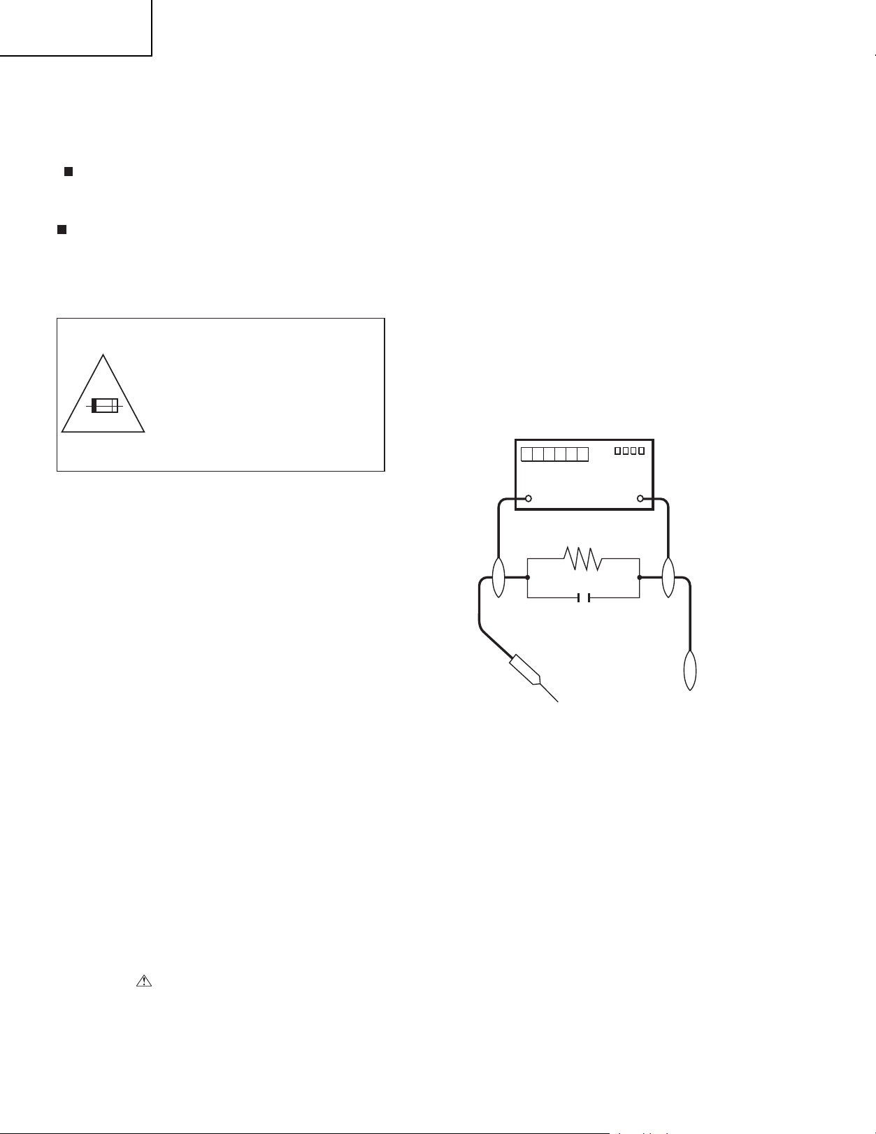
5. To be sure that no shock hazard exists, check for leakage current in
the following manner.
•Plug the AC cord directly into a 120 volt AC outlet.
•Using two clip leads, connect a 1.5k ohm, 10 watt resistor paralleled by a 0.15 F capacitor in series with all exposed metal cabinet
parts and a known earth ground, such as electrical conduit or electrical ground connected to an earth ground.
///////////////////////////////////////////////////////////////////////////////////////////////////////////////////////////////////////////////////////////////////////////////////////////////////////////////////////////////////////////
µ
TO EXPOSED
METAL PARTS
AC SCALE
1.5k ohm
10W
0.15µF
TEST PROBE
CONNECT TO
KNOWN EARTH
GROUND
SAFETY NOTICE
Many electrical and mechanical parts in LCD color television have
special safety-related characteristics.
These characteristics are often not evident from visual inspection, nor
can protection afforded by them be necessarily increased by using
replacement components rated for higher voltage, wattage, etc.
Replacement parts which have these special safety characteristics are
identified in this manual; electrical components having such features
Par
ts
are identified by " " and shaded areas in the Replacement
and Schematic Diagrams.
///////////////////////////////////////////////////////////////////////////////////////////////////////////////////////////////////////////////////////////////////////////////////////////////////////////////////////////////////////////
Lists
For continued protection, replacement parts must be identical to those
used in the original circuit.
The use of a substitute replacement parts which do not have the same
safety characteristics as the factory recommended replacement parts
shown in this service manual, may create shock, fire or other hazards.
2
Page 3
PRECAUTIONS A PRENDRE LORS DE LA REPARATION
s
s
-
Ne peut effectuer la réparation qu' un technicien spécialisé qui s'est parfaitement accoutumé à toute vérification de sécurité et aux
conseils suivants.
Al'aide de deux fils à pinces, brancher une résistance de 1.5 k
AVERTISSEMENT
1.
N'entreprendre Aaucunemodification de tout circuit. C'est dangereux.
2.
Débrancher le récepteur avant toute réparation.
PRECAUTION: POUR LA PROTECTION CONTINUE CONTRE
LES RISQUES D'INCENDIE, REMPLACER LE FUSIBLE
AV
F1(250V 3.15A), F101 (125 5A)
VERIFICATIONS CONTRE L'INCEN-DIE ET LE
CHOC ELECTRIQUE
Avant de rendre le récepteur à l'utilisateur , effectuer les vérifications suivantes.
3.
Inspecter tous les faisceaux de câbles pour s'assurer que les fils
ne soient pas pincés ou qu'un outil ne soit pas placé entre le châssis et les autres pièces métalliques du récepteur.
4.
Inspecter tous les dispositifs de protection comme les boutons de
commande non-métalliques, les isolants, le dos du coffret, les couvercles ou blindages de réglage et de compartiment, les réseaux
de résistancecapacité, les isolateurs mécaniques, etc.
S'assurer qu'il n'y ait pas de danger d'électrocution en vérifiant la
5.
fuite de courant, de la facon suivante:
Brancher le cordon d'alimentation directem-ent à une prise de courant de 120V. (Ne pas utiliser de transformateur d'isolation pour
cet essai).
10 watts en parallèle avec un condensateur de 0.15µFensérie
avec toutes les pièces métalliques exposées du coffret et une terre
connue comme une conduite électrique ou une prise de terre
branchée à la terre.
Utiliser un voltmètre CA d'une sensibilité d'au moins 5000 /V pour
mesurer la chute de tension en travers de la résistance.
Toucher avec la sonde d'essai les pièces métalliques exposées qui
présentent une voie de retour au châssis (antenne, coffret métallique, tête des vis, arbres de commande et des boutons, écusson,
etc.) et mesurer la chute de tension CA en-travers de la résistance.
Toutes les vérifications doivent être refaites après avoir inversé la
fiche du cordon d'alimentation. (Si nécessaire, une prise
d'adpatation non polarisée peut être utilisée dans le but de terminer ces vérifications.)
La tension de pointe mesurèe ne doit pas dépasser 0.75V (correspondante au courant CA de pointe de 0.5mA).
Dans le cas contraire, il y a une possibilité de choc électrique qui
doit être supprimée avant de rendre le récepteur au client.
DVM
ECHELLE CA
1.5k ohm
10W
µ
F
0.15
SONDE D'ESSAI
LC-20D42U
AUX PIECES
METALLIQUES
EXPOSEES
/////////////////////////////////////////////////////////////////////////////////////////////////////////////////////////////////////////////////////////////////////////////////////////////////////////////////////////////////////////////
BRANCHER A UNE
TERRE CONNUE
AVIS POUR LA SECURITE
De nombreuses pièces, électriques et mécaniques, dans les téléviseur ACL présentent des caractéristiques spéciales relatives à la sécurité, qui ne sont souvent pas évidentes à vue. Le degré de protection ne peut pas être nécessairement augmentée en utilisant des
pièces de remplacement étalonnées pour haute tension, puissance,
etc.
Les pièces de remplacement qui présentent ces caractéristiques sont
identifiées dans ce manuel; les pièces électriques qui présentent ces
particularités sont identifiées par la marque " " et hachurées dans la
liste des pièces de remplacement et les diagrammes schématiques.
/////////////////////////////////////////////////////////////////////////////////////////////////////////////////////////////////////////////////////////////////////////////////////////////////////////////////////////////////////////////
Pour assurer la protection, ces pièces doivent être identiques à celle
utilisées dans le circuit d'origine. L'utilisation de pièces qui n'ont pa
les mêmes caractéristiques que les pièces recommandées par l'usine,
indiquées dans ce manuel, peut provoquer des électrocutions, incen
dies, radiations X ou autres accidents.
3
Page 4
LC-20D42U
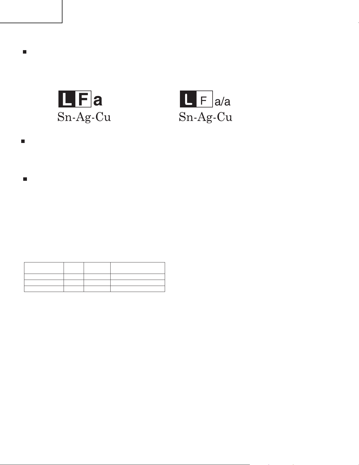
Precautions for using lead-free solder
Employing lead-free solder
•“PWBs” of this model employs lead-free solder. The LF symbol indicates lead-free solder, and is attached on the PWBs and service manuals. The
alphabetical character following LF shows the type of lead-free solder.
Example:
Indicates lead-free solder of tin, silver and copper. Indicates lead-free solder of tin, silver and copper.
Using lead-free wire solder
•When fixing the PWB soldered with the lead-free solder, apply lead-free wire solder. Repairing with conventional lead wire solder may cause damage or accident due to cracks.
As the melting point of lead-free solder (Sn-Ag-Cu) is higher than the lead wire solder by 40
bit, if you are not familiar with how to obtain lead-free wire solder or soldering bit, contact our service station or service branch in your area.
Soldering
•As the melting point of lead-free solder (Sn-Ag-Cu) is about 220
solder wettability, you may be apt to keep the soldering bit in contact with the PWB for extended period of time. However, Since the land may be
peeled off or the maximum heat-resistance temperature of parts may be exceeded, remove the bit from the PWB as soon as you confirm the
steady soldering condition.
Lead-free solder contains more tin, and the end of the soldering bit may be easily corroded. Make sure to turn on and off the power of the bit as
required.
If a different type of solder stays on the tip of the soldering bit, it is alloyed with lead-free solder. Clean the bit after every use of it.
When the tip of the soldering bit is blackened during use, file it with steel wool or fine sandpaper.
°C which is higher than the conventional lead solder by 40 °C, and as it has poor
°C, we recommend you to use a dedicated soldering
•Be careful when replacing parts with polarity indication on the PWB silk.
Lead-free wire solder for servicing
PARTS CODE
ZHNDAi123250E BL J 0.3mm 250g (1roll)
ZHNDAi126500E BK J 0.6mm 500g (1roll)
ZHNDAi12801KE BM J 1.0mm 1kg (1roll)
PRICE
RANK
PART
DELIVERY
DESCRIPTION
φ
φ
φ
4
Page 5
SPECIFICATIONS
LC-20D42U
Item
LCD panel
Number of dots
TV
Function
TV-standard (CCIR)
Receiving
Channel
Audio multiplex
Backlight
Audio out
Terminals
Rear
Front
Side
USB SOFT UPDATE (When service man and products USB is used only by update of program.
OSD language
Power Requirement
Power Consumption
Model
LC-20D42U
20"Advanced Super View & BLACK TFT LCD
×
3,147,264 dots (1366 768 3 dots)
×
American TV Standard ATSC/NTSC System
VHF/UHF
CATV
Digital Terretrial
Broadcast(8VSB)
Digital cable
(64/256 QAM)
VHF 2-13ch, UHF 14-69ch
1-135ch (non-scrambled channel only)
2-69ch
*1
1-135ch (non-scrambled channel only)
BTSC System
60,000 hours (at Backlight Standard position)
×
5W 2
INPUT 1
INPUT 2
INPUT 3
INPUT 4
INPUT 5
AV in, COMPONENT in
AV in
AV in, S-VIDEO in
HDMI in with HDCP
HDMI Analog Audio in, HDMI in with HDCP
INPUT 6 15 pin mini D-sub, PC Audio in (Ø 3.5 mm jack)
ANTENNA
DIGITAL AUDIO OUTPUT
75 Ω Unbalance, F Type 1 for Analog (VHF/UHF/CATV) and Digital (AIR/CABLE)
Optical Digital audio output 1 (PCM/Dolby Digital)
×
×
OUTPUT Audio out
MOBILE AUDIO
Mobile Audio in
The ordinary user never uses it. )
English/French/Spanish
AC 120 V, 60 Hz
69 W (0.3 W Standby with AC 120V)
Weight
w/o stand
with stand
Dimension
(W H D)
*2
×
×
w/o stand
with stand
Operating temperature
*1
Emergency alert messages via Cable are unreceivable.
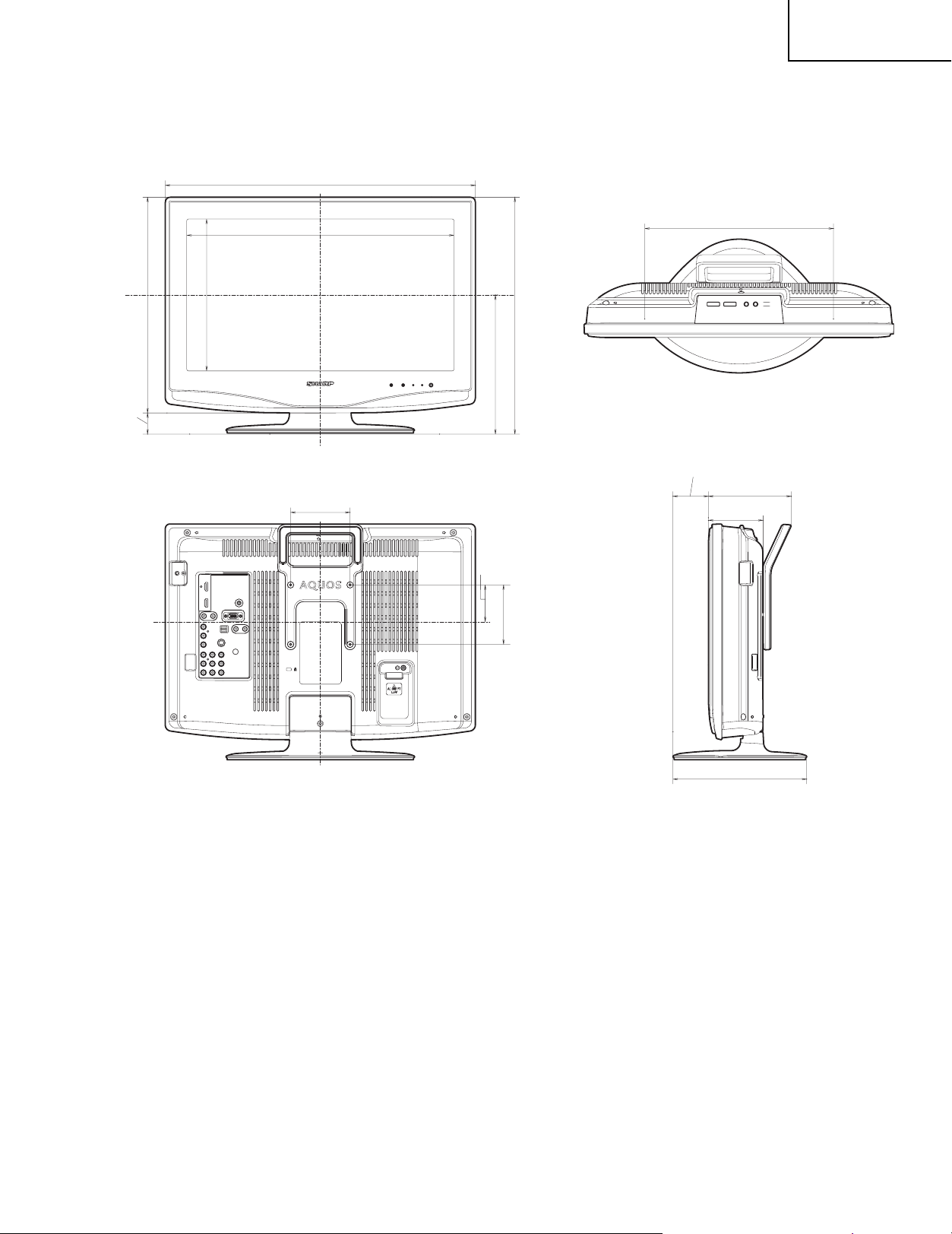
*2
The dimensional drawings are shown on the inside back cover.
As part of policy of continuous improvement, SHARP reserves the right to make design and speci cation changes for product
*
15.8 lbs./12.0 kg
13.2 lbs./14.5 kg
35
20
/64 1545/64 855/64 inch
35
×
/64 1419/64 533/64 inch
20
+
32˚F to 104˚F (0˚C to 40˚C)
×
×
×
+
+
improvement without prior notice. The performance speci cation gures indicated are nominal values of production units.
There may be some deviations from these values in individual units.
5
Page 6
LC-20D42U
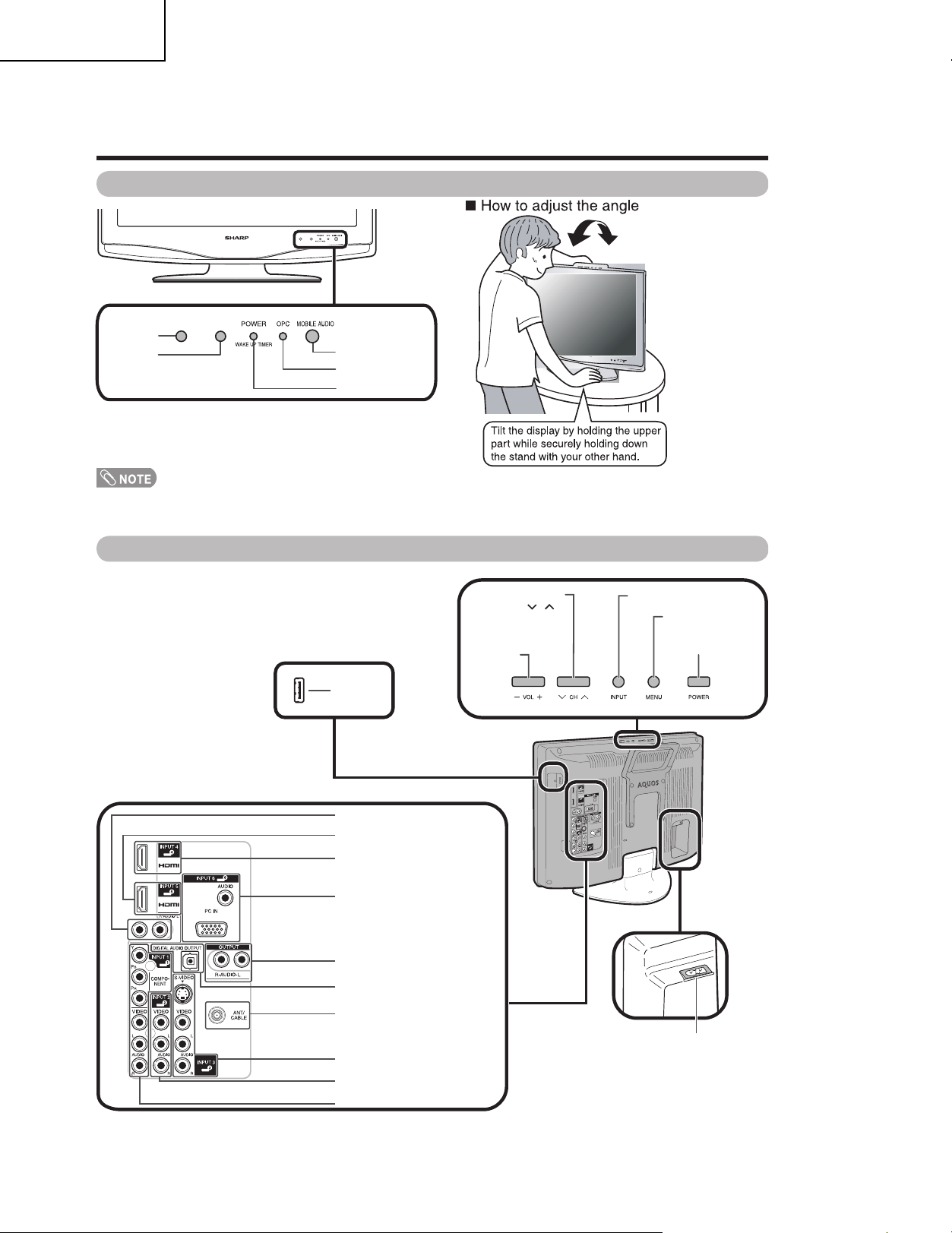
Part names
TV (Front)
Remote
control
sensor
OPC
sensor*
*OPC: Optical Picture Control
**See page 16 for TV status indicator.
TV (Rear)
OPERATION MANUAL
MOBILE
AUDIO jack
OPC indicator*
POWER
indicator**
To change the vertical angle of the LCD TV set,
tilt thescreen up to 2.5 degrees forward or 10
degrees backwards.Please adjust the angle so that
the LCD TV set can be watched most comfortably.
SOFT UPDATE
The ordinary user never
uses it.
USB
terminal
AUDIO terminals (INPUT 5)
HDMI terminal (INPUT 5)
HDMI terminal (INPUT 4)
PC IN terminals (INPUT 6)
AUDIO OUTPUT terminals
DIGITAL AUDIO OUTPUT
terminal
Antenna/Cable in
Channel buttons
(CH / )
Volume
buttons
(VOL + / - )
INPUT button
MENU button
POWER button
INPUT 3 terminals
INPUT 2 terminals
INPUT 1 terminals
AC INPUT terminal
6
Page 7
Part names
LC-20D42U
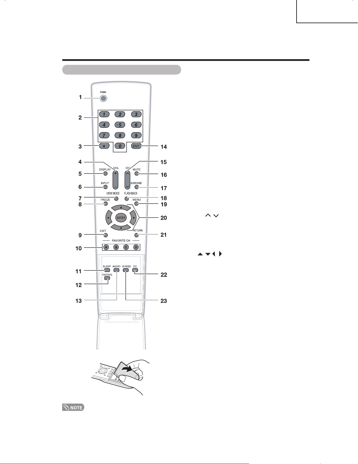
Remote control unit
1 POWER: Switch the TV power on or enters standby.
2 0 - 9: Set the channel.
3 (DOT):
»
+
4 VOL / : Set the volume.
5 DISPLAY: Display the channel and the clock
6 INPUT: Select a TV input source. (TV, INPUT 1,
7 VIEW MODE: Select the screen size.
8 FREEZE: Set the still image. Press again to return to
9 EXIT: Turn off the menu screen.
10 FAVORITE CH
A, B, C, D: Select 4 preset favorite channels in 4
While watching, you can toggle the selected channels
11 SLEEP: Set the sleep timer.
12 FAVORITE: Set the favorite channels.
13 AUDIO: Selects the MTS/SAP or the audio mode
14 ENT: Jumps to a channel after selecting with the 0 - 9
15 CH / : Select the channel.
16 MUTE: Mute the sound.
17 SURROUND: Select Surround settings.
18 FLASHBACK: Return to the previous channel or
external input mode.
MENU: Display the menu screen.
19
20 / / / /ENTER: Select a desired item on the
21 RETURN: Return to the previous menu screen.
22 CC: Display captions from a closed-caption source.
23 AV MODE: Select an audio or video setting.
-
information .
INPUT 2, INPUT 3, INPUT 4, INPUT 5, INPUT 6)
normal screen.
different categories.
by pressing A, B, C and D.
during multi-channel audio broadcasts.
buttons.
screen.
(When the input source is TV, INPUT 1, 2 or 3:
STANDARD, MOVIE, GAME, USER, DYNAMIC (Fixed),
DYNAMIC. When the input source is INPUT 4, 5 or 6:
STANDARD, MOVIE, GAME, PC, USER, DYNAMIC
(Fixed), DYNAMIC)
When using the remote control unit, point it at the TV.
7
Page 8
LC-20D42U
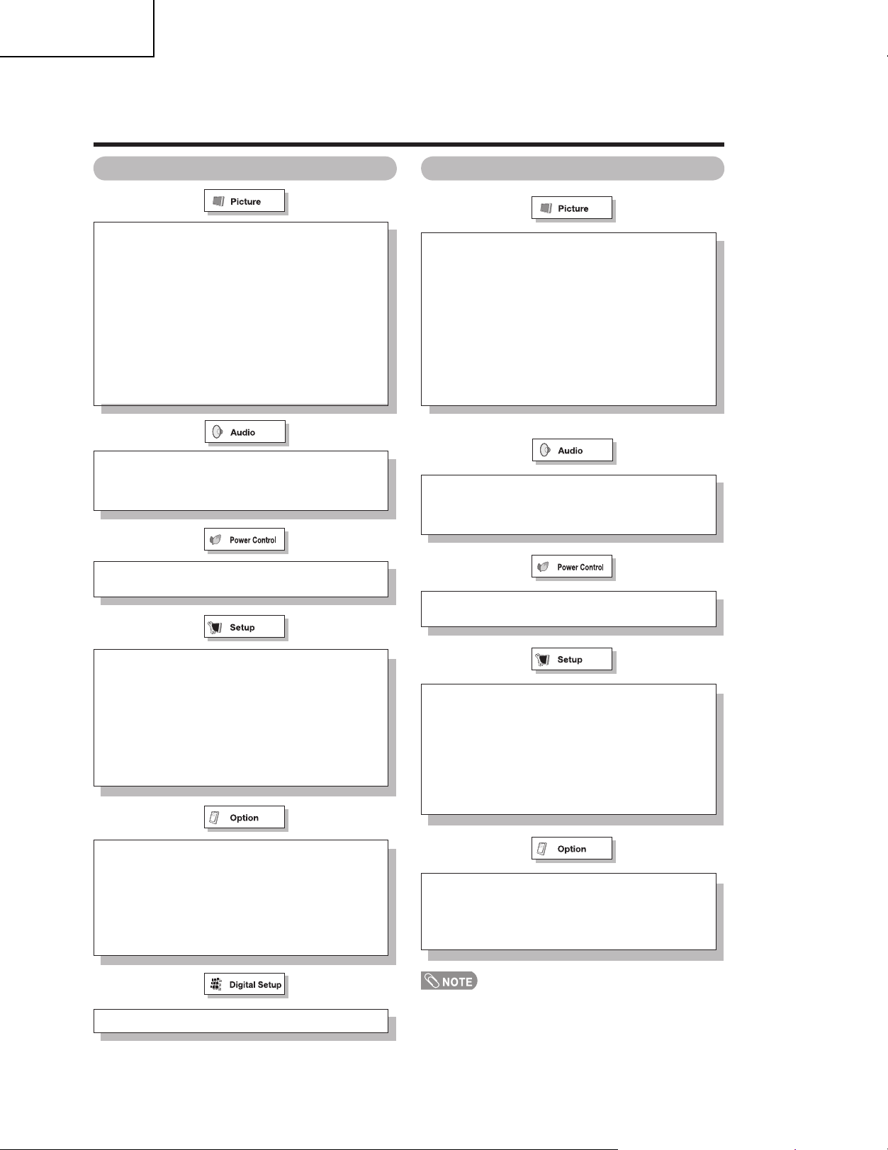
Basic adjustment sitings
Menu items for TV/INPUT 1/2/3 Menu items for HDMI/PC-IN
OPC
Backlight
Contrast
Brightness
Color
Tint
Sharpness
Advanced
Color Temp.
Black
I/P Setting
Film Mode
3D-Y/C
Monochrome
Range of OPC
Treble
Bass
Balance
Surround
No Signal Off
No Operation Off
OPC
Backlight
Contrast
Brightness
Color
Tint
Sharpness
Advanced
Color Temp.
Black
I/P Setting
Film Mode
Monochrome
Range of OPC
Treble
Bass
Balance
Surround
No Signal Off
No Operation Off
EZ Setup
CH Setup
Antenna Setup-DIGITAL
Input Skip
Input Label
Parental CTRL
Position
Language
Clock Setup
Music Player Input
Reset
Audio Only
Digital Noise Reduction
Input Select
Output Select
Color System
Caption Setup
Program Title Display
Favorite CH
Wake-up Timer Setup
Audio Setup
Input Skip
Input Signal
Auto Sync.
Input Label
Fine Sync.
Position
Language
Clock Setup
Music Player Input
Reset
Audio Only
Digital Noise Reduction
HDMI Setup
Output Select
Wake-up Timer Setup
Some menu items may not be displayed depending on the
selected input source.
8
Page 9
17
20
35
15
/32
/64
(522)
(443.6)
DIMENSIONS
12
LC-20D42U
33
/64
(318)
(36)
/64
27
1
(363)
/64
19
14
(249.4)
/16
13
9
(399)
/64
(234)
45
/32
7
15
9
23
2
(60)
/64
33
5
(140)
15
3
/16
(100)
(62)
/16
7
2
(100)
/16
15
3
/64
5
(92)
/8
3
55
(225)
/64
8
9
Page 10
LC-20D42U
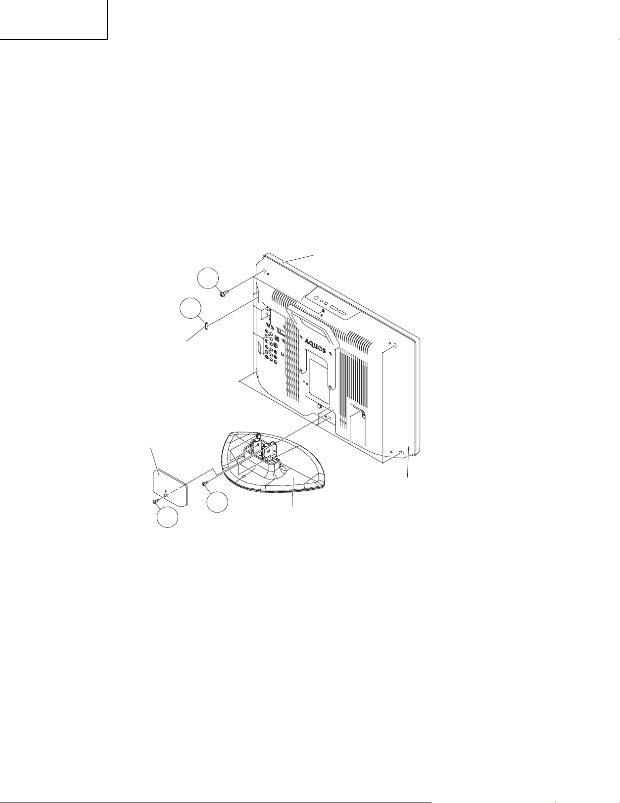
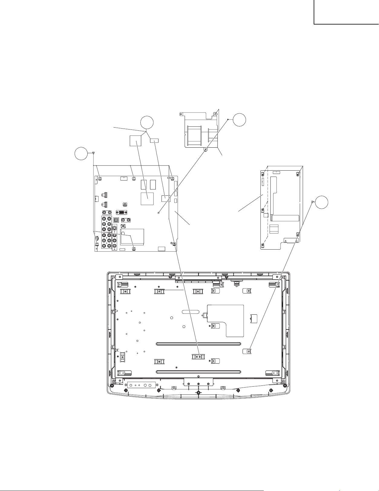
REMOVING OF MAJOR PARTS
1. Remove the lock screw and detach the Stand Cover.
2. Remove the 4 lock screw and detach the Stand Assy.
3. Remove the USB Cover.
4. Remove the 5 lock screws,4 lock screws,3 lock screws,1 lock screw and detach the Cabinet B.
Cabinet A
4
3
USB Cover
Stand Cover
1
Cabinet B
2
Stand Assy
10
Page 11
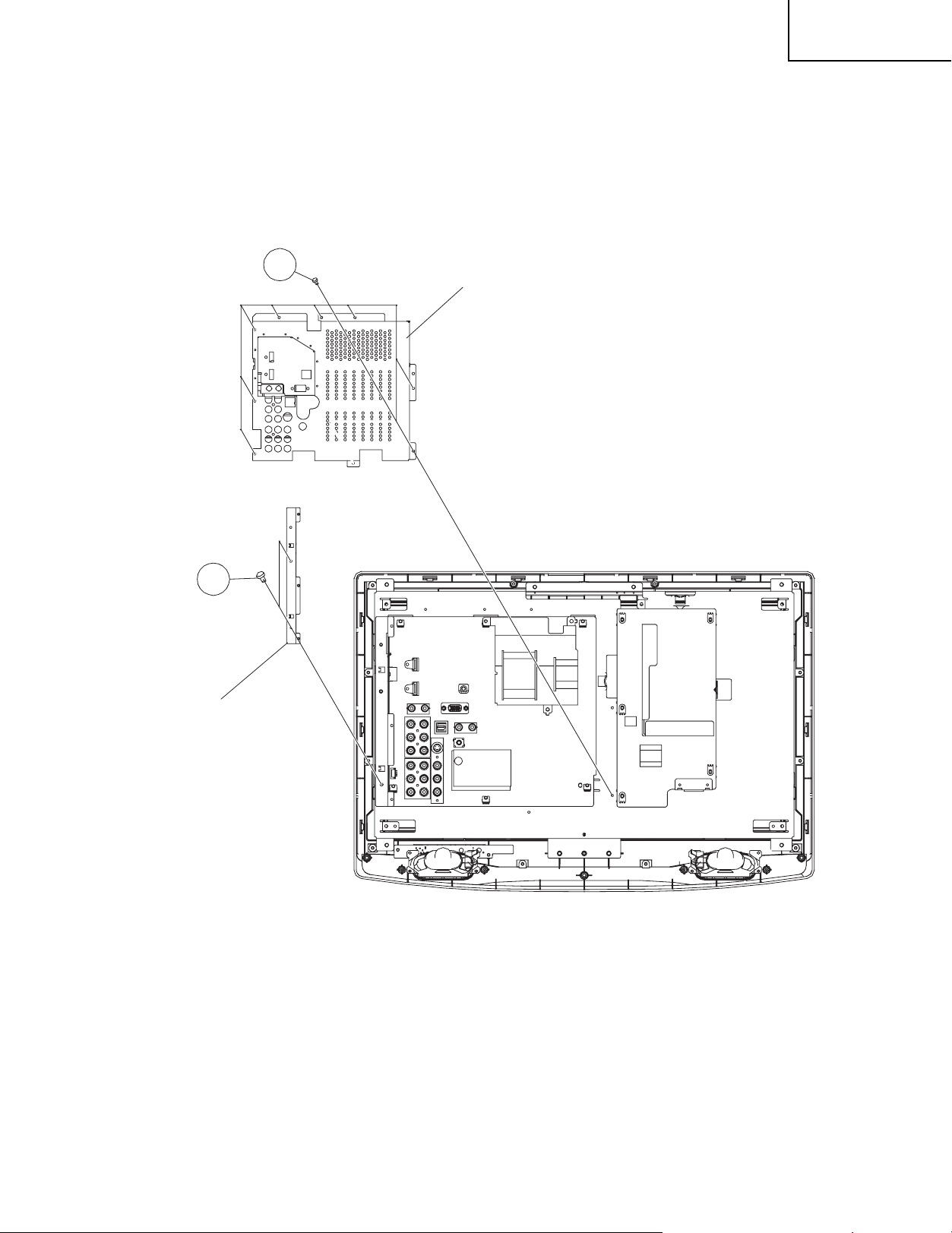
5. Remove the 6 lock screws,3 lock screws and detach the Main Shield.
6. Remove the 2 lock screws and detach the Chassis Frame.
LC-20D42U
6
5
Main Shield
Chassis Frame
11
Page 12
LC-20D42U
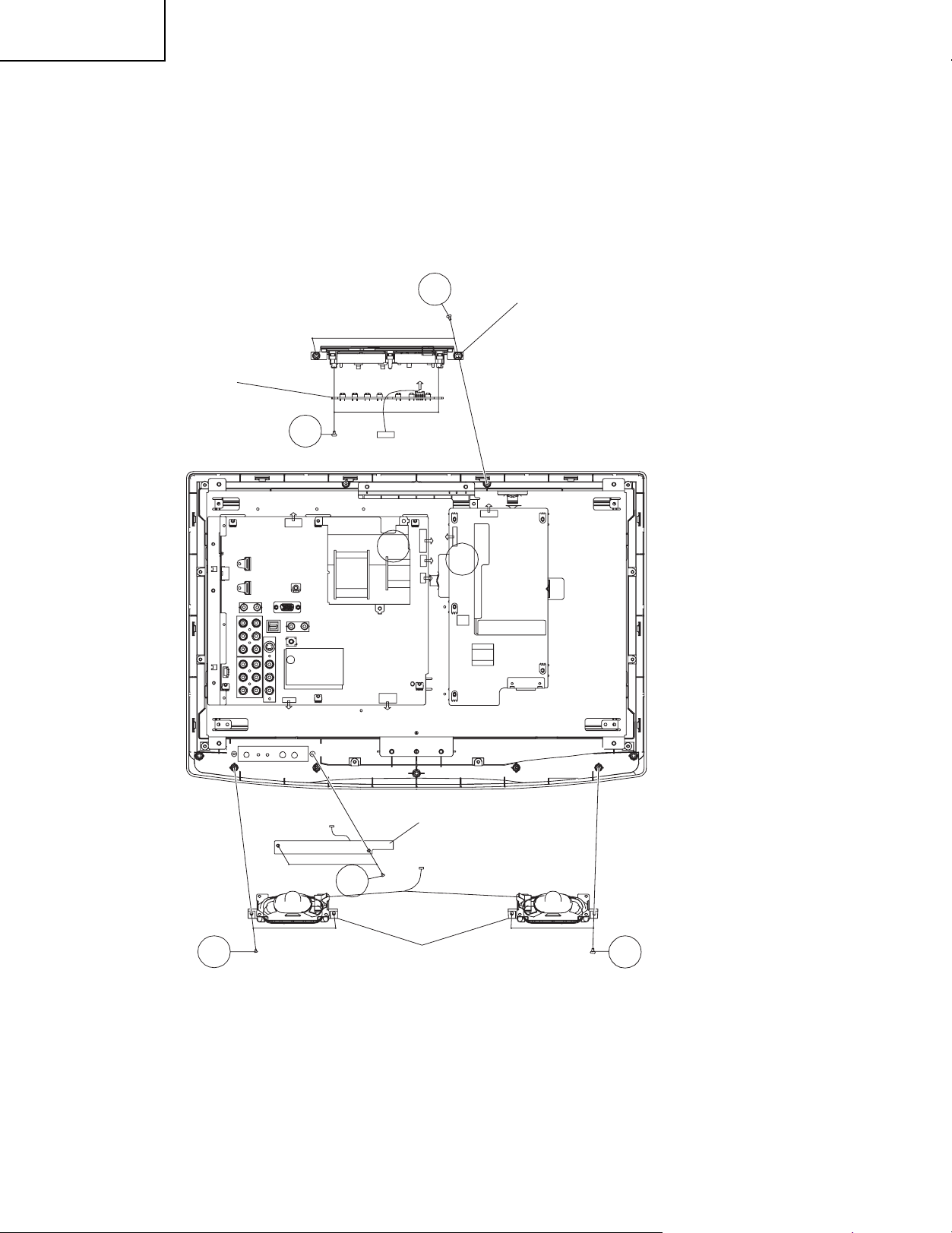
7. Disconnect all the connectors from all he PWBs.
8. Remove the 2 lock screws and detach Top Cover Assy.
9. Remove the 2 lock screws from the Top Cover Assy and detach the KEY Unit.
10.Remove the 4 lock screws and detach the Speaker Assy L&R.
11.Remove the 2 lock screws and detach the R/C LED Unit.
8
Top Cover Assy
KEY Unit
9
10
7
7
R/C LED Unit
11
Speaker Assy L&R
10
12
Page 13
12. Remove the 5 lock screws and detach the POWER Unit.
13. Remove the 6 lock screws and detach the MAIN Unit.
14. Remove the 2 lock rivets and detach the Radiator.
15. Remove the 2 Earth Plate.
LC-20D42U
Earth Plate
13
15
14
Radiator
12
POWER Unit
MAIN Unit
13
Page 14
LC-20D42U
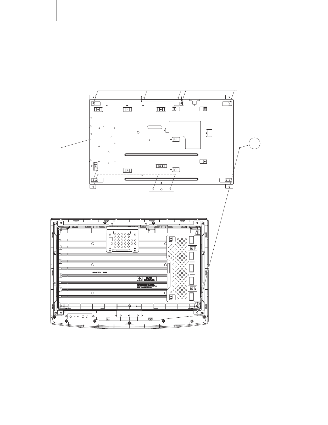
16.Remove the 6 lock screws,5 lock screws and detach the Back Shield.
Back Shield
16
14
Page 15
LC-20D42U
ADJUSTING PROCEDURE OF EACH SECTION
[1] ADJUSTMENT PROCEDURETME
The adjustment values are set to the optimum conditions at the factory before shipping. If a value should become improper or an adjustment is
required due to part replacement,make an adjustment according to the following procedure.
1. After replacement of any PWB unit and/or IC for repair,please note the following.
• When replacing the following units, make sure to prepare the new units loaded with updated software.
MAIN Unit:DUNKE001FMF1
2. Upgrading of each microprocessor software
Caution:Never "POWER OFF" the unit when software upgrade is on going.
Otherwise the system may be damaged beyond recovery.
2.1. Software version upgrade
The model employs the following software.
•
Main software
•Monitor microprocessor software.
The main software and the monitor microprocessor software can be upgraded by using a general-purpose USB Memory.
The followings are the procedures for upgrading,explained separately for each of the main software,the monitor microprocessor software.
2.2. Main software version upgrade
Get ready before you start
• USB Memory of 128MB or higher capacity.
• PC running on Windows 98/98SE/ME/2000/XP operating system.
• USB Memory reader/writer with USB connectivity.
Preparations
To upgrade the main software,it is necessary to get ready the USB Memory for version upgrade before you start.
Follow the steps below and create the USB Memory for version upgrade.
1. Copy the file 42LTAxxx.USB(named temporarily) for version upgrade to the root directory (folder) of the USB Momory.
NOTE:In the USB Memory drive, do not store other folders or unrelated files, or more than one files for version upgrade.
Now the USB Memory for version upgrade is ready.
How to upgrade the software
2.
Unplug the AC cord. (make sure AC power shut down more than 1 minute.)
3. Insert the USB Memory for version upgrade (prepared as above) into the service socket located Right side from center at terminals,above
HDMI4 terminal in the rear of the unit.
4. plug in the AC cord with power button pressing after 5 seconds later, unpress the power button.
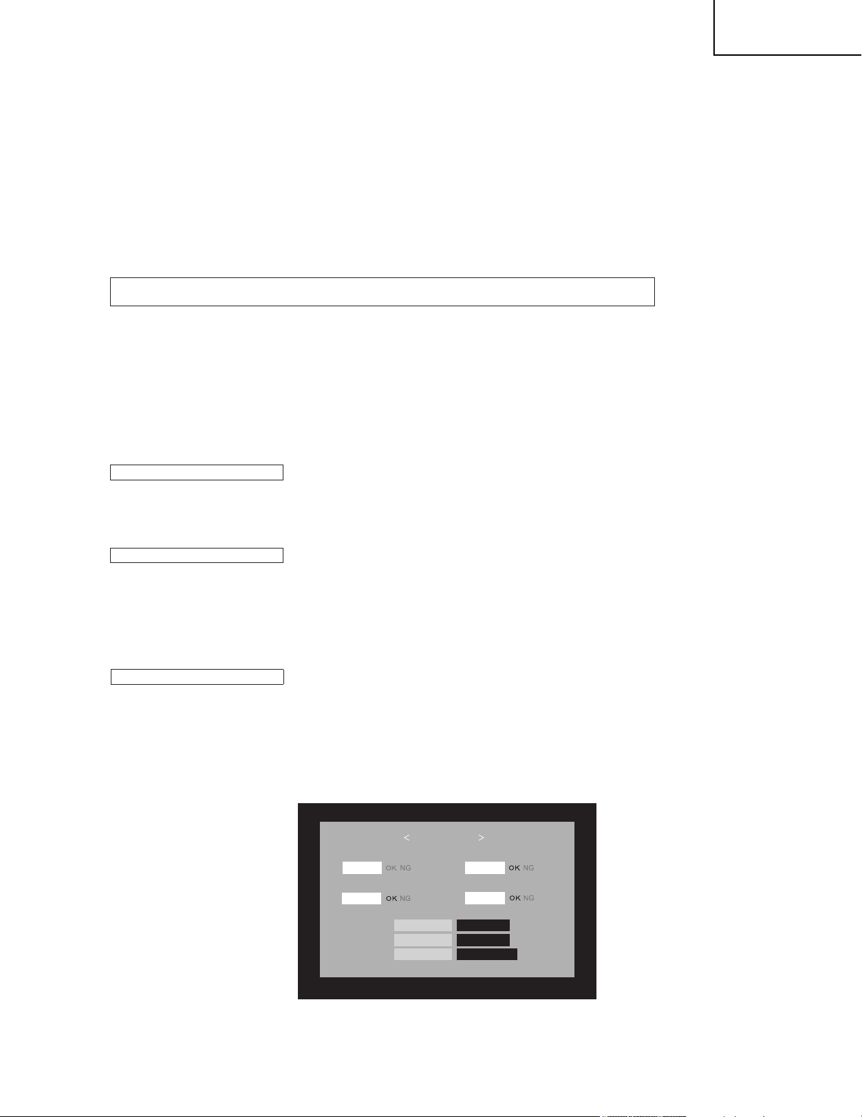
5. After the unit startup,the system upgrade screen as shown below appears within 20-40 seconds.
100%
MOISE_LITE
MAIN
45%
MONITOR
NO DATA
SYSTEM UPGRADE
EEPROM
USB - MEMORY
DETECT
U0612111 OLD Version
NEW Version U0612201
Boot Version
D42U_LITE 0.80
15
Page 16
LC-20D42U
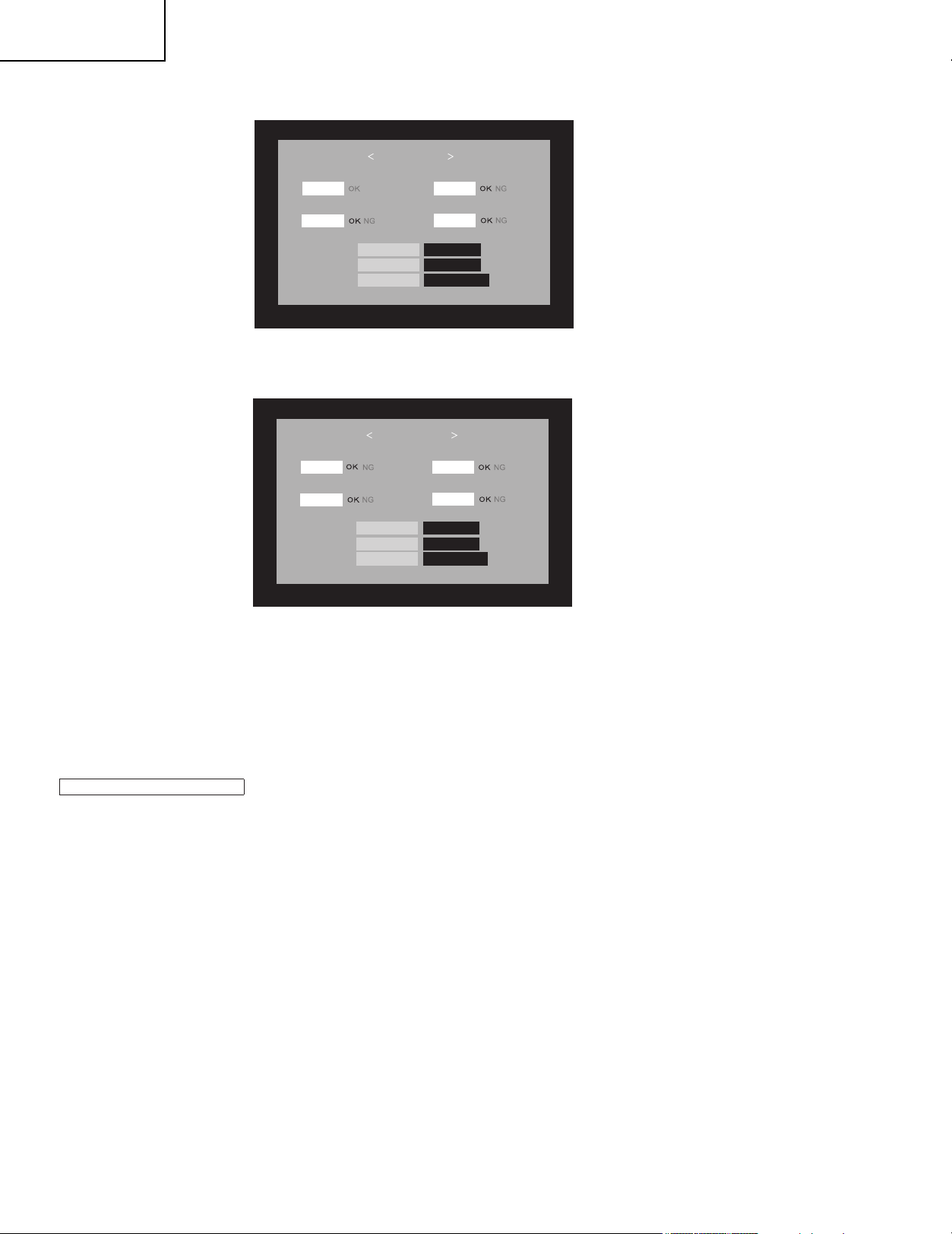
6. Even a single failure in the process will trigger the upgrade failure screen as shown below.the word "NG" channges to red for the item failed.
NOTE: In the event of a failure, repeat the upgrading process.If the process repeatedly fails. it is likely that the hardware is troubled.
100%
100%
MOISE_LITE
MOISE_LITE
SYSTEM UPGRADE
MAIN
45%
MONITOR
NO DATA
NG
NEW Version U0612201
Boot Version
EEPROM
USB - MEMORY
DETECT
U0612111 OLD Version
D42U_LITE 0.80
7.Upon completion of the whole process,the upgrade success screen as shown below appears.You can check the new software version on this
screen. The version information appears after the upgrade is complete.
UPGRADE SUCCESS
MAIN
100%
MONITOR
NO DATA
EEPROM
USB - MEMORY
DETECT
U0612111 OLD Version
NEW Version U0612201
Boot Version
D42U_LITE 0.80
8.unplug the AC cord and remove the USB Memory for version upgrade.
9
.Now the software version upgrade is complete.
NOTE: When you are done with the software version upgrade,start the set,go to the top page of the adjustment process screen and check the main
software version information.
2.3. Monitor microprocessor software version upgrade
Create the USB memory for monitor microprocessor software version upgrade in the same manner as explained in the "Main software version upgrad".
Copy the file 42LTMxxx.USB and 42LTMxxx.BIN(named temorarily ) for monitor microprocessor software version upgrade to th USB memory.
How to upgrade the software
1. Unplug the AC cord.(make sure AC power shut down more than 1 minute.)
2. Insert the USB memory for version upgrade (prepared as above) into the service socket located Right side from center at terminals,above HDMI4
terminal in the rear of the unit.
3. plug in the AC cord with power button pressing.
4. After 5 seconds later,unpress the power botton.
CAUTION: The moment this operation is done,the upgrading of the monitor microprocessor software starts.While the upgrade is ongoing,never power
5. After the upgrade startup, the power light will flash continuous.
off the unit. Otherwise the upgrade will fail and the system may have a serious damage beyond recovery (inability to start).
After the monitor microprocessor software is upgrade, should preform the "Industry Init " by all mean.
16
Page 17
6. A failure in the process will trigger the upgrade failure screen.The word "NG" changes to red for the item failed.
UPGRADE FAILURE
MONITOR
Model err
NG
LC-20D42U
OLD Version
NEW Version
0.95
0.95
NOTE: In the event of a failure,repeat the upgrading process.If the process repeatedly fails, it is likely that the hardware is troubled.
7. Upon completion of the whole process,the set will restart autowatically.
8. Unplug the AC cord and remove the USB Memory for version upgrade.
9. Now the software versin upgrade is complete.
NOTE: When you are done with the software version upgrade,start the set,go to the top page of the adjustment process screen and check the mon-
itor microprocessor software version information and panel size information.
2.4. LCD TV Adjustment item
1.MICON SOFTWARE Writing
(1) Monitor Micon and Main Micon software writing (Main PWB : QPWBXE001WJN1)
Adjustment item
1 Software writing Inspection mode
Adjustment conditions
Connect the tool by using write MAIN soft to P9301 (TL9301,TL9302,TL9310 - TL9355,TL9357,
TL9359,TL9375,TL9378,TL9380 - TL9383) that is mounted on the main PWB,and insert USB
Memory by using MONITOR MICON to main PWB.MONITOR connect to TL8123,TL8124 that
denoted figure. Load stated voltage to MAIN PWB, write the lastest version MAIN SOFT to
file version checking
IC8451, and write the MONITOR MICON SOFT to IC2002, after all completed,turn off the AC
power.
NOTE
When the USB MEMORY cant insert to main PWB or read out is error,MAIN Miro software
must be writed anain.
2. Signal adjustment
(1) Checking the Device
Before starting the adjustment,make sure the adjustment tool and signal generator are set for Sharp LCD US.
Checking the signal generator level adjustment (Set to th standard level)
•
Composite signal : 0.714 Vp-p ± 0.02 (from pedestal to white)
•
15K component signal : Y level : 0.714 Vp-p ± 0.02 (from pedestal to white)
Pb, Pr LEVEL : 0.7 Vp-p ± 0.02 Vp-p
•
33K component signal : Y LEVEL : 0.7 Vp-p ± 0.02 Vp-p (from pedestal to white)
Pb, Pr LEVEL : 0.7 Vp-p ± 0.02 Vp-p
•
Analog RGB signal : RGB LEVEL : from pedestal to white)
0.7 Vp-p ± 0.02 Vp-p
Adjustment procedure
17
Page 18
LC-20D42U
(2).Process mode
Adjustment item Adjustment procedure
Process mode Enter the process adjustment mode using the process adjustment remote controller
1
(3
)Composite N358 signal/tuner adjustment
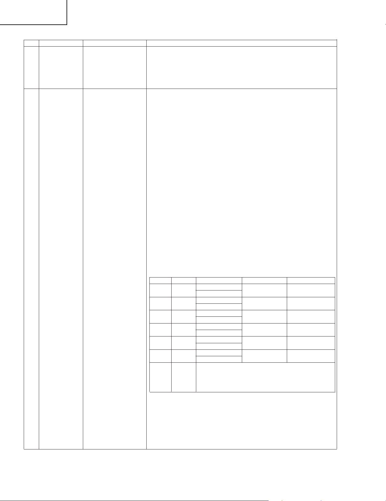
Adjustment item
1 Setting N358 signal
Adjustment conditions
Adjustment conditions
US-10ch
Adjustment procedure
•
Feed the N358 color bar signal(75%)to VIDEO 1 Input
•
Feed the RF signal (by use of US-10CH) to TUNER.
[Video input signal] [US-10ch]
75% Color saturation
100% white 0% black 100% white
2 Automatic adjust-
ment execution
(4) 15K COMPONENT signal adjustment
Adjustment item
1 Setting 480i signal Feed the 100% color Bar signal to VIDEO1 COMPONENT input
2 Automatic adjust-
ment execution
(5) Component 33Ksignal adjustment
Adjustment item
1 Setting 1080i signal Feed the 100% color Bar signal to VIDEO1 CIMPONENT input
Adjustment conditions
Adjustment conditions
Move the cursor to [ N358 ADJ] and press the [ENTER] key.
When [ N358 ADJ OK] appears,the adjustment is complete.
Adjustment procedure
100% Color saturation
100% white
Move the cursor t0 [ COMP 15K ALL ADJ] and press the [ENTER] key..
When [ COMP 15K ALL ADJ OK] appears, the adjustment is complete.
Adjustment procedure
480i
100% color bar
0% black
2 Automatic adjust-
ment execution
100% Color saturation
100% white
Move the cursor to [ HDTV ADJ ] and press the [ENTER] key.
When [ HDTV ADJ OK] appears, the adjustment is complete.
1080i
100% color bar
0% black
18
Page 19
(6) Analog RGB signal adjustment
Adjustment item
1 Setting Analog RGB signal: XGA
Adjustment conditions
(1024x768) 60HZ
SYNC: HV separate
LC-20D42U
Adjustment procedure
Feed the XGA100% color bar signal to analog RGB input.
2Automatic adjust-
ment execution
) Tuner/V-Chip test
(7
Adjustment item
1 Setting NTSC RF signal
2 Automatic adjust-
ment execution
Adjustment conditions
US-4(AIR)ch
100% Color saturation
100% white
Move the cursor to [ ANALOG RGB ADJ] and press the [ENTER] key.
When [ ANALOG RGB ADJ OK] appears ,the adjustment is complete.
•
Feed the NTSC signal to RF ANTENNA.
Move the cursor to[ TUNER VCHIIP TEST(*04ch)] and press the [ENTER] key.
(* Select the channel according to RF signal.)
When [ A-OK(***.**)/VM-OK] appears in blue, the test is complete.(If [A-NG/VM-NG]
appears in yellow or red, the test is incomplete.
Make sure a displacement of ±
Adjustment procedure
0.0625MHZ from the center frequency is acceptable.
XGA
100% color bar
0% black
19
Page 20
LC-20D42U
3.White balance adjustment
Adjustment item
1 Setting For detailed adjustment procedure refer to "Kameyama Model Integral WB Adjustment
2 Automatic adjust-
ment execution
Adjustment conditions
[Command]
Process mode
KRSW0001
KKT10037
Setting
KYOF0000
OSDS0001
SBSL0016
Multi-point adjustment
MSET0001
Adjustment value
initialization
MSET0004
Point 6
WBI60928
MG6G****
MG6B****
MG6R****
Point 5
WBI50800
MG5G****
MG5B****
MG5R****
Point 4
WBI40680
MG4G****
MG4B****
MG4R****
Point 3
WBI30480
MG3G****
MG3B****
MG3R****
Point 2
WBI20312
MG2G****
MG2B****
MG2R****
Point 1
WBI10168
MG1G****
MG1B****
MG1R****
Specifications V1.4".
1) Make the following settings for the set.
2) Connect the white balance adjustment tool to the set.
[Adjustment prcedure]
1) Using the remote controller,transmit the "monitor adjustment process" code.
2) Set the 6
3) Set the 5
4)
5)
6)
7)
8) With the MSET0003 command, write the adjustment values and turn off the AC
* Initial R, G and B settings at point 6: Gradation level set at 928
* Initial R and B settings at points 1 thru 5:Correct the setting same remainder of
RGB setting at each point (This is because the adjustment is made to achieve the
same remainder of RGB setting/4 at each point.
[Adjustment value]
As per the "standard set" submitted by Engineering Department
[LC-20D42U] Teaching Set.
[Adjustment reference] Instrument:[Minolta CA-210] Engineering instrument
Point 6 928 X=0.272 ±0.0012 ±0.0020
Point 5 800 X=0.272 ±0.0012 ±0.0020
Point 4 680 X=0.272 ±0.0012 ±0.0020
Point 3 480 X=0.272 ±0.0012 ±0.0020
Point 2 312 X=0.272 ±0.0020 ±0.0030
Point 1 168 X=0.272 ±0.0035 ±0.0045
Note Set conditions for inspection
AV MODE: [DYNAMIC]
Backlight: +16
Aging time: Min. 60 minutes
th
turn down the R,G and B settings to their reference levels.
Correct the G setting (800 x 6th point G setting /928) (rounded off), and make the R
and B settings to their reference levels.
Set the 4
Correct the G setting (680 x 6th point G setting /928) (rounded off), and make the R
and B settings to their reference levels.
Set the 3rd point to the specified gradation level.
Correct the G setting (480 x 6th point G setting /928) (rounded off), and make the R
and B settings to their reference levels.
Set the 2nd point to the specified gradation level.
Correct the G setting (312 x 6th point G setting /928) (rounded off), and make the R
and B settings to their reference levels.
Set the 1st point to the specified gradation level.
Correct the G setting (168 x 6th point G setting /928) (rounded off), and make the R
and B settings to their reference levels.
power.
point to the specified gradation level,With the strongest color being fixed, ,
th
point to the specified gradation level.
th
point to the specified gradation level.
Level Reference Adj. spec Ins. spec
Adjustment procedure
y=0.277
y=0.2777
y=0.277
y=0.277
y=0.277
y=0.277
AV MODE: [DYNAMIC] (Reset)
Monochro: ON
Aging Time: Min. 60 minutes
Writing
MSET0003
20
Page 21
4. Key writing
1. EDID writing (Main PWB :QPWBXE001WJZZ,Analog RGB/GDMI input terminal)
Adjustment item
1 Analog RGB
EDID writing
HDMI EDID
2
Writing
Adjustment conditions
File Version checking 1) Using the checker,write the EDID data for HDMI to
IC1505 that is mounted on the main PWB.
TL1514: I2C CLODK, TL1515: 12C DATA
TL1516: 5V, TL1517: GND
TL1524: write protection (H:write enable,Low: write
protection)
2) In the analog RGB inspection,use a DDC-compatible
device. If the EDID has been written,the RGB input
does not function normally.
Inspection mode
File version checking
1)
Using the checker,write the analog HDMI EDID data to
IC1501 and IC1502 that are mounted on the main PWB.
TL15108/1510: I2C CLODK, TL1509/1511: 12C DATA
TL1512/1513: 5V, TL1519/1518: GND
TL1534/1535: write protection (H:WP,Low: write enable)
2) Write the data before the HDMI inspection with the
checker.
In the HDMI inspection, use a DDC-compatible device.If
the EDID has been written,the HDMI input does not
function normally.
LC-20D42U
Adjustment procedure
21
Page 22
LC-20D42U
Repeat until RGB
become the target
values.
PC Set
Set the light level to MAX with the light control command
(SBSL0016 for 45).
SBSL0016
Setting is complete.
OK
Multi point adjustment mode setting
MSET0001
Multi point adjustment mode is set.
OK
Initialize adjustment values.
MSET0004
Initialization is done.
OK
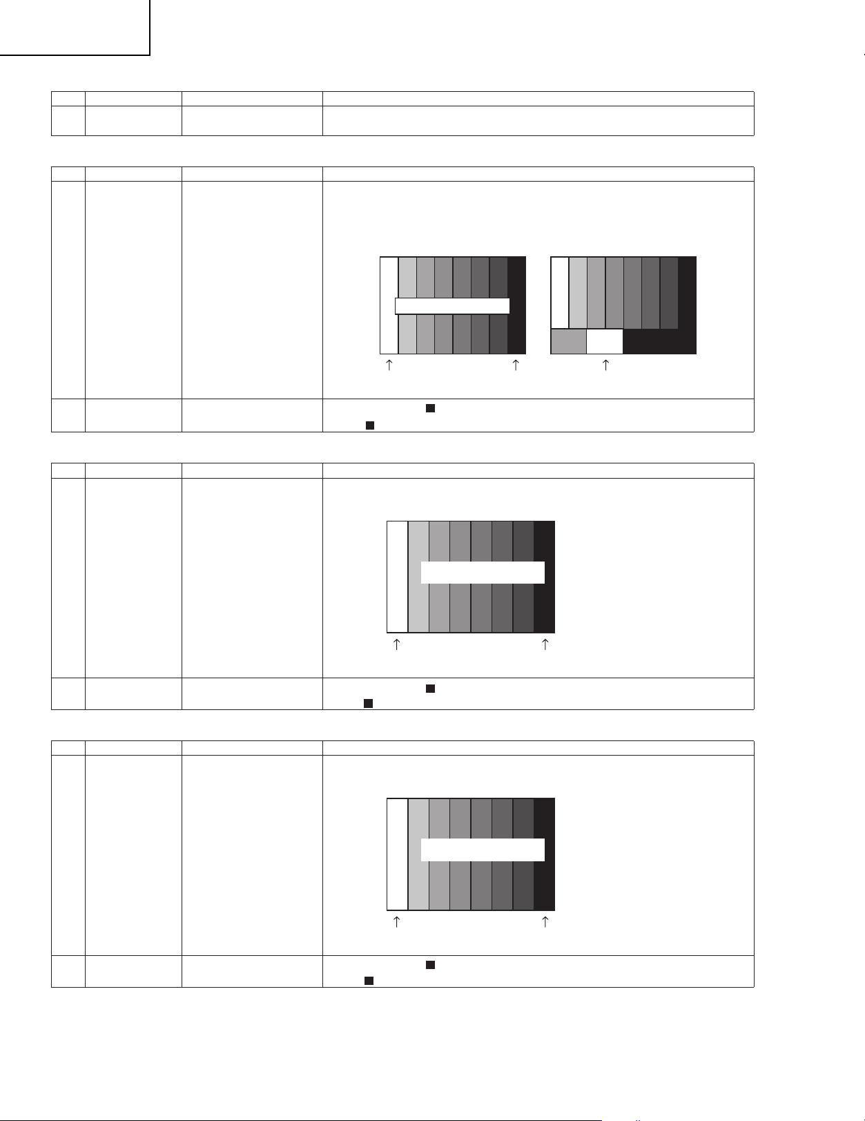
Adjustment gradation setting (point 6 = 232 gradation adjustment*)
LEV60232
Pattern display
Adjustment values are set.
OK
Adjust RGB to the target xy values.
MG6RXXXX
MG6GXXXX
MG6BXXXX
* XXXX indicates the adjusted values between 0000 and 1023
(4 digit decimal number with zero fill).
* In order to adjust by reducing the value, set the strongest color
as the fixed color.
* The default adjustment value of RGB is the parameter value of
the LEV6 command multiplied by 2.
The adjustment value is
reflected in the image.
Adjustment values are set.
OK
Adjustment gradation setting (point 5 = 200 gradation adjustment*)
LEV50200
Pattern display
Adjustment values are set.
OK
Correction of G value
MG5G0800
When G is changed at gradation 6, calculate the ratio of the
change and set the following value to XXXX: (the value set with
LEV5) x 2 x (the ratio).
Adjustment values are set.
OK
22
Page 23
Start measurement
Repeat until RGB
become the target
values.
LC-20D42U
PC Set
Adjust RB to the target xy values.
MG5RXXXX
MG5BXXXX
* XXXX indicates the adjusted values between 0000 and 1023
(4 digit decimal number with zero fill).
* G is fixed.
* The default adjustment value of RGB is the parameter value
of the LEV5 command multiplied by 2.
The adjustment value is
reflected in the image.
Adjustment values are set.
OK
Adjustment gradation setting (point 4 = 170 gradation adjustment*)
LEV40170
Pattern display
Adjustment values are set.
OK
Correction of G value
MG4G0680
When G is changed at gradation 6, calculate the ratio of the
change and set the following value to XXXX: (the value set with
LEV4) x 2 x (the ratio).
Start measurement
Repeat until RGB
become the target
values.
Adjustment values are set.
OK
Adjust RB to the target xy values.
MG4RXXXX
MG4BXXXX
* XXXX indicates the adjusted values between 0000 and 1023
(4 digit decimal number with zero fill).
* G is fixed.
* The default adjustment value of RGB is the parameter value of
the LEV4 command multiplied by 2.
The adjustment value is
reflected in the image.
Adjustment values are set.
OK
Adjustment gradation setting (point 3 = 120 gradation adjustment*)
LEV30120
Pattern display
Adjustment values are set.
OK
Correction of G value
MG3G0480
When G is changed at gradation 6, calculate the ratio of the
change and set the following value to XXXX: (the value set with
LEV3) x 2 x (the ratio).
Adjustment values are set.
OK
23
Page 24
LC-20D42U
Start measurement
Repeat until RGB
become the target
values.
PC Set
Adjust RB to the target xy values.
MG3RXXXX
MG3BXXXX
* XXXX indicates the adjusted values between 0000 and 1023
(4 digit decimal number with zero fill).
* G is fixed.
* The default adjustment value of RGB is the parameter value of
the LEV3 command multiplied by 2.
The adjustment value is
reflected in the image.
Adjustment values are set.
OK
Adjustment gradation setting (point 2 = 78 gradation adjustment*)
LEV20078
Pattern display
Adjustment values are set.
OK
Correction of G value
MG2G0312
When G is changed at gradation 6, calculate the ratio of the
change and set the following value to XXXX: (the value set with
LEV2) x 2 x (the ratio).
Start measurement
Repeat until RGB
become the target
values.
Adjustment values are set.
OK
Adjust RB to the target xy values.
MG2RXXXX
MG2BXXXX
* XXXX indicates the adjusted values between 0000 and 1023
(4 digit decimal number with zero fill).
* G is fixed.
* The default adjustment value of RGB is the parameter value of
the LEV2 command multiplied by 2.
The adjustment value is
reflected in the image.
Adjustment values are set.
OK
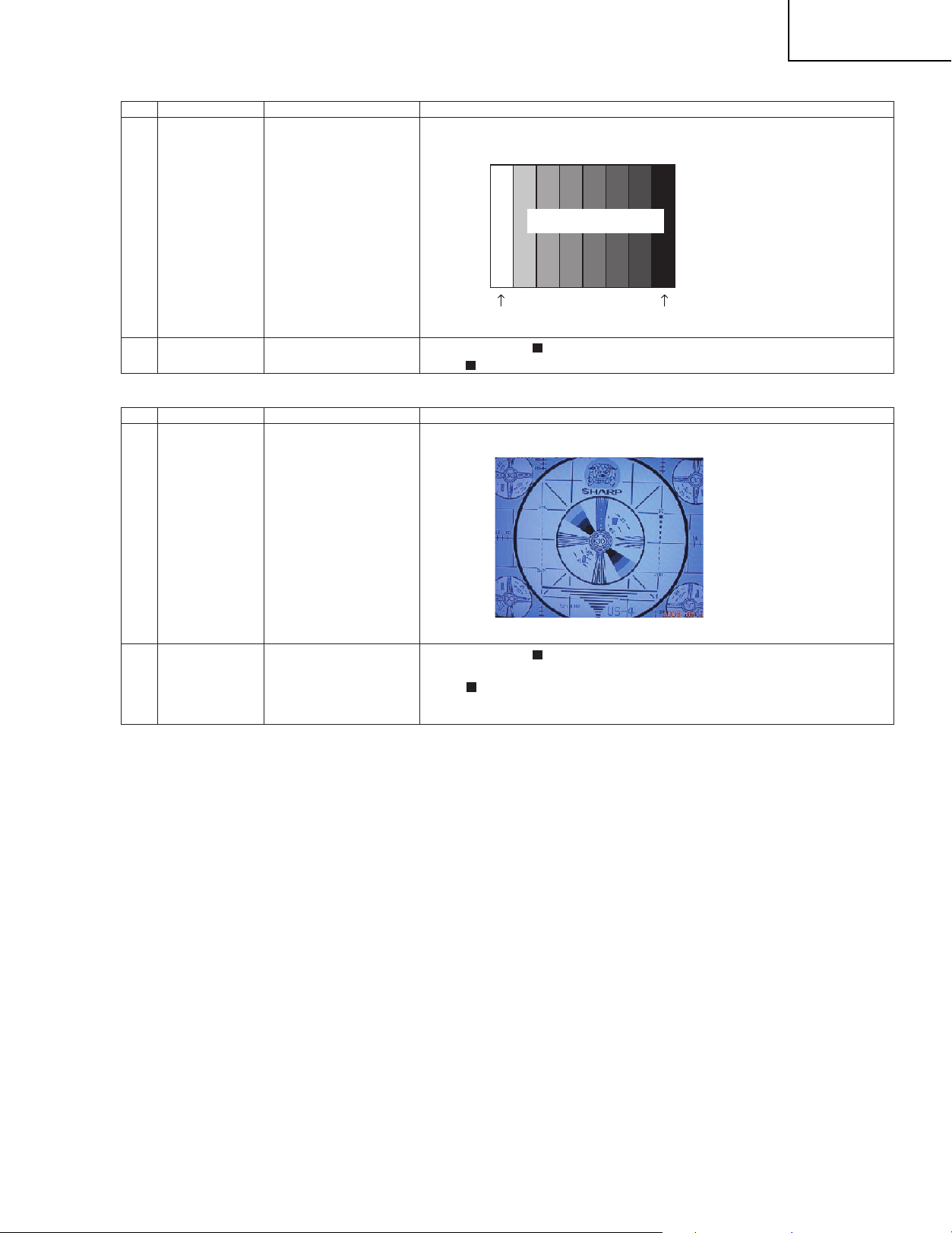
Adjustment gradation setting (point 1 = 42 gradation adjustment*)
LEV10042
Pattern display
Adjustment values are set.
OK
Correction of G value
MG1G0168
When G is changed at gradation 6, calculate the ratio of the
change and set the following value to XXXX: (the value set with
LEV1) x 2 x (the ratio).
24
Adjustment values are set.
OK
Page 25
g
Start measurement
Repeat until RGB
become the target
values.
LC-20D42U
PC Set
Adjust RB to the target xy values.
MG1RXXXX
MG1BXXXX
*XXXX indicates the adjusted values between 0000 and 1023
(4 digit decimal number with zero fill).
* G is Fixed.
* The default adjustment value of RGB is the parameter value of
the LEV1 command multiplied by 2.
The adjustment value is
reflected in the image.
Adjustment values are set.
OK
Writing of adjusted values
MSET0003
Writing is complete.
OK
Deleting adjustment patterns
MSET0000
Deletion is complete.
OK
Completion of adjustment
5. Factory settings
After making the factory settings.pull off the AC cord.
NOTE: Do not turn on the power once the factory settings have been made. Otherwise the factory setting must be made again.
Adjustment item
1 Factory settings Finally pull off the AC cord. • Move the cursor to the [INDUSTRY INIT] line. Using the
Adjustment conditions
[VOL+/-] keys. set this item ON and press the [ENT] key.
The version confirm window appears on the green
screen. When [SUCCESS] appears at the top, the factory settings are complete.(If an error occurs.[ERROR]
appears on the red screen.)
• Finally turn off AC power.
The following settings are returned to the factory ones.
1) User settings
2) Channel data (broadcast frequencies,etc.)
3) Password setting
4) Operation time
5) Automatic installation flag
6) V-CHIP block setting
Adjustment procedure
6. Software version
The software version will be reported at the Conversion Judgment Meeting. Possible modifications that will follow will be reported using the Modifications Report.
* Main microprocessor
* Monitor microprocessor
* EDID data (HDMI/analo
RGB)
25
Page 26
LC-20D42U
PUBLIC MODE SETTING PROCEDURE
1. How to start Public Mode
• There are the following two ways to get the public mode setup screen displayed.
1 In the adjustment process mode, turn on "HOTEL MODE". Also press the "CH (ù)" and "VOL (+)" keys on
the set at once and turn on the power.
2 1) Press the "INPUT" and "VOL (+)" keys on the set at once and turn on the power.
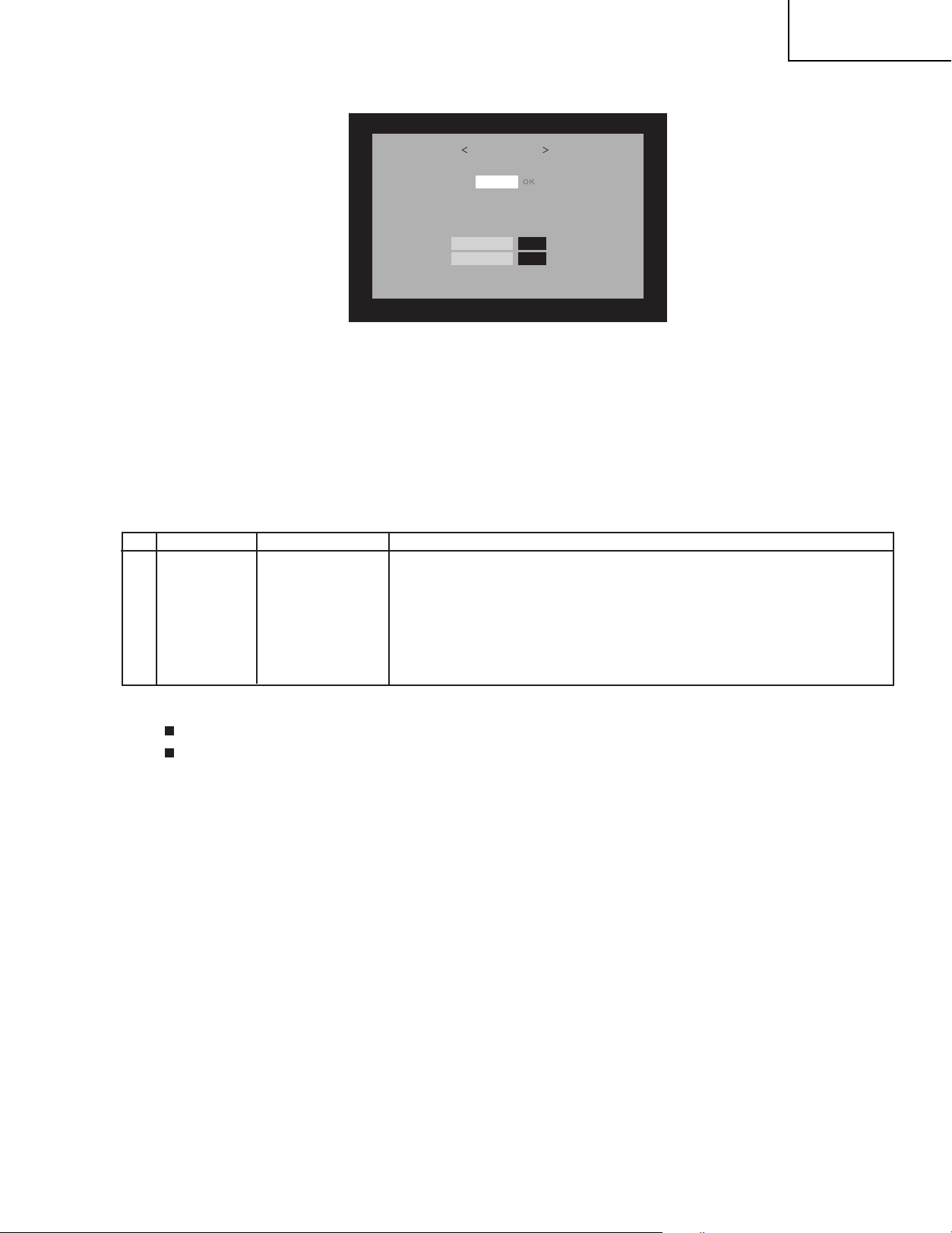
2) Get the password input screen displayed.
Procedure
• The input starts with the leftmost digit.
• Use the numeric keys [1] thru [9] and [0] key on the remote controller.
The other keys are not acceptable.
• With a numeric-key input, "–" will change to " ". The input position
will move one digit to the right.
• With all the 3 digits entered, the password will be verified.
3) The 3-digit password is now verified.
The password [0] [2] [7] provides for the public mode screen. (This screen comes on with whatever
adjustment process settings.)
With any other passwords, the screen changes to the normal mode.
26
Page 27

LC-20D42U
2. How to exit Public Mode
There are the following ways to quit the public mode setup screen.
• Tu rn off "HOTEL MODE" in the adjustment process mode. (✩) ← This way alone is not for quitting the setup
screen, but for quitting the mode itself.
• Tu rn off the power with the "POWER" key. (★)
• Select "EXECUTE". (★)
★ ... "HOTEL MODE" stays on in the adjustment process mode.
✩ ... The settings will be back to the factory ones.
3. Public Mode Setting Values
• With the factory settings made, the public mode settings get initialized. (The adjustment process remains intact.)
4. Public Mode Menu
The guidance is not displayed onscreen.
Setup procedure
• To move the cursor up and down, use the "cursor UP/DOWN" key (remote controller) and "CH (ù)/(Ù)" key
(remote controller and set).
• To change the settings, use the "cursor RIGHT/LEFT" key (remote controller) and "VOL (+)/(–)" key (remote
controller and set).
• To save new settings, keep the cursor at "EXECUTE" and use the "ENTER" key (remote controller) .
Public mode
Power on fixed [Variable ]
Maximum volume [ 60 ]
Volume fixed [Variable ]
Volume fixed level [ 60 ]
RC button [Respond ]
Panel button [Respond ]
Menu button [Respond ]
On screen display [Yes ]
Input mode start [Normal ]
Input mode fixed [Variable ]
Reset
EXECUTE
27
Page 28
LC-20D42U
5. On Setting Items
* "EZ-SETUP" discussed below indicates "EZ-SETUP after the first power-on".
(1) POWER ON FIXED
Selection
Default
Explanation
Limit in Setting
Exception
Remarks
(2) MAXIMUM VOLUME
Selection
Default
Explanation
Limit in Setting
Exception
Remarks
Selection between
"Var iable" and "Fixed" (loop provided)
Variable
In
"Fixed" setting, the power-off by the power key of the unit is invalidated and the image is kept being
received. The power can be turned off by stopping the power supply from AC.
Refer to the
"Power-On Fixed" sheet.
None
Adjustment from 0 to 60 (no loop)
60
Sound volume can not be adjusted higher than the preset value.
•
When the sound volume is set lower than 59, only figures are displayed and the sound volume bar is not
displayed.
•
The maximum sound volume for ON-timer (Wake up timer) is limited also to the preset value.
None
•
In line output (sound volume variable), the sound volume can be adjusted from 0 to 60 irrespective of preadjusted value.
•
When the sound volume is set higher than the MAX setting by the adjusting process, the sound volume
control operation is prohibited for turn-up and the sound volume should be turned down to MAX in this
state.
(3) VOLUME FIXED
Selection
Default
Explanation
Limit in Setting
Exception
Remarks
Selection between "Variable" and "Fixed" (loop provided)
Variable
Sound volume is fixed and made invariable.
•
•
None
•
•
•
The sound volume for the ON-timer (Wake up timer) is fixed also without display of menu. Besides, the
setting is made impossible. (Basically, the menu is not displayed.)
The following keys become invalid:
•
Sound volume Up/Down (VOL +/-) [for both remote control and the unit]
•
Mute (MUTE)
In line output (sound volume variable), the sound volume can be adjusted from 0 to 60 irrespective of preadjusted value.
As for sound volume fixing and sound volume MAX level, the sound volume fixing has priority.
Once the sound volume has been changed by adjustment process, it should be set back to the sound
volume preset by sound volume fixing level when the adjustment process ends .
28
Page 29
(4) VOLUME FIXED LEVEL
Selection
Default
Explanation
Limit in Setting
Exception
Remarks
Adjustment from 1 to 60 (no loop)
60
The sound volume to be fixed by
None
None
Setting is valid only when
(5) R/C BUTTON
Selection
Default
Explanation
Limit in Setting
Exception
Remarks
Selection between
Respond
Keys acceptable by remote control are limited or reception of keys can be prohibited.
In
"No respond" setting, all the keys (including the power key) are not accepted.
•
Adjustment process, factory setting, inspection process and hotel only keys are valid irrespective of setting.
•
All the keys can be used in adjustment process, inspection mode and hotel menu irrespective of setting.
•
All the keys can be used also in the initial EZ-Setup after power-ON irrespective of setting.
(6) PANEL BUTTON
Selection
Default
Explanation
Limit in Setting
Exception
Remarks
Selection between
Respond
All the operations by keys (except the power key) of the unit can be invalidated.
•
Inspection mode and hotel menu mode can be started irrespective of setting.
•
All the keys can be used in adjustment process, inspection mode and hotel menu irrespective of setting.
•
In U.S.A model, all the keys can be used also in the initial EZ-Setup after power-ON irrespective of
setting.
LC-20D42U
"Volume fixed" is determined.
"Volume fixed" is selected for "fixed".
"Respond" and "No respond" (loop provide)
"Respond" and "No respond" (loop provide)
(7) MENU BUTTON
Selection
Default
Explanation
Limit in Setting
Exception
Remarks
Selection between "Respond" and "No respond" (loop provide)
Respond
In
unit are invalidated.
•
•
•
"No respond" setting, the menu operation by the menu key of the remote control and the menu key of the
Inspection mode and hotel menu mode can be started irrespective of setting.
All the keys can be used in adjustment process, inspection mode and hotel menu irrespective of setting.
All the keys can be used also in the initial EZ-Setup after power-ON irrespective of setting.
29
Page 30
LC-20D42U
(8) ON SCREEN DISPLAY
Selection
Default
Explanation
Limit in Setting
Others
Exception
Remarks
Selection between "Ye s " , "NO" (loop provide)
Ye s
The following OSD displays are made ineffective.
Displays of menu group, channel call, sound volume bar and direct key call
•
ON-timer (Wake-up timer) is cleared and set to "OFF".
•
Set time of the OFF-timer (SLEEP TIMER) is cleared.
•
Setting of the no-signal power-OFF (AUTO POWER OFF) is cleared to "OFF".
•
Setting of the no-operation power-OFF is cleared to "OFF".
•
Keys falling under any of the following items become invalid.
1Appearance of screen changes and the sound changes.
2Personal functions which are hard to restore.
Screen display, menu, OFF-timer, ON-timer, AV MODE, screen size switching, clock setting, treble
emphasis, AUDIO ONLY, sound changeover, LANGUAGE, CLOSED CAPTION
•
Simple input switching is generated. Those which are restored soon after leaving as they are and may be
requested for change by customer are not prohibited.
Brightness sensor (BACKLIGHT) .
•
Such a caution which is displayed independently is displayed as it is.
Non-responding signal caution.
•
When CC has already been ON, CLOSED CAPTION is displayed.
(9) INPUT MODE START
Selection
Default
Explanation
About options
Limit in Setting
Exception
Remarks
Selection between
Normal
In power-ON, the input source to be started or channel can be set.
(In standard mode, the operation follows the last memory.)
•
All the input sources in the model are made selectable.
•
When the input/output switchable input source is selected and the input source is set to output, the setting
of input/output switching is changed to input at the execution of hotel menu. In addition, the input/output
switching by menu is prohibited.
•
In TV mode, the channel to be set follows the last memory and the content of the last memory is included
in the notation by options. Ex.) TV (CH2), TV (CH4) etc.
•
The display of channel setting menu and the channel setting operation are prohibited.
None
•
In setting at "Normal", the setting of "Input mode fixed" is changed to "Variable" and selection should be
prohibited.
(10) INPUT MODE FIXED
Selection
Default
Explanation
Limit in Setting
Exception
Remarks
Selection between
– (Variable)
The input mode is fixed at the input source or the channel set at the
sources and channels can be made non-selectable.
•
With the execution of hotel mode, the input source is forced to change to that set by "Input mode start"
and the channel switching and input switching are prohibited thereafter.
•
ON-timer's (Wake-up timer) channel items are not displayed or the operation is prohibited. (Basically, they
are not displayed.)
•
The following keys are invalidated.
CH '", direct tuning button, FLASHBACK, input
~However, the keys (input switching and CH '" keys) of the unit for menu operation remain valid.
None
•
In the following case, setting is cancelled and mode is changed to "Var iable".
1When the setting of
"Normal" , "Air/Cable (CH~)", "INPUT 1/2/3","HDMI","HDMI2","DVI" (loop provide)
"Var iable" and "Fixed" (loop provide)
"Input mode start" in 9 and other input
"Input mode start" is set to NORMAL.
30
Page 31

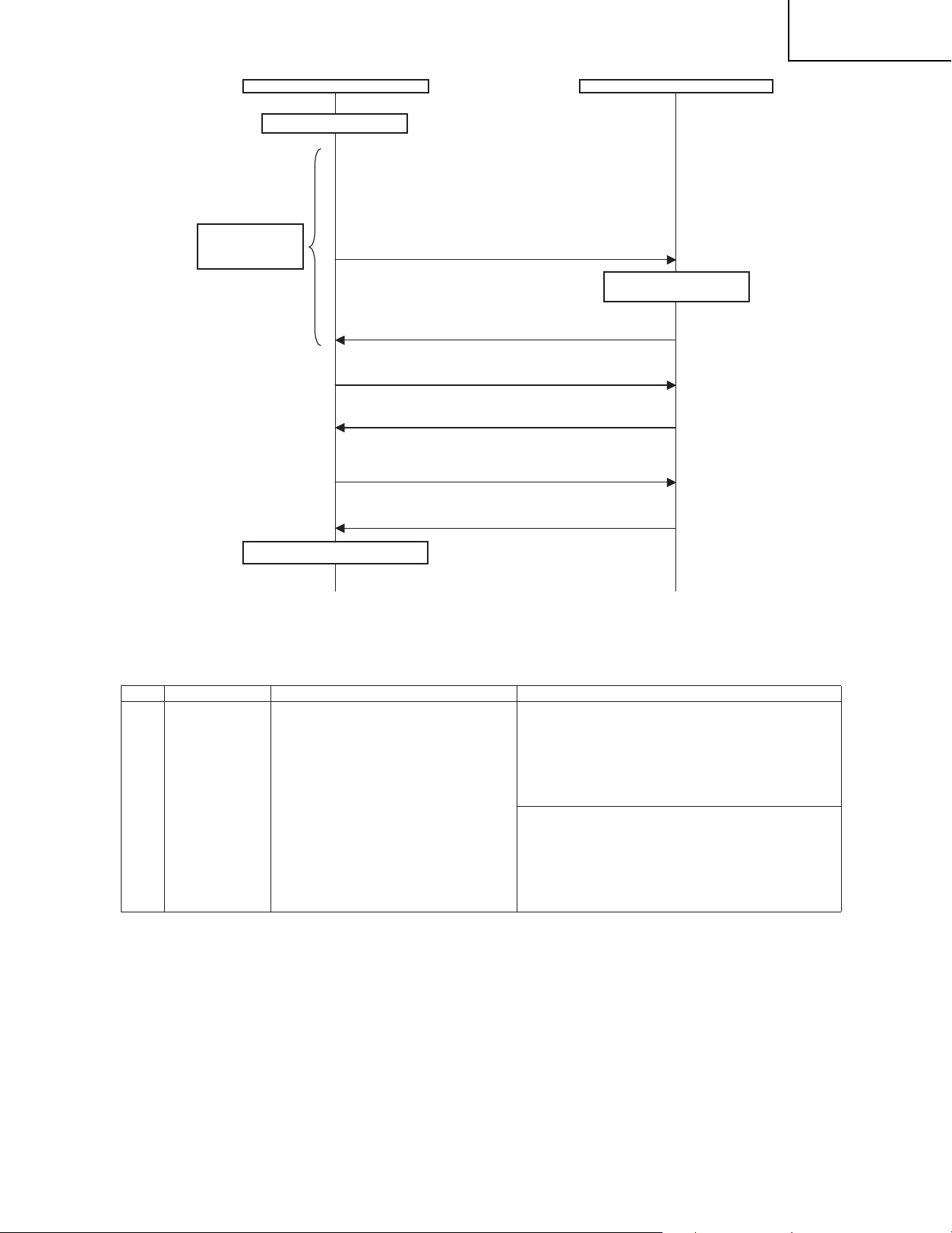
TROUBLESHOOTING TABLE
No power supply (Front LED does not light up) and no power-up even is turned on (Front LED light up to blue)
LC-20D42U
Is the AC cord connected?
Yes
Are the harness and Cable connected
properly?
Yes
Are F1 normal?
Yes
Is the voltage of C4 approx. 160V?
Yes
Are UR12V supplied?
Yes
No
Connect the AC cord and turn on the power.
No
Connect the hamess and Cable properly.
No
If the fuse is blown when turning on the power after replacing F1.replace Q1 and
PC1.
No
Check if L1,TH1 and BD1 are normal.
No
Does AC-CTRL (pin10 of CN1) become High (approx. 3.3V)?
Yes
Check the rectifier circuit of UR12V
Is the unit set to STANDBY MODE?
Is the main unit normal?
No
Is 24V supplied?
Yes
Turn on the power again,and check if
the unit works normally.
Remarks
State of the set
STDBY
MODE1
MODE2
Power ON
PS_ON
(CN1 )
High
Low
High
10
UR12V
(CN1 )
No
Do the primary side and secondary side of T1/T1A oscillate normally?
Are D20 out of order?
UR24V
1
(CN2 )
12V
--
12V
1
24V
24V
Yes
No
Are there defective parts on the primary side?Is the output on the Secondary side short-circuited?
31
Page 32

LC-20D42U
TROUBLESHOOTING TABLE (Continued)
No audio output during UHF/VHF reception
Is SIF output from the tuner (TU1101_Pin15) normal?
Yes
Is input signal fed to pin21 (SOUNDIF 1)of IC1401(SIF
Demodulator) normal?
Yes
Are audio signals from pins 29 and 30 (SC2_OUTL/R) of
IC1401 to pins 51 and 52 of IC1404 (CODEC) normal?
Yes
Are audio outputs (A-OUT_L/R) of pins 38 and 39 of
IC1404 normal?
Yes
Is audio input from pins 38 and 39 of IC1404 to pin 3 and 5
of IC2701 (STEREO_AMP) normal?
Yes
Is audio output from IC2701 normal?
Yes
Check the connector (P2703) of AV_UNIT and around the
speakers.
No
Check the tuner and peripheral circuits.
No
Check the filter circuits (Q1102-3) and peripheral
circuits
No
Check between pins 29 and 30 (SC2_OUTL/R) of
IC1401 and pins 51 and 52 of IC1404(CODEC)
Are the DSP_LRCK,DSP_BCKIN,DSP_SDIN1,
No
DSP_MCLK,DSP_SDOUT1,DSP_SDOUT2 signals
sent from IC1404 to IC1407(DSP) normally?
Yes
Check IC1404 and peripheral circuits.
No
Check the circuits between pins 38 and 39 of
IC1404 and pins 3 and 5 of IC2701. (MUTE
cercuits:Q1307,Q1314,Q1313)
No
Check IC2701 and peripheral circuits
No monitor audio output
Is monitor audio output set to "Variable"?
No
Are audio output pins 40 and 41 of IC1404 (CODEC)
normal?
Yes
Are audio output pins 7 and 1 of IC1408 (Buffer_AMP)
normal?
Yes
Check between IC1408 and MONITOR OUTPUT terminal
(J501,J502).
Yes
Reset monitor audio output to "Fixed".
No
Check IC1404 and peripheral circuits.
No
Check IC1408 and peripheral circuits.
32
Page 33

TROUBLESHOOTING TABLE (Continued)
No audio output from external input
<<HDMI>>[INPUT-4/INPUT5 (Digital audio mode)]
Is digital audio signal (DTV_SPDIF) fed from pin E12 of IC8101 to pin 4 of IC1404?
<<HDMI>>[INPUT-5(Analog audio mode)]
Is L-ch audio signal fed from pin 3 of input terminal J1501 to pin 57 of IC1404?
Is R-ch audio signal fed from pin 2 of input terminal J1501 to pin 58 of IC1404?
PCIPUT<<INPUT-6>>
Is L-ch audio signal fed from pin 2 of input terminal J1502 to pin 55 of IC1404?
Is R-ch audio signal fed from pin 3 of input terminal J1502 to pin 56 of IC1404?
<<INPUT-1>>
Is L-ch audio signal fed from input terminal J505 to pin 12 of IC1405?
Is R-ch audio signal fed from input terminal J505 to pin 1 of IC1405?
<<INPUT-2>>
Is L-ch audio signal fed from input terminal J505 to pin 15 of IC1405?
Is R-ch audio signal fed from input terminal J505 to pin 2 of IC1405?
Is L-ch audio signal fed from pin13 of IC1405 to pin 53 of IC1404?
Is R-ch audio signal fed from pin3 of IC1405 to pin 54 of IC1404?
Yes
No audio output during digital broadcasting reception
<<INPUT-3>>
Is L-ch audio signal fed from input terminal J509 to pin 4 of IC1405?
Is R-ch audio signal fed from input terminal J509 to pin 5 of IC1405?
LC-20D42U
Are the 12S signals DAKCK,SCLK,LRCK,and DATAOUT
sect from pins B22,F13,E13 and F12 of IC8101 normally?
Yes
Are input signals of pins 24 (DAKCK),11(SCLK),10(LRCK),
32(DATA) of IC1404 normal?
Yes
Are audio signals from pins 29 and 30 (SC2_OUTL/R) of IC1404 to
pin 27 and 25 of IC1407 (DSP) normal?
Yes
Are audio outputs (A-OUT_L/R) of pins 38 and 39 of IC1404 normal?
Yes
Is audio input from pins 38 and 39 of IC1404 to pins 3 and 5 of
IC2701(STEREO_AMP) normal?
Yes
Is audiio output from IC2701 normal?
Yes
No
Check around IC8101 BCM3551.
No
Check the circuits between pins B22,F13,E13 and F12 of IC8101
and pins 24,11,10 and 32 of IC1404.
No
Check between pins 29 and 30 (SC2_OUTL/R) of IC1404 and pins
27 and 25 of IC1407 (DSP).
No
Are the LRCK,BICK,SDTO and SDTI signals sent from IC1404 to
IC1407 (DSP) normally?
Yes
Check IC1403 and peripheral circuits.
No
Check the Circuits between pins 38 and 39 of IC1404 and pins 3 and
5 of IC2701.(MUTE circuits:Q1307,Q1313,Q1314)
No
Check IC2701 and peripheral circuits.
Check the connector (P2703) of AV_UNIT and around the speakers
33
Page 34

LC-20D42U
TROUBLESHOOTING TABLE (Continued)
<Component video signal input> No video output (1)
No video output from extermal input <<INPUT-1>>
Is INPUT-1 selected on the input switching menu screen?
Yes
Is video signal fed to pin 21 of IC501 (AV SWITCH)?
Yes
Is video signal sent to pin 60 of IC501?
Yes
Is video signal fed to pin K25 of IC8101 (Broadcom) via
L.P.F. composed of Q2202 and Q2210?
Yes
Are digital video (LVDS) signals sent from pins 37-42 and
45-48 of IC2602?
Are digital video (COMOS) signal sent from IC8101
(DVODATA 0-23,DVOCLKO,DVODE,DVOHSYNC,
DVOVSYNC)?
Yes
Select INPUT-1 and the input signal on the input switching
menu screen.
No
When INPUT-1 cannot be selected since the characters
INPUT-1 on the menu screen are gray.
Yes
Is the video signal detection function normal?
Check between J507 and pin 38 of IC501.
No
Check between J507 and pin 21 of IC501.
No
Check IC501 (AV SWITCH) and peripheral circuits.
No
Check between IC501 and IC3301.(Q2202,Q2210,etc.)
No
Check IC2602 and peripheral circuits.
No
Check IC8101 and peripheral circuits.
Check LCD_CONTROL PWB.
34
Page 35

TROUBLESHOOTING TABLE (Continued)
<Component video signal/S-video signal input> No video output (2)
LC-20D42U
No video output from extermal input <<INPUT-3>>
Yes
Is INPUT-2 selected on the input switching menu screen?
Yes
Is video signal fed to pin 21 of IC507 (AV SWITCH)?
<Composite video signal input>
Is video signal fed to pin 3 of IC509?
<S-video signal input>
Are Y and C signals fed to pins 5 and 7 of IC501
respectively?
Yes
<Composite video signal input>
Is video signal sent to pin 60 of IC501?
<S-video signal input>
Are Y and C signals sent to pins 60 and 59 of IC501
respectively?
Yes
No
Select INPUT-3 and the input signal on the input switching
menu screen.
No
When INPUT-3 cannot be selected since the characters
INPUT-2 on the menu.
Yes
Is the video signal detection function normal?Check
between J509 and pin 42of IC501.
Is the S-video signal detection function normal?Check
between J509 and pin 2 of IC501.
No
Check between J509 and pin 3 of IC501.
Check between J509 and pin 5 and 7 of IC501.
Check IC501 (AV SWITCH) and peripheral circuits.(Q501,
No
Q502,Q503,Q504,etc.)
Check between IC501.(Q501,Q502,Q503,Q504,etc.)
<Composite video signal input>
Is video signal fed to pin K25 of IC8101 (Broadcom) via
L.P.F. composed of Q2202 and Q2210?
<S-video signal input>
Are Y and C signals fed to pins K25 and L24 of IC8101
(Broadcom) via L.P.F. composed of Q2202 and Q2210
and via L.P.F. composed of Q2203 and Q2211
respectively?
Yes
Are digital video (LVDS) signals sent from pins 37-42 and
45-48 of IC2602?
Are digital video (COMOS) signal sent from IC8101
(DVODATA 0-23,DVOCLKO,DVODE,DVOHSYNC,
DVOVSYNC)?
Yes
Check LCD_CONTROL PWB.
Check between SC1101 and IC3301.(Q2202,Q2210,etc.)/
No
(Q2203,Q2211,etc.)
No
Check IC2602 and peripheral circuits.
No
Check IC8101 and peripheral circuits.
35
Page 36

LC-20D42U
TROUBLESHOOTING TABLE (Continued)
No video output during ANALOG broadcasting reception
Is video signal sent to output terminal pin 13 of tuner
(TU1101)?
Yes
Is video signal fed to pin 7 of IC1103 (LEVEL ADJ)?
Yes
Is video signal fed to pin R26 of IC8101 (Broadcom) via L.P.F. composed of Q2204 and Q2208?
Yes
Are digital video (LVDS) signals sent from pins 37-42 and
45-48 of IC2602?
Are digital video (COMOS) signal sent from IC8101
(DVODATA 0-23,DVOCLKO,DVODE,DVOHSYNC,
DVOVSYNC)?
Yes
Check LCD_CONTROL PWB.
No
Check or repiace the tuner's peripheral circuits.
No
Is control signal for level adjustment fed from pin 1 of
IC1104 to pin 6 of IC1103?
No
Check or replace IC1104 (CONTROL) and peripheral
circuits.
No
Check between IC1103 and IC3301.(Q2204,Q2208,etc.)
No
Check IC2602 and peripheral circuits.
No
Check IC8101 and peripheral circuits.
36
Page 37

TROUBLESHOOTING TABLE (Continued)
<Component video signal input> No video output (3)
No video output from external input<<INPUT-1>>
Is INPUT-1 selected on the input switching menu screen?
Yes
No
Select INPUT-1 and the input signal on the input switching
menu screen.
When INPUT-1 cannot be selected since the characters
INPUT-1 on the menu screen are gray.
Yes
Is the component video signal detection function normal?
Check between 6 pin of J507 and pin 38 of IC501.
LC-20D42U
Are component video signals fed to pins 21,23 and 25
(Y,Pb and Pr) of IC501 (AV SWITCH)?
Yes
Are Y,Pb and Pr signals sent to pins 60,59 and 58 of
IC501 respectively?
Yes
Are component video signals sent to R574,R580,R586 Via
the Net of Q501-Q506?
Yes
Are Y,Pb and Pr signals fed to pins L26,J25 and J26 of
IC8101 (Broadcom) respectively? Via LPF composed of
Q2202,Q2203,Q2206,Q2210,Q2211 and Q2212.
Yes
Are digital video (LVDS) signals sent from pins 37-42 and
45-48 of IC2602?
Are digital video (COMOS) signal sent from IC8101
(DVODATA 0-23,DVOCLKO,DVODE,DVOHSYHC,
DVOVSYNC)?
Yes
Check LCD_CONTROL PWB.
No
Check between J507 and each input pin of IC501.
No
Check IC501 and perpheral circuits.
No
Check between IC501 and SC501. (Q501-Q506,etc.)
No
Check IC8801.(Q2210,Q2211,Q2212,etc.)
No
Check IC2602 and peripheral circuits.
Check IC8101 and peripheral circuits.
37
Page 38

LC-20D42U
TROUBLESHOOTING TABLE (Continued)
No video output from HDMI input (INPUT4)
Are signals fed from HDMI (SC1501) connector to input
terminals H_RX0
74),H_RX2
of IC1507 (TMDS_SW)?
Are signals fed from IC1507 (TMDS_SW) to input
terminals H_RX0
and B18),H_RX2
C19 and D19) of IC8101 (Broadcom)?
Are digital video (LVDS) signals sent from pins 37-42 and
45-48 of IC2602?
Are digital video (COMOS) signal sent from IC8101
(DVODATA 0-23,DVOCLKO,DVODE,DVOHSYHC,
DVOVSYNC)?
Check LCD_CONTROL PWB.
±(pins 70 and 71),H_RX1±(pins 73 and
±(pins 76 and 77) and H_RXC±(pins 67 and 68)
±(pins B19 and A19),H_RX1±(pins A18
±(pins D18 and C18) and H_RXC±(pins
Yes
Yes
Is IC1501(E2PROM) accessed with 12C when connectiong
No
HDMI device and is DDC_12C_CLOCK/DATA data read
out?
YesYes
Check IC1501 and peripheral circuits.
Are cables connected securely?
Check the setting of HDMI device.
No
Check IC1507 (TMDS_SW) and peripheral circuits.
For INPUT4,pin 21 is Low and pin 22 is High.
No
Check IC2602 and peripheral circuits.
Check IC8101 and peripheral circuits.
No
When using an old HDMI transmission device,some video formats cannot be selected or no sound is heard. Since this model
conforms to the latest HDMI standard, the HDMI transmission device does not recognize the data of the latest version
correctly.It is necessary to upgrade its firmware. Download the latest firmware from the web site of each manufacturer,or
contact the customer service center of each manufacturer.
38
Page 39

TROUBLESHOOTING TABLE (Continued)
No video output from HDMI input (INPUT5)
LC-20D42U
Are signals fed from HDMI (SC1502) connector to input
terminals H_RX0
12),H_RX2
IC1507 (TMDS_SW)?
Are signals fed from IC1507 (TMDS_SW) to input
terminals H_RX0
and B18),H_RX2
C19 and D19) of IC8101?
Are digital video (LVDS) signals sent from pins 37-42 and
45-48 of IC2602?
Are digital video (COMOS) signal sent from IC8101
(DVODATA 0-23,DVOCLKO,DVODE,DVOHSYHC,
DVOVSYNC)?
Check LCD_CONTROL PWB.
±(pins 8 and 9),H_RX1±(pins 11 and
±(pins 14 and 15) and H_RXC±(pins 5 and 6) of
±(pins B19 and A19),H_RX1±(pins A18
±(pins D18 and C18) and H_RXC±(pins
Yes
Yes
Is IC1502 (E2PROM) accessed with 12C when connecting
No
HDMI device and is DDC_12C_CLOCK/DATA data read
out?
YesYes
Check IC1502 and peripheral circuits.
Are cables connected securely?
Check the setting of HDMI device.
No
Check IC1507 (TMDS_SW) and peripheral circuits.
For INPUT5,pin 21 is High.
No
Check IC2602 and peripheral circuits.
Check IC8101 and peripheral circuits.
No
When using an old HDMI transmission device,some video formats cannot be selected or no sound is heard. Since this model
conforms to the latest HDMI standard, the HDMI transmission device does not recognize the data of the latest version
correctly.It is necessary to upgrade its firmware. Download the latest firmware from the web site of each manufacturer,or
contact the customer service center of each manufacturer.
39
Page 40

LC-20D42U
No video output from PC input (INPUT6)
TROUBLESHOOTING TABLE (Continued)
DIGITAL mode
Analog mode
IS IC1505(E
and is DDC_12C_CLOCK/DATA data read out?
Check the setting of PC.
Are signals from pins 83-76,62-55,50-43,71-68.(DATA0-23,VSYNC,HSYNC,DE,CLK) of IC3304 (ADC) toB23,A23,D22,C22,
E23,A25,D23,B24,F22,A24,C23,E22,D17,F18,E18,F17,E17,C17,B17,A17,C16,D16,F16,E16 ,F23,G22,C25,C24 of IC1801?
Are digital video (LVDS) signals sent from pins 37-42 and
45-48 of IC2602?
Are digital video (COMOS) signal sent from IC8101
(DVODATA0>23,DVOCLKO,DVODE, DVOHSYHC,
DVOVSYNC)?
Check LCD_CONTROL PWB.
2
PROM) accessed 12C when connecting PC
Yes
Check IC1505 and peripheral circuits.Are cable connected securely?
Yes
Yes
No
Are signal fed from pins 1,2,3(Analog-R/G/B),and 13,14(H
Yes
Sync/V Sync) of input terminal (SC1503) to pins 11,9,6,2,3
of IC3304 (A/DC)?
Yes
Check peripheral circuits of IC3304
Check connection of IC3304 and IC8101.
No
Check IC2602 and peripheral circuits.
No
Check IC8101 and peripheral circuits.
No
No
When using an old HDMI transmission device,some video formats cannot be selected or no sound is heard. Since this model
conforms to the latest HDMI standard, the HDMI transmission device does not recognize the data of the latest version
correctly.It is necessary to upgrade its firmware. Download the latest firmware from the web site of each manufacturer,or
contact the customer service center of each manufacturer.
[FRONT-END SECTION]
Digital broadcasting cannot be received.
Yes
Are IF_OUT_P/N signal send from
pin (20) (19) of TU1101 respectively?
No
Check the TU1101.
Yes
Are signal fed to pins U25,U26 of
IC8101?
No
Check between TU1101 and
IC8101(C1104,C1141,etc.).
Yes
Check IC8101 and its peripheral circuits.
40
Page 41

TROUBLESHOOTING TABLE (Continued)
LED flashing timing chart for error notification
1) Red power LED
Remarks
Remarks
Remarks
Error type Power green LED operation (1 cycle)
Error type OPC LED operation (1 cycle)
Error type OPC LED operation (1 cycle)
Pins are monitor microprocessor pins.
H: On
L: Off
H: On
L: Off
H: On
L: Off
H: On
L: Off
H: On
L: Off
H: On
L: Off
H: On
L: Off
H: On
L: Off
H: On
L: Off
H: On
L: Off
H: On
L: Off
H: On
L: Off
Refer to "Power failure details".
Power failure
Flashes twice
communication failure
Refer to "Communication failure details".
with main CPU
Communication line failure or main CPU communication failure > Check debug statements for the main CPU.
Flashes 3 times
Vsync
failure
Flashes 4 times
Monitor temperature failure
Flashes 5 times
2) Power failure details (Power LED flashes twice and OPC LED flashes)
Pins are monitor microprocessor pins unless otherwise specified.
DET_10V failure
Flashes once
DET_D3.3V failure
Flashes twice
DET_6V failure
Flashes 3 times
Panel 5V failure
Flashes 5 times
Main failure
Flashes 7 times
3) Communication failure details (Power LED flashes 3 times and OPC LED flash
Initial communication
reception failure
Flashes once
Time-out setting reception failure
Start-up confirmation reception failure
Flashes twice
Regular communication failure
Flashes 3 times
The details are displayed in "ERROR STANDBY CAUSE" on page 1 of process A mode for the main microprocessor.
Initial communication from the main CPU is not received. (After canceling the reset, request for the monitor model No. is not received.)
Communication line failure or main CPU start-up failure
Time-out setting and start-up mode change cannot be received from the main CPU. (Start-up communication until time-out setting and
startup mode change is not received.)
Basically, communication logs are analyzed by a bus monitor or debug print logs are analyzed.
Main CPU start-up failure or monitor microprocessor's reception failure
Regular communication that is performed at 1 second intervals in the normal operation is interrupted.
Main CPU operation failure or monitor microprocessor's reception failure
Main microprocessor detection error,
DET_PNL5V (pin 58): Abnormal (L). Panel power is not applied.
If error is detected during operation, error standby is activated by polling.
EU_POW
PS_ON
PANEL_POW
D_POW
If error is detected during operation, error standby is activated by polling.
DET_6V (pin 56): Abnormal (L). D5V,A5V is not applied.
(MONITOR MAX TEMP on process A mode: Change of temperature failure AD value): Thermistor
If error is detected during operation, error standby is activated by polling.
AC_DET (pin 16): Abnormal (L), DET_10V (pin 57). Main converter A9V/UR10V is not applied.
If error is detected during operation, the power is turned on again by interrupt handling (instantaneous blackout processing).
DET_3V3 (pin 59): Abnormal (L). Main power 3.3V is not applied.
VSYNC (pin 46) failure (uninput). Video process operation failure.
Detected during operation (interruption)
If the panel temperature is 60˚C or more for 15 seconds or more in a row, CAUTION appears on the OSD of AVC (flashes in red in the
lower right screen).
If the panel temperature is 60˚C or more for 25 seconds or more in a row, error standby is activated.
MAIN CPU communication: TXD(28pin),RXD(29pin).
H: On
L: Off
Program DATA broken
Flaches & times.
Recovery: Mcu flash ROM DATA failure.
Mcu SOFT rewrite.
>
>
>
LC-20D42U
41
Page 42

LC-20D42U
IXB870WJQZ BALLOUT
1-1. IC8101 (RH-iXB870WJQZQ)
This IC is a system LSI with the following function.
A cable,ground wave receiver,NTSC decoder,HDMI receiver,transport processor,MPEG video pocessor,digital
andio decoder,analog video processor,graphics processor,MLPS processor, and Peripheral controller.
IXB870WJQZ BALLOUT
123456789101112 13 14 15 16 17 18 19 20 21 22 23 24 25 26
TMODE_
A GND GPIO_54
DDR_VD
B
GPIO_51
DP
DDR0_V
DDR_BV
C
REF1
DDR_1
DDR0_D
DDR0_D
D
ATA26
ATA24
DDR0_D
DDR0_D
E
ATA31
ATA30
DDR0_D
DDR0_D
F
ATA17
ATA16
DDR0_D
DDR0_D
G
ATA23
ATA21
DDR0_WEBDDR0_C
H
J
K GND
L
M
N
P
R
T
U GND
V
W
Y
AA
AB
AC
AD GPIO_30 GPIO_10GPIO_05
AE GPIO_06 VDDO
AF GND
ASB
DDR0_BA0DDR0_BA1DDR0_R
DDR0_A
DDR01
DDR_VDDPDDR0_A
DDR05
DDR0_A
DDR0_A
DDR07
DDR06
DDR0_C
DDR0_C
LK0
LK0B
DDR0_D
DDR0_D
ATA10
ATA12
DDR0_D
DDR0_D
ATA15
ATA00
DDR0_D
DDR0_D
ATA03
ATA05
DDR0_V
REF0
DDR_VDDPDDR_BV
DDR_2
USB_DP1USB_DN1USB_PW
USB_MO
USB_PW
NCDR
RON_1
USB_RREFPKT1_D
ATA
POD_PK
POD_PK
T5P_CL
T5P_DA
K
TA_2
POD_PK
POD_PK
T5P_DA
T5P_DA
TA_4
TA_7
HSX_CL
DVO_27 DVO_21 DVO_17 DVO_12 DVO_7 DVO_DE
1
TMODE_3TMODE_
DDR_PV
GPIO_52 DVO_28 DVO_22 DVO_16 DVO_11 DVO_5 DVO_1
SSP
DDR_BV
GPIO_50
SSR_1
DDR0_D
UART_R
ATA28
XD_2
DDR0_D
DDR0_D
ATA27
ATA25
DDR0_D
DDR0_D
ATA19
DDR0_D
DDR0_D
ATA18
DDR0_C
ASB
DDR0_A
DDR0_A
DDR00
DDR10
DDR0_A
DDR0_A
DDR04
DDR08
DDR0_A
DDR0_CKEDDR0_D
DDR12
DDR0_D
DDR0_D
ATA08
ATA13
DDR0_D
DDR0_DM0DDR0_D
ATA14
DDR0_D
DDR0_D
ATA01
ATA04
DDR0_D
USB_AV
ATA06
DD33
DDR_BV
USB_XT
SSR_2
USB_AV
PKT0-
DD12PL
DATA
L
PKT0_S
RFLT_1
YNC
POD_PK
PKT1_C
T5P_VA
LK
POD_PK
POD_PK
T5P_DA
T5P_DA
TA_0
TA_5
GPIO_29GPIO_55
GPIO_11GPIO_07
POD_PS
_CLK
POD_PS
HSX_DA
_DATA_
TA
PLL_MIP
PLL_MIP
S_AVDD
K
S_AGND
1P2
MAJOR IC INFORMATIONS
VDDO GND DVO_14 DVO_10 DVO_4
0
TMODE_
DVO_25 DVO_19 DVO_13 DVO_6 DVO_2
2
GPIO_53 DVO_29 DVO_23 DVO_15 DVO_8 DVO_3
DDR_CLKUART_T
DDR0_D
QS3
ATA29
DDR0_DM2DDR0_DM3DDR_VD
QS2
DDR0_D
SB0
ATA22
DDR0_A
DDR02
DDR0_A
DDR09
ATA09
DDR0_D
DDR0_D
ATA07
USB_XT
PKT0_CLKPKT1_S
ALI
NO_CON
NECT
POD_PK
T5P_SY
POD_PK
T5P_DA
LID
TA_6
GPIO_56GPIO_09
HSX_SYNCPOD_PS
POD_PS
_SYNC
POD_PS
_DATA_
POD_OB
_CLK
2
PCI_RSTBPCI_GN
DVO_26 DVO_20 DVO_9 DVO_0
XD_2
DDR_PV
DVO_24 GND DVO_18
DDP
DP
DDR0_D
GND VDDC VDDC VDDC VDDC VDDC VDDC VDDC VDDC VDDC VDDC VDDP GND GND GND GND
ATA20
DDR0_A
DDR_VD
DDR03
DP
DDR0_A
GND VDDC GND GND GND GND GND GND GND GND GND VDDC VDDO VDDO
DDR11
DDR0_D
DDR_VD
ATA11
DP
DDR0_D
QS1
QS0
ALO
NC
GND VDDC GND GND GND GND GND GND GND GND GND VDDC VDDO
M1
DDR0_D
DDR_VD
ATA02
DP
USB_AV
USB_MO
DD25PL
NPLLCD
L
R
USB_AGNDUSB_AV
DD12
VDDC VDDC GND GND GND GND GND GND GND GND GND VDDC VDDO GND
YNC
POD_PK
VDDC VDDC VDDC VDDC VDDC VDDC VDDC VDDC VDDC VDDC VDDC VDDC VDDO GND GPIO_25 GPIO_48GPIO_47
T5P_DA
TA_1
POD_PK
VDDC VDDC VDDO VDDO VDDO VDDO VDDO VDDO VDDO VDDO VDDO VDDO VDDO GND GPIO_19 GPIO_24GPIO_35 GPIO_46OB_AGC
T5P_DA
TA_3
GPIO_31GPIO_08 GND
POD_PS
_DATA_
0
POD_PS
_DATA_
_VAL
5
POD_PS
BYP_CP
_DATA_
U_CLK
4
POD_OB
PCI_CLK
_DATA
_OUT
3
PCI_CLK
PCI_AD30PCI_VIO
_IN
PCI_AD21PCI_AD29PCI_AD28PCI_AD24PCI_FRA
T2B
VDDO VDDP VDDO VDDP VDDO VDDO VDDO VDDO VDDO VDDO VDDO VDDP GND GND GND
VDDC GND GND GND GND GND GND GND GND GND VDDC VDDO GND GND
VDDC GND GND GND GND GND GND GND GND GND VDDC VDDO
VDDC GND GND GND GND GND GND GND GND GND VDDC VDDO
VDDC GND GND GND GND GND GND GND GND GND VDDC VDDO
VDDC GND GND GND GND GND GND GND GND GND VDDC VDDO VDDP GND
POD_PS
_DATA_6GND
PLLTES
T_MIPS
PCI_AD22PCI_AD1
PCI_AD20PCI_AD17PCI_AD27PCI_TRDYBPCI_CBE01PCI_AD15PCI_AD09PCI_INT
_1
DVO_CL
SPDIF_I
K_POS
N_P
DVO_CL
SPDIF_I
K_NEG
N_N
DVO_VS
YNC
DVO_HS
YNC
SGPIO_06AUD_SP
SGPIO_0712S_DA
SPDIF_A
SPDIF_A
VDD2P5
VSS
POD_PS
POD_PS
_DATA_
PCI_RE
Q2B
VDDO GND
VDDO VDDO VDDO VDDO VDDO
_DATA_
1
7
PCI_AD31PCI_AD16PCI_AD23PCI_DE
PCI_AD19PCI_AD26PCI_CBE
PCI_AD25PCI_CBE03PCI_SERRBPCI_AD11PCI_INT
VDDO
8
PCI_IRDYBPCI_PERRBPCI_CBE00PCI_AD1
MEB
AUD_RI
GHT_P
AUD_RI
GHT_N
AUD_RV
DDO3P3
AUD_RV
SSO
DIF
TA_OUT
GND VDDO
02
PCI_STO
PB
AUD_LE
VDAC0_0VDAC_B
FT_N
AUD_LE
VDAC0_3VDAC_R
FT_P
AUD_LV
VDAC0_
DDO3P3
AUD_LV
VDAC0_2VDAC_A
SSO
12S_LR_
VDAC_A
OUT
12S_CLK
VDAC_A
_OUT
VDAC_A
VDD3P3
PCI_AD13PCI_AD0
VSELB
PCI_AD1
PCI_PAR
PCI_AD14PCI_AD07PCI_AD06PCI_VIO_2PCI_INT
VDDO
VSS
VSS
1
2
0
GVSS
BIAS
VDAC_B
GVDD1P
2
VDD2P5
VDAC_D
VSS
VDAC_D
VDD1P2
VDAC_A
VDD3P3
8
PCI_AD0
3
_A1
_A0
GND VDDO
GPIO_41GPIO_04
GPIO_40GPIO_03
GPIO_12GPIO_02
GPIO_36GPIO_42
GPIO_38GPIO_01 GPIO_45 GND
GPIO_37GPIO_00 GPIO_44
GPIO_39 VDDO
EBI_CS3BEBI_TSI
VDDP
GND
PCI_AD04EBI_RDBEBI_WE
PCI_AD05PCI_GN
HDMI_D
HDMII_
HDMI_D
ATA_0_
ATA_1_P
HDMI_D
HDMI_D
ATA_1_
ATA_0_P
N
HDMI_D
HDMI_C
ATA_2_
LK_P
N
HDMI_D
HDMI_C
ATA_2_P
LK_N
DVOPLL
_AVDD1
DVOPLL
GND
_AVSS
GND GND GPIO_14 GPIO_15GPIO_20 GPIO_26GPIO_34
ZE1B
EBI_RWBEJTAG_
EBI_CS0BEBI_TABEJTAG_
PCI_INT
GPIO_59 RESETBGPIO_13 GPIO_16GPIO_21 GPIO_27GPIO_49
TCK
TMS
EBI_TSB
1B
EBI_CS1BEBI_CS4BEBI_DSBEJTAG_
VDDO
T0B
PCI_AD02PCI_RE
_A2
PCI_AD01PCI_AD00PCI_GN
_A3
HDMII_
N
P2
Q0B
HTPLG_
HDMII_
HTPLG_I
HDMII_
DDC_SD
HDMI_R
XVDD3P
HDMI_A
HDMI_R
ESREF
HDMI_P
LL_AVD
SD_AVD
OB_AVSSOB_AVD
CLK54_
AVSS
EDSAFE
_ADCD_
GPIO_57GPIO_61
EBI_AD
DR24
PCI_RE
12S_CLK
DDC_SC
OUT
L
12S_LR_
GPIO_43
IN
N
12S_DA
HD_DVI_3HD_DVI
TA_IN
A
HDMII_
HD_DVI_2HD_DVI_6HD_DVI
CEC
3
HDMI_R
HD_DVI
XVDD2P
VSS
5
HDMI_R
HD_DVI_8HD_DVI
XVDD1P
2
HD_DVI
VDDO
_HSYNC
D1P2
SD_AVD
SD_AVD
SD_AVD
D_AFE2
P5
SD_AGNDSD_AVD
D1P2
OB_DVSSOB_AVD
D1P2
EDSAFE
EDSAFE
_PLLGN
D
EDSAFE
EDSAFE
_AVDD2
_AGND
GND
BYP_DS
SGPIO_02SGPIO_03AGC_VDDOSGPIO_04EDSAFE
BSC_S_SCLBSC_S_S
EJTAG_
GPIO_58
TDO
EBI_WE0BEBI_TA2BEJTAG_
Q1B
EBI_CS2BEBI_TSI
T1B
D_AFE2
_PLLVD
HD_DVI_1HD_DVI_9HD_DVI
_IN
HD_DVI_0HD_DVI
_10
HD_DVI
_11
_4
_VSYNC
GND
VCXO_A
GND
PLL_MA
IN_AGN
D
SD_AVD
D_CLK2
D1P2
P5
SD_AVD
D_CLK2
P5
P5
SD_AGNDOB_DVD
D1P2
D2P5
CLK54_
AVDD2P
D1P2
5
EDSAFE
_AVDD1
P5
P2
EDSAFE
_AVDDT
_CLK
H1P2
DA
RESET_
OUTB
IR1_IN GPIO_60 GPIO_17GPIO_23 AD
TDI
TRSTB
ZE0B
_5
VDDO
_7
HD_DVI
HD_DVI
_CLK_P
_DE
VCXO27_BANT_RX
_CLK_N
BYP_SY
GND
S108_CL
K
ANT_DETANT_TX
_DATA
PLL_MA
VCXO_A
IN_AGN
VDD1P2
D
VCXO_A
SD_INC
GND
M_CVBS
NO_CON
SD_PB SD_PR J
NECT
SD_AGN
SD_Y
D
SD_INC
SD_C
M_LC
OB_IFV
D1P2
CO_N
CLK54_
OB_I_N OB_I_P N
AVDD1P
2
EDSAFE
CLK54_
_ADCD_
XTAL_N
VDD1P2
EDSAFE
EDSAFE
_CLKVD
_VCM_0
D2P5
EDSAFE
EDSAFE
_ADCVD
_VCM_1
D2P5
_IF_N
DS_AGC
NO_CON
I_CTL
NECT
SGPIO_01SGPIO_0
VDDP GPIO_28GPIO_33 AB
NMIB GPIO_22 GPIO_32 AC
IR_OUT IR2_IN GPIO_18 AE
EBI_AD
VDDO GND AF
DR25
GND A
BYP_SY
S9_CLK
VCXO27
_A
_DATA
PLL_MA
IN_AVD
D1P2
PLLTES
T_MAIN
GND G
SD_CVB
S
SD_INC
M_COMPK
SD_L L
OB_IFV
CO_P
CLK54_
XTAL_P
EDSAFE
_CVBS_
0
EDSAFE
_CVBS_
1
EDSAFE
_IF_P
NO_CON
NECT
DS_AGC
T_CTL
5
SGPIO_0
0
B
C
D
E
F
H
M
P
R
T
U
V
W
Y
AA
42
Page 43

--MEMO--
LC-20D42U
43
Page 44

LC-20D42U
Disclete LPF
IC1301
I/O
M62320
<MUTE>
IC1404
CODEC AK4683
IC8101
IXB870WJQZ
MAIN
I2C0
PCI/LOCAL BUS
SPDIF
Digital Audio
UART
SP
P2703(4p)
IC8454
EEPROM
BR24L64F
I2CEXT
HDMI 2
P9005
BUS Connecter
USB
IF
DTV_HDMI/I2S
DTV/SPDIF
SIF
IN1
IC2701
Digital AMP
TPA3101D
SP_L/SP_R
DTV_SPDIF
Tuner L/R
IN2
IN3
RX0
OUT1
OUT2
SDTOA
SDTIA2
SDTIA3
TX
HDMI 1
24-bit Digital
D3.3V
D2.6V
Y
C
RGB 24 bit
CK,HD,VD,DE
RF IN
DIF
AGC
RGB
RGB_LR
OPTICAL
OUT
IC1507
TMDS
Selector
TMDS341A
TUN_I2C
IN4
IC8452
NOR FLASH
64Mb
CVBS
RX_x8
RX_x8
RGB
I2C_0
I2C_1
(100KHz)
3.3V
HD,VD
D3.3V
IC1401
Voice
multiplex
decoder
AN5832SA
AFT
RGBAudio
(Mini Plug)
INPUT
6
4
5
6
RX1
SDTIB
EEPROM
RESET
To CPLD
A_OUT_SW
DTV_SPIDF
DTV_I2S
IC1104
DAC
M62332FP
I2C1
(100KHz)
5V
+5V
GAIN
EA[23:1
Tuner I2C
IF_AGC
D1.2V
Analog RGB
HD,VD
Digital IN
DVIDATA[23:0]
DVICLK
DVIHSYNC
DVIVSYNC
DVIDE
DS_AGCI_CTL
Digital Out
DVO DATA[23:0]
DVOCLK0
DVOCLK1
DVODE
DVOHSYNC
DVOVSYNC
DVODE
EDSAFE_CVBS_0
SD_L
SD_CVBS
FCLK
CVBS
SD_PB
SD_PR
SD_C
TMDS_SEL_D[2:0]
TMDS_SEL_CLK
HDMI_DATA[2:0]
HDMI_CLK
IC3304
RGB ADC
Mstar
3ch 10bit
ADC
(2mux/ch)
108MHz
1080i
85.5MHz
WXGA
HDMI_I2C
I2S_IN
I2S_OUT
X3301
14.318MHz
SD_Y
Y
Cb
Cr
+3.3V
+2.5V
IC1103
AMP
I2C_2
(400KHz)
3.3V
IC8451
EEPROM
B979WJ
EEPROM
D5V
D5V
A5V
D3.3V
+5V
D5V
D5V
A5V
D3.3V
UR6V
D3.3V
D3.3V
33
I2C_BSC
UART
CVBS
HDMI_L/R
HDMI Audio
5
EEPROM
D5V
IC1504
1ShotMulti
VD
To M16
UART
P9301
Connector for
software
writing
I/O
EDSAFE_IF_P
EDSAFE_IF_N
EDSAFE_CVBS_1
1ch 12bit
ADC
(3mux/1ch)
108MHz
1080i
BU5V
Audio
Out
L/R
A9V
CVBS
CVBS
L/R
CVBS
S
IC501
AV SWITCH
MM3151XQ
Monitor
Out
TV
Main
Out
Video3
Video1
Video2
CVBS
S Video
2
3
1
L/R
L/R
IC1407
SOUND DSP
TAS3108D
IC1405
Analog SW
D2.6
Port(OUT)
SC8401
USB
IC8401
Power
+UR6V
Component
CVBS/LR
YPbPr
IC1402
EEPROM
B991WJ
TU1101
Analog/Digital
Tuner
+5V
LR
CVBS/LR
+12V
+5V
MOBILE Audio_LR
IN5
30MHz
7MHz
7MHz
7MHz
7MHz
30MHz
30MHz
BLOCK DIAGRAM
H
G
E
D
C
B
F
A
87109654321
44
Page 45

LV P2601
(32p FFC)
UART
AC
80 FFC
Inverter
POWER
MENU
INPUT
CH-UP/DOWN
VOL-UP/DOWN
KEY
KM
(P2002 4p)
LCD
CN2
(10p)
PNL+5V
LB P2603
(5pin )
+24V
PNL+5V
KEY1,KEY2
PS_ON/AC_CTRL
SH P2602
(7pin )
AC_DET
PD
P9701(12PIN)
RA P101(15p)
LED
OPC_LED,POW_LED_R,POW_LED_G
R/C
OPC
LED
USB
24-bit Digital
R/C
R/L,U/D
Power
MAIN
A9V
A5V
D5V
D3.3V
D2.6V
D1.2V
IC9101
CPLD
B860WJ
D3.3V
DET_PNL5V,DET_10V,DET_6V
LED(3)
STBY_POW
CN103
(14pin )
BU+3.3V
BU+5V
OPC
R/C
+12V
BackUp
BU+3.3V
D_POW,PNL5V_ON
RESET
54.000MHz
RA (P502 15p)
BU+3.3V
EA[23:1] ED[15:0]
ut
TA[23:0]
X8101
X'tal
54MHz
FCLK
IC2002
CPU
M16
BU+3.3V
X2001
X'tal
I2C
A/D(2)
A/D
A/D
INT0
PM_REQ
SRESET
CBOOTS
20MHz
IC2001
Reset
UART
TEMP[3:0],O/S_SET,FRAME
TH2001
Thermister
Von
I2C
AC_DET
Vbrt
THERMO
SW
SW
IC8301
IC8302
DDR-SDRAM
256Mbit*2
DDR-400
AFT
33.0MHz
RESET
INT
SRESET
RESET
I2C_BSC
I/O
I/0
32KHz
X'tal
32.728KHz
I/O
I/O
P9201
Board Config
SC8401
USB
IC8401
Power
+UR6V
Mobile
Audio
Board Config
Wire
Detect
5V_REG
BU+3.3V
BackUP
C
IC2005
DAC
M62332FP
IC2602
LVDS Tx
VHIV385AGLF-1Y
$0.51
D3.3V
IC2004
EEPROM
BR24L08F
D3.3V
BU+3.3V
BU+3.3V
+2.6V
BU+5V
LC-20D42U
45
1716 1918151413121110
Page 46

LC-20D42U
P2002P2002
P2703P2703
MAIN UNITMAIN UNIT
QCNW-F193WJQZ QCNW-F193WJQZ
LC-20D42ULC-20D42U
OVERALL WIRING DIAGRAMO V E R A L L W I R I N G D I A G R A M
P151P151
KEY UNITKEY UNIT
1 4
P502P502
QCNW-F723WJPZ QCNW-F723WJPZ
QCNW-F727WJQZ QCNW-F727WJQZ
QCNW-F726WJQZ QCNW-F726WJQZ
QCNW-F724WJQZ QCNW-F724WJQZ
QCNW-F206WJQZ QCNW-F206WJQZ
J1501J1501
J507J507
J509J509
J505J505
J501J501
SC1503SC1503
D1306D1306
J1502J1502
SC1501SC1501
SC8401SC8401
SC1502SC1502
1 4
1 4
1 15
P2602P2602
P9701P9701
P2603P2603
P2601P2601
1 12
1 5
1 7
1 32
CN1
CN2
LCD CONTROL UNIT
POWER
UNIT
CN1CN1
1 12
P101P101
LED UNITLED UNIT
15 1
1
2
3
5
6
7
OVERALL WIRING DIAGRAM
H
G
F
E
D
C
B
A
46
87109654321
Page 47

LC-20D42U
INVERTERINVERTER
UNITUNIT
CN103CN103
QCNW-F725WJQZ QCNW-F725WJQZ
To LAMP
To LAMP
To LAMP
To LAMP
To LAMP
80
80
CN1CN1
CN2CN2
LCD CONTROL UNITLCD CONTROL UNIT
1 7
1 32
1 14
POWERPOWER
UNITUNIT
CN1CN1
AC INAC IN
CN2CN2
1 12
1 10
4
1716 1918151413121110
47
Page 48

LC-20D42U
DESCRIPTION OF SCHEMATIC DIAGRAM
VOLTAGE MEASUREMENT CONDITION:
1. The voltages at test points are measured on the
stable supply voltage of AC 120V. Signals are fed
by a color bar signal generator for servicing purpose
and the above voltages are measured with a 20k
ohm/V tester.
INDICATION OF RESISTOR &
CAPACITOR:
RESISTOR
1. The unit of resistance “Ω” is omitted.
(K=kΩ=1000 Ω, M=MΩ).
2. All resistors are ± 5%, unless otherwise noted.
(K= ± 10%, F= ± 1%, D= ± 0.5%)
3. All resistors are 1/16W, unless otherwise noted.
CAPACITOR
1. All capacitors are µF, unless otherwise noted.
(P=pF=µµF).
2. All capacitors are 50V, unless otherwise noted.
CAUTION:
This circuit diagram is original one, therefore there may be a
slight difference from yours.
SAFETY NOTES:
1.DISCONNECT THE AC PLUG FROM THE AC
OUTLET BEFORE REPLACING PARTS.
2.SEMICONDUCTOR HEAT SINKS SHOULD BE
REGARDED AS POTENTIAL SHOCK HAZARDS
WHEN THE CHASSIS IS OPERATING.
IMPORTANT SAFETY NOTICE:
PARTS MARKED WITH “å” ( ) ARE
IMPORTANT FOR MAINTAINING THE SAFETY OF
THE SET. BE SURE TO REPLACE THESE PARTS
WITH SPECIFIED ONES FOR MAINTAINING THE
SAFETY AND PERFORMANCE OF THE SET.
AVIS DE SECURITE IMPORTANT:
LES PIECES MARQUEES “å” ( )SONT
IMPORTANTES POUR MAINTENIR LA SECURITE
DE L'APPAREIL.
NE REMPLACER CES PIEDES QUE PAR DES
PIECES DONT LE NUMERO EST SPECIFIE POUR
MAINTENIR LA SECURITE ET PROTEGER LE BON
FONCTIONNEMENT DE L'APPAREIL.
Note: MAIN 14,15 does not use it.
48
Page 49

SCHEMATIC DIAGRAM
Ë
LED Unit
H
G
F
LC-20D42U
E
D
C
B
A
654321
49
Page 50

LC-20D42U
Ë
MAIN Unit-1/20
H
G
F
E
D
C
B
A
87109654321
50
Page 51

LC-20D42U
51
1716 1918151413121110
Page 52

LC-20D42U
Ë
MAIN Unit-2/20
H
G
F
E
D
C
B
A
87109654321
52
Page 53

LC-20D42U
53
1716 1918151413121110
Page 54

LC-20D42U
Ë
MAIN Unit-3/20
H
G
F
E
D
C
B
A
87109654321
54
Page 55

LC-20D42U
55
1716 1918151413121110
Page 56

LC-20D42U
Ë
MAIN Unit-4/20
H
G
F
E
D
C
B
A
87109654321
56
Page 57

LC-20D42U
57
1716 1918151413121110
Page 58

LC-20D42U
Ë
MAIN Unit-5 /20
H
G
F
E
D
C
B
A
87109654321
58
Page 59

LC-20D42U
59
1716 1918151413121110
Page 60

LC-20D42U
Ë
MAIN Unit-6 /20
H
G
F
E
D
C
B
A
87109654321
60
Page 61

LC-20D42U
61
1716 1918151413121110
Page 62

LC-20D42U
Ë
MAIN Unit-7 /20
H
G
F
E
D
C
B
A
87109654321
62
Page 63

LC-20D42U
63
1716 1918151413121110
Page 64

LC-20D42U
Ë
MAIN Unit-8 /20
H
G
F
E
D
C
B
A
87109654321
64
Page 65

LC-20D42U
65
1716 1918151413121110
Page 66

LC-20D42U
Ë
MAIN Unit-9 /20
H
G
F
E
D
C
B
A
87109654321
66
Page 67

LC-20D42U
67
1716 1918151413121110
Page 68

LC-20D42U
Ë
H
G
F
MAIN Unit-10 /20
E
D
C
B
A
87109654321
68
Page 69

LC-20D42U
69
1716 1918151413121110
Page 70

LC-20D42U
Ë
H
G
F
MAIN Unit-11 /20
E
D
C
B
A
87109654321
70
Page 71

LC-20D42U
71
1716 1918151413121110
Page 72

LC-20D42U
Ë
H
G
F
MAIN Unit-12 /20
E
D
C
B
A
87109654321
72
Page 73

LC-20D42U
73
1716 1918151413121110
Page 74

LC-20D42U
Ë
MAIN Unit-13/20
H
G
F
E
D
C
B
A
87109654321
74
Page 75

LC-20D42U
75
1716 1918151413121110
Page 76

LC-20D42U
Ë
H
G
F
MAIN Unit-14 /20
E
D
C
B
A
87109654321
76
Page 77

LC-20D42U
77
1716 1918151413121110
Page 78

LC-20D42U
Ë
H
G
F
MAIN Unit-15 /20
E
D
C
B
A
87109654321
78
Page 79

LC-20D42U
79
1716 1918151413121110
Page 80

LC-20D42U
Ë
H
G
F
MAIN Unit-16 /20
E
D
C
B
A
87109654321
80
Page 81

LC-20D42U
81
1716 1918151413121110
Page 82

LC-20D42U
Ë
H
G
F
MAIN Unit-17 /20
E
D
C
B
A
87109654321
82
Page 83

LC-20D42U
83
1716 1918151413121110
Page 84

LC-20D42U
Ë
H
G
F
MAIN Unit-18 /20
E
D
C
B
A
87109654321
84
Page 85

LC-20D42U
85
1716 1918151413121110
Page 86

LC-20D42U
Ë
H
G
F
MAIN Unit-19/20
E
D
C
B
A
87109654321
86
Page 87

LC-20D42U
87
1716 1918151413121110
Page 88

LC-20D42U
Ë
MAIN Unit-20/20
H
G
F
E
D
C
B
A
87109654321
88
Page 89

LC-20D42U
89
1716 1918151413121110
Page 90

LC-20D42U
Ë
H
G
F
KEY Unit
E
D
C
B
A
87109654321
90
Page 91

LC-20D42U
91
1716 1918151413121110
Page 92

LC-20D42U
PRINTED WIRING BOARD ASSEMBLIES
H
G
LED Unit (Side-A)
F
E
D
LED Unit (Chip Parts Side-A)
C
B
A
LED Unit (Side-B)
87109654321
92
Page 93

LC-20D42U
93
1716 1918151413121110
Page 94

LC-20D42U
H
G
F
E
D
C
B
A
MAIN Unit (Side-A)
87109654321
94
Page 95

LC-20D42U
95
1716 1918151413121110
Page 96

LC-20D42U
H
G
F
E
D
C
B
A
MAIN Unit (Chip Parts Side-A)
87109654321
96
Page 97

LC-20D42U
97
1716 1918151413121110
Page 98

LC-20D42U
H
G
F
E
D
C
B
A
MAIN Unit (Side-B)
87109654321
98
Page 99

LC-20D42U
99
1716 1918151413121110
Page 100

LC-20D42U
H
G
F
E
D
C
B
A
MAIN Unit (Chip Parts Side-B)
87109654321
100
 Loading...