

Page 1

SERVICE MANUAL
In the interests of user-safety the set should be restored to its
original condition and only parts identical to those specified be
used.
No. S3529HTX1U///
HOME THEATER WITH DVD
HT-X1
CONTENTS
CHAPTER 1. GENERAL DESCRIPTION
[1] Specifications ................................................. 1-1
[2] Names of parts............................................... 1-2
CHAPTER 2. ADJUSTMENTS
[1] TEST Mode .................................................... 2-1
CHAPTER 3. MECHANISM BLOCKS
[1] Caution on diassembly................................... 3-1
CHAPTER 4. DIAGRAMS
[1] Block diagram ................................................ 4-1
CHAPTER 5. CIRCUIT DESCRIPTION
[1] Notes on schematic diagram.......................... 5-1
[2] Types of transistor.......................................... 5-1
[3] Waveforms of circuit....................................... 5-2
[4] Voltage ........................................................... 5-3
MODEL
HT-X1 Home Theater with DVD consisting of HT-X1 (main
unit and subwoofer/amplifier unit), CP-X1F (front speakers),
CP-X1C (center speaker) CP-X1S (surround speakers).
CHAPTER 6. CIRCUIT SCHEMATICS AND PARTS
LAYOUT
[1] Schematic diagram........................................6-1
[2] Wiring side of PWB...................................... 6-11
[3] DVD PWB Unit ............................................6-18
CHAPTER 7. FLOWCHART
[1] Troubleshooting.............................................7-1
CHAPTER 8. OTHER
[1] Function table of IC .......................................8-1
Parts Guide
HT-X1
Parts marked with " " are important for maintaining the safety of the set. Be sure to replace these parts with specified ones for
maintaining the safety and performance of the set.
SHARP CORPORATION
This document has been published to be used
for after sales service only.
The contents are subject to change without notice.
Page 2
HT-X1
IMPORTANT SERVICE NOTES
BEFORE RETURNING THE AUDIO PRODUCT
BEFORE RETURNING THE AUDIO PRODUCT
(Fire & Shock Hazard)
Before returning the audio product to the user, perform the following
safety checks.
1. Inspect all lead dress to make certain that leads are not pinched or
that hardware is not lodged between the chassis and other metal
parts in the audio product.
2. Inspect all protective devices such as insulating materials, cabinet,
terminal board, adjustment and compartment covers or shields,
mechanical insulators etc.
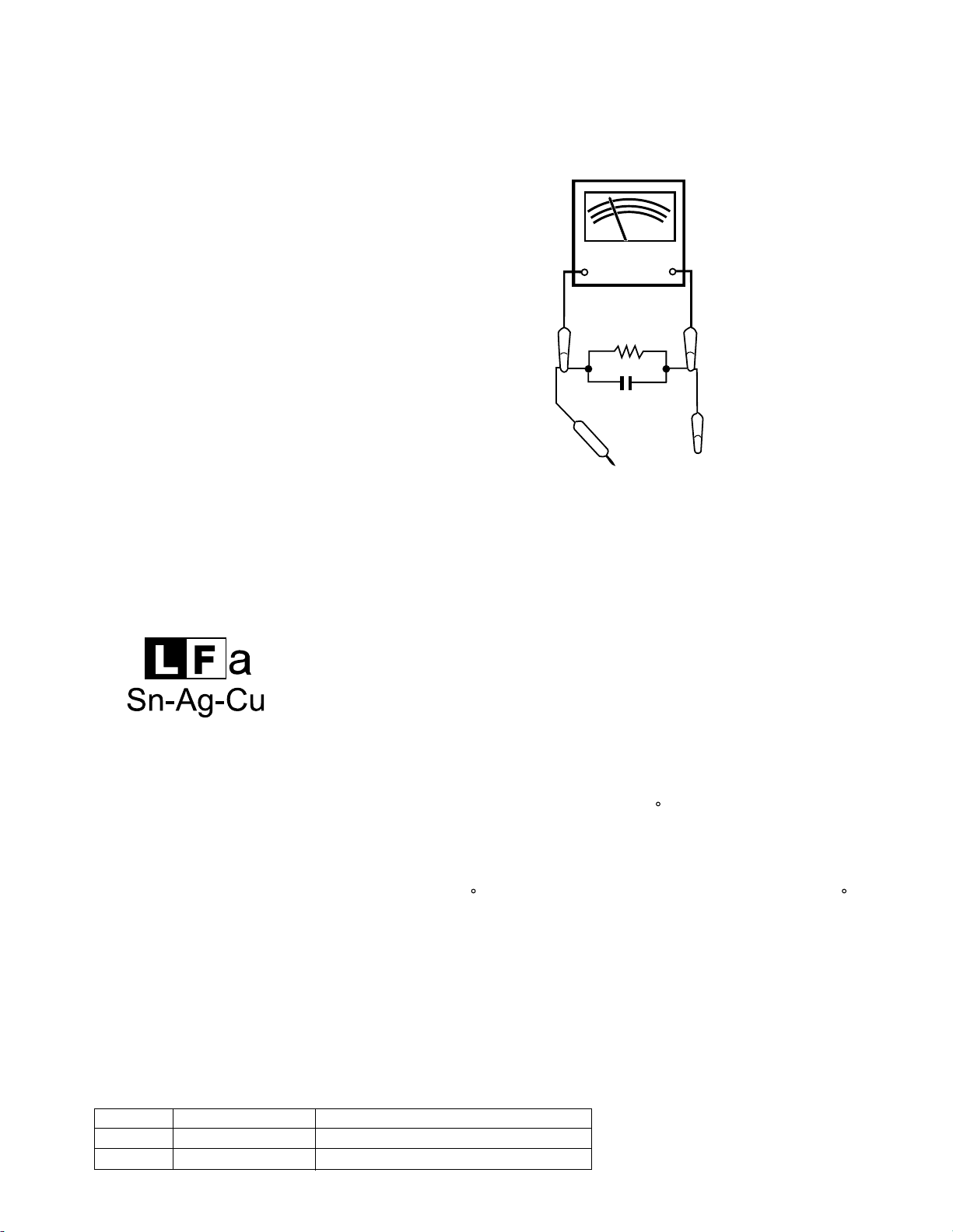
3. To be sure that no shock hazard exists, check for leakage current in
the following manner.
* Plug the AC line cord directly into a 120 volt AC outlet.
* Using two clip leads, connect a 1.5 kohm, 10 watt resistor paralleled
by a 0.15 µF capacitor in series with all exposed metal cabinet parts
and a known earth ground, such as conduit or electrical ground connected to earth ground.
* Use a VTVM or VOM with 1000 ohm per volt, or higher, sensitivity to
measure the AC voltage drop across the resistor (See diagram).
* Connect the resistor connection to all exposed metal parts having a
return path to the chassis (antenna, metal cabinet, screw heads,
knobs and control shafts, escutcheon, etc.) and measure the AC
voltage drop across the resistor.
All check must be repeated with the AC line cord plug connection
reversed.
Any reading of 0.3 volt RMS (this corresponds to 0.2 milliamp. AC.) or
more is excessive and indicates a potential shock hazard which must
be corrected before returning the audio product to the owner.
VTVM
AC SCALE
1.5 kohms
10 W
0.15 mF
TEST PROBE
TO EXPOSED
METAL PARTS
CONNECT TO
KNOWN EARTH
GROUND
1. Employing lead-free solder
"
Amp./Power1/Power2/Display/Main/LED/Switch/Headphones/Tuner
" of this model employs lead-free solder. The LF symbol indicates
lead-free solder, and is attached on the PWB and service manuals. The alphabetical character following LF shows the type of
lead-free solder.
Example:
Indicates lead-free solder of tin, silver and copper.
2. Using lead-free wire solder
When fixingthe PWBsoldered withthe lead-freesolder, apply lead-free wire solder. Repairing with conventional lead wire solder
may cause damage or accident due to cracks.
As the melting point of lead-free solder (Sn-Ag-Cu) is higher than the lead wire solder by 40 C, we recommend you to use a
dedicated soldering bit, if you are not familiar with how to obtain lead-free wire solder or soldering bit, contact our service station
or service branch in your area.
3. Soldering
As the melting point of lead-free solder (Sn-Ag-Cu) is about 220 C which is higher than the conventional lead solder by 40 C,
and as it has poor solder wettability, you may be apt to keep the soldering bit in contact with the PWB for extended period of
time. However, Since the land may be peeled off or the maximum heat-resistance temperature of parts may be exceeded,
remove the bit from the PWB as soon as you confirm the steady soldering condition.
Lead-free solder contains more tin, and the end of the soldering bit may be easily corrected. Make sure to turn on and off the
power of the bit as required.
If a different type of solder stays on the tip of the soldering bit, it is alloyed with lead-free solder. Clean the bit after every use
of it.
When the tip of the soldering bit is blackened during use, file it with steel wool or fine sandpaper.
Be careful when replacing parts with polarity indication on the PWB silk.
Lead-free wire solder for servicing
Ref No. DescriptionParts No.
PWB-A DUNTKV550SJ03 Amp./Power1/Power2
PWB-B DUNTKV549SJ03 Display/Main/LED/Switch/Headphones/Tuner
– i –
Page 3
AudioHT-X1Service ManualHT-X1MarketE
CHAPTER 1. GENERAL DESCRIPTION
[1] Specifications
FOR A COMPLETE DESCRIPTION OF THE OPERATION OF THIS UNIT, PLEASE REFER
TO THE OPERATION MANUAL.
HT-X1
Main unit
Dimensions Including the stand
Weight 4.9 lbs. (2.2 kg)
Frequency range FM: 87.5 - 108 MHz
Video output terminals Video output: RCA type 1
Audio output terminal Headphones: 16 - 50 ohms
Audio input terminals Audio input (AUX): RCA type 2
Other terminal System control 2
Signal system NTSC color
Supported disc types DVD (region number 1 or ALL),
Video signal Horizontal resolution: 500 lines
Audio
signal
Frequency
characteristics
S/N ratio CD:96dB(1kHz)
Dynamic
range
Total harmonic distortion ratio
CP-X1F
Type Full range system (magnetic shield)
Maximum input power 100 W
Rated input power 50 W
Impedance 4 ohms
Dimensions Width: 4-1/8" (105 mm)
Weight 2.0 lbs. (0.9 kg)/each
Width: 17" (430 mm)
Height: 7-5/8" (192 mm)
Depth: 4" (100 mm)
Excluding the stand
Width: 17" (430 mm)
Height: 6-3/4" (171 mm)
Depth: 3-1/2" (88 mm)
AM: 530 - 1,720 kHz
S-video output: S-terminal 1
Component video output: RCA type 3
(Y/PB/PR)
(recommended: 32 ohms)
Optical digital input: Square type 1
DVD-R/RW (video mode),
DVD+R/RW (video mode), audio CD,
CD-R, CD-RW
S/N ratio: 70 dB
Linear PCM DVD:
4 Hz to 22 kHz (sampling rate: 48 kHz)
4 Hz to 44 kHz (sampling rate: 96 kHz)
CD: 4 Hz to 20 kHz
Linear PCM DVD: 95 dB
CD: 94 dB
0.006 % maximum
3-1/8" (8 cm) speaker 1
Height: 8-1/8" (205 mm)
Depth: 4-1/8" (105 mm)
CP-X1C
Type Full range system (magnetic shield)
3-1/8" (8 cm) speaker 1
Maximum input power 100 W
Rated input power 50 W
Impedance 4 ohms
Dimensions Width: 7-1/4" (185 mm)
Weight 2.0 lbs. (0.9 kg)
Height: 4-7/8" (123 mm)
Depth: 4-1/2" (115 mm)
Subwoofer/amplifier unit
Amplifier:
Power source AC 120 V, 60 Hz
Power consumption 208 W
Dimensions Width: 7-7/8" (200 mm)
Weight 23.2 lbs. (10.5 kg)
Speaker terminals Front speakers, center speaker and
Other terminals System control 2
Power output (FTC) 50 watts minimum RMS per channel
Rated power output Front: 50 W + 50 W, Center: 50 W,
Subwoofer:
Type Bass reflex, 1 way system
Maximum input power 100 W
Rated input power 50 W
Impedance 4 ohms
Specifications for this model are subject to change without
prior notice.
Height: 15" (380 mm)
Depth: 17-1/2" (443 mm)
surround speakers: more than 4 ohms
into 4 ohms from 150 Hz to 20 kHz,
10% total harmonic distortion
Subwoofer:
50 watts minimum RMS into 4 ohms
from 20 Hz to 150 Hz, 10% total
harmonic distortion
Surround: 50 W + 50 W
(4 ohms at 1 kHz, 10 % T.H.D.)
Subwoofer: 50 W
(4 ohms at 100 Hz, 10 % T.H.D.)
6-1/2" (16 cm) woofer 1
HT-X1
CP-X1S
Type Full range system
3-1/8" (8 cm) speaker 1
Maximum input power 100 W
Rated input power 50 W
Impedance 4 ohms
Dimensions Width: 4-1/8" (105 mm)
Weight 1.7 lbs. (0.75 kg)/each
Height: 8-1/8" (205 mm)
Depth: 4-1/8" (105 mm)
1 – 1
Page 4
HT-X1
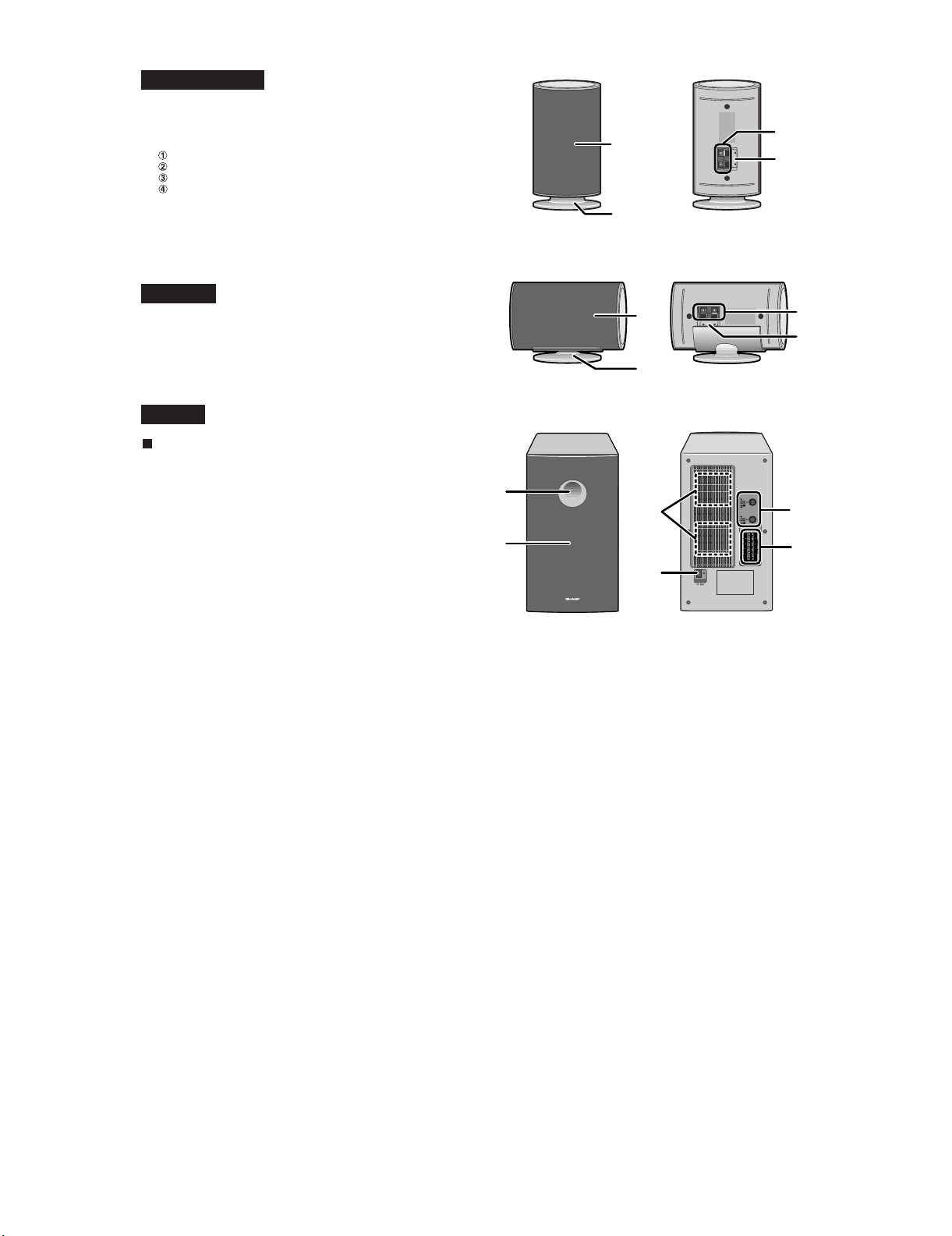
[2] Names of parts
HT-X1
Top and front panel
1. Disc Eject Button
2. Stop Button
3. Play Button
4. Chapter (Track) Skip Down or Fast Reverse Button
5. Chapter (Track) Skip Up or Fast Forward Button
6. Function Selector Button
7. Tuner (Band) Button
8. On/Stand-by Button
9. Disc Compartment
10. Main Unit Stand
11. Remote Sensor
12. Volume Control
13. Headphone Jack
Rear panel
1. FM 75 Ohm Antenna Jack
2. Antenna Ground Terminal
3. AM Antenna Terminal
4. Auxiliary (Audio Signal) Input Jacks
5. Component Video Output Jacks
6. S-video Output Jack
7. Video Output Jack
8. System Connection Jacks
(to subwoofer/amplifier unit)
9. Optical Digital Audio Input Jack
Removing the back cover of
the main unit:
For system connections, remove
the back cover first.
1 2 3 4 5 6 7 8
9
11
12
13
10
1
21 34 5 76 8 9
Display
11
Display
1. Program Indicator
2. Random Play Indicator
3. Repeat/One Track Repeat/A - B Repeat Indicators
4. 2 channel Stereo Sound Mode Indicator
5. Multi Channel Sound Mode Indicator
6. PCM Signal Indicator
7. DTS Signal Indicator
8. Dolby Digital Signal Indicator
9. Dolby Pro Logic Indicator
10. Audio Signal/Speaker Indicators
11. Track Indicator
12. Chapter Indicator
13. Title Indicator
14. Pause Indicator
15. Play Indicator
16. Total Indicator
17. Angle Indicator
18. FM Stereo Mode Indicator
19. FM Stereo Receiving Indicator
20. Sleep Indicator
2
1
2
3
4
5
6
7
8
9
10
11
12
13
14
15
16
17
18 19 20
1 – 2
Page 5
HT-X1
HT-X1
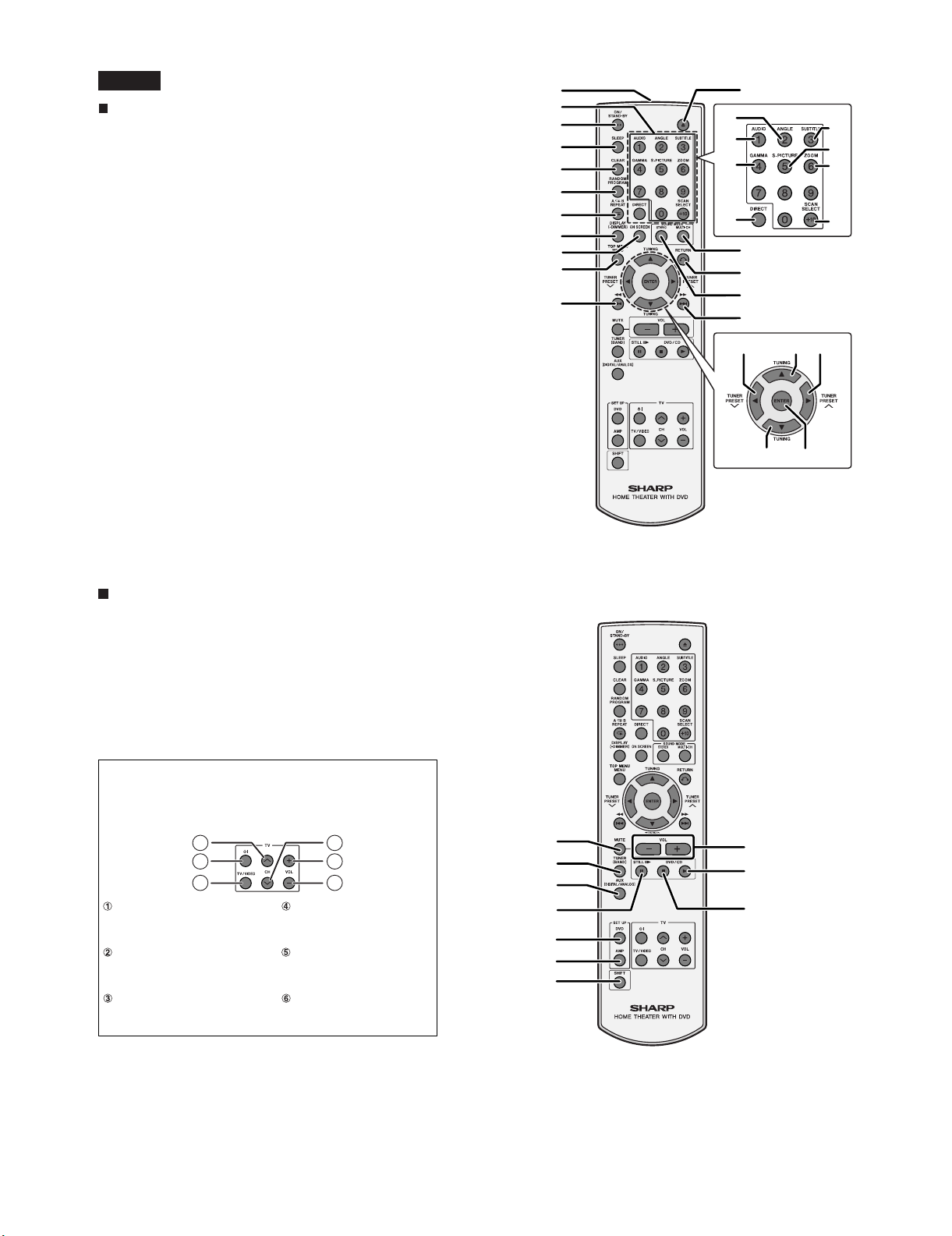
Remote control
1. Remote Control Transmitter
2. Direct Number Buttons
3. On/Stand-by Button
4. Sleep Button
5. Clear Button
6. Random or Program Button
7.A-BRepeat or Repeat Button
8. Unit Display Select or Dimmer Button
9. On Screen Display On/Off Button
10. Top Menu or Menu Button
11. Chapter (Track) Skip Down or Fast Reverse Button
12. Disc Eject Button
13. Multi Channel Select Button
14. Return Button
15. Stereo (2 channel) Select Button
16. Chapter (Track) Skip Up or Fast Forward Button
17. Angle Button
18. DVD Audio Language Select or
CD Audio Output Select Button
19. Gamma Button
20. Direct Button
21. Subtitle Button
22. Super Picture Button
23. Zoom Button
24. Progressive Scan Mode Select Button
25. Tuner Preset Down or Cursor Button
26. Tuning Up or Cursor Button
27. Tuner Preset Up or Cursor Button
28. Tuning Down or Cursor Button
29. Enter Button
10
11
1
2
3
4
5
17
18
19
12
21
22
23
6
7
20
24
8
9
13
14
15
16
27
2625
28 29
Remote control
1. Mute Button
2. Tuner (Band) Button
3. Auxiliary Button
4. Frame Advance or Pause Button
5. DVD Initial Setting Button
6. Amplifier Initial Setting Button
7. Shift Button
8. Volume Up and Down Buttons
9. Play Button
10. Stop Button
TV Operation Buttons
You can operate some functions of SHARP's TVs with the remote
control of this system.
However, some models cannot be operated.
1
2
3
TV Channel Up Button TV Channel Down Button
Switches the TV channel up. Switches the TV channel
TV On/Stand-by Button TV Volume Up Button
Sets the TV power to"ON" or
"STAND-BY".
TV/VCR Input SelectButton
Switches the input to TV or
VCR.
4
5
6
down.
Turns up the TV volume.
TV Volume Down Button
Turns down the TV volume.
1
2
8
9
3
4
10
5
6
7
1 – 3
Page 6
HT-X1
CP-X1F/CP-X1S
1. Speaker
2. Speaker Stand
3. Speaker Terminals
4. Color Label
White ... Left Front Speaker
Red ... Right Front Speaker
Blue ... Left Surround Speaker
Gray ... Right Surround Speaker
CP-X1C
1. Speaker
2. Speaker Stand
3. Speaker Terminals
4. Color Label: Green
HT-X1
Subwoofer/amplifier unit
1. Bass Reflex Duct
2. Woofer
3. Cooling Fan
4. AC Power Input Jack
5. System Connection Jacks (to main unit)
6. Speaker Terminals
1
3
4
2
1
3
4
2
1
3
2
5
6
4
1 – 4
Page 7

AudioHT-X1Service ManualHT-X1MarketE
CHAPTER 2. ADJUSTMENTS
[1] TEST Mode
1. TUNER TEST (Tuner button + Stop button + Power
button)
HT-X1
5. SLOT-IN MECHA TEST (“EJECT button” + “FUNCTION button” + “POWER button”)
VFD DISPLAY TEST CYCLE NUMBER
DISC LOAD ERROR: “EL xx” (xx MEANS TEST CYCLE NUMBER)
DISC EJECT ERROR: “EE xx” (xx MEANS TEST CYCLE NUMBER)
First, the ALL_MUTE_OFF_TEST key code is sent to AMP to start it up
with all mute controls disabled.
1.1. INITIAL SETTINGS:
VOLUME = 20
FUNCTION = FM ST 87.50MHz (P-01)
1.2. PRESET STATIONS:
P-01: FM ST 87.50 MHz
P-02: FM ST 108.00 MHz
P-03: FM ST 98.00 MHz
P-04: FM ST 90.00 MHz
P-05: FM ST 106.00 MHz
P-06: AM 522 KHz
P-07: AM 1620 KHz
P-08: AM 990 KHz
P-09: AM 603 KHz
P-10: AM 1404 Hz
P-36: FM MONO 106.00 MHz
P-37: FM MONO 90.00 MHz
P-38: FM MONO 98.00 MHz
P-39: FM MONO 108.00 MHz
P-40: FM MONO 87.50 MHz
1.3. WHEN SYSTEM ENTER TUNER TEST MODE, BELOW
FOUR BUTTONS ON MAIN UNIT WILL CHANGE TO OTHER
FUNCTIONS TEMPORARILY
“STOP” BUTTON: TUNING DOW
“PLAY” BUTTON: TUNING UP
“SKIP DOWN” BUTTON: TUNER PRESET DOWN
“SKIP UP” BUTTON: TUNER PRESET UP
6. DVD RESTORE (“PLAY button” + “FUNCTION button” + “POWER button”)
DVD SETUP SETTINGS RESTORED
AMP SETUP SETTINGS RESTORED
SOUND MODE SETTINGS RESTORED
ERRASE ALL OF CONTENTS OF PROGRAM PLAYBACK LIST
SHOW DVD ROM DATA VERSION NUMBER ON BOTH VFD AND
MONITOR
7. SYSTEM RESTORE (“STOP” button + “FUNCTION” button + “POWER” button)
ERRASE ALL OF CONTENTS OF TUNER MEMORY
RESET TUNER PRESET FLAG
SET INITIAL VOLUME TO 20
SET INITIAL FUNCTION TO DVD/CD
SET FM ST FREQUENCY TO 87.50MHz
SET FM MONO FREQUENCY TO 87.50MHz
SET AM FREQUENCY TO 522KHz
SHOW SYSTEM SOFTWARE VERSION ON VFD
2. VOLUME TEST (SKIP Down button + STOP button
+ POWER button)
2.1. INITIAL SETTINGS:
VOLUME = 23
FUNCTION = AUX DIGITAL
FM ST FREQUENCY = 87.50MHz
FM MONO FREQUENCY = 87.50MHz
AM FREQUENCY = 522KHz
VOLUME 0 >> VOLUME 1 >> VOLUME 23 >> VOLUME 40 >> VOLUME MAX
3. KEY TEST (SKIP Up button + PLAY button +
POWER button)
3.1. PRESS EACH BUTTON OF MAIN UNIT EXCEPT “ON/
STAND-BY” BUTTON, AND THEN PRESS “ON/STAND-BY”
BUTTON.
KEY OK: “OK” SHOWN ON VFD
KEY NG: “ERROR”SHOWN ON VFD
4. VFD TEST (“SKIP Up button” + “STOP button” +
“POWER button”)
BACK LIGHT LED = ON
USE “SKIP UP” BUTTON TO CHANGE VFD DISPLAY MODE AND
BACK LIGHT LED MODE
2 – 1
Page 8
HT-X1
AudioHT-X1Service ManualHT-X1MarketE
CHAPTER 3. MECHANISM BLOCKS
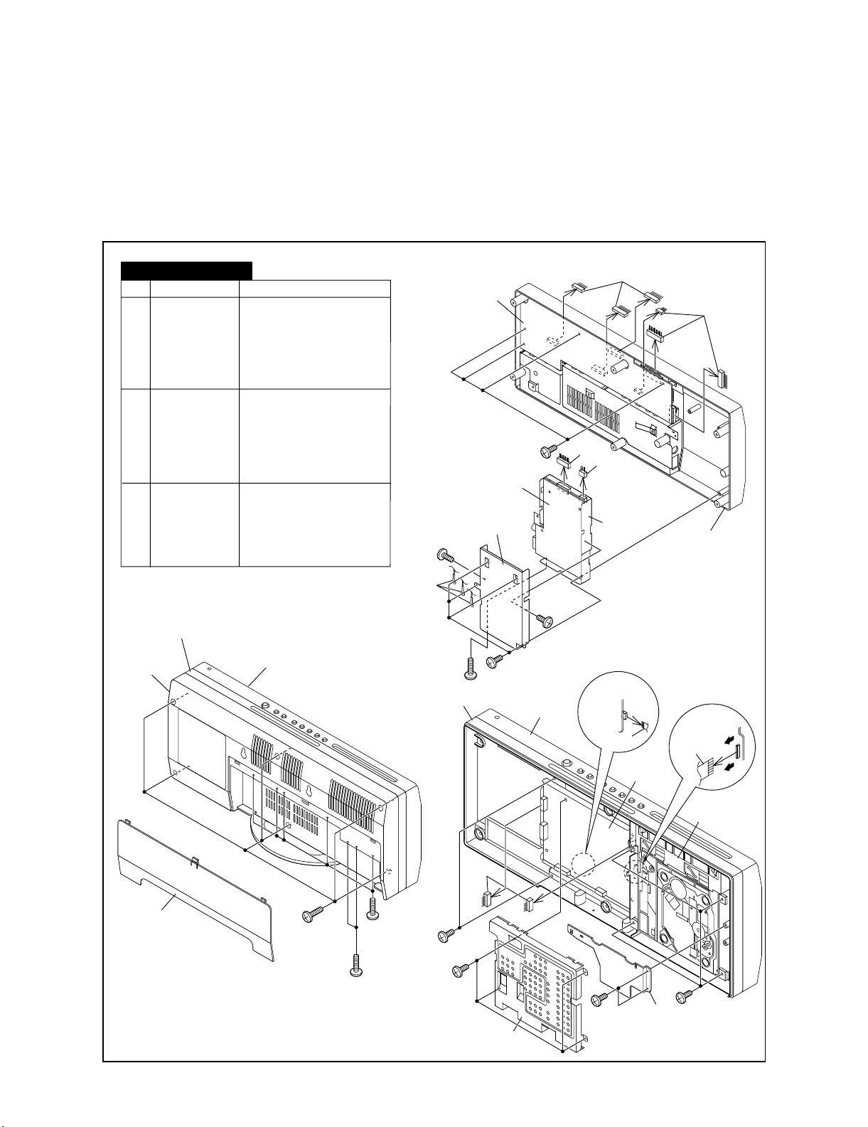
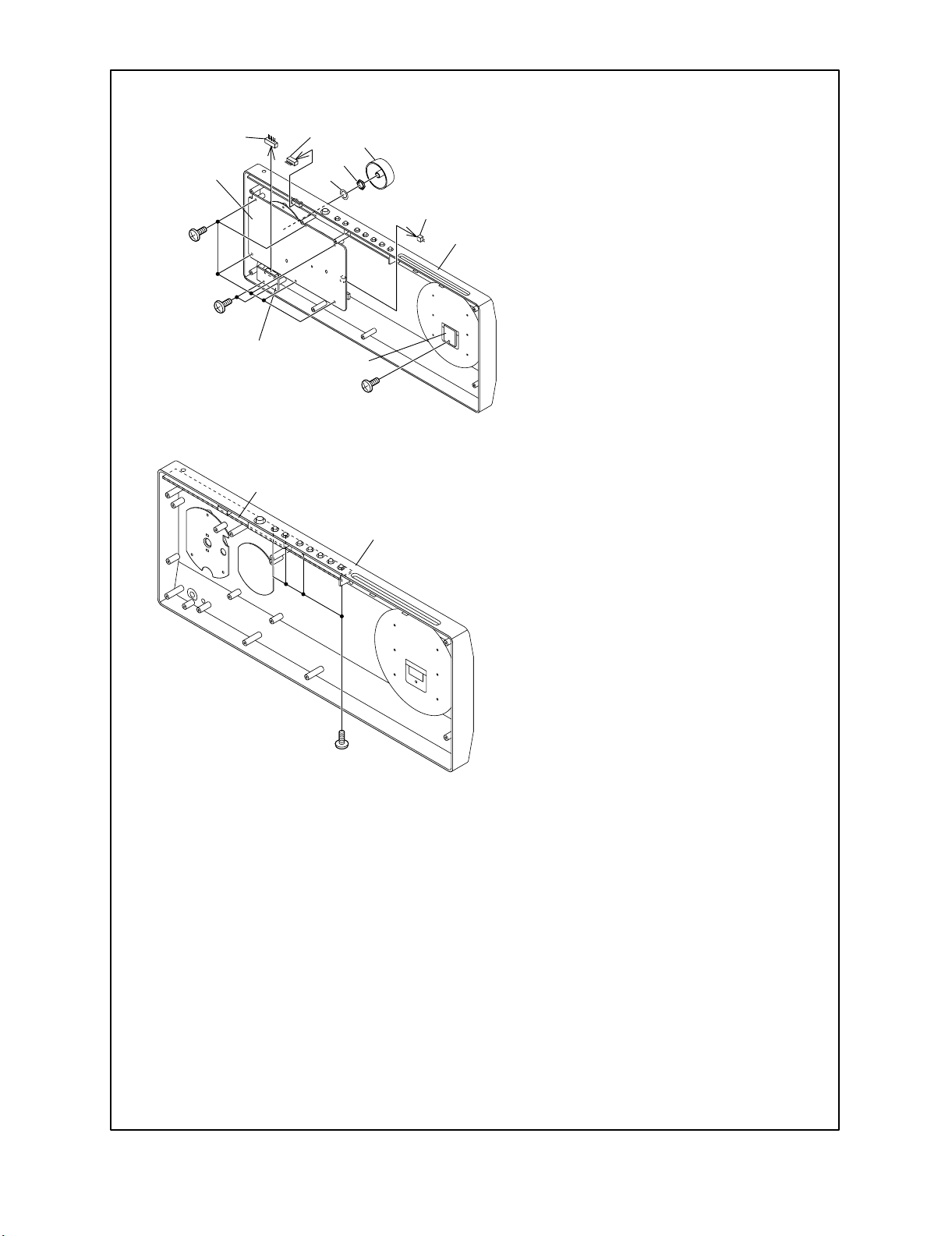
[1] Caution on diassembly
Caution on Disassembly
Follow the below-mentioned notes when disassembling the unit and reassembling it, to keep it safe and ensure excellent performance:
1. Take cassette tape, and compact disc out of the unit.
2. Be sure to remove the power supply plug from the wall outlet before starting to disassemble the unit.
3. Take off nylon bands or wire holders where they need to be removed when disassembling the unit. After servicing the unit, be sure to rearrange
the leads where they were before disassembling.
HT-X1 (DVD Unit)
STEP
Rear Panel
REMOVAL PROCEDURE
1 Rear Panel with 1. Terminal Cover ....... (A1) x1
PWB
Center Panel with
2
DVD Servo PWB/
DVD Mechanism
Unit
3 Front Panel with
Display/
Headphone/
Switch/LED PWB
Center Panel
2. Screw .................... (A2) x6Main/Tuner
3. Socket ..................... (A3) x7
4. Screw ................... (A4) x15
5. Socket ......................(A5) x1
6. Screw ...................... (A6) x3
7. Shield Box A ........... (A7) x1
8. Shield Box B ........... (A8) x1
1. Screw ...................... (B1) x2
2. Screw
3. Shield ...................... (B3) x1
4. Flat Cable ............... (B4) x2
5. Socket ..................... (B5) x2
6. Screw ...................... (B6) x2
7. Pickup Cover............(B7) x1
8. Screw ...................... (B8) x4
1. Knob ...................... (C 1) x1
2. Nut .......................... (C2) x1
3. Screw ...................... (C3) x6
4. Socket ..................... (C4) x3
5. Screw ...................... (C5) x2
6. Screw ...................... (C6) x4
7. Screw ...................... (C7) x1
......................(B2) x4
Front Panel
Lug Wire
(A6)x1
M2x3mm
Main PWB
Tuner PWB
(A6)x1
M2x3mm
Center Panel
(A4)x4
M3x10mm
(A7)x1
(A4)x4
M3x10mm
(A6)x1
M2x3mm
Front Panel
(A3)x1
(A5)x1
(A8)x1
Display PWB
(A3)x3
(B4)x1
DVD Servo
PWB
(A3)x3
Rear Panel
DVD Servo
PWB
(B4)x1
Pull
Pull
(A1)x1
(A2)x6
M3x12mm
(A4)x5
M3x6mm
(A4)x2
M2.5x10mm
(B1)x2
M3x10mm
(B2)x4
M3x8mm
3 – 1
(B5)x2
(B3)x1
(B6)x2
M2.5x10mm
(B7)x1
DVD Mechanism
Unit
(B8)x4
M3x8mm
Page 9
HT-X1
(C4)x1
Display PWB
(C3)x6
M2.5x8mm
(C5)x2
M2.5x8mm
Headphone PWB
Switch PWB
(C4)x1
(C2)x1
Washer
LED PWB
(C1)x1
(C4)x1
Front Panel
(C7)x1
M3x6mm
Front Panel
(C6)x4
M2.5x8mm
3 – 2
Page 10
HT-X1
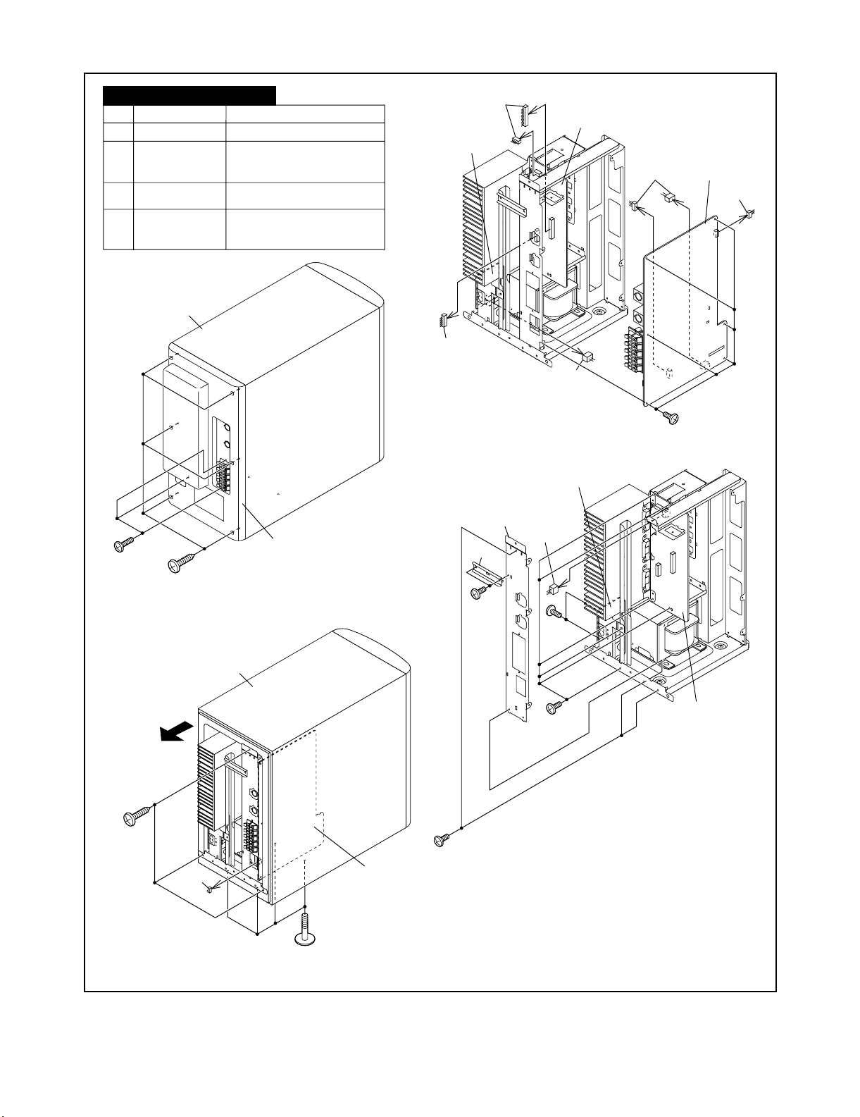
HT-X1 (Subwoofer Unit)
STEP
REMOVAL PROCEDURE
1 Rear Cabinet 1. Screw ...................... (A1) x9
Amp. Unit
2 1. Screw ...................... (B1) x7
2. Socket
3.
3 Power1 PWB
4 Amp./Power2
PWB
Subwoofer Box
1. Screw ...................... (C1) x6
2. Socke t ...................... (C2) x7
1. Screw .................... (D1) x13
2. Bracket ................... (D2) x2
3. Socke t ..................... (D3) x1
.................... (B2) x1
It pulls out to the front.
(C2)x2
Powe r2 P WB
(C2)x1
Amp. PWB
(C2 )x1
Power2 PWB
(C2)x2
Powe r1 P WB
(C2 )x1
(C1)x6
M3x6mm
(A1)x3
M3x12mm
(B1)x3
M4x16mm
(A1)x6
M4x16mm
Suboofer Box
(B2)x1
Rear Cabinet
Powe r1 P WB
(D2)x1
(D1)x2
M3x6mm
(D1)x3
M3x6mm
(D2)x1
(D3)x1
(D1)x2
M3x6mm
(D1)x6
M3x6mm
Amp. PWB
(B1)x4
M4x28mm
3 – 3
Page 11

—— MEMO ——
HT-X1
3 – 4
Page 12
HT-X1
AudioHT-X1Service ManualHT-X1MarketE
CHAPTER 4. DIAGRAMS
[1] Block diagram
FROM
POWER1 PWB
CNS402A
CNS402B
FROM
POWER1 PWB
Q102
CNP402A
CNP402B
Q101
IC101
POWER AMP.
LM4732TA
D102
C/SW
Q103
IC104
BUFFER
AMP.
8
IC104
NJM4558D
1
Figure 4-1 BLOCK DIAGRAM (1/8)
5
7
6
4
2
3
ZD101
ZD102
CNP202
D101
F102
6.3A/125V
CNS202
FROM
MAIN POWER TRANSFORMER
F101
6.3A/125V
4 – 1
Page 13
HT-X1
F101
R
IC102
POWER AMP.
LM4732TA
FL/FR
CNP401
CNS401
6.3A/125V
IC103
POWER AMP.
LM4732TA
FROM
POWER1 PWB
SL/SR
MER
Figure 4-2 BLOCK DIAGRAM (2/8)
4 – 2
Page 14
HT-X1
0
G
2
0
4 3 2 1
IC404
NJM4558D
5 6 7 8
IC404
BUFFER
TO
CNP402
AMP.PWB
BI402
Q403
Q404
D453
D452
D454
D455
TO
CNP401
AMP.PWB
2345678910
1
BI401
D432
Q447
D433
MAIN PWB
S101A
Q446
4 3 2 1
IC405
IC405
NJM4558D
BUFFER
5 6 7 8
S101B
1
2
3
4
TO
5
6
7
8
9
10
11
12
13
Q453
4 3 2 1
IC406
IC406
BUFFER
NJM4558D
5 6 7 8
Q451
3
Q452
ZD424
2
1
Q450
Q407
Q408
Q409
Q412
Q456
Q454
Q459
D440
D441
D442
D443
D457
D456
D458
D459
Q455
Q458
Q457
Q443
D435
Q435
ZD423
RLY401
RLY402
D426
Q448
D434
D425
Q434
D42
Q429
MAIN PWB
S101A
D410
S102B
1
2
3
4
5
TO
6
7
8
9
10
11
12
13
171615 1413 121110
IC407
TCD4094B
1 2 3 4 5 6 7 8
Q413
Q414
3
IC2
2
IC203
AN78L
VOLTAGE RE
1
2
3
D216
Figure 4-3 BLOCK DIAGRAM (3/8)
4 – 3
Page 15
TO
CNP401
AMP.PWB
2345678910
1
Q446
Q443
D435
Q435
ZD423
HT-X1
BI401
Q439
D432
Q447
D433
RLY401
RLY402
D426
Q448
D434
D425
Q434
D422
Q432
Q433
1
3
3
2
1
RLY403
D424
1N4004
Q430
Q429
Q437
2
Q437A
D429
Q444
D420
D416
D417
D419
ZD425
D427
Q436
Q436A
D427A
D411
D421
D418
Q438
Q438A
D436
D437
D431
Q445
Q415
Q416
CNP205
1
1
M
2
3
Q439A
M401
2
M
3
M402
BI205
+
+
-
-
+
+
-
-
+
+
-
-
+
+
-
-
+
+
-
-
SO401
CNP206
Q413
321
IC
2
321
IC201
D209
REGULATOR
IC203
AN78L05
VOLTAGE REGULATOR
1
2
3
D216
IC201
KIA7805API
VOLTAGE
D217
D219
KIA7812API
VOLTAGE
R
E
G
ULATOR
D218
D220
02
T202
SUB POWER
TRANSFORMER
D205
D206
D207
D208
D210
ZD202
ZD201
Q201
Q203
D211
D221
RLY400
BI203
D212
CNP203
CNP204
LF201
LINE FILTER
F201
2A/125V
AMP PWB
CNS202
TO
CNS204
S0202
AC SOCKET
T201
POWER TRANSFORMER
CNP201
CNS202
CNS201
AC POWER
SUPPLY CORD
AC 120 V,
60 Hz
Figure 4-4 BLOCK DIAGRAM (4/8)
4 – 4
Page 16
HT-X1
E
D701
BI301
TO
TUNER PWB
CNW703
D706
IC701
0058SJ
TO
PWB
DVD SERVO
CNW704
TO
MAIN PWB
CNW702
L704
SYSTEM MICROCOMPUT
X701
X702
L702
TO
MAIN PWB
D708
Q702
D706A
SW700
D706B
JOG VOLUME
CFW9
D707
LED702
1N4148
LPBB73V1
CNW707
Q701
CNP707
Figure 4-5 BLOCK DIAGRAM (5/8)
4 – 5
Page 17
VFD701
FL DISPLAY
CNW705
CNP705
HT-X1
L706
CFW6
RX701
GP1UD261
321
MPUTER
SW708
SW704 SW707
Q506
SW706
SW705
RX702
GP1UD261
21
Q507
3
CNP706
FROM
DVD MECHIANISM
Q508
Q509
SW703
SW702
SW701
CNW609
CNP609
D703
D702
L703
L701
L705
D704
Q709
Q703
D705
ZD701
Q704
Q505
Q510
CFW9
B
Figure 4-6 BLOCK DIAGRAM (6/8)
4 – 6
Page 18
HT-X1
IC509
NJM14558
IC501
KIA7812API
IC503
LM2576T
D508
1
3
2
L501
Q502
D509
Q501
TO
DVD SERVO PWB
TO
POWER1 PWB
TO
POWER1 PWB
BI501
S101A
1
2
3
4
5
6
7
8
9
10
11
12
13
S102A
1
2
3
4
5
6
7
8
9
10
11
12
13
1
2
KIA7805API
D505
VREF
CL
VDD
VSS
CE
DI
3
LOUT
ROUT
D506
IC502
RBS
LBS
IC505
LC75341M
RTRE
RSL0
RIN
R4R3R2
LTRE
LSL0
LIN
L4
R1
L1L2L3
D507
IC508
NJM14558
IC406
NJM14558
NC
CNW302
FROM
TUNER PWB
IC507
CD4053M
IC504
NJM4558D
CNP702
L502
AUX L
IC512
NJM4558D
CNW508A
CNW508B
Figure 4-7 BLOCK DIAGRAM (7/8)
4 – 7
FROM
DISPLAY PWB
Page 19
HT-X1
9
FROM
DVD SERVO PWB
L5A1
123
IC511
KIA7805API
CFW5
TUN L
BI502
CNP704
FROM
DISPLAY PWB
CE
DI
CL
Q518
Q517
Q504
Q503
IC510
NJM4558D
Q5A3
Q5A4
BI503
BI506
10
9
8
7
6
5
4
3
2
1
TO
DVD SERVO PWB
TO
DVD SERVO PWB
TUN R
S503
L513B
L513A
L503
Q521
Q522
2 1
3
S501
D512
D511
S504
L506
L507
L508
D504
D503
S505
COMPONENT
VIDEO OUT
Figure 4-8 BLOCK DIAGRAM (8/8)
4 – 8
Page 20
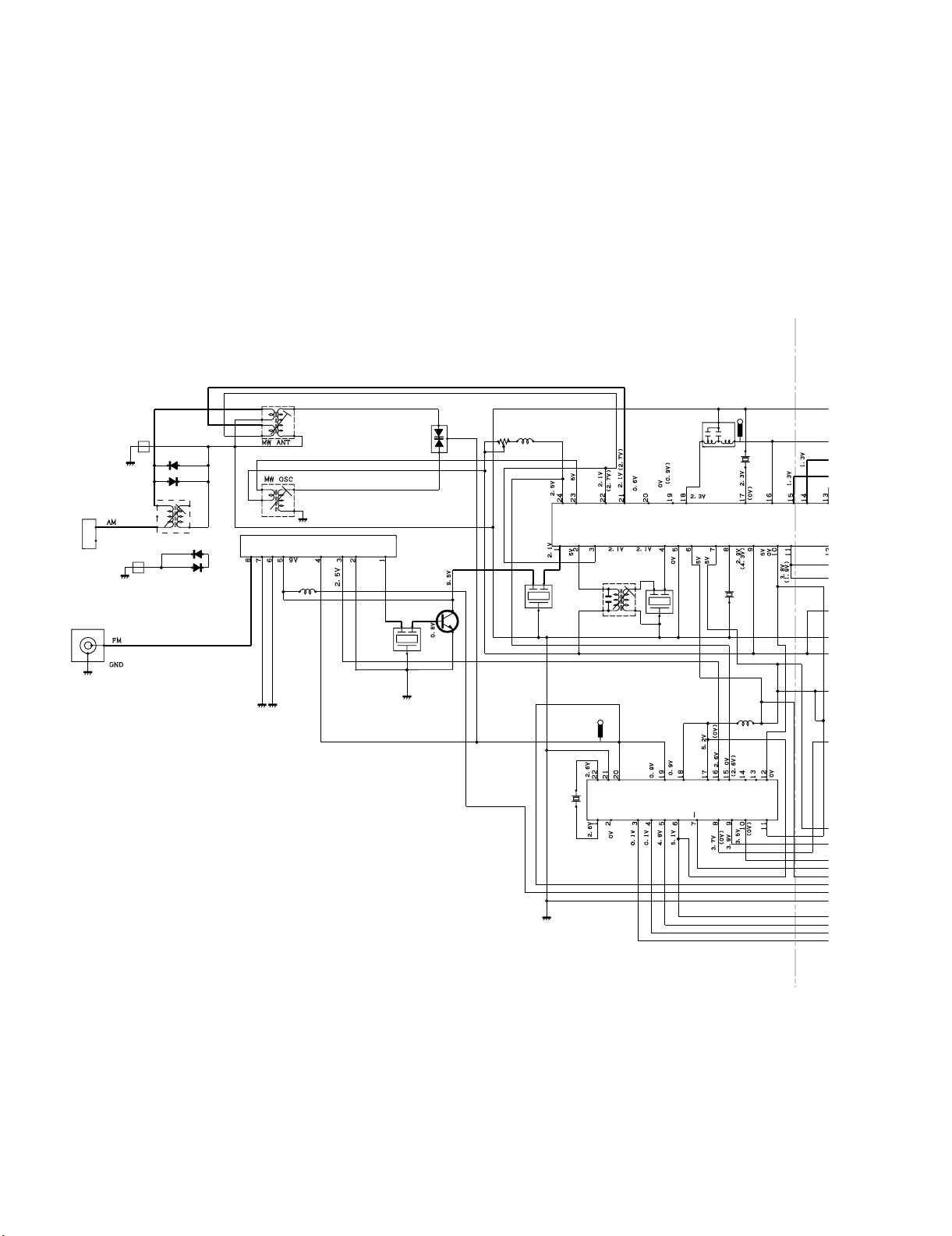
HT-X1
PHASE
MO/ST
AM ANTENNA
TERMINAL
FM ANTENNA
SO302
TERMINAL
SO301
D301
D302
L301
D303
D304
1N4148
1N4148
1N4148
1N4148
T302
T306
L342
IC301
VD301
SVC348S
IC301
NSA003SJ
FM FRONT END
CF303
Q301
FM IF DET. /FM MPX./AM IF
VR351
L353
1mH
IN
IN
OUT
AM OSC
IN
AM MIX
FM IF
CF302
2SC380 O
X352
4.5 MHz
AM RF
AM OSC
FM AFC
IC303
OUT
LA1832S
REG
T351
AM IF
VSS
IC302
AOUT
XOUTXIN
LC72131
CEDICL
NC
IC303
L354
X351
456 KHz
OUT
OUT
VSM
CUT
FM/AM
AM IF
IN
CF352
AIN
AM LOW
GND
SD
PD
DO
VDD
STEREO
CF351
FM IN
MPX VCO
FM DET
L351
100uH
NC
AM IN
FMFMMUTE
MO/ST
OUT
R-CH
L-CH
MPX IN
VCC
PHASE
IF OUT
NC
FIN
I
IF REQ
Figure 4-9 BLOCK DIAGRAM (8/10)
4 – 9
IC302
TUNER
(PLL)
Page 21
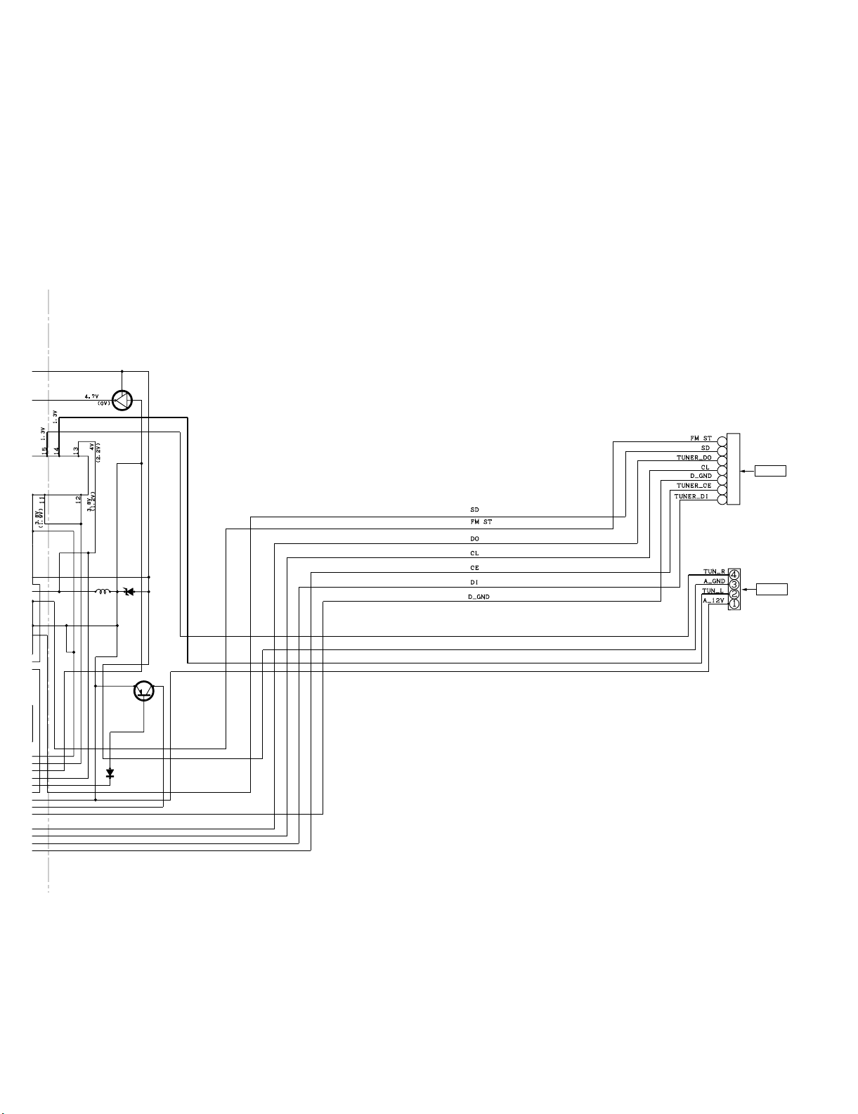
IF OUT
R-CH
PHASE
HT-X1
Q351
KRC104 M
1
2
3
CNP302
7
P6-7 1-D
6
FROM
DISPLAY PWB
OUT
OUT
L-CH
MO/ST
(AM/FM)
PHASE
5
4
CNS302
3
2
1
L352
100uH
KTA1266 GR
D308
1N4148
Q360
11.7V
DZH05C2
10.9V
ZD351
10.8V
+B+B
CNP301
P6-5 4-F
FROM
MAIN PWB
CNW301
Figure 4-10 BLOCK DIAGRAM (8/10)
4 – 10
Page 22
HT-X1
AudioHT-X1Service ManualHT-X1MarketE
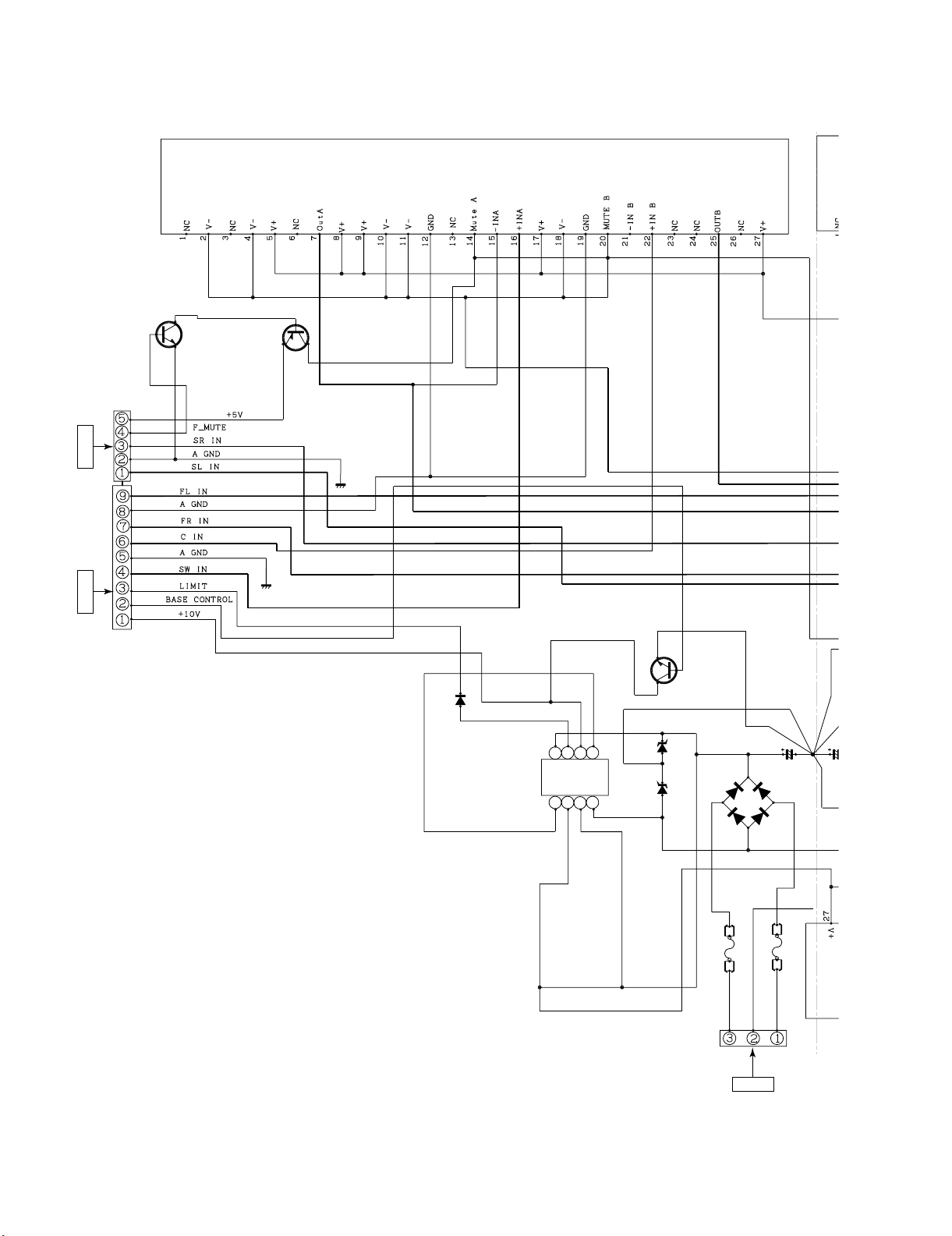
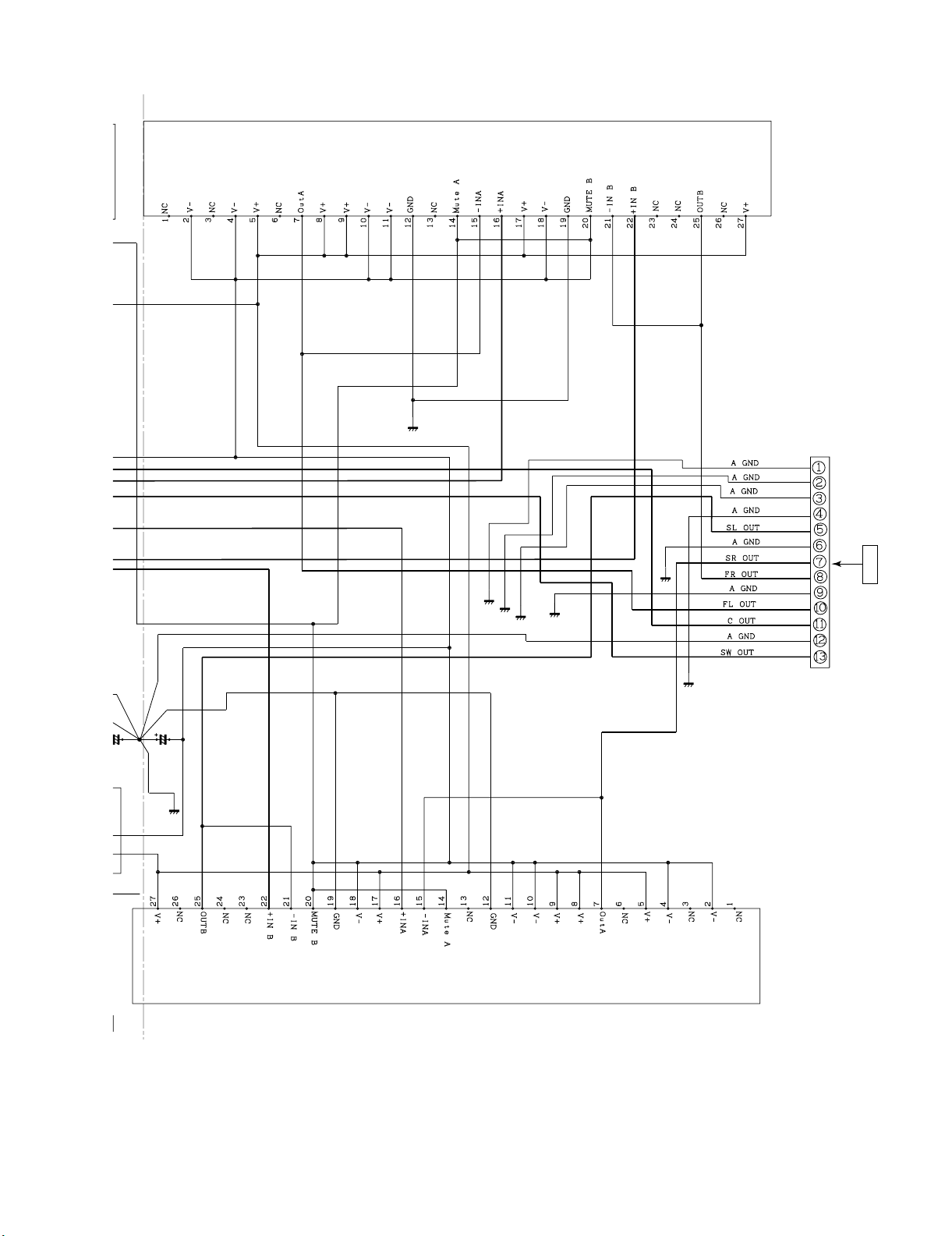
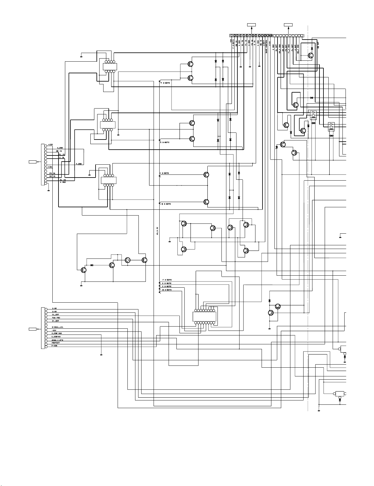
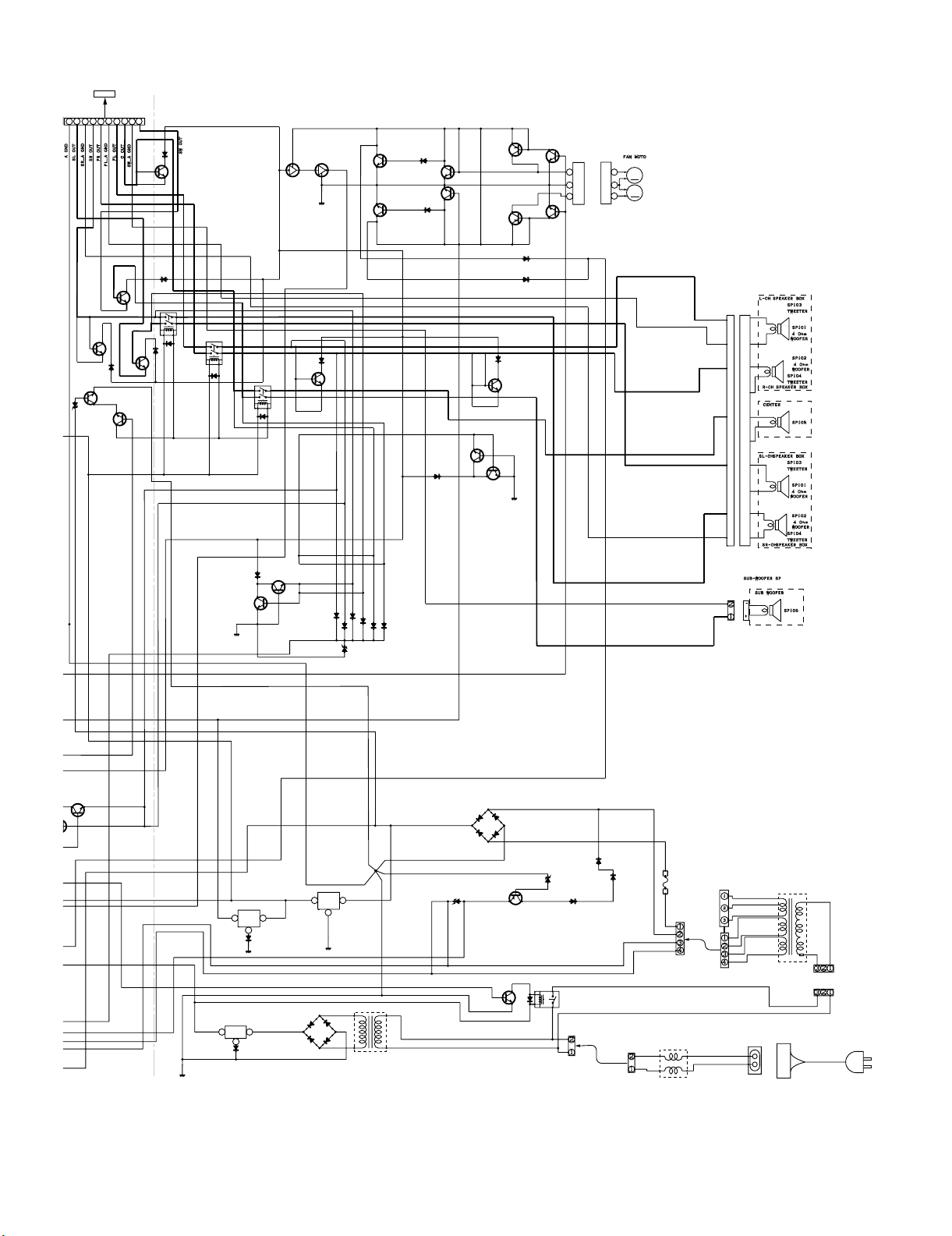
CHAPTER 5. CIRCUIT DESCRIPTION
[1] Notes on schematic diagram
•Resistor:
To differentiate the units of resistors, such symbol as K and M are
used: the symbol K means 1000 ohm and the symbol M means
1000 kohm and the resistor without any symbol is ohm-type resistor. Besides, the one with “Fusible” is a fuse type.
• Capacitor:
To indicate the unit of capacitor, a symbol P is used: this symbol P
means pico-farad and the unit of the capacitor without such a symbol is microfarad. As to electrolytic capacitor, the expression
“capacitance/withstand voltage” is used.
(CH), (TH), (RH), (UJ): Temperature compensation
(ML): Mylar type
(P.P.): Polypropylene type
• Schematic diagram and Wiring Side of P.W.Board for this model are
subject to change for improvement without prior notice.
REF. NO DESCRIPTION POSITION
SW700 JOG VOLUME ON—OFF
SW701 POWER ON—OFF
SW702 PLAY ON—OFF
SW703 STOP ON—OFF
[2] Types of transistor
• The indicated voltage in each section is the one measured by Digital Multimeter between such a section and the chassis with no signal given.
1. In the tuner section,
indicates AM
indicates FM stereo
2. In the CD section, the CD is stopped.
• Parts marked with “ “ ( ) are important for maintaining the safety of the set. Be sure to replace these parts with
specified ones for maintaining the safety and performance of the
set.
REF. NO DESCRIPTION POSITION
SW704 EJECT ON—OFF
SW705 TUNER ON—OFF
SW706 FUNCTION ON—OFF
SW707 PRESET UP ON—OFF
SW708 PRESET DOWN ON—OFF
FRONT
VIEW
ECB
(S)(G)(D)
(1)(2)(3)
2HC1815 GR
2SC535 C
2SC380 O
KRC104 M
KTA1266 GR
KTA1271 Y
KRA107 M
KRC107 M
KTC3199 GR
KTC3200 GR
KTC3203 Y
2SB561 C
2SB562 C
B
(3)
E
(1)
TOP
VIEW
2SD601 AR
C
(2)
5 – 1
Page 23
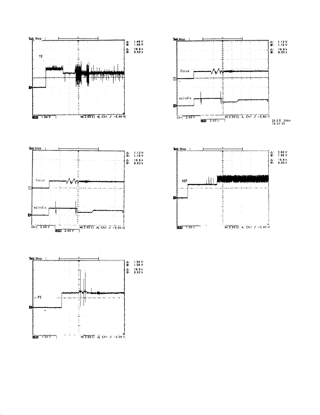
[3] Waveforms of circuit
HT-X1
5 – 2
Page 24
HT-X1
[4] Voltage
PIN
NO.
10
11
12
13
14
15
16
17
18
19
20
21
22
23
24
25
26
27
PIN
NO.
10
11
12
13
14
15
16
17
18
19
20
21
22
23
24
25
26
27
PIN
NO.
10
11
12
13
14
15
16
17
18
19
20
21
22
23
24
25
26
27
1
2
3
4
5
6
7
8
9
1
2
3
4
5
6
7
8
9
1
2
3
4
5
6
7
8
9
IC101
VOLTAGE
30.59 V
30.55 V
30.59 V
-30.55 V
30.59 V
30.59 V
30.6 V
-30.6 V
-30.6 V
-3.33 V
30.59 V
-30.6 V
-3.33 V
30.59 V
IC102
VOLTAGE
30.59 V
30.55 V
30.59 V
-30.55 V
30.59 V
30.59 V
30.6 V
-30.6 V
-30.6 V
-3.33 V
30.59 V
-30.6 V
-3.33 V
30.59 V
IC103
VOLTAGE
30.59 V
30.55 V
30.59 V
-30.55 V
30.59 V
30.59 V
30.6 V
-30.6 V
-30.6 V
-3.33 V
30.59 V
-30.6 V
-3.33 V
30.59 V
PIN
NO.
PIN
NO.
PIN
NO.
PIN
NO.
PIN
NO.
10
11
12
13
14
15
16
17
18
19
20
21
22
PIN
NO.
10
11
12
13
14
15
16
17
18
19
20
21
22
23
24
1
2
3
4
5
6
7
8
1
2
3
1
2
3
1
2
3
1
2
3
4
5
6
7
8
9
1
2
3
4
5
6
7
8
9
IC104
VOLTAGE
-8.57 V
2.77 V
1.02 V
-9.94 V
-8.56 V
3.86 V
-8.61 V
10.04 V
IC201
VOLTAGE
11.7 V
0.62 V
5.58 V
IC202
VOLTAGE
19.8 V
0V
11.99 V
IC203
VOLTAGE
5.7 V
10.36 V
0.59 V
IC302
VOLTAGE
1.85 V
4.23 V
11.01 V
2.67 V
2.57V
1.16 V
2.3 V
2.31 V
4.06 V
0.72 V
0.72 V
2.25 V
1.79 V
IC303
VOLTAGE
1.86 V
3.77 V
1.85 V
1.86 V
1.71 V
1.08 V
4.46 V
2.22 V
4.23 V
3.87 V
2.5 V
2.89 V
2.28 V
3.77 V
2.27 V
2.27 V
1.25 V
1.31 V
1.98 V
1.65 V
1.84 V
1.85 V
0.99 V
2.76 V
PIN
NO.
PIN
NO.
PIN
NO.
PIN
NO.
10
11
12
13
14
15
16
PIN
NO.
PIN
NO.
PIN
NO.
1
2
3
4
5
6
7
8
1
2
3
4
5
6
7
8
1
2
3
4
5
6
7
8
1
2
3
4
5
6
7
8
9
1
2
3
1
2
3
1
2
3
IC404
VOLTAGE
5.43 V
5.41 V
5.43 V
0V
5.43 V
5.43 V
5.42 V
10.83 V
IC405
VOLTAGE
5.43 V
5.41 V
5.43 V
0V
5.43 V
5.43 V
5.42 V
10.83 V
IC406
VOLTAGE
5.43 V
5.41 V
5.43 V
0V
5.43 V
5.43 V
5.42 V
10.83 V
IC407
VOLTAGE
0.33 V
0.33 V
0.35 V
5.6 V
5.6 V
IC501
VOLTAGE
19.41 V
11.74 V
IC502
VOLTAGE
10.34 V
0.62 V
5.61 V
IC511
VOLTAGE
11.44 V
0.44 V
5.38 V
PIN
NO.
PIN
NO.
10
11
12
13
14
15
16
17
18
19
20
21
22
23
24
PIN
NO.
PIN
NO.
PIN
NO.
PIN
NO.
1
2
3
4
5
1
2
3
4
5
6
7
8
9
1
2
3
4
5
6
7
8
1
2
3
4
5
6
7
8
1
2
3
4
5
6
7
8
1
2
3
4
5
6
7
8
IC503
VOLTAGE
19.4 V
5.64 V
0.35 V
5.65 V
0.35 V
IC505
VOLTAGE
0.34 V
4.06 V
4.04 V
4.06 V
4.05 V
4.05 V
4.05 V
4.05 V
4.05 V
4.05 V
4.07 V
4.06 V
8.07 V
0.34 V
IC506
VOLTAGE
5.37 V
5.37 V
5.37 V
5.37 V
5.37 V
5.37 V
11.11 V
IC507
VOLTAGE
5.37 V
5.37 V
5.37 V
5.37 V
5.37 V
5.37 V
11.11 V
IC508
VOLTAGE
5.37 V
5.37 V
5.37 V
5.37 V
5.37 V
5.37 V
11.11 V
IC510
VOLTAGE
5.35 V
5.35 V
5.35 V
5.35 V
5.35 V
5.35 V
11.01 V
PIN
NO.
PIN
NO.
PIN
NO.
PIN
NO.
PIN
NO.
PIN
NO.
PIN
NO.
PIN
NO.
PIN
NO.
PIN
NO.
PIN
NO.
1
2
3
4
5
6
7
8
B
C
E
B
C
E
B
C
E
B
C
E
B
C
E
B
C
E
B
C
E
B
C
E
B
C
E
B
C
E
IC512
VOLTAGE
5.35 V
5.35 V
5.35 V
5.35 V
5.35 V
5.35 V
11.01 V
Q101
VOLTAGE
5.61 V
3.31 V
5.4 V
Q102
VOLTAGE
5.52 V
Q103
VOLTAGE
0.038 V
0.011 V
Q201
VOLTAGE
-28 V
-32 V
-29.3 V
Q203
VOLTAGE
0.76 V
Q301
VOLTAGE
8.89 V
0.69 V
Q351
VOLTAGE
0.005 V
0.01 V
Q360
VOLTAGE
10.67 V
10.4 V
9.9 V
Q403
VOLTAGE
0.019 V
0.019 V
0.019 V
Q404
VOLTAGE
0.019 V
0.019 V
0.021 V
PIN
NO.
PIN
NO.
PIN
NO.
PIN
NO.
PIN
NO.
PIN
NO.
1
2
3
4
5
6
7
8
9
10
11
12
13
14
15
16
17
18
19
20
21
22
23
24
25
26
27
28
29
30
31
32
33
34
35
36
37
38
39
40
41
42
43
44
45
46
47
48
49
50
B
C
E
B
C
E
B
C
E
B
C
E
B
C
E
VOLTAGE
4.53 V
0V
4.05 V
0V
4.62 V
4.53 V
1.79 V
2.2 V
2.02 V
4.57 V
4.55 V
4.55 V
4.55 V
0.67 V
4.55 V
0.47 V
4.55 V
3.01 V
2.77 V
4.57 V
-26.25 V
-26.23 V
-26.2 V
-26.2 V
-26.2 V
-26.2 V
-26.19 V
-26.2 V
-26.2 V
-26.21 V
-28.44 V
-18.55 V
-21.84 V
-25.15 V
-28.44 V
-28.47 V
-11.91 V
-18.5 V
-18.5 V
-25.13 V
Q407
VOLTAGE
0.019 V
0.019 V
0.019 V
Q408
VOLTAGE
0.019 V
0.019 V
0.02 V
Q430
VOLTAGE
5.8 V
Q432
VOLTAGE
5.6 V
5.6 V
Q434
VOLTAGE
3.69 V
IC701
PIN
NO.
51
52
53
54
55
56
57
58
59
60
61
62
63
64
65
66
67
68
69
70
71
72
73
74
75
76
77
78
79
80
81
82
83
84
85
86
87
88
89
90
91
92
93
94
95
96
97
98
99
100
PIN
NO.
C
PIN
NO.
C
PIN
NO.
C
PIN
NO.
C
PIN
NO.
B
E
B
E
B
E
B
E
B
C
E
VOLTAGE
-25.15 V
-25.22 V
-15.21 V
-11.89 V
-25.18 V
-21.89 V
-25.2 V
-25.19 V
-25.2 V
-25.2 V
-25.2 V
-28.5 V
-25.2 V
-25.2 V
-28.51 V
-25.5 V
-25.5 V
-25.2 V
-28.5 V
-25.18 V
-4.55 V
4.72 V
4.45 V
4.46 V
4.46 V
4.39 V
4.5 V
4.5 V
5.5 V
4.88 V
4.92 V
4.77 V
4.86 V
3.83 V
3.34 V
Q436
VOLTAGE
0.71 V
Q436A
VOLTAGE
0.71 V
Q437
VOLTAGE
5.38 V
Q437A
VOLTAGE
5.38 V
Q438
VOLTAGE
5.63 V
0.56 V
PIN
NO.
PIN
NO.
PIN
NO.
PIN
NO.
PIN
NO.
PIN
NO.
PIN
NO.
PIN
NO.
PIN
NO.
PIN
NO.
PIN
NO.
PIN
NO.
PIN
NO.
B
C
E
B
C
E
B
C
E
B
C
E
B
C
E
B
C
E
B
C
E
B
C
E
B
C
E
B
C
E
B
C
E
B
C
E
B
C
E
Q438A
VOLTAGE
5.6 V
5.6 V
Q439
VOLTAGE
5.6 V
Q439A
VOLTAGE
5.6 V
Q443
VOLTAGE
5.77 V
Q458
VOLTAGE
0.019 V
0.019 V
Q459
VOLTAGE
0.019 V
0.019 V
0.019 V
Q456
VOLTAGE
0.019 V
0.019 V
Q455
VOLTAGE
0.019 V
0.019 V
0.019 V
Q505
VOLTAGE
4.57 V
0.87 V
4.11 V
Q508
VOLTAGE
4.57 V
0.56 V
4.1 V
Q701
VOLTAGE
4.57 V
4.52 V
3.82 V
Q702
VOLTAGE
0.0025 V
3.87 V
Q703
VOLTAGE
4.53 V
5 – 3
Page 25
HT-X1
U1
PIN NO VOLTAGE PIN NO VOLTAGE PIN NO VOLTAGE PIN NO VOLTAGE VOLTAGE PIN NO VOLTAGE PIN NO VOLTAGE PIN NO VOLTAGE
1 4.78 V 1 0 V 1 NC 1 1.43 V 1 3.2 V 1 3.16 V 81 0 V 161 0 V
2 0 V 2 0 V 2 NC 2 2.43 V 2 0 V 2 1.7 V 82 0 V 162 3.24 V
3 0 V 3 0.6 V 3 2.46 V 3 2.33 V 3 3.2 V 3 1.7 V 83 NC 163 0 V
4 0 V 4 0 V 4 2.46 V 4 1.42 V 4 0 V 4 1.7 V 84 0 V 164 0 V
5 0 V 5 3.35 V 5 2.46 V 5 1.40 V 5 0 V 5 0 V 85 0 V 165 0 V
6 0 V 6 3.35 V 6 2.46 V 6 1.41 V 6 0 V 6 0 V 86 0 V 166 0 V
7 0 V 7 3.35 V 7 3.55 V 7 2.28 V 7 0 V 7 0 V 87 1.87 V 167 0 V
8 0 V 8 3.35 V 8 3.55 V 8 4.76 V 8 0 V 8 0 V 88 0 V 168 0 V
9 NC 9 2.56 V 9 4.78 V 9 3.2 V 9 0 V 89 0 V 169 0 V
10 NC
11 0 V
12 0 V 1 2.5 V 12 2.57 V 12 2.34 V 12 0 V 12 0 V 92 0 V 172 0 V
13 0 V 2 2.5 V 13 2.56 V 13 2.27 V 13 0 V 13 0 V 93 0 V 173 NC
14 0 V 3 0 V 14 2.56 V 14 2.95 V 14 3.2 V 14 0 V 94 0 V 174 0 V
15 4.8 V 4 5 V 15 2.56 V 15 2.47 V 15 0.1 V 15 0 V 95 0 V 175 0 V
16 2.4 V 5 1.6 V 16 2.54 V 16 2.48 V 16 3.1 V 16 0 V 96 0 V 176 0 V
17 2.4 V 6 1.6 V 17 2.54 V 17 1.87 V 17 3.1 V 17 0 V 97 0 V 177 NC
18 0 V 7 1.6 V 18 2.54 V 18 2.07 V 18 3 V 18 0 V 98 0 V 178 NC
19 2.4 V 8 2 V 19 4.93 V 19 0 V 19 3 V 19 3.16V 99 0 V 179 0 V
20 0 V 9 0 V 20 2.47 V 20 2.36 V 20 0.04 V 20 0 V 100 0 V 180 0 V
21 2.4 V 10 4.2 V 21 4.9 V 21 4.78 V 21 0 V 21 0 V 101 3.24 V 181 0 V
22 0 V 11 5 V 22 3.2 V 22 0 V 22 0 V 22 0 V 102 0 V 182 0 V
23 2.4 V 12 0 V 23 0.15 V 23 1.22 V 23 0 V 23 NC 103 0 V 183 0 V
VOLTAGE
24
25 2.4 V 14 2.5 V 25 3.29 V 25 2.36 V 25 0 V 25 0 V 105 0 V 185 3.16 V
26 0 V 26 0 V 26 1.4 V 26 0 V 26 0 V 106 0 V 186 0 V
27 2.4 V
28 4.8 V
U3 2 1.3 V 30 2.1 V U15 30 0 V 30 0 V 110 0 V 190 0 V
PIN NO VOLTAGE
1 0 V 4 0 V 32 0 V 1 0 V 32 0 V 32 0 V 112 0 V 192 3.6 V
2 0 V 5 1.84 V 33 2.53 V 2 0 V 33 0 V 33 0 V 113 0 V 193 0 V
3 1.4 V 6 1.65 V 34 0 V 3 0 V 34 0 V 34 0 V 114 0 V 194 0 V
4 0.12 V 7 4.42 V 35 3.56 V 4 0 V 35 0 V 35 3.16 V 115 0 V 195 0 V
5 4.97 V 8 4.98 V 36 1.52 V 5 0 V 36 NC 36 0 V 116 3.76 V 196 0 V
6 4.97 V 37 3.3 V 6 0 V 37 0 V 37 0 V 117 0 V 197 0 V
7 0.23 V
8 0.80 V
9 0 V 1 0 V 40 1.42 V 9 0 V 40 NC 40 0 V 120 NC 200 0 V
10 0 V 2 0 V 41 1.58 V 10 NC 41 0 V 41 0 V 121 0 V 201 0 V
11 4.97 V 3 0 V 42 1.9 V 11 0 V 42 0 V 42 0 V 122 0 V 202 0 V
12 0 V 4 0 V 43 3.94 V 12 0 V 43 3.2 V 43 0 V 123 NC 203 0 V
13 1.2 V 5 4.8 V 44 3.98 V 13 3.3 V 44 0 V 44 3.16 V 124 NC 204 0 V
14 1.83 V 6 4.8 V 45 3.3 V 14 3.3 V 45 0 V 45 0 V 125 NC 205 0 V
15 0 V 7 0 V 46 3.3 V 15 NC 46 0 V 46 0 V 126 NC 206 0 V
16 4.97 V 8 4.96 V 47 2.2 V 16 0 V 47 0 V 47 0 V 127 0 V 207 5 V
17 0.28 V 48 0 V 17 0 V 48 0 V 48 0 V 128 1.87 V 208 0 V
18 0.28 V
19 4.97 V
20 4.97 V 1 NC 51 0 V 20 0 V 51 0 V 51 0 V 131 0 V
Q1
PIN NO VOLTAGE
1 0.8 V 5 4.96 V 55 3.3 V 24 0 V 55 0 V 135 0 V
2 2.0 V 56 3.2 V 25 0 V
3 3.3 V
4 2.0 V
Q2
PIN NO VOLTAGE
1 2.0 V 63 3.27 V 32 NC
2 3.2 V
3 4.86 V
4 3.2 V E 0 V Q17 35 0 V C 2.24 V 66 0 V 146 1.5 V
Q3
PIN NO VOLTAGE
1 2.14 V
2 3.38 V
3 5.46 V
4 3.38 V
Q5
PIN NO VOLTAGE
E 1.5 V
B0V
C 0.86 V
Q10
PIN NO VOLTAGE
E 4.32 V
B 2.24 V
C 3.6 V
U2
U4
PIN NO VOLTAGE
13 4.37 V 24 0 V 24 2.57 V 24 0 V 24 0 V 104 0 V 184 0 V
U6
PIN NO VOLTAGE
1 3.6 V 29 2.1 V 29 0 V 29 0 V 109 0 V 189 0 V
3 2.08 V 31 0 V
U10
PIN NO VOLTAGE
U12
PIN NO VOLTAGE
2 0 V 52 2.25 V 21 0 V 52 0 V 52 0 V 132 0 V
3 NC 53 2.37 V 22 0 V 53 0 V 53 3.16 V 133 0 V
4 4.96 V 54 3.3 V 23 0 V 54 0 V 54 0 V 134 0 V
Q12
PIN NO VOLTAGE
E 0 V 59 4.1 V 28 0 V C 4 V 59 0 V 139 0 V
B 0.22 V 60 4.1 V 29 0 V B 0 V 60 0 V 140 0 V
C 0.15 V 61 2.91 V 31 0 V 61 0 V 141 0 V
Q13
PIN NO VOLTAGE
B0V
C 4.6 V E 5 V 37 3.3 V 68 0 V 148 0 V
Q14
PIN NO VOLTAGE
E0V
B 0.15 V
C 0.68 V E 5 V 43 NC 74 0 V 154 1.75 V
Q15
PIN NO VOLTAGE
E0V
B 4.6 V
C0V
Q16
PIN NO VOLTAGE
E5V
B 0.8 V
C0V
U7 U8 U13 U9
10 2.56 V 10 0 V 10 0 V 10 3.16 V 90 0 V 170 3.3 V
11 2.56 V 11 2.29 V 11 0 V 11 0 V 91 0 V 171 0 V
27 2.39 V 27 1.4 V 27 3.2 V 27 3.2 V 107 0 V 187 0 V
28 2.39 V 28 3.23 V 28 0 V 28 0 V 108 0 V 188 2.2 V
PIN NO VOLTAGE
38 1.9 V 7 0 V 38 CLK 38 0 V 118 NC 198 1.87 V
39 1.50 V 8 0 V 39 0 V 39 0 V 119 NC 199 0 V
49 1.47 V 18 0 V 49 3.2 V 49 0 V 129 0 V
50 0 V 19 0 V 50 0 V 50 0 V 130 0 V
57 2.2 V 26 0 V
58 4.93 V 27 0 V E 3.3 V 58 0 V 138 0 V
64 2.87 V 33 0 V
PIN NO VOLTAGE
B 0.5 V 38 0 V 69 0 V 149 1.5 V
C 0 V 39 NC 70 0 V 150 1.5 V
Q18
PIN NO VOLTAGE
B 1.46 V 44 0 V 75 0 V 155 1.5 V
C 0 V 45 0 V 76 0 V 156 1.66 V
Q19
PIN NO VOLTAGE
E 5 V 80 0 V 160 0 V
B 0.9 V
C0V
Q20
PIN NO VOLTAGE
E5V
B0.9V
C0V
34 NC E 4.32 V 65 0 V 145 0 V
36 NC B 3.6 V 67 0 V 147 0 V
40 0 V 71 1.87 V 151 1.5 V
41 NC 72 0 V 152 0 V
42 0 V 73 0 V 153 NC
46 0 V 77 0 V 157 0 V
47 0 V 78 0 V 158 0 V
48 0 V 79 3.16 V 159 0 V
Q21
PIN NO VOLTAGE
E 3.31 V
B 5.0 V
C 3.94 V
PIN NO
31 0 V 31 0 V 111 NC 191 4.4 V
Q9
PIN NO VOLTAGE
Q10
PIN NO VOLTAGE
Q11
PIN NO VOLTAGE
E 5.0 V
B 0.01 V
C 5.0 V
56 0 V 136 0 V
57 0 V 137 3.3 V
63 0 V 143 1.5 V
64 0 V 144 0 V
5 – 4
Page 26
HT-X1
Y
6
5
O
AudioHT-X1Service ManualHT-X1MarketE
CHAPTER 6. CIRCUIT SCHEMATICS AND PARTS LAYOUT
[1] Schematic diagram
P6-3 1-C
TO
AMP.PWB
CNS402A
A
B
C
D
E
F
POWER1 PWB-A2
S101B
1
2
3
P6-5 1-E
TO
4
MAIN PWB
5
S101A
6
7
8
9
10
11
12
13
C904
0.0022
C821
0.0022
S102B
1
2
3
4
P6-5 1-F
5
TO
MAIN PWB
6
7
S101A
8
9
10
11
12
13
R405
R406
15K
100
R408
R407
27K
10/16
R436A
C497A
47/16
Q453
C488
C402
10/16
27K
ZD424
1N4148
KTC3199 GR
R411
C402A
R444
C902
47/16
15K
15K
R458
47/16
R441A
R461
27K
15K
27K
R435
15K
R461A
R441
R436
27K
R465
15K
R407A
27K
27K
33K
4 3 2 1
IC404
NJM4558D
5 6 7 8
R409
27K
C404
47P
R412
100
27K
R409A
27K
47/16
C422A
R443
100
R442
33K
4 3 2 1
IC405
NJM4558D
5 6 7 8
C420
47P
R434
100
27K
R457
R459A
100
R459
27K
4 3 2 1
IC406
NJM4558D
5 6 7 8
C498
150P
R462
68K
5.6K
R466
R945
6.8K
10K
R946
C403
R410
C421
47P
33K
R433
33K
R456
R944
KTC3199 GR
C401
10/16
3.3K
R401
3.3K
R402
R440
3.3K
C422
10/16
R437
3.3K
C497
R463
10/16
3.3K
C801
R467
10/16
3.3K
560
R938
C901
10/16
R943
100
22K
R975
R942
680
C820
0.0022
R974 1K
R973 1K
1K
R972
47P
BUFFER
33K
C411
0.1
BUFFER
0.1
C415
47P
C431
IC406
BUFFER
22K
Q452
IC404
IC405
KRA107 M
3
C405
10/16
C413
10/16
R870
C412
47/16
100K
10/16
C414
R428
C425
R445
10/16
C416
47/16
100K
C489
10/16
R452
100K
0.1
C417
C494
47/16
C802
10/16
R477
Q451
R941
3.3K
2
1
10K
R982
100K
100K
Q450
R415
100K
KTC3199GR
100
R836
R414
1K
Q403
KTC3199 GR
R423
10K
R895
3.3K
R424
10K
10K
C810
R896
10/16
Q404
R425
1K
KTC3199 GR
R426
1K
Q407
KTC3199 GR
R449
10K
R898
10K
R448
C811
10/16
10K
R897
3.3K
R899
R468
Q408
KTC3199 GR
R447
1K
1K
R450
R900
10K
R908
10K
1K
10
R952
120
R983
Q454
KTC3200 GR
1K
R491
R451
10/16
C812
C813
10/16
R808
Q456
KTC3200 GR
R950
10K
1K
R492
C450
680P
3.3K
R901
3.3K
C233
220P
(CH)
C234
220P
(CH)
C235
220P
(CH)
C236
220P
(CH)
Q409
KTC3199 GR
10K
KTC3199 GR
10K
R951
10K
R902
10K
10K
R949
R487
100K
161514 131211 10 9
TCD4094B
1 2 3 4 5 6 7 8
C451
220P
Q412
R909
C484
0.1
47/16
C485
IC407
C453
220P
D452
1N4148
D454
1N4148
D441
1N4148
D443
1N4148
C237
220P
(CH)
C238
220P
(CH)
Q459
KTC3199 GR
39
C481
R490
R489
1K
0.1
1K
R976
0
BI402
R965
3.9K
D453
1N4148
D455
1N4148
KTC3199 GR
C903
R494
R959
0.001
R960
1N4148
D456
1N4148
D458
R958
5.6K
3.9K
Q455
5.6K
1K
R493
CNP402A
D440
1N4148
D442
1N4148
1K
1.8K
R961
1.8K
R963
R962
3.9K
D457
1N4148
D459
R970
120
R984
Q457
KTC3200 GR
P6-3 1-D
TO
AMP.PWB
1.8K
R964
R967
R966
3.9K
R968
3.9K
1N4148
10
R957
R954
10K
1.8K
1.8K
R969
R971
R955
10K
R953
10K
CNP402B
1.8K
3.9K
Q458
KTC3200 GR
R956
10K
CNS402B
D410
1N4148
1
1
2HC1815 GR
Q414
2HC1815 GR
P6-4 12-D
CNP401
AMP.PWB
2345678910
2345678910
R925
0.2(1/2W)
R927
12K
C816
0.022
R926
6.2K
R914
Q446
0.2(1/2W)
KTC3199 GR
R934
0.2(1/2W)
12K
C819
0.022
R915
C818
0.022
R936
D435
6.2K
1N4148
Q443
R933
KTC3199 GR
6.2K
C256
47/25
KTC3199 GR
Q435
KTC3200 GR
ZD423
DZH9C1
820
R860
Q434
KTC3200 GR
R861
Q413
C809
47/50
TO
C817
0.022
Q448
R859
47K
C216A
47/25
4.7K
CNS401
BI401
R928
0.20
(1W)
R930
6.2K
Q447
KTC3199 GR
D433
1N4148
12K
R932
D434
R472
5.6K
R931
12K
RLY401
1N4148
D432
1N4148
D426
1N4004
R470
R471
D425
1N4004
RL
56K
56K
C21
47/2
G
V
H
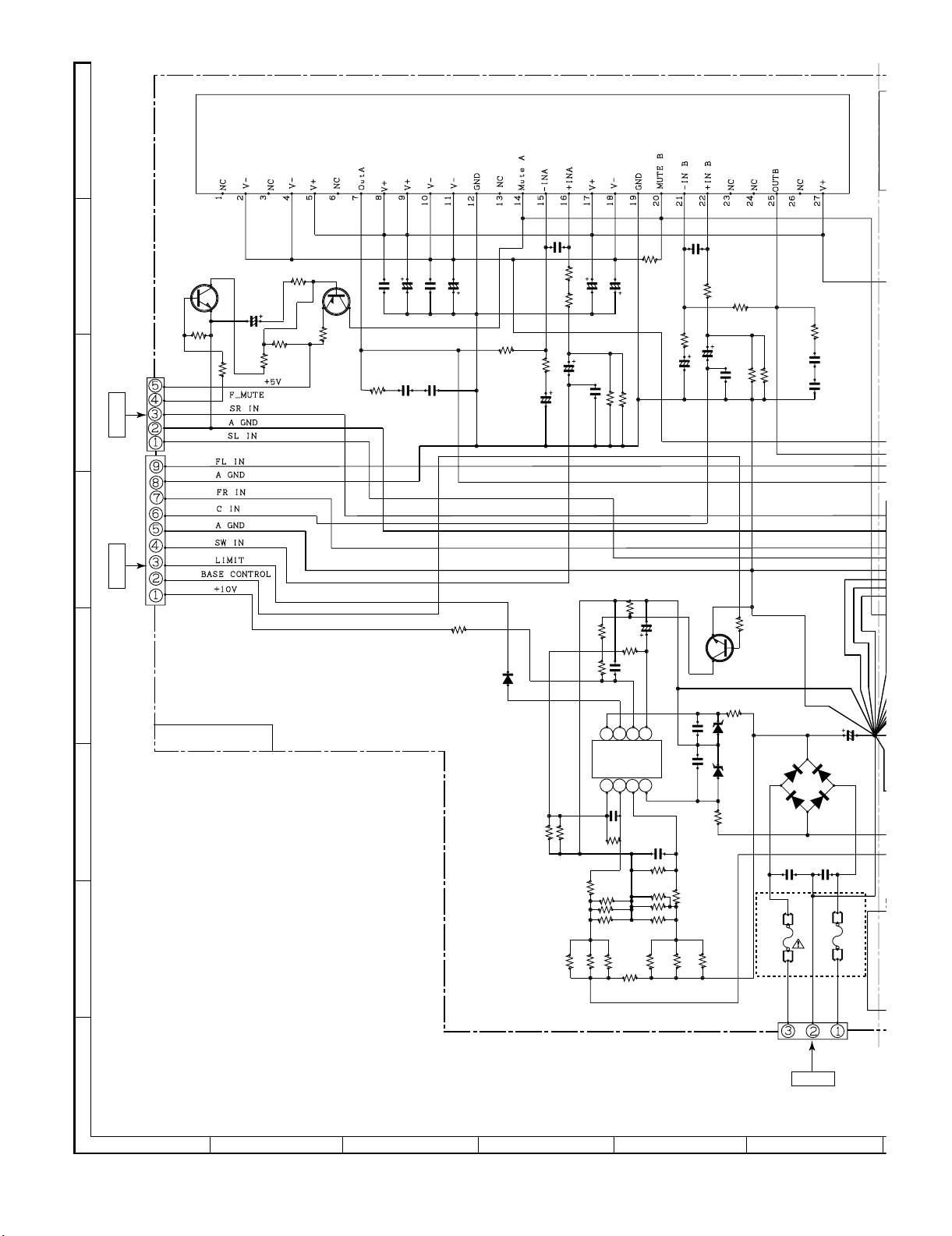
• NOTES ON SCHEMATIC DIAGRAM can be found on page 5-1.
1
23456
Figure 6-1 SCHEMATIC DIAGRAM (1/10)
6 – 1
VOL
C226
47/16
Page 27
HT-X1
12K
1
R864
1K
22K
1N4148
Q444
100K
1N4148
D420
KTC3199 GR
R838
1N4148
D419
100K
100K
R833
R832
1N4148
D416
ZD425
DZH03C3
R869
R862
3.3K
Q437
R863
KTC3200 GR
10K
R863A
10K
C478A
Q437A
R862A
KTC3200 GR
3.3K
1K
R869A
C464
0.0022
R831
100K
R840
100K
100K
1N4148
1N4148
D417
D418
1N4148
D421
D432
1N4148
7
9GR
433
4148
RLY401
1N4004
R470
R471
RLY402
D426
D425
1N4004
56K
56K
1N4004
1N4148
Q432
KRA107 M
RLY403
D424
D422
2HC1815 GR
Q429
2HC1815 GR
Q433
KRC107 M
1
3
3
2
2
1
C463
3.3/16
R917
0.2(1/2W)
12K
R918
0.022
C814
D429
R919
6.2K
R839
R473 56K
R474 56K
Q430
R848 56K
R829 56K
R856
5.6K
C465
47/50
R460
330K
C470
100/16
D427
1N4004
C478
47/16
D427A
47/16
1N4004
R864A
22K
D411
1N4148
Q436
2SC535 C
Q436A
2SC535 C
R865
470K
R865A
Q415
470K
R923
0.2(1/2W)
C815
0.022
R922
6.2K
2HC1815 GR
C479
C479A
Q438A
12K
R924
R475
5.6K
Q416
2HC1815 GR
R866
27K
Q438
KTA1266 GR
10/16
10/16
KTA1266 GR
D436
D437
D431
1N4148
Q445
KTC3199 GR
R867
R867A
33
R866A
C806
33
27K
47/50
R868
3.3K
R868A
3.3K
Q439A
2HC1815 GR
1N4148
1N4148
Q439
2HC1815 GR
1
2
3
4
CNP205
R475A
1
M
M401
2
3
M
4
M402
BI205
R834
10K
4.7
C426
0.1
C490
0.1
C822
0.0047
C496
0.0047
C440
C429
0.0047
0.1
C434
0.1
R835
4.7
C435
0.1
C803
0.1
R843
4.7
R841
4.7
C438
0.1
C452
0.1
C449
0.0047
0.1
C442
C443
0.1
R842
4.7
C444
0.1
C445
0.0047
0.1
C446
4.7
R850
C495
0.0047
C827
0.0047
C823
C824
0.0047
C433
0.0047
C825
0.0047
C826
0.0047
CNP206
0.0047
+
-
+
-
+
-
+
-
+
-
1
2
3
SPEAKER TERMINAL
+
-
+
-
+
-
+
-
+
-
SO401
CFW3
82
C217
0.047
KIA7805API
IC203
AN78L05
1
C225
0.047
321
IC201
IC201
2
3
D216
1N4004
D209
1N4004
C232
2200/16
R201
C216
47/25
VOLTAGE REGULATOR
VOLTAGE REGULATOR
C226
47/16
7
C218
220/25
D206
D205
0.1
C208
1N5402M
C224
R203
R204
3300/25
12K
330
C210
100/50
D207
C211
47/50
ZD202
DZH06C2
330
R205
R210
10K
C207
2.7K
R216
0.1
6800/25
C206
321
82
R202
C227
0.047
IC202
K
IA7812API
C219
0.022
VOLTAGE
R
EGULAT
OR
C228
0.047
D217
D218
1N4004
D220
D219
C229
0.047
T202
SUB POWER
TRANSFORMER
D208
47K
R208
R207
10
2HC1815 GR
47K
R218
C212
47/50
KTA1266 GR
Q203
R958
0.1
C209
C215
100/50
D210
ZD201
DZH3001
C206A
0.1
R206
Q201
D221
1N4004
4.7M
1N4004
D212
C214
1N4004
47/63
D211
C213
220/50
1N4004
1K
RLY400
BI203
CNS203
CNP203
F201
2A/120V
CNP204
LINE FILTER
LF201
POWER2 PWB-A3
P6-3 6-H
AMP PWB
CNP202
CNS202
AC SOCKET
TO
CNS204
SO202
T201
POWER TRANSFORMER
CNP201
CNS202
CNS201
AC POWER
SUPPLY CORD
AC 120 V,
60 Hz
8 9 10 11 12
Figure 6-2 SCHEMATIC DIAGRAM (2/10)
6 – 2
Page 28
HT-X1
IC101
150P
0
JB101
1K
R101
C107
C110
150P
1/50
C/SW
10/50
C105
10/50
C106
82K
R106A
82K
R106
R119
12K
R137
470
C108
R115
47/50
C202
150P
R123
1K
18K
4.7
82K
R108A
R191
C192
0.022
C193
0.022
C109
1/50
C126
150P
82K
R108
0.1
C103
C191
0.022
10/50
C104
POWER AMP.
LM4732TA
C201
R113
18K
R146
470
C111
47/50
A
Q102
CNP402A
KTC3199 GR
R198
10K
R196
4.7K
C151
2.2/16
R172
1K
B
FROM
P6-1 5-A
POWER1 PWB
C
CNS402A
R197
R173
470K
0
+B
Q101
KTA1266 GR
620
R175
R190
4.7
0.1
C101
10/50
C102
C190
0.022
D
CNS402B
CNP402B
10K
P6-1 5-A
FROM
POWER1 PWB
+B
E
AMP PWB-A1
R154
D102
1N4148
IC104
BUFFER
AMP.
F
R157
120K
R981
R159
10K
R979
18K
G
R165
18K
270
R153
3.3K
R152
NJM4558D
C137
0.0022
R169
120K
180K
R980
R167
18K
18K
R164
8
IC104
1
18K
R171
1.2K
R156
10K
C132
0.1
7
2
18K
R163
R166
0.1/3W
C133
1/50
C134
0.1
5
6
0.1
C153
4
3
C136
0.0022
R158
180K
R977
18K
R168
18K
R160
18K
R978
18K
R170
R162
10K
18K
KTC3199 GR
1K
R155
18K
R161
R181
1K
ZD101
ZD102
R199
Q103
DZH1602
DZH1602
CNP202
2.2K
+B
C130
F102
6.3A/125V
C128
4700/50
D101
GBJ10GM
C131
0.1
0.1
F101
6.3A/125V
H
• NOTES ON SCHEMATIC DIAGRAM can be found on page 5-1.
1
23456
Figure 6-3 SCHEMATIC DIAGRAM (3/10)
6 – 3
CNS202
P6-2 11-F
FROM
MAIN POWER TRANSFORMER
Page 29

HT-X1
IC102
POWER AMP.
FL/FR
LM4732TA
C204
150P
150P
47/50
R104
C203
R118
1K
18K
R193
82K
R116A
82K
R116
4.7
C196
0.022
C197
0.022
CNP401
CNS401
C124
1/50
150P
C125
10/50
82K
R107A
C118
10/50
82K
R107
R111
12K
R151
470
C123
0
C119
47/50
R149
470
JR401
R103
1K
C117
C120
1/50
C121
150P
0.1
C114
18K
10/50
C115
0.1
10/50
C116
C113
R112
C195
0.022
2
2
3
2
C194
R192
0.022
4.7
1
GM
F101
6.3A/125V
C129
4700/50
C127
0.1
82K
R109A
R121
82K
R109
150P
C166
C168
1/50
18K
C206B
150P
R105
FROM
P6-1 6-A
POWER1 PWB
C199
C198
0.022
SL/SR
C174
10/50
C189
0.022
R122
18K
82K
82K
C169
R117
C173
C112
1/50
10/50
R102
150P
1K
JB103
C172
47/50
470
R134
0
C205
150P
47/50
R110
12K
R117A
C170
10/50
C167
470
R147
1K
IC103
POWER AMP.
C175
0.022
0.1
C188
0.022
C176
10/50
R194
4.7
R195
C177
4.7
0.1
LM4732TA
ORMER
7
8 9 10 11 12
Figure 6-4 SCHEMATIC DIAGRAM (4/10)
6 – 4
Page 30

HT-X1
CA6
6
0
3
O
R564
A
B
C
DVD SERVO PEB UNIT
D
E
F
G
J1
P6-21 4-C
TO
P6-1 1-C
TO
POWER1 PWB
S101B
P6-1 1-F
TO
POWER1 PWB
S102B
CNS501
BI501
S101A
1
2
3
4
5
6
7
8
9
10
11
12
13
1
2
3
4
5
6
7
8
9
10
11
12
13
C672
0.047
S102A
IC503
LM2576T
27K
R526A
C527
47/16
R526
27K
C526
R525
C525
0.001
9.1K
10/16
C530
10/16
27K
R531A
27K
R514A
R502A
C506
+B
10/16
R507A
NC
JP5
0
JP4
0
C5B4
0.0022
+B
+B
NC
-B
+B
CNW508A
C531
R530
0.001
9.1K
R531
C533
27K
47P
C515
47/16
R514
27K
R513
C514
C513
9.1K
10/16
0.001
C518
C519
R518
10/16
27K
R519A
27K
C501
10/16
R506
9.1K
27K
-B
NJM14558
0.001
9.1K
R519
27K
R502
C503
47/16
27K
C502
R501
0.001
9.1K
C507
NJM14558
0.001
R507
27K
C5B2
0.0022
+B
+B
3.3K
R527
1
34
2
IC509
NJM14558
5678
3.3K
R532
R533
30K
3.3K
R515
34
21
IC508
5678
C521
47P
R520
3.3K
R521
30K
+B
3.3K
R503
34
21
IC506
567
8
150P
C509
3.3K
R508
R509
C528
47P
C516
47P
120K
C522
10/16
C504
47P
R528
C534
10/16
47/16
C510C
R516
C510B
R504
47/16
C510A
+B
30K
30K
C510
10/16
C529
10/16
C517
10/16
30K
10/16
C505
R535
R524
R523
47/16
R511
R529
10K
R536
10K
R534
10
C512C
R517
10K
10K
R522
10
R505
10K
R512
C512A
-B
10
10
10K
R510
+B
10
C524
C523
C511
10
0.1
22P
C536
0.1
22P 22P
C512B
22P
22P
C512
+B
C529A
10/16
C590
R590D
27K
R590E
27K
+B
IC507
CD4053M
12345678
0.047
C538
R541
10K
C545
47/16
C544
10/16
C550
0.015
CNP702
R538
47K
R542
47/16
R590A
0.22
C670
100K
R548
R590B
18K
27K
910111213141516
C594
22/25
R541A
C539
0.0033
R539
8.2K
8.2K
R543
0.1
C546
C548
220P
1.5K
P6-7 1-G
FROM
DISPLAY PWB
CNW702
R5C2
R5C1
27K
R539A
27K
IC504
BUFFER
NJM4558D
270
R540
C543
47/25
C549
10/16
R549
100K
R550
100K
22P
C535
C529B
10/16
27K
R630
R590C
100
+B
0.1
10/16
10/16
C500C
C529C
+B
0.0022
CNW301
P6-10 12-D
FROM
TUNER PWB
CNW508B
C5B1
CNP301
0.1
C586A
+B
C598
22/25
R618
100
47/25
C537
C541
10/16
C540
10/16
10K
R537
R544
10K
10K
R545
R547
100K
C547
R546
220
2.2/50
+B
+B
-B
+B
VOLTAGE REGULATOR
+B
0.1
C5B3
C599
100/25
IC501
KIA7812API
VOLTAGE
REGULATOR
180
+B
180
R543A
C543A
27K
47/16
1N4004
C596
22/25
IC502
KIA7805API
VOLTAGE REGULATOR
100
R629
C552
220P
L502
2.2uH
C553
220P
C554
220P
R542A 27K
C582C
10/16
47/16
C582A
R575
27K
C582B
10/16
D507
R576
L501 100uH
1N5822
R590
100/25
1
1
D505
C555
100/16
CL
DI
R572
10K
D508
3
2
C588
+B
D506
1N4004
3
2
C592
0.047
1N4004
10K
100K
C556
33/16
C558
22/16
C557
VREF
VDD
ROUT
LOUT
VSS
CE
C565
2.2/16
C566
R552
IC512
NJM14558
567
R578
10
0.047
R555
3.9K
0.1
LBS
0.1
3.9K
34
R593
120
Q502
2SD601 AR
C560
0.1
C559
RBS
LTRE
0.1
0.0027
C567
C568
21
2
1
C589
47/25
+B
C580
47/16
R556
47K
R557
0.0027
10K
C561
2.2/50
RTRE
RSL0
RIN
LSL0
LIN
C569
2.2/50
R554
10K
47K
R553
27K
R579
IC512
8
PER AMP.
10K
R577
C585
R595
470/16
1K
3
1
1K
R595A
2
100K
Q501
KRA107 M
R592
R591
IC511
KIA7805API
VOLTAGE
REGULATOR
+B
R566 1K
R567 1K
R568 1K
C562
R559
4.7/50
1K
R4R3R2
L4
C570
4.7/50
10/16
C582D
10/16
C582E
47P
C532B
47P
C532A
D509
1N4148
3
1K
C564
R1
L1L2L3
R561
LC75
AUDI
1K
R699
10K
IC5
C571
10/16
10/1
R569
C584
+B
R589
R551
100K
27K
R574
27K
R573
27K
H
• NOTES ON SCHEMATIC DIAGRAM can be found on page 5-1.
1
23456
Figure 6-5 SCHEMATIC DIAGRAM (5/10)
6 – 5
Page 31

D509
O
1
1N4148
R699
10K
3
Q501
A107 M
R592
1K
IC511
7805API
66 1K
67 1K
68 1K
C564
10/16
59
K
IC505
R1
LC75341M
L1
AUDIO
PROCESSOR
R561
1K
C571
10/16
+B
123
R594
22K
R564
R562
3.9K
22K
R569
56
R565
3.9K
L5A1
CFW5
J2
C586
+B
0.1
TUN R
AUX L
TUN L
AUX R
P6-21 1-B
FROM
DVD SERVO PWB
CNS502
BI502
C587
220/10
HT-X1
P6-7 1-F
CNW704
FROM
DISPLAY PWB
CNP704
+B
+B
10uH
CL
CE
DI
0
JP6
+B
+B
+B
+B
L513B
C576
330P
R597
L513A
C577
R571
C5A1
0.0022
R586
10K
Q503
2HC1815 GR
47K
330P
47K
C599B
C599A
Q518
KTC3199 GR
R601
0.00220.0022
3.3K
R602
3.3K
Q517
KTC3199 GR
470/16
R587
1.2K
R588
1.2K
CFW1
R604
10K
C667
CFW2
R606
100K
C641
C665
220/16
R627
100
+B
Q504
2SB562 C
R605
100K
R608
R609
R610
R611
82K
C640
82
100/16
R607
12 3 4
82
C639
100/16
82
C637
82
0.022
R612
2.7K
C638
33P
IC510
5678
R614
33P
2.7K
R613
82K
IC510
NJM4558D
BUFFER
R510C
10/16
C500A
10/16
C500B
10/16
R510B
3.3K
C634
R615
27K
R616
C667A
27K
C633
10/16
47/16
2.2K
R5B3
27K
R615A
27K
1K
R616A
R617
R510D
2.2K
Q524
KTC3199 GR
470
R5B4
1K
KTC3199 GR
R619
470
Q5A3
R5B1
3.3K
R5B2
3.3K
R510A
Q5A4
KTC3199 GR
3.3K
KTC3199 GR
R707
Q525
0
MAIN PWB-B2
C5A5
0.0022
BI503
BI506
CNS506
J6
P6-22 5-D
TO
DVD SERV
PWB
CNS503
10
10
9
9
8
8
7
7
6
6
5
5
4
4
3
3
2
1
J3
6-22 8-C
TO
DVD SERVO
PWB
2
1
C5A6
0.0022
C5A9
0.0022
L503
C572
10/16
1K
0.1
C581
2 1
3
S503
DIGITAL IN
7
R700
C573
0.1
S501
AUX IN
8 9 10 11 12
R596
L513
+B
680
10uH
1K
L504
0
0
JP3
JP2
D512
C5A4
0.0022
1N4148W
CFW4
2K
R684
D511
R687
C591
47/16
1N4004
Q521
2SB561 C
2SD601 AR
Q522
R688
R689
10K
1.5K
CFW6
0
75
R584
R585
L507
L506
S504
C5A8
0.0022
L508
C5A7
0.0022
L514
1N4148W
D504
D503
C574
1N4148W
0.001
0.0022
C575
0
75
R581
R582
L510
L509
COMPONENT
VIDEO OUT
L511
S505
Figure 6-6 SCHEMATIC DIAGRAM (6/10)
6 – 6
Page 32

HT-X1
A
-B
+B
DISPLAY PWB-B1
B
+B +B
-B
R730 10K
+B
10K
R772
R789 10K
R790 10K
+B
+B
10K
R768
+B
+B
+B
+B
R702 10K
R706 10K
R719
10K
D706
1N4004
R792
10K
C701
+B
0.1
10K
R735
+B
D701 1N4004
C
BI302
CNS302
CNP302
D
P6-10 12-C
TO
TUNER PWB
CNW703
J5
P6-19 1-D
TO
DVD SERVO
PWB
E
F
G
CNP704
P6-6 8-A
TO
MAIN PWB
CNP702
P6-5 5-G
TO
MAIN PWB
CNW704
CNW702
LDE PWB-B3
D707
1N4148
LPBB73V1
LED702
CNW707
+B
+B
-B
-B
D708
1N4004
+B
CNP707
+B
220
R787
-B -B
+B
-B
+B
+B
KTA1266 GR
+B
-B
R774
47K
Q702
KRC107 M
R783
2.2K
3
2
Q701
1
H
C702
0.1
R791 1K
R767 1K
R769 1K
R750 1K
R755 1K
R716 1K
R731 1K
R701 1K
R724 1K
R725 1K
R76 1K
R747 1K
R748 1K
R749 1K
R728 1K
R729 1K
L704
R735A
-B
1K
1K
1K
R705
R713
R721
1K
1K
R727
R722
1K
R723
1K
R720
1K
R712
SYSTEM MICROCOMPUTER
1K
1K
1K
R737
R703
R7391KR7381KR736
22P(CH)
C703
C704
0.82uH
10K
10K
10K
R797
R735B
22P(CH)
32.768MHz
10K
R745
SW700
JOG VOLUME
IC701
IX0058SJ
1K
R740
R741
10M
X701
C707
C706
220/10
+B
C714
0.001
D706A
1N4148
D706B
1N4148
+B
R753A 82K
R753B 82K
R753C 82K
R753D 82K
R753E 82K
R753F 82K
R753G 82K
R753H 82K
R753I 82K
R753J 82K
R753K 82K
R753L 82K
R753M 82K
R753N 82K
R753P 82K
R753Q 82K
R753R 82K
R753S 82K
R753T 82K
R753U 82K
X702
8 MHz
R746
0
+B
0.1
C706A
R742
R708 1K
0.0047
R709 1K
10K
R743
CFW9
+B
-B
-B
+B
R770 1K
R715 1K
R714 1K
R710 1K
10K
R744
10K
C715
0.001
R732 1K
10K
R788
R734
10K
• NOTES ON SCHEMATIC DIAGRAM can be found on page 5-1.
1
23456
Figure 6-7 SCHEMATIC DIAGRAM (7/10)
6 – 7
Page 33

VFD701
R714 1K
FL DISPLAY
HT-X1
-B
JK1
C015
CFW6A
GP1UD261
1K
R751
C709
100/10
0.1
RX701
C014
C016
321
C710
HEADPHONES
0.1
0.022
0.047
270P
C599C
270P
CNW705
-B
R752A 82K
R752B 82K
R752C 82K
R752D 82K
R752E 82K
R752F 82K
R752G 82K
R752H 82K
R752I 82K
R752J 82K
R752K 82K
R752L 82K
R752M 82K
R752N 82K
R752P 82K
R752Q 82K
R752R 82K
R752S 82K
R752T 82K
R752U 82K
R754
10K
-B
+B
+B
C599D
CNP705
R794A
L706
R795A
C708
HEADPHONES PWB-B6
68
2.2uH
68
100P
C705
0.1
+B
SWITCH PWB-B4
SW708
SW706
SW705
RX702
GP1UD261
C719
100P
R782
1.5K
R781
1.2K
R780
1.2K
321
CNP706
P6-23 1-B
FROM
DVD SERV PWB
J4
Q505
47/16
C720
Q510
KTC3203 Y
KTA1271 Y
KTC3199 GR
R758
470
R757
390
Q506
22K
R784
Q507
KTC3199 GR
R785
22K
+B
Q508
KTA1271 Y
Q509
R759
KTC3203 Y
470
390
R786
SW704 SW707
R766
SW703
+B
R715 1K
R718 1K
R732 1K
10K
R734
10K
+B
0.82uH
R704
L703
+B
L701
+B
0.82uH
0.82uH
L705
+B
CNW609
CNP609
+B
+B
D703
1N4148
D702
1N4148
R760B 47
R760A 47
+B
R763
D704
3.3K
Q709
1N4148
KRC107 M
R762
1K
R761
+B
1K
C711
+B
3
2
1
+B
D705
0.1
1N4148
+B
R776 1K
Q703
KTC3199 GR
R775
82
R777
10K
R778
10K
KTC3199 GR
C712
33/16
C713
0.01
R764
100K
1.2K
R765
SW702
1.2K
SW701
0.047
100/10
C717
C718
R756
1K
+B
ZD701
DZH03C3
R779
120
Q704
C716
R793
47/16
1K
7
8 9 10 11 12
Figure 6-8 SCHEMATIC DIAGRAM (8/10)
6 – 8
Page 34

HT-X1
PHASE
MO/ST
3
/
R376
0.022
A
B
TUNER PWB-B5
R380
1.5K
1K
R373
VSM
C392
C364 10/16
R352
0.001
1K
R372
AM IF
CF352
AIN
0.022
C365
AM LOW
IN
1K
1K
R371
CUT
GND
C380
DO
IC303
0.001
C366
FM/AM
C353 0.022
10/16
PD
OUT
SD
R379
L354
2.2K
C387
C354
R350
C367
VDD
0
1/50
STEREO
0.022
0.022
R353
CF351
FM IN
C374
0.018
R357
470K
0
R356
X351
456 KHz
C368
1/50
MPX VCO
VCC
FM DET
270
100/10
0.022
C398
C399
+B
R395
R393
1K
R377
5.6K
L351
100uH
0.01
C385
NC
NC
AM IN
I
FMFMMUTE
MO/ST
IF REQ
R359
1.8K
R360
4.7K
C373
0.018
C371
1/50
56P
C369
C
1
OUT
OUT
R-CH
L-CH
MPX IN
PHASE
IF OUT
C358
1/50
C357
0.001
2.2/50
C356
C370
1/50
C355
22P
C383
47K
5.6K
R387
C386
330P
FIN
R365
10K
T302
33P
3.3/50
C343
8.2K
C362
C360 0.022
OUT
AM OSC
AM OSC
IN
OUT
AM MIX
FM IF
+B
C352
10/16
C378
330P
C344
33P
C397
R382
330
R386
330
C381
12P(CH)
X352
4.5 MHz
C382
15P(CH)
C384
0.001
C329
0.022
T306
C346
68
R369A
0.022
C388
0.047
C330
C335
560P
R369B
82
L342
2.2uH
0.022
C345
IC301
4.7K
R345
12P(CH)
R323
C348
C331
68K
100/16
R343
0.047
0.022
C332
VD301
SVC348S
+B
5.6K
R347
IC301
6.8K
R313
R336
Q301
2SC380 O
33
R349
680
C334
27P(UJ)
NSA003SJ
FM FRONT END
C341
0.022
+B
R346
330
CF303
R344
680
180
C347
0.022
C302
C301
C349
D301
D302
0.001
L301
D303
D304
1N4148
1N4148
1N4148
0.012
0.001
1N4148
C376
0.022
C337
0.01
C
SO302
TERMINAL
AM ANTENNA
D
TERMINAL
FM ANTENNA
SO301
E
VR351
R351
C351 0.022
5.6K
L353
1mH
CF302
R358
+B
FM SIGNAL
AM SIGNAL
+B
F
+B
FM IF DET. /FM MPX./AM IF
0.022
C363
C361 0.022
IN
IN
AM RF
FM AFC
IC303
LA1832S
REG
C350
0.022
T351
AM IF
0.022
C394
47/16
VT
C393
10K
R381
1/50
VSS
IC302
AOUT
XOUTXIN
LC72131
CEDICL
NC
IC302
1K
TUNER
(PLL)
R374
G
H
• NOTES ON SCHEMATIC DIAGRAM can be found on page 5-1.
1
23456
Figure 6-9 SCHEMATIC DIAGRAM (9/10)
6 – 9
Page 35

IF OUT
C369
C355
330P
HT-X1
C374
0.018
56P
OUT
R-CH
PHASE
C357
2.2/50
22P
R387
R365
L-CH
C358
C370
Q351
KRC104 M
R361
R376
0
(AM/FM)
R355
10K
2
R362
0
3.3K
L352
100uH
C396
100/10
R391
390
R392
390
KTA1266 GR
1
3
CNP302
7
P6-7 1-D
+B+B
CNP301
6
FROM
DISPLAY PWB
5
4
CNS302
3
2
1
P6-5 4-F
FROM
MAIN PWB
CNW301
R366
2.2K
+B
ZD351
DZH05C2
C395
0.022
Q360
10.8V
11.7V
R383
5.6K
10.9V
+B
R385
5.6K
R384
6.8K
C391
47/16
C373
0.018
C371
1/50
C372
1/50
OUT
MO/ST
PHASE
1/50
1/50
C383
0.022
5.6K
10K
D308
1N4148
+B
C324
C325
0.022
100/16
R399
10
7
8 9 10 11 12
Figure 6-10 SCHEMATIC DIAGRAM (10/10)
6 – 10
Page 36
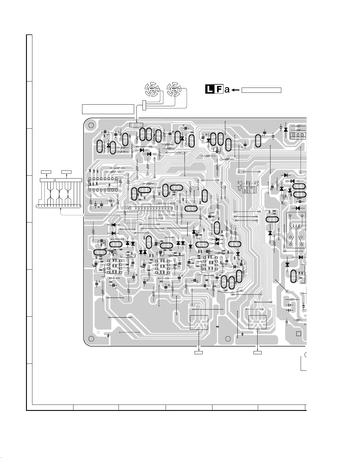
HT-X1
D421
8
4
R840
R927
R
-
[2] Wiring side of PWB
A
B
POWER1 PWB-A2
M401
FAN MOTOR
M401
FAN MOTOR
Lead-free solder indication
BK
1
RD
2
WH
3
BK
4
BI205
Lead-free solder is used in this Power1 PWB.
Refer to "Precautions for handling lead-free solder" for instructions
and precautions.
C478
R863
E
C
Q437
C
P6-17 4-B
AMP. PWB
CNS402A
CNS402A
RD
RD
D
1
P6-17 4-F
TO
GY
GY
TO
AMP. PWB
CNS402B
CNS402B
12
34
5
678954321
BK
RD
RD
BK
BK
WH
BR
RD
RD
GYGYGY
WH
WH
BR
RDGYWH
BK
RD
WHBKRDBRWHBKRD
15
BI402
E
F
B
R972
R973
R974
1
2 3 4 5 6 7 8
C453
C451
C450
IC407
16 15 14 13 12 11 10 9
R909
C481
C484
R897
C811
R898
R449
Q407
BCE
R961
R960
C235
R428
C414
R426
R444
R443
C422
R440
CNP205
R867
Q438
C479
Q436
E
R864
C
R865
B
D427
R862
R491
R492
R976
C903
C485
R489
R487
R895
D441
D440
Q408
ECB
R962
R963
R448
R436A
C422A
R441A
4
5
R434
R441
R436
3
6
R433
C420
2
7
1
8
C421
R442
IC405
C415
C416
C904
4231
Q439A
Q438A
E
E
Q439
B
R866
R868
C
E
D436
R869
R490
R493
E
C
Q454
R949
B
R902
1
D443
D442
C236
R445
R447
D452
C425
R414
R435
C488
R437
B
C
C
R866A
C
B
B
D437
R475A
R983
Q456
BCE
R951
R950
BI402
B
R423
C
Q403
E
R965
D453
C233
C405
R415
R405
C401
C479A
E
R867A
R864A
R868A
R865A
R869A
Q457
E
C
B
R955
R952
R424
C810
Q404
R896
R967
C402A
R409A
R964
R407A
4
5
R407
R409
3
6
R410
C404
2
7
R406
1
8
C403
R408
IC404
C411
C412
R401
C478A
Q436A
R863A
E
E
C
C
B
B
R862A
D427A
Q437A
Q458
R984
BCE
R954
R953
R956
R958
15
R957
D455
ECB
C234
R966
R425
R870
R412
C413
R411
C402
R402
D454
R463
Q455
R450
C489
Q459
R959
ECB
R899
D457
R900
C812
Q409
D456
CE
R968
C237
R452
R457
R458
C497
S101B
12 3 4
87 6 5
9101112
13
Q434
Q435
E
B
C256
ZD423
C216A
R494
E
C
B
C813
R451
B
C497A
R969
4
R459
3
R462
2
1
R456
IC406
C494
C417
Q433
C
C
1
B
E
2
C463
3
R859
R860
R861
R901
R908
R808
B
Q412
C
R971
R836
E
R942
R943
R970
D459
Q453
R459A
R467
R461A
R461
D458
5
6
R466
C498
7
8
C431
C801
R938
C821
ECB
C238
R468
ZD424
R477
R975
C802
C902
R946
C901
R465
E
Q450
Q452
Q451
C
E
R982
3
B
C
2
B
1
R944
R941
C820
R945
8765
1
2
Q432
3
S102B
1234
9101112
13
C216
C464
C470
C814
R918
Q444
D429
R917
R202
C217
R201
1 2 3
D209
IC201
ZD425
D410
R460
R919
ECB
Q413
ECB
Q414
D420
R471
R470
RLY402
C434
BCE
R472
R839
C809
D426
D433
R923
Q445
C815
E
R922
C
R924
B
R
R835
C426
C
C822
D419
R838
D431
C429
C496
G
S101A
P6-16 10-A
FROM
MAIN PWB
S101A
P6-16 9-A
FROM
MAIN PWB
H
1
23456
Figure 6-11 WIRING SIDE OF PWB (1/7)
6 – 11
Page 37
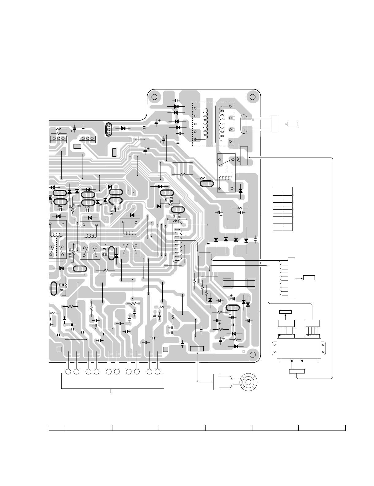
HT-X1
R202
R201
IC201
C218
C219
IC202
IC203
D216
C227
C232
C226
C225
D218
C228
D217
D219
D220
C229
C206
CNP201
BI203
CNS203
CNP203
P6-17 6-F
TO
POWER2 PWB
RD
RD
BK
BK
R216
RLY400
C224
D221
Q203
R218
R210
Q448
R934
R914
Q443
D435
D434
C207
D425
Q430
Q429
C465
D422
D416
D417
D424
D411
Q416
Q415
C806
D418
R831
D421
C809
Q414
Q413
D426
D410
Q445
R923
D433
R925
Q446
RLY403
LY402
R928
Q447
D432
RLY401
BI401
R204
R985
R205
R203
C208
ZD202
CNP204
F201
2A/125V
D205
C210
D206
D207
C215
D212
D208
D210
C209
C214
D211
ZD201
R206
C206A
C212
Q201
R208
R207
C213
C211
CNP206
C827
C495
C446
C444
R850
R841
C438
C826
C452
C445
R842
C442
C443
C825
C449
C824
C433
C803
C435
R843
C823
R834
C440
C426
C490
C822
FRONT SPEAKER
L-CH R-CH
SO401
SPEAKER TERMINAL
SURROUD SPEAKER
L-CH
R-CH
CENTER
SPEAKER
R835
C818
R933
R936
C819
R932
R915
R856
R848
R833
R829
R832
R475
R473
R474
R840
R472
R839
R922
C815
R924
R927
R926
C816
R930
C817
R931
BR
COLOR TABLE
RD(R)
OR
YL
GR
BL
VL
GY
WH(W)
BK
PK
BROWN
RED
ORANGE
YELLOW
GREEN
BLUE
VIOLET
GRAY
WHITE
BLACK
PINK
ECB
ECB
BCE
BCE
ECB
B
C
E
E
C
B
EC B
ECB
ECB
ECB
BCE
BCE
2
2
3
1
11
1
1
1
SUBWOOFER
2
1
CNS401
CNP401
P6-17 5-E
TO
AMP. PWB
GY
GY
GY
GY
GY
GY
GY
GY
GY
BK
10
9
8
7
6
5
4
3
2
1
432 1
CNP202
BLBKBL
BKBKYL
CNS202
P6-17 3-A
TO
AMP. PWB
T201
MAIN POWER
TRANSFORMER
T202
SUB POWER
TRANSFORMER
BK
BR
123
YL
1234
CNS204
1
1
32
3
CNS201
1 2 3 1
1
3
2
2 3
+
-
+
-
+
-
+
-
+
-
7
8 9 10 11 12
Figure 6-12 WIRING SIDE OF PWB (2/7)
6 – 12
Page 38
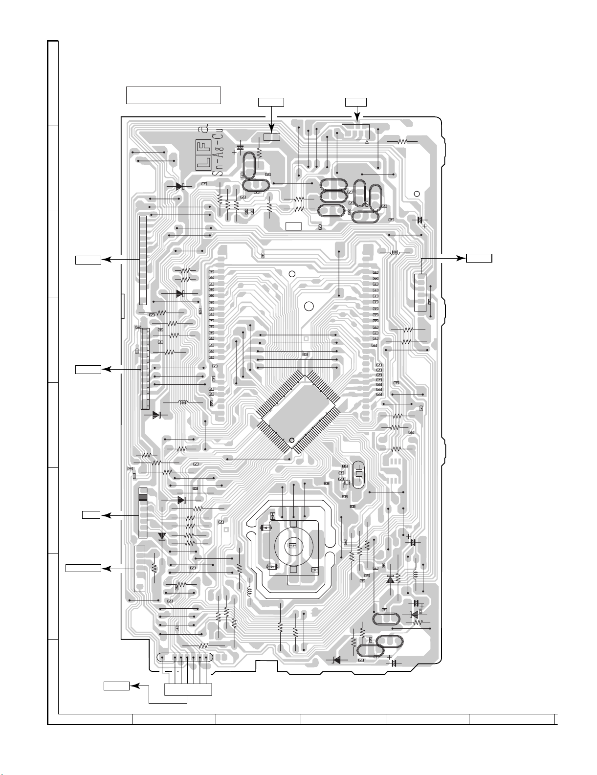
HT-X1
A
A
DISPLAY PWB-B1
DISPLAY PWB-B1
P6-15 5-G
P6-15 5-G
FROM
FROM
LED PWB
LED PWB
CNW707
CNW707
P6-18 2-B
P6-18 2-B
FROM
FROM
DVD SERVO
DVD SERVO
PWB
PWB
J4
J4
B
B
C
C
D
D
E
E
F
F
G
G
H
H
P6-15 2-E
P6-15 2-E
TO
TO
MAIN PWB
MAIN PWB
CNP704
CNP704
P6-15 1-A
P6-15 1-A
TO
TO
MAIN PWB
MAIN PWB
CNP702
CNP702
P6-18 2-4
P6-18 2-4
TO
DVD SERVO
DVD SERVO
PWB
PWB
J5
P6-15 6-F
P6-15 6-F
TO
TO
SWITCH PWB
SWITCH PWB
CNP609
CNP609
1
TO
J5
1
CNP302
CNP302
P6-14 9-H
P6-14 9-H
TO
TO
TUNER PWB
TUNER PWB
14
14
13
13
12
12
11
11
10
10
9
9
8
8
7
7
6
6
5
5
4
4
3
3
1
1
R768
R768
CNW702
CNW702
R730
R730
CNW703
CNW703
R759
X702
R710
R710
R759
E
E
C
C
B
B
R715
R714
R732
X702
R744
R744
R762
123
123
Q703
Q703
R778
R778
BCE
BCE
R777
R777
Q507
R785
R702
R715
R714
R732
R788
R762
Q704
Q507
R785
R702
L701
R704
R718
R790
R788
D704
Q704
C716
R760A
R760A
L701
R704
R718
R790
R763
D704
D705
BCE
C716
R763
D705
BCE
C709
C709
CNW705
CNW705
R776
R734
R734
C706
C706
L705
L705
C712
C712
R776
R764
C713
R764
R754
C713
HEADPHONES PWB
HEADPHONES PWB
R754
P6-15 3-G
P6-15 3-G
TO
TO
CNP705
CNP705
12
C720
E
C
B
R783
R783
321
R769
R769
R724
R735A
R739
R739
L704
R745
CNP707
Q701
Q701
E
C
R774
R774
B
321
R772
R772
R712
R735B
R735B
R735A
R789
R789
80
80
85
81
81
D706A
L704
R712
75
75
85
90
C706A
C706A
D706A
D706B
D706B
R761
70
70
90
95
100
100
SW700
R761
R706
R706
R713
R713
C705
65
65
IC701
95
C715
SW700
C705
55
60
60
IC701
5
5
1
C715
R738
R738
Q505
Q505
51
51
55
45
45
15
15
10
10
1
C711
C714
C714
C720
R76
D708
R76
D708
R720
R720
CNW704
CNW704
R721
R721
D703
D703
R767
R767
R792
R792
R719
R719
D702
D702
R731
R731
D701
R760B
R760B
CNW609
CNW609
1
1
R727
R770
D706
D701
R750
R705
R791
R750
R755
BK
1
C702
R705
R753I
R753J
R753J
R791
R753L
R753L
R753M
R753M
R727
R753N
R753N
R753P
R753P
R753S
R753S
R753T
R753T
L703
L703
R723
R723
R716
R770
R716
C701
C701
D706
R729
R729
R728
R728
R749
R749
R747
R747
R748
R748
J705
J705
R722
R722
R755
R701
R701
R735
R735
BI302
BI302
GYGYGYGYGY
BK
GYGYGYGYGY
234567
234567
1
23456
23456
C702
R753I
R753Q
R753R
R753U
GY
GY
R797
R753A
R753A
R753B
R753B
R753C
R753C
R753D
R753D
R753E
R753E
R753F
R753F
R753G
R753G
R753H
R753H
R753K
R753K
R753Q
R753R
R753U
R737
R737
R703
R703
7
7
CNS302
CNS302
R797
R725
R736
Q702
Q702
R725
R736
R724
R745
12
R787
CNP707
R787
R757
50
40
20
C711
50
40
35
20
R757
25
Q510
Q510
BCE
BCE
ECB
ECB
ECB
ECB
Q508
Q508
35
25
C703
R740
R740
R741
R741
C704
C704
ZD701
ZD701
CNP706
CNP706
R784
31
31
30
30
C703
C707
R746
R758
R758
R784
BCE
R786
R786
R752U
R752T
R752S
R752R
R752Q
R752P
R752N
R752M
R752L
R752K
R752J
R752I
R752H
X701
X701
C707
R746
R708
R708
R742
R793
R793
R779
Q506
Q506
E
E
C
C
B
B
BCE
Q509
Q509
R752U
R752T
R752S
R752R
R752Q
R752P
R752N
R752M
R752L
R752K
R752J
R752I
R752H
R752G
R752G
R752F
R752F
R752E
R752E
R752D
R752D
R752C
R752C
R752B
R752B
R752A
R752A
R709
R709
R743
R743
R742
Q709
Q709
R775
R775
R779
Figure 6-13 WIRING SIDE OF PWB (3/7)
6 – 13
Page 39

TUNER PWB-B5
Lead-free solder indication
Lead-free solder is used in this Display/Tuner PWB.
Refer to "Precautions for handling lead-free solder" for instructions
and precautions.
HT-X1
C329
L354
C374
D301
D302
T302
C331
C334
T306
R357
C373
C330
C337
R350
R356
C335R323
R362
R361
VD301
C362
C364
C366
C372
C371
C332
C367
C368
C369
R349
Q301
C343
R358
C344
C350
C365
R344
X351
C363
C346
CF303
123
ECB
24
23
22
R351
21
20
19
C360
18
17
16
15
14
13
3
2
1
C347
R336
R347
R313
1
2
3
4
C361
5
6
7
8
9
10
IC303
11
12
C354
C353
R393
R369A
1
2
3
R352
C399
C356
R369B
C348
CF302
CF352
R353
R376
VR351
C352
23
C351
CF351
C355
C358
1
C398
IC301
L353
T351
R355
R346
C385
C357
L342
C386
C378
C370
R345
C341
L352
R395
R377
R366
C345
C393
R343
IC302
C383
L351
R387
ZD351
2345678
C394
R380
Q360
BCE
R360
R384
C396
1
C387
R359
C380
R382
R383
R385
C395
C324
C397
R381
R365
R371
C392
C382
R372
R386
R392
R379
34567891011
R373
D321
R391
C391
C325
C381
2
R374
D308
2221201918171615141312
1
X352
C384
L301
D304
D303
C388
C301
1
2
C349
C376
AM LOOP ANTENA
C302
FM ANTENNA
SO302
TERMINAL
SO301
TERMINAL
Q351
CNP301
CNW301
P6-15 3-E
FROM
MAIN PWB
7
8 9 10 11 12
7
CNP302
CNS302
P6-13 2-H
FROM
DISPLAY PWB
R399
1
Figure 6-14 WIRING SIDE OF PWB (4/7)
6 – 14
Page 40

HT-X1
C505
C
A
B
C
D
MAIN PWB-B2
P6-13 1-D
FROM
DISPLAY PWB
CNW702
CNP702
C552
R552
R551
R553
C554
R554
C566
C567
R566
R589
L502
R550
R549
D511
C5A4
C555
CNW508B
24
20
1
C553
C565
C570
C599A
IC505
5
C569
C599B
D512
L513A
15
10
R561
C571
13
12
R557
R556
C562
R568
R700
C558
C559
C560
C568
R559
C564
CNP704
R565
R567
AUX IN
C577
C561
C582E
C532B
R569
S501
C557
R562
R571
R555
IC512
8
1
C582C
R564
R578
R596
C556
R579
5
R577
4
C582D
JP2
JP3
C576
R597
R629
C532A
R572
C582B
C548
CNW301
CNS506
L513
L513B
R573 R575
R574
R537
R544
C544
C549
R543
P6-18 6-D
J6
DVD SERVO PWB
L504
C5A5
C5A1
GY
GYGYGY
GY
BI506
C543A
R576
C5582A
C537
C536
R541A
R542A
C540
1
8
7
2
C539
R538
6
3
R543A
54
R539A
R548
R540
C543
TO
BK
C541
R541
IC504
C596
R542
C670
C546
R545
C545
R539
S505
COMPONENT VIDEO OUT
R582
R524
C514
R515
R514
R516
5
IC508
R517
C516
4
1
8
R514A
C547
R547
C550
R513
C513
R546
R581
C517
C524
R519A
R519
R522
C523
C510B
C521
C512B
R521
R520
R523
R518
C515
C519
C522
C518
BI501
R528
R527
C525
R525
R687
Q522
C591
R684
C529A
C526
C529
C528
4
58
IC509
R531
1
R529
R536
R526
R531A
L514
BCE
R689
C535
R535
C538
C512C
C510C
C533
R532
R530
C527
R526A
L509
R533
Q521
R688
C598
R534
C530
C534
C531
L511
C501
R504
R503
R507
R630
L510
C529B
R502
C503
R501
C504
I
CNW704
P6-13 1-C
FROM
DISPLAY PWB
E
SWITCH PWB-B4
F
G
HEADPHONES PWB-B6
R795A
JK1
HEADPHONES
C014
C016
C015
RX702
R794A
C799D
P6-14 9-H
TUNER PWB
DISPLAY PWB
L706
CNP301
TO
C717
P6-13 6-C
FROM
CNW705
C799C
C710
CNP705
RX701
C708
R751
J1
P6-18 6-G
TO
DVD SERVO PWB
R756
P6-13 3-A
TO
DISPLAY PWB
CNP707
P6-13 1-G
DISPLAY PWB
CNW609
C719
C718
LED PWB-B3
LED702
D707
FROM
CNP609
CNW707
H
1
23456
Figure 6-15 WIRING SIDE OF PWB (5/7)
6 – 15
Page 41

HT-X1
C501
R504
R503
R507
R630
L510
C529B
R502
C503
DVD SERVO PWB
CNS503
C505
R505
R501
C502
C512A
C504
1
4
5
8
IC506
P6-18 4-B
TO
J3
R585
L508
R584
C512
C511
R512
R511
R509
R502A
C510A
R507A
C594
R508
C509
R510
C510
C507
R506
C506
C5A7
C529C
R618
L507
R627
L506
C5A6
S504
S-VIDEO OUT
E
C
Q518
B
R604
C667
R5B2
R5B1
R601
R602
R510A
R609
R610
C665
R605
R608
E
C
B
Q5A4
BCE
BCE
BCE
Q525
8
C639
7
6
5
Q517
Q5A3
C5A8
R613
R616
C5A9
C641
R611
C638
R614
R615A
R510B
C637
R5B4
R606
R607
1
2
R612
3
IC510
4
R615
C633
R5B3
BCE
Q524
C500B
R616A
R617
P6-11 5-G
POWER1 PWB
S102A
56778
CNW508A
R510D
C640
C667A
R619
C500C
C634
C590
TO
S102B
13
RD
R510C
9101112
11234
C500A
R590D
16
15
1
R707
JP6
C672
C5B4
L5A
1
BI502
WHGYWHGYWH
R590E
9
10
5
C586A
8
IC507
R590C
1 2 3
IC511
R590
R699
R590A
R590B
C586
P6-11 4-G
POWER1 PWB
S101B
S101A
5678
GY
Q501
3
2
D509
1
R5C1
R5C2
C592
C587
R594
TO
13
C585
R595A
R592
IC502
3 2 1
C580
9101112
1234
R595
C581
C599
R591
Q502
D505
JP4
JP5
R593
D507
D508
L501
C5B1
D506
C5B2
C572
IC501
3
C573
C584
Q504
C5B3
2 1
C588
C574
C589
L503
R588
ECB
C575
S503
DIGITAL IN
Q503
ECB
D504
D503
IC503
1
2
3
4
5
R587
R586
P609
SW701
SW705
CNS502
J2
P6-18 4-H
TO
DVD SERVO PWB
SW706
R780
SW707
R781 R782
SW702
SW708
Lead-free solder indication
Lead-free solder is used in this Main/Switch PWB.
Refer to "Precautions for handling lead-free solder" for instructions
and precautions.
R765
SW703
SW704
R766
7
8 9 10 11 12
Figure 6-16 WIRING SIDE OF PWB (6/7)
6 – 16
Page 42

HT-X1
A
B
C
AMP PWB-A1
F102
6.3A/125V
F101
6.3A/125V
D101
C131
C128
C130
CNS202
CNP202
C129
P6-12 11-F
FROM
POWER TRANSFORMOR
C151
Q101
ECB
C127
ECB
Q102
3
2
1
CNP402A
C167
C172
R198
1272345
R117
R117A
R102
R109
C168
C166
R134
C174
C170
C175
C176
R147
C173
R175
C112
C169
R109A
R122
R197
R196
R105
C177
R172
R173
IC103
25
R121
23
21
19
17
15
13
11
9
7
5
3
1
26
24
C206B
22
20
18
16
14
12
C205
10
8
6
4
2
JB103
R110
CNS402A
P6-11 1-C
FROM
MAIN PWB
COLOR TABLE
BROWN
BR
RD(R)
ORANGE
OR
YELLOW
YL
GREEN
GR
BL
VIOLET
VL
GY
WHITE
WH(W)
BLACK
BK
PK
RED
BLUE
GRAY
PINK
R107
C120
C189
C198
C197
R191
R194
C195
C194
R106
R190
C196
C109
C126
R171
C188
R192
R101
Q103
C104
E
C
B
R195
R106A
R108
C107
R199
R166
D
E
1
2
3
4
5
6
7
CNP401
8
9
10
11
12
13
C199
R193
C193
C192
F
C191
C190
R165
R164
R163
R162
R161
G
H
R160
C133
R181
R156
C134
ZD101
R980
R979
R167
R159
R169
R157
R981
1 2 3 4
8 7 6 5
C136
C137
IC104
C132
R158
R978
R977
R168
R170
ZD102
R152
R155
C106
C153
R153
R154
D102
C123
C119
C116
C118
C110
R107A
C124
C125
R108A
C111
R146
C103
R116A
R116
C117
C115
C108
R149
9
8
7
6
5
4
CNP402B
3
2
1
R115
C105
C102
C114
R113
C121
R137
R151
R112
C113
R104
C101
R103
IC102
27
25
23
R118
21
19
17
15
13
11
9
7
5
3
1
IC101
27
25
R123
23
21
19
17
15
13
11
9
7
5
3
1
C204
C203
C201
C202
Lead-free solder is used in this Amp./Power2 PWB.
Refer to "Precautions for handling lead-free solder" for instructions
and precautions.
26
24
22
20
JR401
18
16
14
12
R111
10
8
6
4
2
26
24
R119
JB101
22
20
18
16
14
12
10
8
6
4
2
CNS402B
P6-11 1-C
FROM
MAIN PWB
CNS401
P6-12 12-E
FROM
POWER1 PWB
SUPPLY CORD
AC INPUT
LF201
POWER2 PWB-A3
AC POWER
AC 120 V,
60 Hz
CNS202
SO202
Lead-free solder indication
P6-12 12-E
FROM
POWER1 PWB
P6-12 12-B
POWER1 PWB
FROM
CNS401
CNP203
1
23456
Figure 6-17 WIRING SIDE OF PWB (7/7)
6 – 17
Page 43

[3] DVD PWB Unit
HT-X1
DVD SERVO PWB UNIT
R160
R124
C158
R14
L8
C21
R4
Q2
C7
L34
C4
R36
Q1
R3
Q3
P6-13 4-A
DISPLAY PWB
CNP706
J4
MGND
R156
C47
R155
C162
R147
R164
R162
R77
SPINDLE
C80
D3
LO+
A
B
C
C124
D
E
F
G
DVD
MECHANISM
P6-16 7-A
FROM
MAIN PWB
CNS503
TO
C45
R117
R150
MIRR
R88
C170
RN2
C15
RF50V
C40
R152
C39
C151
C161
R163 R126
R176
C168
140
C42
20
C8
C17
RN1
C149
C120
E
TRACK+
VRDVD
C41
RFO
RFOUT
10
PVC
B
PD
U7
C57
R75
40
TP9
MNTR
TEI
FEI
TP5
TP33
CEI
C137
C136
C138
C140
R134
R135
R140
C179
R139
R137
130
C81
C75
R84
C83
C74
C69
30
20
R22
R17
R16
C65
R18
R19
C63
R24
R15
C64
R21
1
J2
R136
R138
C152
120
R20
1
F
B
1
C46
R58
R12
R13
R7
C1
40
C67
50
L16
C95
L25
RFGND
FOCUS-
FOCUS+
C107
C145
C144
D
C150
C146
A
C147
C94
R172
DIP
C166
C165
C164
C153
R179
Q21
R11
C16
R10
R66
110
C73
C66
C27
L28
C56
R177
C48
C84
100
C77
C78
2
C8
C76
C68
50
R80
C118
1
R128
U13
L31
R38
R39
L5
R49
L6
L3
G/Y
CVBS
L14
C88
L23
Q20
C90
R170
RFO
C105
DIN
C38
C44
C102
C87
C43
C35
C86
C143
R153
D7
C24
R57
90
80
70
60
L33
L30
C116
R73
R74
C189
CDAC2
L12
C97
L26
Q16
C96
R173
C34
L21
C115
UDAC2
C/CVBS
Q19
Q18 Q17
C92
C89
R171
R169
U4
R55
R48
R45
C11
1
R44
C23
1
R72
U3
1
C58
U15
U14
C59
1
C60
D14
D13
D12
VCC1
NC
D11
GND
RFGND
SVCC1
GNDA1
VCCA1
C112
R43
R56
R47
30
RGB_S
L13
C93
L24
C125
C104
C106
U1
R6
R8
U11
AV_SLT
J3
L15
C91
L27
C26
C25
U2
C30
1
C187
D8
D9
R41
Q5
Q4
R40
R132
C33
R52
C109
R54
R105
R50
R79
R68
C126
R67
C127
C128
R65
C130
R92
R62
C129
R93
R64
C131
1
R59
R91
C29
R127
C28
C13
D10
Q9
R83
D1
R61
R60
R63
C9
L4
C31
R53R51
R85
L2
C114
R-IN
C111
C100
GNDA
C103
C110
C99
C32
C101
SW
L-IN
SPDIF-IN
C
P6-15 3-A
FROM
MAIN PWB
CNS506
P6-15 5-E
FROM
MAIN PWB
GND
J6
C108
R46
R42
R94
R96
R95
RS
CNS501
FR
LS
1 1
FL
J1
C188
CD-DVD
R123
R165
JB1
TRACK-
R154
D5
L10
R76
VRCD
DVDLD0
Q12
R182
Q15
Q14
R97
R122
R108
C142
C148
R116
C135
C134
C156
LDON
C37
C50
R90
R89
R87
C14
C52
C19
C160
C169
R35
C167
C85
150
R178
C55
C54
C71
C79
C72
C70
1
10
R78
XOUT
RN3
L35
R98
C61
C175
L32
30
R180
J5
D2
R121
R120
CDLD0
C36
C3
R100
R30
C183
R158
C6
R167
R168
1
C180
C53
R125
R151
C49
L11
R149
Q13
R146
C5
CD-DVD-CTR
L9
Q11Q10
C98
C155
L7
L1
FOCUS
160
C172
C173
C178
R26
C176
C171
R25
R29
SPDON
190
200
U9
C139
C174
G1
C62
C117
R103
R102
R101
R104
R34
R33
R32
R31
C185
C186
C181
C184
HOM
C10
LO-
SLED-
R148
SLED+
R9
U6
R133 R131
R145
R157
TRACK-
U8
C163
C159
R86
R159
R69
R161
SLEGN
C123
R82
C122
R174
C177
R2
C154
C51
R166
R175
TRACK
C119
D6
R81
R141
R142
R143
R144
C22
R27
R28
R5
U10
R71
R70
C12
D4
C121
C20
U12
C2
R99
C18
BUSY
CLKDIDO
C182
R23
1
GND
STB
R1
CLID
H
1
CNW703
P6-13 1-F
FROM
DISPLAY PWB
23456
CNS502
P6-16 9-E
FROM
MAIN PWB
Figure 6-18 DVD PWB UNIT (1/7)
6 – 18
Page 44

HT-X1
43 114
4321
DVD SERVO PWB UNIT-1/3
TP16
TP25
TP33
CEI
TEI
SBAD
TP18
FEI
RESET#
G1
C174
27PF
R176 68K
C167
0.0068
157
158
159
160
161
162
163
164
165
166
167
168
169
170
171
172
173
174
175
176
177
178
179
180
181
182
183
184
185
186
187
188
189
190
191
192
193
194
195
196
197
198
199
200
201
202
203
204
205
206
207
208
RESET#
RFGND
C161
0.0047
C160
0.0047
R178
20K
AVSS_DS
AVSS_PL
XSPDOFTR1
XSFDO
XSFTROPI
AVDD3_PL
XSPLLFTR1
XSPLLFTR2
XSVREF0
XSAWRC
AVSS_DA
XSRFRPCTR
XSTRAY
AVDD3_DA
XSSPINDLE
XSFOCUS
XSSLEGP
XSSLEGN
XSTRACK
XSTESTDA
XSFGIN
XSPHOI
SXCSJ
XSDATA
XSCLK
XSDFCT
XSLDC
XSSPDON
VD33
VS33
XGPIO[9]
XGPIO[8]
XGPIO[7]
XGPIO[6]
XGPIO[5]
XGPIO[4]
EAUX03
EAUX02
EAUX01
EAUX00
VSS
VDD
AUX0
AUX1
AUX2/ HSYNC
AUX3/ VSYNC
AUX4
AUX5
AUX6
AUX7
RESET
VS33
L35
3.3uH
C139
0.001
R90 3.3K
R87 3.3K
R88 3.3K
R89 3.3K
D
TP27
VCC-DSP33
P6-7 1-D
FROM
DISPLAY PWB
CNW703
R137
R139
J5
1
2
3
4
5
6
7
GND
STB0 CLID0 BUSY0 CLK0 DI0 DO0
C182
C183
22P
C181
22P
22P
GND
4.7K
RXD
TXD
4.7K
STB
CLID
BUSY
CLK
DI
DO
C184
22P
R23 33
R30 33
R31 33
R32 33
R33 33
R34 33
C185
22P
C186
22P
STB0
CLID0
BUSY0
CLK0
DI0
DO0
MIRR
TP23
DIP
TP17
DIN
RFGND
RF33V
R82
0
PLLGND RFGND
R151
1.2K
C
TP31
TRACK
TP19
FOCUS
TP20
SLEGN
TP26
PLLGND
C51
0.1
SPINDLE
SPINDLE
SPINDLE
FOCUS
FOCUS
SLEGN
SLEGN
TRACK
TRACK
SVREF15
SCSJ
SDATA
SCLK
VCC
U10
1
2
VCC33
GND
MA0
MA1
MA2
MA3
MA4
MA5
MA6
MA7
MA8
MA9
MA10
MA11
DSCK
DOE#
CS0#
RAS0#
CAS#
DWE#
DQM
RAS1#
RAS2#
3
24C02
SERIAL EEPROM
L32 FB
C117
10uF/16V
B
A
S0
VCC
S1
WC
S2
SCL
GND4SDA
R15 33
R16 33
R17 33
R18 33
R19 33
R20 33
R21 33
R22 33
R24 33
VCC-DRAM
+
8
7
6
5
GND
23
24
25
26
29
30
31
32
33
34
22
35
38
37
19
18
17
16
15
39
20
21
36
40
C61
C62
0.1
0.1
SVREF15
SCSJ
SDATA
SCLK
R71
1K
U13
A0
A1
A2
A3
A4
A5
A6
A7
A8
A9
A10
A11
CLK
CKE
CS
RAS
CAS
WE
DQML
DQMH
BA0
BA1
N.C.
N.C.
4Mx16 SDRAM (9ns)
C63
C64
0.1
0.1
C173
0.015U
C166
33P
R70
1K
RFGND
R27 33
R28 33
DQ10
DQ11
DQ12
DQ13
DQ14
DQ15
VCCQ
VCCQ
VCCQ
VCCQ
VSSQ
VSSQ
VSSQ
VSSQ
C65
0.1
C172
C178
0.015U
560P
C164
C165
33P
33P
CD-DVD-CTR
VCC-DSP33
VCC
2
DQ0
4
DQ1
5
DQ2
7
DQ3
8
DQ4
10
DQ5
11
DQ6
13
DQ7
42
DQ8
44
DQ9
45
47
48
50
51
53
1
VCC
14
VCC
27
VCC
3
9
43
49
6
12
46
52
28
VSS
41
VSS
54
VSS
GND
C66
C67
0.1
0.1
DB0
DB1
DB2
DB3
DB4
DB5
DB6
DB7
DB8
DB9
DB10
DB11
DB12
DB13
DB14
DB15
C180
47PF
C176
MOCTL
C53
0.1
0.015U
560P
R125 10K
R174 5.1K
R166 6.8K
R167 6.8K
R175 5.1K
R165 6.8K
R168 6.8K
C171
R29 33
R26 33
R25 33
R141 4.7K
R142 4.7K
R143 4.7K
R144 4.7K
R81 OPEN
R99 100K
R100 100K
R101 100K
R102 100K
R103 100K
R104 100K
U12
NC
GND
NC
RE
VDD
V6300
SBAD
MIRR
C57
0.1
C154
0.047U
C177
560P
SDEFCT
LDON
SPDON
TP14
SPDON
HOMESW
1
2
3
4
5
XOUT
FEI
CEI
TEI
DIP
DIN
C52
0.1
PLL33V
C49
0.1
EAUX01
EAUX03
EAUX02
EAUX01
EAUX00
STB0
CLID0
BUSY0
CLK0
DI0
DO0
VCC
GND
TP15
C175
27PF
GND GNDGND
SBAD
FEI
CEI
TEI
MIRR
DIP
DIN
C54
0.1
C55
0.1
XSCSJ
XSDATA
XSCLK
SDEFCT
LDON
SPDON
R98 100K
27M
GND
1 2 3 4
C140
0.001
C137
0.001
C136
0.001
C138
C50
0.1
156
0.001
154
155
XSRFIP
XSRFIN
XSDSSLV
152
153
XSIPIN
AVDD3_DS
R126
C179
SVREF15
151
150
XSIREF
XSVREF[15]
+
C170
1uF
SVREF09
SVREF21
147
148
149
AVDD3_AD
XSVREF[21]
XSVREF[09]
4.7uF/16V
C169
1uF
145
146
144
XSTEI
XSRFRP
10K
143
XSCEI
AVSS_AD
142
141
XSFEI
TESTAD
140
139
XSSBAD
XSTESTAD
138
VDD
XSTEXI
R163
33K
137
VSS
C168
1uF
135
136
XSFLAG[3]
RXD
133
134
132
XSFLAG[0]
XSFLAG[1]
XSFLAG[2]
TXD
131
XSIP1
130
XSIP2
GND
129
XSLG
R84
4.7K
127
128
XSWBL
XSWBLCLK
VS33
126
SPDIF IN0
125
VD33
SPDIFIN
SPDIF
124
SPDIF/SEL_PLL3
Vibratto-I I
VD331XIN2XOUT3DCLK4DMA05DMA16DMA27DMA38VS339VD3310DMA411DMA512DMA613DMA714DMA815DMA916DMA1017VS3318VD3319DMA1120DCAS21DCS022DCS123DRAS024DBANK0/ DRAS125VSS26VDD27DBANK1/ DRAS228DCKE/DOE/TDMTSC
XOUT
DCLK
XIN
DMA3
DMA6
R78
open
DMA1
DMA2
DMA0
DMA10
DMA5
DMA4
CAS#
CS0#
DMA11
DMA9
DMA7
DMA8
VCC33
10x4
RN1
RN2 10x 4
RN3 10x 4
1 8
2 7
3 6
1 8
2 7
1 8
2 7
3 6
4 5
MA1
MA4
MA0
MA2
MA5
MA3
4 5
3 6
4 5
MA6
VCC20
MA7
MA8
MA10
MA9
MA11
RAS0#
RAS1#
RAS2#
L33 FB
C118
10uF/16V
L34 FB
C119
10uF/16V
29
DOE#
DWE#
DWE30DB031DB132DB233VS3334VD3335DB336DB437DB538DB639DB740DB1541DB14
DB1
DB0
DB2
VCC-DSP33
+
GND
VCC-DSP20
+
GND
TBCK
123
TBCK
C68
0.1
C79
0.1
MCLK
122
MCLK
TSD2
120
121
TSD3
DB3
DB4
TSD0
TSD1
119
117
118
VS33
TSD2
TSD1/SEL_PLL1
DB6
DB5
DB7
C69
0.1
C80
0.1
TWS
UDAC
115
116
YUV0/UDAC
TWS/SEL_PLL2
TSD0/SEL_PLL0
42
DB15
DB14
C70
0.1
C81
0.1
Figure 6-19 DVD PWB UNIT (2/7)
6 – 19
Page 45

HT-X1
126
765
8
VCCV
TBCK
MCLK
TSD2
TSD1
TSD0
TWS
R134
R136
4.7K
R138
4.7K
4.7K
GND
C56
R177
0.1
390R
C48
TBCK
SPDIF
SPDIF IN0
123
125
124
VD33
TBCK
SPDIFIN
SPDIF/SEL_PLL3
MCLK
122
121
MCLK
TSD3
TSD2
120
TSD2
TSD0
TSD1
119
117
118
VS33
TSD0/SEL_PLL0
TSD1/SEL_PLL1
TWS
CDAC
YDAC
UDAC
113
115
114
116
YUV2/CDAC
YUV5/YDAC
YUV0/UDAC
TWS/SEL_PLL2
GNDV
VCC33V
112
111
VS33_DA
VD33_DA
FDAC
RSET
VDAC
110
109
108
YUV4/RSET
YUV7/FDAC
YUV6/VDAC
COMP
VREF
105
107
106
VS33_PL
YUV1/VREF
YUV3/COMP
RWS/TDMFS
RBCK/TDMCLK
RSD/TDMDR
U9
VD33_PLL
R135
R140
4.7K
4.7K
GNDGND GND
GND
VCC33V VCCV
+
C84
0.1
C16
100uF/16V
GNDV
0.1
GND
ES6629FD
104
103
102
101
100
LD7
99
LD6
98
LD5
97
LD4
96
VD33
95
VS33
94
LD3
93
LD2
92
LD1
91
LD0
90
LOE
89
LWRLL
88
LCS3
87
VDD
86
VSS
85
LCS2
84
LCS1
83
LCS0
82
LA0
81
LA1
80
LA2
79
VD33
78
VS33
77
LA3
76
LA4
75
LA5
74
LA6
73
LA7
72
LA8
71
VDD
70
VSS
69
LA9
68
LA10
67
LA11
66
LA12
65
LA13
64
LA14
63
LA15
62
VD33
61
VS33
60
LA16
59
LA17
58
LA18
57
LA19
56
LA20
55
LA21
54
DQM
53
VD33
Q21
8050
A K
VD33_PL1
RWS
RBCK
RSD
LD7
LD6
LD5
LD4
LD3
LD2
LD1
LD0
LOE#
WRLL#
LCS3#
LCS2#
LCS1#
LA0
LA1
LA2
LA3
LA4
LA5
LA6
LA7
LA8
LA9
LA10
LA11
LA12
LA13
LA14
LA15
LA16
LA17
LA18
LA19
LA20
LA21
DQM
2 1
GNDV
D7
4V/0.5W
RSD
RWS
RBCK
DB031DB132DB233VS3334VD3335DB336DB437DB538DB639DB740DB1541DB1442VS3343VD3344DB1345DB1246DB1147DB1048DB949DB850DSCK51VS33
52
R80
DB1
DB0
+
DB2
V0CC-DSP33
C68
0.1
DB15
DB3
DB6
DB5
DB14
DB4
DB7
C69
C70
C71
0.1
0.1
0.1
DSCK
DB10
DB8
DB12
DB11
DB13
DB9
GND
C72
C73
C74
C75
C76
C77
0.1
0.1
0.1
0.1
C78
0.1
0.1
0.1
ND
VCC-DSP20
+
C79
C80
C81
C82
0.1
0.1
C83
0.1
0.1
0.1
Q19
BAT54S
R179
150R
L28
FB
3
LCS1#
2 1
Q16
BAT54S
VCC33
LCS3#
LCS2#
Q18
BAT54S
3
3
2 1
L30 FB
C115
10uF/16V
R79 0
R50 OPEN
VCC-EPROM
GND
2 1
Q17
BAT54S
+
3
VCC-FROM
C58
0.1
R128
Q20
BAT54S
3
2 1
UDAC
CDAC
YDAC
VDAC
FDAC
R105
1M
U2
7
R42
6
10M
5
8
C30
TC7WU04F
0.1
C59
0.1
LA16
LA15
LA14
LA13
LA12
LA11
LA10
LA9
LA20
LA21
WRLL#
RESET#
LA19
LA18
LA8
LA7
LA5
LA4
LA3
LA2
OPEN
U15
1
A15
2
A14
3
A13
4
A12
5
A11
6
A10
7
A9
8
A8
9
N.C.
10
N.C.
11
W
12
RP
13
VPP
14
DU/WP
15
N.C.
16
N.C.
17
A17
18
A7
19
A6
20
A5
21
A4
22
A3
23
A2
24
A1
MX29LV800ABTC-70
FLASH ROM
12
LA0
LA2
LA3
LA4
LA5
LA6
LA7 LD7
LA8
LA9
LA10
LA11
LA12
LA13
LA14
LA15
LA16
LA17
LA18
LA19
LCS3#
LOE#
A0
11
A1
10
A2
9
A3
8
A4
7
A5
6
A6
5
A7
27
A8
26
A9
23
A10
25
A11
4
A12
28
A13
29
A14
3
A15
2
A16
30
A17
31
A18
1
A19
22
CE
24
OE
U14
RESET#
WRLL#
RESET1CLK/CE1
WE3ADDR/CE1
OPEN
4-PIN EXTENSION FOR ROM EMULATORINTERFACE
OPEN
EPROM
BYTE
GND
DQ15/A_1
DQ14
DQ13
DQ12
VCC
DQ11
DQ10
GND
U11
D0
D1
D2
D3
D4
D5
D6
D7
VCC
GND
GND
A16
DQ7
DQ6
DQ5
DQ4
DQ3
DQ2
DQ9
DQ1
DQ8
DQ0
VIDEO OUTPUT TABLE
UWARD
VDAC
CVBS CVBS CVBS CVBS
YDAC
Y
CDAC
UDAC
FDAC
C
SPDIF IN0
R46
1
2
C108
22P
3
GND
4
48
47
46
45
44
43
42
41
40
39
38
37
36
35
34
33
32
31
30
29
28
G
27
26
E
25
A0
GND
13
LD0
14
LD1LA1
15
LD2
17
LD3
18
LD4
19
LD5
20
LD6
21
VCC-EPROM
32
C60
OPEN
16
GND
2
LA20
4
LA21
Y
Cb/Pb
Cr/Pr
33
LA17
LA0
LD7
LD6
LD5
LD4
LD3
LD2
LD1
LD0LA6
LOE#
F-LCS3#
LA1
L31 OPEN
+
C116
OPEN
Y
C
SPDIF IN
H WARD
LD[7:0]
VCC
G
R
B
CVBS
SPDIF IN
R127
10K
D
C
B
A
ND
5 6 78
Figure 6-20 DVD PWB UNIT (3/7)
6 – 20
Page 46

HT-X1
R
5
5
5
PD
4321
C125
0.1
RBCK
RWS
RSD
+
330(1%)
R36
GND
R5
R91
R92
R93
R94
R95
R96
R39 0(0805)
R38 0(0805)
VCCV
C29
0.1
GNDV
GNDV
2
4
PLL33V
+
PLLGND
RF33V
+C3
RSD
GND
470PF
C19
0.1
VCCA
+
GNDA
10
10
10
10
10
10
VCC20
+
100uF/16V
GND
C85
C106
10uF/16V
R57 0
R58 0
R44 33
R55 10K
R48 OPEN
R47 OPEN
R45 3
C126
C12722C12822C12922C13022C131
22
GNDA
MGND
RFGND
SVCC
C4
VCC
24C01
C22
0.1
MCLK1
TBCK1
TWS1
R182
OPEN
R180
0(0805)
MVCC1
+
C98
10uF/16V
GND
4
5
6
7
8
10
9
3
C5
2200
L7
FB(0805)
C14
100uF/16V
L8
FB(0805)
C124
220uF/16V
VCC
C27
0.1
U4
VDD
VCC
SCKI
VINL
BCKIN
LRCIN
VINR
DOUT
VREF1
FMT
BYPAS
VREF2
AGND
GND
AD1181
KH 2-CHANNEL AUDIO ADC
R59 10K
FL
R62 10K
FR
R64 10K
LS
R65 10K
RS
R67 10K
CENTER
R68 10K
S/W
22
RF50V
+
C35
0.1
RFGND
MVCC
+
C36
0.1
MGND
C20
C24
0.1
C33
+
10uF/16V
C31
+
10uF/16V
+
C105
10uF/16V
C114
C109
47PF
47PF
GNDA
R
GNDA
11
1
2
14
13
+
C104
12
10uF/16V
GNDA
S
J1
FL
1
P6-5 1-C
2
LS
FR
RS
CENTER
S/W
GNDA
FROM
3
MAIN PWB
4
5
CNW501
6
7
8
9
G
C107
2200
RFGND
C1
C37
0.1
C18
0.1
0.1
GND
2200
GNDV
C17
0.1
LCS1#
LCS1#
D14 open
VCC
D13 RLS4148
L21
10uH
C11
0.1
GND
D
U1
MCLK
TBCK
TSD0
TSD1
TSD2
TWS
ML1196
DAC_MC
DAC_MD
MUTE
R66 33
R7 33
R12 33
R13 33
R11 33
R10 33
C34
0.1
GND
R72 33
R8 33
R6 0
MCLK1
TBCK1
TWS1
GND
1
11
12
13
14
9
8
10
2
3
4
5
6
7
DVDD
DGND
LATCH/12S
SCLK/IWL
SDIN/DM0
MUTE
MODE
LRCLK2
MCLK
BCLK
LRCLK
DIN0
DIN1
DIN2
WM8746
6-CHANNEL AUDIO OUT
AVDD1
AVDD2
AGND1
AGND2
OUT0L
OUT0R
OUT1L
OUT1R
OUT2L
OUT2R
CAP
15
28
20
24
26
GR0
22
GR1
18
GR2
25
27
21
23
17
19
16
C
VCCA
VCC
SVCC
FROM
CNS502
J2
1
VCC1
2
GND
3
SVCC1
4
RFGND
5
VCCA1
6
GNDA2
7
R49
3R3
FB(0805)
L3
FB(0805)
L5
R74 OPEN
L6 FB(0805)
open
VCC
+
SVCC
VCCA
GNDA
C112
+
C8 100uF/16V
GND
P6-6 7-A
MAIN PWB
B
3.3V REGUALTOR
Q3
AMS1117
VCC
IN3OUT
ADJ
1
SVCC
+
C7
100uF/16V
OUT
(EZ1085)
2
4
Q2
AMS1117
GND
A
R3
412(1%)
R1
681(1%)
GND GND
IN3OUT
OUT
ADJ
1
VCC33
2
4
+
C2
100uF/16V
412(1%)
681(1%)
GND
R4
R2
1N4001
C21
0.1
D4
+
220uF/16V
C23
C25
0.1
+
C99 10uF/16V
+
C101 10uF/16V
+
C32 10uF/16V
+
C110 10uF/16V
+
C111 10uF/16V
+
C103 10uF/16V
C26
0.1
GNDA
+
+
C121 220uF/16V
C120 220uF/16V
L4
VCC1
GND
D3
1N4001
VD33D
+
C122
220uF/16V
VCCA
0.1
GNDA
+
C100
10uF/16V
GNDA
D11 RLS4148
R73 0
GND
+
C12
100uF/16V
R35
C123
+
C102
10uF/16V
FL0
FR0
LS0
RS0
CENTER0
S/W0
RLS4148
C9
100uF/16V
Q1
AMS1117
IN3OUT
1
100uF/16V
L1
FB(0805)
100uF/16V
D12
OUT
ADJ
C6
FB(0805)
249(1%)
3.3 (0805)
RFGND
GND
1 2 3 4
Figure 6-21 DVD PWB UNIT (4/7)
6 – 21
GND
Page 47

HT-X1
4
6V
FGND
J1
10uF/16V
+
10uF/16V
1
2
3
4
5
6
7
8
9
C33
+
C31
+
10uF/16V
C105
C107
2200
C1
2200
C109
47PF
C114
47PF
P6-5 1-C
MAIN PWB
CNW501
GNDVGND
GNDA
GNDA
FROM
R52
5.1K
R53
5.1K
SPDIF IN
GNDA
10uH
R51
5.1K
R54
5.1K
R85
OPEN
L2
SPDIF IN
GND
L-IN
GNDA1
R-IN
GNDA1
L-IN
R-IN
D10
RLS4148
D1
RLS4148
J6
C13
2200
8
GNDA
YGND
C188
3300PF
GND
M1 M2 M3 M4
C189
OPEN
M5 M6 M7 M8
M9 M10 M11 M12 M13 M14 M15 M16
765
M17 M18 M19 M20
M21 M22 M23 M24
D
mark dot
VIDEO OUTPUT TABLE
HWARD
P6-6 12-C
CDAC
YDAC
UDAC
FDAC
VDAC
MAIN PWB
XGND
FROM
CNS506
GNDV
GNDV
GNDV
GNDV
R173
82
R171
82
R170
82
R169
R172
82
82
L26 2.4uH
C96
220PF
GNDV
L24 2.4uH
C92
OPEN
L23 2.4uH
C90
220PF
L27 2.4uH
C89
open
L25
C94
220PF
VCCV
2.4uH
SE_RGB
GNDV
GNDVGNDV
GNDVGNDV
GNDVGNDVGNDV
GNDVGNDV
C97
470PF
C93
OPEN
C88
470PF
C91
open
C95
470PF
R61
33
R83
2K
VCCV
VCCV
R40 OPEN
R41 OPEN
R43
R56
R60
R63
1 3Q98550
A
K
A
K
D8
R
LS4148
K
K
XGND
L12
FB
75
75
13
2
Q4
2907
GNDV
75
75
2
Q5
2907
GNDV
2
GNDV
L13
FB
L14
FB
1
L15
FB
3
L16
FB
C28
0.1
A
RLS4148
A
D9
CDAC2
G/Y
UDAC2
C/cvbs
CVBS
RGB_S RGB_S
C187
3300P
1
2
3
4
5
UWARD
VDAC
CVBS CVBS CVBS CVBS
YDAC
Y
CDAC
Cb/Pb
UDAC
Cr/Pr
C
FDAC
Y
G
Y
R
B
C
CVBS
J3
10
CVBS
9
8
G/Y
7
C/cvbs
6
GNDV
5
UDAC2
4
CDAC2
3
2
AV_SLT
R132
1K
1
CNS506
P6-6 12-D
FROM
MAIN PWB
C
B
LD[7:0]
C17
0.1
LCS1#
LCS1#
LD0
LD1
LD2
LD3
LD4
LD5
LD6
LD7
GND
U3
D03Q0
D14Q1
D27Q2
D38Q3
D413Q4
D514Q5
D617Q6
D718Q7
1
OE
11
CLK
74HC374
SE_RGB
2
AV_SLT0
5
6
DAC_MD
9
DAC_MC
12
ML1196
15
16
MUTE
19
A
DVD SERVO PWB UNIT-2/3
5 6 78
Figure 6-22 DVD PWB UNIT (5/7)
6 – 22
Page 48

HT-X1
1
6
G
R
1
O
C156
D
4321
DVD SERVO PWB UNIT-3/3
C146
A
2200P
C147
B
2200P
C145
RF50V
+
C45
C15
0.1
DVDLDO
PD
CDLDO
VRDVD
VRCD
E
F
B
A
RFOUT
CD-DVD
D
C
TRACK+
TRACK-
FOCUS+
FOCUS-
RFGND
100uF/16V
RFGND
PVC
C41
0.1
MVCC
R9
OPEN
HOMESW
C10
OPEN
JB1
0.5S-1-24PB
C
GND27GND28GND26GND
P6-8 12-G
TO
DISPLAY PWB
CNP706
B
CD/DVD SW
25
GND-LD
DVD-LD
VR(DVD)
VR(CD)
Vc(Vref)
GND-PD
RFOUT
CD-LD
24
23
22
N.C.
21
HFM
20
MD
19
18
17
16
N.C.
15
E
14
(VCC)
13
12
11
F
10
B
9
A
8
7
6
D
5
C
4
TR-
3
TR+
2
FO+
1
FO-
RFGND
J4
LOAD+/DCMO+
1
LOAD-/DCMO-
2
3
4
SLED-
5
SLED+
6
MGND
C
2200P
C144
D
2200P
DVDLDO
CDLDO
BB
AA
DD
CC
L10
FB(0805)
L11
FB(0805)
D
C
B
A
Q11
2SB1132
Q10
2SB1132
1
2
AA
3
BB
4
CC
5
DD
6
RFGND
R152
100uF/16V
+C155
100uF/16V
R150
RFGND
7
8
9
10
11
12
13
14
15
16
1K
1K
C152
100P
D5
RLS4148
C135
4
0.001
1
3 2
+
R117
10
10
R116
32
1
C134
0.001
4
D2
RLS4148
C38
0.1
C44
0.1
C150
RFOUT
820P
63
62
64
U7
ATOP
RFDC
RFSIN
DVDFRP
DVDRFN
A2
B2
C2
D2
ES6603
CP
CN
D
C
B
A
CD_D
CD_C
CD_B
CD_A
CD_F17CD_E18VPB19VC20DVDLD21CDLD22DVDPD23CDPD24VNB25LDON26MIRR27MP28MB29MLPF30MIN31MEVO
F
E
RF50V
RF50V
C87
470PF
C86
TP11
470PF
RFO
RF50V
C43
C143
0.1
RF50V
56
60
55
61
59
54
53
57
58
52
AIP
DIP
AIN
DIN
FNP
BYP
VPA
FNN
RFAC
ATON
PD
PVC
CDLD
DVDLD
LDON
MIRR
C142
C40
0.1
0.01U
RFGND
R153 12K(1%)
49
51
50
RX
VNA
MEV
32
C149
33000P
SDATA
MNTR
C151
0.22U
0.01U
C4
0.1
RFGND
RF33V
C42
0.1
SCSJ
SDATA
SCLK
C39
0.1
R75
C153
0.047U
SVREF
MIRR
LDON
RF
RF50
TP
LD
48
SDEN
47
46
SCLK
45
V33
44
LCP
43
LCN
42
41
CE
40
FE
39
TE
38
PI
37
V25
36
V125
35
TPH
34
DFT
33
LINK
MEVO
C148
160P
A
1 2 3 4
Figure 6-23 DVD PWB UNIT (6/7)
6 – 23
Page 49

HT-X1
765
8
D
DIN
DIP
MVCC
VINTK
VINLD
PVCC2
VNFTK
VOLD-
VOLD+
VOTK-
VOTK+
STBY
PGND
R124 10K
R147 22K
28
27
BIAS
R162 33K
26
R160 47K
25
C162
24
100P
R77 0
23
22
21
20
19
18
17
16
15
MVCC
LOAD-/DCMO-
LOAD+/DCMO+
1(0805)
R156
R155 1(0805)
C47
TRACK-
TRACK+
0.1
TRACK
RLS4148
MGND
D6
SPINDLE
SPDON
SPDON
C
U8
R161 33K
FOCUS
R69
6.8K
FOCUS-
FOCUS+
R159
C163
100P
R86 3.3K
C159
0.0047
L9 FB(0805)
MVCC
SLED-
SLED+
R157
R158 1(0805)
1(0805)
RF50V
C143
0.01U
12K(1%)
RFGND
RF33V
C42
0.1
48
SCSJ
N
47
SDATA
A
46
K
33
FE
TE
PI
25
25
FT
K
SCLK
45
C153
44
P
N
R
E
H
0.047U
43
42
41
40
39
38
37
36
C39
35
0.1
34
33
R75 0
RFGND
SVREF15
RF50V
RF50V
C46
0.1
SCSJ
SDATA
SCLK
TP4
CEI
FEI
TEI
SBAD
SVREF15
SDEFCT
MNTR
CEI
FEI
TEI
SBAD
SVREF15
TP9
SVREF15
TP5
DEFCT
R14
33
MGND
C158
R164
12K
SLEGN
0.1
VCC
BA5954FP
1
MGND
VINFC
2
CFCERR1
3
CFCERR2
4
VINSL+
5
VINSL-
6
VOSL
7
VNFFC
8
VCC
9
PVCC1
10
PGND
11
VOSL-
12
VOSL+
13
VOFC-
14
VOFC+
CTKERR1
CTKERR2
PREGND
GND29GND
30
MGND
47K
MEVO
1
U
MIRR
LDON
TP12
C148
160P
LDON
RF50V
LOAD-/DCMO-
R121
10K
VRCD
VRDVD
R108
Q12
18K
3
C
2N3904
B
E
1
31
2SK3018
2
G
Q14
2
R76
R154
100
100
Q13
31
2SK3018
D
D
S
S
RFGND
RF50V
R122
10K
2
CD-DVD
100K
31
Q15
R97
2N3904
C
E
R123
2
B
CD-DVD-CTR
10K
TP13
CD-DVD-CTR
G
R149
1.5K
R146
22K
MGND
LOAD+/DCMO+
R120
10K
R148
1.5K
R145
22K
R131
1M
MVCC
84
U6A
TL3472
3
+
2
-
MGND
MVCC
R133
4.7K
1
MOCTL
B
A
MGND
5 6 78
Figure 6-24 DVD PWB UNIT (7/7)
6 – 24
Page 50

HT-X1
AudioHT-X1Service ManualHT-X1MarketE
CHAPTER 7. FLOWCHART
[1] Troubleshooting
1. When the CD does not function
The CD section may not operate when the objective lens of the optical pickup is dirty. Clean the objective lens, and check the playback operation.
When this section does not operate even after the above step is taken, check the following items.
Remove the cabinet and follow the trouble shooting instructions.
“Track skipping and/or no TOC (Table Of Contents) may be caused by build up of dust other foreign matter on the laser pickup lens. Before attempting
any adjustment make certain that the lens is clean. If not, clean it as mentioned below.”
Turn the power off.
Gently clean the lens with a lens cleaning tissue and a small amount of isopropyl alcohol.
Do not touch the lens with the bare hand.
Parts code
1. CD optical pickup Lens cleaner disc UDSKA0004AFZZ
HOW TO USE
1.
Using the brush in the cleaner cap, apply 1 or 2 drops of the cleaning fluid to the
brush on the CD cleaner disc which has the mark next to it.
2.
Place the CD cleaner disc onto the CD disc tray with the brush side down, then
press the play button.
3.
You will hear music for about 20 seconds and the CD player will automatically stop.
If it continuous to turn, press the stop button.
Cleaning fluid
CAUTION
The CD lens cleaner should be effective for 30-50 operations, however if the
brushes become worn out earlier then please the cleaner disc.
If the CD cleaner brushes become very wet then wipe off any excess fluid with a soft
cloth.
Do not drink the cleaner fluid or allow it to come in contact with the eyes. In the
event of this happening then drink and / or rinse with clean water and seek medical
advice.
The CD cleaner disc must not be used on car CD players or on computer CD-ROM
drives.
All rights reserved. Unauthorized duplicating, broadcasting and renting this product
is prohibited by law.
Cleaner disc
7 – 1
Page 51
2. DVD section
• The “No Disc” indication. (In case of focus error)
HT-X1
When removing disc and applying load to spin motor (by stopping with hand, etc.), objective lends moves up and down ?
(Checking item to symptom)
Note: If load is not applied to spin, lens does not move and
becomes NO DISC immediately.
Yes Yes
Is FE signal output to pin 40 of U7 when the disc is set ? No Is there input signal on the pins 13, 14, 15 and 16 ofU7 ?
Yes No
Is FE signal inputted into the pin 142 of U9 ? Check the connection of optical pickup cable.
Yes
Check or replace U9. In case of CD.
No Yes
Check the line between theU7 and U9.
No
Refer to “The “No Disc” indicator. (In case focus servo does not
function.)”.
ReplaceU7.
If it is normal, replace the optical pickup.
For DVD, pins 9, 10, 11 and 12 of U7 ?
• The “No Disc” indicator. (In case focus servo does not function.)
Is there focus control signal at output pin 172 of U9 ? No Check the U9DAC power source periphery circuit.
If it is normal, replace U9.
Yes
Is the focus control signal from the pin 172 of U9 input into the
pin 1 of U8 ?
Yes No
Is the focus control drive voltage output from the pins 13 and 14
of U8 ?
Yes
Focus control drive voltage applied to pins 1 and 2 of JB1 (focus
actuator terminal) ?
Yes
Check the connection of optical pickup cable.
If it is normal, replace the optical pickup mechanism unit.
No Check the focus control signal (FOD) line between the U8 and U9.
Check M_5 V line.
No Is 5 V voltage applied to the pin 8 of U8 ?
Yes
Replace U8.
No Check the line between the U9 and the focus actuator terminal.
7 – 2
Page 52

HT-X1
• The CD disc is not recognised. (When the laser beam does not go on)
Is the voltage of 3.4 V being applied to the emitter of Q10 ? No Check the A_5 V line.
Yes
Is the voltage of 2.3 V being applied to the pin 19 of JB1 ? No Check the line between Q15 and CP1.
Yes
Check connection of optical pickup cable.
If it is normal, replace the optical pickup mechanism unit.
Both picture and sound do not operate normally. (1)
Place the disc on the tray and close it.
Yes
When checked, disc starts rotating?
Yes
No
Refer to "Disc does not turn."
Is the level of RF signal which is output from
pin 57 of U7, normally ?
Yes
Replace the DVD servo PWB unit.
Yes
check the DVD servo PWB unit.
No
No
Check for contamination of objective lens of optical pickup.
No
Replace the optical pickup mechanism unit.
7 – 3
Page 53
• Picture do not operate normally.
Set the disc on the disc tray.
Yes
Are the video signal shown above input into the pins of J3 ?
J3 pin 4 PR
J3 pin 3 PB
J3 pin 6 C
J3 pin 7 Y/G
Yes
Check or replace DSP PWB.
No Check the line between the pins of DVD servo unit IC10 and the
pins CP5.
U9 pin 113 → J3 1pin G/Y
U9 pin 114 → J3 4pin PR
U9 pin 115 → J3 13pin PB
• Sound is not given properly from speaker.
Set disc to DISC tray and play.
Yes
Digital sound signal output at pin 124 of U9. No Check or replace U9.
HT-X1
Yes
If U1 pin21, 23 Sound signal No Check or replace U1.
Yes
Check or replace Amp unit.
7 – 4
Page 54

HT-X1
—— MEMO ——
7 – 5
Page 55

AudioHT-X1Service ManualHT-X1MarketE
CHAPTER 8. OTHER
[1] Function table of IC
IC505 VHiLC75341M-1: Audio Processor (LC75341M)
Pin No. Terminal Name Function
1 DI Serial data and clock input pin for con-
trol.
2 CE Chip enable pin.
Data written into an internal latch in a
timing of "H" to "L".
Each analog switch is activated.
Data transfer enabled at "H" level.
3 VSS Ground pin.
4 LOUT Bass band filter comprising
capacitor and resistor connection pin
and bass/treble output pin.
5 LBASS Bass band filter comprising capacitor
and resistor connection pin.
6 LTRE Treble band filter comprising capacitor
and resistor connection pin.
7 LIN Volume + equalizer output pin.
8 LSEL0 Input selector output pin.
9-12 L4-1 Input signal pin.
HT-X1
Pin No. Terminal Name Function
13-16 R1-4 Input signal pin.
17 RSEL0 Input selector output pin.
18 RIN Volume + equalizer output pin
19 RTRE Treble band filter comprising capacitor
and resistor connection pin.
20 RBASS Bass band filter comprising capacitor
and resistor connection pin.
21 ROUT Bass band filter comprising capacitor
and resistor connection pin and bass/
treble output pin.
22 VREF 0.5x VDD voltage generation block
for analog ground. Capacitor of several 10µF to be connected between
VREF and AWSS (VSS) as a counter-
measure against power ripple.
23 VDD Supply pin
24 CLK Serial data and clock input pin for con-
trol.
L4
L3
L2
L1
R1
R2
R3
R4
9
10
11
12
13
14
15
16
CD
Tuner
Tape
Video
LSEL0
LIN
CONTROL
CIRCUIT
CONTROL
CIRCUIT
CONTROL
CIRCUIT
LTRE
LOUT
LBASS
45678
LVref
CCB
INTERFACE
RVref
3
2
1
24
23
22
VSS
CE
DI
CLK
VDD
VREF
1817
19
RIN
RSEL0
Figure 8-1 BLOCK DIAGRAM OF IC
RTRE
8 – 1
20 21
RBASS
ROUT
Page 56

HT-X1
IC101/102/103 VHiLM4732TA-1: Power amp. (LM4732TA)
Pin No. Terminal Name Input/Output Function
1* N.C. — Not used.
2 V- Input Power supply. (negative)
3* N.C. — Not used.
4 V- Input Power supply. (negative)
5 V+ Input Power supply. (positive)
6* N.C. — Not used.
7 Out A Output Signal output.
8 V+ Input Power supply. (positive)
9 V+ Input Power supply. (positive)
10 V- Input Power supply. (negative)
11 V- Input Power supply. (negative)
12 GND — GND.
13* N.C. — Not used.
14 Mute A Input Mute.
15 -INA Input Signal input.
16 +INA Input Signal input.
17 V+ Input Power supply. (positive)
18 V- Input Power supply. (negative)
19 GND — GND.
20 Mute B Input Mute.
21 -INB Input Signal input.
22 +INB Input Signal input.
23* N.C. — Not used.
24* N.C. — Not used.
25 Out B Output Signal output.
26* N.C. — Not used.
27 V+ Input Power supply. (positive)
In this unit, the terminal with asterisk mark (*) is (open) terminal which is not connected to the outside.
IC507 VHiCD4053M+-1: (CD4053M)
Pin No. Terminal Name Input/Output Function
1 BY Input/Output Input/Output.
2 BX Input/Output Input/Output.
3 CY Input/Output Input/Output.
4 CX or CY Input/Output Input/Output.
5 CX Input/Output Input/Output.
6 H Input Input.
7 VEE Input Power Supply.
8 VSS Input Power Supply.
9 C Input Control.
10 B Input Control.
11 A Input Control.
12 AX Input/Output Input/Output.
13 AY Input/Output Input/Output.
14 AX or AY Input/Output Input/Output.
15 BY or BY Input/Output Input/Output.
16 VDD Input
8 – 2
Page 57

IC701 RH-IX0058SJZZ: System microcomputer (IX0058SJ)
Pin No. Terminal Name Input/Output Function
1, 2* N.C. — N.C.
3~5* PROG1~PROG3 — —
6 IRQ_UP Input IRQ input.
7 HP_DETECT Input HP_Detect.
8 HP_MUTE Input/Output HP_Mute.
9 OPTICAL_ON Input/Output Optical On/Off Control.
10 VIDEO_MUTE Input/Output VIDEO_Mute.
11 RESET Input Reset.
12 XT1 Input X tal.
13 XT2 Input/Output X tal.
14 VSS1 Input Power supply. (negative)
15 CF1 Input CF1.
16 CF2 Output CF2.
17 VDD1 Input Power supply. (positive)
18 KEY1 Input/Output Key 1.
19 KEY2 Input/Output Key 2.
20 POWER_KEY Input/Output POWER_KEY.
21* RDS_VSM — Not used.
22 RDS_DATA Input/Output RDS data in.
23 SIGNAL_LVL Input/Output SIGNAL_LVL.
24* PATCH Input/Output PATCH.
25 MODEL Input/Output MODEL.
26 SYS_STOP Input/Output System stop chick out.
27 DVD_STB Input/Output DVD Storobe.
28* RDS_SLK — Not used.
29 IRQ_FRT Input IRQ_FRT
30~39 1G~10G Output VFD Segment.
40~45 P1~P6 Output VFD Segment.
46 VDD3 Input +B
47~50 P7~P10 Output VFD Segment.
51 GND — GND
52~71 P11~P30 Output VFD Segment.
72 VDD4 Input
73 SD
74 MM+ Output Changer motor +.
75 MM- Output Changer motor -.
76 FAN_PRO Input/Output Fan protect.
77 JOG_UP Input Volume up.
78 JOG_DOWN Input Volume down.
79 FM_ST Input FM Stero signal. (Tuner)
80 4094_ST
81 P_CON Power control.
82 FUNC_TUNER
83 LED LED driver.
84* N.C. — Not used.
85 CE CE signal.
86 DI Data in signal.
87 CLK Clock signal.
88 PROTECT Input PROTECT
89 VSS — GND
90 VDD Input +B
91 TUNER_DO Tuner data out.
92~94 SW1~SW3 Input DVD Mecha detect.
95 DVD_DI Output Data in.
96 DVD_DO Input Data out.
97 DVD_CLK Input DVD CLK.
98 DVD_BUSY Output DVD Busy.
99 CLID_OUT Output DVD Clid out.
100* N.C. — Not used.
In this unit, the terminal with asterisk mark (*) is (open) terminal which is not connected to the outside.
HT-X1
8 – 3
Page 58

HT-X1
—— MEMO ——
8 – 4
Page 59

PARTS GUIDE
HOME THEATER WITH DVD
HT-X1
CONTENTS
[1] INTEGRATED CIRCUITS
[2] TRANSISTORS
[3] DIODES
[4] FILTERS
[5] TRANSFORMERS
MODEL
HT-X1 Home Theater with DVD consisting of HT-X1 (main
unit and subwoofer/amplifier unit), CP-X1F (front speakers),
CP-X1C (center speaker) CP-X1S (surround speakers).
HT-X1
[11] RESISTORS
[12] OTHER CIRCUITRY
PARTS
[13] DVD UNIT PARTS
[14] AMP. UNIT PARTS
[15] ACCESSORIES/PACKING
[6] COILS
[7] VARIABLE RESISTOR
[16] P.W.B. ASSEMBLY
PARTS
(Not Replacement Item)
[8] VARIABLE CAPACITOR
[17] OTHER SERVICE PARTS
[9] VIBRATORS
INDEX
[10] CAPACITORS
Parts marked with " " are important for maintaining the safety of the set. Be sure to replace these
parts with specified ones for maintaining the safety and performance of the set.
This document has been published to be used
SHARP CORPORATION
for after sales service only.
The contents are subject to change without notice.
Page 60

HT-X1
NO. PARTS CODE
PRICE
RANK
NEW
MARK
PAR T
RANK
DESCRIPTION
[1] INTEGRATED CIRCUITS
IC101 VHILM4732TA-1 AY Pow Amp.,LM4732TA
IC102 VHILM4732TA-1 AY Pow Amp.,LM4732TA
IC103 VHILM4732TA-1 AY Pow Amp.,LM4732TA
IC104 VHINJM4558D-1 AH Buffer,NJM4558D
IC201 VHIKIA7805API AF Voltage Regulator,KIA7805AP
IC202 VHIKIA7812API AE Voltage Regulator,KIA7812API
IC203 VHIAN78L05/-1 AE Constant Voltage Regulator,AN78L05
IC301 RTUNSA003SJZZ AS FM Front End,NSA003SJ
IC302 VHILC72131/-1 AP PLL (Tuner),LC72131
IC303 VHILA1832S/-1 AN FM IF Det./FM Mpx./AM IF,LA1832S
IC404 VHINJM4558D-1 AH Buffer,NJM4558D
IC405 VHINJM4558D-1 AH Buffer,NJM4558D
IC406 VHINJM4558D-1 AH Buffer,NJM4558D
IC407 VHITCD4094B-1 AE ,TCD4094B
IC501 VHIKIA7812API AE Voltage Regulator,KIA7812API
IC502 VHIKIA7805API AF Voltage Regulator,KIA7805AP
IC503 VHILM2576T/-1 AR Voltage Regulator,LM2576T
IC504 VHINJM4558D-1 AH Buffer,NJM4558D
IC505 VHILC75341M-1 AM Audio Processor,LC75341M
IC506 VHINJM14558-1 AF Pre. Amp.,NJM14558
IC507 VHICD4053M+-1 AF ,CD4053M
IC508 VHINJM14558-1 AF Pre. Amp.,NJM14558
IC509 VHINJM14558-1 AF Pre. Amp.,NJM14558
IC510 VHINJM4558D-1 AH Buffer,NJM4558D
IC511 VHIKIA7805API AF Voltage Regulator,KIA7805AP
IC512 VHINJM14558-1 AF Pre. Amp.,NJM14558
IC701 RH-IX0058SJZZ BH System Microcomputer,IX0058SJ
[2] TRANSISTORS
Q5A3 VSKTC3199GR-1 AB Silicon,NPN,KTC3199 GR
Q5A4 VSKTC3199GR-1 AB Silicon,NPN,KTC3199 GR
Q101 VSKTA1266GR-1 AB Silicon,PNP,KTA1266 GR
Q102 VSKTC3199GR-1 AB Silicon,NPN,KTC3199 GR
Q103 VSKTC3199GR-1 AB Silicon,NPN,KTC3199 GR
Q201 VSKTA1266GR-1 AB Silicon,PNP,KTA1266 GR
Q203 VS2HC1815GR-1 AB Silicon,NPN,2HC1815 GR
Q301 VS2SC380-O/-1 AC Silicon,NPN,2SC380 O
Q351 VSKRC104M//-1 AC Digital,NPN,KRC104 M
Q360 VSKTA1266GR-1 AB Silicon,PNP,KTA1266 GR
Q403 VSKTC3199GR-1 AB Silicon,NPN,KTC3199 GR
Q404 VSKTC3199GR-1 AB Silicon,NPN,KTC3199 GR
Q407 VSKTC3199GR-1 AB Silicon,NPN,KTC3199 GR
Q408 VSKTC3199GR-1 AB Silicon,NPN,KTC3199 GR
Q409 VSKTC3199GR-1 AB Silicon,NPN,KTC3199 GR
Q412 VSKTC3199GR-1 AB Silicon,NPN,KTC3199 GR
Q413 VS2HC1815GR-1 AB Silicon,NPN,2HC1815 GR
Q414 VS2HC1815GR-1 AB Silicon,NPN,2HC1815 GR
Q415 VS2HC1815GR-1 AB Silicon,NPN,2HC1815 GR
Q416 VS2HC1815GR-1 AB Silicon,NPN,2HC1815 GR
Q429 VS2HC1815GR-1 AB Silicon,NPN,2HC1815 GR
Q430 VS2HC1815GR-1 AB Silicon,NPN,2HC1815 GR
Q432 VSKRA107M//-1 AE Digital,PNP,KRA107 M
Q433 VSKRC107M//-1 AC Digital,NPN,KRC107 M
Q434 VSKTC3200GR-1 AC Silicon,NPN,KTC3200 GR
Q435 VSKTC3200GR-1 AC Silicon,NPN,KTC3200 GR
Q436 VS2SC535-C/-1 AC Silicon,NPN,2SC535 C
Q436A VS2SC535-C/-1 AC Silicon,NPN,2SC535 C
Q437 VSKTC3200GR-1 AC Silicon,NPN,KTC3200 GR
Q437A VSKTC3200GR-1 AC Silicon,NPN,KTC3200 GR
Q438 VSKTA1266GR-1 AB Silicon,PNP,KTA1266 GR
Q438A VSKTA1266GR-1 AB Silicon,PNP,KTA1266 GR
Q439 VS2HC1815GR-1 AB Silicon,NPN,2HC1815 GR
Q439A VS2HC1815GR-1 AB Silicon,NPN,2HC1815 GR
Q443 VSKTC3199GR-1 AB Silicon,NPN,KTC3199 GR
Q444 VSKTC3199GR-1 AB Silicon,NPN,KTC3199 GR
Q445 VSKTC3199GR-1 AB Silicon,NPN,KTC3199 GR
Q446 VSKTC3199GR-1 AB Silicon,NPN,KTC3199 GR
Q447 VSKTC3199GR-1 AB Silicon,NPN,KTC3199 GR
Q448 VSKTC3199GR-1 AB Silicon,NPN,KTC3199 GR
Q450 VSKTC3199GR-1 AB Silicon,NPN,KTC3199 GR
Q451 VSKRA107M//-1 AE Digital,PNP,KRA107 M
Q452 VSKTC3199GR-1 AB Silicon,NPN,KTC3199 GR
Q453 VSKTC3199GR-1 AB Silicon,NPN,KTC3199 GR
Q454 VSKTC3200GR-1 AC Silicon,NPN,KTC3200 GR
Q455 VSKTC3199GR-1 AB Silicon,NPN,KTC3199 GR
Q456 VSKTC3200GR-1 AC Silicon,NPN,KTC3200 GR
Q457 VSKTC3200GR-1 AC Silicon,NPN,KTC3200 GR
Q458 VSKTC3200GR-1 AC Silicon,NPN,KTC3200 GR
Q459 VSKTC3199GR-1 AB Silicon,NPN,KTC3199 GR
Q501 VSKRA107M//-1 AE
Q502 VS2SD601AR/-1 AC Silicon,NPN,2SD601 AR
Q503 VS2HC1815GR-1 AB Silicon,NPN,2HC1815 GR
Q504 VS2SB562-C/-1 AD Silicon,PNP,2SB562 C
Q505 VSKTA1271Y/-1 AC Silicon,PNP,KTA1271 Y
Q506 VSKTC3199GR-1 AB Silicon,NPN,KTC3199 GR
Digital,PNP,KRA107 M
2
Page 61

HT-X1
NO. PARTS CODE
PRICE
RANK
NEW
MARK
PAR T
RANK
[2] TRANSISTORS
Q507 VSKTC3199GR-1 AB Silicon,NPN,KTC3199 GR
Q508 VSKTA1271Y/-1 AC Silicon,PNP,KTA1271 Y
Q509 VSKTC3203Y/-1 AC Silicon,NPN,KTC3203 Y
Q510 VSKTC3203Y/-1 AC Silicon,NPN,KTC3203 Y
Q517 VSKTC3199GR-1 AB Silicon,NPN,KTC3199 GR
Q518 VSKTC3199GR-1 AB Silicon,NPN,KTC3199 GR
Q521 VS2SB561-C/-1 AC Silicon,PNP,2SB561 C
Q522 VS2SD601AR/-1 AC Silicon,NPN,2SD601 AR
Q524 VSKTC3199GR-1 AB Silicon,NPN,KTC3199 GR
Q525 VSKTC3199GR-1 AB Silicon,NPN,KTC3199 GR
Q701 VSKTA1266GR-1 AB Silicon,PNP,KTA1266 GR
Q702 VSKRC107M//-1 AC Digital,NPN,KRC107 M
Q703 VSKTC3199GR-1 AB Silicon,NPN,KTC3199 GR
Q704 VSKTC3199GR-1 AB Silicon,NPN,KTC3199 GR
Q709 VSKRC107M//-1 AC Digital,NPN,KRC107 M
[3] DIODES
D101 VHDGBJ10GM/-1 AH Silicon,GBJ10GM
D102 VHD1N4148//-1 AA Silicon,1N4148
D205 VHD1N5402M/-1 AE Silicon,1N5402M
D206 VHD1N5402M/-1 AE Silicon,1N5402M
D207 VHD1N5402M/-1 AE Silicon,1N5402M
D208 VHD1N5402M/-1 AE Silicon,1N5402M
D209 VHD1N4004//-1 AB Silicon,1N4004
D210 VHD1N4004//-1 AB Silicon,1N4004
D211 VHD1N4004//-1 AB Silicon,1N4004
D212 VHD1N4004//-1 AB Silicon,1N4004
D216 VHD1N4004//-1 AB Silicon,1N4004
D217 VHD1N4004//-1 AB Silicon,1N4004
D218 VHD1N4004//-1 AB Silicon,1N4004
D219 VHD1N4004//-1 AB Silicon,1N4004
D220 VHD1N4004//-1 AB Silicon,1N4004
D221 VHD1N4004//-1 AB Silicon,1N4004
D301 VHD1N4148//-1 AA Silicon,1N4148
D302 VHD1N4148//-1 AA Silicon,1N4148
D303 VHD1N4148//-1 AA Silicon,1N4148
D304 VHD1N4148//-1 AA Silicon,1N4148
D308 VHD1N4148//-1 AA Silicon,1N4148
D410 VHD1N4148//-1 AA Silicon,1N4148
D411 VHD1N4148//-1 AA Silicon,1N4148
D416 VHD1N4148//-1 AA Silicon,1N4148
D417 VHD1N4148//-1 AA Silicon,1N4148
D418 VHD1N4148//-1 AA Silicon,1N4148
D419 VHD1N4148//-1 AA Silicon,1N4148
D420 VHD1N4148//-1 AA Silicon,1N4148
D421 VHD1N4148//-1 AA Silicon,1N4148
D422 VHD1N4148//-1 AA Silicon,1N4148
D424 VHD1N4004//-1 AB Silicon,1N4004
D425 VHD1N4004//-1 AB Silicon,1N4004
D426 VHD1N4004//-1 AB Silicon,1N4004
D427 VHD1N4004//-1 AB Silicon,1N4004
D427A VHD1N4004//-1 AB Silicon,1N4004
D429 VHD1N4148//-1 AA Silicon,1N4148
D431 VHD1N4148//-1 AA Silicon,1N4148
D432 VHD1N4148//-1 AA Silicon,1N4148
D433 VHD1N4148//-1 AA Silicon,1N4148
D434 VHD1N4148//-1 AA Silicon,1N4148
D435 VHD1N4148//-1 AA Silicon,1N4148
D436 VHD1N4148//-1 AA Silicon,1N4148
D437 VHD1N4148//-1 AA Silicon,1N4148
D440 VHD1N4148//-1 AA Silicon,1N4148
D441 VHD1N4148//-1 AA Silicon,1N4148
D442 VHD1N4148//-1 AA Silicon,1N4148
D443 VHD1N4148//-1 AA Silicon,1N4148
D452 VHD1N4148//-1 AA Silicon,1N4148
D453 VHD1N4148//-1 AA Silicon,1N4148
D454 VHD1N4148//-1 AA Silicon,1N4148
D455 VHD1N4148//-1 AA
D456 VHD1N4148//-1 AA Silicon,1N4148
D457 VHD1N4148//-1 AA Silicon,1N4148
D458 VHD1N4148//-1 AA Silicon,1N4148
D459 VHD1N4148//-1 AA Silicon,1N4148
D503 VHD1N4148W/-1 AB Silicon,1N4148W
D504 VHD1N4148W/-1 AB Silicon,1N4148W
D505 VHD1N4004//-1 AB Silicon,1N4004
D506 VHD1N4004//-1 AB Silicon,1N4004
D507 VHD1N4004//-1 AB Silicon,1N4004
D508 VHD1N5822//-1 AD Silicon,1N5822
D509 VHD1N4148//-1 AA Silicon,1N4148
D511 VHD1N4004//-1 AB Silicon,1N4004
D512 VHD1N4148W/-1 AB Silicon,1N4148W
D701 VHD1N4004//-1 AB Silicon,1N4004
D702 VHD1N4148//-1 AA Silicon,1N4148
D703 VHD1N4148//-1 AA Silicon,1N4148
D704 VHD1N4148//-1 AA Silicon,1N4148
Silicon,1N4148
DESCRIPTION
3
Page 62
HT-X1
NO. PARTS CODE
PRICE
RANK
NEW
MARK
PAR T
RANK
[3] DIODES
D705 VHD1N4148//-1 AA Silicon,1N4148
D706 VHD1N4004//-1 AB Silicon,1N4004
D706A VHD1N4148W/-1 AB Silicon,1N4148W
D706B VHD1N4148W/-1 AB Silicon,1N4148W
D707 VHD1N4148//-1 AA Silicon,1N4148
D708 VHD1N4004//-1 AB Silicon,1N4004
LED702 VHPLPBB73V1-1 AF LED,BLUE,LPBB73V
ZD101 VHEDZH1602+-1 AB Zener,16V,DZH16
ZD102 VHEDZH1602+-1 AB Zener,16V,DZH16
ZD201 VHEDZH3001+-1 AB Zener,30V,DZH3001
ZD202 VHEDZH06C2+-1 AB Zener,6.2V,DZH06C2
ZD351 VHEDZH05C2+-1 AB Zener,5.1V,DZH05C2
ZD423 VHEDZH09C1+-1 AB Zener,9.1V,DZH9C1
ZD424 VHD1N4148//-1 AA Silicon,1N4148
ZD425 VHEDZH03C3+-1 AB Zener,3.3V,DZH03C3
ZD701 VHEDZH03C3+-1 AB Zener,3.3V,DZH03C3
[4] FILTERS
CF302 RFILFA001SJZZ AE FM IF
CF303 RFILFA001SJZZ AE FM IF
CF351 RFILF0003AWZZ AK FM IF
CF352 RFILA0003SJZZ AF AM IF
[5] TRANSFORMERS
T201 RTRNPA039SJZZ Main Power with CNS201/CNS202/CNS204
!
T202 RTRNPA040SJZZ Sub Power
!
T302 RCILAA002SJZZ AC AM Antenna
T306 RCILBA006SJZZ AC AM OSC
T351 RCILIA002SJZZ AC AM IF
[6] COILS
L5A1 RCORF0010SJZZ AB Coil
L301 RBLN-0001SJZZ AE Balun
L342 VP-DH2R2K0000 AB 2.2 µ H,Peaking
L351 VP-DH101K0000 AB 100 µ H,Choke
L352 VP-DH101K0000 AB 100 µ H,Choke
L353 VP-DH102K0000 AB 1 mH,Choke
L354 RFILL0001SJZZ AF Low Pass Filter
L501 RCILCA001SJZZ AD 100 µ H
L502 VP-DH2R2K0000 AB 2.2 µ H,Peaking
L503 VP-DH100K0000 AB 10 µ H,Choke
L504 VP-DH100K0000 AB 10 µ H,Choke
L506 RBLN-A001SJZZ AB Ferrite Bead,120 ohms
L507 RBLN-A001SJZZ AB Ferrite Bead,120 ohms
L508 RBLN-A001SJZZ AB Ferrite Bead,120 ohms
L509 RBLN-A001SJZZ AB Ferrite Bead,120 ohms
L510 RCORF0010SJZZ AB Coil
L511 RBLN-A001SJZZ AB Ferrite Bead,120 ohms
L513 RCORFA008SJZZ AB Coil
L513A RCORFA008SJZZ AB Coil
L513B RCORFA008SJZZ AB Coil
L514 RCORFA008SJZZ AB Coil
L701 VP-DHR82K0000 AE 0.82 µ H,Choke
L703 VP-DHR82K0000 AE 0.82 µ H,Choke
L704 VP-DHR82K0000 AE 0.82 µ H,Choke
L705 VP-DHR82K0000 AE 0.82 µ H,Choke
L706 VP-DH2R2K0000 AB 2.2 µ H,Peaking
LF201 RCILZA004SJZZ AD Line Filter
!
[7] VARIABLE RESISTOR
VR351 RVR-M0026AWZZ AC 10 kohm (B),Semi-VR
[8] VARIABLE CAPACITOR
VD301 VHCSVC348S/-1 AK Variable Capacitance,SVC348S
[9] VIBRATORS
X351 RCRM-0007SJZZ AG VCO,456 kHz
X352 RCRSP0006SJZZ AF Crystal,4.5 MHz
X701 RCRSPA007SJZZ AE Crystal,32.768 kHz
X702 RCRM-0008SJZZ AG Ceramic,8 MHz
[10] CAPACITORS
C014 VCKYCY1HB104K AD 0.1 µ F,50V
C015 VCKYCY1HB104K AD 0.1 µ F,50V
C016 VCKYPA1HB223K AB 0.022 µ F,50V
C5A1 VCKYPA1HB222K AA 0.0022 µ F,50V
C5A4 VCKYPA1HB222K AA 0.0022 µ F,50V
C5A5 VCKYPA1HB222K AA 0.0022 µ F,50V
C5A6 VCKYPA1HB222K AA 0.0022 µ F,50V
C5A7 VCKYPA1HB222K AA 0.0022 µ F,50V
C5A8 VCKYPA1HB222K AA 0.0022 µ F,50V
C5A9 VCKYPA1HB222K AA 0.0022 µ F,50V
C5B1 VCKYPA1HB222K AA 0.0022 µ F,50V
DESCRIPTION
4
Page 63

HT-X1
NO. PARTS CODE
PRICE
RANK
NEW
MARK
PAR T
RANK
[10] CAPACITORS
C5B2 VCKYPA1HB222K AA 0.0022 µ F,50V
C5B3 VCKYPA1HB104K AC 0.1 µ F,50V
C5B4 VCKYCY1HB222K AA 0.0022 µ F,50V
C101 VCKYCY1HB104K AD 0.1 µ F,50V
C102 RC-GZA106AF1H AB 10 µ F,50V,Electrolytic
C103 VCKYCY1HB104K AD 0.1 µ F,50V
C104 RC-GZA106AF1H AB 10 µ F,50V,Electrolytic
C105 RC-GZA106AF1H AB 10 µ F,50V,Electrolytic
C106 RC-GZA106AF1H AB 10 µ F,50V,Electrolytic
C107 RC-GZA105AF1H AB 1 µ F,50V,Electrolytic
C108 RC-GZA476AF1H AB 47 µ F,50V,Electrolytic
C109 RC-GZA105AF1H AB 1 µ F,50V,Electrolytic
C110 VCKYCY1HB151K AA 150 pF,50V
C111 RC-GZA476AF1H AB 47 µ F,50V,Electrolytic
C112 RC-GZA105AF1H AB 1 µ F,50V,Electrolytic
C113 VCKYCY1HB104K AD 0.1 µ F,50V
C114 RC-GZA106AF1H AB 10 µ F,50V,Electrolytic
C115 VCKYCY1HB104K AD 0.1 µ F,50V
C116 RC-GZA106AF1H AB 10 µ F,50V,Electrolytic
C117 RC-GZA106AF1H AB 10 µ F,50V,Electrolytic
C118 RC-GZA106AF1H AB 10 µ F,50V,Electrolytic
C119 RC-GZA476AF1H AB 47 µ F,50V,Electrolytic
C120 RC-GZA105AF1H AB 1 µ F,50V,Electrolytic
C121 VCKYCY1HB151K AA 150 pF,50V
C123 RC-GZA476AF1H AB 47 µ F,50V,Electrolytic
C124 RC-GZA105AF1H AB 1 µ F,50V,Electrolytic
C125 VCKYCY1HB151K AA
C126 VCKYCY1HB151K AA 150 pF,50V
C127 VCKYPA1HB104K AC 0.1 µ F,50V
C128 RC-GZW478AF1H AH 4700 µ F,50V,Electrolytic
C129 RC-GZW478AF1H AH 4700 µ F,50V,Electrolytic
C130 VCKYPA1HB104K AC 0.1 µ F,50V
C131 VCKYPA1HB104K AC 0.1 µ F,50V
C132 VCKYCY1HB104K AD 0.1 µ F,50V
C133 RC-GZA105AF1H AB 1 µ F,50V,Electrolytic
C134 VCKYPA1HB104K AC 0.1 µ F,50V
C136 VCKYCY1HB222K AA 0.0022 µ F,50V
C137 VCKYCY1HB222K AA 0.0022 µ F,50V
C151 RC-GZA225AF1C AC 2.2 µ F,16V,Electrolytic
C153 VCKYPA1HB104K AC 0.1 µ F,50V
C166 VCKYCY1HB151K AA 150 pF,50V
C167 RC-GZA476AF1H AB 47 µ F,50V,Electrolytic
C168 RC-GZA105AF1H AB 1 µ F,50V,Electrolytic
C169 VCKYCY1HB151K AA 150 pF,50V
C170 RC-GZA106AF1H AB 10 µ F,50V,Electrolytic
C172 RC-GZA476AF1H AB 47 µ F,50V,Electrolytic
C173 RC-GZA106AF1H AB 10 µ F,50V,Electrolytic
C174 RC-GZA106AF1H AB 10 µ F,50V,Electrolytic
C175 VCKYCY1HB104K AD 0.1 µ F,50V
C176 RC-GZA106AF1H AB 10 µ F,50V,Electrolytic
C177 VCKYCY1HB104K AD 0.1 µ F,50V
C188 VCKYPA1HB223K AB 0.022 µ F,50V
C189 VCKYPA1HB223K AB 0.022 µ F,50V
C190 VCKYPA1HB223K AB 0.022
C191 VCKYPA1HB223K AB 0.022 µ F,50V
C192 VCKYPA1HB223K AB 0.022 µ F,50V
C193 VCKYPA1HB223K AB 0.022 µ F,50V
C194 VCKYPA1HB223K AB 0.022 µ F,50V
C195 VCKYPA1HB223K AB 0.022 µ F,50V
C196 VCKYPA1HB223K AB 0.022 µ F,50V
C197 VCKYPA1HB223K AB 0.022 µ F,50V
C198 VCKYPA1HB223K AB 0.022 µ F,50V
C199 VCKYPA1HB223K AB 0.022 µ F,50V
C201 VCKYCY1HB151K AA 150 pF,50V
C202 VCKYCY1HB151K AA 150 pF,50V
C203 VCKYCY1HB151K AA 150 pF,50V
C204 VCKYCY1HB151K AA 150 pF,50V
C205 VCKYCY1HB151K AA 150 pF,50V
C206 VCKYPA1HF104Z AB 0.1 µ F,50V
C206A VCKYPA1HF104Z AB 0.1 µ F,50V
C206B VCKYCY1HB151K AA 150 pF,50V
C207 RC-GZW688AF1E AH 6800 µ F,25V,Electrolytic
C208 VCKYPA1HF104Z AB 0.1 µ F,50V
C209 VCKYPA1HF104Z AB 0.1 µ F,50V
C210 RC-GZA107AF1H AC 100 µ F,50V,Electrolytic
C211 RC-GZA476AF1H AB 47 µ F,50V,Electrolytic
C212 RC-GZA476AF1H AB 47 µ F,50V,Electrolytic
C213 RC-GZA227AF1H AE 220 µ F,50V,Electrolytic
C214 RC-GZA476AF1J AC 47 µ F,63V,Electrolytic
C215 RC-GZA107AF1H AC 100 µ F,50V,Electrolytic
C216 RC-GZA476AF1E AB 47 µ F,25V,Electrolytic
C216A RC-GZA476AF1E AB 47 µ
C217 VCKYPA1HF473Z AB 0.047 µ F,50V
C218 RC-GZA227AF1E AB 220 µ F,25V,Electrolytic
C219 VCKYPA1HF223Z AB 0.022 µ F,50V
150 pF,50V
µ F,50V
F,25V,Electrolytic
DESCRIPTION
5
Page 64

HT-X1
NO. PARTS CODE
PRICE
RANK
NEW
MARK
PAR T
RANK
[10] CAPACITORS
C224 RC-GZW338AF1E AG 3300 µ F,25V,Electrolytic
C225 VCFYFA1HA473J AB 0.047 µ F,50V,Thin Film
C226 RC-GZA476AF1C AB 47 µ F,16V,Electrolytic
C227 VCFYFA1HA473J AB 0.047 µ F,50V,Thin Film
C228 VCKYPA1HF473Z AB 0.047 µ F,50V
C229 VCKYPA1HF473Z AB 0.047 µ F,50V
C232 RC-GZV228AF1C AG 2200 µ F,16V,Electrolytic
C233 VCCCCY1HH221J AA 220 pF (CH),50V
C234 VCCCCY1HH221J AA 220 pF (CH),50V
C235 VCCCCY1HH221J AA 220 pF (CH),50V
C236 VCCCCY1HH221J AA 220 pF (CH),50V
C237 VCCCCY1HH221J AA 220 pF (CH),50V
C238 VCCCCY1HH221J AA 220 pF (CH),50V
C256 RC-GZA476AF1E AB 47 µ F,25V,Electrolytic
C301 VCKYCY1EF123Z AA 0.012 µ F,25V
C302 VCKYCY1HB102K AA 0.001 µ F,50V
C324 VCKYPA1HF223Z AB 0.022 µ F,50V
C325 RC-GZA107AF1C AB 100 µ F,16V,Electrolytic
C329 VCKYCY1EF223Z AB 0.022 µ F,25V
C330 VCCCPA1HH120J AA 12 pF (CH),50V
C331 VCKYCY1EF473Z AB 0.047 µ F,25V
C332 VCKYPA1HF223Z AB 0.022 µ F,50V
C334 VCCUPA1HJ270J AA 27 pF (UJ),50V
C335 VCKYCY1HB561K AA 560 pF,50V
C337 VCKYPA1HF223Z AB 0.022 µ F,50V
C341 VCKYCY1EF223Z AB 0.022 µ F,25V
C343 VCCSCY1HL330J AD 33 pF,50V
C344 VCCSCY1HL330J AD 33 pF,50V
C345 VCKYCY1EF223Z AB 0.022 µ F,25V
C346 VCKYCY1EF223Z AB 0.022 µ F,25V
C347 VCKYCY1EF223Z AB 0.022 µ
C348 RC-GZA107AF1C AB 100 µ F,16V,Electrolytic
C349 VCKYCY1HB102K AA 0.001 µ F,50V
C350 VCKYCY1EF223Z AB 0.022 µ F,25V
C351 VCKYCY1EF223Z AB 0.022 µ F,25V
C352 RC-GZA106AF1C AB 10 µ F,16V,Electrolytic
C353 VCKYCY1EF223Z AB 0.022 µ F,25V
C354 VCKYCY1EF223Z AB 0.022 µ F,25V
C355 VCCSCY1HL220J AD 22 pF,50V
C356 VCKYCY1HB102K AA 0.001 µ F,50V
C357 RC-GZA225AF1H AB 2.2 µ F,50V,Electrolytic
C358 RC-GZA105AF1H AB 1 µ F,50V,Electrolytic
C360 VCKYCY1EF223Z AB 0.022 µ F,25V
C361 VCKYCY1EF223Z AB 0.022 µ F,25V
C362 RC-GZA335AF1H AB 3.3 µ F,50V,Electrolytic
C363 VCKYCY1EF223Z AB 0.022 µ F,25V
C364 RC-GZA106AF1C AB 10 µ F,16V,Electrolytic
C365 VCKYCY1EF223Z AB 0.022 µ F,25V
C366 VCKYCY1HB102K AA 0.001 µ F,50V
C367 RC-GZA105AF1H AB 1 µ F,50V,Electrolytic
C368 RC-GZA105AF1H AB 1 µ F,50V,Electrolytic
C369 VCCSCY1HL560J AD 56 pF,50V
C370 RC-GZA105AF1H AB 1 µ F,50V,Electrolytic
C371 RC-GZA105AF1H AB 1 µ F,50V,Electrolytic
C372 RC-GZA105AF1H AB 1 µ F,50V,Electrolytic
C373 VCTYPA1CX183K AA 0.018 µ F,16V
C374 VCTYPA1CX183K AA 0.018 µ F,16V
C376 VCKYCY1EF103Z AA 0.01 µ F,25V
C378 VCKYPA1HB331K AA 330 pF,50V
C380 RC-GZA106AF1C AB 10 µ F,16V,Electrolytic
C381 VCCCCY1HH120J AA 12 pF (CH),50V
C382 VCCCCY1HH150J AA 15 pF (CH),50V
C383 VCKYCY1EF223Z AB 0.022 µ F,25V
C384 VCKYCY1HB102K AA 0.001 µ F,50V
C385 VCKYPA1HF103Z AB 0.01 µ F,50V
C386 VCKYPA1HB331K AA 330 pF,50V
C387 VCKYCY1EF223Z AB 0.022 µ F,25V
C388 VCKYCY1HB473K AB 0.047 µ F,50V
C391 RC-GZA476AF1C AB 47 µ F,16V,Electrolytic
C392 VCKYCY1HB102K AA 0.001 µ F,50V
C393 RC-GZA105AF1H AB 1 µ F,50V,Electrolytic
C394 RC-EZD476AF1C AC 47 µ F,16V,Electrolytic
C395 VCKYCY1EF223Z AB 0.022 µ F,25V
C396 RC-GZA107AF1A AB 100 µ F,10V,Electrolytic
C397 VCKYCY1EF223Z AB 0.022 µ F,25V
C398 RC-GZA107AF1A AB 100 µ F,10V,Electrolytic
C399 VCKYPA1HF223Z AB 0.022 µ F,50V
C401 RC-GZA106AF1C AB 10 µ F,16V,Electrolytic
C402 RC-GZA106AF1C AB 10 µ F,16V,Electrolytic
C402A RC-GZA476AF1C AB 47 µ F,16V,Electrolytic
C403 VCCCCY1HH470J AA 47 pF (CH),50V
C404 VCCCCY1HH470J AA 47 pF (CH),50V
C405 RC-GZA106AF1C AB 10 µ F,16V,Electrolytic
C411 VCKYCY1HF104Z AB 0.1 µ F,50V
C412 RC-GZA476AF1C AB 47 µ F,16V,Electrolytic
F,25V
DESCRIPTION
6
Page 65

HT-X1
NO. PARTS CODE
PRICE
RANK
NEW
MARK
PAR T
RANK
[10] CAPACITORS
C413 RC-GZA106AF1C AB 10 µ F,16V,Electrolytic
C414 RC-GZA106AF1C AB 10 µ F,16V,Electrolytic
C415 VCKYCY1HF104Z AB 0.1 µ F,50V
C416 RC-GZA476AF1C AB 47 µ F,16V,Electrolytic
C417 RC-GZA476AF1C AB 47 µ F,16V,Electrolytic
C420 VCCCCY1HH470J AA 47 pF (CH),50V
C421 VCCCCY1HH470J AA 47 pF (CH),50V
C422 RC-GZA106AF1C AB 10 µ F,16V,Electrolytic
C422A RC-GZA476AF1C AB 47 µ F,16V,Electrolytic
C425 RC-GZA106AF1C AB 10 µ F,16V,Electrolytic
C426 VCFYFA1HA104J AC 0.1 µ F,50V,Thin Film
C429 VCKYPA1HF104Z AB 0.1 µ F,50V
C431 VCCCCY1HH470J AA 47 pF (CH),50V
C433 VCKYPA1HB472K AB 0.0047 µ F,50V
C434 VCKYPA1HF104Z AB 0.1 µ F,50V
C435 VCFYFA1HA104J AC 0.1 µ F,50V,Thin Film
C438 VCKYPA1HB104K AC 0.1 µ F,50V
C440 VCKYPA1HB472K AB 0.0047 µ F,50V
C442 VCKYPA1HB104K AC 0.1 µ F,50V
C443 VCKYPA1HB104K AC 0.1 µ F,50V
C444 VCKYPA1HB104K AC 0.1 µ F,50V
C445 VCKYPA1HB472K AB 0.0047 µ F,50V
C446 VCKYPA1HB104K AC 0.1 µ F,50V
C449 VCKYPA1HB472K AB 0.0047 µ F,50V
C450 VCKYCY1HB681K AA 680 pF,50V
C451 VCKYCY1HB221K AA 220 pF,50V
C452 VCKYPA1HB104K AC 0.1 µ F,50V
C453 VCKYCY1HB221K AA 220 pF,50V
C463 RC-GZA335AF1C AB
C464 VCKYPA1HB222K AA 0.0022 µ F,50V
C465 RC-GZA476AF1H AB 47 µ F,50V,Electrolytic
C470 RC-GZA107AF1C AB 100 µ F,16V,Electrolytic
C478 RC-GZA476AF1C AB 47 µ F,16V,Electrolytic
C478A RC-GZA476AF1C AB 47 µ F,16V,Electrolytic
C479 RC-GZA106AF1C AB 10 µ F,16V,Electrolytic
C479A RC-GZA106AF1C AB 10 µ F,16V,Electrolytic
C481 RC-GZA476AF1C AB 47 µ F,16V,Electrolytic
C484 VCFYFA1HA104J AC 0.1 µ F,50V,Thin Film
C485 VCFYFA1HA104J AC 0.1 µ F,50V,Thin Film
C488 RC-GZA106AF1C AB 10 µ F,16V,Electrolytic
C489 RC-GZA106AF1C AB 10 µ F,16V,Electrolytic
C490 VCFYFA1HA104J AC 0.1 µ F,50V,Thin Film
C494 VCKYCY1HF104Z AB 0.1 µ F,50V
C495 VCKYPA1HB472K AB 0.0047 µ F,50V
C496 VCKYPA1HB472K AB 0.0047 µ F,50V
C497 RC-GZA106AF1C AB 10 µ F,16V,Electrolytic
C497A RC-GZA476AF1C AB 47 µ F,16V,Electrolytic
C498 VCKYCY1HB151K AA 150 pF,50V
C500A RC-GZA106AF1C AB 10 µ F,16V,Electrolytic
C500B RC-GZA106AF1C AB 10 µ F,16V,Electrolytic
C500C RC-GZA106AF1C AB 10 µ F,16V,Electrolytic
C501 RC-EZD106AF1C AB 10 µ F,16V,Electrolytic
C502 VCCCCY1HH102J AA 0.001 µ F (CH),50V
C503 RC-EZD476AF1C AC 47 µ F,16V,Electrolytic
C504 VCCCCY1HH470J AA 47 pF (CH),50V
C505 RC-EZD106AF1C AB 10 µ F,16V,Electrolytic
C506 RC-EZD106AF1C AB 10 µ F,16V,Electrolytic
C507 VCCCCY1HH102J AA 0.001 µ F (CH),50V
C509 VCCCCY1HH151J AA 150 pF (CH),50V
C510 RC-EZD106AF1C AB 10 µ F,16V,Electrolytic
C510A RC-EZD476AF1C AC 47 µ F,16V,Electrolytic
C510B RC-EZD476AF1C AC 47 µ F,16V,Electrolytic
C510C RC-EZD476AF1C AC 47 µ F,16V,Electrolytic
C511 VCCCCY1HH220J AA 22 pF (CH),50V
C512 VCCCCY1HH220J AA 22 pF (CH),50V
C512A VCKYCY1HB104K AD 0.1 µ F,50V
C512B VCKYCY1HB104K AD 0.1 µ F,50V
C512C VCKYCY1HB104K AD 0.1 µ F,50V
C513 RC-EZD106AF1C AB 10 µ F,16V,Electrolytic
C514 VCCCCY1HH102J AA 0.001 µ F (CH),50V
C515 RC-EZD476AF1C AC 47 µ F,16V,Electrolytic
C516 VCCCCY1HH470J AA 47 pF (CH),50V
C517 RC-EZD106AF1C AB 10 µ F,16V,Electrolytic
C518 RC-EZD106AF1C AB 10 µ F,16V,Electrolytic
C519 VCCCCY1HH102J AA 0.001 µ F (CH),50V
C521 VCCCCY1HH470J AA 47 pF (CH),50V
C522 RC-EZD106AF1C AB 10 µ F,16V,Electrolytic
C523 VCCCCY1HH220J AA 22 pF (CH),50V
C524 VCCCCY1HH220J AA 22 pF (CH),50V
C525 RC-EZD106AF1C AB 10 µ F,16V,Electrolytic
C526 VCCCCY1HH102J AA 0.001 µ F (CH),50V
C527 RC-EZD476AF1C AC 47 µ F,16V,Electrolytic
C528 VCCCCY1HH470J AA 47 pF (CH),50V
C529 RC-EZD106AF1C AB 10 µ
C529A RC-GZA106AF1C AB 10 µ F,16V,Electrolytic
3.3 µ F,16V,Electrolytic
F,16V,Electrolytic
DESCRIPTION
7
Page 66

HT-X1
NO. PARTS CODE
PRICE
RANK
NEW
MARK
PAR T
RANK
[10] CAPACITORS
C529B RC-GZA106AF1C AB 10 µ F,16V,Electrolytic
C529C RC-GZA106AF1C AB 10 µ F,16V,Electrolytic
C530 RC-EZD106AF1C AB 10 µ F,16V,Electrolytic
C531 VCCCCY1HH102J AA 0.001 µ F (CH),50V
C532A VCCCCY1HH470J AA 47 pF (CH),50V
C532B VCCCCY1HH470J AA 47 pF (CH),50V
C533 VCCCCY1HH470J AA 47 pF (CH),50V
C534 RC-EZD106AF1C AB 10 µ F,16V,Electrolytic
C535 VCCCCY1HH220J AA 22 pF (CH),50V
C536 VCCCCY1HH220J AA 22 pF (CH),50V
C537 RC-GZA476AF1E AB 47 µ F,25V,Electrolytic
C538 VCKYCY1EF473Z AB 0.047 µ F,25V
C539 VCKYCY1HB332K AA 0.0033 µ F,50V
C540 RC-GZA106AF1C AB 10 µ F,16V,Electrolytic
C541 RC-GZA106AF1C AB 10 µ F,16V,Electrolytic
C543 RC-GZA476AF1E AB 47 µ F,25V,Electrolytic
C543A RC-GZA476AF1C AB 47 µ F,16V,Electrolytic
C544 RC-GZA106AF1C AB 10 µ F,16V,Electrolytic
C545 RC-EZD476AF1C AC 47 µ F,16V,Electrolytic
C546 VCFYFA1HA104J AC 0.1 µ F,50V,Thin Film
C547 RC-EZD225AF1H AB 2.2 µ F,50V,Electrolytic
C548 VCCCCY1HH221J AA 220 pF (CH),50V
C549 RC-GZA106AF1C AB 10 µ F,16V,Electrolytic
C550 VCKYCY1HB153K AA 0.015 µ F,50V
C552 VCCCCY1HH221J AA 220 pF (CH),50V
C553 VCCCCY1HH221J AA 220 pF (CH),50V
C554 VCCCCY1HH221J AA 220 pF (CH),50V
C555 RC-GZA107AF1C AB 100 µ F,16V,Electrolytic
C556 RC-GZA336AF1C AB 33 µ F,16V,Electrolytic
C557 RC-GZA225AF1C AC 2.2 µ
C558 VCKYPA1HB104K AC 0.1 µ F,50V
C559 RC-QZA104AFYJ AC 0.1 µ F,50V,Mylar
C560 VCKYCY1HB272K AA 0.0027 µ F,50V
C561 RC-GZA225AF1H AB 2.2 µ F,50V,Electrolytic
C562 RC-GZA475AF1H AB 4.7 µ F,50V,Electrolytic
C564 RC-GZA106AF1C AB 10 µ F,16V,Electrolytic
C565 RC-GZA225AF1C AC 2.2 µ F,16V,Electrolytic
C566 VCKYPA1HB104K AC 0.1 µ F,50V
C567 RC-QZA104AFYJ AC 0.1 µ F,50V,Mylar
C568 VCKYCY1HB272K AA 0.0027 µ F,50V
C569 RC-GZA225AF1H AB 2.2 µ F,50V,Electrolytic
C570 RC-GZA475AF1H AB 4.7 µ F,50V,Electrolytic
C571 RC-GZA106AF1C AB 10 µ F,16V,Electrolytic
C572 RC-GZA106AF1C AB 10 µ F,16V,Electrolytic
C573 VCKYCY1HB104K AD 0.1 µ F,50V
C574 VCCCCY1HH102J AA 0.001 µ F (CH),50V
C575 VCKYCY1HB222K AA 0.0022 µ F,50V
C576 VCCCCY1HH331J AA 330 pF (CH),50V
C577 VCCCCY1HH331J AA 330 pF (CH),50V
C580 RC-GZA476AF1C AB 47 µ F,16V,Electrolytic
C581 VCKYCY1HB104K AD 0.1 µ F,50V
C582A RC-GZA476AF1C AB 47 µ F,16V,Electrolytic
C582B RC-GZA106AF1C AB 10 µ F,16V,Electrolytic
C582C RC-GZA106AF1C AB 10 µ F,16V,Electrolytic
C582D RC-GZA106AF1C AB 10 µ F,16V,Electrolytic
C582E RC-GZA106AF1C AB 10 µ F,16V,Electrolytic
C584 RC-EZD107AF1E AD 100 µ F,25V,Electrolytic
C585 RC-EZD477AF1C AB 470 µ F,16V,Electrolytic
C586 VCKYCY1HB104K AD 0.1 µ F,50V
C586A VCKYCY1HB104K AD 0.1 µ F,50V
C587 RC-GZA227AF1A AB 220 µ F,10V,Electrolytic
C588 VCKYCY1HB473K AB 0.047 µ F,50V
C589 RC-GZA476AF1E AB 47 µ F,25V,Electrolytic
C590 RC-EZD476AF1C AC 47 µ F,16V,Electrolytic
C591 RC-GZA476AF1C AB 47 µ F,16V,Electrolytic
C592 VCKYCY1HB473K AB 0.047 µ F,50V
C594 RC-EZD226AF1E AB 22 µ F,25V,Electrolytic
C596 RC-EZD226AF1E AB 22 µ F,25V,Electrolytic
C598 RC-EZD226AF1E AB 22 µ F,25V,Electrolytic
C599 RC-EZD107AF1E AD 100 µ F,25V,Electrolytic
C599A VCKYCY1HB222K AA 0.0022 µ F,50V
C599B VCKYCY1HB222K AA 0.0022 µ F,50V
C599C VCKYCY1HB271K AA 270 pF,50V
C599D VCKYCY1HB271K AA 270 pF,50V
C633 RC-EZD106AF1C AB 10 µ F,16V,Electrolytic
C634 RC-EZD106AF1C AB 10 µ F,16V,Electrolytic
C637 VCCCCY1HH330J AA 33 pF (CH),50V
C638 VCCCCY1HH330J AA 33 pF (CH),50V
C639 RC-EZD107AF1C AC 100 µ F,16V,Electrolytic
C640 RC-EZD107AF1C AC 100 µ F,16V,Electrolytic
C641 VCKYCY1HB223K AA 0.022 µ F,50V
C665 RC-EZD227AF1C AB 220 µ F,16V,Electrolytic
C667 RC-EZD477AF1C AB 470 µ F,16V,Electrolytic
C667A RC-EZD476AF1C AC
C670 VCQYKA1JM224J AC 0.22 µ F,63V,Mylar
F,16V,Electrolytic
47 µ F,16V,Electrolytic
DESCRIPTION
8
Page 67

HT-X1
NO. PARTS CODE
PRICE
RANK
NEW
MARK
PAR T
RANK
[10] CAPACITORS
C672 VCKYCY1EF473Z AB 0.047 µ F,25V
C701 VCKYCY1HB104K AD 0.1 µ F,50V
C702 VCKYCY1HB104K AD 0.1 µ F,50V
C703 VCCCCY1HH220J AA 22 pF (CH),50V
C704 VCCCCY1HH220J AA 22 pF (CH),50V
C705 VCKYCY1HB104K AD 0.1 µ F,50V
C706 RC-EZD227AF1A AC 220 µ F,10V,Electrolytic
C706A VCKYCY1HB472K AA 0.0047 µ F,50V
C707 VCKYCY1HB104K AD 0.1 µ F,50V
C708 VCKYCY1HB101K AB 100 pF,50V
C709 RC-EZD107AF1A AB 100 µ F,10V,Electrolytic
C710 VCKYCY1HF473Z AB 0.047 µ F,50V
C711 VCKYCY1HB104K AD 0.1 µ F,50V
C712 RC-EZD336AF1C AB 33 µ F,16V,Electrolytic
C713 VCKYCY1HB103K AA 0.01 µ F,50V
C714 VCKYCY1HB102K AA 0.001 µ F,50V
C715 VCKYCY1HB102K AA 0.001 µ F,50V
C716 RC-EZD476AF1C AC 47 µ F,16V,Electrolytic
C717 VCKYCY1HF473Z AB 0.047 µ F,50V
C718 RC-EZD107AF1A AB 100 µ F,10V,Electrolytic
C719 VCKYCY1HB101K AB 100 pF,50V
C720 RC-GZA476AF1C AB 47 µ F,16V,Electrolytic
C801 RC-GZA106AF1C AB 10 µ F,16V,Electrolytic
C802 RC-GZA106AF1C AB 10 µ F,16V,Electrolytic
C803 VCFYFA1HA104J AC 0.1 µ F,50V,Thin Film
C806 RC-GZA476AF1H AB 47 µ F,50V,Electrolytic
C809 RC-GZA476AF1H AB 47 µ F,50V,Electrolytic
C810 RC-GZA106AF1C AB
C811 RC-GZA106AF1C AB 10 µ F,16V,Electrolytic
C812 RC-GZA106AF1C AB 10 µ F,16V,Electrolytic
C813 RC-GZA106AF1C AB 10 µ F,16V,Electrolytic
C814 VCKYCY1HF223Z AA 0.022 µ F,50V
C815 VCKYCY1HF223Z AA 0.022 µ F,50V
C816 VCKYCY1HF223Z AA 0.022 µ F,50V
C817 VCKYCY1HF223Z AA 0.022 µ F,50V
C818 VCKYCY1HF223Z AA 0.022 µ F,50V
C819 VCKYCY1HF223Z AA 0.022 µ F,50V
C820 VCKYCY1HB222K AA 0.0022 µ F,50V
C821 VCKYCY1HB222K AA 0.0022 µ F,50V
C822 VCKYPA1HB472K AB 0.0047 µ F,50V
C823 VCKYPA1HB472K AB 0.0047 µ F,50V
C824 VCKYPA1HB472K AB 0.0047 µ F,50V
C825 VCKYPA1HB472K AB 0.0047 µ F,50V
C826 VCKYPA1HB472K AB 0.0047 µ F,50V
C827 VCKYPA1HB472K AB 0.0047 µ F,50V
C901 RC-GZA106AF1C AB 10 µ F,16V,Electrolytic
C902 RC-GZA476AF1C AB 47 µ F,16V,Electrolytic
C903 VCKYPA1HF102Z AA 0.001 µ F,50V
C904 VCKYCY1HB222K AA 0.0022 µ F,50V
10 µ F,16V,Electrolytic
[11] RESISTORS
JB101 VRS-CY1JB000J AA 0 ohm,Jumper,0.8x1.55mm,Green
JB103 VRS-CY1JB000J AA 0 ohm,Jumper,0.8x1.55mm,Green
JP2 VRS-CY1JB000J AA 0 ohm,Jumper,0.8x1.55mm,Green
JP3 VRS-CY1JB000J AA 0 ohm,Jumper,0.8x1.55mm,Green
JP4 VRS-CY1JB000J AA 0 ohm,Jumper,0.8x1.55mm,Green
JP5 VRS-CY1JB000J AA 0 ohm,Jumper,0.8x1.55mm,Green
JP6 VRS-CY1JB000J AA 0 ohm,Jumper,0.8x1.55mm,Green
JR401 VRS-CY1JB000J AA 0 ohm,Jumper,0.8x1.55mm,Green
R5B1 VRS-CY1JB332J AA 3.3 kohms,1/16W
R5B2 VRS-CY1JB332J AA 3.3 kohms,1/16W
R5B3 VRS-CY1JB471J AA 470 ohms,1/16W
R5B4 VRS-CY1JB471J AA 470 ohms,1/16W
R5C1 VRS-CY1JB181J AA 180 ohms,1/16W
R5C2 VRS-CY1JB181J AA 180 ohms,1/16W
R76 VRS-CY1JB102J AA 1 kohm,1/16W
R101 VRD-ST2EE102J AA 1 kohm,1/4W
R102 VRD-ST2EE102J AA 1 kohm,1/4W
R103 VRD-ST2EE102J AA 1 kohm,1/4W
R104 VRS-CY1JB102J AA 1 kohm,1/16W
R105 VRS-CY1JB102J AA 1 kohm,1/16W
R106 VRS-CY1JB823J AA 82 kohms,1/16W
R106A VRS-CY1JB823J AA 82 kohms,1/16W
R107 VRS-CY1JB823J AA 82 kohms,1/16W
R107A VRS-CY1JB823J AA 82 kohms,1/16W
R108 VRS-CY1JB823J AA 82 kohms,1/16W
R108A VRS-CY1JB823J AA 82 kohms,1/16W
R109 VRS-CY1JB823J AA 82 kohms,1/16W
R109A VRS-CY1JB823J AA 82 kohms,1/16W
R110 VRS-CY1JB123J AA 12 kohms,1/16W
R111 VRS-CY1JB123J AA 12 kohms,1/16W
R112 VRD-ST2CD183J AA 18 kohms,1/6W
R113 VRD-ST2CD183J AA 18 kohms,1/6W
R115 VRS-CY1JB102J AA 1 kohm,1/16W
R116 VRS-CY1JB823J AA 82 kohms,1/16W
DESCRIPTION
9
Page 68

HT-X1
NO. PARTS CODE
PRICE
RANK
NEW
MARK
PAR T
RANK
[11] RESISTORS
R116A VRS-CY1JB823J AA 82 kohms,1/16W
R117 VRS-CY1JB823J AA 82 kohms,1/16W
R117A VRS-CY1JB823J AA 82 kohms,1/16W
R118 VRS-CY1JB183J AA 18 kohms,1/16W
R119 VRS-CY1JB123J AA 12 kohms,1/16W
R121 VRS-CY1JB183J AA 18 kohms,1/16W
R122 VRD-ST2CD183J AA 18 kohms,1/6W
R123 VRS-CY1JB183J AA 18 kohms,1/16W
R134 VRS-CY1JB471J AA 470 ohms,1/16W
R137 VRS-CY1JB471J AA 470 ohms,1/16W
R146 VRS-CY1JB471J AA 470 ohms,1/16W
R147 VRS-CY1JB471J AA 470 ohms,1/16W
R149 VRS-CY1JB471J AA 470 ohms,1/16W
R151 VRS-CY1JB471J AA 470 ohms,1/16W
R152 VRS-CY1JB332J AA 3.3 kohms,1/16W
R153 VRD-ST2CD271J AA 270 ohms,1/6W
R154 VRD-ST2CD103J AA 10 kohm,1/6W
R155 VRD-ST2EE102J AA 1 kohm,1/4W
R156 VRS-CY1JB103J AA 10 kohm,1/16W
R157 VRS-CY1JB124D AA 120 kohms,1/16W
R158 VRS-CY1JB184D AA 180 kohms,1/16W
R159 VRS-CY1JB103D AA 10 kohm,1/16W
R160 VRS-CY1JB183D AA 18 kohms,1/16W
R161 VRS-CY1JB183D AA 18 kohms,1/16W
R162 VRS-CY1JB183D AA 18 kohms,1/16W
R163 VRS-CY1JB183D AA 18 kohms,1/16W
R164 VRS-CY1JB183D AA 18 kohms,1/16W
R165 VRS-CY1JB183D AA 18 kohms,1/16W
R166 VRD-ST3LD0R1J 0.1 ohms,3.0W
R167 VRS-CY1JB183D AA 18 kohms,1/16W
R168 VRS-CY1JB183D AA 18 kohms,1/16W
R169 VRS-CY1JB184D AA 180 kohms,1/16W
R170 VRS-CY1JB103D AA 10 kohm,1/16W
R171 VRS-CY1JB122J AA 1.2 kohms,1/16W
R172 VRS-CY1JB102J AA 1 kohm,1/16W
R173 VRS-CY1JB474J AA 470 kohms,1/16W
R175 VRS-CY1JB621J AA 620 ohms,1/16W
R181 VRD-ST2EE102J AA 1 kohm,1/4W
R190 VRD-ST2CD4R7J AA 4.7 ohms,1/6W
R191 VRD-ST2CD4R7J AA 4.7 ohms,1/6W
R192 VRD-ST2CD4R7J AA 4.7 ohms,1/6W
R193 VRD-ST2CD4R7J AA 4.7 ohms,1/6W
R194 VRD-ST2CD4R7J AA 4.7 ohms,1/6W
R195 VRD-ST2CD4R7J AA 4.7 ohms,1/6W
R196 VRS-CY1JB472J AA 4.7 kohms,1/16W
R197 VRS-CY1JB000J AA 0 ohm,Jumper,0.8x1.55mm,Green
R198 VRS-CY1JB103J AA 10 kohm,1/16W
R199 VRS-CY1JB222J AA 2.2 kohms,1/16W
R201 VRD-ST2CD820J AA 82 ohms,1/6W
R202 VRD-ST2CD820J AA 82 ohms,1/6W
R203 VRD-ST2CD123J AA
R204 VRD-ST2CD331J AA 330 ohms,1/6W
R205 VRD-ST2CD331J AA 330 ohms,1/6W
R206 VRD-ST2CD102J AA 1 kohm,1/6W
R207 VRD-ST2CD100J AA 10 ohm,1/6W
R208 VRD-ST2CD473J AA 47 kohms,1/6W
R210 VRD-ST2CD103J AA 10 kohm,1/6W
R216 VRD-ST2CD272J AA 2.7 kohms,1/6W
R218 VRD-ST2CD473J AA 47 kohms,1/6W
R313 VRS-CY1JB681J AA 680 ohms,1/16W
R323 VRS-CY1JB683J AA 68 kohms,1/16W
R336 VRD-ST2CD562J AA 5.6 kohms,1/6W
R343 VRD-ST2CD181J AA 180 ohms,1/6W
R344 VRS-CY1JB681J AA 680 ohms,1/16W
R345 VRS-CY1JB472J AA 4.7 kohms,1/16W
R346 VRS-CY1JB331J AA 330 ohms,1/16W
R347 VRS-CY1JB682J AA 6.8 kohms,1/16W
R349 VRS-CY1JB330J AA 33 ohms,1/16W
R350 VRS-CY1JB000J AA 0 ohm,Jumper,0.8x1.55mm,Green
R351 VRS-CY1JB562J AA 5.6 kohms,1/16W
R352 VRS-CY1JB102J AA 1 kohm,1/16W
R353 VRS-CY1JB271J AA 270 ohms,1/16W
R355 VRS-CY1JB332J AA 3.3 kohms,1/16W
R356 VRS-CY1JB000J AA 0 ohm,Jumper,0.8x1.55mm,Green
R357 VRS-CY1JB474J AA 470 kohms,1/16W
R358 VRS-CY1JB822J AA 8.2 kohms,1/16W
R359 VRS-CY1JB182J AA 1.8 kohms,1/16W
R360 VRS-CY1JB472J AA 4.7 kohms,1/16W
R361 VRS-CY1JB000J AA 0 ohm,Jumper,0.8x1.55mm,Green
R362 VRS-CY1JB000J AA 0 ohm,Jumper,0.8x1.55mm,Green
R365 VRS-CY1JB103J AA 10 kohm,1/16W
R366 VRD-ST2CD222J AA 2.2 kohms,1/6W
R369A VRS-CY1JB680J AA 68 ohms,1/16W
R369B VRS-CY1JB820J AA 82 ohms,1/16W
R371 VRS-CY1JB102J AA 1 kohm,1/16W
12 kohms,1/6W
DESCRIPTION
10
Page 69

HT-X1
NO. PARTS CODE
PRICE
RANK
NEW
MARK
PAR T
RANK
[11] RESISTORS
R372 VRS-CY1JB102J AA 1 kohm,1/16W
R373 VRS-CY1JB102J AA 1 kohm,1/16W
R374 VRS-CY1JB102J AA 1 kohm,1/16W
R376 VRD-ST2CD103J AA 10 kohm,1/6W
R377 VRD-ST2CD562J AA 5.6 kohms,1/6W
R379 VRS-CY1JB222J AA 2.2 kohms,1/16W
R380 VRS-CY1JB152J AA 1.5 kohms,1/16W
R381 VRS-CY1JB103J AA 10 kohm,1/16W
R382 VRD-ST2EE331J AA 330 ohms,1/4W
R383 VRS-CY1JB562J AA 5.6 kohms,1/16W
R384 VRD-ST2CD682J AA 6.8 kohms,1/6W
R385 VRD-ST2CD562J AA 5.6 kohms,1/6W
R386 VRD-ST2EE331J AA 330 ohms,1/4W
R387 VRD-ST2CD562J AA 5.6 kohms,1/6W
R391 VRD-ST2EE391J AA 390 ohms,1/4W
R392 VRD-ST2EE391J AA 390 ohms,1/4W
R393 VRS-CY1JB102J AA 1 kohm,1/16W
R395 VRD-ST2CD473J AA 47 kohms,1/6W
R399 VRD-ST2EE100J AA 10 ohm,1/4W
R401 VRD-ST2CD332J AA 3.3 kohms,1/6W
R402 VRD-ST2CD332J AA 3.3 kohms,1/6W
R405 VRD-ST2CD153J AA 15 kohms,1/6W
R406 VRS-CY1JB101J AA 100 ohm,1/16W
R407 VRS-CY1JB273J AA 27 kohms,1/16W
R407A VRS-CY1JB273J AA 27 kohms,1/16W
R408 VRS-CY1JB333J AA 33 kohms,1/16W
R409 VRS-CY1JB273J AA 27 kohms,1/16W
R409A VRD-ST2CD273J AA 27 kohms,1/6W
R410 VRS-CY1JB333J AA 33 kohms,1/16W
R411 VRD-ST2CD153J AA 15 kohms,1/6W
R412 VRS-CY1JB101J AA 100 ohm,1/16W
R414 VRS-CY1JB102J AA 1 kohm,1/16W
R415 VRS-CY1JB104J AA 100 kohm,1/16W
R423 VRS-CY1JB103J AA 10 kohm,1/16W
R424 VRS-CY1JB103J AA 10 kohm,1/16W
R425 VRS-CY1JB102J AA 1 kohm,1/16W
R426 VRS-CY1JB102J AA 1 kohm,1/16W
R428 VRS-CY1JB104J AA 100 kohm,1/16W
R433 VRS-CY1JB333J AA 33 kohms,1/16W
R434 VRS-CY1JB101J AA 100 ohm,1/16W
R435 VRD-ST2CD153J AA 15 kohms,1/6W
R436 VRS-CY1JB273J AA 27 kohms,1/16W
R436A VRD-ST2CD273J AA 27 kohms,1/6W
R437 VRD-ST2CD332J AA 3.3 kohms,1/6W
R440 VRD-ST2CD332J AA 3.3 kohms,1/6W
R441 VRS-CY1JB273J AA 27 kohms,1/16W
R441A VRS-CY1JB273J AA 27 kohms,1/16W
R442 VRS-CY1JB333J AA 33 kohms,1/16W
R443 VRS-CY1JB101J AA 100 ohm,1/16W
R444 VRD-ST2CD153J AA 15 kohms,1/6W
R445 VRS-CY1JB104J AA
R447 VRS-CY1JB102J AA 1 kohm,1/16W
R448 VRS-CY1JB103J AA 10 kohm,1/16W
R449 VRS-CY1JB103J AA 10 kohm,1/16W
R450 VRS-CY1JB102J AA 1 kohm,1/16W
R451 VRS-CY1JB103J AA 10 kohm,1/16W
R452 VRS-CY1JB104J AA 100 kohm,1/16W
R456 VRS-CY1JB333J AA 33 kohms,1/16W
R457 VRS-CY1JB101J AA 100 ohm,1/16W
R458 VRD-ST2CD153J AA 15 kohms,1/6W
R459 VRS-CY1JB273J AA 27 kohms,1/16W
R459A VRS-CY1JB273J AA 27 kohms,1/16W
R460 VRD-ST2CD334J AA 330 kohms,1/6W
R461 VRS-CY1JB273J AA 27 kohms,1/16W
R461A VRD-ST2CD273J AA 27 kohms,1/6W
R462 VRS-CY1JB683J AA 68 kohms,1/16W
R463 VRD-ST2CD332J AA 3.3 kohms,1/6W
R465 VRD-ST2CD153J AA 15 kohms,1/6W
R466 VRS-CY1JB562J AA 5.6 kohms,1/16W
R467 VRD-ST2CD332J AA 3.3 kohms,1/6W
R468 VRS-CY1JB102J AA 1 kohm,1/16W
R470 VRS-CY1JB563J AA 56 kohms,1/16W
R471 VRD-ST2CD563J AA 56 kohms,1/6W
R472 VRS-CY1JB562J AA 5.6 kohms,1/16W
R473 VRS-CY1JB563J AA 56 kohms,1/16W
R474 VRS-CY1JB563J AA 56 kohms,1/16W
R475 VRS-CY1JB562J AA 5.6 kohms,1/16W
R475A VRD-ST2CD103J AA 10 kohm,1/6W
R477 VRS-CY1JB104J AA 100 kohm,1/16W
R487 VRS-CY1JB104J AA 100 kohm,1/16W
R489 VRD-ST2CD102J AA 1 kohm,1/6W
R490 VRD-ST2CD102J AA 1 kohm,1/6W
R491 VRD-ST2CD102J AA 1 kohm,1/6W
R492 VRD-ST2CD102J AA 1 kohm,1/6W
R493 VRD-ST2CD102J AA 1 kohm,1/6W
100 kohm,1/16W
DESCRIPTION
11
Page 70

HT-X1
NO. PARTS CODE
PRICE
RANK
NEW
MARK
PAR T
RANK
[11] RESISTORS
R494 VRD-ST2CD102J AA 1 kohm,1/6W
R501 VRS-CY1JB912J AA 9.1 kohms,1/16W
R502 VRS-CY1JB273J AA 27 kohms,1/16W
R502A VRS-CY1JB273J AA 27 kohms,1/16W
R503 VRS-CY1JB332J AA 3.3 kohms,1/16W
R504 VRS-CY1JB303J AA 30 kohms,1/16W
R505 VRS-CY1JB100J AA 10 ohm,1/16W
R506 VRS-CY1JB912J AA 9.1 kohms,1/16W
R507 VRS-CY1JB273J AA 27 kohms,1/16W
R507A VRS-CY1JB273J AA 27 kohms,1/16W
R508 VRS-CY1JB332J AA 3.3 kohms,1/16W
R509 VRS-CY1JB124J AA 120 kohms,1/16W
R510 VRS-CY1JB100J AA 10 ohm,1/16W
R510A VRS-CY1JB332J AA 3.3 kohms,1/16W
R510B VRD-ST2CD332J AA 3.3 kohms,1/6W
R510C VRD-ST2CD222J AA 2.2 kohms,1/6W
R510D VRD-ST2CD222J AA 2.2 kohms,1/6W
R511 VRS-CY1JB103J AA 10 kohm,1/16W
R512 VRS-CY1JB103J AA 10 kohm,1/16W
R513 VRS-CY1JB912J AA 9.1 kohms,1/16W
R514 VRS-CY1JB273J AA 27 kohms,1/16W
R514A VRS-CY1JB273J AA 27 kohms,1/16W
R515 VRS-CY1JB332J AA 3.3 kohms,1/16W
R516 VRS-CY1JB303J AA 30 kohms,1/16W
R517 VRS-CY1JB100J AA 10 ohm,1/16W
R518 VRS-CY1JB912J AA 9.1 kohms,1/16W
R519 VRS-CY1JB273J AA 27 kohms,1/16W
R519A VRS-CY1JB273J AA 27 kohms,1/16W
R520 VRS-CY1JB332J AA 3.3 kohms,1/16W
R521 VRS-CY1JB303J AA 30 kohms,1/16W
R522 VRS-CY1JB100J AA 10 ohm,1/16W
R523 VRS-CY1JB103J AA 10 kohm,1/16W
R524 VRS-CY1JB103J AA 10 kohm,1/16W
R525 VRS-CY1JB912J AA 9.1 kohms,1/16W
R526 VRS-CY1JB273J AA 27 kohms,1/16W
R526A VRS-CY1JB273J AA 27 kohms,1/16W
R527 VRS-CY1JB332J AA 3.3 kohms,1/16W
R528 VRS-CY1JB303J AA 30 kohms,1/16W
R529 VRS-CY1JB100J AA 10 ohm,1/16W
R530 VRS-CY1JB912J AA 9.1 kohms,1/16W
R531 VRS-CY1JB273J AA 27 kohms,1/16W
R531A VRS-CY1JB273J AA 27 kohms,1/16W
R532 VRS-CY1JB332J AA 3.3 kohms,1/16W
R533 VRS-CY1JB303J AA 30 kohms,1/16W
R534 VRS-CY1JB100J AA 10 ohm,1/16W
R535 VRS-CY1JB103J AA 10 kohm,1/16W
R536 VRS-CY1JB103J AA 10 kohm,1/16W
R537 VRS-CY1JB103J AA 10 kohm,1/16W
R538 VRS-CY1JB473J AA 47 kohms,1/16W
R539 VRS-CY1JB822J AA 8.2 kohms,1/16W
R539A VRS-CY1JB273J AA
R540 VRS-CY1JB271J AA 270 ohms,1/16W
R541 VRS-CY1JB103J AA 10 kohm,1/16W
R541A VRS-CY1JB273J AA 27 kohms,1/16W
R542 VRS-CY1JB104J AA 100 kohm,1/16W
R542A VRS-CY1JB273J AA 27 kohms,1/16W
R543 VRS-CY1JB822J AA 8.2 kohms,1/16W
R543A VRS-CY1JB273J AA 27 kohms,1/16W
R544 VRS-CY1JB103J AA 10 kohm,1/16W
R545 VRS-CY1JB103J AA 10 kohm,1/16W
R546 VRS-CY1JB221J AA 220 ohms,1/16W
R547 VRS-CY1JB104J AA 100 kohm,1/16W
R548 VRS-CY1JB152J AA 1.5 kohms,1/16W
R549 VRS-CY1JB104J AA 100 kohm,1/16W
R550 VRS-CY1JB104J AA 100 kohm,1/16W
R551 VRS-CY1JB104J AA 100 kohm,1/16W
R552 VRD-ST2CD392J AA 3.9 kohms,1/6W
R553 VRD-ST2CD473J AA 47 kohms,1/6W
R554 VRS-CY1JB103J AA 10 kohm,1/16W
R555 VRS-CY1JB392J AA 3.9 kohms,1/16W
R556 VRS-CY1JB473J AA 47 kohms,1/16W
R557 VRS-CY1JB103J AA 10 kohm,1/16W
R559 VRS-CY1JB102J AA 1 kohm,1/16W
R561 VRS-CY1JB102J AA 1 kohm,1/16W
R562 VRS-CY1JB392J AA 3.9 kohms,1/16W
R564 VRS-CY1JB223J AA 22 kohms,1/16W
R565 VRS-CY1JB392J AA 3.9 kohms,1/16W
R566 VRS-CY1JB102J AA 1 kohm,1/16W
R567 VRS-CY1JB102J AA 1 kohm,1/16W
R568 VRD-ST2CD102J AA 1 kohm,1/6W
R569 VRS-CY1JB223J AA 22 kohms,1/16W
R571 VRS-CY1JB473J AA 47 kohms,1/16W
R572 VRS-CY1JB103J AA 10 kohm,1/16W
R573 VRS-CY1JB273J AA 27 kohms,1/16W
R574 VRS-CY1JB273J AA 27 kohms,1/16W
27 kohms,1/16W
DESCRIPTION
12
Page 71

HT-X1
NO. PARTS CODE
PRICE
RANK
NEW
MARK
PAR T
RANK
[11] RESISTORS
R575 VRS-CY1JB273J AA 27 kohms,1/16W
R576 VRS-CY1JB273J AA 27 kohms,1/16W
R577 VRS-CY1JB103J AA 10 kohm,1/16W
R578 VRS-CY1JB103J AA 10 kohm,1/16W
R579 VRS-CY1JB103J AA 10 kohm,1/16W
R581 VRS-CY1JB000J AA 0 ohm,Jumper,0.8x1.55mm,Green
R582 VRS-CY1JB750J AA 75 ohms,1/16W
R584 VRS-CY1JB750J AA 75 ohms,1/16W
R585 VRS-CY1JB000J AA 0 ohm,Jumper,0.8x1.55mm,Green
R586 VRD-ST2CD103J AA 10 kohm,1/6W
R587 VRS-CY1JB122J AA 1.2 kohms,1/16W
R588 VRS-CY1JB122J AA 1.2 kohms,1/16W
R589 VRD-ST2CD104J AA 100 kohm,1/6W
R590 VRD-ST2CD103J AA 10 kohm,1/6W
R590A VRS-CY1JB273J AA 27 kohms,1/16W
R590B VRS-CY1JB183J AA 18 kohms,1/16W
R590C VRS-CY1JB273J AA 27 kohms,1/16W
R590D VRS-CY1JB273J AA 27 kohms,1/16W
R590E VRS-CY1JB273J AA 27 kohms,1/16W
R591 VRD-ST2CD104J AA 100 kohm,1/6W
R592 VRD-ST2CD102J AA 1 kohm,1/6W
R593 VRD-ST2CD121J AA 120 ohms,1/6W
R594 VRD-ST2CD560J AA 56 ohms,1/6W
R595 VRS-CY1JB102J AA 1 kohm,1/16W
R595A VRS-CY1JB102J AA 1 kohm,1/16W
R596 VRS-CY1JB102J AA 1 kohm,1/16W
R597 VRS-CY1JB473J AA 47 kohms,1/16W
R601 VRS-CY1JB332J AA 3.3 kohms,1/16W
R602 VRS-CY1JB332J AA 3.3 kohms,1/16W
R604 VRS-CY1JB103J AA 10 kohm,1/16W
R605 VRS-CY1JB104J AA 100 kohm,1/16W
R606 VRS-CY1JB820J AA 82 ohms,1/16W
R607 VRS-CY1JB820J AA 82 ohms,1/16W
R608 VRS-CY1JB104J AA 100 kohm,1/16W
R609 VRS-CY1JB820J AA 82 ohms,1/16W
R610 VRS-CY1JB820J AA 82 ohms,1/16W
R611 VRS-CY1JB823J AA 82 kohms,1/16W
R612 VRS-CY1JB272J AA 2.7 kohms,1/16W
R613 VRS-CY1JB823J AA 82 kohms,1/16W
R614 VRD-ST2CD272J AA 2.7 kohms,1/6W
R615 VRS-CY1JB273J AA 27 kohms,1/16W
R615A VRS-CY1JB273J AA 27 kohms,1/16W
R616 VRD-ST2CD273J AA 27 kohms,1/6W
R616A VRS-CY1JB273J AA 27 kohms,1/16W
R617 VRS-CY1JB102J AA 1 kohm,1/16W
R618 VRD-ST2CD101J AA 100 ohm,1/6W
R619 VRS-CY1JB102J AA 1 kohm,1/16W
R627 VRD-ST2CD101J AA 100 ohm,1/6W
R629 VRD-ST2CD101J AA 100 ohm,1/6W
R630 VRD-ST2CD101J AA 100 ohm,1/6W
R684 VRS-CY1JB202J AA
R687 VRS-CY1JB681J AA 680 ohms,1/16W
R688 VRS-CY1JB103J AA 10 kohm,1/16W
R689 VRS-CY1JB152J AA 1.5 kohms,1/16W
R699 VRS-CY1JB103J AA 10 kohm,1/16W
R700 VRS-CY1JB102J AA 1 kohm,1/16W
R701 VRS-CY1JB102J AA 1 kohm,1/16W
R702 VRS-CY1JB103J AA 10 kohm,1/16W
R703 VRD-ST2CD102J AA 1 kohm,1/6W
R704 VRD-ST2CD103J AA 10 kohm,1/6W
R705 VRD-ST2CD102J AA 1 kohm,1/6W
R706 VRD-ST2CD103J AA 10 kohm,1/6W
R707 VRS-CY1JB000J AA 0 ohm,Jumper,0.8x1.55mm,Green
R708 VRD-ST2CD102J AA 1 kohm,1/6W
R709 VRD-ST2CD102J AA 1 kohm,1/6W
R710 VRD-ST2CD102J AA 1 kohm,1/6W
R712 VRD-ST2CD102J AA 1 kohm,1/6W
R713 VRD-ST2CD102J AA 1 kohm,1/6W
R714 VRD-ST2CD102J AA 1 kohm,1/6W
R715 VRD-ST2CD102J AA 1 kohm,1/6W
R716 VRS-CY1JB102J AA 1 kohm,1/16W
R718 VRD-ST2CD102J AA 1 kohm,1/6W
R719 VRS-CY1JB103J AA 10 kohm,1/16W
R720 VRD-ST2CD102J AA 1 kohm,1/6W
R721 VRD-ST2CD102J AA 1 kohm,1/6W
R722 VRD-ST2CD102J AA 1 kohm,1/6W
R723 VRD-ST2CD102J AA 1 kohm,1/6W
R724 VRD-ST2CD102J AA 1 kohm,1/6W
R725 VRD-ST2CD102J AA 1 kohm,1/6W
R727 VRD-ST2CD102J AA 1 kohm,1/6W
R728 VRD-ST2CD102J AA 1 kohm,1/6W
R729 VRD-ST2CD102J AA 1 kohm,1/6W
R730 VRD-ST2CD103J AA 10 kohm,1/6W
R731 VRD-ST2CD102J AA 1 kohm,1/6W
R732 VRD-ST2CD102J AA 1 kohm,1/6W
2 kohms,1/16W
DESCRIPTION
13
Page 72

HT-X1
NO. PARTS CODE
PRICE
RANK
NEW
MARK
PAR T
RANK
[11] RESISTORS
R734 VRS-CY1JB103J AA 10 kohm,1/16W
R735 VRD-ST2CD103J AA 10 kohm,1/6W
R735A VRD-ST2CD103J AA 10 kohm,1/6W
R735B VRD-ST2CD103J AA 10 kohm,1/6W
R736 VRD-ST2CD102J AA 1 kohm,1/6W
R737 VRS-CY1JB102J AA 1 kohm,1/16W
R738 VRD-ST2CD102J AA 1 kohm,1/6W
R739 VRD-ST2CD102J AA 1 kohm,1/6W
R740 VRS-CY1JB102J AA 1 kohm,1/16W
R741 VRS-CY1JB106J AA 10 Mohm,1/16W
R742 VRS-CY1JB103J AA 10 kohm,1/16W
R743 VRS-CY1JB103J AA 10 kohm,1/16W
R744 VRS-CY1JB103J AA 10 kohm,1/16W
R745 VRD-ST2CD103J AA 10 kohm,1/6W
R746 VRS-CY1JB000J AA 0 ohm,Jumper,0.8x1.55mm,Green
R747 VRD-ST2CD102J AA 1 kohm,1/6W
R748 VRD-ST2CD102J AA 1 kohm,1/6W
R749 VRD-ST2CD102J AA 1 kohm,1/6W
R750 VRS-CY1JB102J AA 1 kohm,1/16W
R751 VRS-CY1JB102J AA 1 kohm,1/16W
R752A VRS-CY1JB823J AA 82 kohms,1/16W
R752B VRS-CY1JB823J AA 82 kohms,1/16W
R752C VRS-CY1JB823J AA 82 kohms,1/16W
R752D VRS-CY1JB823J AA 82 kohms,1/16W
R752E VRS-CY1JB823J AA 82 kohms,1/16W
R752F VRS-CY1JB823J AA 82 kohms,1/16W
R752G VRS-CY1JB823J AA 82 kohms,1/16W
R752H VRS-CY1JB823J AA 82 kohms,1/16W
R752I VRS-CY1JB823J AA 82 kohms,1/16W
R752J VRS-CY1JB823J AA 82 kohms,1/16W
R752K VRS-CY1JB823J AA 82 kohms,1/16W
R752L VRS-CY1JB823J AA 82 kohms,1/16W
R752M VRS-CY1JB823J AA 82 kohms,1/16W
R752N VRS-CY1JB823J AA 82 kohms,1/16W
R752P VRS-CY1JB823J AA 82 kohms,1/16W
R752Q VRS-CY1JB823J AA 82 kohms,1/16W
R752R VRS-CY1JB823J AA 82 kohms,1/16W
R752S VRS-CY1JB823J AA 82 kohms,1/16W
R752T VRS-CY1JB823J AA 82 kohms,1/16W
R752U VRS-CY1JB823J AA 82 kohms,1/16W
R753A VRS-CY1JB823J AA 82 kohms,1/16W
R753B VRS-CY1JB823J AA 82 kohms,1/16W
R753C VRS-CY1JB823J AA 82 kohms,1/16W
R753D VRS-CY1JB823J AA 82 kohms,1/16W
R753E VRS-CY1JB823J AA 82 kohms,1/16W
R753F VRS-CY1JB823J AA 82 kohms,1/16W
R753G VRS-CY1JB823J AA 82 kohms,1/16W
R753H VRS-CY1JB823J AA 82 kohms,1/16W
R753I VRS-CY1JB823J AA 82 kohms,1/16W
R753J VRS-CY1JB823J AA 82 kohms,1/16W
R753K VRS-CY1JB823J AA
R753L VRS-CY1JB823J AA 82 kohms,1/16W
R753M VRS-CY1JB823J AA 82 kohms,1/16W
R753N VRS-CY1JB823J AA 82 kohms,1/16W
R753P VRS-CY1JB823J AA 82 kohms,1/16W
R753Q VRS-CY1JB823J AA 82 kohms,1/16W
R753R VRS-CY1JB823J AA 82 kohms,1/16W
R753S VRS-CY1JB823J AA 82 kohms,1/16W
R753T VRS-CY1JB823J AA 82 kohms,1/16W
R753U VRS-CY1JB823J AA 82 kohms,1/16W
R754 VRD-ST2CD103J AA 10 kohm,1/6W
R755 VRS-CY1JB102J AA 1 kohm,1/16W
R756 VRD-ST2CD102J AA 1 kohm,1/6W
R757 VRS-CY1JB391J AA 390 ohms,1/16W
R758 VRS-CY1JB471J AA 470 ohms,1/16W
R759 VRS-CY1JB471J AA 470 ohms,1/16W
R760A VRD-ST2EE470J AA 47 ohms,1/4W
R760B VRD-ST2EE470J AA 47 ohms,1/4W
R761 VRD-ST2CD102J AA 1 kohm,1/6W
R762 VRS-CY1JB102J AA 1 kohm,1/16W
R763 VRD-ST2CD332J AA 3.3 kohms,1/6W
R764 VRD-ST2CD104J AA 100 kohm,1/6W
R765 VRS-CY1JB122J AA 1.2 kohms,1/16W
R766 VRS-CY1JB122J AA 1.2 kohms,1/16W
R767 VRD-ST2CD102J AA 1 kohm,1/6W
R768 VRS-CY1JB103J AA 10 kohm,1/16W
R769 VRS-CY1JB102J AA 1 kohm,1/16W
R770 VRD-ST2CD102J AA 1 kohm,1/6W
R772 VRS-CY1JB103J AA 10 kohm,1/16W
R774 VRS-CY1JB473J AA 47 kohms,1/16W
R775 VRD-ST2CD820J AA 82 ohms,1/6W
R776 VRS-CY1JB102J AA 1 kohm,1/16W
R777 VRS-CY1JB103J AA 10 kohm,1/16W
R778 VRS-CY1JB103J AA 10 kohm,1/16W
R779 VRS-CY1JB121J AA 120 ohms,1/16W
82 kohms,1/16W
DESCRIPTION
14
Page 73

HT-X1
NO. PARTS CODE
PRICE
RANK
NEW
MARK
PAR T
RANK
[11] RESISTORS
R780 VRS-CY1JB122J AA 1.2 kohms,1/16W
R781 VRS-CY1JB122J AA 1.2 kohms,1/16W
R782 VRS-CY1JB152J AA 1.5 kohms,1/16W
R783 VRS-CY1JB222J AA 2.2 kohms,1/16W
R784 VRS-CY1JB223J AA 22 kohms,1/16W
R785 VRS-CY1JB223J AA 22 kohms,1/16W
R786 VRS-CY1JB391J AA 390 ohms,1/16W
R787 VRD-ST2EE221J AA 220 ohms,1/4W
R788 VRS-CY1JB103J AA 10 kohm,1/16W
R789 VRS-CY1JB103J AA 10 kohm,1/16W
R790 VRS-CY1JB103J AA 10 kohm,1/16W
R791 VRD-ST2CD102J AA 1 kohm,1/6W
R792 VRS-CY1JB103J AA 10 kohm,1/16W
R793 VRD-ST2CD102J AA 1 kohm,1/6W
R794A VRS-CY1JB680J AA 68 ohms,1/16W
R795A VRS-CY1JB680J AA 68 ohms,1/16W
R797 VRD-ST2CD103J AA 10 kohm,1/6W
R808 VRS-CY1JB103J AA 10 kohm,1/16W
R829 VRS-CY1JB563J AA 56 kohms,1/16W
R831 VRD-ST2CD104J AA 100 kohm,1/6W
R832 VRS-CY1JB104J AA 100 kohm,1/16W
R833 VRS-CY1JB104J AA 100 kohm,1/16W
R834 VRD-ST2EE4R7J AA 4.7 ohms,1/4W
R835 VRD-ST2EE4R7J AA 4.7 ohms,1/4W
R836 VRD-ST2CD101J AA 100 ohm,1/6W
R838 VRS-CY1JB104J AA 100 kohm,1/16W
R839 VRS-CY1JB104J AA 100 kohm,1/16W
R840 VRS-CY1JB104J AA 100 kohm,1/16W
R841 VRD-ST2EE4R7J AA 4.7 ohms,1/4W
R842 VRD-ST2EE4R7J AA 4.7 ohms,1/4W
R843 VRD-ST2EE4R7J AA 4.7 ohms,1/4W
R848 VRS-CY1JB563J AA 56 kohms,1/16W
R850 VRD-ST2EE4R7J AA 4.7 ohms,1/4W
R856 VRS-CY1JB562J AA 5.6 kohms,1/16W
R859 VRS-CY1JB473J AA 47 kohms,1/16W
R860 VRD-ST2CD821J AA 820 ohms,1/6W
R861 VRD-ST2CD472J AA 4.7 kohms,1/6W
R862 VRD-ST2CD332J AA 3.3 kohms,1/6W
R862A VRD-ST2CD332J AA 3.3 kohms,1/6W
R863 VRS-CY1JB103J AA 10 kohm,1/16W
R863A VRS-CY1JB103J AA 10 kohm,1/16W
R864 VRD-ST2CD223J AA 22 kohms,1/6W
R864A VRD-ST2CD223J AA 22 kohms,1/6W
R865 VRD-ST2CD474J AA 470 kohms,1/6W
R865A VRD-ST2CD474J AA 470 kohms,1/6W
R866 VRS-CY1JB273J AA 27 kohms,1/16W
R866A VRS-CY1JB273J AA 27 kohms,1/16W
R867 VRD-ST2EE330J AA 33 ohms,1/4W
R867A VRD-ST2EE330J AA 33 ohms,1/4W
R868 VRD-ST2CD332J AA 3.3 kohms,1/6W
R868A VRD-ST2CD332J AA
R869 VRD-ST2CD102J AA 1 kohm,1/6W
R869A VRD-ST2CD102J AA 1 kohm,1/6W
R870 VRS-CY1JB104J AA 100 kohm,1/16W
R895 VRD-ST2CD332J AA 3.3 kohms,1/6W
R896 VRS-CY1JB103J AA 10 kohm,1/16W
R897 VRD-ST2CD332J AA 3.3 kohms,1/6W
R898 VRS-CY1JB103J AA 10 kohm,1/16W
R899 VRD-ST2CD332J AA 3.3 kohms,1/6W
R900 VRS-CY1JB103J AA 10 kohm,1/16W
R901 VRD-ST2CD332J AA 3.3 kohms,1/6W
R902 VRS-CY1JB103J AA 10 kohm,1/16W
R908 VRS-CY1JB103J AA 10 kohm,1/16W
R909 VRD-ST2CD390J AA 39 ohms,1/6W
R914 VRD-RT2HDR20J 0.2 ohms,1/2W
R915 VRS-CY1JB123J AA 12 kohms,1/16W
R917 VRD-RT2HDR20J 0.2 ohms,1/2W
R918 VRS-CY1JB123J AA 12 kohms,1/16W
R919 VRS-CY1JB622J AA 6.2 kohms,1/16W
R922 VRS-CY1JB622J AA 6.2 kohms,1/16W
R923 VRD-RT2HDR20J 0.2 ohms,1/2W
R924 VRS-CY1JB123J AA 12 kohms,1/16W
R925 VRD-RT2HDR20J 0.2 ohms,1/2W
R926 VRS-CY1JB622J AA 6.2 kohms,1/16W
R927 VRS-CY1JB123J AA 12 kohms,1/16W
R928 VRD-RT2HDR20J 0.2 ohms,1/2W
R930 VRS-CY1JB622J AA 6.2 kohms,1/16W
R931 VRS-CY1JB123J AA 12 kohms,1/16W
R932 VRS-CY1JB123J AA 12 kohms,1/16W
R933 VRS-CY1JB622J AA 6.2 kohms,1/16W
R934 VRD-RT2HDR20J 0.2 ohms,1/2W
R936 VRS-CY1JB622J AA 6.2 kohms,1/16W
R938 VRS-CY1JB561J AA 560 ohms,1/16W
R941 VRS-CY1JB332J AA 3.3 kohms,1/16W
R942 VRD-ST2CD681J AA 680 ohms,1/6W
3.3 kohms,1/6W
DESCRIPTION
15
Page 74

HT-X1
NO. PARTS CODE
PRICE
RANK
NEW
MARK
PAR T
RANK
DESCRIPTION
[11] RESISTORS
R943 VRD-ST2CD223J AA 22 kohms,1/6W
R944 VRS-CY1JB223J AA 22 kohms,1/16W
R945 VRD-ST2CD682J AA 6.8 kohms,1/6W
R946 VRS-CY1JB103J AA 10 kohm,1/16W
R949 VRS-CY1JB103J AA 10 kohm,1/16W
R950 VRS-CY1JB103J AA 10 kohm,1/16W
R951 VRS-CY1JB103J AA 10 kohm,1/16W
R952 VRD-ST2EE100J AA 10 ohm,1/4W
R953 VRS-CY1JB103J AA 10 kohm,1/16W
R954 VRS-CY1JB103J AA 10 kohm,1/16W
R955 VRS-CY1JB103J AA 10 kohm,1/16W
R956 VRS-CY1JB103J AA 10 kohm,1/16W
R957 VRD-ST2EE100J AA 10 ohm,1/4W
R958 VRS-CY1JB562J AA 5.6 kohms,1/16W
R959 VRS-CY1JB562J AA 5.6 kohms,1/16W
R960 VRS-CY1JB392J AA 3.9 kohms,1/16W
R961 VRS-CY1JB182J AA 1.8 kohms,1/16W
R962 VRS-CY1JB392J AA 3.9 kohms,1/16W
R963 VRS-CY1JB182J AA 1.8 kohms,1/16W
R964 VRS-CY1JB182J AA 1.8 kohms,1/16W
R965 VRS-CY1JB392J AA 3.9 kohms,1/16W
R966 VRS-CY1JB392J AA 3.9 kohms,1/16W
R967 VRS-CY1JB182J AA 1.8 kohms,1/16W
R968 VRS-CY1JB392J AA 3.9 kohms,1/16W
R969 VRS-CY1JB182J AA 1.8 kohms,1/16W
R970 VRS-CY1JB392J AA 3.9 kohms,1/16W
R971 VRS-CY1JB182J AA 1.8 kohms,1/16W
R972 VRS-CY1JB102J AA 1 kohm,1/16W
R973 VRS-CY1JB102J AA 1 kohm,1/16W
R974 VRS-CY1JB102J AA 1 kohm,1/16W
R975 VRS-CY1JB101J AA 100 ohm,1/16W
R976 VRS-CY1JB000J AA 0 ohm,Jumper,0.8x1.55mm,Green
R977 VRS-CY1JB183D AA 18 kohms,1/16W
R978 VRS-CY1JB183D AA 18 kohms,1/16W
R979 VRS-CY1JB183D AA 18 kohms,1/16W
R980 VRS-CY1JB183D AA 18 kohms,1/16W
R981 VRS-CY1JB124D AA 120 kohms,1/16W
R982 VRS-CY1JB103J AA 10 kohm,1/16W
R983 VRD-ST2EE121J AA 120 ohms,1/4W
R984 VRD-ST2EE121J AA 120 ohms,1/4W
R985 VRD-ST2HD475J AA 4.7 Mohms,1/2W
[12] OTHER CIRCUITRY PARTS
BI203 QCNWNA193SJZZ AE Connector Ass'y,3/2Pin with CNS203
BI205 QCNWNA196SJZZ AD Connector Ass'y,4Pin
BI302 QCNWNA197SJZZ AE Connector Ass'y,7/7Pin with CNS302
BI401 QCNWNA194SJZZ AK Connector Ass'y,11/10Pin with CNS401
BI402 QCNWNA195SJZZ AK Connector Ass'y,15/5/9Pin with CNS402A/402B
BI501 QCNWNA188SJZZ AK Connector Ass'y,9/9Pin with CNS501
BI502 QCNWNA189SJZZ AH Connector Ass'y,7/7Pin with CNS502
BI503 QCNWNA190SJZZ AK Connector Ass'y,10/10Pin with CNS503
BI506 QCNWNA191SJZZ AG Connector Ass'y,5/5Pin with CNS506
CFW1 QCNWNA230SJZZ AB Connector Ass'y,1Pin
CFW2 QCNWNA229SJZZ AC Connector Ass'y,1Pin
CFW3 QCNWNA231SJZZ AB Connector Ass'y,1Pin
CFW4 QCNWNA227SJZZ AC Connector Ass'y,1Pin
CFW5 QCNWNA227SJZZ AC Connector Ass'y,1Pin
CFW6 QCNWNA228SJZZ AC Connector Ass'y,1Pin
CFW6A QCNWNA226SJZZ AC Connector Ass'y,1Pin
CFW9 QCNWNA228SJZZ AC Connector Ass'y,1Pin
CNP201 QCNCM017BSJZZ AD Plug,3Pin
CNP202 QCNCM017CSJZZ AC Plug,3Pin
CNP203 QCNCM017BSJZZ AD Plug,2Pin
CNP204 QCNCM998DAFZZ AB Plug,4Pin
CNP205 QCNCM004DSJZZ AB Plug,4Pin
CNP206 QCNCM052CSJZZ AB Plug,3Pin
CNP301 QCNCM004DSJZZ AB Plug,4Pin
CNP302 QCNCM004GSJZZ Plug,7Pin
CNP401 QCNCM998NAFZZ AG Plug,13Pin
CNP402
CNP402
CNP609 QCNCM004FSJZZ AB Plug,6Pin
CNP702 QCNCM004MSJZZ AC Plug,12Pin
CNP704 QCNCM004NSJZZ AC Plug,13Pin
CNP705 QCNCMA013SJ07 AC Plug,7Pin
CNP706 QCNWNA032SJZZ AE Plug,7Pin
CNP707 QCNCM004BSJZZ AB Plug,2Pin
CNW301 QCNWNA311SJZZ Connector Ass'y,4/4Pin
CNW508
CNW609 QCNWNA198SJZZ AE Connector Ass'y,6/6Pin
CNW702 QCNWNA212SJZZ AG Connector Ass'y,12/12Pin
CNW703 QCNWNA232SJZZ AE Connector Ass'y,7/7Pin
QCNCM999EAFZZ AG Plug,5Pin
A
QCNCM999JAFZZ AC Plug,9Pin
B
QCNWNA192SJZZ AF Connector Ass'y,12/12Pin
A/
16
Page 75

HT-X1
NO. PARTS CODE
PRICE
RANK
NEW
MARK
PAR T
RANK
[12] OTHER CIRCUITRY PARTS
CNW704 QCNWNA213SJZZ AG Connector Ass'y,13/13Pin
CNW705 QCNWNA199SJZZ AE Connector Ass'y,7/7Pin
CNW707 QCNWNA200SJZZ AC Connector Ass'y,2/2Pin
F101 QFS-D632BSJNI AC Fuse,6.3A/125V
!
F102 QFS-D632BSJNI AC Fuse,6.3A/125V
!
F201 QFS-D202BSJNI AB Fuse,2A/125V
!
JK1 QJAKMA002SJZZ AE Jack,Headphones
M401 RMOTV0409AFZZ AL Fan Motor
M402 RMOTV0409AFZZ AL Fan Motor
RLY400 RRLYD0004SJZZ AG Relay
RLY401 RRLYDA002AWZZ AF Relay
RLY402 RRLYDA002AWZZ AF Relay
RLY403 RRLYDA002AWZZ AF Relay
RX701 VHLGP1UD261-1 AK Remote Sensor,GP1UD261
RX702 VHLGP1UD261-1 AK Remote Sensor,GP1UD261
S101A QCNCWA030SJZZ AG Socket,System Cable 1
S101B QCNCWA030SJZZ AG Socket,System Cable 2
S102A QCNCWA028SJZZ AG Socket,System Cable 1
S102B QCNCWA028SJZZ AG Socket,System Cable 2
S501 QSOCJA005SJZZ AE Jack,AUX In
S503 VHPBFRX1001-1 AM Digital In
S504 QSOCJ0003SJZZ AG Socket,Video Out
S505 QSOCZA006SJZZ Socket,Component Video Out
SO202 QSOCA0214AWZZ AD Socket AC Input
SO301 QTANCA001SJZZ AD Terminal,FM Antenna Terminal
SO302 QTANCA002SJZZ AC Terminal,AM Antenna Terminal
SO401 QTANAA005SJZZ AF Terminal,Speaker
SW700 QSW-ZA002SJZZ AF Jog Volume
SW701 QSW-K0002SJZZ AC Switch,Key Type [Power]
SW702 QSW-K0002SJZZ AC Switch,Key Type [Play]
SW703 QSW-K0002SJZZ AC Switch,Key Type [Stop]
SW704 QSW-K0002SJZZ AC Switch,Key Type [Eject]
SW705 QSW-K0002SJZZ AC Switch,Key Type [Tuner]
SW706 QSW-K0002SJZZ AC Switch,Key Type [Function]
SW707 QSW-K0002SJZZ AC Switch,Key Type [Preset Up]
SW708 QSW-K0002SJZZ AC Switch,Key Type [Preset Down]
VFD701 VVK42-1001F-1 AV FL Display
DESCRIPTION
17
Page 76

HT-X1
[13] DVD UNIT PARTS
607
608
222x3
611x3
608
606
606
203-4
Silicon
Grease
602x3
203-3
203-7
221
607
608
606x2
215
606
PWB-B2
PWB-B6
201-8
614x2
203-5
204
223
203-6
203-2
611x2
204-1
604x3
605x5
203-1
204-2
203
204-3x4
606x4
614x2
610x4
206
202-2
212x4
214
606x4
603x6
202-4
218
202-3
217
201-11
201-5
201-9
201-4
604x2
201-1
201
604x4
201-12x2
207
Nut
PWB-B4
209
613
VFD701
PWB-B3
210
605
201-6
202
604x6
PWB-B1
201-7
201-2
201-3
202-1
612
201-13
604x2
PWB-B5
205
211x4
201-10
601x2
604x3
208
602x2
213
18
Page 77

HT-X1
NO. PARTS CODE
PRICE
RANK
NEW
MARK
PAR T
RANK
DESCRIPTION
[13] DVD UNIT PARTS
201 CCABAA020SJ02 Front Panel Ass'y
201- 1 -------- - Front Panel (Not Replacement Item)
201- 2 GCOVAA022SJSA AC Cover,Sensor A
201- 3 GCOVAA030SJSA AC Cover,Sensor B
201- 4 HDECQA062SJSA AH DVD Decoration Window
201- 5 HDECQA064SJSA AF DVD Decoration Cover
201- 6 HDECQA065SJSA AE Display Window
201- 7 HDECQA066SJSA AE Jog Volume Window
201- 8 JKNBKA005SJSA AD Button,Play
201- 9 LANGKA066SJZZ AE Bracket,Mechanism
201-10 PCOVZA006SJZZ AC Cover,Jog Volume
201-11 PSHEPA005SJZZ AF Sheet,DVD Door
201-12 PSHEFA013SJZZ Sheet
201-13 PSLDCA001SJZZ AD Shield
202 CCABBA014SJ03 Center Panel Ass'y
202- 1 GCABBA014SJSA AR Center Panel (Not Replacement Item)
202- 2 PCOVZA008SJZZ AD Cover,Pick Up
202- 3 PSLDMA009SJZZ AG Shield,DVD PWB A
202- 4 PSLDMA012SJZZ AH Shield,DVD PWB A
203 CCABCA020SJ02 Rear Panel Ass'y
203- 1 -------- - Rear Panel (Not Replacement Item)
203- 2 LANGKA092SJFW Cover,Terminal
203- 3 LANGKA065SJZZ AB Bracket,Tuner
203- 4 PSLDMA007SJZZ AG Shield Box A
203- 5 PSLDMA008SJZZ AG Shield Box B
203- 6 MSPRDA011SJFW AC Spring
203- 7 PCUSGA010SJZZ AB Cushion
204 CMECBA004SJ01 BP DVD Mechanism Ass'y
204- 1 KMECZA004SJZZ BD DVD Mechanism
204- 2 KRPLEA001SJZZ BH Complete Adjustment of CD Mechanism
204- 3 PCUSGA026SJZZ AC Cushion
205 GDAI-A001SJSA AH Bottom Support
206 GDORFA005SJSA AL Cover,Terminal
207 JKNBZA032SJSA AF Knob,Jog Volume
208 LHLDW1001SJZZ AD Nylon Band
209 LHLDZA039SJZZ AB Holder,LED
210 LHLDZA040SJZZ AC Holder,FL
211 PCUSGA012SJZZ AB Cushion,Bottom
212 PCUSGA022SJZZ AB Cushion,Back
213 HDECPA002SJZZ AC Sheet,Top
214 TSPC-A058SJZZ Label,Specifications
215 PRDARA028SJZZ AG Heat Sink
217 PRDARA036SJFW AC Heat Sink
218 DCEKDV524SJ03 DVD Servo PWB Unit
221 TLABSA005SJZZ AB Label,Laser
222 QCNWNA202SJZZ Lug
223 QCNWNA216SJZZ Lug
601 XBPSN50P12000 AB Screw,M5x12mm
602 XJBSN30P10000 AA Screw,M3x10mm
603 XJBSN30P12000 AA Screw,M3x12mm
604 XJBSN25P08000 AA
605 XJBSN30P06000 AA Screw,M3x6mm
606 XJBSN30P08000 AA Screw,M3x8mm
607 LX-JZA011SJFN AB Screw,M3x10mm
608 XHBSN20P03000 AA Screw,M2x3mm
610 LX-JZA007SJZZ AC Screw,M3x12mm
611 LX-JZA010SJFN AB Screw,M3x10mm
612 XJBY925P04000 AA Screw,M2.5x8mm
613 XWHSN50-10080 AB Washer,M2.6xM8x10mm
614 XJBSN25P10000 AA Screw,M2.5x10mm
Screw,M2.5x8mm
19
Page 78

HT-X1
[14] AMP. UNIT PARTS
804x2
802x4
PWB-A2
804
804x3
112x2
810x2
108
Silicon
Grease
106
119
M401
T201
107
M402
103
801x4
807
804
102
804
105
102
804x2
804x2
808x2
808x2
111
111
808x2
114
114
804x2
PWB-A1
110
117
112x4
109
810x2
810
804
129
810x2
Silicon
Grease
129
129
PWB-A3
804x2
120
810x2
120
Silicon
Grease
118
SP1
WOOFER
803x6
809x3
121
116
804x4
805x2
RD
BK
804x2
125
104
124
804x4
811x3
113
123
803x2
122
803x4
RD
WOOFER
BK
101
SP1
806x4
126x4
803x4
20
128
127x4
Page 79

HT-X1
NO. PARTS CODE
[14] AMP. UNIT PARTS
101 GBOXSA012SJSW BE Subwoofer Box
102 LANGKA041SJFW AD Bracket
103 LANGKA042SJ01 AQ Bracket
104 LANGKA043SJFW AK Bracket
105 LANGKA044SJFW AC Bracket
106 LANGKA045SJFW AE Bracket
107 LANGKA046SJFW AG Bracket
108 LANGKA060SJFW AL Bracket
109 LANGKA061SJFW AD Bracket
110 LANGKA062SJFW AE Bracket
111 MSPRKA005SJFJ AB Spring
!
112 QFSHD1013CEZZ AB Holder,Fuse
113 LHLDW1001SJZZ AD Nylon Band
114 NFANPA002SJSA AD Rotary Fan
116 TSPC-A089SJZZ Label,Specifications
117 PRDARA024SJZZ AC Heat Sink
118 PRDARA022SJZZ AW Heat Sink
119 PRDARA023SJZZ AD Heat Sink
120 PSHEZA003SJZZ AC Sheet
121 GITARA032SJSA AQ Rear Panel
122 PSPAGA003SJZZ AD Cushion
123 PDUC-A009SJSA AG Cushion,Duct
124 HPNLSA014SJSA AK Panel,Duct
125 GWAKPA011SJ01 AS Net Frame Ass'y
126 PCUSGA024SJSA AC Cushion
127 PCUSGA025SJSA AC Leg Cushion
128 GWAKPA012SJSA AG Bottom Panel
129 MSPRKA001SJFW AC Spring,Plate
801 LX-JZA005SJFN AB Screw,M4x9mm
802 LX-JZA011SJFN AB Screw,M3x6mm
803 LX-WZA003SJF9 AB Screw,M4x16mm
804 XHBSN30P06000 AA Screw,M3x6mm
805 XHBSN30P10000 AA Screw,M3x10mm
806 LX-JZA009SJFN AB Screw,M4x28mm
807 XHBSN30P04000 AA Screw,M3x4mm
808 XHBSN20P03000 AA Screw,M2x3mm
809 XJBY930P10000 AA Screw,M4x16mm
810 XJBSN30P08000 AA Screw,M3x8mm
811 XEBY930P08000 AB Screw,M4x8mm
SP1 RSP-ZA004SJZZ AS Speaker
PRICE
RANK
NEW
MARK
PAR T
RANK
DESCRIPTION
21
Page 80
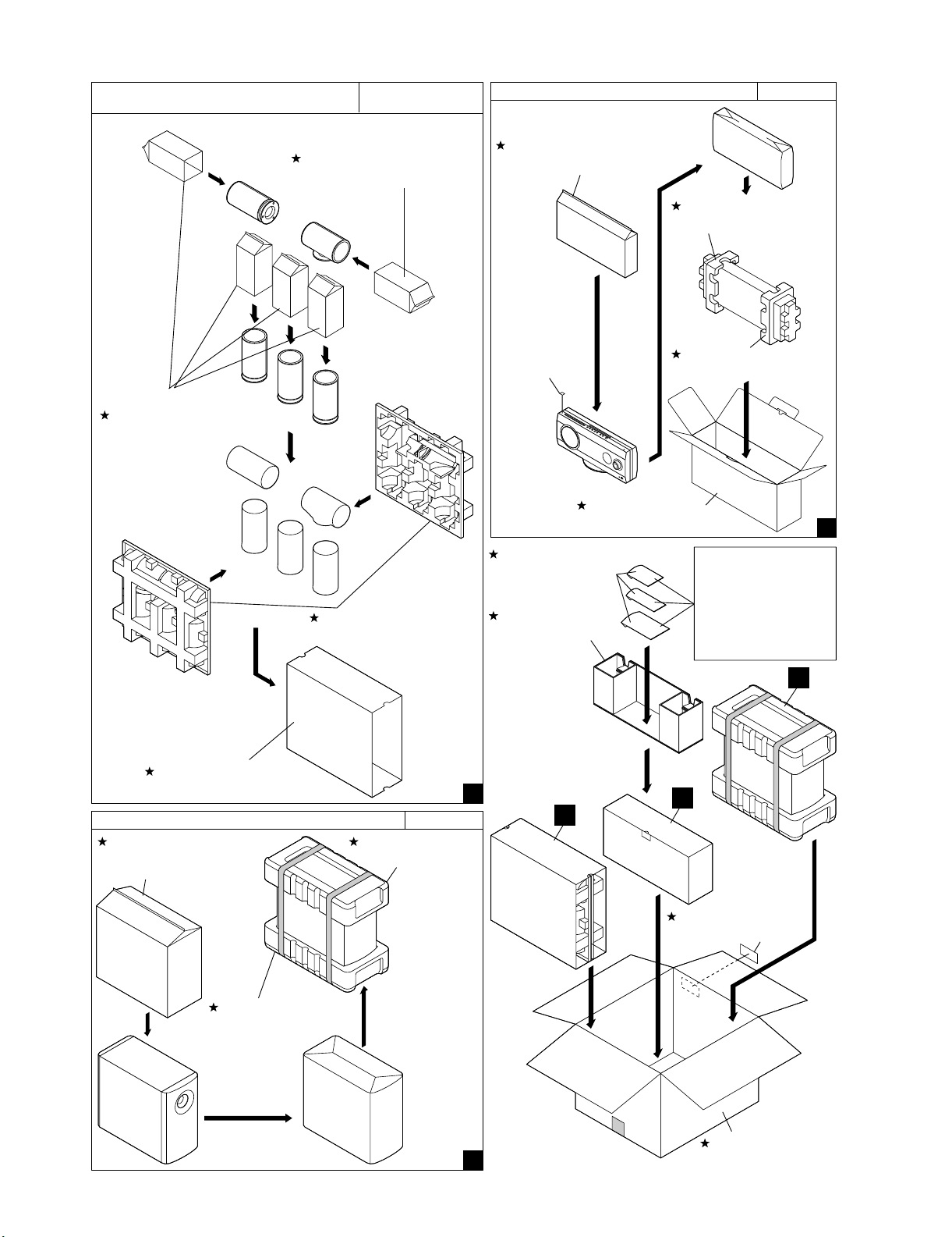
HT-X1
[15] ACCESSORIES/PACKING PARTS
FRONT/CENTER/SURROUND SPEAKER
SSAKHA027SJZZ
Polyethylene Bag,Speaker
SSAKHA026SJZZ
Polyethylene Bag,Speaker
FRONT
FRONT
FRONT
FRONT
FRONT
SPAKAA054SJZZ
Packing Add., Front/Rear
CP-X1F/CP-X1C/
CP-X1S
UNIT
SSAKHA025SJZZ
Polyethylene Bag,Unit
Label, DVD
SPAKCA089SJZZ
Packing Case
SSAKHA023SJZZ
Polyethylene Bag,
Accessories
SPAKPA012SJZZ
Packing Add.
HT-X1
B
O
TTOM
REAR
SPAKAA052SJZZ
Packing Add., Left
TOP
FRONT
SPAKAA053SJZZ
Packing Add., Right
AM/FM Loop Antenna
Operation Manual
Quick Guide
Remote Control
Cable,Video
System Cable
AC Power Supply Cord
A
SPAKSA016SJZZ
Packing Case
SUB WOOFER UNIT
SSAKHA028SJZZ
Polyethylene Bag,
Speaker
TOP
SIDE
SPAKAA057SJZZ
Packing Add., Bottom
BOTTOM
HT-X1
SPAKAA056SJZZ
Packing Add., Top
FRONT
C
TOP
FRONT
B
A
SIDE
B
TLABEA109SJZZ
Bar Code Label
22
SPAKCA129AWZZ
C
Packing Case
Page 81

HT-X1
NO. PARTS CODE
PRICE
RANK
NEW
MARK
PAR T
RANK
DESCRIPTION
[15] ACCESSORIES/PACKING PARTS
SPAKCA089SJZZ AN Packing Case
TINSSA001SJZZ
!
QACCU0003SJ00 AH AC Power Supply Cord
QANTL0008SJZZ AG AM Loop Antenna
QANTWA001SJZZ AF FM Antenna
QCNWGA019SJZZ System Cable
RRMCGA027SJZZ AQ Remote Control
SPAKAA052SJZZ AE Packing Add.
SPAKAA053SJZZ AE Packing Add.
SPAKPA012SJZZ AG Packing Add.
TINSEA050SJZZ AF Operation Manual
SSAKHA023SJZZ AC Polyethylene Bag,Accessories
TINSEA051SJZZ AE Quick Guide
SSAKHA025SJZZ AC Polyethylene Bag
TCAUZA010SJZZ AD Sheet,Guide
QCNWGA008SJZZ AX Speaker Code
QCNWGA004SJZZ AL Cable,Video
HDECPA003SJZZ AC Label,Button Name
TLABZA068SJZZ Label,Feature
SSAKHA028SJZZ Polyethylene Bag
SPAKAA056SJZZ Packing Add.
SPAKAA057SJZZ Packing Add.
TLABEA109SJZZ Label,Bar Code
SPAKSA016SJZZ Packing Case
SPAKAA054SJZZ Packing Add.
SSAKHA026SJZZ Polyethylene Bag
SSAKHA027SJZZ Polyethylene Bag
[16] P.W.B. ASSEMBLY (Not Replacement Item)
PWB-A DUNTKV550SJ03 - Amp./Power 1/Power 2 [PWB-A1~3] (Combined Ass'y)
!
PWB-B DUNTKV549SJ03 - Display/Main/LED/Switch/Headphones/Tuner [PWB-B1~6
[17] OTHER SERVICE PARTS
UDSKA0004AFZZ AZ CD Pickup Lens Cleaner
23
Page 82

HT-X1
INDEX
INDEX
PARTS CODE No.
[ C ]
CCABAA020SJ02 13-201
CCABBA014SJ03 13-202
CCABCA020SJ02 13-203
CMECBA004SJ01 13-204 BP
[ D ]
DCEKDV524SJ03 13-218
DUNTKV549SJ03 16-PWB-B DUNTKV550SJ03 16-PWB-A -
[ G ]
GBOXSA012SJSW 14-101 BE
GCABBA014SJSA 13-202- 1 AR
GCOVAA022SJSA 13-201- 2 AC
GCOVAA030SJSA 13-201- 3 AC
GDAI-A001SJSA 13-205 AH
GDORFA005SJSA 13-206 AL
GITARA032SJSA 14-121 AQ
GWAKPA011SJ01 14-125 AS
GWAKPA012SJSA 14-128 AG
[ H ]
HDECPA002SJZZ 13-213 AC
HDECPA003SJZZ 15- AC
HDECQA062SJSA 13-201- 4 AH
HDECQA064SJSA 13-201- 5 AF
HDECQA065SJSA 13-201- 6 AE
HDECQA066SJSA 13-201- 7 AE
HPNLSA014SJSA 14-124 AK
[ J ]
JKNBKA005SJSA 13-201- 8 AD
JKNBZA032SJSA 13-207 AF
[ K ]
KMECZA004SJZZ 13-204- 1 BD
KRPLEA001SJZZ 13-204- 2 BH
[ L ]
LANGKA041SJFW 14-102 AD
LANGKA042SJ01 14-103 AQ
LANGKA043SJFW 14-104 AK
LANGKA044SJFW 14-105 AC
LANGKA045SJFW 14-106 AE
LANGKA046SJFW 14-107 AG
LANGKA060SJFW 14-108 AL
LANGKA061SJFW 14-109 AD
LANGKA062SJFW 14-110 AE
LANGKA065SJZZ 13-203- 3 AB
LANGKA066SJZZ 13-201- 9 AE
LANGKA092SJFW 13-203- 2
LHLDW1001SJZZ 13-208 AD
" 14-113 AD
LHLDZA039SJZZ 13-209 AB
LHLDZA040SJZZ 13-210 AC
LX-JZA005SJFN 14-801 AB
LX-JZA007SJZZ 13-610 AC
LX-JZA009SJFN 14-806 AB
LX-JZA010SJFN 13-611 AB
LX-JZA011SJFN 13-607 AB
" 14-802 AB
LX-WZA003SJF9 14-803 AB
[ M ]
MSPRDA011SJFW 13-203- 6 AC
MSPRKA001SJFW 14-129 AC
MSPRKA005SJFJ 14-111 AB
[ N ]
NFANPA002SJSA 14-114 AD
[ P ]
PCOVZA006SJZZ 13-201-10 AC
PCOVZA008SJZZ 13-202- 2 AD
PCUSGA010SJZZ 13-203- 7 AB
PCUSGA012SJZZ 13-211 AB
PCUSGA022SJZZ 13-212 AB
PCUSGA024SJSA 14-126 AC
PCUSGA025SJSA 14-127 AC
PCUSGA026SJZZ 13-204- 3 AC
PDUC-A009SJSA 14-123 AG
PRDARA022SJZZ 14-118 AW
PRDARA023SJZZ 14-119 AD
PRDARA024SJZZ 14-117 AC
PRDARA028SJZZ 13-215 AG
PRDARA036SJFW 13-217 AC
PSHEFA013SJZZ 13-201-12
PRICE
RANK
NEW
MARK
PART
RANK
PARTS CODE No.
PSHEPA005SJZZ 13-201-11 AF
PSHEZA003SJZZ 14-120 AC
PSLDCA001SJZZ 13-201-13 AD
PSLDMA007SJZZ 13-203- 4 AG
PSLDMA008SJZZ 13-203- 5 AG
PSLDMA009SJZZ 13-202- 3 AG
PSLDMA012SJZZ 13-202- 4 AH
PSPAGA003SJZZ 14-122 AD
[ Q ]
QACCU0003SJ00 15-2 AH
QANTL0008SJZZ 15- AG
QANTWA001SJZZ 15- AF
QCNCM004BSJZZ 12-CNP707 AB
QCNCM004DSJZZ 12-CNP205 AB
" 12-CNP301 AB
QCNCM004FSJZZ 12-CNP609 AB
QCNCM004GSJZZ 12-CNP302
QCNCM004MSJZZ 12-CNP702 AC
QCNCM004NSJZZ 12-CNP704 AC
QCNCM017BSJZZ 12-CNP201 AD
" 12-CNP203 AD
QCNCM017CSJZZ 12-CNP202 AC
QCNCM052CSJZZ 12-CNP206 AB
QCNCM998DAFZZ 12-CNP204 AB
QCNCM998NAFZZ 12-CNP401 AG
QCNCM999EAFZZ 12-CNP402A AG
QCNCM999JAFZZ 12-CNP402B AC
QCNCMA013SJ07 12-CNP705 AC
QCNCWA028SJZZ 12-S102A AG
" 12-S102B AG
QCNCWA030SJZZ 12-S101A AG
" 12-S101B AG
QCNWGA004SJZZ 15- AL
QCNWGA008SJZZ 15- AX
QCNWGA019SJZZ 15QCNWNA032SJZZ 12-CNP706 AE
QCNWNA188SJZZ 12-BI501 AK
QCNWNA189SJZZ 12-BI502 AH
QCNWNA190SJZZ 12-BI503 AK
QCNWNA191SJZZ 12-BI506 AG
QCNWNA192SJZZ 12-CNW508A/ AF
QCNWNA193SJZZ 12-BI203 AE
QCNWNA194SJZZ 12-BI401 AK
QCNWNA195SJZZ 12-BI402 AK
QCNWNA196SJZZ 12-BI205 AD
QCNWNA197SJZZ 12-BI302 AE
QCNWNA198SJZZ 12-CNW609 AE
QCNWNA199SJZZ 12-CNW705 AE
QCNWNA200SJZZ 12-CNW707 AC
QCNWNA202SJZZ 13-222
QCNWNA212SJZZ 12-CNW702 AG
QCNWNA213SJZZ 12-CNW704 AG
QCNWNA216SJZZ 13-223
QCNWNA226SJZZ 12-CFW6A AC
QCNWNA227SJZZ 12-CFW4 AC
" 12-CFW5 AC
QCNWNA228SJZZ 12-CFW6 AC
" 12-CFW9 AC
QCNWNA229SJZZ 12-CFW2 AC
QCNWNA230SJZZ 12-CFW1 AB
QCNWNA231SJZZ 12-CFW3 AB
QCNWNA232SJZZ 12-CNW703 AE
QCNWNA311SJZZ 12-CNW301
QFS-D202BSJNI 12-F201 AB
QFS-D632BSJNI 12-F101 AC
" 12-F102 AC
QFSHD1013CEZZ 14-112 AB
QJAKMA002SJZZ 12-JK1 AE
QSOCA0214AWZZ 12-SO202 AD
QSOCJ0003SJZZ 12-S504 AG
QSOCJA005SJZZ 12-S501 AE
QSOCZA006SJZZ 12-S505
QSW-K0002SJZZ 12-SW701 AC
" 12-SW702 AC
" 12-SW703 AC
" 12-SW704 AC
" 12-SW705 AC
" 12-SW706 AC
" 12-SW707 AC
" 12-SW708 AC
PRICE
RANK
NEW
MARK
PAR T
RANK
24
Page 83

PARTS CODE No.
QSW-ZA002SJZZ 12-SW700 AF
QTANAA005SJZZ 12-SO401 AF
QTANCA001SJZZ 12-SO301 AD
QTANCA002SJZZ 12-SO302 AC
[ R ]
RBLN-0001SJZZ 6-L301 AE
RBLN-A001SJZZ 6-L506 AB
"6-L507AB
"6-L508AB
"6-L509AB
"6-L511AB
RC-EZD106AF1C 10-C501 AB
" 10-C505 AB
" 10-C506 AB
" 10-C510 AB
" 10-C513 AB
" 10-C517 AB
" 10-C518 AB
" 10-C522 AB
" 10-C525 AB
" 10-C529 AB
" 10-C530 AB
" 10-C534 AB
" 10-C633 AB
" 10-C634 AB
RC-EZD107AF1A 10-C709 AB
" 10-C718 AB
RC-EZD107AF1C 10-C639 AC
" 10-C640 AC
RC-EZD107AF1E 10-C584 AD
" 10-C599 AD
RC-EZD225AF1H 10-C547 AB
RC-EZD226AF1E 10-C594 AB
" 10-C596 AB
" 10-C598 AB
RC-EZD227AF1A 10-C706 AC
RC-EZD227AF1C 10-C665 AB
RC-EZD336AF1C 10-C712 AB
RC-EZD476AF1C 10-C394 AC
" 10-C503 AC
" 10-C515 AC
" 10-C527 AC
" 10-C545 AC
" 10-C590 AC
" 10-C716 AC
" 10-C510A AC
" 10-C510B AC
" 10-C510C AC
" 10-C667A AC
RC-EZD477AF1C 10-C585 AB
" 10-C667 AB
RC-GZA105AF1H 10-C107 AB
" 10-C109 AB
" 10-C112 AB
" 10-C120 AB
" 10-C124 AB
" 10-C133 AB
" 10-C168 AB
" 10-C358 AB
" 10-C367 AB
" 10-C368 AB
" 10-C370 AB
" 10-C371 AB
" 10-C372 AB
" 10-C393 AB
RC-GZA106AF1C 10-C352 AB
" 10-C364 AB
" 10-C380 AB
" 10-C401 AB
" 10-C402 AB
" 10-C405 AB
" 10-C413 AB
" 10-C414 AB
" 10-C422 AB
" 10-C425 AB
" 10-C479 AB
" 10-C488 AB
" 10-C489 AB
" 10-C497 AB
" 10-C540 AB
" 10-C541 AB
" 10-C544 AB
PRICE
RANK
NEW
MARK
PART
RANK
PARTS CODE No.
" 10-C549 AB
" 10-C564 AB
" 10-C571 AB
" 10-C572 AB
" 10-C801 AB
" 10-C802 AB
" 10-C810 AB
" 10-C811 AB
" 10-C812 AB
" 10-C813 AB
" 10-C901 AB
" 10-C479A AB
" 10-C500A AB
" 10-C500B AB
" 10-C500C AB
" 10-C529A AB
" 10-C529B AB
" 10-C529C AB
" 10-C582B AB
" 10-C582C AB
" 10-C582D AB
" 10-C582E AB
RC-GZA106AF1H 10-C102 AB
" 10-C104 AB
" 10-C105 AB
" 10-C106 AB
" 10-C114 AB
" 10-C116 AB
" 10-C117 AB
" 10-C118 AB
" 10-C170 AB
" 10-C173 AB
" 10-C174 AB
" 10-C176 AB
RC-GZA107AF1A 10-C396 AB
" 10-C398 AB
RC-GZA107AF1C 10-C325 AB
" 10-C348 AB
" 10-C470 AB
" 10-C555 AB
RC-GZA107AF1H 10-C210 AC
" 10-C215 AC
RC-GZA225AF1C 10-C151 AC
" 10-C557 AC
" 10-C565 AC
RC-GZA225AF1H 10-C357 AB
" 10-C561 AB
" 10-C569 AB
RC-GZA227AF1A 10-C587 AB
RC-GZA227AF1E 10-C218 AB
RC-GZA227AF1H 10-C213 AE
RC-GZA335AF1C 10-C463 AB
RC-GZA335AF1H 10-C362 AB
RC-GZA336AF1C 10-C556 AB
RC-GZA475AF1H 10-C562 AB
" 10-C570 AB
RC-GZA476AF1C 10-C226 AB
" 10-C391 AB
" 10-C412 AB
" 10-C416 AB
" 10-C417 AB
" 10-C478 AB
" 10-C481 AB
" 10-C580 AB
" 10-C591 AB
" 10-C720 AB
" 10-C902 AB
" 10-C402A AB
" 10-C422A AB
" 10-C478A AB
" 10-C497A AB
" 10-C543A AB
" 10-C582A AB
RC-GZA476AF1E 10-C216 AB
" 10-C256 AB
" 10-C537 AB
" 10-C543 AB
" 10-C589 AB
" 10-C216A AB
RC-GZA476AF1H 10-C108 AB
" 10-C111 AB
" 10-C119 AB
PRICE
RANK
NEW
MARK
HT-X1
PAR T
RANK
25
Page 84
HT-X1
PARTS CODE No.
" 10-C123 AB
" 10-C167 AB
" 10-C172 AB
" 10-C211 AB
" 10-C212 AB
" 10-C465 AB
" 10-C806 AB
" 10-C809 AB
RC-GZA476AF1J 10-C214 AC
RC-GZV228AF1C 10-C232 AG
RC-GZW338AF1E 10-C224 AG
RC-GZW478AF1H 10-C128 AH
" 10-C129 AH
RC-GZW688AF1E 10-C207 AH
RCILAA002SJZZ 5-T302 AC
RCILBA006SJZZ 5-T306 AC
RCILCA001SJZZ 6-L501 AD
RCILIA002SJZZ 5-T351 AC
RCILZA004SJZZ 6-LF201 AD
RCORF0010SJZZ 6-L510 AB
" 6-L5A1 AB
RCORFA008SJZZ 6-L513 AB
" 6-L514 AB
" 6-L513A AB
" 6-L513B AB
RC-QZA104AFYJ 10-C559 AC
" 10-C567 AC
RCRM-0007SJZZ 9-X351 AG
RCRM-0008SJZZ 9-X702 AG
RCRSP0006SJZZ 9-X352 AF
RCRSPA007SJZZ 9-X701 AE
RFILA0003SJZZ 4-CF352 AF
RFILF0003AWZZ 4-CF351 AK
RFILFA001SJZZ 4-CF302 AE
" 4-CF303 AE
RFILL0001SJZZ 6-L354 AF
RH-IX0058SJZZ 1-IC701 BH
RMOTV0409AFZZ 12-M401 AL
" 12-M402 AL
RRLYD0004SJZZ 12-RLY400 AG
RRLYDA002AWZZ 12-RLY401
" 12-RLY402
" 12-RLY403
RRMCGA027SJZZ 15- AQ
RSP-ZA004SJZZ 14-SP1 AS
RTRNPA039SJZZ 5-T201
RTRNPA040SJZZ 5-T202
RTUNSA003SJZZ 1-IC301 AS
RVR-M0026AWZZ 7-VR351 AC
[ S ]
SPAKAA052SJZZ 15- AE
SPAKAA053SJZZ 15- AE
SPAKAA054SJZZ 15SPAKAA056SJZZ 15SPAKAA057SJZZ 15SPAKCA089SJZZ 15- AN
SPAKPA012SJZZ 15- AG
SPAKSA016SJZZ 15SSAKHA023SJZZ 15- AC
SSAKHA025SJZZ 15- AC
SSAKHA026SJZZ 15SSAKHA027SJZZ 15SSAKHA028SJZZ 15-
[ T ]
TCAUZA010SJZZ 15- AD
TINSEA050SJZZ 15- AF
TINSEA051SJZZ 15- AE
TINSSA001SJZZ 15TLABEA109SJZZ 15TLABSA005SJZZ 13-221 AB
TLABZA068SJZZ 15TSPC-A058SJZZ 13-214
TSPC-A089SJZZ 14-116
[ U ]
UDSKA0004AFZZ 17- AZ
[ V ]
VCCCCY1HH102J 10-C502 AA
" 10-C507 AA
" 10-C514 AA
" 10-C519 AA
" 10-C526 AA
" 10-C531 AA
PRICE
RANK
NEW
MARK
PART
RANK
PARTS CODE No.
" 10-C574 AA
VCCCCY1HH120J 10-C381 AA
VCCCCY1HH150J 10-C382 AA
VCCCCY1HH151J 10-C509 AA
VCCCCY1HH220J 10-C511 AA
" 10-C512 AA
" 10-C523 AA
" 10-C524 AA
" 10-C535 AA
" 10-C536 AA
" 10-C703 AA
" 10-C704 AA
VCCCCY1HH221J 10-C233 AA
" 10-C234 AA
" 10-C235 AA
" 10-C236 AA
" 10-C237 AA
" 10-C238 AA
" 10-C548 AA
" 10-C552 AA
" 10-C553 AA
" 10-C554 AA
VCCCCY1HH330J 10-C637 AA
" 10-C638 AA
VCCCCY1HH331J 10-C576 AA
" 10-C577 AA
VCCCCY1HH470J 10-C403 AA
" 10-C404 AA
" 10-C420 AA
" 10-C421 AA
" 10-C431 AA
" 10-C504 AA
" 10-C516 AA
" 10-C521 AA
" 10-C528 AA
" 10-C533 AA
" 10-C532A AA
" 10-C532B AA
VCCCPA1HH120J 10-C330 AA
VCCSCY1HL220J 10-C355 AD
VCCSCY1HL330J 10-C343 AD
" 10-C344 AD
VCCSCY1HL560J 10-C369 AD
VCCUPA1HJ270J 10-C334 AA
VCFYFA1HA104J 10-C426 AC
" 10-C435 AC
" 10-C484 AC
" 10-C485 AC
" 10-C490 AC
" 10-C546 AC
" 10-C803 AC
VCFYFA1HA473J 10-C225 AB
" 10-C227 AB
VCKYCY1EF103Z 10-C376 AA
VCKYCY1EF123Z 10-C301 AA
VCKYCY1EF223Z 10-C329 AB
" 10-C341 AB
" 10-C345 AB
" 10-C346 AB
" 10-C347 AB
" 10-C350 AB
" 10-C351 AB
" 10-C353 AB
" 10-C354 AB
" 10-C360 AB
" 10-C361 AB
" 10-C363 AB
" 10-C365 AB
" 10-C383 AB
" 10-C387 AB
" 10-C395 AB
" 10-C397 AB
VCKYCY1EF473Z 10-C331 AB
" 10-C538 AB
" 10-C672 AB
VCKYCY1HB101K 10-C708 AB
" 10-C719 AB
VCKYCY1HB102K 10-C302 AA
" 10-C349 AA
" 10-C356 AA
" 10-C366 AA
" 10-C384 AA
PRICE
RANK
NEW
MARK
PART
RANK
26
Page 85

PARTS CODE No.
" 10-C392 AA
" 10-C714 AA
" 10-C715 AA
VCKYCY1HB103K 10-C713 AA
VCKYCY1HB104K 10-C014 AD
" 10-C015 AD
" 10-C101 AD
" 10-C103 AD
" 10-C113 AD
" 10-C115 AD
" 10-C132 AD
" 10-C175 AD
" 10-C177 AD
" 10-C573 AD
" 10-C581 AD
" 10-C586 AD
" 10-C701 AD
" 10-C702 AD
" 10-C705 AD
" 10-C707 AD
" 10-C711 AD
" 10-C512A AD
" 10-C512B AD
" 10-C512C AD
" 10-C586A AD
VCKYCY1HB151K 10-C110 AA
" 10-C121 AA
" 10-C125 AA
" 10-C126 AA
" 10-C166 AA
" 10-C169 AA
" 10-C201 AA
" 10-C202 AA
" 10-C203 AA
" 10-C204 AA
" 10-C205 AA
" 10-C498 AA
" 10-C206B AA
VCKYCY1HB153K 10-C550 AA
VCKYCY1HB221K 10-C451 AA
" 10-C453 AA
VCKYCY1HB222K 10-C136 AA
" 10-C137 AA
" 10-C575 AA
" 10-C5B4 AA
" 10-C820 AA
" 10-C821 AA
" 10-C904 AA
" 10-C599A AA
" 10-C599B AA
VCKYCY1HB223K 10-C641 AA
VCKYCY1HB271K 10-C599C AA
" 10-C599D AA
VCKYCY1HB272K 10-C560 AA
" 10-C568 AA
VCKYCY1HB332K 10-C539 AA
VCKYCY1HB472K 10-C706A AA
VCKYCY1HB473K 10-C388 AB
" 10-C588 AB
" 10-C592 AB
VCKYCY1HB561K 10-C335 AA
VCKYCY1HB681K 10-C450 AA
VCKYCY1HF104Z 10-C411 AB
" 10-C415 AB
" 10-C494 AB
VCKYCY1HF223Z 10-C814 AA
" 10-C815 AA
" 10-C816 AA
" 10-C817 AA
" 10-C818 AA
" 10-C819 AA
VCKYCY1HF473Z 10-C710 AB
" 10-C717 AB
VCKYPA1HB104K 10-C127 AC
" 10-C130 AC
" 10-C131 AC
" 10-C134 AC
" 10-C153 AC
" 10-C438 AC
" 10-C442 AC
" 10-C443 AC
" 10-C444 AC
PRICE
RANK
NEW
MARK
PART
RANK
PARTS CODE No.
" 10-C446 AC
" 10-C452 AC
" 10-C558 AC
" 10-C566 AC
" 10-C5B3 AC
VCKYPA1HB222K 10-C464 AA
" 10-C5A1 AA
" 10-C5A4 AA
" 10-C5A5 AA
" 10-C5A6 AA
" 10-C5A7 AA
" 10-C5A8 AA
" 10-C5A9 AA
" 10-C5B1 AA
" 10-C5B2 AA
VCKYPA1HB223K 10-C016 AB
" 10-C188 AB
" 10-C189 AB
" 10-C190 AB
" 10-C191 AB
" 10-C192 AB
" 10-C193 AB
" 10-C194 AB
" 10-C195 AB
" 10-C196 AB
" 10-C197 AB
" 10-C198 AB
" 10-C199 AB
VCKYPA1HB331K 10-C378 AA
" 10-C386 AA
VCKYPA1HB472K 10-C433 AB
" 10-C440 AB
" 10-C445 AB
" 10-C449 AB
" 10-C495 AB
" 10-C496 AB
" 10-C822 AB
" 10-C823 AB
" 10-C824 AB
" 10-C825 AB
" 10-C826 AB
" 10-C827 AB
VCKYPA1HF102Z 10-C903 AA
VCKYPA1HF103Z 10-C385 AB
VCKYPA1HF104Z 10-C206 AB
" 10-C208 AB
" 10-C209 AB
" 10-C429 AB
" 10-C434 AB
" 10-C206A AB
VCKYPA1HF223Z 10-C219 AB
" 10-C324 AB
" 10-C332 AB
" 10-C337 AB
" 10-C399 AB
VCKYPA1HF473Z 10-C217 AB
" 10-C228 AB
" 10-C229 AB
VCQYKA1JM224J 10-C670 AC
VCTYPA1CX183K 10-C373 AA
" 10-C374 AA
VHCSVC348S/-1 8-VD301 AK
VHD1N4004//-1 3-D209 AB
" 3-D210 AB
" 3-D211 AB
" 3-D212 AB
" 3-D216 AB
" 3-D217 AB
" 3-D218 AB
" 3-D219 AB
" 3-D220 AB
" 3-D221 AB
" 3-D424 AB
" 3-D425 AB
" 3-D426 AB
" 3-D427 AB
" 3-D505 AB
" 3-D506 AB
" 3-D507 AB
" 3-D511 AB
" 3-D701 AB
" 3-D706 AB
PRICE
RANK
NEW
MARK
HT-X1
PAR T
RANK
27
Page 86

HT-X1
PARTS CODE No.
" 3-D708 AB
" 3-D427A AB
VHD1N4148//-1 3-D102 AA
" 3-D301 AA
" 3-D302 AA
" 3-D303 AA
" 3-D304 AA
" 3-D308 AA
" 3-D410 AA
" 3-D411 AA
" 3-D416 AA
" 3-D417 AA
" 3-D418 AA
" 3-D419 AA
" 3-D420 AA
" 3-D421 AA
" 3-D422 AA
" 3-D429 AA
" 3-D431 AA
" 3-D432 AA
" 3-D433 AA
" 3-D434 AA
" 3-D435 AA
" 3-D436 AA
" 3-D437 AA
" 3-D440 AA
" 3-D441 AA
" 3-D442 AA
" 3-D443 AA
" 3-D452 AA
" 3-D453 AA
" 3-D454 AA
" 3-D455 AA
" 3-D456 AA
" 3-D457 AA
" 3-D458 AA
" 3-D459 AA
" 3-D509 AA
" 3-D702 AA
" 3-D703 AA
" 3-D704 AA
" 3-D705 AA
" 3-D707 AA
" 3-ZD424 AA
VHD1N4148W/-1 3-D503 AB
" 3-D504 AB
" 3-D512 AB
" 3-D706A AB
" 3-D706B AB
VHD1N5402M/-1 3-D205 AE
" 3-D206 AE
" 3-D207 AE
" 3-D208 AE
VHD1N5822//-1 3-D508 AD
VHDGBJ10GM/-1 3-D101 AH
VHEDZH03C3+-1 3-ZD425 AB
" 3-ZD701 AB
VHEDZH05C2+-1 3-ZD351 AB
VHEDZH06C2+-1 3-ZD202 AB
VHEDZH09C1+-1 3-ZD423 AB
VHEDZH1602+-1 3-ZD101 AB
" 3-ZD102 AB
VHEDZH3001+-1 3-ZD201 AB
VHIAN78L05/-1 1-IC203 AE
VHICD4053M+-1 1-IC507 AF
VHIKIA7805API 1-IC201 AF
" 1-IC502 AF
" 1-IC511 AF
VHIKIA7812API 1-IC202 AE
" 1-IC501 AE
VHILA1832S/-1 1-IC303 AN
VHILC72131/-1 1-IC302 AP
VHILC75341M-1 1-IC505 AM
VHILM2576T/-1 1-IC503 AR
VHILM4732TA-1 1-IC101 AY
" 1-IC102 AY
" 1-IC103 AY
VHINJM14558-1 1-IC506 AF
" 1-IC508 AF
" 1-IC509 AF
" 1-IC512 AF
VHINJM4558D-1 1-IC104 AH
PRICE
RANK
NEW
MARK
PART
RANK
PARTS CODE No.
" 1-IC404 AH
" 1-IC405 AH
" 1-IC406 AH
" 1-IC504 AH
" 1-IC510 AH
VHITCD4094B-1 1-IC407 AE
VHLGP1UD261-1 12-RX701 AK
" 12-RX702 AK
VHPBFRX1001-1 12-S503 AM
VHPLPBB73V1-1 3-LED702 AF
VP-DH100K0000 6-L503 AB
"6-L504AB
VP-DH101K0000 6-L351 AB
"6-L352AB
VP-DH102K0000 6-L353 AB
VP-DH2R2K0000 6-L342 AB
"6-L502AB
"6-L706AB
VP-DHR82K0000 6-L701 AE
"6-L703AE
"6-L704AE
"6-L705AE
VRD-RT2HDR20J 11-R914
" 11-R917
" 11-R923
" 11-R925
" 11-R928
" 11-R934
VRD-ST2CD100J 11-R207 AA
VRD-ST2CD101J 11-R618 AA
" 11-R627 AA
" 11-R629 AA
" 11-R630 AA
" 11-R836 AA
VRD-ST2CD102J 11-R206 AA
" 11-R489 AA
" 11-R490 AA
" 11-R491 AA
" 11-R492 AA
" 11-R493 AA
" 11-R494 AA
" 11-R568 AA
" 11-R592 AA
" 11-R703 AA
" 11-R705 AA
" 11-R708 AA
" 11-R709 AA
" 11-R710 AA
" 11-R712 AA
" 11-R713 AA
" 11-R714 AA
" 11-R715 AA
" 11-R718 AA
" 11-R720 AA
" 11-R721 AA
" 11-R722 AA
" 11-R723 AA
" 11-R724 AA
" 11-R725 AA
" 11-R727 AA
" 11-R728 AA
" 11-R729 AA
" 11-R731 AA
" 11-R732 AA
" 11-R736 AA
" 11-R738 AA
" 11-R739 AA
" 11-R747 AA
" 11-R748 AA
" 11-R749 AA
" 11-R756 AA
" 11-R761 AA
" 11-R767 AA
" 11-R770 AA
" 11-R791 AA
" 11-R793 AA
" 11-R869 AA
" 11-R869A AA
VRD-ST2CD103J 11-R154 AA
" 11-R210 AA
" 11-R376 AA
" 11-R586 AA
PRICE
RANK
NEW
MARK
PART
RANK
28
Page 87

PARTS CODE No.
" 11-R590 AA
" 11-R704 AA
" 11-R706 AA
" 11-R730 AA
" 11-R735 AA
" 11-R745 AA
" 11-R754 AA
" 11-R797 AA
" 11-R475A AA
" 11-R735A AA
" 11-R735B AA
VRD-ST2CD104J 11-R589 AA
" 11-R591 AA
" 11-R764 AA
" 11-R831 AA
VRD-ST2CD121J 11-R593 AA
VRD-ST2CD123J 11-R203 AA
VRD-ST2CD153J 11-R405 AA
" 11-R411 AA
" 11-R435 AA
" 11-R444 AA
" 11-R458 AA
" 11-R465 AA
VRD-ST2CD181J 11-R343 AA
VRD-ST2CD183J 11-R112 AA
" 11-R113 AA
" 11-R122 AA
VRD-ST2CD222J 11-R366 AA
" 11-R510C AA
" 11-R510D AA
VRD-ST2CD223J 11-R864 AA
" 11-R943 AA
" 11-R864A AA
VRD-ST2CD271J 11-R153 AA
VRD-ST2CD272J 11-R216 AA
" 11-R614 AA
VRD-ST2CD273J 11-R616 AA
" 11-R409A AA
" 11-R436A AA
" 11-R461A AA
VRD-ST2CD331J 11-R204 AA
" 11-R205 AA
VRD-ST2CD332J 11-R401 AA
" 11-R402 AA
" 11-R437 AA
" 11-R440 AA
" 11-R463 AA
" 11-R467 AA
" 11-R763 AA
" 11-R862 AA
" 11-R868 AA
" 11-R895 AA
" 11-R897 AA
" 11-R899 AA
" 11-R901 AA
" 11-R510B AA
" 11-R862A AA
" 11-R868A AA
VRD-ST2CD334J 11-R460 AA
VRD-ST2CD390J 11-R909 AA
VRD-ST2CD392J 11-R552 AA
VRD-ST2CD472J 11-R861 AA
VRD-ST2CD473J 11-R208 AA
" 11-R218 AA
" 11-R395 AA
" 11-R553 AA
VRD-ST2CD474J 11-R865 AA
" 11-R865A AA
VRD-ST2CD4R7J 11-R190 AA
" 11-R191 AA
" 11-R192 AA
" 11-R193 AA
" 11-R194 AA
" 11-R195 AA
VRD-ST2CD560J 11-R594 AA
VRD-ST2CD562J 11-R336 AA
" 11-R377 AA
" 11-R385 AA
" 11-R387 AA
VRD-ST2CD563J 11-R471 AA
VRD-ST2CD681J 11-R942 AA
VRD-ST2CD682J 11-R384 AA
PRICE
RANK
NEW
MARK
PART
RANK
PARTS CODE No.
" 11-R945 AA
VRD-ST2CD820J 11-R201 AA
" 11-R202 AA
" 11-R775 AA
VRD-ST2CD821J 11-R860 AA
VRD-ST2EE100J 11-R399 AA
" 11-R952 AA
" 11-R957 AA
VRD-ST2EE102J 11-R101 AA
" 11-R102 AA
" 11-R103 AA
" 11-R155 AA
" 11-R181 AA
VRD-ST2EE121J 11-R983 AA
" 11-R984 AA
VRD-ST2EE221J 11-R787 AA
VRD-ST2EE330J 11-R867 AA
" 11-R867A AA
VRD-ST2EE331J 11-R382 AA
" 11-R386 AA
VRD-ST2EE391J 11-R391 AA
" 11-R392 AA
VRD-ST2EE470J 11-R760A AA
" 11-R760B AA
VRD-ST2EE4R7J 11-R834 AA
" 11-R835 AA
" 11-R841 AA
" 11-R842 AA
" 11-R843 AA
" 11-R850 AA
VRD-ST2HD475J 11-R985 AA
VRD-ST3LD0R1J 11-R166
VRS-CY1JB000J 11-JP2 AA
" 11-JP3 AA
" 11-JP4 AA
" 11-JP5 AA
" 11-JP6 AA
" 11-R197 AA
" 11-R350 AA
" 11-R356 AA
" 11-R361 AA
" 11-R362 AA
" 11-R581 AA
" 11-R585 AA
" 11-R707 AA
" 11-R746 AA
" 11-R976 AA
" 11-JB101 AA
" 11-JB103 AA
" 11-JR401 AA
VRS-CY1JB100J 11-R505 AA
" 11-R510 AA
" 11-R517 AA
" 11-R522 AA
" 11-R529 AA
" 11-R534 AA
VRS-CY1JB101J 11-R406 AA
" 11-R412 AA
" 11-R434 AA
" 11-R443 AA
" 11-R457 AA
" 11-R975 AA
VRS-CY1JB102J 11-R76 AA
" 11-R104 AA
" 11-R105 AA
" 11-R115 AA
" 11-R172 AA
" 11-R352 AA
" 11-R371 AA
" 11-R372 AA
" 11-R373 AA
" 11-R374 AA
" 11-R393 AA
" 11-R414 AA
" 11-R425 AA
" 11-R426 AA
" 11-R447 AA
" 11-R450 AA
" 11-R468 AA
" 11-R559 AA
" 11-R561 AA
" 11-R566 AA
PRICE
RANK
NEW
MARK
HT-X1
PAR T
RANK
29
Page 88
HT-X1
PARTS CODE No.
" 11-R567 AA
" 11-R595 AA
" 11-R596 AA
" 11-R617 AA
" 11-R619 AA
" 11-R700 AA
" 11-R701 AA
" 11-R716 AA
" 11-R737 AA
" 11-R740 AA
" 11-R750 AA
" 11-R751 AA
" 11-R755 AA
" 11-R762 AA
" 11-R769 AA
" 11-R776 AA
" 11-R972 AA
" 11-R973 AA
" 11-R974 AA
" 11-R595A AA
VRS-CY1JB103D 11-R159 AA
" 11-R170 AA
VRS-CY1JB103J 11-R156 AA
" 11-R198 AA
" 11-R365 AA
" 11-R381 AA
" 11-R423 AA
" 11-R424 AA
" 11-R448 AA
" 11-R449 AA
" 11-R451 AA
" 11-R511 AA
" 11-R512 AA
" 11-R523 AA
" 11-R524 AA
" 11-R535 AA
" 11-R536 AA
" 11-R537 AA
" 11-R541 AA
" 11-R544 AA
" 11-R545 AA
" 11-R554 AA
" 11-R557 AA
" 11-R572 AA
" 11-R577 AA
" 11-R578 AA
" 11-R579 AA
" 11-R604 AA
" 11-R688 AA
" 11-R699 AA
" 11-R702 AA
" 11-R719 AA
" 11-R734 AA
" 11-R742 AA
" 11-R743 AA
" 11-R744 AA
" 11-R768 AA
" 11-R772 AA
" 11-R777 AA
" 11-R778 AA
" 11-R788 AA
" 11-R789 AA
" 11-R790 AA
" 11-R792 AA
" 11-R808 AA
" 11-R863 AA
" 11-R896 AA
" 11-R898 AA
" 11-R900 AA
" 11-R902 AA
" 11-R908 AA
" 11-R946 AA
" 11-R949 AA
" 11-R950 AA
" 11-R951 AA
" 11-R953 AA
" 11-R954 AA
" 11-R955 AA
" 11-R956 AA
" 11-R982 AA
" 11-R863A AA
VRS-CY1JB104J 11-R415 AA
PRICE
RANK
NEW
MARK
PART
RANK
PARTS CODE No.
" 11-R428 AA
" 11-R445 AA
" 11-R452 AA
" 11-R477 AA
" 11-R487 AA
" 11-R542 AA
" 11-R547 AA
" 11-R549 AA
" 11-R550 AA
" 11-R551 AA
" 11-R605 AA
" 11-R608 AA
" 11-R832 AA
" 11-R833 AA
" 11-R838 AA
" 11-R839 AA
" 11-R840 AA
" 11-R870 AA
VRS-CY1JB106J 11-R741 AA
VRS-CY1JB121J 11-R779 AA
VRS-CY1JB122J 11-R171 AA
" 11-R587 AA
" 11-R588 AA
" 11-R765 AA
" 11-R766 AA
" 11-R780 AA
" 11-R781 AA
VRS-CY1JB123J 11-R110 AA
" 11-R111 AA
" 11-R119 AA
" 11-R915 AA
" 11-R918 AA
" 11-R924 AA
" 11-R927 AA
" 11-R931 AA
" 11-R932 AA
VRS-CY1JB124D 11-R157 AA
" 11-R981 AA
VRS-CY1JB124J 11-R509 AA
VRS-CY1JB152J 11-R380 AA
" 11-R548 AA
" 11-R689 AA
" 11-R782 AA
VRS-CY1JB181J 11-R5C1 AA
" 11-R5C2 AA
VRS-CY1JB182J 11-R359 AA
" 11-R961 AA
" 11-R963 AA
" 11-R964 AA
" 11-R967 AA
" 11-R969 AA
" 11-R971 AA
VRS-CY1JB183D 11-R160 AA
" 11-R161 AA
" 11-R162 AA
" 11-R163 AA
" 11-R164 AA
" 11-R165 AA
" 11-R167 AA
" 11-R168 AA
" 11-R977 AA
" 11-R978 AA
" 11-R979 AA
" 11-R980 AA
VRS-CY1JB183J 11-R118 AA
" 11-R121 AA
" 11-R123 AA
" 11-R590B AA
VRS-CY1JB184D 11-R158 AA
" 11-R169 AA
VRS-CY1JB202J 11-R684 AA
VRS-CY1JB221J 11-R546 AA
VRS-CY1JB222J 11-R199 AA
" 11-R379 AA
" 11-R783 AA
VRS-CY1JB223J 11-R564 AA
" 11-R569 AA
" 11-R784 AA
" 11-R785 AA
" 11-R944 AA
VRS-CY1JB271J 11-R353 AA
" 11-R540 AA
PRICE
RANK
NEW
MARK
PART
RANK
30
Page 89

PARTS CODE No.
VRS-CY1JB272J 11-R612 AA
VRS-CY1JB273J 11-R407 AA
" 11-R409 AA
" 11-R436 AA
" 11-R441 AA
" 11-R459 AA
" 11-R461 AA
" 11-R502 AA
" 11-R507 AA
" 11-R514 AA
" 11-R519 AA
" 11-R526 AA
" 11-R531 AA
" 11-R573 AA
" 11-R574 AA
" 11-R575 AA
" 11-R576 AA
" 11-R615 AA
" 11-R866 AA
" 11-R407A AA
" 11-R441A AA
" 11-R459A AA
" 11-R502A AA
" 11-R507A AA
" 11-R514A AA
" 11-R519A AA
" 11-R526A AA
" 11-R531A AA
" 11-R539A AA
" 11-R541A AA
" 11-R542A AA
" 11-R543A AA
" 11-R590A AA
" 11-R590C AA
" 11-R590D AA
" 11-R590E AA
" 11-R615A AA
" 11-R616A AA
" 11-R866A AA
VRS-CY1JB303J 11-R504 AA
" 11-R516 AA
" 11-R521 AA
" 11-R528 AA
" 11-R533 AA
VRS-CY1JB330J 11-R349 AA
VRS-CY1JB331J 11-R346 AA
VRS-CY1JB332J 11-R152 AA
" 11-R355 AA
" 11-R503 AA
" 11-R508 AA
" 11-R515 AA
" 11-R520 AA
" 11-R527 AA
" 11-R532 AA
" 11-R5B1 AA
" 11-R5B2 AA
" 11-R601 AA
" 11-R602 AA
" 11-R941 AA
" 11-R510A AA
VRS-CY1JB333J 11-R408 AA
" 11-R410 AA
" 11-R433 AA
" 11-R442 AA
" 11-R456 AA
VRS-CY1JB391J 11-R757 AA
" 11-R786 AA
VRS-CY1JB392J 11-R555 AA
" 11-R562 AA
" 11-R565 AA
" 11-R960 AA
" 11-R962 AA
" 11-R965 AA
" 11-R966 AA
" 11-R968 AA
" 11-R970 AA
VRS-CY1JB471J 11-R134 AA
" 11-R137 AA
" 11-R146 AA
" 11-R147 AA
" 11-R149 AA
" 11-R151 AA
PRICE
RANK
NEW
MARK
PART
RANK
PARTS CODE No.
" 11-R5B3 AA
" 11-R5B4 AA
" 11-R758 AA
" 11-R759 AA
VRS-CY1JB472J 11-R196 AA
" 11-R345 AA
" 11-R360 AA
VRS-CY1JB473J 11-R538 AA
" 11-R556 AA
" 11-R571 AA
" 11-R597 AA
" 11-R774 AA
" 11-R859 AA
VRS-CY1JB474J 11-R173 AA
" 11-R357 AA
VRS-CY1JB561J 11-R938 AA
VRS-CY1JB562J 11-R351 AA
" 11-R383 AA
" 11-R466 AA
" 11-R472 AA
" 11-R475 AA
" 11-R856 AA
" 11-R958 AA
" 11-R959 AA
VRS-CY1JB563J 11-R470 AA
" 11-R473 AA
" 11-R474 AA
" 11-R829 AA
" 11-R848 AA
VRS-CY1JB621J 11-R175 AA
VRS-CY1JB622J 11-R919 AA
" 11-R922 AA
" 11-R926 AA
" 11-R930 AA
" 11-R933 AA
" 11-R936 AA
VRS-CY1JB680J 11-R369A AA
" 11-R794A AA
" 11-R795A AA
VRS-CY1JB681J 11-R313 AA
" 11-R344 AA
" 11-R687 AA
VRS-CY1JB682J 11-R347 AA
VRS-CY1JB683J 11-R323 AA
" 11-R462 AA
VRS-CY1JB750J 11-R582 AA
" 11-R584 AA
VRS-CY1JB820J 11-R606 AA
" 11-R607 AA
" 11-R609 AA
" 11-R610 AA
" 11-R369B AA
VRS-CY1JB822J 11-R358 AA
" 11-R539 AA
" 11-R543 AA
VRS-CY1JB823J 11-R106 AA
" 11-R107 AA
" 11-R108 AA
" 11-R109 AA
" 11-R116 AA
" 11-R117 AA
" 11-R611 AA
" 11-R613 AA
" 11-R106A AA
" 11-R107A AA
" 11-R108A AA
" 11-R109A AA
" 11-R116A AA
" 11-R117A AA
" 11-R752A AA
" 11-R752B AA
" 11-R752C AA
" 11-R752D AA
" 11-R752E AA
" 11-R752F AA
" 11-R752G AA
" 11-R752H AA
" 11-R752I AA
" 11-R752J AA
" 11-R752K AA
" 11-R752L AA
" 11-R752M AA
PRICE
RANK
NEW
MARK
HT-X1
PAR T
RANK
31
Page 90

HT-X1
PARTS CODE No.
" 11-R752N AA
" 11-R752P AA
" 11-R752Q AA
" 11-R752R AA
" 11-R752S AA
" 11-R752T AA
" 11-R752U AA
" 11-R753A AA
" 11-R753B AA
" 11-R753C AA
" 11-R753D AA
" 11-R753E AA
" 11-R753F AA
" 11-R753G AA
" 11-R753H AA
" 11-R753I AA
" 11-R753J AA
" 11-R753K AA
" 11-R753L AA
" 11-R753M AA
" 11-R753N AA
" 11-R753P AA
" 11-R753Q AA
" 11-R753R AA
" 11-R753S AA
" 11-R753T AA
" 11-R753U AA
VRS-CY1JB912J 11-R501 AA
" 11-R506 AA
" 11-R513 AA
" 11-R518 AA
" 11-R525 AA
" 11-R530 AA
VS2HC1815GR-1 2-Q203 AB
" 2-Q413 AB
" 2-Q414 AB
" 2-Q415 AB
" 2-Q416 AB
" 2-Q429 AB
" 2-Q430 AB
" 2-Q439 AB
" 2-Q503 AB
" 2-Q439A AB
VS2SB561-C/-1 2-Q521 AC
VS2SB562-C/-1 2-Q504 AD
VS2SC380-O/-1 2-Q301 AC
VS2SC535-C/-1 2-Q436 AC
" 2-Q436A AC
VS2SD601AR/-1 2-Q502 AC
" 2-Q522 AC
VSKRA107M//-1 2-Q432 AE
" 2-Q451 AE
" 2-Q501 AE
VSKRC104M//-1 2-Q351 AC
VSKRC107M//-1 2-Q433 AC
" 2-Q702 AC
" 2-Q709 AC
VSKTA1266GR-1 2-Q101 AB
" 2-Q201 AB
" 2-Q360 AB
" 2-Q438 AB
" 2-Q701 AB
" 2-Q438A AB
VSKTA1271Y/-1 2-Q505 AC
" 2-Q508 AC
VSKTC3199GR-1 2-Q102 AB
" 2-Q103 AB
" 2-Q403 AB
" 2-Q404 AB
" 2-Q407 AB
" 2-Q408 AB
" 2-Q409 AB
" 2-Q412 AB
" 2-Q443 AB
" 2-Q444 AB
" 2-Q445 AB
" 2-Q446 AB
" 2-Q447 AB
" 2-Q448 AB
" 2-Q450 AB
" 2-Q452 AB
" 2-Q453 AB
PRICE
RANK
NEW
MARK
PART
RANK
PARTS CODE No.
"2-Q455AB
"2-Q459AB
"2-Q506AB
"2-Q507AB
"2-Q517AB
"2-Q518AB
"2-Q524AB
"2-Q525AB
"2-Q5A3AB
"2-Q5A4AB
"2-Q703AB
"2-Q704AB
VSKTC3200GR-1 2-Q434 AC
"2-Q435AC
"2-Q437AC
"2-Q454AC
"2-Q456AC
"2-Q457AC
"2-Q458AC
" 2-Q437A AC
VSKTC3203Y/-1 2-Q509 AC
"2-Q510AC
VVK42-1001F-1 12-VFD701 AV
[ X ]
XBPSN50P12000 13-601 AB
XEBY930P08000 14-811 AB
XHBSN20P03000 13-608 AA
" 14-808 AA
XHBSN30P04000 14-807 AA
XHBSN30P06000 14-804 AA
XHBSN30P10000 14-805 AA
XJBSN25P08000 13-604 AA
XJBSN25P10000 13-614 AA
XJBSN30P06000 13-605 AA
XJBSN30P08000 13-606 AA
" 14-810 AA
XJBSN30P10000 13-602 AA
XJBSN30P12000 13-603 AA
XJBY925P04000 13-612 AA
XJBY930P10000 14-809 AA
XWHSN50-10080 13-613 AB
PRICE
RANK
NEW
MARK
PART
RANK
32
Page 91

–– MEMO ––
HT-X1
– 1 –
Page 92

HT-X1
HOW TO ORDER REPLACEMENT PARTS
To have your order filled promptly and correctly, please furnish the
following information.
1. MODEL NUMBER 2. REF. No.
3. PART NO. 4. DESCRIPTION
MARK: SPARE PARTS-DELIVERY SECTION
Explanation of capacitors/resistors parts codes
Capacitors
VCC ....................... Ceramic type
VCK ........................ Ceramic type
VCT ........................ Semiconductor type
VC MF ............... Cylindrical type (without lead wire)
VC MN............... Cylindrical type (without lead wire)
VC TV................ Square type (without lead wire)
VC TQ ............... Square type (without lead wire)
VC CY ............... Square type (without lead wire)
VC CZ ............... Square type (without lead wire)
VC J.. The 13th character represents capacity difference.
("J" ±5%, "K" ±10%, "M" ±20%, "N" ±30%,
"C" ±0.25 pF, "D" ±0.5 pF, "Z" +80-20%.)
If there are no indications for the electrolytic capacitors, error is ±20%.
For U.S.A. only
Contact your nearest SHARP Parts Distributor to order.
For location of SHARP Parts Distributor,
Please call Toll-Free;
1-800-BE-SHARP
Resistors
VRD ....................... Carbon-film type
VRS ........................ Carbon-film type
VRN ....................... Metal-film type
VR MF ............... Cylindrical type (without lead wire)
VR MN............... Cylindrical type (without lead wire)
VR TV................ Square type (without lead wire)
VR TQ ............... Square type (without lead wire)
VR CY ............... Square type (without lead wire)
VR CZ ............... Square type (without lead wire)
VR J.. The 13th character represents error.
("J" ±5%, "F" ±1%, "D" ±0.5%.)
If there are no indications for other parts, the resistors are ±5%
carbon-film type.
NOTE:
Parts marked with are important for maintaining the safety of the set.
Be sure to replace parts with specified ones for maintaining the safety and performance of the set.
COPYRIGHT 2005 BY SHARP CORPORATION
©
ALL RIGHTS RESERVED.
No part of this publication may be reproduced,
stored in a retrieval system, or transmitted in
any from or by any means, electronic, mechanical,
photocopying, recording, or otherwise, without
prior written permission of the publisher.
SHARP CORPORATION
AV Systems Group
Quality & Reliability Control Center
Higashihiroshima, Hiroshima 739-0192, Japan
Printed in Japan
– 6 –
A0503-210DS HA M
SC SL MEX
 Loading...