

Page 1
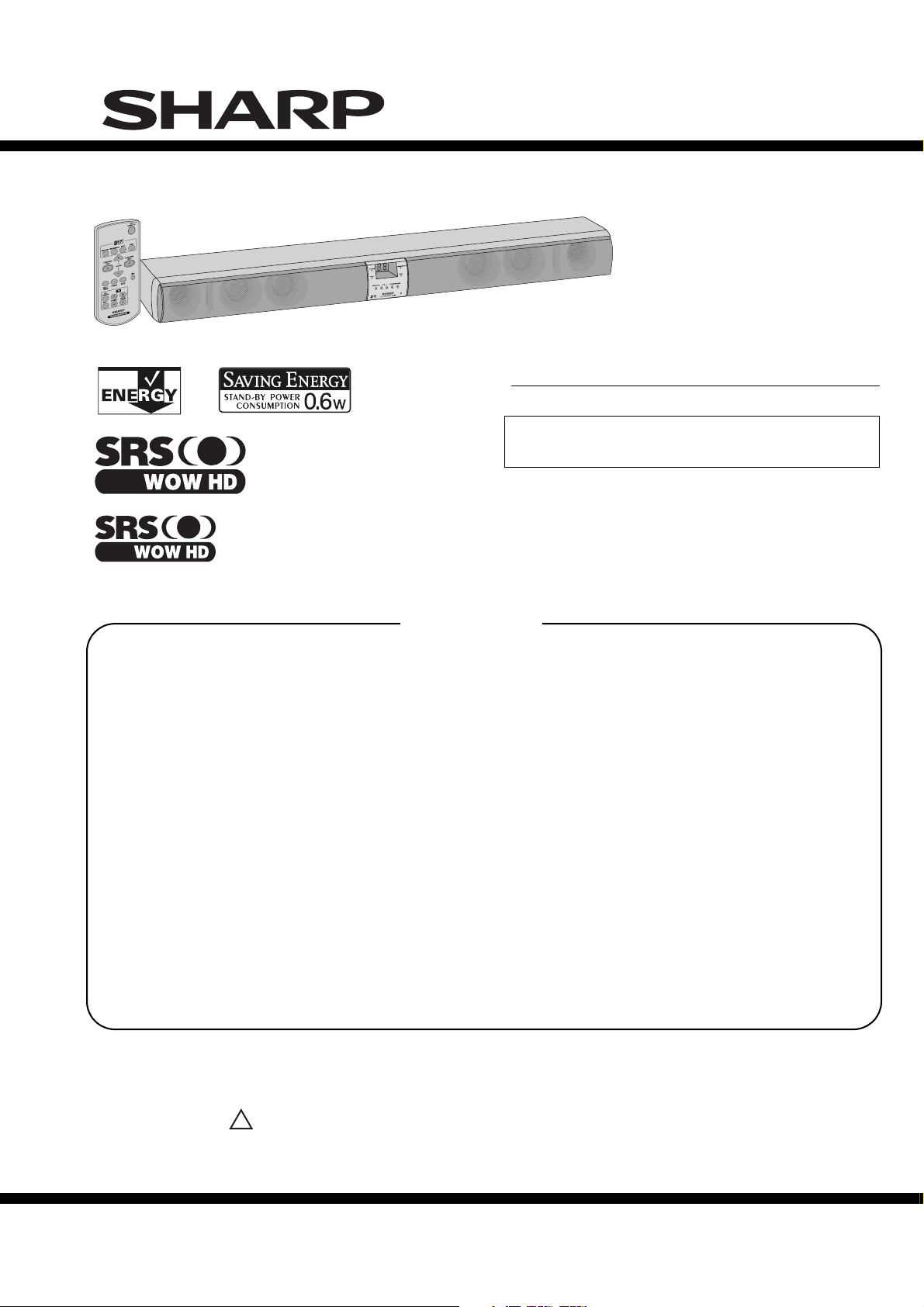
HT-SB200
SERVICE MANUAL
No. S1902HTSB200W
SOUND BAR SYSTEM
is a trademark of SRS Labs, Inc.
WOW HD technology is incorporated under license
from SRS Labs, Inc.
CONTENTS
PRECAUTIONS FOR USING LEAD-FREE SOLDER
CHAPTER 1. GENERAL DESCRIPTION
[1]
AC Power Supply Cord And AC Plug Adaptor
[2] Specifications ................................................ 1-1
[3] Name Of Parts ............................................... 1-2
CHAPTER 2. ADJUSTMENTS
[1] Test Mode....................................................... 2-1
CHAPTER 3. MECHANISM BLOCKS
[1] Disassembly................................................... 3-1
CHAPTER 4. DIAGRAMS
[1] Block Diagrams.............................................. 4-1
.. 1-1
MODEL
• In the interests of user-safety the set should be restored
to its original condition and only parts identical to those
specified be used.
CHAPTER 6. CIRCUIT SCHEMATICS AND PARTS
LAYOUT
[1] Notes On Schematic Diagram .......................6-1
[2] Types Of Transistor And LED........................ 6-1
[3] Schematic Diagram .......................................6-2
[4] Chart Of Connecting Wires............................ 6-8
[5] Wiring Side Of PWB ....................................6-10
CHAPTER 7. OTHERS
[1] Function Table Of IC...................................... 7-1
PARTS GUIDE
HT-SB200
[ ASIA, EX ]
CHAPTER 5. CIRCUIT DESCRIPTION
[1] Voltage ........................................................... 5-1
Parts marked with " " are important for maintaining the safety of the set. Be sure to replace these parts with
specified ones for maintaining the safety and performance of the set.
!
SHARP CORPORATION
This document has been published to be used
for after sales service only.
The contents are subject to change without notice.
Page 2
HT-SB200
PRECAUTIONS FOR USING LEAD-FREE SOLDER
1. Employing lead-free solder
"MAIN, POWER, AMPLIFIER PWB" of this model employs lead-free solder. The LF symbol indicates lead-free
solder, and is attached on the PWB and service manuals. The alphabetical character following LF shows the type
of lead-free solder.
Example:
Indicates lead-free solder of tin, silver and copper.
2.
Using lead-free wire solder
When fixing the PWB soldered with the lead-free solder, apply lead-free wire solder. Repairing with conventional
lead wire solder may cause damage or accident due to cracks.
As the melting point of lead-free solder (Sn-Ag-Cu) is higher than the lead wire solder by 40°C, we recommend
you to use a dedicated soldering bit, if you are not familiar with how to obtain lead-free wire solder or soldering
bit, contact our service station or service branch in your area.
3.
Soldering
As the melting point of lead-free solder (Sn-Ag-Cu) is about 220°C which is higher than the conventional lead
solder by 40°C,and as it has poor solder wet ability, you may be apt to keep the soldering bit in contact with the
PWB for extended period of time. However, since the land may be peeled of for the maximum heat-resistance
temperature of parts may be exceeded, remove the bit from the PWB as soon as you confirm the steady
soldering condition.
Lead-free solder contains more tin, and the end of the soldering bit may be easily corrected. Make sure to turn
on and off the power of the bit as required. If a different type of solder stays on the tip of the soldering bit, it is
alloyed with lead-free solder. Clean the bit after every use of it.
When the tip of the soldering bit is blackened during use, file it with steel wool or fine sand paper.
Be careful when replacing parts with polarity indication on the PWB silk.
Lead-free wire solder for servicing
Ref No.
PWB-A 92LPWB7388MANS MAIN (A1) / POWER (A2) / AMPLIFIER (A3) [ Except Indonesia, Brazil and Taiwan ]
PWB-A 92LPWB7394MANS MAIN (A1) / POWER (A2) / AMPLIFIER (A3) [ For Indonesia Only ]
Parts No.
MAIN (A1) / POWER (A2) / AMPLIFIER (A3) [ For Brazil and Taiwan Only ]PWB-A 92LPWB7387MANS
Description
– i –
Page 3
CHAPTER 1: GENERAL DESCRIPTION
CAUTION : “Danger of explosion if battery is incorrectly replaced. Replace only with the same or
equivalent type”.
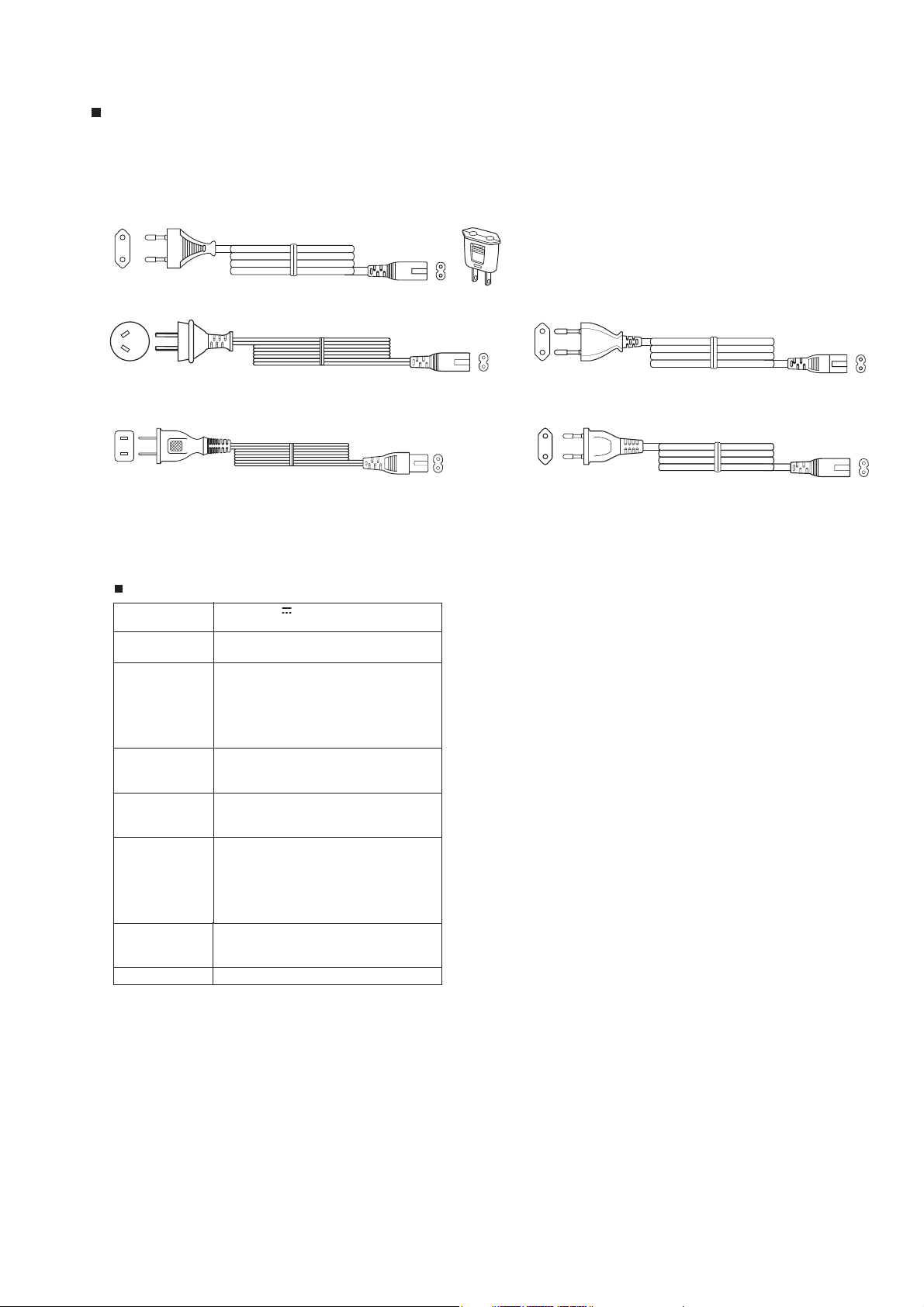
[1] AC Power Supply Cord And AC Plug Adaptor
HT-SB200
QACCEA002AW00
QACCLA002AW00
QACCZA002AW00
[2] Specifications
General
Power source DC IN 12V 4A: AC/DC adaptor
Power
consumption
Output power Front speaker:
Speaker 2.1-way Speaker System
Audio output
terminals
Input terminals Analogue input (LINE 1):
Dimensions Width: 800 mm (31-1/2")
Weight 1.75 kg (3.86 lbs.)
(*) This power consumption value is obtained when in the
power stand-by mode.
(AC 100 - 240 V ~ 50/60 Hz)
Power on: 10 W
Power stand-by: 0.6 W (*)
RMS: 12 W (6 W + 6 W) (10% T.H.D.)
RMS: 9.6 W (4.8 W + 4.8 W) (0.9% T.H.D.)
Subwoofer:
RMS: 20 W (10% T.H.D.)
RMS: 13 W (0.9% T.H.D.)
Front Speakers: 38 mm (1-1/2") Full Range
Subwoofer: 57 mm (2-1/4") Woofer (x4)
Speakers: 12 ohms / Channel
Subwoofer: 3 ohms
(12 Ohms x 4 parallel connections)
RCA type x 1pair (L/R)
500 mV / 47 kohms
Analogue input (LINE 2):
Stereo mini socket Ø 3.5 mm
100 mV / 47 kohms
Height: 96 mm (3-3/4")
Depth: 70 mm (2-3/4")
QPLGA0004AWZZ
QACCZA007AW00
QACCZA018AW00
1 – 1
–2
Page 4
HT-SB200
[3] Names Of Parts
2
TANDARD
S
PORT
S
TAND-BY
S
ON/
S
OUND BAR
VOL.
3
SYSTEM HT-S8200
SURROUND
FUNCTION
CINEMA / GAME
NEWS
451
Front panel
1. Sport Indicator
2. Standard Indicator
3. Information Display
4. Cinema/Game Indicator
5. News Indicator
6 7 8 9
10 11
12
13
1
14
3
1514
6. On/Stand-by Button
7. Volume Down Button
8. Volume Up Button
9. Surround Button
10. Function Button
11. Remote Sensor
12. Left Front Speaker
13. Bass Reflex Duct
14. Subwoofers
15. Right Front Speaker
123
Rear Panel
RIGHT
LEFT
LINE IN 1LINE IN 2
1. Audio Line In 2 (3.5 mm stereo/headphone) Socket
2. Line In 1 (RCA/cinch) Sockets
3. DC Input Socket
Remote Control
1. Remote Control Transmitter
1
8
2
3
4
5
6
7
9
10
11
12
13
14
15
TV Operation Buttons (Only SHARP TV):
On/Stand-by
Button
Volume Up
and Down
Buttons
Notes:
2. Cinema/Game Button
3. Standard Button
4. Volume Up Button
5. Subwoofer Level Down Button
6. Volume Down Button
7. Bass/Treble Button
8. On/Stand-by Button
9. Sport Button
10. News Button
11. Subwoofer Level Up Button
12. Dimmer Button
13. Mute Button
14. Line Button
15. TV Operation Buttons
Sets the TV
power to “ON”
or “STANDBY”.
Turn up/down
the TV
volume.
Some models of SHARP TV may not be operable.
SHARP TV remote will not work with HT-SB200 system.
Input Select
Button (TV)
Channel Up
and Down
Buttons
Press the
button to
switch the
input source.
Switch up/
down the TV
channels.
1 – 2
– 2
Page 5
CHAPTER 2. ADJUSTMENTS
[1] Test Mode
1. Enter the Test Mode version display
While pressing down ON/STANDBY and VOL UP button, Switch ON AC supply.
Version will be display on 7 segment as below:b2 --> ** --> D
b2 = Model name, ( SB200 )
** = Software version no.
D = Destination code :- O (for Others), I (for Indonesia)
2. Enter the Test Mode version display
After enter Test Mode version display, Press VOL UP button.
1. All SOUND MODE LED will light ON
2. 7 segment display will light on if press button as below
Key 7 segment
VOL DOWN 01
VOL UP 02
SURROUND 03
FUNCTION 04
HT-SB200
3. Exit the Test Mode
While in Test Mode function, Press ON/STANDBY button to exit.
4. Error Code Description.
Display Explanation Solution
E1 Communication error between Micom and WM877
E3 Communication error between Micom and STA333
> Unplug AC cord and turn power ON again
> Check line connected between Micom and corresponding ICE2 Communication error between Micom and NJU-26040
5. System Protection indicator
In case abnormal power detection has occurred, the unit will automatically enter to stand-by mode
ON/STANDBY LED willl be flashing as below:-
Flashing
Flashing
OFF OFF
1 Frame
Unit enter Protect mode when irregular process occur on power supply line.
(Repeat)
2 – 1
Page 6
HT-SB200
CD-ES700/CD-ES77CD-ES700/CD-ES77Service ManualCD-ES700/CD-ES77MarketE
CHAPTER 3. MECHANISM BLOCKS
[1] Disassembly
Caution On Disassembly
Follow the below-mentioned notes when disassembling the unit and reassembling it, to keep it safe and ensure
excellent performance:
1. Be sure to remove the power supply plug from the wall outlet before starting to disassemble the unit.
2. Take off nylon bands or wire holders where they need to be removed when disassembling the unit. After servicing
the unit, be sure to rearrange the leads where they were before disassembling.
3. Check that all speaker cushions (refer items 212, 214, 215 and 216 on pages 6 and 7 of Parts Guide) are properly
sealed otherwise vibration noise will be very distinct at low frequency sound.
Replace the cushions if they are found damaged during servicing.
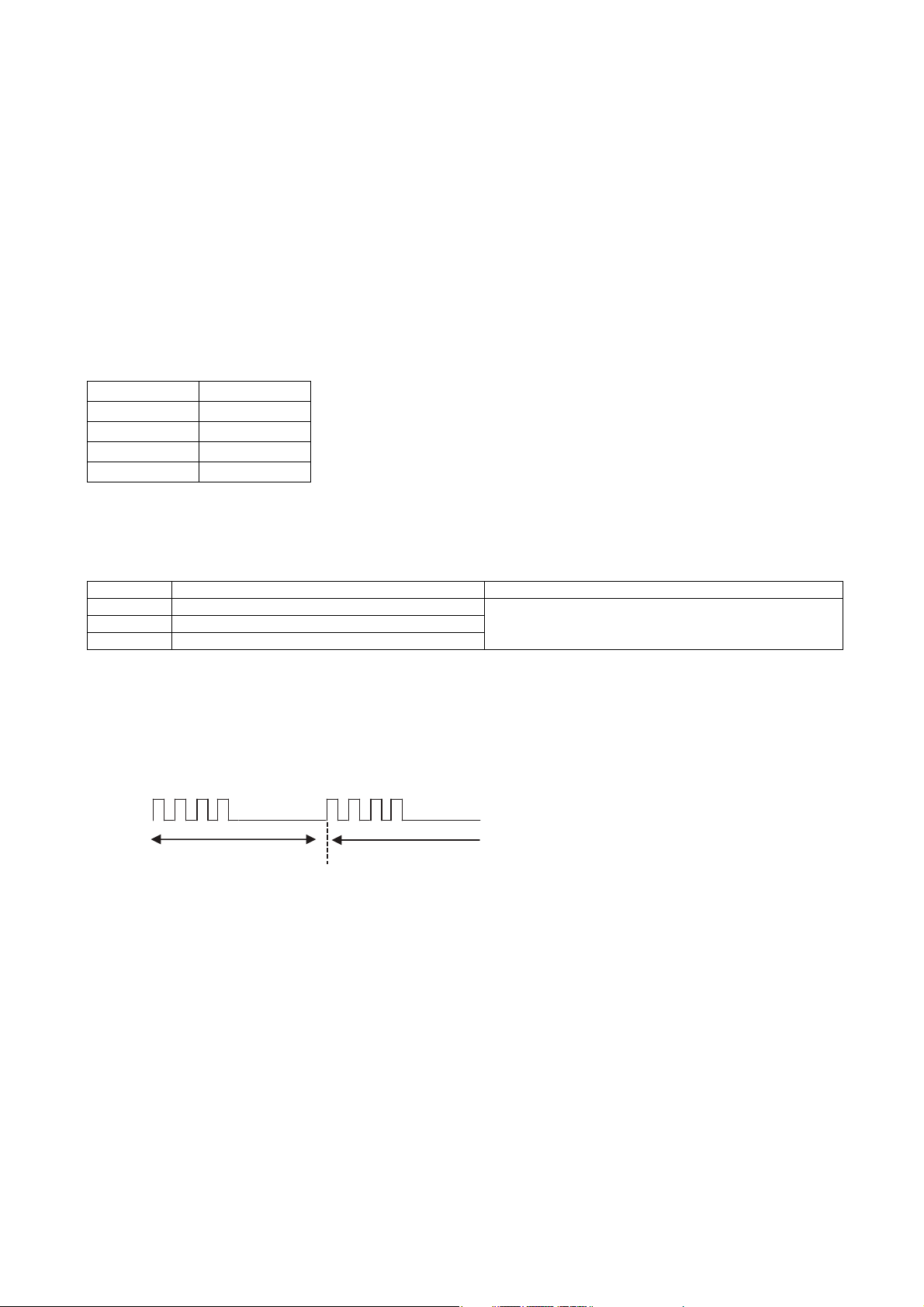
STEP REMOVAL PROCEDURE FIGURE
1 Back Cabinet Assy 1. Wall Mount Bracket…… (A1)x2 1
2. Screw…………..………. (A2)x10
3. Screw…………..………. (A3)x10
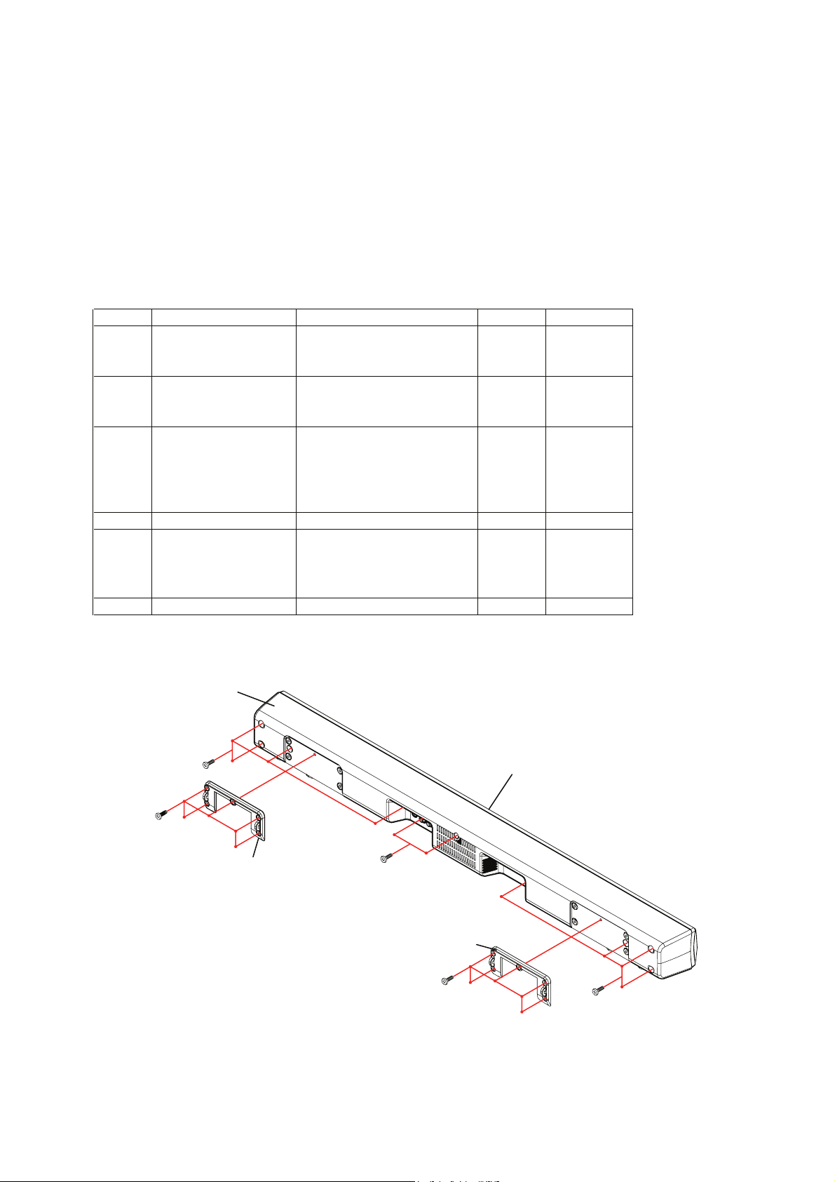
2 Amp PWB 1. Screw……….………….. (B1)x2 2
2. Connector…….……….. (B2)x1
3. Socket………………..… (B3)x2
3 Power PWB 1. Main Chassis……….…. (C1)x1 2
2. Screw………….…….…. (C2)x4
3. Screw………….…….…. (C3)x1
4. Socket………………..…
5. Screw………………...…
4 Main PWB 1. Screw………….………. (D1)x1 2
5 Woofer 1. Duct Port Holder…….… (E1)x2 3
2. Duct Port Assy………… (E2)x2 3
3. Screw………….…….…. (E3)x12 3
2. Screw………….………. (E4)x8 4
6 Speaker 1. Screw………….………. (F1)x8 4
(C4)x1
(C5)x2
Back Cabinet Ass’y
(A3)x4
M3x10mm
(A2)x5
M3.5x10mm
(A1)x1
Wall Mount Bracket
(A3)x2
M3x10mm
(A1)x1
Wall Mount Bracket
(A2)x5
M3.5x10mm
Figure 1
Front Cabinet Ass’y
(A3)x4
M3x10mm
3 – 1
Page 7
Amplifier PWB
(B2)x1
(C1)x1
Main Chassis
(C2)x4
M3x10mm
(B3)x1
(C3)x1
Special Screw
(B1)x2
Special Screw
Figure 2
Main PWB
(B3)x1
(C4)x1
Front Cabinet Ass’y
(D1)x1
M3x8mm
Power PWB
(C5)x2
M3x8mm
HT-SB200
(E3)x6
M3x10mm
Speaker
Woofer
(E2)x1
Duct Port Ass’y
(F1)x4
M2.6x8mm
Woofer
Figure 3
(E4)x2
M3x10mm
Front Cabinet Ass’y
(E1)x1
Duct Port Holder
(E1)x1
Duct Port Holder
(E2)x1
Duct Port Ass’y
(E3)x6
M3x10mm
(E4)x2
M3x10mm
Woofer
Woofer
(E4)x2
M3x10mm
(E4)x2
M3x10mm
Speaker
(F1)x4
M2.6x8mm
LOCKING TAB
SPEAKER
WIRE
SPEAKER UNIT
LOCKING TAB
Figure 4
3 – 2
Front Cabinet Ass’y
CAUTION:
TO REMOVE SPEAKER UNIT, PRESS THESE LOCKING TABS
TO RELEASE SPEAKER WIRES.
Page 8
HT-SB200
A
V
6
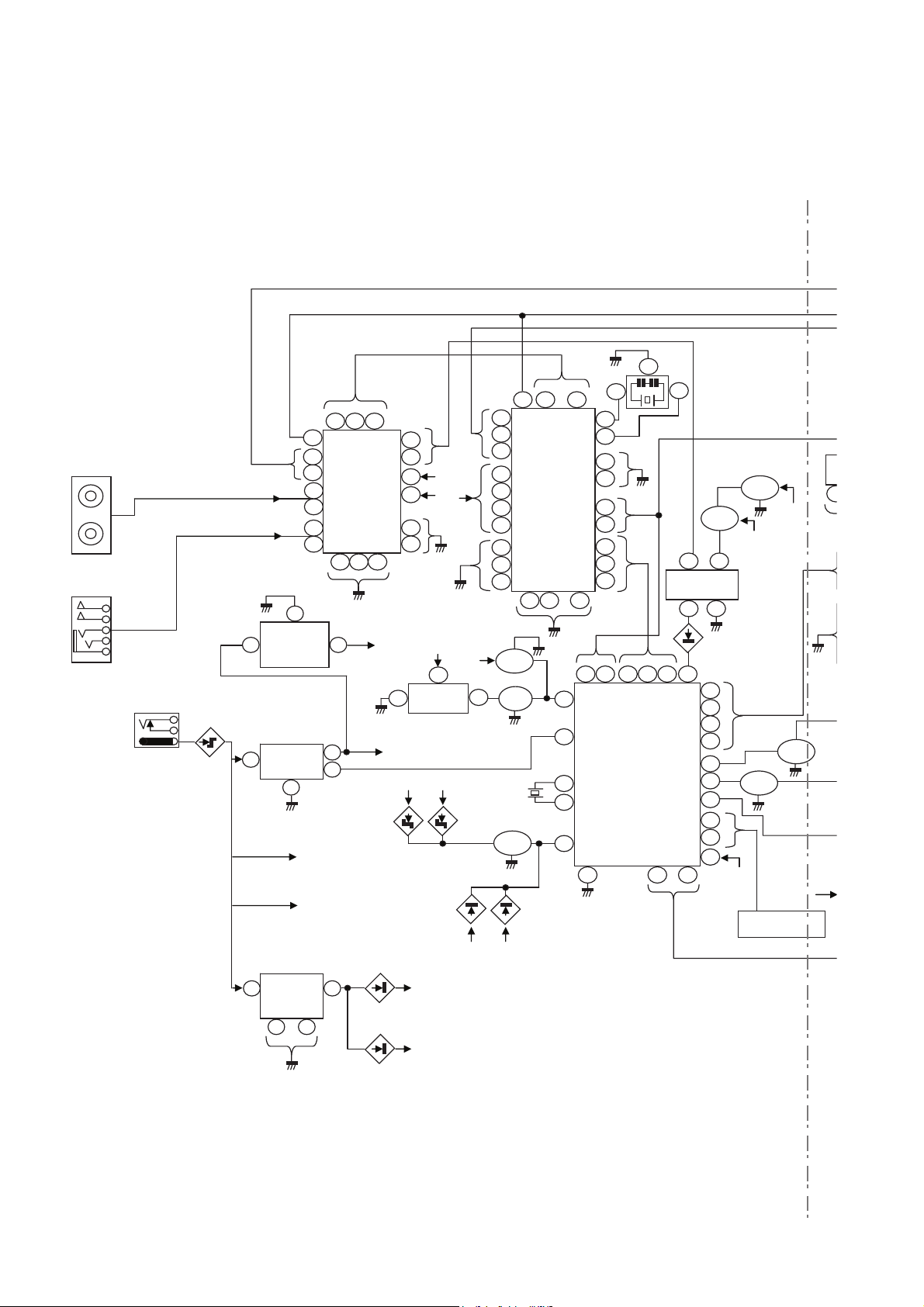
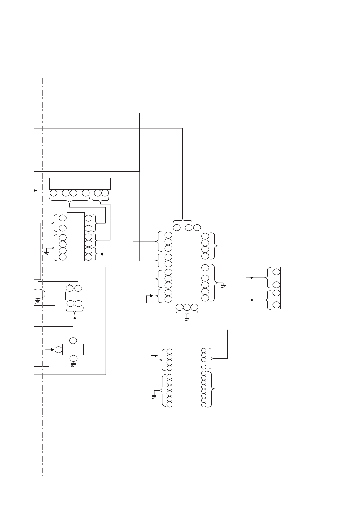
CHAPTER 4. DIAGRAM
[1] Block Diagram
2
1
22
5
2 4
3
JK802 (LINE IN)
hcL
L +B2
R
hcR +B5
10
11
L
R
L
R
1
28
IC601
WM8775
25
24
6 14
JK801 (AUDIO IN)
AVDD
DVDD
17
18
21
+B1
16
7
+B2
8
9
17
18
19
1
7
VDD
8
25
5
9
12
~
3
KIA1117F33L
V02/A5 B25KS
IC801
2
LD29080
1
IC802
3
+B5
+B2
2
V3.3
D
3
4
V0.5AR
1B+
1
+B1 +B4
DZ802 DZ803
5.6B 13A
2
IC605
PST8227N
DC_RLY
Q602
1
Q601
XM603
32.768kHz
Q802
FROM AC/DC
DA
OTPA
L
R 206D3B+
JK803 DZ801
NI C
D
12V 4A
DC_12V
16
14
~
~
IC602
NJU260409
SRS WOW
13 28 32
8
35
7
6
43
10
11
24
23
2
3
6
26
27
42
27 28 30
RESET
POWER
IC604
IXA229AW
SYSTEM
MICROCOMPUTER
SYS
PROTECT
10 4846
MP_12
2
IC803
AP2213
5 8
~
4B+
MICOM_UNSW
3
D604
+B3
UNSW 3.3
+B6
1
08D
+B2 +B1
208D
3
3
IC603
TJM4558CD
1
38
VREF
~
XM601
36.864MHz
Q605
8
4
L6B+
_LV
14
17
18
19
15
20
21
36
42
44
+B3
CETED
Q604
T
Q701
Q702
KEY
SW702-SW705
+B3
1
D605
Figure 4-1: BLOCK DIAGRAM (1/2)
4 – 1
Page 9
+B2
Y
LED701
SEVEN SEGMENT
616 4 5
~ ~
3
HT-SB200
1
701
5
~
2
24
26
27
30
PT6965
4 2
LED702
IC701
1
VDD
3
+B3
9
~
30 27
28
23
31
32
33
34
17
18
19
8
11
~
IC901
STA333BW
POWER IC
SDA
SCL
VCC
22
13
10
9
6
1
~
3
7
12
16
3526
L
R
1
~
L
R
FRONT = 12
4
5
~
SUBWOOFER = 3Ω
8
Ω
15
28
29
8
23
+
1B
+B4
1
2
REMOTE
SENSOR
3
+B4
7
4
12
15
1
5
6
13
14
19
VCC
IC902
STA533W
25
26
32
~
29
2
3
8
9
10
11
16
17
+B3
W705
Figure 4-2: BLOCK DIAGRAM (2/2)
4 – 2
Page 10
HT-SB200
CHAPTER 5.
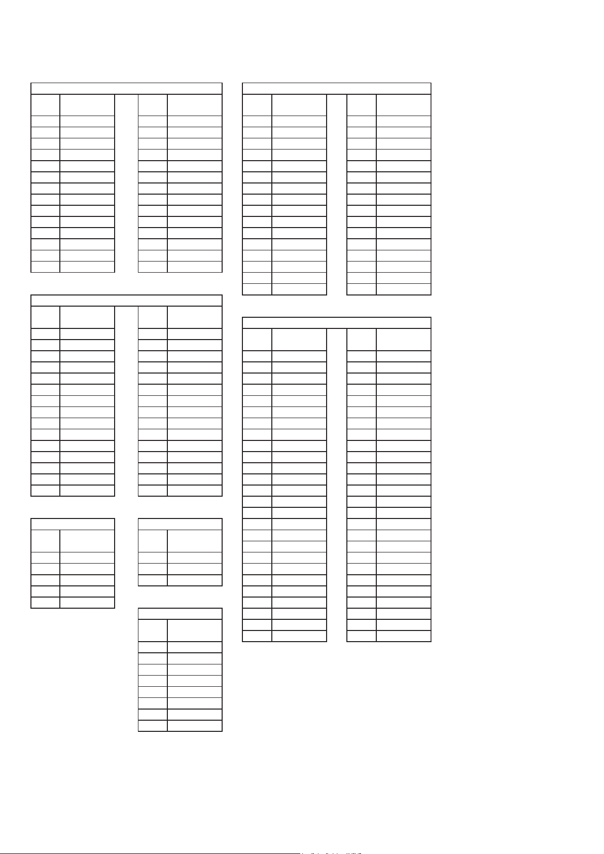
VOLTAGE
[1] Voltage
IC601 IC602
PINNOVOLTAGE
(V)
1 2.45 15 2.45 1 3.28 17 1.63
2 1.64 16 4.91 2 3.27 18 1.64
3 1.62 17 0.00 3 3.13 19 0.90
4 0.81 18 2.45 4
5 1.64 19 2.45 5 0.00 21 0.00
6 0.00 20 2.45 6 3.13 22 1.62
7
8 0.00 22 2.43 8
9 0.00 23 2.43 9 0.00 25 3.28
10 1.52 24 2.44 10 1.55 26 1.65
11 1.50 25 2.44 11 1.54 27 3.12
12 0.00 26 2.43 12 0.00 28 0.00
13 2.43 27 2.43 13 0.00 29 0.00
14 0.00 28 2.45 14 0.80 30 0.00
PINNOVOLTAGE
1 2.45 16 2.45
2 1.64 17 4.91
3 1.62 18 0.00 1
4 0.81 19 2.45 2
5 1.64 20 2.45 3 0.00 29 3.07
6 0.00 21 2.45 4 3.27 30 1.93
7
8 0.00 23 2.43 6 1.43 32 0.00
9 0.00 24 2.43 7 1.07 33 0.00
10 1.52 25 2.44 8 3.10 34 0.00
11 1.50 26 2.44 9 1.43 35 3.13
12 0.00 27 2.43 10 0.00 36 3.06
13 2.43 28 2.43 11 1.56 37 0.00
14 0.00 29 2.45 12 3.13 38 0.00
15 0.00 30 0.00 13 0.00 39 0.00
PINNOVOLTAGE
1 3.05 1 0.00 19 3.28 45 0.00
2 11.75 2 3.28 20 3.10 46 3.13
3 0.00 3 4.94 21 2.96 47 3.13
4 4.94 22 0.00 48 3.27
5 0.00 23 0.00 49 0.00
3.28
IC701
(V)
3.28
IC801 IC802
(V)
PINNOVOLTAGE
(V)
21 2.45 7 3.28 23
PINNOVOLTAGE
(V)
22 2.45 5 3.13 31 0.00
PINNOVOLTAGE
(V)
IC803
PINNOVOLTAGE
(V)
1 11.41
2 11.66
3 3.84
4 2.41
5 0.54
6 0.54
7 0.54
8 0.54
PIN
VOLTAGE
NO
15 1.64 31 0.00
16 1.64 32 0.00
PINNOVOLTAGE
14 2.25 40 0.00
15 0.00 41 0.00
16 0.00 42 3.07
17 1.88 43 3.28
18 1.43 44 3.08
24 0.00 50 0.00
25 0.00 51 0.00
26 0.00 52 0.00
(V)
3.28
3.28
(V)
0.00
3.13
PINNOVOLTAGE
20 0.00
24 0.00
IC604
PINNOVOLTAGE
27 3.12
28 3.12
(V)
0.00
(V)
5 – 1
Page 11
IC901 IC902
PINNOVOLTAGE
(V)
1 0.00 19 3.26 1 0.00 19 0.00
2 0.00 20 3.22 2 0.54 20 0.00
3 0.00 21 3.26 3 0.54 21 4.83
4 8.54 22 0.00 4 11.76 22 4.83
5 11.74 23 3.29 5 0.00 23 3.29
6 0.55 24 3.29 6 0.00 24 4.84
7
8 11.76 26 0.00 8 0.54 26 3.26
9 0.55 27 1.49 9 0.54 27 3.13
10 0.55 28 1.63 10 0.54 28 0.15
11 11.76 29 1.65 11 0.54 29 0.15
12 0.00 30 0.87 12 11.76 30 0.15
13 0.55 31 3.15 13 0.00 31 0.15
14 0.00 32 3.28 14 0.00 32 0.15
15 3.34 33 3.28 15 11.76 33 6.69
16 0.00 34 3.13 16 0.54 34 6.69
17 0.15 35 0.00 17 0.54 35 11.76
18 0.15 36 3.28 18 0.00 36 11.76
0.00
PINNOVOLTAGE
(V)
25 0.00 7
PINNOVOLTAGE
(V)
11.76
PINNOVOLTAGE
(V)
25 3.27
HT-SB200
5 – 2
Page 12

HT-SB200
-MEMO-
5 – 3
Page 13
HT-SB200
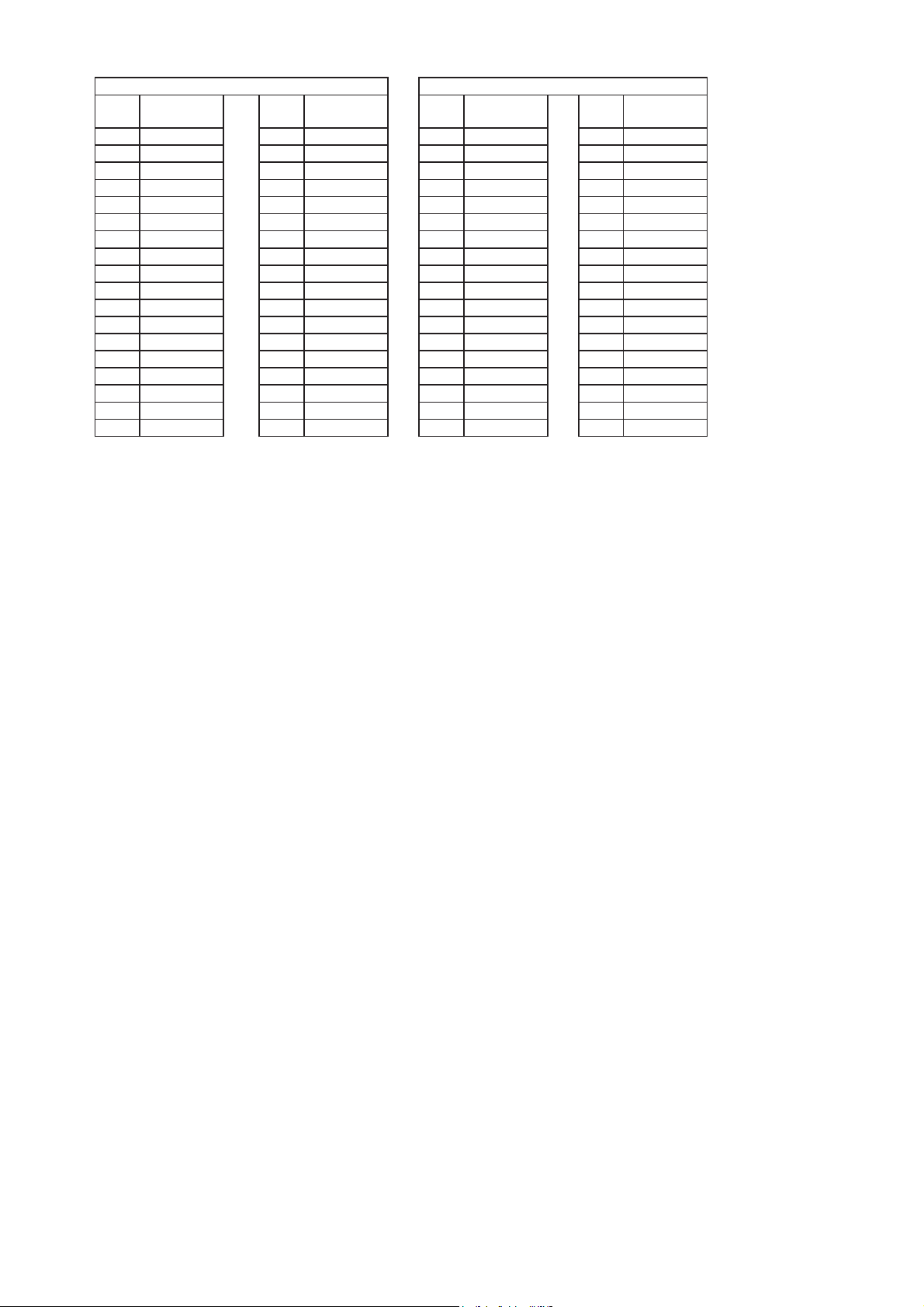
CHAPTER 6. CIRCUIT SCHEMATICS AND PARTS LAYOUT
[1] Notes On Schematic Diagram
•Resistor:
To differentiate the units of resistors, such symbol as
K and M are used: the symbol K means 1000 ohm
and the symbol M means 1000 kohm and the
resistor without any symbol is ohm-type resistor.
Besides, the one with “Fusible” is a fuse type
• Capacitor:
To indicate the unit of capacitor, a symbol P is used:
this symbol P means pico-farad and the unit of the
capacitor without such a symbol is microfarad. As to
electrolytic capacitor, the expression “capacitance/
withstand voltage” is used.
(CH), (TH), (RH), (UJ): Temperature compensation
(ML): Mylar type
(P.P.): Polypropylene type
REF. NO DESCRIPTION POSITION
SW701 POWER ON/STAND-BY ON—OFF
SW702 VOLUME DOWN ON—OFF
SW703 VOLUME UP ON—OFF
SW704 SURROUND ON—OFF
SW705 FUNCTION ON—OFF
• Schematic diagram and Wiring Side of P.W.Board
for this model are subject to change for
improvement without prior notice.
• The indicated voltage in each section is the one
measured by Digital Multimeter between such a
section and the chassis with no signal given.
• Parts marked with “ ” are important for
maintaining the safety of the set. Be sure to replace
these parts with specified ones for maintaining the
safety and performance of the set.
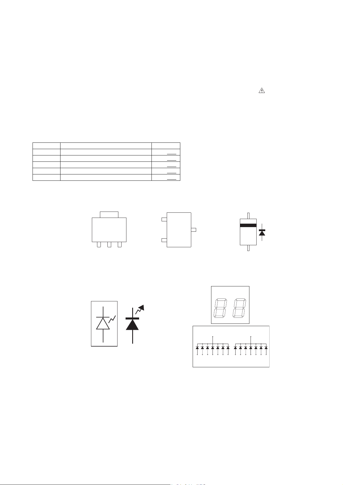
[2] Types Of Transistor And LED
TOP VIEW
B(1) C(2) E(3)
KiA1117F
PCL194H
B
(3)
E
(1)
TOP
VIEW
KRC101S
KRC107S
KRA107S
KRC104S
C
(2)
DIG 1
DIG 2 DIG 2
4
COM
DIG 1
ABCDEFG
15 13 1 3 2 14 16
TOP VIEW
MA111G
KDS226
A
G
FB
CE
D
5
COM
AB
CD E F G
10 12 8 6 7 11 9
DIG 2
6 – 1
PCL165S
Page 14
HT-SB200
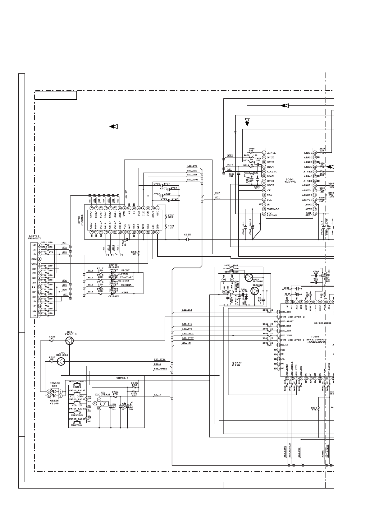
[3] Schematic Diagram
MAIN PWB-A1
A
B
AUDIO SIGNAL
C
D
E
F
G
H
1
23456
Figure 6-1: MAIN SCHEMATIC DIAGRAM (1/2)
6 – 2
Page 15

TABLE 1
Remark
Dest.
Taiwan, Brazil
10KPULL DOWN R638
NIL
Indonesia Others
2.2K
10K
10K
NILPULL DOWN R645
HT-SB200
D_GND
TABLE 1
* Please refer
TAB LE 2
D_GND/PWM_IN
D_GND/PWM_IN
PWM_IN
PWM_IN
TABLE 2
Description of
CNP602 for
PIN no.9
PWM_IN
D_GND
TO AMPLIFIER SECTION
(CNP901)
TO AMPLIFIER SECTION
Taiwan,
Others
Brazil
NIL
NIL
(CNP801)
7
8 9 10 11 12
Figure 6-2: MAIN SCHEMATIC DIAGRAM (2/2)
6 – 3
Page 16
HT-SB200
A
B
TO MAIN SECTION
AUDIO SIGNAL
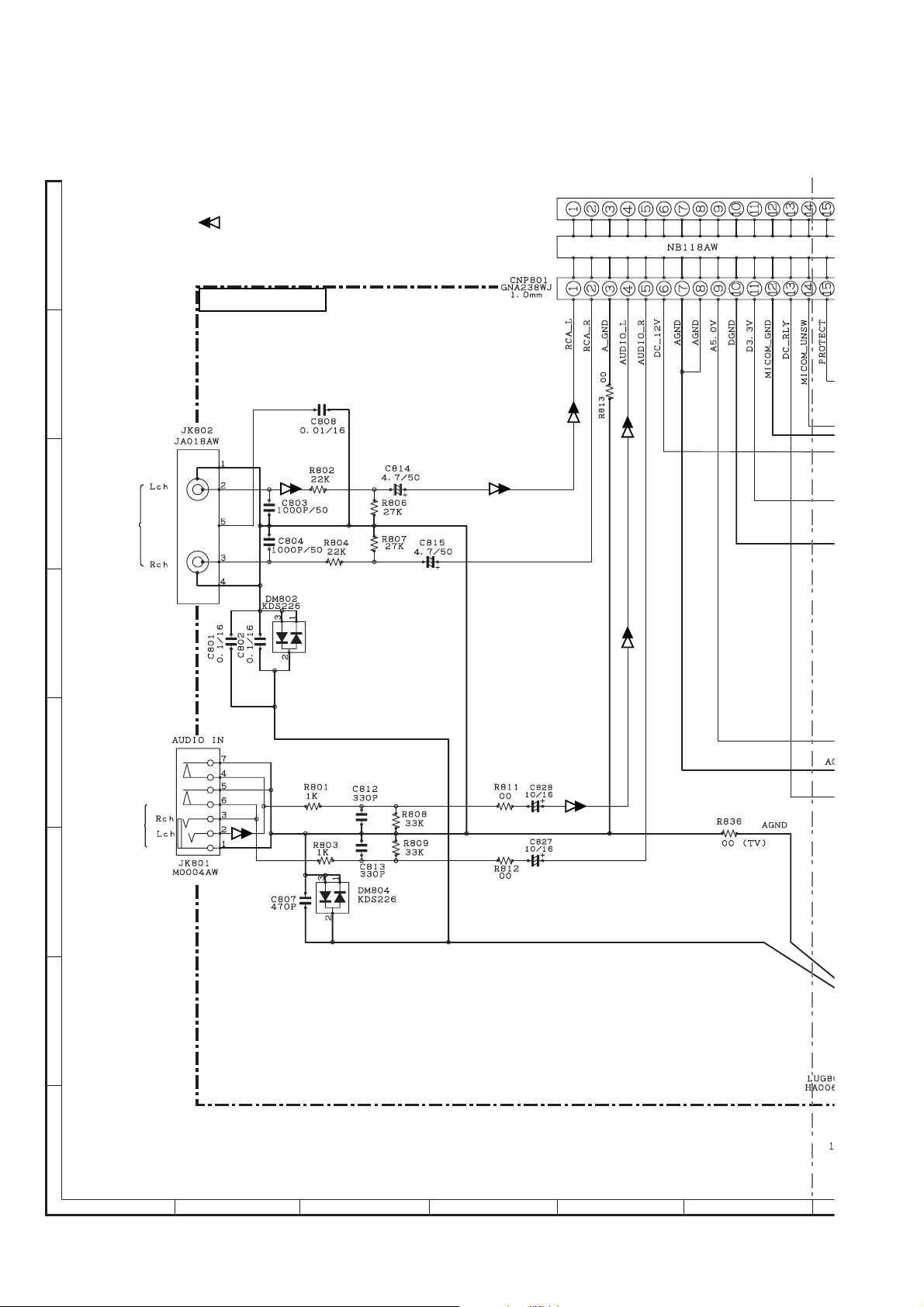
POWER PWB-A2
C
LINE IN 1
D
E
LINE IN 2
F
G
H
1
23456
Figure 6-3: POWER SCHEMATIC DIAGRAM (1/2)
6 – 4
Page 17
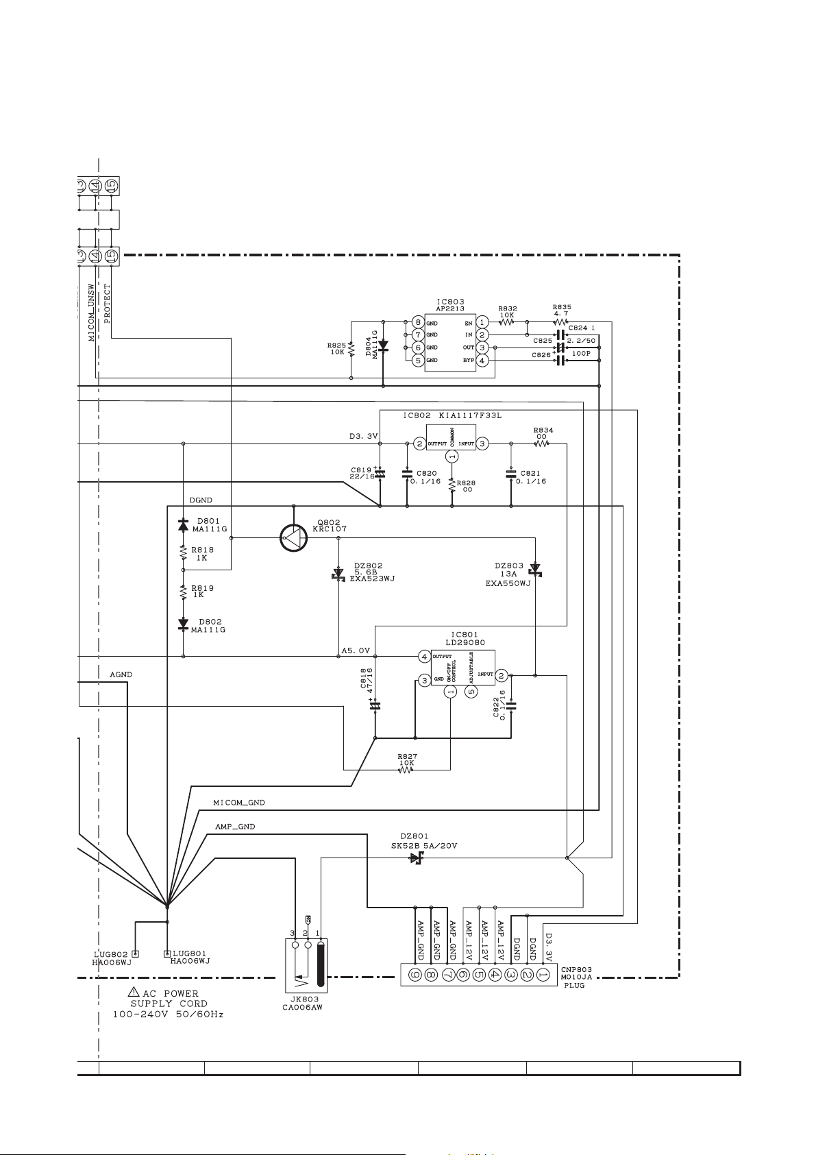
HT-SB200
DC IN
12V, 4A
TO AMPLIFIER SECTION
FROM
AC/DC ADAPTOR
7
8 9 10 11 12
Figure 6-4: POWER SCHEMATIC DIAGRAM (2/2)
6 – 5
Page 18

HT-SB200
i
AUDIO SIGNAL
TABLE 3
Description of CNP901
for PIN no. 9
PWM_IN NIL
D_GND NIL
Taiwan, Brazil
Others
A
B
C
TO MAIN SECTION
D_GND/PWM_IN
*Please refer TABLE 3
D
NOTE
C980 use for others
destination EXCEPT
Taiwan and Brazil
AMP PWB-A3
use for others destination EXCEPT Taiwan and Braz
use for others destination EXCEPT Taiwan and Brazil
E
F
G
H
TO POWER SECTION
1
23456
Figure 6-5: AMPLIFIER SCHEMATIC DIAGRAM (1/2)
6 – 6
Page 19

HT-SB200
w
SPEAKER SYSTEM (R-CH)
SPEAKER
an and Brazil
SP2
WOOFER
SP6
WOOFER
SP5
SPEAKER SYSTEM (L-CH)
WOOFER
SP4
WOOFER
SP3
SPEAKER
SP1
7
8 9 10 11 12
Figure 6-6: AMPLIFIER SCHEMATIC DIAGRAM (2/2)
6 – 7
Page 20

HT-SB200
[4] Charts Of Connecting Wires
A
RF2
CORE
RF1
CNS801-A
9 10111213141587654321
FROM
AMP PWB-A3
CNP901
910111213141587654321
CNP801
JK803
CNP803
DC INPUT
123456789
DC IN 12V , 4A
CNS801-B
BK
BK
BK
BK
BK
BK
B
910111213141587654321
CNP601
1234
CNP603
FOR
C
678912345
206PNC
01
11
9 10111213141587654321
DEVICE ONLY
EXTERNAL MICOM
1
RD
23
BK
BK
4
BK
5
BK
6
7
BK
8
BK
9
BK
01
BK
11
BK
BK
BK
BK
BK
BK
BK
BK
BK
BK
RD
D
CNS602-A
E
JK802
JK801
F
G
H
MAIN PWB-A1
(Top Side)
POWER PWB-A2
(Bottom Side)
AC / DC ADAPTOR
AC POWER SUPPLY CORD
L-CH
R-CH
AUDI O
LINE IN 2
1
2
LINE IN 1
CORE
CYLINDER CORE
(2 x TURN)
AC 100 - 240V ~ 50/60Hz
1
23456
Figure 6-7: WIRING CONNECTION (1/2)
6 – 8
Page 21

HT-SB200
123456789
CNP902
CNP901
CNS903
12345678
CNP903
9876543211011
9876543211011
WH
1
RD
2345678
BK
GY
RD
WH
GY
BK
AMP PWB-A3
(Bottom Side)
CNS602-B
RD
WH
RD
WH
RD
WH
SPEAKER
SP2
WOOFER
SP6
WOOFER
SP5
SPEAKER SYSTEM (R-CH)
RD
BK
BK
BK
BK
BK
TO
MAIN PWB-A1
CNP602
BKBKBK
BK
BK
GY
WOOFER
SP4
BK
GY
WOOFER
BK
GY
BK
SPEAKER SYSTEM (L-CH)
SP3
SPEAKER
SP1
COLOR TABLE
RD
BK
WH
RED
BLACK
WHITE
GY GREY
7
8 9 10 11 12
Figure 6-8: WIRING CONNECTION (2/2)
6 – 9
Page 22

HT-SB200
[5] Wiring Side Of PWB
MAIN PWB-A1
A
B
C
1234
56789
10
11
1234
D
E
10
1112131415
123456789
F
G
Lead-free solder indication
H
Lead-free solder is used in the MAIN PWB.
Refer to "Precautions for handling lead-free solder" for instructions
and precautions.
1
23456
Figure 6-9(i): WIRING SIDE OF MAIN PWB (TOP VIEW) (1/2)
6 – 10
Page 23

HT-SB200
7
8 9 10 11 12
Figure 6-10(i): WIRING SIDE OF MAIN PWB (TOP VIEW) (2/2)
6 – 11
Page 24

HT-SB200
HT-SB200
for Taiwan and Brazil only.
A
MAIN PWB-A1
B
C
6
1
6C
R640
C639
CNP603
1243
C614
9
1
6C
556R
566R
C628
CNP602
C610
R679
34
6C
0
2
6C
086R
C602
386R
C621
C604
LUG601
9
86754321
10 11
146C
246C
C611
44
6
C
1
06L
C636
C637
1
R682
R641
R642
R643
6
73
36R
6
R
33
7
R
R607
R603
IC604
D
R604
R605
R606
E
64
1011121314
15
9
2
8
7
53
CNP601
1
606MD
C633
136C
3
466R
66R
F
G
Lead-free solder indication
H
Lead-free solder is used in the MAIN PWB.
Refer to "Precautions for handling lead-free solder" for instructions
and precautions.
1
23456
Figure 6-9(ii): WIRING SIDE OF MAIN PWB (TOP VIEW) (1/2)
6 – 12
Page 25

HT-SB200
R731
C701
186R
IC701
1
037R
607C
807C
607
70
7C
C
20
7
5
3
6
C
Q
7
2
7
R
107Q
527
R
317R
217R
11
9
01
0
7
7R
7
R
R
2
3
6C
3
466R
66R
5
0
6
D
9
2
6
C
4
0
6
D
2
3
0
0
7
7
C
C
R734
6
53
3
7
7
R
R
166R
R704
807R
707R
5
4
6
1
1
1
7
7R
7
R
R
607R
1
2
307
0
0
7
7
R
R
R
7
8 9 10 11 12
Figure 6-10(ii): WIRING SIDE OF MAIN PWB (TOP VIEW) (2/2)
6 – 13
Page 26

HT-SB200
MAIN PWB-A1
A
B
C
Table of Parts Usage
Remark
Dest.
JP3
JP5
Taiwan, Brazil
USEJP1
NIL
NIL
Indonesia Others
NIL
USE NIL
NIL
NIL
USE
D
NOTE
PLEASE REFER
TABLE OF PARTS
USAGE.
E
F
G
1
JP1
JP3
JP5
Lead-free solder indication
H
Lead-free solder is used in the MAIN PWB.
Refer to "Precautions for handling lead-free solder" for instructions
and precautions.
1
23456
Figure 6-11: WIRING SIDE OF MAIN PWB (BOTTOM VIEW) (1/2)
6 – 14
Page 27

HT-SB200
7
8 9 10 11 12
Figure 6-12: WIRING SIDE OF MAIN PWB (BOTTOM VIEW) (2/2)
6 – 15
Page 28

HT-SB200
POWER PWB-A2
A
B
C
D
DM802
C801
C804
R804
E
DM804
R801
C813
R803
R808
R809
C812
R811
R812
R807
R802
R806
C803
C808
C802
F
G
Lead-free solder indication
H
Lead-free solder is used in the POWER PWB.
Refer to "Precautions for handling lead-free solder" for instructions
and precautions.
1
23456
Figure 6-13: WIRING SIDE OF POWER PWB (TOP VIEW) (1/2)
6 – 16
Page 29

HT-SB200
DZ803
Q802
DZ802
D801
R819 R818
D802
7
8 9 10 11 12
Figure 6-14: WIRING SIDE OF POWER PWB (TOP VIEW) (2/2)
6 – 17
Page 30

HT-SB200
POWER PWB-A2
A
B
C
123456789
D
123456789101112131415
E
F
G
Lead-free solder indication
H
Lead-free solder is used in the POWER PWB.
Refer to "Precautions for handling lead-free solder" for instructions
and precautions.
1
23456
Figure 6-15: WIRING SIDE OF POWER PWB (BOTTOM VIEW) (1/2)
6 – 18
Page 31

HT-SB200
DC INPUT
L-CH
LINE IN 1
R-CH
LINE IN 2
AUDIO
7
8 9 10 11 12
Figure 6-16: WIRING SIDE OF POWER PWB (BOTTOM VIEW) (2/2)
6 – 19
Page 32

HT-SB200
AMP PWB-A3
A
B
C
D
E
F
G
C906
Lead-free solder indication
Lead-free solder is used in the AMPLIFIER PWB.
H
Refer to "Precautions for handling lead-free solder" for instructions
and precautions.
1
23456
Figure 6-17(i): WIRING SIDE OF AMPLIFIER PWB (TOP VIEW)
6 – 20
Page 33

HT-SB200
HT-SB200
for Taiwan and Brazil only.
AMP PWB-A3
A
C967
C963
C966
C964
B
C965
C
C915
R906
C979
C901
C925
C941
R925
C951
C950
C926
C933
R917
L910
C943
C927
R918
C938
C936
C940
C906
L905
C937
R919
C939
C944
C928
L906
C903
D
C924
L908
C942
R923
R922
E
L907
R927
R926
C953
F
G
C948
R929
C958
C952
C959
C955
C949
C954
L913
C957
L912
L909
R928
C956
C947
C946
R924
L914
Lead-free solder indication
Lead-free solder is used in the AMPLIFIER PWB.
H
Refer to "Precautions for handling lead-free solder" for instructions
and precautions.
1
23456
Figure 6-17(ii): WIRING SIDE OF AMPLIFIER PWB (TOP VIEW)
L911
6 – 21
L915
L916
Page 34

HT-SB200
AMP PWB-A3
A
B
C
12345678
D
E
123456789
F
G
12 3456 7891011
Lead-free solder indication
Lead-free solder is used in the AMPLIFIER PWB.
H
Refer to "Precautions for handling lead-free solder" for instructions
and precautions.
1
23456
Figure 6-18: WIRING SIDE OF AMPLIFIER PWB (BOTTOM VIEW)
6 – 22
Page 35

HT-SB200
HT-SB200
for Taiwan and Brazil only.
A
AMP PWB-A3
12345678
B
C
D
987654321
E
F
G
1234567891011
Lead-free solder indication
Lead-free solder is used in the AMPLIFIER PWB.
H
Refer to "Precautions for handling lead-free solder" for instructions
and precautions.
1
23456
Figure 6-19: WIRING SIDE OF AMPLIFIER PWB (BOTTOM VIEW)
6 – 23
Page 36

HT-SB200
A
A
CHAPTER 7. OTHERS
[1] Function Table Of IC
IC601 VHIWM8775++-1 : 96kHz ADC with 4 Channel I/P Multiplexer ( WM8775 ) ( 1/2 )
AINOPL
INOPR
AINVGL
INVGR
AIN1L
AIN1R
AIN2L
AIN2R
AIN3L
AIN3R
AIN4L
AIN4R
INPUT MIXER
AGND
AVDD
VMIDADC
ADCREFP
ADCREFGND
WM8775
AUDIO INTERFACE
VMID
DGND
STEREO
ADC
DVDD
CONTROL INTERFACE
AND
DIGITAL FILTERS
CL
MODE
Figure 7-1 BLOCK DIAGRAM OF IC
CE
MCLK
DOUT
ADCLRC
BCLK
DI
㪘㪠㪥㪈㪣
㪙㪚㪣㪢
㪤㪚㪣㪢
㪛㪦㪬㪫
㪘㪛㪚㪣㪩㪚
㪛㪞㪥㪛
㪛㪭㪛㪛
㪤㪦㪛㪜
㪚㪜
㪛㪠
㪚㪣
㪥㪚
㪭㪤㪠㪛㪘㪛㪚
㪘㪛㪚㪩㪜㪝㪞㪥㪛
㪈
㪉
㪊
㪋
㪌
㪍
㪎
㪏
㪐
㪈㪇
㪈㪈
㪈㪉
㪈㪊
㪈㪋
㪉㪊
㪉㪇
㪈㪐
㪉㪏
㪉㪎
㪉㪍
㪉㪌
㪉㪋
㪉㪉
㪉㪈
㪈㪏
㪈㪎
㪈㪍
㪈㪌
㪘㪠㪥㪈㪩
㪘㪠㪥㪉㪣
㪘㪠㪥㪉㪩
㪘㪠㪥㪊㪣
㪘㪠㪥㪊㪩
㪘㪠㪥㪋㪣
㪘㪠㪥㪋㪩
㪘㪠㪥㪦㪧㪣
㪘㪠㪥㪭㪞㪣
㪘㪠㪥㪦㪧㪩
㪘㪠㪥㪭㪞㪩
㪘㪞㪥㪛
㪘㪭㪛㪛
㪘㪛㪚㪩㪜㪝㪧
Figure 7-2 PIN CONFIGURATION OF IC
7 – 1
Page 37

IC601 VHIWM8775++-1 : 96kHz ADC with 4 Channel I/P Multiplexer ( WM8775 ) ( 2/2 )
PIN NAME TYPE DESCRIPTION
1 AIN1L Analogue Input Channel 1 left input multiplexer virtual ground
2 BCLK Digital Input / Output ADC audio interface bit clock
3 MCLK Digital Input Master ADC clock; 256,384,512 or 768fs (fs = word clock frequency)
4 DOUT Digital Output ADC data output
5 ADCLRC Digital Input / Output ADC left / right word clock
6 DGND Supply Digital negative supply
7 DVDD Supply Digital positive supply
8 MODE Digital Input Serial Interface Mode select
9 CE Digital Input Serial Interface Latch signal
10 DI Digital Input / Output Serial Interface data
11 CL Digital Input Serial Interface clock
12 NC NC No Connection
13 VMIDADC Analogue Output ADC midrail divider decoupling pin; 10uF external decoupling
14 ADCREFGND Supply ADC negative supply and substrate connection
15 ADCREFP Analogue Output ADC positive reference decoupling pin; 10uF external decoupling
16 AVDD Supply Analogue positive supply
17 AGND Supply Analogue negative supply and substrate connection
18 AINVGR Analogue Input Right channel multiplexer virtual ground
19 AINOPR Analogue Output Right channel multiplexer output
20 AINVGL Analogue Input Left channel multiplexer virtual ground
21 AINOPL Analogue Output Left channel multiplexer output
22 AIN4R Analogue Input Channel 4 right input multiplexer virtual ground
23 AIN4L Analogue Input Channel 4 left input multiplexer virtual ground
24 AIN3R Analogue Input Channel 3 right input multiplexer virtual ground
25 AIN3L Analogue Input Channel 3 left input multiplexer virtual ground
26 AIN2R Analogue Input Channel 2 right input multiplexer virtual ground
27 AIN2L Analogue Input Channel 2 left input multiplexer virtual ground
28 AIN1R Analogue Input Channel 1 right input multiplexer virtual ground
IC Pin Descriptions
HT-SB200
7 – 2
Page 38

HT-SB200
IC602 VHINJU260409B : SRS WOW Hardware Data Processor ( NJU26040-09B ) ( 1/2 )
SCL/SCK
SDA/SDOUT
RESETb
MCK
CLK
CLKOUT
AD1/SDIN
SERIAL
HOST
INTERFACE
TIMING
GENERATOR
AD2/SSb
DSP ARITHMETIC UNIT
PROGRAM
CONTROL
24-BIT x 24-BIT
MULTIPLIER
ALU
ADDRESS GENERATION UNIT
DATA
RAM
FIRMWARE
RAM
Figure 7-3 BLOCK DIAGRAM OF IC
SERIAL AUDIO
INTERFACE
L/R
SW
GPIO
BCKO
LRO
SDO0
SD10
SDI1
SDI2
SDO1
BCKI
LRI
PROC
MUTEb
SEL
WDC
VDD
1
RESETb
VDD
VDD
VSS
CLK
SDI2
SDI1
SDI0
LRI
BCKI
2
3
4
5
6
7
8
9
10
11
12
13
14
15
16
SDA/SDOUT
SCL/SCK
AD1/SDIN
AD2/SSb
CLKOUT
NJU26040
SSOP32
32 VSS
31
TEST0
TEST0
30
SEL
29
PROC
28
MUTEb
27
WDC
26
VDD
25
VSS
24
TEST0
23
MCK
22
TEST1
21
20
SDO1
19
SDO0
18
LRO
BCKO
17
Figure 7-4 PIN CONFIGURATION OF IC
7 – 3
Page 39

IC602 VHINJU260409B : SRS WOW Hardware Data Processor ( NJU26040-09B ) ( 2/2 )
PIN NAME Input / Output DESCRIPTION
1,7,8,25 VDD --- Power Supply + 3.3V
2 SDA/SDOUT OD I²C Input / Output / 4-Wire Serial Output. This pin rquires a pull-up resistance in
both I²C bus and 4-Wire serial mode.
3 SCL/SCK I I²C clock / Serial clock
4 AD1/SDIN I I²C Address / Serial In
5 AD2/SSb I I²C Address / Serial Enable
6 RESETb I Reset (RESETb = 'Low' : DSP Reset)
9,24,32 VSS --- GND
10 CLKOUT O OSC Output
11 CLK I OSC Clock Input
12 SDI2 I Audio Data Input 2 (L/R)
13 SDI2 I Audio Data Input 1 (L/R)
14 SDI0 I Audio Data Input 0 (L/R)
15 LRI I LR Clock Input
16 BCKI I Bit Clock Input
17 BCKO O Bit Clock Output
18 LRO O LR Clock Output
19 SDO0 O Audio Data Output 0 (L/R)
20 SDO1 O Audio Data Output 1 (SW)
21 TEST1 O for Test (Non connect)
22 MCK O Master Clock Output for A/D, D/A
23,30,31 TEST0 I - for Test (connected to VSS)
26 WDC OD Watchdog clock output (open drain output)
27 MUTEb I Master Volume level, After Reset DSP ("1" : 0dB "0" : Mute)
28 PROC I After Reset DSP ("1" : Normal "0" : Wait from Command)
29 SEL I Select I²C or Serial bus ( '1' : Serial / '0' : I²C - Bus)
HT-SB200
Note: I : I : Input
I - : Input (Pull-down)
O:Output
OD :Bi-directional (Open Drain) This pin requires a pull-up resistance.
I / O + :Bi-directional (with Pull-up resistance).
I / O - :Bi-directional (with Pull-down resistance).
7 – 4
Page 40

HT-SB200
IC604 RH-IXA229AW00 : System Microcomputer ( IXA229AW ) ( 1/3 )
NAME INPUT/
PIN
NO.
PORT_TYPE
NO USE
1
NC
SCL
2
P3_5/SCL/SSCK
NO USE
3
P3_3/SSI
SDA
4
P3_4/SDA/SCS
MODE
5
MODE
XCIN
6
P4_3/XCIN
XCOUT
7
XCOUT
RESET
8
RESET
XOUT
9
XOUT/P4_7
GND
10
VSS/AVSS
XIN
11
P4_6/XIN
VCC
12
VCC/AVCC
NO USE
13
P2_7/TRDIOD1
LED_CLK
14
P2_6/TRDIOC1
PWR_LED_STBY 2
15
P2_5/TRDIOB1
NO USE
16
P2_4/TRDIOA1
LED_DIN
17
P2_3/TRDIOD0
LED_STB
18
P2_2/TRDIOC0
LED_DOUT
19
P2_1/TRDIOB0
PWR_LED_STBY 1
20
P2_0/TRDIOA0/TRDCLK
RX_IN
21
P1_7/TRAI0/INT1
NO USE
22
P1_6/CLK0
NO USE
23
P1_5/RXD0/(TRAI0)/(INT)
NO USE
24
P1_4/TXD0
NO USE
25
P1_3/KI3/AN11
NO USE
26
NC
SRS_RSTB
27
P4_5/INT0
SRS_MUTE_B
28
P6_6/INT2/TXD1
SYS_STOP
29
P6_7/INT3/RXD1
OUTPUT
---No Use
OUTPUT
OUTPUT
OUTPUT
INPUT INPUT - Connect to VCC with 10 kohm resistor
INPUT
OUTPUT
INPUT INPUT -
OUTPUT - - -
- - - Connect to GND (VSS)
INPUT - - -
---
OUTPUT
OUTPUT
OUTPUT
OUTPUT
OUTPUT
OUTPUT
INPUT
OUTPUT
INPUT
OUTPUT
OUTPUT
OUTPUT
OUTPUT
OUTPUT - - No Use
OUTPUT
OUTPUT
INPUT
FORM
CMOS INPUT/
OUTPUT
CMOS INPUT/
OUTPUT
CMOS INPUT/
OUTPUT
CMOS INPUT/
OUTPUT
CMOS INPUT/
OUTPUT
CMOS INPUT/
OUTPUT
CMOS INPUT/
OUTPUT
CMOS INPUT/
OUTPUT
CMOS INPUT/
OUTPUT
CMOS INPUT/
OUTPUT
CMOS INPUT/
OUTPUT
CMOS INPUT/
OUTPUT
CMOS INPUT/
OUTPUT
CMOS INPUT/
OUTPUT
CMOS INPUT/
OUTPUT
CMOS INPUT/
OUTPUT
CMOS INPUT/
OUTPUT
CMOS INPUT/
OUTPUT
CMOS INPUT/
OUTPUT
CMOS INPUT/
OUTPUT
CMOS INPUT/
OUTPUT
SOFT
PULL-UP
OFF [12C bus] Enhancer Micom IF clock, N-ch open drain.
OFF No Connect
OFF
OFF No Use
OFF No Use
OFF Fix “L”
OFF LED DRIVER CONTROL CLOCK
OFF
OFF Fix “L”
OFF
OFF LED DRIVER STROBE CONTROL
OFF
OFF
OFF [INT] SHARP format, REMOCON input
OFF Fix “L”
OFF Fix “L”
OFF Fix “L”
OFF Fix “L”
OFF SRS_Reset
OFF SRS_Mute
OFF
[12C bus] Enhancer Micom IF data Input/Output,
N-ch open drain.
Micom reset input. Active is L.
During FLASH, connect to reset at WRITER.
Micom input supply (3.3V)
Backup power supply
H setting: LED ON
L setting: LED OFF
Communication with LED DRIVER.
Command transmit (Data transfer to FLASH WRITER)
Communication with LED DRIVER.
Command received (Data transfer to FLASH WRITER)
H setting: LED ON
L setting: LED OFF
AC power fail detect.
Enter STOP mode when detect SYS_STOP “L”
FUNCTION OUTLINE
7 – 5
Page 41

IC604 RH-IXA229AW00 : System Microcomputer ( IXA229AW ) ( 2/3 )
NAME INPUT/
PIN
NO.
PORT_TYPE
SRS_WDC
30
P1_2/KI2/AN10
NO USE
31
P1_1/KI1/AN9
NO USE
32
P1_0/KI0/AN8
NO USE
33
P3_1/TRB0
NO USE
34
P3_0/TRA0
POWER (DC RELAY)
35
P6_5/CLK1
KEY POWER
36
P6_4
NO USE
37
P6_3
LVL_DETECT
38
P0_7/AN0
NO USE
39
NC
NO USE
40
NC
AREA
41
P0_6/AN1
KEY_1
42
P0_5/AN2
SYS_PROTECT
43
P0_4/AN3
VREF
44
P4_2/VREF
NO USE
45
P6_0/TRE0
AMP_PWDN
46
P6_2
AMP_RESET
47
P6_1
AMP_INT
48
P0_3/AN4
NO USE
49
P0_2/AN5
NO USE
50
P0_1/AN6
NO USE
51
P0_0/AN7
NO USE
52
P3_7/SS0
OUTPUT
INPUT
OUTPUT
OUTPUT
OUTPUT
OUTPUT
OUTPUT
INPUT
OUTPUT
INPUT ANALOG/
DIGITAL
- - - Port not connected
- - - Port not connected
INPUT ANALOG/
DIGITAL
INPUT ANALOG/
DIGITAL
INPUT ANALOG/
DIGITAL
INPUT INPUT - Reference Voltage input port (connect to VCC)
OUTPUT
OUTPUT
OUTPUT
INPUT
OUTPUT
OUTPUT
OUTPUT
OUTPUT
FORM
CMOS INPUT/
OUTPUT
CMOS INPUT/
OUTPUT
CMOS INPUT/
OUTPUT
CMOS INPUT/
OUTPUT
CMOS INPUT/
OUTPUT
CMOS INPUT/
OUTPUT
CMOS INPUT/
OUTPUT
CMOS INPUT/
OUTPUT
CMOS INPUT/
OUTPUT
CMOS INPUT/
OUTPUT
CMOS INPUT/
OUTPUT
CMOS INPUT/
OUTPUT
CMOS INPUT/
OUTPUT
CMOS INPUT/
OUTPUT
CMOS INPUT/
OUTPUT
CMOS INPUT/
OUTPUT
CMOS INPUT/
OUTPUT
CMOS INPUT/
OUTPUT
CMOS INPUT/
OUTPUT
CMOS INPUT/
OUTPUT
SOFT
PULL-UP
OFF SRS_WDC
OFF Fix “L”
OFF Fix “L”
OFF Fix “L”
OFF Fix “L”
OFF
OFF MAIN SET KEY (POWER)
OFF Fix “L”
OFF LEVEL DETECT
OFF Destination setting
OFF [A/D] Main set key input
OFF System power abnormal detection
OFF Fix “L”
OFF
OFF
OFF AMP Interrupt
OFF Fix “L”
OFF Fix “L”
OFF Fix “L”
OFF Fix “L”
MAIN POWER CONTROL.
H: POWER ON ; L: POWER OFF
AMP PWR DOWN = set L during standby
Normal operation = set H
AMP Reset Set 'L' to reset AMP
Normal operation set 'H'
HT-SB200
FUNCTION OUTLINE
7 – 6
Page 42

HT-SB200
IC604 RH-IXA229AW00 : System Microcomputer ( IXA229AW ) ( 3/3 )
NO USE
NO USE
NO USE
51
52
P3_7/SS0
NO USE 1 NC NC 39 NO USE
P3_5/SCL/SSC
SCL
NO USE 3 P3_3/SSI P6_3 37 NO USE
SDA 4
MODE
XCIN 6 P4_3/XCIN P3_0/TRA0 34 NO USE
XCOUT
RESET
XOUT
GND
XIN
VCC 12 VCC/AVCC P6_6/INT2/TXD1 28 SRS_MUTE_B
NO USE
2
K
P3_4/SDA/SC
S
5 MODE P6_5/CLK1 35 POWER (DC RELAY)
7 XCOUT P3_1/TRB0 33 NO USE
8
RESET
9
XOUT/P4_7
10
VSS/AVSS
11
P4_6/XIN
P2_7/TRDIOD
13
1
50
P0_0/AN7
P0_1/AN6
AMP_INT
AMP_RESET
NO USE
48
49
P0_2/AN5
P0_3/AN4
AMP_PWDN
NO USE
47
P6_1
IXA229A
45
46
P6_2
P6_0/TRE0
SHARP
VREF
44
P4_2/VREF
SYS_PROTECT
KEY_1
43
42
P0_4/AN3
P0_5/AN2
AREA
41
P0_6/AN1
NO USE
40
NC
P0_7/AN0
P1_0/KI0/AN8
P1_1/KI1/AN9
P1_2/KI2/AN10
P6_7/INT3/RXD
P4_5/INT0
38 LVL_DETECT
P6_4 36 KEY POWER
32
31
30
29
27 SRS_RSTB
NO USE
NO USE
SRS_WDC
SYS_STOP
P2_6/TRDIOC1
P2_5/TRDIOB1
14
15
LED_CLK
'PWR_LED_STBY 2
P1_6/CLK0
P2_4/TRDIOA1
P2_3/TRDIOD0
P2_2/TRDIOC0
17
LED_DIN
18
LED_STB
16
NO USE
P2_1/TRDIOB0
19
LED_DOUT
P2_0/TRDIOA0/TRD
CLK
20
PWR_LED_STBY 1
P1_7/TRAI0/INT1
21
RX_IN
P1_5/RXD0/(TRAI0)/
(INT)
23
22
NO USE
NO USE
Figure 7-5 BLOCK DIAGRAM OF IC
P1_3/KI3/AN11
P1_4/TXD0
24
NO USE
NC
25
26
NO USE
NO USE
7 – 7
Page 43

IC901 VHISTA333BW-1 : 2.1 Channels High Efficiency Digital Audio System ( STA333BW ) ( 1/2 )
HT-SB200
SA
SDI
LRCKI
BICKI
RESET
INT LINE
PWDN
XTI
Serial Data Input
Channel mapping
Processor
SCL
SDA
I2C
CONTROL
STATUS
EQ, Tone,
Volumes...
PLL
PLL_FILTER
Figure 7-6 BLOCK DIAGRAM OF IC
CONFIG
POWER
DDX3A
DDX3B
DDX4A/TWARNEXT
DDX4B/EAPD
OUT1A
OUT1B
OUT2A
OUT2B
GND_SUB
SA
TEST MODE
VSS
VCC_REG
OUT2B
GND2
V
cc2
OUT2A
OUT1B
V
cc1
GND1
OUT1A
GND_REG
Vdd
CONFIG
OUT3B/DDX3B
OUT3A/DDX3A
1
2
3
4
5
6
7
8
9
10
11
12
13
14
15
16
17
18
Figure 7-7 PIN CONFIGURATION OF IC
V
36
35
34
33
32
31
30
29
28
27
26
25
24
23
22
21
20
19
dd_DIG
GND_DIG
SCL
SDA
INT_LINE
RESET
SDI
LRCKI
BICKI
XTI
PLL_GND
PLL_FILTER
PLL_Vdd
POWRDN
GND_DIG
VDD_DIG
TWARN/OUT4B
EAPD/OUT4B
7 – 8
Page 44

HT-SB200
IC901 VHISTA333BW-1 : 2.1 Channels High Efficiency Digital Audio System ( STA333BW ) ( 2/2 )
PIN NAME TYPE DESCRIPTION
1 GND_SUB Input / Output Subtrate ground
2 SA Input I²C Select Address
3 Test_Mode Input This pin must be connected to GROUND
4 Vss Input / Output Internal reference at Vcc - 3.3V
5 Vcc_REG Input / Output Internal Vcc reference
6 OUT2B Output Output half bridge 2B
7 GND2 Input / Output Power negative supply
8 Vcc2 Input / Output Power positive supply
9 OUT2A Output Output half bridge 2A
10 OUT1B Output Output half bridge 1B
11 Vcc1 Input / Output Power positive supply
12 GND1 Input / Output Power negative supply
13 OUT1A Input / Output Output half bridge 1A
14 GND_REG Input / Output Internal Ground reference
15 Vdd Input / Output Internal 3.3V reference voltage
16 CONFIG Input Paralleled mode command
17 OUT3B/DDX3B Output PWM Out CH3B - External Bridge
18 OUT3A/DDX3A Output PWM Out CH3A - External Bridge
19 EAPD/OUT4A Output Power Down for External Bridge
20 TWARN/OUT4B Input Thermal warning from External Bridge
21 Vdd_DIG Input / Output Positive Supply Digital
22 GND_DIG Input / Output Digital Ground
23 PWRDN Input Power Down
24 PLL_Vdd Input / Output Positive Supply for PLL
25 PLL_FILTER Input Connection to PLL Filter
26 PLL_GND Input / Output Negative Supply for PLL
27 XTI Input PLL Input Clock
28 BICKI Input I²S Serial Clock
29 LRCKI Input I²S Left / Right Clock
30 SDI_12 Input I²S Serial Data Channels 1&2
31 RESET Input Reset
32 INT_LINE Output Fault Interrupt
33 SDA Input / Output I²C Serial Data
34 SCL Input I²C Serial Clock
35 GND_DIG Input / Output Digital Ground
36 Vdd_DIG Input / Output Digital Supply
7 – 9
Page 45

IC902 VHISTA533W+-1 : 2.2A QUAD POWER HALF BRIDGE ( STA533W ) ( 1/2 )
HT-SB200
GND-SUB
OUT2B
OUT2B
Vcc2B
GND2B
GND2A
Vcc2A
OUT2A
OUT2A
OUT1B
OUT1B
Vcc1B
GND1B
GND1A
Vcc1A
OUT1A
OUT1A
1
2
3
4
5
6
7
8
9
10
11
12
13
14
15
16
17
36
35
34
33
32
31
30
29
28
27
26
25
24
23
22
21
20
VccSign
VccSign
V
ss
V
ss
IN2B
IN2A
IN1B
IN1A
TH_WAR
FAULT
TRI-STATE
PWRDN
CONFIG
L
V
V
DD
V
DD
GND-Reg
N.C.
18
19
D04AU1564
Figure 7-8 BLOCK DIAGRAM OF IC
GND-Clean
7 – 10
Page 46

HT-SB200
IC902 VHISTA533W+-1 : 2.2A QUAD POWER HALF BRIDGE ( STA533W ) ( 2/2 )
PIN NAME DESCRIPTION
1 GND_SUB Subtrate ground
2 ; 3 OUT2B Output half bridge 2B
4 Vcc2B Positive Supply
5 GND2B Negative supply
6 GND2A Negative supply
7 Vcc2A Positive Supply
8 ; 9 OUT2A Output half bridge 2A
10 ; 11 OUT1A Output half bridge 1B
12 Vcc1B Positive Supply
13 GND1B Negative supply
14 GND1A Negative supply
15 Vcc1A Positive Supply
16 ; 17 OUT1A Output half bridge 1A
18 NC Not Connected
19 GND-clean Logical Ground
20 GND-Reg Ground for regulator Vdd
21 ; 22 Vdd 5V Regulator referred to ground
23 VL Logic Reference Voltage
24 CONFIG Configuration pin
25 PWRDN Stand-by pin
26 TRI-STATE Hi-Z pin
27 FAULT Fault pin advisor
28 TH-WAR Thermal warning advisor
29 IN1A Input half bridge 1A
30 IN1B Input half bridge 1B
31 IN2A Input half bridge 2A
32 IN2B Input half bridge 2B
33 ; 34 Vss 5V Regulator referred to +Vcc
35 ; 36 Vcc Sign Signal Positive Supply
7 – 11
Page 47

Destination Table
AU Australia
BR Brazil
ID Indonesia
JO Jordan
ME Middle East/Africa/Vietnam
PH Philippines
SI Singapore
TA Taiwan
TH Thailand
PARTS GUIDE
SOUND BAR SYSTEM
MODEL
HT-SB200
HT-SB200
[ ASIA, EX ]
CONTENTS
[1] INTEGRATED CIRCUITS
[2] TRANSISTORS
[3] DIODES
[4] COILS
[5] CRYSTALS / VIBRATORS
[6] CAPACITORS
[7] RESISTORS
[8] OTHER CIRCUITRY PARTS
[9] CABINET PARTS
[10] ACCESSORIES / PACKING
PARTS
[11] P.W.B. ASSEMBLY
(Not Replacement Item)
Parts marked with " " are important for maintaining the safety of the set. Be sure to replace these parts with
specified ones for maintaining the safety and performance of the set.
!
SHARP CORPORATION
This document has been published to be used for
after sales service only.
The contents are subject to change without notice.
Page 48

HT-SB200
NO. PARTS CODE
PRICE
RANK
NEW
MARK
PAR T
RANK
DESCRIPTION
[1] INTEGRATED CIRCUITS
iC601 VHiWM8775++-1 AR ADC with 4 Channel I/P Multiplexer
iC602 VHiNJU260409B AX SRS WOW Hardware Data Processor
iC603 VHiTJM4558CD1 AE Operational Amplifier
iC604 RH-iXA229AW00 AX System Microcomputer,iXA229AW
iC605 VHiPST8227N-1 AC Reset iC
iC701 VHiPT6965++-1 AK 7 Segment Driver
iC801 VHiLD29080+-1 AG Voltage Regulator, 5V
iC802 VHiKiA1117F33 AF Voltage Regulator
iC803 VHiAP2213M33E AE Voltage Regulator, 3.3V
iC901 VHiSTA333BW-1 AW Digital Amplifier
iC902 VHiSTA533W+-1 AP 2.2A Quad Power Half Bridge
[2] TRANSISTORS
Q601 VSKRC104S//-1 AC Digital,NPN,KRC104 S
Q602 VSKRC104S//-1 AC Digital,NPN,KRC104 S
Q604 VSKRC104S//-1 AC Digital,NPN,KRC104 S
Q605 VSKRA107S//-1 AB Digital,PNP,KRA107 S
Q701 VSKRC101S//-1 AB Digital,NPN,KRC101 S
Q702 VSKRC101S//-1 AB Digital,NPN,KRC101 S
Q802 VSKRC107S//-1 AB Digital,NPN,KRC107 S
Q901 VSKRC104S//-1 AC Digital,NPN,KRC104 S [Except Taiwan and Brazil]
Q902 VSKRC104S//-1 AC Digital,NPN,KRC104 S [Except Taiwan and Brazil]
[3] DIODES
D601 VHDMA111G++-1 AB Silicon,MA111
D602 VHDMA111G++-1 AB Silicon,MA111
D603 VHDMA111G++-1 AB Silicon,MA111
D604 VHDMA111G++-1 AB Silicon,MA111
D605 VHDMA111G++-1 AB Silicon,MA111
D801 VHDMA111G++-1 AB Silicon,MA111
D802 VHDMA111G++-1 AB Silicon,MA111
D804 VHDMA111G++-1 AB Silicon,MA111
D901 VHDMA111G++-1 AB Silicon,MA111
D902 VHDMA111G++-1 AB Silicon,MA111 [Except Taiwan and Brazil]
D903 VHDMA111G++-1 AB Silicon,MA111 [Except Taiwan and Brazil]
D904 VHDMA111G++-1 AB Silicon,MA111 [Except Taiwan and Brazil]
D905 VHDMA111G++-1 AB Silicon,MA111 [Except Taiwan and Brazil]
DM606 VHDKDS226//-1 AB Silicon,KDS226
DM802 VHDKDS226//-1 AB Silicon,KDS226
DM804 VHDKDS226//-1 AB Silicon,KDS226
DZ600 RH-EXA507WJZZ AB Zener,3.3V
DZ801 VHDGDSK52B+-1 AE Schotty
DZ802 RH-EXA523WJZZ AB Zener,5.6V
DZ803 RH-EXA550WJZZ AB Zener,13V
LED701 VHPKW2402CB-1 AT 7 Segment Blue LED
LED702 VHPCL165SRD-1 AD Dual Chip LED,Red
LED703 VHPCL194HB+-1 AD LED,Blue
LED704 VHPCL194HB+-1 AD LED,Blue
LED705 VHPCL194HB+-1 AD LED,Blue
LED706 VHPCL194HB+-1 AD LED,Blue
[4] COILS
L601 VPBNN2R2K0000 AC Coil, 2.2 µH
L901 RBLN-0061TAZZ AB Ferrite Bead
L902 RBLN-0061TAZZ AB Ferrite Bead
L903 RBLN-0061TAZZ AB Ferrite Bead
L905 RCiLPA084WJZZ AD Coil, 10 µH
L906 RCiLPA084WJZZ AD Coil, 10 µH
L907 RCiLPA762WJQZ AD Coil
L908 RCiLPA762WJQZ AD Coil
L909 RCiLPA762WJQZ AD Coil
L910 RCiLPA762WJQZ AD Coil
L911 RCiLCA022AWZZ AC Coil, 1 µH
L912 RCiLCA022AWZZ AC Coil, 1 µH
L913 RCiLCA022AWZZ AC Coil, 1 µH
L914 RCiLCA022AWZZ AC Coil, 1 µH
L915 RBLN-A007WJZZ AC Ferrite Core
L916 RBLN-A007WJZZ AC Ferrite Core
R678 RFiLN0063CFZZ AA Ferrite Bead
R907 VPCEM470M3R7N AC Coil, 47 µH
R916 VPCEM470M3R7N AC Coil, 47 µH
RF1 RCORFA016AWZZ AE Ferrite Core
RF2 RCORFA016AWZZ AE Ferrite Core
[5] CRYSTALS / VIBRATORS
XM601 RCRM-A010AWZZ AD Resonator
XM603 RCRSC0032TAZZ AE Crystal,32.768kHz
[6] CAPACITORS
C601 VCCCCZ1HH330J AB 33 pF (CH),50V
C602 VCEAPS106AF1C AB 10 µ F,16V,Electrolytic
C603 VCKYCZ1CF104Z AB 0.1 µ F,16V
C604 VCEAPS106AF1C AB 10 µ F,16V,Electrolytic
C605 VCKYCZ1CF104Z AB 0.1 µ F,16V
C607 VCCCCZ1HH150J AA 15 pF (CH),50V
C608 VCCCCZ1HH180J AA 18 pF (CH),50V
1
Page 49

HT-SB200
NO. PARTS CODE
PRICE
RANK
NEW
MARK
PAR T
RANK
[6] CAPACITORS
C609 VCKYCZ1CF104Z AB 0.1 µ F,16V
C610 VCEAPS106AF1C AB 10 µ F,16V,Electrolytic
C611 VCEAPS106AF1C AB 10 µ F,16V,Electrolytic
C612 VCKYCZ1CF104Z AB 0.1 µ F,16V
C613 VCKYCZ1CB103K AB 0.01 µ F,16V
C614 VCEAPS475AF1H AD 4.7 µ F,50V,Electrolytic
C615 VCKYCZ1CB103K AB 0.01 µ F,16V
C616 VCEAPS106AF1C AB 10 µ F,16V,Electrolytic
C617 VCKYCZ1CB223K AB 0.022 µ F,16V
C618 RC-KZ3007AWZZ AC 2.2 µ F,16V,Electrolytic
C619 VCKYCZ1AB104K AB 0.1 µ F,10V
C620 VCEAPS106AF1C AB 10 µ F,16V,Electrolytic
C621 VCEAPS106AF1C AB 10 µ F,16V,Electrolytic
C622 VCKYCZ1CF104Z AB 0.1 µ F,16V
C623 VCKYCZ1CF104Z AB 0.1 µ F,16V
C624 VCCCCZ1HH101J AB 10 pF (CH),50V
C625 VCKYCY1EB105K AB 1 µ F,25V
C626 RC-KZ3028AWZZ AE 22 µ F,16V,Electrolytic
C627 VCKYCZ1CF104Z AB 0.1 µ F,16V
C628 VCEAPS106AF1C AB 10 µ F,16V,Electrolytic
C629 VCEASX0JN227M AC 220 µ F,6.3V,Electrolytic
C630 VCKYCY1EB105K AB 1 µ F,25V
C631 VCEASX0JN227M AC 220 µ F,6.3V,Electrolytic
C632 VCEASX0JN227M AC 220 µ F,6.3V,Electrolytic
C633 VCKYCZ1CF104Z AB 0.1 µ F,16V
C634 VCKYCY1EB105K AB 1 µ F,25V
C635 VCKYCY1EB105K AB 1 µ F,25V
C636 VCKYCZ1AB104K AB 0.1 µ F,10V
C637 VCEAPS106AF1C AB 10 µ F,16V,Electrolytic
C638 VCCCCZ1HH330J AB 33pF (CH),50v
C639 VCEAPS106AF1C AB 10 µ F,16V,Electrolytic
C641 VCCCCZ1HH390J AB 39 pF (CH),50V
C642 VCCCCZ1HH390J AB 39 pF (CH),50V
C643 VCCCCZ1HH390J AB 39 pF (CH),50V
C644 VCCCCZ1HH150J AA 15 pF (CH),50V
C645 VCKYCZ1HB102K AB 1000 p F,50V
C701 VCKYCZ1EF104Z AA 0.1 µ F,25V
C702 VCCCCZ1HH101J AB 10 pF (CH),50V
C703 VCCCCZ1HH101J AB 10 pF (CH),50V
C704 VCEAPS226AF1C AC 22 µ F,16V,Electrolytic
C705 VCKYCY1HB471K AA 470 pF,50V
C706 VCKYCY1HB471K AA 470 pF,50V
C707 VCKYCY1HB471K AA 470 pF,50V
C708 VCKYCY1HB471K AA 470 pF,50V
C801 VCKYCZ1CF104Z AB 0.1 µ F,16V
C802 VCKYCZ1CF104Z AB 0.1 µ F,16V
C803 VCKYCZ1HB102K AB 1000 p F,50V
C804 VCKYCZ1HB102K AB 1000 p F,50V
C808 VCKYCZ1CB103K AB 0.01 µ F,16V
C812 VCKYCZ1HB331K AB 330 p F,50V
C813 VCKYCZ1HB331K AB
C814 VCEAPS475AF1H AD 4.7 µ F,50V,Electrolytic
C815 VCEAPS475AF1H AD 4.7 µ F,50V,Electrolytic
C818 VCEASX1CN476M AB 47 µ F,16V,Electrolytic
C819 VCEAPS226AF1C AC 22 µ F,16V,Electrolytic
C820 VCKYCZ1CF104Z AB 0.1 µ F,16V
C821 VCKYCZ1CF104Z AB 0.1 µ F,16V
C822 VCKYCZ1CF104Z AB 0.1 µ F,16V
C824 VCKYCY1EB105K AB 1 µ F,25V
C825 VCEASX1HN225M AB 2.2 µ F,50V,Electrolytic
C826 VCCCCZ1HH101J AB 10 pF (CH),50V
C827 VCEAPS106AF1C AB 10 µ F,16V,Electrolytic
C828 VCEAPS106AF1C AB 10 µ F,16V,Electrolytic
C901 VCKYCY1EB105K AB 1 µ F,25V
C903 VCKYCZ1HB102K AB 1000 p F,50V
C904 RC-EZ3129AWZZ AF 1000 µ F,16V,Electrolytic
C906 VCKYCY1HB104K AD 0.1 µ F,50V
C908 VCKYCY1HB104K AD 0.1 µ F,50V
C909 VCKYCY1HB104K AD 0.1 µ F,50V
C910 VCEASX1CN477M AE 470 µ F,16V,Electrolytic
C912 VCKYCZ1HB472K AC 4700 p F,50V
C913 VCKYCY1HB104K AD 0.1 µ F,50V
C915 VCKYCZ1HB102K AB 1000 p F,50V
C916 VCKYCY1HB104K AD 0.1 µ F,50V
C917 VCKYCY1HB104K AD 0.1 µ F,50V
C918 VCKYCZ1HB681K AB 680 p F,50V
C919 VCKYCY1HB104K AD 0.1 µ F,50V
C920 VCCCCZ1HH101J AB 10 pF (CH),50V
C921 VCCCCZ1HH101J AB 10 pF (CH),50V
C922 VCKYCY1HB102K AA 1000 p F,50V
C923 VCKYCY1HB102K AA 1000 p F,50V
C924 VCKYCY1HB104K AD 0.1 µ F,50V
C925 VCEAPS105AF1H AB 1 µ F,50V,Electrolytic
C926 VCKYCY1HB104K AD 0.1 µ F,50V
C927 VCEAPS105AF1H AB 1 µ F,50V,Electrolytic
C928 VCKYCZ1HB102K AA 1000 p F,50V
C929 VCKYCY1HB104K AD 0.1 µ F,50V
C930 VCKYCY1HB104K AD 0.1 µ F,50V
C931 VCKYCY1HB104K AD 0.1 µ F,50V
330 p F,50V
2
DESCRIPTION
Page 50

HT-SB200
NO. PARTS CODE
PRICE
RANK
NEW
MARK
PAR T
RANK
DESCRIPTION
[6] CAPACITORS
C932 VCKYCY1HB104K AD 0.1 µ F,50V
C933 VCKYCZ1HB681K AB 680 p F,50V
C934 VCEAPS105AF1H AB 1 µ F,50V,Electrolytic
C935 VCEAPS105AF1H AB 1 µ F,50V,Electrolytic
C936 VCKYTV1HB224K AC 0.22 µ F,50V
C937 VCKYTV1HB224K AC 0.22 µ F,50V
C938 VCKYTV1HB224K AC 0.22 µ F,50V
C939 VCKYTV1HB224K AC 0.22 µ F,50V
C940 VCKYCY1EB105K AB 1 µ F,25V
C941 VCCCCZ1HH331J AA 330 pF (CH),50V
C942 VCCCCZ1HH331J AA 330 pF (CH),50V
C943 VCCCTV1HH221J AA 220 pF,50V
C944 VCCCTV1HH221J AA 220 pF,50V
C946 VCKYCY1HB104K AD 0.1 µ F,50V
C947 VCKYCY1HB104K AD 0.1 µ F,50V
C948 VCKYCY1HB104K AD 0.1 µ F,50V
C949 VCKYCY1HB104K AD 0.1 µ F,50V
C950 VCKYCY1HB104K AD 0.1 µ F,50V
C951 VCKYCY1HB104K AD 0.1 µ F,50V
C952 VCKYCY1HB104K AD 0.1 µ F,50V
C953 VCKYCY1HB104K AD 0.1 µ F,50V
C954 VCKYTV1HB474K AC 0.47 µ F,50V
C955 VCKYTV1HB474K AC 0.47 µ F,50V
C956 VCCCTV1HH221J AA 220 pF,50V
C957 VCCCTV1HH221J AA 220 pF,50V
C958 VCCCTV1HH221J AA 220 pF,50V
C959 VCCCTV1HH221J AA 220 pF,50V
C963 VCCCCZ1HH680J AB 68 pF (CH),50V
C964 VCCCCZ1HH150J AA 15 pF (CH),50V
C965 VCKYCZ1HB472K AC 4700 pF,50V
C966 VCKYCZ1HB102K AB 1000 p F,50V
C967 VCKYCZ1HB102K AB 1000 p F,50V
C968 VCKYCY1EB105K AB 1 µ F,25V
C969 VCKYCY1HB223K AA 0.022 µ F,50V
C970 VCKYCY1HB223K AA 0.022 µ F,50V
C971 VCKYCY1HB223K AA 0.022 µ F,50V
C972 VCKYCY1HB223K AA 0.022 µ F,50V
C973 VCKYCY1HB223K AA 0.022 µ F,50V
C974 VCKYCY1HB223K AA 0.022 µ F,50V
C976 VCKYCY1VB105K AB 1 µ F,50V [Except Taiwan and Brazil]
C977 VCKYCY1HB104K AD 0.1 µ F,50V [Except Taiwan and Brazil]
C978 VCKYCY1HB104K AD 0.1 µ F,50V [Except Taiwan and Brazil]
[7] RESISTORS
C979 VRS-TV2AB000J AA 0 ohms,Jumper,1.25x2mm,Green
C980 VRS-CZ1JF000J AA 0 ohms,Jumper [Except Taiwan and Brazil]
JP1 VRS-CZ1JF000J AA 0 ohms,Jumper [Use for Taiwan and Brazil only]
JP3 VRS-CZ1JF000J AA 0 ohms,Jumper [Use for Indonesia only]
JP5 VRS-CZ1JF000J AA 0 ohms,Jumper [Except Indonesia, Taiwan and Brazil]
R601 VRS-CZ1JF102J AA 1 kohm,1/16W
R603 VRS-CZ1JF102J AA 1 kohm,1/16W
R604 VRS-CZ1JF102J AA 1 kohm,1/16W
R605 VRS-CZ1JF102J AA 1 kohm,1/16W
R606 VRS-CZ1JF102J AA 1 kohm,1/16W
R607 VRS-CZ1JF102J AA 1 kohm,1/16W
R608 VRS-CZ1JF102J AA 1 kohm,1/16W
R613 VRS-CZ1JF103J AA 10 kohm,1/16W
R614 VRS-CZ1JF330J AA 33 ohm,1/16W
R615 VRS-CZ1JF123J AA 12 kohm,1/16W
R616 VRS-CZ1JF101J AA 100 ohm,1/16W
R617 VRS-CZ1JF101J AA 100 ohm,1/16W
R618 VRS-CZ1JF101J AA 100 ohm,1/16W
R623 VRS-CZ1JF102J AA 1 kohm,1/16W
R627 VRS-CZ1JF123J AA 12 kohm,1/16W
R628 VRS-CZ1JF183J AA 18 kohm,1/16W
R629 VRS-CZ1JF183J AA 18 kohm,1/16W
R630 VRS-CZ1JF123J AA 12 kohm,1/16W
R631 VRS-CZ1JF103J AA 10 kohm,1/16W
R632 VRS-CZ1JF102J AA 1 kohm,1/16W
R633 VRS-CZ1JF123J AA 12 kohm,1/16W
R634 VRS-CZ1JF102J AA 1 kohm,1/16W
R635 VRS-CZ1JF102J AA 1 kohm,1/16W
R636 VRS-CZ1JF473J AA 47 kohm,1/16W
R637 VRS-CZ1JF102J AA 1 kohm,1/16W
R638 VRS-CZ1JF103J AA 10 kohm,1/16W [Except Indonesia]
R638 VRS-CZ1JF222J AA 2.2 kohm,1/16W [Use for Indonesia only]
R639 VRS-CZ1JF102J AA 1 kohm,1/16W
R640 VRS-CZ1JF102J AA 1 kohm,1/16W
R641 VRS-CZ1JF102J AA 1 kohm,1/16W
R642 VRS-CZ1JF102J AA 1 kohm,1/16W
R643 VRS-CZ1JF102J AA 1 kohm,1/16W
R645 VRS-CZ1JF103J AA 10 kohm,1/16W [Use for Indonesia only]
R646 VRS-CZ1JF330J AA 33 ohm,1/16W
R647 VRS-CZ1JF472J AA 4.7 kohm,1/16W
R648 VRS-CZ1JF105J AA 1 Mohm,1/16W
R649 VRS-CZ1JF104J AA 100 kohm,1/16W
R650 VRS-CZ1JF681J AA 680 ohm,1/16W
R651 VRS-CZ1JF330J AA 33 ohm,1/16W
3
Page 51

HT-SB200
NO. PARTS CODE
PRICE
RANK
NEW
MARK
PAR T
RANK
DESCRIPTION
[7] RESISTORS
R652 VRS-CZ1JF330J AA 33 ohm,1/16W
R653 VRS-CZ1JF822J AA 8.2 kohm,1/16W
R654 VRS-CZ1JF471J AA 470 ohm,1/16W
R655 VRS-CZ1JF103J AA 10 kohm,1/16W
R656 VRS-CZ1JF104J AA 100 kohm,1/16W
R657 VRS-CZ1JF471J AA 470 ohm,1/16W
R658 VRS-CZ1JF104J AA 100 kohm,1/16W
R659 VRS-CZ1JF103J AA 10 kohm,1/16W
R660 VRS-CZ1JF103J AA 10 kohm,1/16W
R661 VRS-CZ1JF223J AA 22 kohm,1/16W
R662 VRS-CZ1JF103J AA 10 kohm,1/16W
R663 VRS-CZ1JF151J AA 150 ohm,1/16W
R664 VRS-CZ1JF151J AA 150 ohm,1/16W
R665 VRS-CZ1JF000J AA 0 ohms,Jumper
R666 VRS-CZ1JF000J AA 0 ohms,Jumper
R668 VRS-CZ1JF104J AA 100 kohm,1/16W
R669 VRS-CZ1JF154J AA 150 kohm,1/16W
R672 VRS-CZ1JF103J AA 10 kohm,1/16W
R673 VRS-CZ1JF151J AA 150 ohm,1/16W
R674 VRS-CZ1JB560J AB 56 ohm,1/16W
R675 VRS-CZ1JF102J AA 1 kohm,1/16W
R676 VRS-CZ1JF151J AA 150 ohm,1/16W
R677 VRS-CZ1JF101J AA 100 ohm,1/16W
R679 VRS-CY1JB000J AA 0 ohms,Jumper,0.8X1.55mm,Green
R680 VRS-CY1JB000J AA 0 ohms,Jumper,0.8X1.55mm,Green [Use for Taiwan and Brazil only]
R681 VRS-CZ1JF000J AA 0 ohms,Jumper
R682 VRS-CZ1JF102J AA 1 kohm,1/16W
R683 VRS-CZ1JF103J AA 10 kohm,1/16W
R701 VRS-CZ1JF271J AA 270 ohm,1/16W
R702 VRS-CZ1JF271J AA 270 ohm,1/16W
R703 VRS-CZ1JF271J AA 270 ohm,1/16W
R706 VRS-CZ1JF271J AA 270 ohm,1/16W
R707 VRS-CZ1JF271J AA 270 ohm,1/16W
R708 VRS-CZ1JF271J AA 270 ohm,1/16W
R709 VRS-CZ1JF271J AA 270 ohm,1/16W
R710 VRS-CZ1JF271J AA 270 ohm,1/16W
R711 VRS-CZ1JF271J AA 270 ohm,1/16W
R712 VRS-CZ1JF271J AA 270 ohm,1/16W
R713 VRS-CZ1JF271J AA 270 ohm,1/16W
R714 VRS-CZ1JF271J AA 270 ohm,1/16W
R715 VRS-CZ1JF271J AA 270 ohm,1/16W
R716 VRS-CZ1JF271J AA 270 ohm,1/16W
R717 VRS-CZ1JF121J AA 120 ohm,1/16W
R718 VRS-CZ1JF121J AA 120 ohm,1/16W
R719 VRS-CZ1JF121J AA 120 ohm,1/16W
R720 VRS-CZ1JF121J AA 120 ohm,1/16W
R725 VRS-CZ1JF151J AA 150 ohm,1/16W
R726 VRS-CZ1JF332J AA 3.3 kohm,1/16W
R727 VRS-CZ1JF820J AA 82 ohm,1/16W
R728 VRS-CZ1JF182J AA 1.8 kohm,1/16W
R729 VRS-CZ1JF222J AA
R730 VRS-CZ1JF393J AA 39 kohm,1/16W
R731 VRS-CZ1JF123J AA 12 kohm,1/16W
R733 VRS-CZ1JF103J AA 10 kohm,1/16W
R734 VRS-CZ1JF471J AA 470 ohm,1/16W
R735 VRS-CZ1JF221J AA 220 ohm,1/16W
R736 VRS-CZ1JF221J AA 220 ohm,1/16W
R801 VRS-CZ1JF102J AA 1 kohm,1/16W
R802 VRS-CZ1JF223J AA 22 kohm,1/16W
R803 VRS-CZ1JF102J AA 1 kohm,1/16W
R804 VRS-CZ1JF223J AA 22 kohm,1/16W
R806 VRS-CZ1JF273J AA 27 kohm,1/16W
R807 VRS-CZ1JF273J AA 27 kohm,1/16W
R808 VRS-CZ1JF333J AA 33 kohm,1/16W
R809 VRS-CZ1JF333J AA 33 kohm,1/16W
R811 VRS-CZ1JF000J AA 0 ohms,Jumper
R812 VRS-CZ1JF000J AA 0 ohms,Jumper
R813 VRS-CZ1JF000J AA 0 ohms,Jumper
R818 VRS-CZ1JF102J AA 1 kohm,1/16W
R819 VRS-CZ1JF102J AA 1 kohm,1/16W
R825 VRS-CZ1JF103J AA 10 kohm,1/16W
R827 VRS-CZ1JF103J AA 10 kohm,1/16W
R828 VRS-CZ1JF000J AA 0 ohms,Jumper
R832 VRS-CZ1JF103J AA 10 kohm,1/16W
R834 VRS-CZ1JF000J AA 0 ohms,Jumper
R835 VRS-CZ1JF4R7J AA 4.7 ohm,1/16W
R836 VRS-TV2AB000J AA 0 ohms,Jumper,1.25x2mm,Green
R903 VRS-TQ2EF000J AA 0 ohms,Jumper
R904 VRS-CZ1JF222J AA 2.2 kohm,1/16W
R905 VRS-CZ1JF103J AA 10 kohm,1/16W
R906 VRS-CZ1JF103J AA 10 kohm,1/16W
R908 VRS-CZ1JF000J AA 0 ohms,Jumper
R909 VRS-CZ1JF151J AA 150 ohm,1/16W
R910 VRS-CZ1JF102J AA 1 kohm,1/16W
R911 VRS-CZ1JF000J AA 0 ohms,Jumper
R912 VRS-CZ1JF000J AA 0 ohms,Jumper
R913 VRS-CZ1JF000J AA 0 ohms,Jumper
R914 VRS-CZ1JF101J AA 100 ohm,1/16W
R915 VRS-CZ1JF101J AA 100 ohm,1/16W
2.2 kohm,1/16W
4
Page 52

HT-SB200
NO. PARTS CODE
PRICE
RANK
NEW
MARK
PAR T
RANK
[7] RESISTORS
R917 VRS-TQ2EF100J AA 10 ohm,1/8W
R918 VRS-TQ2EF3R3J AA 3.3 ohm,1/8W
R919 VRS-TQ2EF3R3J AA 3.3 ohm,1/8W
R920 VRS-CZ1JF000J AA 0 ohms,Jumper
R921 VRS-CZ1JF000J AA 0 ohms,Jumper
R922 VRS-TQ2EF220J AA 22 ohm,1/8W
R923 VRS-TQ2EF220J AA 22 ohm,1/8W
R924 VRS-TQ2EF6R2J AA 6.2 ohm,1/8W
R925 VRS-TQ2EF6R2J AA 6.2 ohm,1/8W
R926 VRS-TQ2EF6R2J AA 6.2 ohm,1/8W
R927 VRS-TQ2EF6R2J AA 6.2 ohm,1/8W
R928 VRS-CZ1JF000J AA 0 ohms,Jumper
R929 VRS-CZ1JF000J AA 0 ohms,Jumper
R936 VRS-CZ1JF563J AA 56 kohm,1/16W [Except Taiwan and Brazil]
R939 VRS-CZ1JF000J AA 0 ohms,Jumper [Except Taiwan and Brazil]
R940 VRS-CZ1JF000J AA 0 ohms,Jumper [Except Taiwan and Brazil]
[8] OTHER CIRCUITRY PARTS
CNP601 QPLGNA238WJZZ AF Connector, 15 Pin
CNP602 QPLGN0061CEZZ AG Connector, 11 Pin
CNP603 QPLGN0054CEZZ AD Connector, 4 Pin
CNP801 QPLGNA238WJZZ AF Connector, 15 Pin
CNP803 QCNCM010JAWZZ AC Connector, 9 Pin
CNP901 QPLGN0061CEZZ AG Connector, 11 Pin
CNP902 QCNCW010JAWZZ AC Connector, 9 Pin
CNP903 QPLGNA164WJZZ AG Connector, 8 Pin
CNS602-A QCNWNB114AWPZ AM Connector Ass'y 11 Pin with CNS602-B
CNS801-A QCNWNB118AWPZ AS Connector Ass'y 15 Pin with CNS801-B
JK801 QJAKM0004AWZZ AK Jack, Headphone
! JK803 QJAKCA006AWZZ AK Jack, DC Input
JK802 QSOCJA018AWZZ AD Jack, Audio Line In
LUG601 QLUGHA006WJZZ AD Lug Terminal
LUG801 QLUGHA006WJZZ AD Lug Terminal
LUG802 QLUGHA006WJZZ AD Lug Terminal
LUG901 QLUGHA006WJZZ AD Lug Terminal
LUG902 QLUGHA006WJZZ AD Lug Terminal
RX1 VHLK2013TH2E1 AG Remote Sensor
SW701 QSW-KA037WJZZ AD Switch,Key Type [Power On/Standby]
SW702 QSW-KA037WJZZ AD Switch, Key Type [Volume Down]
SW703 QSW-KA037WJZZ AD Switch, Key Type [Volume Up]
SW704 QSW-KA037WJZZ AD Switch, Key Type [Surround]
SW705 QSW-KA037WJZZ AD Switch, Key Type [Function]
DESCRIPTION
5
Page 53

[9] CABINET PARTS
HT-SB200
A
B
C
D
605 x 2
605 x 2
208
PWB-A4
210
220
202
PWB-A1
PWB-A2
213 x 2
217
604
607 x 2
212
214
605 x 4
605 x 4
217
605 x 2
201
216
CNS602-A
RF1, 2
217
207
605 x 2
601
608 x 4
PWB-A3
208
209
213 x 2
220
215
218
214 x 2
602 x 2
202
210
606 x 5
215
605 x 4
228
226
608 x 2
216
224
209
214
606 x 5
225
608 x 4
212
E
603 x 4
SP1
211
F
SP3
G
205
H
1
2345
604 x 2
SP4
213
222
221
219
604 x 2
206
227
604 x 2
SP5
219
604 x 2
SP6
218
219
219
604 x 2
603 x 4
SP2
211
203
6
Page 54

HT-SB200
NO. PARTS CODE
PRICE
RANK
NEW
MARK
PAR T
RANK
DESCRIPTION
[9] CABINET PARTS
201 CCAB-A067AW02 BG Back Cabinet Ass'y
202 CDUC-A089AW01 AP Duct Port Ass'y
203 CPNLSA089AW01 BF Front Panel Ass'y
204 GCOVAA216AWSA AL Cover, LED Top , B
205 HDECQA496AWSA AX Panel, Decoration
206 JKNBZA257AW01 AE Function Button Ass'y
206-1 GCOVAA215AWSA - Cover, LED Top , A ( Not Replacement Part )
206-2 JKNBZA257AWSA - Button, Function ( Not Replacement Part )
207 LCHSMA083AWFW AL Chassis, Main
208 LHLDZA213AWZZ AL Holder, Duct Port
209 LHLDZA214AWSA AF Bracket, Wall Mount
210 PCUSSA114AWZZ AD Cushion, Duct Port
211 PCUSSA115AWZZ AD Cushion, Front Speaker
212 PCUSSA116AWZZ AB Cushion, Speaker Sealed, A
213 PCUSSA117AWZZ AD Cushion, Support
214 PCUSSA119AWZZ AH Cushion, Speaker Sealed, B
215 PCUSSA120AWZZ AH Cushion, Sealed Speaker, C
216 PCUSSA121AWZZ AH Cushion, Sealed Speaker, D
217 PCUSSA126AWZZ AA Cushion, E
218 PCUSSA128AWZZ AB Cushion, F
219 PCUSSA130AWZZ AB Cushion, H
220 PFILSA002AWZZ AQ Module, T.B.I., A
221 PFLT-A152AWZZ AB Felt
222 QCNWNB130AW01 AX Speaker Wire Ass'y
224 TLABZA797AWZZ AB Label, Jack
225 TLABZA875AWZZ AB Label, SRS
226 TSPC-B209AWZZ Label, Specification [ For BR ]
226 TSPC-B211AWZZ AC Label, Specification [ For SI, ME ]
226 TSPC-B212AWZZ AC Label, Specification [ For AU ]
226 TSPC-B213AWZZ AC Label, Specification [ For ID ]
226 TSPC-B214AWZZ AC Label, Specification [ For JO, PH ]
226 TSPC-B215AWZZ AC Label, Specification [ For TH ]
226 TSPC-B216AWZZ AC Label, Specification [ For TA ]
227 LX-WZ7003AWZZ AB Spacer
228 92LNBAND1318A AA Nylon Band
SP 1,2 RSP-ZA303AWZZ AZ Speaker
SP 3~6 RSP-ZA304AWZZ BB Woofer
601 LX-EZ0010AWF7 AB Special Screw
602 LX-JZ0047AWF7 AB Special Screw
603 XEBY726P08000 AA Screw, M2.6 X 8mm
604 XEBY730P08000 AA Screw, M3 X 8mm
605 XEBY830P10000 AB Screw, M3 X 10mm
606 XEBY835P10000 AB Screw, M3.5 X 10mm
607 XJBY730P08000 AA Screw, M3 X 8mm
608 XJBY830P10000 AA Screw, M3 X 10mm
[10] ACCESSORIES / PACKING PARTS
1 CLEGMA004AW01 AQ Spike Leg Ass'y, A ( Length : 30 mm )
2 CLEGMA005AW01 AN Spike Leg Ass'y, B ( Length : 25 mm )
3 LANGKA167AWFW AK Bracket, Wall Mount
! 5 QACCEA002AW00 AL AC Power Supply Cord [ For JO, ID, SI, PH, ME ]
! 5 QACCLA002AW00 AQ AC Power Supply Cord [ For AU ]
! 5 QACCZA002AW00 AP AC Power Supply Cord [ For TA ]
! 5 QACCZA007AW00 AQ AC Power Supply Cord [ For TH ]
! 5 QACCZA018AW00 AC Power Supply Cord [ For BR ]
! 8 RADPAA061AW01 BG AC/DC Adaptor Ass'y [ Except TA and TH ]
! 8 RADPAA064AW01 BF AC/DC Adaptor Ass'y [ For TA ]
! 8 RADPAA065AW01 AC/DC Adaptor Ass'y [ For TH ]
4 PCUSSA118AWZZ AD Cushion, Foot
6 QCNWGA041AWPZ AQ RCA Cable
7 QPLGA0004AWZZ AF AC Plug Adaptor [ For PH Only ]
9 RRMCGA177AWSA AU Remote Control
10 SPAKAA209AWZZ AK Packing Add, Top
11 SPAKAA210AWZZ AK Packing Add, Bottom
12 SPAKCA631AWZZ AP Packing Case
13 SPAKGA121AWZZ AU Packing Carton
14 SPAKZA558AWZZ AD Packing Add, Protection
15 SSAKAA011AWZZ AB Polyethylene Bag, Accessories
16 SSAKHA147AWZZ AD Polyethylene Bag, Unit
17 TCAUHA022AWZZ AE Pattern Paper
18 TGANZA030AW04 AE Guarantee Card [ For TA Only ]
18 TGANEA009AW09 AC Guarantee Card [ For PH Only ]
19 TINSEA290AWZZ AE Operation Manual [ For ID, SI and PH ]
19 TINSTA045AWZZ AE Operation Manual [ For TH ]
19 TINSZA407AWZZ AQ Operation Manual [ For TA, JO, AU, ME ]
19 TINSZA456AWZZ Operation Manual [ For BR ]
20 TLABZ0605AWZZ AB Label, Saving Energy [ For JO, AU, ME ]
21 TLABZA806AWZZ AA Label, Pop
[11] P.W.B. ASSEMBLY ( Not Replacement Item )
! PWB-A 92LPWB7387MANS - Main (A1)/ Power (A2)/ Amplifier (A3 / Spacer (A4) [ For Brazil and Taiwan Only ]
! PWB-A 92LPWB7388MANS ! PWB-A 92LPWB7394MANS - Main (A1)/ Power (A2 / Amplifier (A3 / Spacer (A4) [ For Indonesia Only ]
Main (A1)/ Power (A2 / Amplifier (A3 / Spacer (A4) [ Except Indonesia, Brazil and Taiwan ]
7
Page 55

HT-SB200
8
Page 56

HT-SB200
COPYRIGHT 2008 BY SHARP CORPORATION
ALL RIGHTS RESERVED.
No part of this publication may be reproduced,
stored in a retrieval system, or transmitted in
any form or by any means, electronic, mechanical,
photocopying, recording or otherwise, without
prior written permission of the publisher.
SHARP CORPORATION
S&O Electronics (Malaysia) Sdn. Bhd.
Sungai Petani, Kedah,
Malaysia
Printed in Malaysia
A0812-1MX•RR•M
EX
 Loading...