

Page 1
SERVICE MANUAL
Manufactured under license from Dolby Laboratories Licensing Corporation.
DOLBY, the double-D symbol and "PRO LOGIC" are
trademarks of Dolby Laboratories Licensing Corporation.
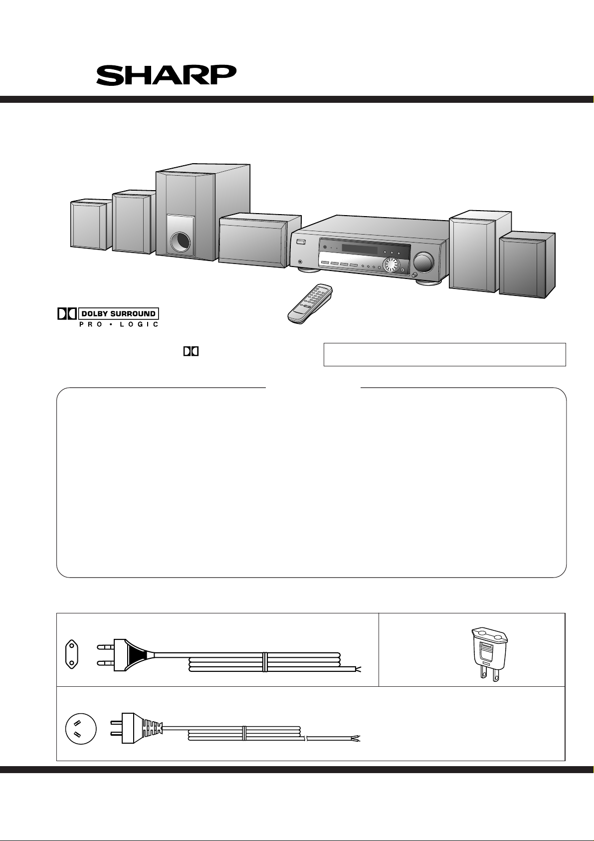
HT-DP2500W
No. S0884HTDP2500
HT-DP2500W
HT-DP2500W home theater system consisting of
HT-DP2500W home theater system, CP-F2500W,
CP-SW2500W, CP-C2500W and CP-SR2500W.
• In the interests of user-safety the set should be restored to its original
condition and only parts identical to those specified should be used.
CONTENTS
Page
AC POWER SUPPLY CORD AND AC PLUG ADAPTOR ...................................................................................................... 1
VOLTAGE SELECTION.......................................................................................................................................................... 2
SPECIFICATIONS ................................................................................................................................................................. 2
NAMES OF PARTS ............................................................................................................................................................... 3
OPERATION MANUAL.......................................................................................................................................................... 4
DISASSEMBLY...................................................................................................................................................................... 6
ADJUSTMENT ...................................................................................................................................................................... 8
NOTES ON SCHEMATIC DIAGRAM .................................................................................................................................... 9
BLOCK DIAGRAM ............................................................................................................................................................... 10
SCHEMATIC DIAGRAM/WIRING SIDE OF P.W.BOARD................................................................................................... 12
TYPES OF TRANSISTOR AND LED.................................................................................................................................... 19
FUNCTION TABLE OF IC.................................................................................................................................................... 24
FL SEGMENT ...................................................................................................................................................................... 28
PARTS GUIDE/EXPLODED VIEW
AC POWER SUPPLY CORD AND AC PLUG ADAPTOR
QACCE0008AW00
OPLGA0250AFZZ
QACCL0005AW00
SHARP CORPORATION
– 1 –
This document has been published to be used
for after sales service only.
The contents are subject to change without notice.
Page 2

SERVICE MANUAL
Manufactured under license from Dolby Laboratories Licensing Corporation.
DOLBY, the double-D symbol and "PRO LOGIC" are
trademarks of Dolby Laboratories Licensing Corporation.
HT-DP2500W
No. S0884HTDP2500
HT-DP2500W
HT-DP2500W home theater system consisting of
HT-DP2500W home theater system, CP-F2500W,
CP-SW2500W, CP-C2500W and CP-SR2500W.
• In the interests of user-safety the set should be restored to its original
condition and only parts identical to those specified should be used.
CONTENTS
Page
AC POWER SUPPLY CORD AND AC PLUG ADAPTOR ...................................................................................................... 1
VOLTAGE SELECTION.......................................................................................................................................................... 2
SPECIFICATIONS ................................................................................................................................................................. 2
NAMES OF PARTS ............................................................................................................................................................... 3
OPERATION MANUAL.......................................................................................................................................................... 4
DISASSEMBLY...................................................................................................................................................................... 6
ADJUSTMENT ...................................................................................................................................................................... 8
NOTES ON SCHEMATIC DIAGRAM .................................................................................................................................... 9
BLOCK DIAGRAM ............................................................................................................................................................... 10
SCHEMATIC DIAGRAM/WIRING SIDE OF P.W.BOARD................................................................................................... 12
TYPES OF TRANSISTOR AND LED.................................................................................................................................... 19
FUNCTION TABLE OF IC.................................................................................................................................................... 24
FL SEGMENT ...................................................................................................................................................................... 28
PARTS GUIDE/EXPLODED VIEW
AC POWER SUPPLY CORD AND AC PLUG ADAPTOR
QACCE0008AW00
OPLGA0250AFZZ
QACCL0005AW00
SHARP CORPORATION
– 1 –
This document has been published to be used
for after sales service only.
The contents are subject to change without notice.
Page 3

HT-DP2500W
FOR A COMPLETE DESCRIPTION OF THE OPERATION OF THIS UNIT, PLEASE REFER
TO THE OPERATION MANUAL.
VOLTAGE SELECTION
The voltage selector is located on the AC voltage selector box. If adjustment is necessary, use a screwdriver in order to turn the
selector in either direction until the correct voltage figure is displayed in the window next to the adjustment screw.
SPECIFICATIONS
HT-DP2500W
● General
Type: Home theater system
Power source: AC 110/127/220/230 - 240 V,
50/60 Hz
Power consumption: 105 W
Dimensions: Width; 430 mm (16-15/16")
Height; 116 mm (4-5/8")
Depth; 322 mm (12-11/16")
Weight: 7.3 kg (16.1 lbs.)
Output power:
(For Australia/
New Zealand)
Output power:
(Except for Australia/
New Zealand)
Output terminals: Front speakers; 8 ohms
Input terminals: VCR-1, VCR-2, AUX (Audio sig-
(Front)
RMS; 50 W (25 W + 25 W)
(10% T.H.D.)
(Centre)
RMS; 25 W (10% T.H.D.)
(Surround)
RMS; 25 W (total) (10% T.H.D.)
(Sub woofer)
RMS; 25 W (10% T.H.D.)
PMPO; 1,000 W
(Front)
RMS; 50 W (25 W + 25 W)
(10% T.H.D.)
(Centre)
RMS; 25 W (10% T.H.D.)
(Surround)
RMS; 25 W (total) (10% T.H.D.)
(Sub woofer)
RMS; 25 W (10% T.H.D.)
Centre speaker; 8 ohms
Surround speakers; 16 ohms
Sub woofer; 8 ohms
Headphones; 16-50 ohms
(recommended; 32 ohms)
nal); 500 mV/47 kohms
CP-F2500W
● Front speaker section
Type: 2-way, 10 cm (4") woofer, and 5
cm (2") tweeter
Maximum input
power: 50 W
Rated input power: 25 W
Impedance: 8 ohms
Dimensions: Width; 150 mm (5-15/16")
Height; 200 mm (7-7/8")
Depth; 125 mm (4-15/16")
Weight: 1.5 kg (3.3 lbs.)/each
CP-C2500W
● Centre speaker section
Type: 10 cm (4") full-range speaker
Maximum input
power: 50 W
Rated input power: 25 W
Impedance: 8 ohms
Dimensions: Width; 200 mm (7-7/8")
Height; 150 mm (5-15/16")
Depth; 125 mm (4-15/16")
Weight: 1.3 kg (2.9 lbs.)
CP-SR2500W
● Surround speaker section
Type: 10 cm (4") full-range speaker
Maximum input
power: 25 W
Rated input power: 12.5 W
Impedance: 16 ohms
Dimensions: Width; 150 mm (5-15/16")
Height; 170 mm (6-3/4")
Depth; 105 mm (4-3/16")
Weight: 1.0 kg (2.2 lbs.)/each
● Tuner section
Frequency range: FM; 88-108 MHz
AM; 531-1,602 kHz
CP-SW2500W
● Sub woofer section
Type: 13 cm (5-1/8") woofer
Maximum input
power: 50 W
Rated input power: 25 W
Impedance: 8 ohms
Dimensions: Width; 210 mm (8-5/16")
Height; 310 mm (12-1/4")
Depth; 310 mm (12-3/16")
Weight: 4.2 kg (9.3 lbs.)
Specifications for this model are subject to change without
prior notice.
– 2 –
Page 4
HT-DP2500W
FOR A COMPLETE DESCRIPTION OF THE OPERATION OF THIS UNIT, PLEASE REFER
TO THE OPERATION MANUAL.
VOLTAGE SELECTION
The voltage selector is located on the AC voltage selector box. If adjustment is necessary, use a screwdriver in order to turn the
selector in either direction until the correct voltage figure is displayed in the window next to the adjustment screw.
SPECIFICATIONS
HT-DP2500W
● General
Type: Home theater system
Power source: AC 110/127/220/230 - 240 V,
50/60 Hz
Power consumption: 105 W
Dimensions: Width; 430 mm (16-15/16")
Height; 116 mm (4-5/8")
Depth; 322 mm (12-11/16")
Weight: 7.3 kg (16.1 lbs.)
Output power:
(For Australia/
New Zealand)
Output power:
(Except for Australia/
New Zealand)
Output terminals: Front speakers; 8 ohms
Input terminals: VCR-1, VCR-2, AUX (Audio sig-
(Front)
RMS; 50 W (25 W + 25 W)
(10% T.H.D.)
(Centre)
RMS; 25 W (10% T.H.D.)
(Surround)
RMS; 25 W (total) (10% T.H.D.)
(Sub woofer)
RMS; 25 W (10% T.H.D.)
PMPO; 1,000 W
(Front)
RMS; 50 W (25 W + 25 W)
(10% T.H.D.)
(Centre)
RMS; 25 W (10% T.H.D.)
(Surround)
RMS; 25 W (total) (10% T.H.D.)
(Sub woofer)
RMS; 25 W (10% T.H.D.)
Centre speaker; 8 ohms
Surround speakers; 16 ohms
Sub woofer; 8 ohms
Headphones; 16-50 ohms
(recommended; 32 ohms)
nal); 500 mV/47 kohms
CP-F2500W
● Front speaker section
Type: 2-way, 10 cm (4") woofer, and 5
cm (2") tweeter
Maximum input
power: 50 W
Rated input power: 25 W
Impedance: 8 ohms
Dimensions: Width; 150 mm (5-15/16")
Height; 200 mm (7-7/8")
Depth; 125 mm (4-15/16")
Weight: 1.5 kg (3.3 lbs.)/each
CP-C2500W
● Centre speaker section
Type: 10 cm (4") full-range speaker
Maximum input
power: 50 W
Rated input power: 25 W
Impedance: 8 ohms
Dimensions: Width; 200 mm (7-7/8")
Height; 150 mm (5-15/16")
Depth; 125 mm (4-15/16")
Weight: 1.3 kg (2.9 lbs.)
CP-SR2500W
● Surround speaker section
Type: 10 cm (4") full-range speaker
Maximum input
power: 25 W
Rated input power: 12.5 W
Impedance: 16 ohms
Dimensions: Width; 150 mm (5-15/16")
Height; 170 mm (6-3/4")
Depth; 105 mm (4-3/16")
Weight: 1.0 kg (2.2 lbs.)/each
● Tuner section
Frequency range: FM; 88-108 MHz
AM; 531-1,602 kHz
CP-SW2500W
● Sub woofer section
Type: 13 cm (5-1/8") woofer
Maximum input
power: 50 W
Rated input power: 25 W
Impedance: 8 ohms
Dimensions: Width; 210 mm (8-5/16")
Height; 310 mm (12-1/4")
Depth; 310 mm (12-3/16")
Weight: 4.2 kg (9.3 lbs.)
Specifications for this model are subject to change without
prior notice.
– 2 –
Page 5
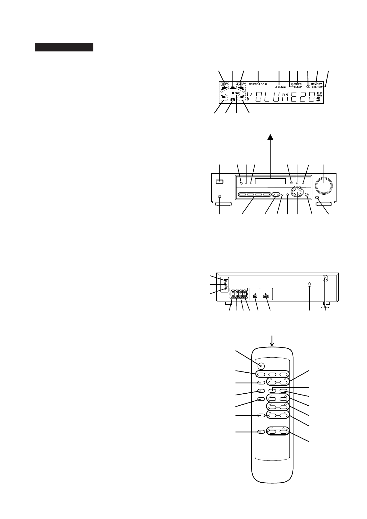
HT-DP2500W
■ Front panel
1. Left Front Speaker Indicator
2. Centre Speaker Indicator
3. Right Front Speaker Indicator
4. Dolby Pro Logic Indicator
5. Extra Bass Indicator
6. Sleep Indicator
7. Timer Play Indicator
8. (TUNER) FM Stereo Indicator
9. (TUNER) Memory Indicator
10. (TUNER) FM Stereo Mode Indicator
11. Left Surround Speaker Indicator
12. Surround Signal Indicator
13. Sub Woofer Indicator
14. Right Surround Speaker Indicator
15. On/Stand-by Button
16. Remote Control Sensor
17. Stand-by Indicator
18. Timer Indicator
19. Dolby Pro Logic Button
20. Equalizer Selector Button
21. Extra Bass Button
22. Volume Control
23. Headphone Socket
24. Function Selector Buttons
25. (TUNER) Tuning Up/Down Buttons
26. Memory Button
27. Timer/Sleep Selector Button
28. Jog Dial
29. Enter Button
30. Sub Woofer Volume Control
NAMES OF PARTS
1
11
1213 14
15
23 24
23 4 56
161718
25
19
26 27 28
HT-DP2500W
8
9
10
7
20 21 22
29
30
■ Rear panel
1. AM Aerial Terminal
2. Aerial Earth Terminal
3. FM 75 Ohms Aerial Terminal
4. VCR-1 Output Sockets
5. VCR-1 Input Sockets
6. VCR-2 Input Sockets
7. AUX Input Sockets
8. Surround Speaker Sockets
9. Front/Centre/Sub Woofer Sockets
10. AC Voltage Selector
11. AC Power Lead
■ Remote control
1. Remote Control Transmiter LED
2. On/Stand-by Button
3. Function Selector Buttons
4. Preset Balance Button
5. Dolby Pro Logic Button
6. Test Tone Button
7. Tuner Call Button
8. Mute Button
9. Balance Selector Buttons
10. Equalizer Selector Button
11. Extra Bass Button
12. Centre Level Buttons
13. Surround Level Buttons
14. (TUNER) Preset Up/Down Buttons
15. Volume Control Buttons
1
2
3
4
5
67
8
9
10
11
1
2
3
4
5
6
7
8
9
10
11
12
13
14
15
– 3 –
Page 6
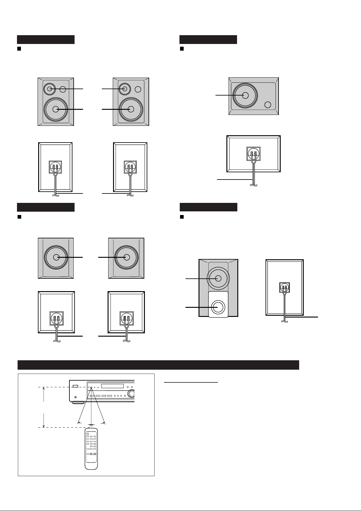
HT-DP2500W
CP-F2500W
Front Speaker
1. Tweeter
2. Woofer
3. Speaker Cord
CP-SR2500W
Surround Speaker
1. Woofer
2. Speaker Cord
CP-C2500W
Center Speaker
1. Woofer
2. Speaker Cord
1
1
2
2
3
CP-SW2500W
Sub woofer
1. Woofer
2. Bass Reflex Duct
3. Speaker Cord
1
2
PREPARATION FOR USE
0.2 m - 6 m
(8" - 20')
15˚
15˚
1
2
OPERATION MANUAL
■
Remote control
Notes concerning use:
● Replace the batteries if the operating distance is reduced
or if the operation becomes erratic.
● Periodically clean the transmitter LED on the remote control and the sensor on the main unit with a soft cloth.
● Exposing the sensor on the main unit to strong light may
interfere with operation. Change the lighting or the direction of the unit.
● Keep the remote control away from moisture, excessive
heat, shock, and vibrations.
3
– 4 –
Page 7

HT-DP2500W
CP-F2500W
Front Speaker
1. Tweeter
2. Woofer
3. Speaker Cord
CP-SR2500W
Surround Speaker
1. Woofer
2. Speaker Cord
CP-C2500W
Center Speaker
1. Woofer
2. Speaker Cord
1
1
2
2
3
CP-SW2500W
Sub woofer
1. Woofer
2. Bass Reflex Duct
3. Speaker Cord
1
2
PREPARATION FOR USE
0.2 m - 6 m
(8" - 20')
15˚
15˚
1
2
OPERATION MANUAL
■
Remote control
Notes concerning use:
● Replace the batteries if the operating distance is reduced
or if the operation becomes erratic.
● Periodically clean the transmitter LED on the remote control and the sensor on the main unit with a soft cloth.
● Exposing the sensor on the main unit to strong light may
interfere with operation. Change the lighting or the direction of the unit.
● Keep the remote control away from moisture, excessive
heat, shock, and vibrations.
3
– 4 –
Page 8
(Continued)
■
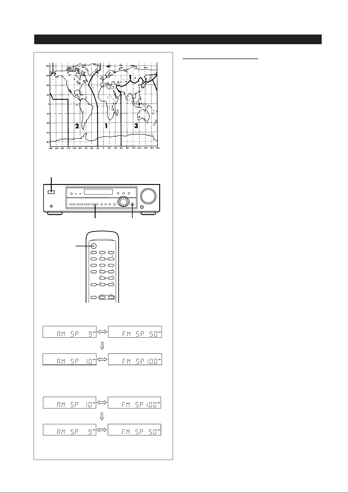
AM/FM Interval (span)
The International Telecommunication Union (ITU) has established that member countries should maintain either a 10
kHz or a 9 kHz interval between broadcasting frequencies
of any AM station. The illustration shows the 9 kHz interval
zones (regions 1 and 3), and the 10 kHz interval zone (region
2).
This product is not equipped with a span selector. However,
it will be adjusted to 9 kHz AM interval (50 kHz FM interval)
when shipped from the factory.
Before using the unit, be sure to set it for the AM tuning
interval (span) used in your area.
To check the tuning span currently selected:
1
Set the ON/STAND-BY button on the main unit to ON.
2
Press the TUNER (BAND) button until "FM" or "AM" appears in the display.
3
Press the TUNER (BAND) button to select the AM band.
● If "AM 531 kHz" is displayed, it means that the radio has
been adjusted for a 9 kHz span. If "AM 530 kHz" is displayed, it means that the radio has been adjusted for a
10 kHz span.
To change from a 9 kHz AM (50 kHz FM) interval to a
10 kHz AM (100 kHz FM) interval:
1
Press the ON/STAND-BY button on the remote control
to enter the stand-by mode.
2
Hold down the TUNER (BAND) button and the ENTER
button for at least 4 seconds. Release the buttons when
"AM SP 10 kHz" and "FM SP 100 kHz" are displayed
alternately.
To return to a 9 kHz AM (50 kHz FM) interval:
1
Press the ON/STAND-BY button on the remote control
to enter the stand-by mode.
2
Hold down the TUNER (BAND) button and the ENTER
button for at least 4 seconds. Release the buttons when
"AM SP 9 kHz" and "FM SP 50 kHz" are displayed alternately.
Caution:
● When the unit is left for a few hours after the span has
been switched and AC power lead disconnected, it will
be automatically returned to a 9 kHz span. If this happens, set the span again.
● When the span is switched, any stations that are
memorised will be cancelled.
ON/STAND-BY
TUNER (BAND)
ENTER
ON/
STAND-BY
[9 kHz → 10 kHz]
(4 seconds)
[10 kHz → 9 kHz]
(4 seconds)
HT-DP2500W
– 5 –
Page 9
HT-DP2500W
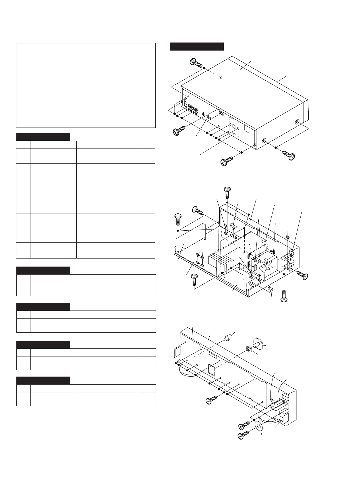
DISASSEMBLY
Caution on Disassembly
Follow the below-mentioned notes when disassembling
the unit and reassembling it, to keep it safe and ensure
excellent performance:
1. Be sure to remove the power supply plug from the wall
outlet before starting to disassemble the unit.
2. Take off nylon bands or wire holders where they need be
removed when disassembling the unit. After servicing
the unit, be sure to rearrange the leads where they were
before disassembling.
3. Take suff cient care on static electricity of integrated
circuits and other circuits when servicing.
HT-DP2500W
(A1)x2
ø3x10mm
Top Cabinet
Front Panel
HT-DP2500W
REMOVAL PROCEDURESTEP FIGURE
1 Top Cabinet 1. Screw ................. (A1) x5 6-1
2 Rear Panel 1. Screw ............... (B1) x11 6-1
3
Front Panel
4 Main PWB/ 1. Screw .................(D1) x7 6-2
Tuner PWB 2. Socket ................(D2) x3
5 Power Supply PWB 1. Screw ................. (E1) x5 6-2
(With Voltage Selector
Switch PWB)
6 Display PWB 1. Knob ................... (F1) x1 6-3
7 Switch PWB 1. Screw ................ (G1) x2 6-3
8
Headphones PWB
1. Screw .................(C1) x5 6-2
2. Flat Cable ...........(C2) x1
3. Socket ................(C3) x3
2. Socket ................ (E2) x3
2. Nut ...................... (F2) x1
3. Screw ............... (F3) x10
4. Socket ................ (F4) x1
5. Knob ................... (F5) x1
1. Screw ................ (H1) x1 6-3
CP-F2500W
STEP
1 Speaker 1. Net ........................(A1) x1 7-1
REMOVAL
PROCEDURE
2. Screw ....................(A2) x6
CP-SW2500W
STEP
1 Speaker 1. Net ........................(A1) x1 7-2
REMOVAL PROCEDURE
2. Screw ....................(A2) x4
FIGURE
FIGURE
(A1)x1
ø3x10mm
Voltage Selector
Switch PWB
(D1)x3
ø3x8mm
Tuner
PWB
Main
PWB
(E1)x5
ø3x8mm
Display PWB
Rear
Panel
(C1)x1
ø3x8mm
(D2)x2
Front Panel
Figure 6-1
(D1)x4
(C3)x1
ø3x8mm
(E2)x1
Power Supply
PWB
Figure 6-2
(F5)x1
(B1)x11
ø3x10mm
(C2)x1
(A1)x2
ø3x10mm
Front Panel
Power Amp. PWB
Headphones
(E2)x2
(C3)x1
PWB
(D2)x1
(C3)x1
(C1)x3
ø3x8mm
(C1)x1
ø3x8mm
CP-C2500W
STEP REMOVAL PROCEDURE
1 Speaker 1. Net ........................(A1) x1 7-3
2. Screw ....................(A2) x4
CP-SR2500W
STEP
1 Speaker 1. Net ........................(A1) x1 7-4
REMOVAL
PROCEDURE FIGURE
2. Screw ....................(A2) x4
FIGURE
– 6 –
(F3)x10
ø3x10mm
(H1)x1
ø3x10mm
(F1)x1
(F2)x1
(F4)x1
Switch PWB
(G1)x2
ø3x10mm
HeadphonesPWB
PWB Washer
Figure 6-3
Page 10
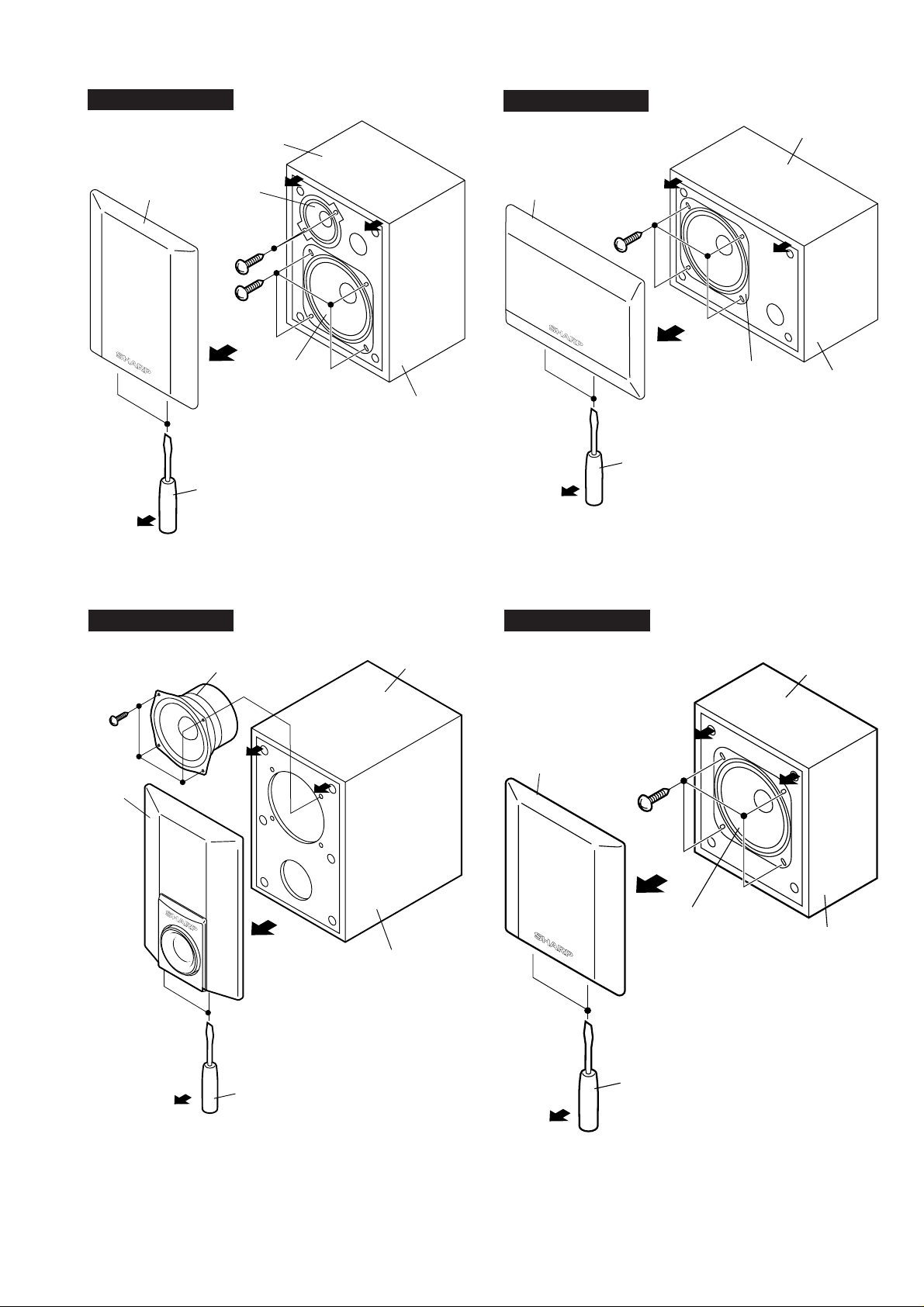
HT-DP2500W
Screw
Driver
(A1)x1
(A2)x4
ø4x13mm
Speaker Box
Woofer
Top Side
CP-F2500W
(A1)x1
Top Side
Tweeter
(A2)x2
ø4x13mm
(A2)x4
ø4x13mm
Screw
Driver
Figure 7-1
CP-C2500W
Woofer
Speaker Box
Figure 7-3
CP-SW2500W
(A2)x4
ø4x13mm
(A1)x1
Woofer
Top Side
Speaker Box
CP-SR2500W
(A1)x1
Top Side
(A2)x4
ø4x13mm
Woofer
Speaker Box
Screw
Driver
Figure 7-2
Screw
Driver
Figure 7-4
– 7 –
Page 11
HT-DP2500W
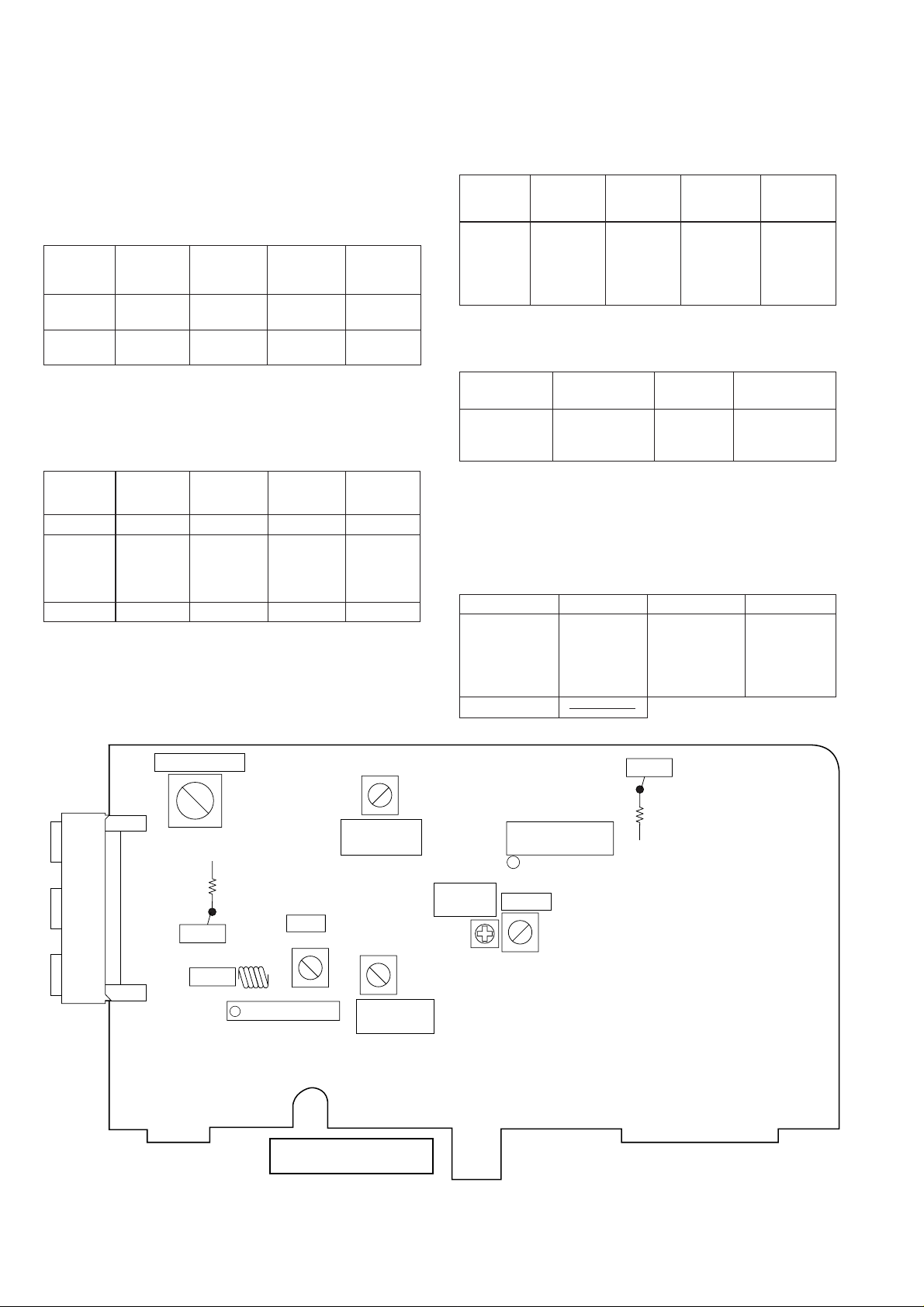
ADJUSTMENT
TUNER SECTION
fL: Low-range frequency
fH: High-renge frequency
• FM RF
Signal generator: 1 kHz, 75 kHz dev., FM modulated
Test Stage
Band — 87.50 kHz (fL): L202 *1
Coverage 3.4 ± 0.1 V
RF 98 MHz 98.00 MHz L201 *2
Frequency
(10 - 30 dB)
Frequency
Display
*1. Input: Antenna, Output: TP302
*2. Input: Anetnna, Output: Speaker Terminal
• AM IF/RF
Signal generator: 400 Hz, 30%, AM modulated
Test Stage
IF 450 kHz 1,602 kHz T204 *1
Band — 531 kHz (fL): T203 *2
Tracking 990 kHz 990 kHz T201 *1
Frequency
Frequency
Display
*1. Input: Antenna, Output: TP301
*2. Input: Input is not connected, Output: TP302
Setting/
Adjusting
Parts
Setting/
Adjusting
Parts
(AM Band
Coverage
0.8V±0.1v
Instrument
Connection
Instrument
Connection
• FM Detection
Signal generator: 10.7 MHz, FM sweep
Test Stage
IF 10.7 MHz 98.00 MHz T202 Input: Pin 1
Frequency
Frequency
Display
Setting/
Adjusting
Parts
(Turn the of IC201
core of T202 Output:
fully counter- Pin 1of
clockwise) IC203
Instrument
Connection
• FM Mute Level
Signal generator: 1 kHz, 40 kHz dev., FM modulated
Frequency Adjusting
98.0 MHz 98.00 MHz VR201 *1 Input: SOC201
(25 dBµV) Output: Speaker
Frequency
Display
Parts
Instrument
Connection
Terminal
*1. Adjust so that an output signal appears.
• Setting the Test Mode
Keeping the ENTER button and MEMORY button pressed,
turn on POWER (of Main Set). Then, the frequency is initially
set in the memory as shown in Table. Call it with the JOG to
use it for adjustment and check of tuner circuit.
Preset No.
1 87.50 MHz 6 531 kHz
2 108.00 MHz 7 1,602 kHz
3 98.00 MHz 8 990 kHz
4 90.00 MHz 9 603 kHz
5 106.00 MHz 10 1,404 kHz
11~40
FM Preset No.
AM
SOC201
ANTENNA
TERMINAL
AM TRACKING
T201
R216
TP302
FM RF
1
FM IF
T202
L201
IC201
TUNER PWB
T203
VR201
24
1
AM IF
T204
AM BAND
COVERAGE
FM MUTE
LEVEL
L202
FM BAND
COVERAGE
Figure 8 ADJUSTMENT POINTS
IC203
TP301
R223
13
12
– 8 –
Page 12

HT-DP2500W
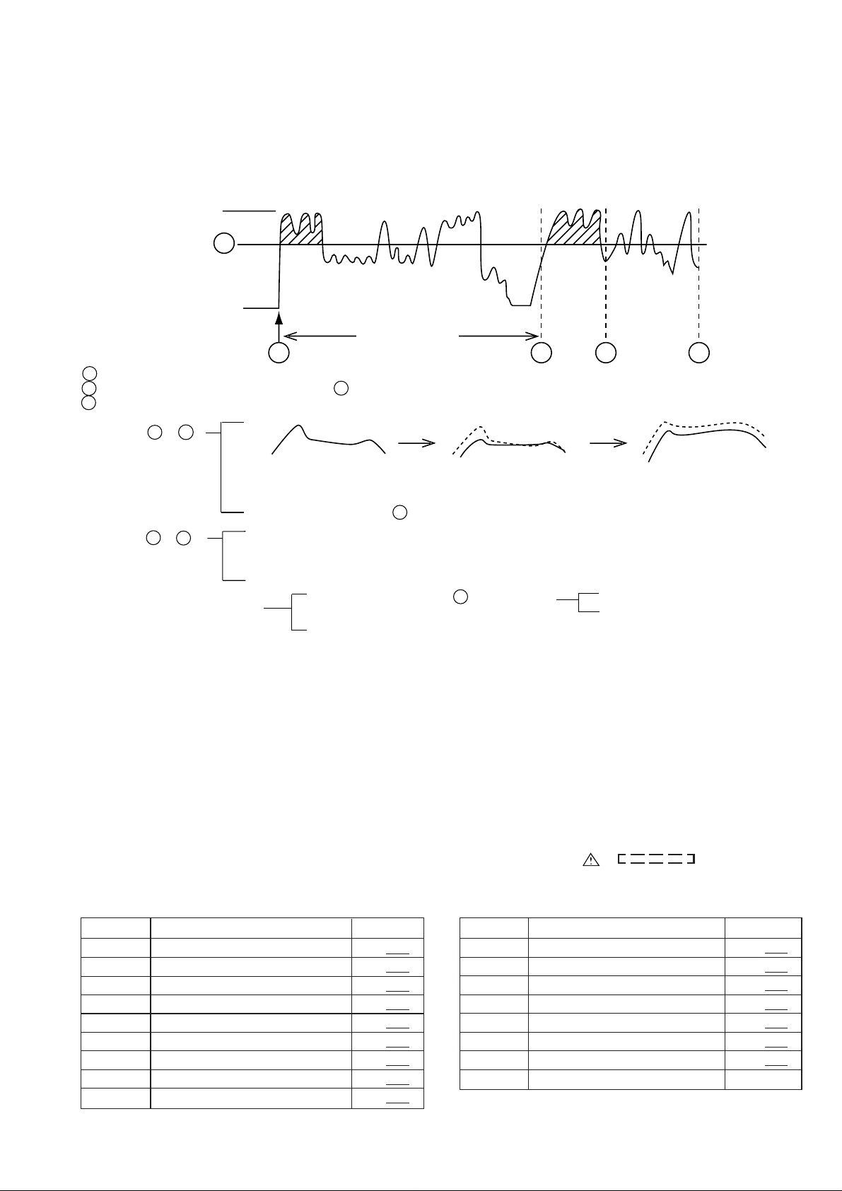
EXPLANATION OF AUTOMATIC SOUND VALUE CORRECTION CONTROL
1. Outline
The recent trend is toward rise of CD record level in the world, for example rock, dancing music, etc. In case of continuous high
level playback G-EQ (graphic equalizer) and VOL (Volume) are controlled (lowered) automatically after a lapse of specific time
(10 minutes) so as to get the easy-to-listen sound level.
2. Explanation of operation
The CD playback operation is explained below.
Distortion clip point
X
0w
10 minutes
A
X
: Threshold value of control circuit operation
A : Hight energy (hatched area) exceeding X is detecated, and the control mode is set.
B : After a lapse of 10 minutes the control is started.
B ~ C :
Data is fetched every 4
seconds to control.
C ~ D :
Control mode cancel conditions
Initial frequency
characteristics.
If hight energy exceeding X is detected, VOL is lowered to get sound easy to listen.
Stable control
Continued control
The output data is fetched every 4 seconds to control. When quiet music is played back, the
control is performed so as to restore the initial frequency characteristics and initial VOL values.
When output exceeding X is not given
continuously for 10 minutes.
When the power is turned off or on.
Hand L frequency characteristics are lowered.
B C D
SP output
level
VOL (Volume) is lowered.
When quiet music is played back.
When VOL is lowered.
NOTES ON SCHEMATIC DIAGRAM
• Resistor:
To differentiate the units of resistors, such symbol as K and
M are used: the symbol K means 1000 ohm and the symbol
M means 1000 kohm and the resistor without any symbol is
ohm-type resistor. Besides, the one with “Fusible” is a fuse
type.
• Capacitor:
To indicate the unit of capacitor, a symbol P is used: this
symbol P means micro-micro-farad and the unit of the
capacitor without such a symbol is microfarad. As to electrolytic capacitor, the expression “capacitance/withstand voltage” is used.
(CH), (TH), (RH), (UJ): Temperature compensation
(ML): Mylar type
(P.P.): Polypropylene type
SW1 ON STAND-BY ON—OFF
SW2 TIMER/SLEEP ON—OFF
SW3 DOLBY PRO LOGIC ON—OFF
SW4 EQUALIZER ON—OFF
SW5 X-BASS ON—OFF
SW6 ENTER ON—OFF
SW7 VOLUME DOWN ON—OFF
SW8 VOLUME UP ON—OFF
SW9 MEMORY/SET ON—OFF
• Schematic diagram and Wiring Side of P.W.Board for this
model are subject to change for improvement without prior
notice.
• The indicated voltage in each section is the one measured by
Digital Multimeter between such a section and the chassis
with no signal given.
1. In the tuner section,
( ) indicates AM
< > indicates FM stereo
2. In the main section, VCR1.
3. In the power section, VCR1.
• Parts marked with “ ” ( ) are important for
maintaining the safety of the set. Be sure to replace these
parts with specified ones for maintaining the safety and
performance of the set.
POSITIONREF. NO DESCRIPTIONREF. NO DESCRIPTION POSITION
SW10 TUNING UP ON—OFF
SW11 TUNING DOWN ON—OFF
SW12 TUNER(BAND) ON—OFF
SW13 CD/AUX ON—OFF
SW14 VCR-2 ON—OFF
SW15 VCR-1 ON—OFF
SW23 JOG DIAL ON—OFF
SW601 VOLTAGE SELECTOR 110V
– 9 –
Page 13
HT-DP2500W
EXPLANATION OF AUTOMATIC SOUND VALUE CORRECTION CONTROL
1. Outline
The recent trend is toward rise of CD record level in the world, for example rock, dancing music, etc. In case of continuous high
level playback G-EQ (graphic equalizer) and VOL (Volume) are controlled (lowered) automatically after a lapse of specific time
(10 minutes) so as to get the easy-to-listen sound level.
2. Explanation of operation
The CD playback operation is explained below.
Distortion clip point
X
0w
10 minutes
A
X
: Threshold value of control circuit operation
A : Hight energy (hatched area) exceeding X is detecated, and the control mode is set.
B : After a lapse of 10 minutes the control is started.
B ~ C :
Data is fetched every 4
seconds to control.
C ~ D :
Control mode cancel conditions
Initial frequency
characteristics.
If hight energy exceeding X is detected, VOL is lowered to get sound easy to listen.
Stable control
Continued control
The output data is fetched every 4 seconds to control. When quiet music is played back, the
control is performed so as to restore the initial frequency characteristics and initial VOL values.
When output exceeding X is not given
continuously for 10 minutes.
When the power is turned off or on.
Hand L frequency characteristics are lowered.
B C D
SP output
level
VOL (Volume) is lowered.
When quiet music is played back.
When VOL is lowered.
NOTES ON SCHEMATIC DIAGRAM
• Resistor:
To differentiate the units of resistors, such symbol as K and
M are used: the symbol K means 1000 ohm and the symbol
M means 1000 kohm and the resistor without any symbol is
ohm-type resistor. Besides, the one with “Fusible” is a fuse
type.
• Capacitor:
To indicate the unit of capacitor, a symbol P is used: this
symbol P means micro-micro-farad and the unit of the
capacitor without such a symbol is microfarad. As to electrolytic capacitor, the expression “capacitance/withstand voltage” is used.
(CH), (TH), (RH), (UJ): Temperature compensation
(ML): Mylar type
(P.P.): Polypropylene type
SW1 ON STAND-BY ON—OFF
SW2 TIMER/SLEEP ON—OFF
SW3 DOLBY PRO LOGIC ON—OFF
SW4 EQUALIZER ON—OFF
SW5 X-BASS ON—OFF
SW6 ENTER ON—OFF
SW7 VOLUME DOWN ON—OFF
SW8 VOLUME UP ON—OFF
SW9 MEMORY/SET ON—OFF
• Schematic diagram and Wiring Side of P.W.Board for this
model are subject to change for improvement without prior
notice.
• The indicated voltage in each section is the one measured by
Digital Multimeter between such a section and the chassis
with no signal given.
1. In the tuner section,
( ) indicates AM
< > indicates FM stereo
2. In the main section, VCR1.
3. In the power section, VCR1.
• Parts marked with “ ” ( ) are important for
maintaining the safety of the set. Be sure to replace these
parts with specified ones for maintaining the safety and
performance of the set.
POSITIONREF. NO DESCRIPTIONREF. NO DESCRIPTION POSITION
SW10 TUNING UP ON—OFF
SW11 TUNING DOWN ON—OFF
SW12 TUNER(BAND) ON—OFF
SW13 CD/AUX ON—OFF
SW14 VCR-2 ON—OFF
SW15 VCR-1 ON—OFF
SW23 JOG DIAL ON—OFF
SW601 VOLTAGE SELECTOR 110V
– 9 –
Page 14
HT-DP2500W
A
1
FM
GND
AM
SOC201
ANTENNA
TERMINAL
BAND PASS
FILTER
1 2 3
BF201
IC201
1
FM FRONT END
TA7358AP
2
6
5
3
4
L201
FM RF
T202
FM IF
AM RF
AM ANTENNA
T201
7
VT
OSC
FM OSC
T203
8
FM IF
L202
AM OSC.
9
FM IF
AMP
Q201
IF AMP
Q281
FM MUTE LEVEL
FMOSC
VT
A+12V
FM +B
Q203
VR201
FM
FM IF
CF201
AM IF
FM IF IN
1
AM MIX
FM IF
IN
AM
AM
OSC
OSC
24
23
OUT
X202
4.5MHz
20
1
X IN X OUT
A OUT
OSC
7
BO 1
PLL CONTROLLER
+B3
CF202
AM IF
6
SD
4
FM IF
5
GND
10
IF OUT
AM IF
CF203
T204
2
3
REQ
OUT
IC203 LA1833
FM IF DET./FM MPX./AM IF
22
21
AFC
7
STEREO
AM RF IN
IN
STEREO
VOLTAGE
REGURATER
A+12V
+B3
IF IN
IO1
FM IN
AM IN
22
16
11
15
IC202
LC72131
3
12
VSS
21
4
6
5
DICLCE
DO
8 9
FM
DET
VDD
+B3
VCC
11
PHASE
+5V
17
BO4
FM
+B3
10
9
17 18
FM
OUT
12
AM/FM
MPX
VCO
CUT
OUT
L CH
L-CH
19 16
AM
MPX
IN
R CH
14 13
R-CH
15
MUTING
Q202
TUNER
MUTE
VPP
P15
P11
P14
P13
P10
P12
7 6 5 4
11 10
9
8
73 74
75
P13
76
P11
P10
P12
P14
77
78
P15
79
P16
80
NC
81
NC
82
NC
83
NC
84
DAPD
85
ADPD
86
AC3-RES
87
AC3-SS
AC3-SI
88
89
D-SEL
AC3-SCK
90
SW-ON
91
PRO-EN
92
PRO-DI
93
PRO-CK
94
V-SW1
95
V-SW2
96
V-MUTE
97
NC
98
NC
99
TUN-DO
TUN-DI
TUN-CK
100
1 2 3
F1
NC(NP)
F1
P16
NC(NP)
1
3
2
VP
(AC)
SD
Q5
JK401
AUDIO
INPUT/OUTPUT
TERMINALS
VCR1
IN
VCR1
OUT
VCR2
IN
AUX
IN
L-CH
R-CH
L-CH
R-CH
L-CH
R-CH
L-CH
R-CH
MUTE
MUTING
Q411
Q412
IC411
NJM4565D
VCR1 OUTPUT AMP.
IC411
AMP
L-CH
2
R-CH
6
4
8
A–12V A+12V
A+12V
L-CH
3
5
R-CH
VCR1
VCR2
TUNER
AUX
L-CH
R
L-CH
R
L-CH
R-CH
L-CH
R-CH
34
CLK
38
35
DATA
37
ENABLE
36
18
VCC
8
VREF
7
21
GND
X451
8MHz
DICECL
232425
55
L1
57
R1
L2
54
58
R2
L4
52
R4
60
L3
53
R3
59
FRONT
IN
48
64
RT IN
LT IN
L-IN
IC452
LV1035M
DOLBY
PRO LOGIC
DECORDER
OSC
31
32
A+12V
56
VDD
IC501 LC75396N
AUDIO PROCESSOR
GRAPHIC EQUALIZER
VSS
LF1C1
R-IN
RF1C1
47
1
26
R
L
C-OUT
C-OUT
9
24
L-OUT
23
R-OUT
22
S-OUT
S-IN
16
10 11
46 45
LT-IN
R-OUT
S-OUT
LSELO
RSELO
6349
L-CHOUT
R-IN
RT-IN
L-OUT
14
12
R-CHOUT
L-IN
15
44
4
LF2C1
RF1C2
LF1C2
46
2
R
L
X-BASS
L-MIX OUT
R-MIX OUT
S-OUT
HEAVY
SOFT
34
43 42
5
LF2C2
RF2C1
RF2C2
LFOUT
CENTER
REAR IN
RF1C3
LF1C3
RRIN LRIN
30
1845
3
R
L
S-IN
C-IN
LF2C3
VOLUME
VOLUME
HEADPHONE AMP.
H-MUTE
33
16
LFIN
L-CH
31
LFOUT
RFCOM
17
R-CH
RFOUT
REAR
OUT
RROUT
20
28
LROUT
CENTER
OUT
IC581
NJM4558D
A+12V
IN
8
L-CH
3
5
R-CH
A–12V
IC561
NJM4558D
BUFFER
REAR
IN
5
3
CENTER
4
8
4
Q531
Q532
A–12V
1
IN
6
4
A–12V
IC431
NJM4558D
LOW PASS FILTER
AMP.
OUT
L-CH
1
7
R-CH
J581
HEADPHONES
A+12V
REAR
OUT
7
1
CENTER
SUB WOOFER
2
OUT
J581
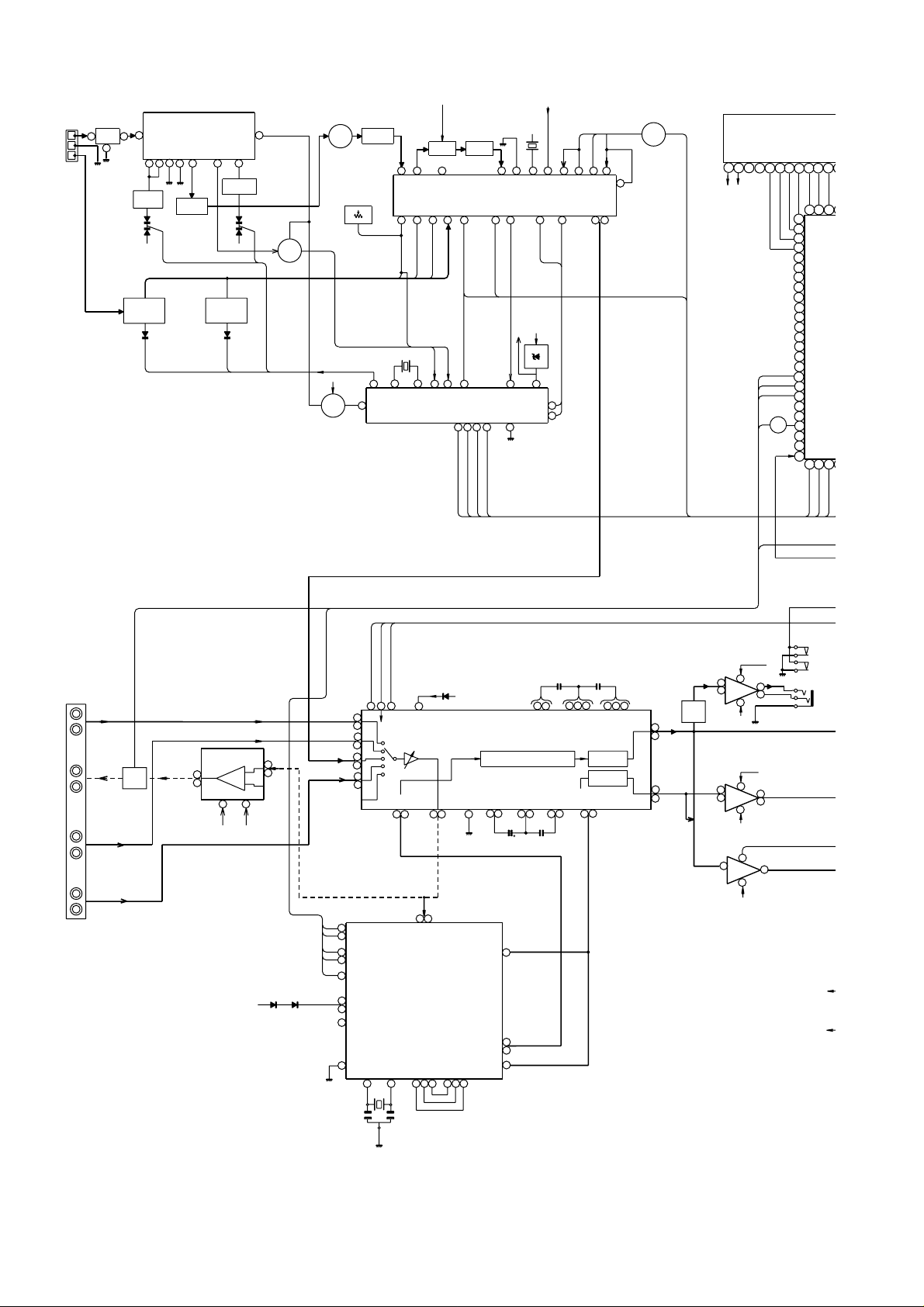
Figure 10 BLOCK DIAGRAM (1/2)
– 10 –
Page 15

HT-DP2500W
P13
J
FL1
FL DISPLAY
P1
P2
P11
P13
P10
P12
12
13
11 10
9
8
72
71
73 74
75
76
P11
P10
P12
77
78
P15
79
P16
80
NC
81
NC
82
NC
83
NC
84
DAPD
85
ADPD
86
AC3-RES
87
AC3-SS
AC3-SI
88
89
D-SEL
AC3-SCK
90
SW-ON
91
PRO-ENA
92
PRO-DI
93
PRO-CK
94
V-SW1
95
V-SW2
96
V-MUTE
97
98
99
100
1 2 3 4
TUN-DI
TUN-DO
TUN-CK
TUN-CE
TUN-MUTE
5 6 7
P3P4P5P6P7P8P9
10G
25 20
18
15 14
17 16
19
63 64
66
69 70
67 68
65
P1
P2
P3P4P5P6P7P8P9
10G
IC1
IX0001SJ
SYSTEM
MICROCOMPUTER
TUN-SD
TUN-ST
VDD
OSC2
OSC1
VSS XIXO
MMOD
11 12
32.768kHz
13 14
XL1
15
VREF
8 9
XL2
8MHz
10
3G4G5G6G7G8G9G
1G
2G
NC(NC)
NC(NC)
NC(NC)
NC(NC)
24
FAN
SPSWB
SPSWA
LED1
V-CK
FS-CK
FS-STB
RESET
24
NC
VREF+
Q10
51 52
NC
25
ALC
35
PROTECT
50
49
48
47
46
45
44
43
42
41
40
39
38
37
36
35
34
33
32
31
30
29
28
27
26
21 22 23
KEY2
34 33 32 31
30
54 55 56 57
58
18
KEY3
19
AREA
20
2G
3G4G5G6G7G8G9G
JOG DOWN
REMOCON
SYS-STOP
SP-LEVEL
MODEL
22 23
21
53
1G
SW-RLAY
C-RLAY
R-RLAY
POW-SW
FA-RLAY
SW-MUTE
C-MUTE
R-MUTE
F-MUTE
JOG UP
AC3-SO
POWER
V-DATA
V-LACH
FS-DATA
POSISTER
29
28 27 26
59
60 61 62
KEY1
17
16
NC(NP)
36
NC(NP)
VF1
(AC)
F2
F2
38 37
FAN
Q1
LED1
STAND-BY LED
LED2
TIMER LED
SW23
SW1
JOG
ON
DIAL
STAND-BY
VF2
(AC)
Q11
Q12
Q4
Q3
Q2
Q13
REMOCON
RESET
Q6
L-CH IN
F-MUTE
R-CH IN
581
Q632
Q633
RX1
1
REMOTE
SENSOR
2
10
IC701
LM2876
POWER AMP.
1
–B1
+B1
5
4
7
Q701
Q702
10
IC702
LM2876
POWER AMP.
1
–B1
+B1
5
4
7
3
8
8
M671
M
FAN MOTOR
SW2-SW8
SW9-SW15
KEY MATRIX
Q7
Q8
ZD1
SWITCHING
OVER CURRENT
DETECTOR
L-CH OUT
3
OVER CURRENT
DETECTOR
R-CH OUT
3
SWITCHING
µ-COM+5V
Q707
Q708
Q705
Q706
Q755
Q756
SO701
SPEAKER
TERMINALS
FRONT
+
L-CH
–
GND
FRONT
+
R-CH
GND
–
8
8
8
OVER CURRENT
DETECTOR
SUB WOOFER OUT
3
SWITCHING
OVER CURRENT
DETECTOR
CENTER OUT
3
SWITCHING
OVER CURRENT
DETECTOR
REAR-OUT
3
T601
POWER
TRANSFORMER
Q785
Q786
Q784
T.F
T100mA L 250V
Q754
Q775
Q776
Q774
SW601
VOLTAGE
SELECTOR
F603
SUB WOOFER
+
–
GND
+
CENTER OUT
–
GND
S0702
REAR
SPEAKER
TERMINALS
+
L-CH
GND
–
GND
–
R-CH
+
AC POWER
SUPPLY CORD
F601
AC110/127/
220/230-240V
T2.5A L 250V
50/60Hz
LF601
LINE FILTER
ONES
VR1
SUB-WOOFER
VOLUME
OOFER
230-240V/
220V
VOLTAGE
REGURATER
D630
A-12V
A+12V(ANALOG)
VF2
(AC)
Q621
Q622
VP
VF1
(AC)
D621-D624
VOLTAGE
REGULATOR
Q611
F611
T800mA L 250V
127V
110V
T.F
T602
POWER
TRANSFORMER
SWITCHING
POWER SW
µ-COM5V
T1.25A L 250V
POW-2
Q603
Q602
S/W IN
S-MUTE
CENTER IN
C-MUTE
REAR-IN
R-MUTE
F602
RLY601
VOLTAGE
REGULATOR
Q601
10
IC703
LM2876
POWER AMP.
1
–B1
+B1
5
4
7
Q751
Q752
10
IC704
LM2876
POWER AMP.
1
–B1
+B1
5
4
7
Q771
Q772
10
IC705
LM2876
POWER AMP.
1
–B1
+B1
5
4
7
Q781
Q782
POW-1
D601–D604
Figure 11 BLOCK DIAGRAM (2/2)
– 11 –
Page 16

HT-DP2500W
1K
N
E
E
E
U
U
U
U
U
/
N
/
D
S
S
RF4C2
8
6
A
B
C
D
E
F
G
H
L-CH
VCR-1
IN
R-CH
L-CH
VCR-1
OUT
R-CH
JK401
AUDIO
INPUT/
OUTPUT
TERMINALS
L-CH
VCR-2
IN
R-CH
L-CH
AUX
IN
R-CH
CNP201
12
11
10
9
8
FC1
R403
4.7K
R404
4.7K
R419
2.2K
V_MUTE
23
1
CNS1B
C407
2.2/50
R407
22K
R408
22K
C408
2.2/50
7
6
5
4
3
2
1
23
22
21
20
19
18
17
16
15
14
13
12
11
10
9
8
7
6
5
4
3
2
1
R409
5.6K
R410
5.6K
TO TUNER PWB
CNP1A
TO DISPLAY PWB
P16 1-F
R401
33K
C401
390P
C402
390P
R402
33K
Q411
R405
2SC2878 B
1K
0V
C405
330P
0V
C406
330P
0V
R406
Q412
1K
2SC2878 B
MUTING
R421
33K
C421
390P
C422
390P
R422
33K
R425
33K
C423
390P
C424
390P
R426
33K
C425
0.022
D421
D422
1N4148
1N4148
CNS201
P18 5-A
MUTING
VCR-1:( )
0V
(0.7V)
0V
R420
2.2K
R423
4.7K
R424
4.7K
R427
4.7K
R428
4.7K
(0.7V)
MAIN PWB-A1(1/2)
TUN_CK
TUN_DO
TUN_CE
TUN_DI
D_GND
TUN_SD
TUN_ST
TUN_MUTE
A+12V
TUN_R
A_GND
TUN_L
FUN_SW
PROTECT
H/P_SW
SW_MUTE
C_MUTE
R_MUTE
F_MUTE
V_DATA
V_CK
V_LATCH
POSISTOR
SP_LEVEL
TUN_ST
TUN_SD
TUN_MUTE
TUN_CE
TUN_CK
TUN_DI
TUN_DO
V_MUTE
PRO_CK
PRO_DI
PRO_ENA
IC411
NJM4565D
VCR 1 OUTPUT AMP.
C411
C409
47P
R411
18K
R412
18K
C410
47P
47P
0V10V
R413
5.6K
0V
IC411
NJM4565D
8
6
7
0V
0V
R414
5.6K
C412
47P
–9.7V
0V
4 3 2 1
5
0V
FM SIGNAL
AUDIO SIGNAL
R416
4.7K
R417
8.2K
R415
4.7K
R418
8.2K
C413
2.2/50
C415
0.022
C437
47/16
C416
C414
+B
0.022
2.2/50
+B
C438
47/16
R449
220
R448
220
C485
4.7/50
C487
4.7/50
C489
3.3/50
C491
0.15/50
C493
0.15/50
C495
0.47/50
R480
C484
0.47/50
C486
0.47/50
C488
0.15/50
C490
0.15/50
C492
3.3/50
C494
4.7/50
C496
4.7/50
C497
0.47/50
C515
1/50
C511
47/16
C509 1/50
C507 1/50
C505 1/50
C503 1/50
C501 1/50
C502 1/50
C504 1/50
C506 1/50
C508 1/50
C510 1/50
C512
47/16
C516
1/50
1K
R503
27K
R501
3.9K
R502
C514
100P
R479
1K
3.9K
C453
0.1
4.7V
L-BPF3
4.7V
5.4V
4.8V
5.4V
4.7V
4.7V
4.7V
4.7V
4.7V
4.7V
5.4V
4.7V
5.4V
4.7V
4.7V
C454
0.1
R519 1K
R517 1K
R515 1K
R513 1K
R511 1K
R512 1K
R514 1K
R516 1K
R518 1K
R520 1K
49
50
51
52
53
54
55
56
57
58
59
60
61
62
63
64
C550
330/16
C455
0.1
4.7V
L-BPF2
DC-OUT3
R-RECT
DC-OUT4
L-RECT
VLR-TH
VLR-1
VLR-2
VCR-2
VCR-1
VCR-TH
L+R-RECT
DC-OUT2
L-R-RECT
DC-OUT1
R-BPF3
4.7V
R-BPF2
C456
0.1
100P
C513
+B
27K
R504
4.6V
4.6V
R-BPF1
C549
D501
D502
C480
C483
47/50
4.5V
4.5V
4.7V
4.8V
L-BPF1
LT-IN
RT-IN
DC-OUT
C-MODE
LV1035M
DOLBY PRO LOGIC
DECORDER
R-DC-OUT
L-DC-OUT
C-DC-OUT
S-DC-OUT
4 3 2 1
6
5
4.8V
4.8V
4.8V
4.7V
C459
10/50
C457
C460
C458
10/50
10/50
0.022
R522
R521
1K
1K
C517
1/50
1/50
C518
4.5V
49
50
51
52
53
54
55
56
57
58
59
60
61
62
63
64
C520
0.47/50
LSELO
LINVIN1
L5
L4
(TUN)
(AUX)
L3
(VCR2)
L2
(VCR1)
L1
VDD
(VCR1)
R1
(VCR2)
R2
(AUX)
R3
(TUN)
R4
R5
RINVIN1
RSELO
RTIN
LTIN
RF1C1
4.6V
4.6V
4.6V
4.6V
4.6V
4.6V
4.6V
4.6V
9.3V
4.6V
4.6V
4.6V
4.6V
4.6V
4.6V
4.6V
4.5V
1N4148
1N4148
C478
0.047
0.47/50
C477
680P
C479
0.022
4.8V
4.3V
0V
0V
4.8V
39 40 41
42 43 44 45 46 47 48
OSC
GND
NS-BPF2
NS-BPF1
IC452
VCC
C-OUT
VREF
S-OUT
11 12 13 14 15 1
8
9
10
7
4.8V
10/50
4.6V
C519
4748
9.5V
R462
C461
C462
+B
4.6V
0.47/50
LF1C1
LF1C2
4.7V
1K
220/16
C463
10/50
220/16
C521
0.047
4.6V
LF1C3
4.7V
C464
10/50
4.1V
43444546
LF2C1
4.7V
C523
4.6V
AUDIO PROC
RF2C2
RF2C1
RF1C3
RF1C2
4 3 2 1
6
5
2.4V
4.6V
4.1V
2.4V
4.6V
C522
0.047
C524
0.15/50
PRO–ENA
PRO–DI
1K
R474
R476
0V
0V
4.3V
36 37 38
CLK
DATA
ENABLE
R-OUT
L-OUT
AC-GND
L-IN
4.6V
4.7V
4.7V
C465
220/16
0.15/50
C525
0.039
4.4V
2.4V
4.6V
4142
LF3C2
LF3C1
LF2C3
LF2C2
IC501
LC75396
RF3C2
RF3C1
RF2C3
8
9
7
4.5V
4.6V
4.6V
C526
0.039
PRO–CK
1K
4.3V
DATA
DC-O
DC-O
L-O
R-O
S-O
R-IN
4.7V
2.6V
3940
LF3C3
RF3C3
10 11
2.4V
R475
0V
3334 35
O
CLK
O
V
A
D
GN
IR
D
VC
S-IN
4.7V
2.4V
3
LF4C1
RF4C1
4.6V
NOTES ON SCHEMATIC DIAGRAM can be found on page 9.
1
23456
Figure 12 SCHEMATIC DIAGRAM (1/7)
– 12 –
Page 17

7
8 9 10 11 12
1K
DATA
RF3C1
PRO–ENA
PRO–DI
PRO–CK
1K
R475
1K
R476
X451
VSS
0V
OSC
CLK
OSC
VDD
L-OUT
R-OUT
S-OUT
GND
IREF
DET
VCC
R-IN
4.7V
2.6V
3940
LF3C3
33 34 35
A/D
NS
D/A
S-IN
4.7V
2.4V
38
LF4C1
R463
18K
C535
0.0033
(ML)
37
32
31
30
29
28
27
26
25
24
23
22
21
20
19
18
17
4.6V
2.6V
36
LF4C2
2.3V
2.1V
5.2V
4.7V
4.7V
4.7V
4.7V
4.7V
4.6V
4.6V
4.7V
0.8V
8MHz
C476
220/16
C473
0.082
C475
0.082
C471
0.33/50
C470
10/50
0V
R464
39K
1.5V
9.5V
4.7V
DELAY-OUT
4.6V
4.6V
35
34
LF5
LF4C3
R465
1M
C467
2.2/50
C466
220/16
1N4004
4.5V
33
LFCOM
LTOUT
LFOUT
LRCOM
LROUT
LVREF
4.3V0V4.3V
36
DATA
ENABLE
DC-OUT
DC-OUT
IC
AC-GND
L-IN
13 14 15 16
4.6V
4.7V
C465
220/16
C525
0.039
2.4V
4.6V
41
LF3C2
LF3C1
IC501
75396N
PROCESSOR
VREF
RVREF
RROUT
RRCOM
26
39
RF3C2
8
4.6V
RF3C3
9
4.5V
RF4C1
10 11
2.4V
RF4C2
4.6V
12 13
C536
RF5
RF4C3
14 15
4.6V
4.6V
0.0033(ML)
RTOUT
4.1V
4.6V
C538
1/50
RFOUT
RFIN
RFCOM
16
4.6V
D451
LFIN
LRIN
VSS
RRIN
C537
1/50
CE
CL
C540
C474
3300P
C472
0.47/50
C468
10/50
C469
10/50
R471 100K
R472 100K
R469 100K
R470 100K
32
31
30
29
28
27
26
25
DI
24
23
22
21
20
19
18
17
10/50
D452
1N4004
4.6V
4.6V
4.6V
4.5V
4.6V
4.6V
0V
R528 1K
0V
R529 1K
0V
R530 1K
0V
4.6V
4.6V
4.6V
4.6V
4.5V
4.6V
C539
10/50
C543
1/50
C542
2.2/50
R459
C541
2.2/50
C547
2.2/50
C553
47/16
C548
2.2/50
C544
1/50
R460
1K
C545
10/50
C551
47/16
V_LATCH
V_DATA
V_CK
47/16
C546
10/50
–B
1K
C552
R461
HT-DP2500W
Q531
2SC2878 B
0V
0V
0V
R585
1K
C581
C582
R586
1K
R565
1K
C561
220P
C562
220P
R566
1K
R562
2.2K
+B
NJM4558D
R430
56K
C435
2.2/50
C436
0.022
NJM4558D
H-MUTE
0V
Q532
2SC2878 B
10.9V
220P
220P
R588
R567
+B
C565
0.022
10.1V
C569B
47/16
10.1V
0V
0V
4 3 2 1
IC431
6
5
7
0V
0V
0V
+B
C434
IC431
R587
3.9K
C583
C585
0.022
0V
4 3 2 1
IC581
NJM4558D
6
5
0V
0V
C584
47P
R590
3.9K
8.2K
0V
4 3 2 1
IC561
NJM4558D
6
5
0V
0V
47P
R570
C564
R568
8.2K
0V
8
–9.9V
10/50
R438
150K
47P
C433
0.022
47P
27K
27K
C432
0V
7
0V
–10.7V
C569
47/16
C569C
47P
C563
0V
7
0V
C570C
C431
0.0068
R434
1K
47/16
C570B
C587
0V
10/16
8
C588
10/16
C570
47/16
C577
2.2/50
C578
2.2/50
47/16
R569
27K
0V
8
C568
4.7/25
47/16
C430
47P
R435
R436
47K
R589
27K
C567
–9.9V
47K
R437
100K
R600
R598
R596
3.3K
4.7/50
C566
0.022
R433
47K
C428
4.7/50
1K
1K
C429
SW–MUTE
C–MUTE
C586
0.022
R594
3.3K
IC561
NJM4558D
BUFFER
5.6K
R432
0.056
R–MUTE
F–MUTE
10K
R440
330P
C427
H/P–SW
1
2
3
4
5
+B
–B
BI581
SP_LEVEL
PROTECT
FAN_SW
D_GND
A+12V
A_GND
A-12V
1
1
2
2
3
3
4
4
5
5
HEADPHONES
PWB-C4
CNS581
CNP581
FRONT_L
FL_GND
F_MUTE
FRONT_R
FR_GND
C_MUTE
CENTER
C_GND
R_MUTE
REAR
R_GND
SW_MUTE
SW
SW_GND
R591
100
R592
100
16
15
21
12
18
19
20
1
2
3
4
5
11
9
10
14
12
13
8
1
2
3
6
7
CNP5
P14 6-H
J581
HEADPHONES
P14 1-D
CNS5
P14 1-D
P17 12-B
FROM DISPLAY PWB
+B
+B
1K
+B
+B
+B
+B
–B
V–DATA
V–LATCH
R555B
220
R554B
220
V–CK
V–MUTE
R551 56K
0V
R531
POSISTOR
4.7K
(0.7V)
R532
22K
C554
330/16
0V
R533
(0.7V)
4.7K
H-MUTE
R581
2.2K
22K
R583
22K
R584
R582
2.2K
IC581
NJM4558D
HEADPHON AMP.
R571
2.2K
R572
2.2K
R555C
220
R554C
220
R561
2.2K
R563
100K
R564
100K
R552 56K
R553 56K
R550
15K
LOW PASS FILTER AMP.
Figure 13 SCHEMATIC DIAGRAM (2/7)
– 13 –
Page 18

HT-DP2500W
2
1
Z
2
6
7
U
C
A
B
C
D
E
F
G
H
MAIN PWB-A1(2/2)
FRONT_L
1
FL_GND
2
F_MUTE
3
FRONT-R
4
FR_GND
5
SW
6
SW_GND
7
P13 12-E, 12-G
SW_MUTE
8
CENTER
9
C_GND
10
C_MUTE
11
REAR
12
R_GND
13
R_MUTE
14
FM SIGNAL
R701
1K
1.2K
R705
10K
R703
330P
C707
C705
R724
4.7K
R702
1K
1.2K
R706
10K
R704
330P
C708
C706
R741
1K
220
R743
56K
R742
330P
C744
C743
R753
4.7K
R761
1K
1.2K
R763
3.3K
R762
330P
C764
C763
R773
4.7K
R781
1K
1.2K
R783
3.3K
R782
330P
C784
C783
R793
4.7K
100/35
C702
220P
100/35
100/35
C745
47/50
100/35
C765
22/50
100/35
C785
22/50
C701
220P
C703
C704
R708
C741
220P
C742
R744
C761
220P
C762
R764
C781
220P
C782
R784
R707
1K
33P
1K
33P
1K
33P
1K
33P
1K
33P
R709
R710
R745
R765
R785
0V
0V
–3.2V
0V
47K
Q702
KRC107 M
0V
(3.4V)
0V
(0V)
C709
100/35
0V
0V
-3.2V
0V
47K
11
0V
0V
-3.2V
0V
47K
Q752
KRC107 M
3
0V
(3.4V)
1
(0V)
11
0V
0V
-3.2V
0V
47K
Q772
KRC107 M
3
0V
(3.4V)
1
(0V)
0V
0V
-3.2V
0V
47K
MUTE ON: ( )
Q782
KRC107 M
3
0V
(3.4V)
1
(0V)
IC701-IC705
POWER AMP.
11
10
9
IC701
8
LM2876
7
6 5
Q701
KRA107 M
3
2 3
2.9V
(–0.4V)
1
1
(0V)
2.9V(0.9V)
MUTE ON:( )
11
10
9
IC702
8
LM2876
7
6
OVER CURRENT
10
9
IC703
8
LM2876
7
6
Q751
KRA107 M
2
23
2.9V
–3.2V
(0V)
(–0.4V)
1
2.9V
0V
(0.9V)
MUTE ON:( )
10
9
IC704
8
LM2876
7
6
Q771
KRA107 M
2
2
3
2.9V
–3.2V
(0V)
(–0.4V)
1
2.9V
0V
(0.9V)
MUTE ON: ( )
11
10
IC705
9
LM2876
8
7
6
Q781
KRA107 M
2 3
2
2.9V
–3.2V
(0V)
(–0.4V)
1
2.9V
0V
(0.9V)
2.9V
1
2
0V
3
–2.9V
4
2.9V
R719
18K
R721
2
39K
–3.2V
R720
12K
2.9V
1
2
0V
3
-2.9V
4
2.9V
5
DETECTOR
2.9V
1
2
0V
3
-2.9V
4
5
2.9V
R751
39K
R754
100K
R752
27K
2.9V
1
2
0V
3
4
-2.9V
5
2.9V
R771
39K
R774
100K
R772
27K
2.9V
1
2
0V
3
-2.9V
4
5
2.9V
R791
39K
R794
100K
R792
27K
R717
6.8K
C714
10/50
C713
C747
C767
C787
10/50
R714
10/50
R767
10/50
R787
10/50
Q705
KTC3199 GR
5.0V
0V
0V
C715
0.022
R715
2.2K
R713
0.2
C711
10/50
OVER CURRENT
DETECTOR
Q706
KTC3199 GR
0V
5.0V
0V
R718
6.8K
C716
R716
0.022
2.2K
0.2
C712
10/50
Q754
KTC3199 GR
0V
5.0V
0V
R749
6.8K
C748
R748
0.022
2.2K
R747
0.2
C746
10/50
OVER CURRENT
DETECTOR
Q774
KTC3199 GR
0V
5.0V
0V
R769
6.8K
C768
R768
0.022
2.2K
0.2
C766
10/50
OVER CURRENT
DETECTOR
Q784
KTC3199 GR
5.0V
0V
0V
R789
6.8K
C788
R788
0.022
2.2K
0.2
C786
10/50
OVER CURRENT
DETECTOR
D701
1N4148
D703
1N4148
SWITCHING
D702
1N4148
D704
1N4148
D705
1N4148
D706
1N4148
D707
1N4148
SWITCHING
D708
1N4148
D709
1N4148
0V
R727
22
5V
0V
0V
Q707
KTC3199 GR
Q708
KTC3199 GR
R728
22
R757
22
5.0V
0V
0V
Q755
KTC3199 GR
SWITCHING
0V
Q756
KTC3199 GR
R777
22
5.0V
0V
0V
Q775
KTC3199 GR
Q776
KTC3199 GR
R797
22
5.0V
0V
Q785
KTC3199 GR
SWITCHING
Q786
0V
KTC3199 GR
L701
0.3mH
0V
L702
0.3mH
L703
0.3mH
5.0V
L704
0.3mH
5.0V
0V
L705
0.3mH
5.0V
R725
5V
C717
47/50
R726
R756
C749
47/50
R776
R796
C789
47/50
22
22
22
22
22
0V
R758
56K
0V
R778
56K
0V
R798
56K
0V
R729
56K
C769
R779
47/50
R731
R759
56K
R799
56K
56K
56K
C719
0.1
C721
0.1
R733
4.7
R730
C720
0.1
C722
0.1
R734
4.7
C750
0.1
C751
0.1
R760
4.7
C770
0.1
C771
0.1
R780
4.7
C790
0.1
C791
0.1
R795
4.7
56K
FUN_SW
PROTECT
15
21
D_GND
SP_LEVEL
16
17
P13 12-B
+B
A_GND
A+12V
18
19 20
–B
A–12V
–B
2SD201
10.9V
+B
11.6V
C624
47/25
POWER S
R617
220
–25V
R616
220
–25V
C617
100/35
SWIT
Q603
KTC31
–VPP
VF2
VF1
U-COM5V
1
2 3 4
CNP4
D739
1N4148
D740 1N4148
Q62
D6
1N4
MTZ
R615
0.7
47K
R608
POW_SW
D_GND
5
NOTES ON SCHEMATIC DIAGRAM can be found on page 9.
1
23456
Figure 14 SCHEMATIC DIAGRAM (3/7)
– 14 –
Page 19

7
8 9 10 11 12
4
VPP
D634
1N4148
D738
D633
B
B
C624
47/25
2SD2012 Y
10.9V
D739
Q622
11.6V
1N4148
1N4148
D625
1N4148
D740 1N4148
D736 1N4148
D735 1N4148
C635
17.4V
Q621
KTC3199 GR
11.6V
R622
47
12.1V
C623
220/25
1N4148
C641
R624 4.7K
10/50
C634
220/25
0.022
17.4V
R621
1K
MTZJ120B
R629
22K
C640
10/50
ZD632
MTZJ5.1A
R627
18K
–10.7V
ZD630
MTZJ110A
R623
470
ZD621
WER SUPPLY PWB-C2
VOLTAGE REGULATOR
R617
5V
R616
VF2
2 3 4
ZD612
MTZJ6.8C
220
220
C617
100/35
SWITCHING
Q603
KTC3199 GR
0.77V
47K
R608
U-COM5V
D_GND
5
Q611
KTA1266 GR
–46V
–32.8V
–33.4V
R614
C616
47/50
12K
R615
C615
47/50
MTZJ330C
VOLTAGE REGULATOR
0V
0V
3.3K
R607
POW_1
POW_2
POW_SW
8
6
7
CNS4
TO DISPLAY PWB
P17 8-H
100
ZD611
Q602
2SD468 C
7.6V
R606
1K
ZD602
MTZJ5.6B
R613
2.2K
5.6V
R605
47
R620
4.9V
C606
560
1N4004
C614
220/63
47/25
R628
47
(0.6V)
R626
10K
C633
C622
D614
C607
R631
10K
D622
1N4004
ZD633
MTZJ4.7C
R630
10.9V
3.9K
(6.0V)
0V
C632
4700/50
4700/50
2200/25
VOLTAGE REGULATOR
C605
0.022
0V
D630
S4VB20
D621
1N4004
5.8V
C618
0.047
0.022
47/16
C619
0.047
10.9V
(6.0V)
Q632
2SC3199 GR
D624
1N4004
D623
1N4004
D613
1N4004
C613
47/63
Q601
2SD468 C
6.4V
R604
R603
47
820
C604
CNP613
10.9V
(6.6V)
0V
Q633
KTA1270 Y
( ) : FAN IN ACTION
C631
0.1
C630
0.1
C621
0.1
C620
0.1
R611
1
R612
1
D612
1N4004
C612
100/50
7.6V
C610
ZD601
MTZJ6.8A
1 2
C642
47/50
C670
0.01
BI602
1 1 1
2 2 2
3 3 3
4 4 4
5 5 5
6 6 6
D611
1N4004
2200/16
C609
0.047
C618
0.047
CNS602
C611
100/50
D601-D604
1N4004
D602
D603
POWER
AMP.
PWB C-3
CNP602
7 7 7
1 2 3 4
1 2 3 4
1 2 3 4
D601
D604
C669
0.01
POWER TRANSFORMER
F611
T800mA
L 250V
5
CNP603
CNS603
5
BI603
5
RLY601
RELAY
D607
1N4004
R610
1
C601
0.047
C602
0.047
POWER TRANSFORMER
C667
0.01
T601
C668
0.01
T602
T.F.
C666
0.01
1
2
3
4
T.F.
5
F603
T100mA L 250V
CNP601
CNS601
1
2
3
4
5
6
7
8
1
2
3
4
1
1
2
2
3
3
4
4
5
5
BI601
F601
T2.5A L 250V
LF601
LINE FILTER
FRONT
L-CH
FRONT
L-CH GND
FRONT
R-CH GND
FRONT
R-CH
SO701
SPEAKER
TERMINALS
SUB
WOOFER
SUB
WOOFER
GND
CENTER
GND
CENTER
L-CH
L-CH
SO702
GND
SURROUND
SPEAKER
TERMINALS
R-CH
GND
R-CH
F602
T1.25A L 250V
127V
110V
0V
HT-DP2500W
FAN MOTOR
CNS612A
CNS612B
CNP612
220/230-240V
VOLTAGE SELECTOR
(230)
AC POWER
SUPPLY CORD(220)
AC110/127/220/230-240V
50/60Hz
1 2
2 1
2 1
4 3 2 1
4 3 2 1
4 3 2 1
SW601
VOLTAGE
SELECTOR
CNP6A4
CNS6A4
BI6A4
6
5
4
7
3
SWITCH PWB-C6
SWITCH POSITION
VOLTAGE NO.
110V
3-4, 7-8
127V
4-5, 8-1
220V
2-3, 6-7
230-240V
(230)
1-2, 5-6
M671
M
1 2
1 2
8
1
2
CNS611
CNP611
2 1
2 1
2 1
CNP6B4
CNS6B4
BI6B4
Figure 15 SCHEMATIC DIAGRAM (4/7)
– 15 –
Page 20

HT-DP2500W
E
R
1
E
E
P
N
A
K
H
E
R
P
N
0
V
A
Y
)
)
W
Y
O
)
C
A
DISPLAY PWB-C1
FL1
FL DISPLAY
P16
P15
P14
P13
P12
P11
F1
F1
NC(NP)
NC(NP)
4 3 2 1
6
5
7
P10 P9P9P8P8P7P7P6P6P5P5P4P4P3P3P2P2P1P1
11
8
9
1312
1
0
NC(NC)
14
16
15
2 19
2
18
0
17
1
10G 9G9G8G8G7G7G6G6G5G5G4G4G3G3G2G2G1G1G
NC(NC)
NC(NC)
NC(NC)
27
2
2
26
25
3 2
24
F2
NC(NP)
30
33
28
32
29
31
NC(NP)
35
34
37
36
B
C
D
E
F
G
CNPB1
P12 1-C
TO MAIN PWB
FC1
0.8V(–2.1
–28.8V
–24.2V
–20.4V
–24.2V
–24.2V
–24.2V
–32.6V
–28.8V
76
–28.8V
P14
77
–32.6V
78
P15
–32.6V
P16
7
9
8
0
NC
1
8
NC
82
NC
83
NC
84
NC(DAPD)
85
NC(ADPD)
86
NC(AC3_RES)
NC(AC3_SS)
87
NC(AC3_SI)
88
NC(D_SEL)
89
NC(AC3_SCK)
R73
47K
-33V
R3
1K
R43
1K
R74
47K
4.8V
4.8V
4.8V
90
91
92
0V
93
94
95
96
97
98
99
100
R1
1K
R2
1K
R6
1K
NC(SW_ON)
PRO_ENA
PRO_DI
PRO_CK
V_SW1
V_SW2
V_MUTE
DEM0
R4
1K
R5
1K
R51
1K
R52
10K
R165
10K
R69
47K
R71
47K
1K
R70
47K
R72
R53
1K
R56
1K
47K
R92
47K
VCR-1,STANDBY:( )
Q5
KRA102 M
5V(0V)
2
23
PRO_ENA
3 2
PRO_DI
2
2
PRO_CK
2
1
V_MUTE
2
0
TUN_DO
9
1
TUN_DI
1
8
TUN_CK
1
7
TUN_CE
6
1
TUN_MUTE
5
1
TUN_SD
4
1
TUN_ST
3
1
SP_LEVEL
2
1
POSISTOR
1
1
V_LATCH
1
0
V_CK
9
V_DATA
8
F_MUTE
7
R_MUTE
6
C_MUTE
5
SW_MUTE
4
SPSWA
3
PROTECT
2
FUN_SW
1
1
CNP1A
0V(5V)
3
1
5V
10K
R163
47K
R162
R164
2
7
70
69 68
P12
76
P11
P10
P13
7
1
75 74 73
SYSTEM MICROCOMPUTER
NC(DEM1)
99
100
NC(VPP)
TUN_CE
4 3 2 1
5
0V
4.8V
C7
1/50
TUN_ST
TUN_MUTE
TUN_SD
6
7
4.9V
4.9V
C5
TUN_DI
0V
TUN_DO
0.2V
4.8V
TUN_CK
–24V
–24.2V
–28.8V
67
VDD
8
9
2.5V
4.9V
R7
1K
XL2
8MHz
0.022
L1
100µH
1000/6.3
C8
1/50
OSC2
C1
–28.8V
–24.2V
–28.8V
66
65
6 3 6
64
10G
IC1
IX0001SJ
OSC1
VSS XOXI
11
10
1312
0V
1.9V
2.2V
2.5V
C4
C3
22P
C9
1/50
–28.8V
2
6
MMOD
14
15
0V
XL1
32.768kHz
22P
R58
10K
–28.8V
–28.8V
1
6
VREF–
16
0V
5V
R8
0 59
KEY1
17
1K
–28.8V
–28.8V
58
50
NC(SPSWB)
28
27
26
KEY2
18
5V
5V
R9
1K
R10
KEY3
R60
R59
10K
–28.8V
–28.8V
56
57
55
FS_DATA
NC(FS_STB)
RESET
SP_LEVEL
AREA
KEY3
19
20
0V
1K
R11
1K
KEY2
KEY1
10K
R61
10K
R62
12K
–28.8V
NC(SW_RLA
MODEL
21
R12
R65
10K
P
0.8V(–2.1V)TIMER ON:( )
0V
–28.8V
5V
51
54 53 52
FAN
LED1
SPSW
NC(C_RLAY
NC(R_RLAY
N
POW_S
FA_RLA
SW_MUT
C_MUT
R_MUT
F_MUT
JOG_DOW
JOG_U
REMOCO
AC3_S
SYS_STO
POWE
V_DAT
V_C
V_LATC
NC(FS_CK
POSISTOR
NC
ALC
VREF+
24
25
23
22
0V
0V0V0V
5V
R13
1K
1K
C2
0.022
H
NOTES ON SCHEMATIC DIAGRAM can be found on page 9.
1
23456
Figure 16 SCHEMATIC DIAGRAM (5/7)
– 16 –
Page 21

HT-DP2500W
7
8 9 10 11 12
1K
2G
MODEL
SW1
ON STAND-BY
1GF2F2
NC(NP)
NC(NP)
35
34
37
36
38
TIMER ON:( )
Q10
KRC102 M
0.8V(–2.1V) 0V5V(0V)
3
2
1
SWITCH PWB-C5
TIMER LED
LED2
L1154HDB
R42
1K
1
1
2
2
3
3
4
4
CNP3
R169
1K
1
2
3
4
BI3
CNS3
STAND-BY LED
LED1
L1154HDB
C20
0.47/50
JOG_UP
JOG_DOWN
SW23
JOG
DIAL
C11
0.001
C
B
R121
R120
1.8K
KEY1
DOLBY
TIMER
PROLOGIC
/SLEEP
KEY2
R126
1.8K
SW9 SW10
MEMORY
TUNING
/SET
A
VR1
50K(B)
SUB-WOOFER
VOLUME
1.8K
R127
UP
1.8K
R122
2.7K
EQUALIZER
R128
2.7K
SW11
TUNING
DOWN
R123
3.9K
SW5
X-BASS
R129
3.9K
SW12
TUNER
(BAND)
R124
5.6K
ENTER
R130
5.6K
CD/AUX
R125
10K
SW7 SW2 SW3 SW4 SW6 SW8
VOLUME
VOLUME
DOWN
VCR-2
SW14SW13
R131
10K
UP
SW15
VCR-1
BI5
1
2
3
TO MAIN PWB
P13 12-G
CNP5
CNS5
1
2
3
PROTECT
0.8V(–2.1V)TIMER ON:( )
0V
–28.8V
5V
51
54 53 52
1G
)
NC(SW_RLAY)
NC(C_RLAY)
NC(R_RLAY)
JOG_DOWN
REMOCON
SYS_STOP
TB)
NC(FS_CK)
POSISTOR
22
0V
FAN
LED1
SPSWA
POW_SW
FA_RLAY
SW_MUTE
C_MUTE
R_MUTE
F_MUTE
JOG_UP
AC3_SO
POWER
V_DATA
V_CK
V_LATCH
NC
VREF+
24
25
23
0V
5V
R13
1K
NC
ALC
0V
R14
1K
50
49
48
47
46
45
44
43
42
41
40
39
38
37
36
35
34
33
32
3
30
29
28
27
26
R41
1K
R40
1K
HEADPHONE USE:( )
0V
0V(5V)
4.8V
4.8V
4.8V
0V
4.6V
4.8V
4.8V
0V
4.8V
4.8V
4.8V
4.8V
0.2V
5V
5.3V
0V
0V
1
0V
0V
0V
0V
5V
5.1V
R15
1K
R29
1K
R27
1K
R25
1K
R21
1K
R33
1K
R31
1K
R23
1K
R19
1K
R30
1K
R28
1K
R26
1K
R22
1K
R20
1K
R38
1K
D7
1N4148
C10
0.001
Q11
KTC3199 GR
0V
R157
10K
R158
22K
R156
4.7K
0V
Q12
KRC102 M
2
0V
1
BYPASS
WIDE NORMAL
PHANTOM
FUN_SW
PROTECT
3
0V
0V
0V
0V
R154
1K
2
Q2
KRA102 M
3
IC1
1
Q2 Q1
3
21
40
0V
5V
4.8V
0V
4.8V
0V
R153
1K
R152
1K
2
2
3
Q1
1
KRA102 M
Q4 Q3
3
21
42
IC1
0V
4.8V
0V
4.8V
0V
4.5V
Q4
KRA102 M
3
41
IC1
0V0V0V
4.8V
0V 0V
0V
3
2
Q3
KRA102 M
1
3
21
5V
5V
1
0V
0V
0V
R151
1K
3
39
IC1
4.8V
4.5V
4.8V
SW_MUTE
POSISTOR
SP_LEVEL
SPSWA
21
0V
0V
0V
C_MUTE
R_MUTE
F_MUTE
V_DATA
V_CK
V_LATCH
0V
0V
0V
R65
10K
C2
0.022
R66
10K
1 2 3
VF1
VF2
–VPP
1 2 3
4
5
µ-COM_5V
D_GND
4
5
POW_SW
6
7
POW_SW
POW_1
6
7
8
BI4
POW_2
CNS4
8
R75
100K
R88
47K
R175
C6
22/50
CNP4
5.6K
R90
47K
5V BACK UP
D6
1N4148
Q13
KRC102 M
5.1V
(0V)
0V
3
2
0V
1
TO POWER A PWB
P15 7-H
R138
1K
C12
0.01
D1
1N4148
R139
1K
R140
C13
3.3K
5V
0.01
RESET
Q6
KRC102 M
2
1
0V
3
0V
D2
1N4148
C14
3.3/50
Figure 17 SCHEMATIC DIAGRAM (6/7)
– 17 –
C15
R141
0.01
100K
R142
1K
R144
5.1V
10K
0.2V
Q7
KTC3199 GR
0.2V
0.2V
KTC3199 GR
R145
82
Q8
MTZJ3.9B
R143
10K
0.2V
1.0V
R147
1K
ZD1
R146
100
C16
0.001
RX1
REMOTE
SENSOR
2 1
0V
5.1V
5.1V
3
D4
1N4148
R148
C17
1N4148
D5
47
220/6.3
D3
1N4148
R150
150
R149
C18
2.2K
100/6.3
Page 22

HT-DP2500W
CNS201
TO MAIN PWB P12 2-A
CNP201
1
3
2
6
5
4
7
9 101112
8
A
C250
0.001
B
C
C226
33P
D
E
AM
TRAKING
FM
MUTE
LEVEL
C220
0.022
C219
R211
100K
0.047
C218
8P
VD201-1
KV1236Z23F
33
R212
C253
0.018
C254
0.018
C248
0.0047
TP301
C236
0.022
C237
3.3/50
R224
8.2K
VR201
10K(B)
C225
0.022
T201
AM ANT
AM BAND
COVERAGE
R229
2.7K
R230
2.7K
R223
470K
C244
56P
C241
680P
C239
10/16
C238
0.022
C235
0.022
L205
1mH
R214
68K
R213
VD201-2
T203
22
F
C215
BAND
PASS
GND
0.022
3.8V
R206
9
10
8
3.8V
7
3.1V
6
3.8V
5
1.5V
4
IC201
3
TA7358AP
3.8V
2
1.6V
FM FRONT END
1
0.8V
3
2
BF201
1
FM_ANT
75ohms
FM
FM BAND
COVERAGE
G
FILTER
D202
1N4148
D201
1N4148
AM_ANT
H
AM
SOC201 ANTENNA TERMINAL
KRC104 M
3.9K
R227
1/50
C251
1.7V
(1.7V)
C247
0.1
R253
68K
R222
1K
R217
C243
22K
1/50
C242
10/16
C246
R251
0.0039
22K
2.4V(2.4V)
4.9V(4.9V)
3.4V(3.4V)
R216
4.7K
C223
R215
100K
470P
C222
18P (CH)
KV1236Z23F
C224
0.022
C214
10/16
VD202
C210
33P
C216
4.7P
C202
0.01
18P
C217
Q202
FM IF DET./FM MPX./AM IF
R228
3.9K
C252
1/50
1.8V
(1.8V)
J202
C240
0.1
2.4V(2.4V)
AM OSC.
R208
10K
KDV147C
0V
1
FM ST:4.6V
FM/AM:0V
0V
3
2
MUTING
IC203
LA1833
AM:( )
AM/FM
13
L CH
14
R CH
PHASE
15
2.0V
(2.0V)
2.1V
(2.1V)
15K
2.0V
(2.0V)
2.6V
(2.6V)
0V
(0V)
0.4V
(0.4V)
TP302
C221
18P (UJ)
C208
0.001
C286
18P (SL)
L202
C209
15P
VD203
KDV147C
C201
0.001
R281
16
MPX-IN
17
FM
18
OUT
AM
19
OUT
20
VSM
AM RF
21
IN
FM
22
AFC
AM
23
OSC IN
AM
24
OSC OUT
R218
5.6K
Q281
2SC535 C
IF AMP.
4.8V
(0V)
2.2K
6.8V
(0V)
R283
330
C212
22P
R202
100K
C204
7P
IF
OUT
VCC
FM
DET
STEREO
SD
GND
AM
IF
REQ
AM
MIX
FM IF
IN
FM IF
CF201
3
1
0V
C281
0.022
C285
0.01
R207
T202
FM OSC.
L201
FM RF
D205
1N4148
FM SIGNAL
AM SIGNAL
C255
0.022
12
2.15V
(2.15V)
11
10
4.9V
(4.9V)
9
R220
270
8
2.8V
(2.8V)
7
5.0V
(5.0V)
6
5.0V
(5.0V)
5
0V(0V)
4
2.0V
(2.0V)
3.1V
(2.1V)
3
2
1
2.1V
2
R285
33
R282
470
47
R203
R201
(3.53V)
C232
R219
(4.9V)
(2.1V)
C282
FM IF
33K
22
C245
1/50
R221
3.3K
3.53V
0.001
(0V)
C230
0.022
1K
C228
0.1
4.9V
NOTES ON SCHEMATIC DIAGRAM can be found on page 9.
1
23456
Figure 18 SCHEMATIC DIAGRAM (7/7)
0V
0.01
R209
0.22/50
C233
1/50
R236
10K
C231
22P
C275
100/10
C276
0.022
CF202
FM IF
R248
C229
0.022
2
C249
10/16
470
R210
4.7K
R205
680
R204
47K
C207
0.001
C206
0.022
C203
0.0047
C205
0.0047
– 18 –
C234
1K
CF203
AM IF
T204
AM IF
3
1
Q203
C265
0.01
R240
10K
C213
100P
(0.2V)
0V
(0V)
1.0V
Q201
2SC535 C
FM IF AMP.
C227
0.022
R249
47K
R237
5.6K
R246
270
+B
11V
KTA1266 GR
10.5V
L204
(0V)
100µH
L203
100µH
C271
220/16
C267
C274
0.022
0.022
C269
0.001
C270
1/50
R239
0V
R299
47
(0V)
R247
270
(11V)
10.5V
330
R241
C266
330P
C260
0V
1/50
3.5V
0V
0V(2.6V)
2.6V(0V)
5.2V
R238
2.2K
0.9V
0.9V
1.5K
2.6V
CONTROLLER
C261
12P
( ) : AM
TUN_L
ZD201
R250
MTZJ5.1B
5.6K
R243
5.6K
R245
5.6K
R244
330
R231
10K
C263
0.022
IO1
12
IF IN
13
IO2
BO4
14
BO2
15
AM IN
BO1
16
FM IN
17
VDD
18
PD
A IN
19
20
A OUT
21
VSS
22
X OUT
X IN
IC202
LC72131
PLL
X202
4.5MHz
TUN_ST
TUN_MUTE
TUN_SD
+B
3.9V
1.7V
R234
1K
R226
R232
(11.4V)
1K
R233
R235
1K
C262
15P
C264
0.001
4.7K
1K
R225
D_GND
TUN_DI
1.8K
A_GND
C273
100/10
C272
0.022
R242
5.6K
11
10
FM
DO
CL
DI
CE
TUN_R
0V
0V
9
8
7
5.1V
6
4.8V
5
0.1V
4
0.1V
3
0V
2
1
2.6V
A+12V
+B
C268
47/16
3.7V
(0V)
TUNER PWB-B
TUN_DO
TUN_CE
TUN_CK
Page 23

HT-DP2500W
C250
R227
E
C
B
C272
R245
C263
C267
R231
R238
C269
C262
C213
R226
R225
R299
R242
12
13
14
15
16
17
18
19
20
21
22
C261
R205
C215
C209
C251
C273
C260
C271
C214
C216
C202
ZD201
L204
L203
IC201
C274
9
8
7
6
5
4
3
2
1
C217
R237
R244
C270
R201
E
C266
C265
R240
R250
C203
L201
R249
C268
CB
R239
L202
R206
C204
C205
BF201
C234
R243
R241
R209
T202
D205
3
2
1
C231
Q203
R202
C201
R228
R248
CF203
2
1
T204
FM MUTE
LEVEL
VD202
C210
C252
C245
C275
3
VR201
R207
VD203
TP302
C232
R210
C207
C206
R203
R236
CF202
R220
R219
C249
R283
C281
C212
R208
R216
Q202
C255
C225
D202
C233
123
R221
12
11
10
9
C276
8
7
6
5
4
3
C228
2
1
3
2
1
CF201
ECB
C282
D201
R253
C244
C230
IC203
C241
C229
C235
R218
L205
R213
R282
R281
Q281
C285
R211
C220
C226
R285
R224
C236
R215
C247
R223
13
14
15
16
17
18
19
20
21
22
23
24
C237
VD201-2
VD201-1
C218
C253
C254
R222
C248
J202
R251
C240
C286
T201
C243
TP301
C246
C242
R217
C239
C238
C208
R212
C224
T203
C221
R214
C222
C223
C219
1
2
3
4
5
6
7
8
9
10
11
12
CNS201
R232
R234
IC202
R233
C264
R235
X202
R229
R230
R246
R247
11
10
9
8
7
6
5
4
3
2
1
A
CNP201
TO MAIN PWB
P21 7-A
B
C
D
R204
Q201
E
F
C227
TUNER PWB-B
75 ohms
G
FRONT
VIEW
KRA102 M
KRA107 M
KRC102 M
KRC104 M
FRONT
VIEW
FRONT VIEW
SOC201
ANTENNA TERMINAL
KRC107 M
KTA1266 GR
KTA1270 Y
KTC3199 GR
E C B
(S) (G) (D)
H
(1) (2) (3)
2SC2878 B
2SC3199 GR
2SC535 C
2SD468 C
B C E
(D) (G) (S)
(3) (2) (1)
2SD2012 Y
KV1236Z23F
Figure 19 TYPES OF TRANSISTOR AND LED
1
23456
Figure 19 WIRING OF P.W.BOARD (1/5)
– 19 –
AMGNDFM
FRONT
VIEW
L1154HDB
KDV147C
Page 24

HT-DP2500W
7
P
R550
3
L
C581
S
C
A
COLOR TABLE
BR
BROWN
RD(R)
OR
ORANGE
YL
YELLOW
GR
GREEN
BL
B
C
D
E
F
G
WH(W)
CNP581
TO HEADPHONES
FROM DISPLAY PWB
TO DISPLAY PWB
CNP602
TO POWER PWB
VL
GY
BK
PK
PWB
P22 5-F
CNS5
P22 1-B
CNP1A
P22 4-C
P23 9-D
BLUE
VIOLET
GRAY
WHITE
BLACK
MAIN PWB-A1
RED
PINK
CNS581
BK
1
BK
2
BK
3
BK
4
WH
5
FC1
23
1
CNS602
BK
7
BK
6
BK
5
BK
4
BK
3
BK
2
BR
1
CNP1B
23
22
21
20
19
18
17
16
15
14
13
12
11
10
9
8
7
6
5
4
3
2
1
Q782
Q781
R791
C493
C496
C460
R596
R793
R794
C457
3 2 1
C490
3 2 1
C785
C786
C491
1
5
C570C
R554C
C568
1
2
3
CNP5
R789
E C B
C787
2
C494
C497
C459
C462
BI581
C788
Q784
R787
R792
C567
R594
R788
C495
C569C
D708
C487
C489
C623
ZD621
R799
C492
C458
C461
C566
R555C
C635
Q785
E C B
R798
C782
C486
C488
C454
C456
R462
D452
R569
C563
1234
IC561
8765
D625
Q621
R621
R620
D709
C789
L705
R784
R785
C781
111098765431
C485
C484
64
1
R570
B
C
E
Q786
B C E
R783
C464
Q622
R622
C622
R797
C455
C465
E
C
B
C634
R796
60
5
D451
C565
C564
R795
C783
C453
48
49
50
55
IC452
10
20
15
17
16
C466
R567
R565
R563
C561
C562
D623
7
ZD630
C480
C483
45
R566
C790
C791
40
25
R463
R464
C463
R568
C624
D621
CN
C479
C478
R476
R474
C477
R459
R472
R460
C472
R469
R440
C476
C475
R471
C468
D630
C470
R600
C569
C570
C427
C428
R432
R437
C570B
R554B
+
35
30
R561
R564
C620
C621
C467
R562
D624
33
32
X451
R465
D622
R475
C473
C474
C471
C469
R470
R461
C630
–
C631
1
C714
C702
R730
C704
R623
R753
111098765431
L702
R710
R708
R706
C720
R728
C706
R726
BI602
D702
Q706
E C B
R718
C716
R716
R714 R747
C712
28
R598
C578
R433
R434
R435
C429
Q754
R734
Q751
R754
C722
R751
C745
C577
R436
Q752
C587
C586
C588
C432
C633
D704
C748
R749
E C B
3 2 1
3 2 1
C746
R589
1234
8765
C584
R590
R533
C431
1234
IC431
8765
R438
Q756
D705
B C E
E C B
R759
IC581
C554
R748
654321
CN
R58
C583
C585
E
Q532
R5
C430
C436
C434
C433
Q755
C749
R752
C747
7
5
31
6
4
2
H
1
23456
IC705
R781
C784
R782
IC702
R702
C708
R704
IC703
Figure 20 WIRING OF P.W.BOARD (2/5)
– 20 –
Page 25

HT-DP2500W
7
8 9 10 11 12
C
C
R589
C583
1234
IC581
8765
584
590
533
C554
431
234
IC431
765
R438
CNS201
CNP201
R587
R585
C581
C585
R584
R586
R588
E C
B
Q532
E
C
B
R531
C430
C436
R550
C434
C433
TO TUNER PWB
P19 1-B
121110
987654321
R583
C582
Q531
R532
R572
R555B
C569B
C553
R553
R551
R552
R430
C435
C544
C548
R581
R582
R571
D634
R530
R448
R529
R522
C540
R528
C542
C546
C552
C551
C536
C547
C538
C545
R479
C543
16
17
R480
C526
C541
15
10
20
C539
C516
C524
C522
64
1
5
60
IC501
25
35
30
32
33
C537
C520
C518
55
40
C535
C514
50
45
R449
R502
R520
R518
R516
R514
R512
R504
49
48
C414
C525
R418
C513
R503
C437
C438
C550
C521
C523
C416
C415
C413
C512
C508
R628
R416
C504
C515
C519
R417
C549
C412
IC411
R415
C510
D501
R511
R513
R515
R517
R519
R501
C509
C517
C411
C511
C409
C506
C501
R629
C410
8765
1234
C502
C507
R631
R412
R411
R521
C503
Q632
R414
R413
C505
B
C
E
R410
C408
C407
R409
D502
R408
R407
C402
C401
Q633
E
C
B
R630
R405
E C B
R424
C422
R423
C421
R428
C424
C423
R406
Q411
R402
R404
R401
R403
R422
R427
C642
ZD633
C405
R421
R426
R425
D421
CNP613
R419
1
2
C406
E C B
R420
C425
D422
Q412
CNS612A
1
2
R-CH
VCR-1 OUT
L-CH
R-CH
VCR-1 IN
L-CH
R-CH
VCR-2 IN
L-CH
R-CH
AUX IN
L-CH
BR
1
BK
2
CNS612B
JK401
AUDIO
INPUT/
OUTPUT
TO POWER
SUPPLY PWB
CNP612
P23 9-E
C632
Q756
B C E
E C B
Q755
59
R748
R747
2
C749
L703
R752
C747
IC703 IC701
R758
C742
C741
R745
111098765431
R744
R757
R743
R741
R724
R756
C744
C750
R760
C751
C743
R721
R742
C715
Q705
Q701
R719
C709
Q702
C711
D701
R717
E C B
3 2 1
3 2 1
D703
ZD632
R773
B C E
E C B
R715
R713
R720
2
R731
C717
Q708
Q707
C713
R626
D735
L701
D736
R729
C719
R709
C640
111098765431
D739
R733
R727
C703
C701
D633
R707
R701
C641
C721
R725
R705
R627
C705
R624
R703
R774
C707
Q772
Q771
R771
C765
D740
D738
R769
Q774
D706
C768
E C B
3 2 1
3 2 1
C766
D707
Q776
B C E
E C B
R768
2
R779
C769
IC704
Q775
R767
R772
C767
R778
L704
R765
111098765431
R764
C762
C761
R777
R761
1
4
C670
C667
4
5
8
1
R763
C764
C669
R776
C763
R762
2
3
3
6
7
2
R780
C668
C666
C770
C771
SO702
SO701
SO702
SURROUND
SPEAKER
SO701
FRONT/CENTER/
SUB WOOFER
SPEAKER
Figure 21 WIRING OF P.W.BOARD (3/5)
– 21 –
Page 26

HT-DP2500W
BK
RD
A
WH
1 2 3
CNP5
TO MAIN PWB
P20 1-D
CNS5
SW8
1
3
BI5
GND
OUT
IN
R124
VR1
SUB WOOFER
VOLUME
VOLUME UP
R125
SW7
VOLUME
DOWN
CNS6A4 CNS6B4
32112
4
1
BK BK BK BK BK BK
4
BI6A4
21
BI6B4
B
SW6
ENTER
SW5
25
26
Q4
123
R156
R157
C17
R150
C5
C2
C13
R120
C1
XL2
R28
321
D1
R144
R146
X-BASS
1
2
765
8
9
1514 1312 1110
16
19 1817
222120
23
262524
27
28
30293233
31
34
37
38
31
5
7
9
11
13
15
17
19
21
23
R165
R164
R163
R162
BI4
FL1
1
8
FC1
CNS4
87654321
CNP1B
TO MAIN PWB
P20 1-E
SWITCH
VOLTAGE SELECTOR
SWITCH PWB-C6
SWITCH POSITION
VOLTAGE NO.
110V
127V
220V
230-240V
HEADPHONES
PWB-C4
CNP581
CNS581
TO MAIN PWB
P20 1-C
CNP3
CNS3
1
1
2
2
3
3
4
4
CNP1A
2
R72
R70
R71
R69
R56
80
70
R41
Q10
123
RX1
REMOTE
SENSER
R175
R92
R53
4
6
R122
8
10
12
14
16
18
20
22
321
Q5
R51
R52
76
75
C7
C9
C8
C6
D4
SW4
EQUALIZER
R121
R74
R73
SW3
DOLBY
PRO LOGIC
L1
R43
R2R3R4
R5R6R1
R7
100
1
5
95
10
90
15
85
20
IC1
30
35
65
40
60
45
55
51
50
R38
R33
R31
R30
R29
R15
R25
R23
Q1
Q2
Q3
Q13
D3
R90
R140
ZD1
1
2
3
D5
Q11
R142
C12
R138
C16
4
R143
R88
BI3
R40
TIMER
LED2
R42
STAND-BY
LED1
R169
RX1
1 2 3
1
PWB-C5
BKBKBK
WH
R123
C
R126
R75
SW23
JOG DIAL
R127
R128
R129
R10
C11
B
C10
A
R8
C3
R61
C4
R62
R9
XL1
R11
R12
R13
R66
R14
R65
R19
R20
R21
R22
R26
R27
R151
123
R152
123
R153
123
R154
C
SW2
TIMER/SLEEP
D
E
SW9
MEMORY/
SET
SW10
TUNING
UP
TUNING
DOWN
SW11
TUNER(BAND)
R58
R60
R59
SW12
F
CD/AUX
SW13
VCR-2
SW14
G
R131
VCR-1
SW15
R130
D6
C20
D7
R141
R145
R148
Q6
C15
D2
R149
R139
R158
1 2 3
Q7
Q8
C18
Q12
E C B
E C B
BCE
C14
R147
H
DISPLAY PWB-C1
1
23456
12
8
7
6
VOLTAGE SELECTOR
3-4, 7-8
4-5, 8-1
2-3, 6-7
1-2, 5-6
HEADPHONES
R591
R592
5 4321
SW1
ON STAND-BY
3
4
5
SW601
J581
ON – OFF
Figure 22 WIRING OF P.W.BOARD (4/5)
– 22 –
Page 27

HT-DP2500W
7
8 9 10 11 12
COLOR TABLE
BR
BROWN
RD(R)
RED
OR
ORANGE
YL
YELLOW
GR
GREEN
BL
BLUE
VL
VIOLET
GY
GRAY
WH(W)
WHITE
BK
BLACK
PK
PINK
12345
CNP603
CNP602
CNS602
TO MAIN PWB
P20 1-G
12345
CNP601
T602
POWER TRANSFORMER
T.F.
110V
127V
220/230-240V
7654321
F611
T 800mA L 250V
POWER AMP. PWB-C3
AC POWER SUPPLY
CORD (220)
AC 110/127/220/230-240V
50/60Hz
Q603
1
E
C
B
12345
BKBKBKBKWH
BI603
C611
C613
R608
R607
CNP4
C609
BLUE
BROWN
D611
D612
D613
D614
(230)
(230)
C612
12345678
R617
C614
CNS603
5
R616
R612
R614
R613
B
C
Q611
E
R611
C617
ZD612
C601
LF601
LINE FILTER
C602
D607
C615
R615
D604
C616
D603
ZD611
Q601
C610
C605
E
C
B
D602
CNS612A
CNS612B
B
C
E
C604
R604
R603
D601
P21 12-E
TO MAIN PWB
CNP613
2 1
BK
BR
2 1
Q602
C606
C607
ZD601
R610
T 100mA L 250V
CNP612
R606
ZD602
R605
C618
C619
F603
2
2
CNP611
1
1
CNS611
WH
2
1
RD
RLY601
POWER TRANSFORMER
FAN MOTOR
CNS601
T601
M671
1
2345
BL RD BR
BK
GR
5
BI601
T.F.
T 2.5A L 250V
F601
1
CNP6B4
2
1
2
CNP6A4
3
4
1
F602
T 1.25A L 250V
POWER SUPPLY PWB-C2
Figure 23 WIRING OF P.W.BOARD (5/5)
– 23 –
Page 28

HT-DP2500W
C250
R227
E
C
B
C272
R245
C263
C267
R231
R238
C269
C262
C213
R226
R225
R299
R242
12
13
14
15
16
17
18
19
20
21
22
C261
R205
C215
C209
C251
C273
C260
C271
C214
C216
C202
ZD201
L204
L203
IC201
C274
9
8
7
6
5
4
3
2
1
C217
R237
R244
C270
R201
E
C266
C265
R240
R250
C203
L201
R249
C268
CB
R239
L202
R206
C204
C205
BF201
C234
R243
R241
R209
T202
D205
3
2
1
C231
Q203
R202
C201
R228
R248
CF203
2
1
T204
FM MUTE
LEVEL
VD202
C210
VD203
C252
C245
C275
3
VR201
R207
TP302
C232
R210
C207
C206
R203
R236
CF202
R220
R219
C249
R283
C281
C212
R208
R216
Q202
C255
C225
D202
C233
123
R221
12
11
10
9
C276
8
7
6
5
4
3
C228
2
1
3
2
1
CF201
ECB
C282
D201
R253
C244
C230
IC203
C241
C229
C235
R218
L205
R213
R282
R281
Q281
C285
R211
C220
C226
R285
R224
C236
R215
C247
R223
13
14
15
16
17
18
19
20
21
22
23
24
C237
VD201-2
VD201-1
C218
C253
C254
R222
C248
J202
R251
C240
C286
T201
C243
TP301
C246
C242
R217
C239
C238
C208
R212
C224
T203
C221
R214
C222
C223
C219
1
2
3
4
5
6
7
8
9
10
11
12
CNS201
IC202
R232
R233
R234
C264
R235
X202
R229
R230
R246
R247
11
10
9
8
7
6
5
4
3
2
1
A
CNP201
TO MAIN PWB
P21 7-A
B
C
D
R204
Q201
E
F
C227
TUNER PWB-B
75 ohms
G
FRONT
VIEW
KRA102 M
KRA107 M
KRC102 M
KRC104 M
FRONT
VIEW
FRONT VIEW
SOC201
ANTENNA TERMINAL
KRC107 M
KTA1266 GR
KTA1270 Y
KTC3199 GR
E C B
(S) (G) (D)
H
(1) (2) (3)
2SC2878 B
2SC3199 GR
2SC535 C
2SD468 C
B C E
(D) (G) (S)
(3) (2) (1)
2SD2012 Y
KV1236Z23F
Figure 19 TYPES OF TRANSISTOR AND LED
1
23456
Figure 19 WIRING OF P.W.BOARD (1/5)
– 19 –
AMGNDFM
FRONT
VIEW
L1154HDB
KDV147C
Page 29

HT-DP2500W
FUNCTION TABLE OF IC
IC1 RH-iX0001SJZZ: System Microcomputer (IX0001SJ) (1/2)
Pin No. Port Name
1 P00/TXD/SBO0 TUN_DI Output Data output terminal to the tuner PLL IC
2 P01/RXD/SBI0 TUN_DO Input Data input terminal from the tuner PLL IC
3 P02/STB0 TUNE_CK Output Clock output synchronized with the tuner PLL IC
4 P03/SBO1 TUN_CE Output Enable output for the tuner PLL IC "L" = OFF, "H" = ON
5 P04/SBI1 TUN_MUTE Output Tuner mute output terminal
6 P05/SBT1 TUN_SD Input Terminal for detecting the tuner broadcast reception mode
7 P06/DK/ TUN_ST Input Input for detecting whether or not the tuner is receiving stereo radio signals
BUZZER "H" = MONO, "L" = STEREO
8 VDD VDD — Microcomputer power supply +5V
9 OSC2 OSC2 Output External oscillator terminel for the main clock f = 8.00 MHz
10 OSC1 OSC1 Input External oscillator terminel for the main clock f = 8.00 MHz
11 VSS VSS — Microcomputer power supply GND
12 XI XI Input External oscillator terminel for the sub clock f = 32.768 kHz
13 XO XO Output External oscillator terminel for the sub clock f = 32.768 kHz
14 MMOD MMOD Input Memory mode select terminal
15 VREF- VREF- — A/D convertor power supply GND
16-18 PA0/AN0-PA2/AN2 KEY1-KEY3 Input Operation key input MAX-10 key
19 PA3/AN3 AREA Input Destination detection input. Operates as an A/D input port
20 PA4/AN4 SP_LEVEL Input Main speaker output level detection, input
21 PA5/AN5 MODEL Input Model detection input. Detects the model on DC voltage when resetting.
22 PA6/AN6 POSISTOR Input Input for detecting an increase in the power amplifier temperature
23* PA7/AN7 N.C — Not used
24 VREF+ VREF+ — A/D convertor power supply +5V
25 P07 ALC Input Power output ALC function ON/OFF control terminal
26 P27/RST RESET Input System reset, input
27* P10/TM0IO FS_STB Output Function select IC strobe signal
28* P11/TM1IO FS_DATA Output Function select IC control signal, output
29* P12/TM2IO FS_CK Output Synchronous clock output to the function select IC
30 P13/TM3IO V_LATCH Output Latched data output to the electronic volume IC
31 P14/TM4IO V_CK Output Synchronous clock for the electronic volume IC
32 P15 V_DATA Output Data output to the electronic volume IC
33 P20/IRQ0 POWER Input Main case primary power switch, input "H" = ON, "L" = OFF
34 P21/SEN/IRQ1 SYS_STOP Input Power failure detection, input. Changes to the STOP mode when "L".
35* P22/IRQ2 AC3_SO Input ZR38600 serial data, input
36 P23/IRQ3 REMOCON Input Remote control signal, input
37 P24/IRQ4 JOG_UP Input Jog dial UP pulse, input
38 P25 JOG_DOWN Input Jog dial DOWN pulse, input
39 P30/SBO2 F_MUTE Output Front amplifier input, Mute output "H" = MUTE OFF, "L" = MUTE ON
40 P31/SBI2 R_MUTE Output Rear amplifier input, Mute output "H" = MUTE OFF, "L" = MUTE ON
41 P32/SBT2 C_MUTE Output Center amplifier input, Mute output "H" = MUTE OFF, "L" = MUTE ON
42 P50 SW_MUTE Output Woofer amplifier input, Mute output "H" = MUTE OFF, "L" = MUTE ON
43* P51 FA_RLAY Output Front 'A' speakers' protective relay control, output
44 P52 POW_SW Output Primary-side AC power ON/OFF relay control, output "H" = ON, "L" = OFF
45* P53 N.C — Not used
46* P54 R_RLAY Output Rear speaker protective relay control, output
47* P67/DGT17 C_RLAY Output Center speaker protective relay control, output
Terminal
Name
Input/
Output
"L" = During broadcast reception
Detects the destination setting on the DC voltage when resetting.
Model 2000: Electronic volume IC enable, output
"H" = RLAY CLOSE, "L" = RLAY OPEN
"H" = RLAY CLOSE, "L" = RLAY OPEN
"H" = RLAY CLOSE, "L" = RLAY OPEN
In this unit, the terminal with asterisk mark (*) is (open) terminal which is not connected to the outside.
Function
– 24 –
Page 30

HT-DP2500W
IC1 RH-iX0001SJZZ: System Microcomputer (IX0001SJ) (2/2)
Pin No. Port Name Function
48* P66/DGT16 SW_RLAY Output Woofer speaker protective relay control, output
49 P65/DGT15 SPSWA Input Headphone plug insertion detection, input, and 'A' speakers' switch input
50* P64/DGT14 SPSWB Input 'B' speakers' switch input
51 P63/DGT13 PROTECT Input power amplifier protect mode, input
52 P62/DGT12 FAN Output Air-cooling fan control, output "L" = OFF, "H" = ON
53 P61/DGT11 LED1 Output Timer stand-by ON LED control, output
54 P60/DGT9 1G Output VFD grid output
55 P41/DGT8 2G Output VFD grid output
56 P40/SEG0/DGT7 3G Output VFD grid output
57-63 P77/SEG1/DGT6- 4G-10G Output VFD grid output
P71/SEG7/DGT0
64 P70/SEG8 P1 Output VFD anode output
65-72 P87/SEG8- P2-P9 Output VFD anode output
P80/SEG15
73-79 P97/SEG16 P10-P16 Output VFD anode output
P91/SEG22
80* P90/SEG23 N.C — Not used
81*-83* PC2/SEG24- N.C — Not used
PC0/SEG26
84* PB7/SEG27 DAPD Output D/A convertor ON/OFF control, output "L" = STANDBY, "H" = ON
85* PB6/SEG28 ADPD Output A/D convertor ON/OFF control, output "L" = STANDBY, "H" = ON
86* PB5/SEG29 AC3_RES Output ZR38600 reset, output
87* PB4/SEG30 AC3_SS Output ZR38600 slave, output
88* PB3/SEG31 AC3_SI Output ZR38600 serial data, output
89* PB2/SEG32 D_SEL Output Digital function input select terminal "L" = Digital 2, "H" = Digital 1
90* PB1/SEG33 AC3_SCK Output Synchronous clock output to the ZR38600
91* PB0/SEG34 SW_ON Output Sub woofer ON/OFF, output
92 PD7/SEG35 PRO_ENA Output Pro Logic IC enable, output "L" = OFF, "H" = ON
93 PD6/SEG36 PRO_DI Output Data output to the Pro Logic IC
94 PD5/SEG37 PRO_CK Output Synchronous clock output to the Pro Logic IC
95*,96* PD4/SEG38, V_SW1, Output Video input/output select switch control signal
PD3/SEG39 V_SW2
97 PD2/SEG40 V_MUTE Output Video output mute signal
98*,99* PD1/SEG41, DEM0,DEM1 Output D/A convertor de-emphasas filter control, output
100 VPP VPP — Not used
Terminal
Name
In this unit, the terminal with asterisk mark (*) is (open) terminal which is not connected to the outside.
Input/
Output
"H" = RLAY CLOSE, "L" = RLAY OPEN
"L" = Timer OFF, "H" = Timer ON
– 25 –
Page 31

HT-DP2500W
IC501 VHiLC75396N-1: Audio Processor (LC75396N)
Pin No.
1-3 RF1C1-RF1C3 Terminal to connect capacitor of filter configuration for equalizer F1 band
Connect the capacitor between LF1C1(RF1C1) and LF1C2(RF1C2) between LF1C2 (RF1C2) and LF1C3(RF1C3).
4-6 RF2C1-RF2C3 Terminal to connect capacitor of filter configuration for equalizer F2 band
Connect the capacitor between LF2C1(RF2C1) and LF2C2(RF2C2) between LF2C2 (RF2C2) and LF2C3(RF2C3).
7*-9* RF3C1-RF3C3 Terminal to connect capacitor of filter configuration for equalizer F3 band
Connect the capacitor between LF3C1(RF3C1) and LF3C2(RF3C2) between LF3C2 (RF3C2) and LF3C3(RF3C3).
10*-12* RF4C1-RF4C3 Terminal to connect capacitor of filter configuration for equalizer F4 band
Connect the capacitor between LF4C1(RF4C1) and LF4C2(RF4C2) between LF4C2 (RF4C2) and LF4C3(RF4C3).
13 RF5 Terminal to connect capacitor of filter configuration for equalizer F5 band
Terminal to connect the externally provided capacitor
14 RTOUT Equalizer output terminal
15 RFIN Input terminal of R-ch front side 4dB step control
16 RFCOM Common terminal of R-ch front side 1dB step control
17 RFOUT Output terminal of R-ch front side control
18 RRIN Input terminal of R-ch rear side 4dB step control
19 RRCOM Common terminal of R-ch rear side 1dB step control
20 RROUT Output terminal of R-ch rear side control
21 RVREF Internal analog ground terminal
22 VREF Connect the capacitor of about several 10 uF between Vref and AVSS (VSS) so as to prevent power supply
ripple in the VDD/2 voltage generating section.
23 CL Terminal to input serial data and clock for control
24 DI Terminal to input serial data and clock for control
25 CE Chip enable terminal. Data is written in the internal latch with a timing of changing H to L, and the specific
analog switch is actuated. Data transfer is enabled on the H level.
26 VSS GND
27 LVREF Internal analog ground terminal
28 LROUT Output terminal of L-ch rear side control
29 LRCOM Common terminal of L-ch rear side 1dB step control
30 LRIN Input terminal of L-ch rear side 4dB step control
31 LFOUT Output terminal of L-ch front side control
32 LFCOM Common terminal of L-ch front side 1dB step control
33 LFIN Input terminal of L-ch front side 4dB step control
34 LTOUT Equalizer output terminal
35 LF5 Terminal to connect capacitor of filter configuration for equalizer F5 band
Terminal to connect the externally provided capacitor
36*-38* LF4C3-LF4C1 Terminal to connect capacitor of filter configuration for equalizer F4 band
Connect the capacitor between LF4C1(RF4C1) and LF4C2(RF4C2) between LF4C2 (RF4C2) and LF4C3(RF4C3).
39*-41* LF3C3-LF3C1 Terminal to connect capacitor of filter configuration for equalizer F3 band
Connect the capacitor between LF3C1(RF3C1) and LF3C2(RF3C2) between LF3C2 (RF3C2) and LF3C3(RF3C3).
42-44 LF2C3-LF2C1 Terminal to connect capacitor of filter configuration for equalizer F2 band
Connect the capacitor between LF2C1(RF2C1) and LF2C2(RF2C2) between LF2C2 (RF2C2) and LF2C3(RF2C3).
45-47 LF1C3-LF1C1 Terminal to connect capacitor of filter configuration for equalizer F1 band
Connect the capacitor between LF1C1(RF1C1) and LF1C2(RF1C2) between LF1C2 (RF1C2) and LF1C3(RF1C3).
48 LTIN Equalizer input terminal
49 LSELO Input selector output terminal
50 LINVIN1 Operational amplifier reverse input terminal for input gain setting
51-55 L5-L1 Input signal terminal
56 VDD Power terminal
57-61 R1-R5 Input signal terminal
62 RINVIN1 Operational amplifier reverse input terminal for input gain setting
63 RSERO Input selector output terminal
64 RTIN Equalizer input terminal
FunctionTerminal Name
In this unit, the terminal with asterisk mark (*) is (open) terminal which is not connected to the outside.
– 26 –
Page 32

IC1 RH-iX0001SJZZ: System Microcomputer (IX0001SJ)
VPP
DEM1
DEM0
V_MUTE
V_SW2
V_SW1
PRO_CK
PRO_DI
PRO_ENA
SW_ON
AC3_SCK
D_SEL
AC3_SI
AC3_SS
AC3_RES
ADPD
DAPD
N.C
N.C
N.C
N.C
P16
P15
P14
HT-DP2500W
P13
TUN_DI
TUN_DO
TUN_CK
TUN_CE
TUN_MUTE
TUN_SD
TUN_ST
VDD
OSC2
OSC1
VSS
XI
XO
MMOD
VREF
KEY1
KEY2
KEY3
AREA
SP_LEVEL
MODEL
POSISTOR
N.C
VREF+
ALC
10
11
12
13
14
15
16
17
18
19
20
21
22
23
24
25
9998979695949392919089888786858483828180797877
100
1
2
3
4
5
6
7
8
9
IC1
IX0001SJ
76
75
74
73
72
71
70
69
68
67
66
65
64
63
62
61
60
59
58
57
56
55
54
53
52
51
P12
P11
P10
P9
P8
P7
P5
P5
P4
P3
P2
P1
10G
9G
8G
7G
6G
5G
4G
3G
2G
1G
LED1
FAN
PROTECT
26272829303132333435363738394041424344454647484950
V_CK
RESET
FS_CK
FS_STB
FS_DATA
V_DATA
V_LATCH
POWER
AC3_SO
SYS_STOP
F_MUTE
JOG_UP
REMOCON
JOG_DOWN
R_MUTE
IC203 VHiLA1833//-1: FM IF Det./FM MPX./AM IF (LA1833)
AM
OSC OUT
BUFF/FM SD ADJ
24
ALC
BUFF
LEVEL
DET
FM
IF
AM
OSC IN
23
OSC
S-CURVE
DET
AM
FM
FM
AFC
22
MIX
AM
AM RF
IN
21
RF.AMP
AM/FM
IF
BUFF
AM
AM
IF
VSM
20
ACC
COMP
TUNING
DRIVE
AM
DET
AM
OUT
19
FM
OUT
18
C_MUTE
FA_RLAY
SW_MUTE
PLL
IN
17
P-DET
N.C
R_RLAY
POW_SW
MPX
IN
16
STEREO
SW
SPSWA
C_RLAY
SW_RLAY
15 14
SPSWB
R-CH
OUT
L-CH
OUT
13
PILOT
CANCEL
PILOT
DET
1
FM IF IN
2
AM MIX
OUT
REC
3
AM IF IN
REG GND SD
GND
54
Figure 27 BLOCK DIAGRAM OF IC
– 27 –
76
STEREO
FM-DET
Vcc
98
VCC AM/FM IF
OUT/IF-BUFF
PHASE
121110
AM/FM
Page 33

HT-DP2500W
IC452 VHiLV1035M/-1: Dolby Pro Logic Decorder (LV1035M)
L-BPF2 L-BPF1 RT-IN LT-IN
47 46 45 44 43 42 41 40 39 38 37 36 35 34 33
48
DCOUT
CMODE
GND
NSBPF1
NSBPF2
OSC
CLK
DATA
ENABLE
DATA
CLK
VSS
L-BPF3
49
DC-OUT3
DC-OUT4
L+R-RECT
DC-OUT2
L-R-RECT
DC-OUT1
R-RECT
L-RECT
VLR-TH
VLR-1
VLR-2
VCR-2
VCR-1
VCR-TH
R-BPF3
50
BPF
51
RECT
RECT
52
53
LR
54
LOGDIFFLOGDIFFVCS
55
56
PG
57
PG
58
59
60
61
62
63
RECT
BPF RECT
64
123456789
R-BPF2
R-BPF1
S-DC-
OUT
C-DC-
OUT
FL1 VVKBT211GK/-1: FL Display
a
j
h
f
g
r
e
b
k
m
n
c
p
10G
OSC
VOL
SW2
LR
B
13P IN
DEV
BFL-CONT
CH-CONT
CIRIM
NOISE-FIL
C-MODE
S-MODE
NOISE-GEN
A
SW4
VCA
VCA
VCA
VCA
LR
VOL
A
A
B
SW2
VCA
VCA
VCA
VCA
VREF
10 11 12
R-DC-
OUT
L-DC-
OUT
VREF
VCC
C-OUT
S-OUT
R-OUT
Figure 28-1 BLOCK DIAGRAM OF IC
A
SW6
DATA-DEC
23PIN
15PIN
B
A
SW3
LR
B
A
L-OUT
9G
SW7
B
A
B-NR
OUT-FILTER
S
C
B
D
SW4
DC-OUT
STRIM
VOLMUTE
B
A
SW7
B
SW5
LRSC
SW7
B
SW7
A
B
13 14 15 16
AC-GND
L-IN
IN-FILTER
S
SW7
A
B
A
B
RL
SW7
A
col
ADM-CONT
ADM
S-RAM
SW7
B
L
A
B
SW7
R
A
S
SW7
S
20kΩ
S
20kΩ
B
R-IN S-IN
A
VDD
B
OSC
32
OSC
31
VDD
30
A/D
29
NS
28
D/A
27
DC-OUT
26
DC-OUT
25
L-OUT
24
R-OUT
23
S-OUT
22
GND
21
IREF
20
DET
19
VCC
18
DELAY-OUT
17
d
(8G~1G)
ANODE CONNECTION
10G 9G 2G
P1
P2
P3
P4
P5
P6
P7
P8
Dp
1G8G~3G
aaa ccc
hhh
jjj
kkk
bbb
fff
mmm
ggg
10G
P9
P10
P11
P12
P13
P14
P15
P16
9G
1G2G3G4G5G6G7G8G
1G8G~3G
2G
eee
rrr
ppp
nnn
ddd
Dp
col
Figure 28-2 FL SEGMENT
– 28 –
Page 34

HT-DP2500W
IC452 VHiLV1035M/-1: Dolby Pro Logic Decorder (LV1035M)
L-BPF2 L-BPF1 RT-IN LT-IN
47 46 45 44 43 42 41 40 39 38 37 36 35 34 33
48
DCOUT
CMODE
GND
NSBPF1
NSBPF2
OSC
CLK
DATA
ENABLE
DATA
CLK
VSS
L-BPF3
49
DC-OUT3
DC-OUT4
L+R-RECT
DC-OUT2
L-R-RECT
DC-OUT1
R-RECT
L-RECT
VLR-TH
VLR-1
VLR-2
VCR-2
VCR-1
VCR-TH
R-BPF3
50
BPF
51
RECT
RECT
52
53
LR
54
LOGDIFFLOGDIFFVCS
55
56
PG
57
PG
58
59
60
61
62
63
RECT
BPF RECT
64
123456789
R-BPF2
R-BPF1
S-DC-
OUT
C-DC-
OUT
FL1 VVKBT211GK/-1: FL Display
a
j
h
f
g
r
e
b
k
m
n
c
p
10G
OSC
VOL
SW2
LR
B
13P IN
DEV
BFL-CONT
CH-CONT
CIRIM
NOISE-FIL
C-MODE
S-MODE
NOISE-GEN
A
SW4
VCA
VCA
VCA
VCA
LR
VOL
A
A
B
SW2
VCA
VCA
VCA
VCA
VREF
10 11 12
R-DC-
OUT
L-DC-
OUT
VREF
VCC
C-OUT
S-OUT
R-OUT
Figure 28-1 BLOCK DIAGRAM OF IC
A
SW6
DATA-DEC
23PIN
15PIN
B
A
SW3
LR
B
A
L-OUT
9G
SW7
B
A
B-NR
OUT-FILTER
S
C
B
D
SW4
DC-OUT
STRIM
VOLMUTE
B
A
SW7
B
SW5
LRSC
SW7
B
SW7
A
B
13 14 15 16
AC-GND
L-IN
IN-FILTER
S
SW7
A
B
A
B
RL
SW7
A
col
ADM-CONT
ADM
S-RAM
SW7
B
L
A
B
SW7
R
A
S
SW7
S
20kΩ
S
20kΩ
B
R-IN S-IN
A
VDD
B
OSC
32
OSC
31
VDD
30
A/D
29
NS
28
D/A
27
DC-OUT
26
DC-OUT
25
L-OUT
24
R-OUT
23
S-OUT
22
GND
21
IREF
20
DET
19
VCC
18
DELAY-OUT
17
d
(8G~1G)
ANODE CONNECTION
10G 9G 2G
P1
P2
P3
P4
P5
P6
P7
P8
Dp
1G8G~3G
aaa ccc
hhh
jjj
kkk
bbb
fff
mmm
ggg
10G
P9
P10
P11
P12
P13
P14
P15
P16
9G
1G2G3G4G5G6G7G8G
1G8G~3G
2G
eee
rrr
ppp
nnn
ddd
Dp
col
Figure 28-2 FL SEGMENT
– 28 –
Page 35

PARTS GUIDE
HT-DP2500W home theater system consisting of
HT-DP2500W home theater system, CP-F2500W,
CP-SW2500W, CP-C2500W and CP-SR2500W.
HT-DP2500W
“HOW TO ORDER REPLACEMENT PARTS”
To have your order filled promptly and correctly, please furnish the
following information.
1. MODEL NUMBER 2. REF. No.
3. PART NO. 4. DESCRIPTION
MARK: SPARE PARTS-DELIVERY SECTION
MODEL
Contact your nearest SHARP Parts Distributor to order.
For location of SHARP Parts Distributor,
Please call Toll-Free;
1-800-BE-SHARP
HT-DP2500W
For U.S.A. only
Explanation of capacitors/resistors parts codes
Capacitors
VCC ....................... Ceramic type
VCK........................ Ceramic type
VCT........................ Semiconductor type
VC • • MF ............... Cylindrical type (without lead wire)
VC • • MN............... Cylindrical type (without lead wire)
VC • • TV................ Square type (without lead wire)
VC • • TQ ............... Square type (without lead wire)
VC • • CY ............... Square type (without lead wire)
VC • • CZ ............... Square type (without lead wire)
VC • • • • • • • • • J .. The 13th character represents capacity difference.
("J" ±5%, "K" ±10%, "M" ±20%, "N" ±30%,
"C" ±0.25 pF, "D" ±0.5 pF, "Z" +80-20%.)
If there are no indications for the electrolytic capacitors, error is ±20%.
NOTE:
Parts marked with “ ” are important for maintaining the safety of the set.
Be sure to replace parts with specified ones for maintaining the safety and performance of the set.
Resistors
VRD ....................... Carbon-film type
VRS........................ Carbon-film type
VRN ....................... Metal-film type
VR • • MF ............... Cylindrical type (without lead wire)
VR • • MN............... Cylindrical type (without lead wire)
VR • • TV................ Square type (without lead wire)
VR • • TQ ............... Square type (without lead wire)
VR • • CY ............... Square type (without lead wire)
VR • • CZ ............... Square type (without lead wire)
VR • • • • • • • • • J .. The 13th character represents error.
("J" ±5%, "F" ±1%, "D" ±0.5%.)
If there are no indications for other parts, the resistors are ±5%
carbon-film type.
– 29 –
Page 36

HT-DP2500W
PARTS CODE NO. PARTS CODE
PRICE
RANK
DESCRIPTIONNO.
HT-DP2500W
INTEGRATED CIRCUITS
IC1 RH-IX0001SJZZ J BE System Microcomputer,
IC201 VHITA7358AP-1 J AG FM Front End,TA7358AP
IC202 VHILC72131/-1 J AP PLL (Controller),LC72131
IC203 VHILA1833//-1 J AV FM/IF Det./FM Mpx./AM IF,
IC411 VHINJM4565D-1 J AC VCR1 Output Amp.,NJM4565D
IC431 VHINJM4558D-1 J AH Low Pass Filter Amp.,NJM4558D
IC452 VHILV1035M/-1 J BC Dolby Pro Logic Decorder,
IC501 VHILC75396N-1 J AX Audio Processor,LC75396N
IC561 VHINJM4558D-1 J AH Buffer,NJM4558D
IC581 VHINJM4558D-1 J AH Headphone Amp.,NJM4558D
IC701~705 VHILM2876//-1 J BA Power Amp.,LM2876
IX0001SJ
LA1833
LV1035M
TRANSISTORS
Q1~5 VSKRA102M//-1 J AC Digital,PNP,KRA102 M
Q6 VSKRC102M//-1 J AC Digital,NPN,KRC102 M
Q7,8 VSKTC3199GR-1 J AB Silicon,NPN,KTC3199 GR
Q10 VSKRC102M//-1 J AC Digital,NPN,KRC102 M
Q11 VSKTC3199GR-1 J AB Silicon,NPN,KTC3199 GR
Q12,13 VSKRC102M//-1 J AC Digital,NPN,KRC102 M
Q201 VS2SC535-C/-1 J AC Silicon,NPN,2SC535 C
Q202 VSKRC104M//-1 J AC Digital,NPN,KRC104 M
Q203 VSKTA1266GR-1 J AB Silicon,PNP,KTA1266 GR
Q281 VS2SC535-C/-1 J AC Silicon,NPN,2SC535 C
Q411,412 VS2SC2878B/-1 J AC Silicon,NPN,2SC2878 B
Q531,532 VS2SC2878B/-1 J AC Silicon,NPN,2SC2878 B
Q601,602 VS2SD468-C/-1 J AD Silicon,NPN,2SD468 C
Q603 VSKTC3199GR-1 J AB Silicon,NPN,KTC3199 GR
Q611 VSKTA1266GR-1 J AB Silicon,PNP,KTA1266 GR
Q621 VSKTC3199GR-1 J AB Silicon,NPN,KTC3199 GR
Q622 VS2SD2012Y/-1 J AF Silicon,NPN,2SD2012 Y
Q632 VS2SC3199GR-1 J AA Silicon,NPN,2SC3199 GR
Q633 VSKTA1270Y/-1 J AD Silicon,PNP,KTA1270 Y
Q701 VSKRA107M//-1 J AE Digital,PNP,KRA107 M
Q702 VSKRC107M//-1 J AC Digital,NPN,KRC107 M
Q705~708 VSKTC3199GR-1 J AB Silicon,NPN,KTC3199 GR
Q751 VSKRA107M//-1 J AE Digital,PNP,KRA107 M
Q752 VSKRC107M//-1 J AC Digital,NPN,KRC107 M
Q754~756 VSKTC3199GR-1 J AB Silicon,NPN,KTC3199 GR
Q771 VSKRA107M//-1 J AE Digital,PNP,KRA107 M
Q772 VSKRC107M//-1 J AC Digital,NPN,KRC107 M
Q774~776 VSKTC3199GR-1 J AB Silicon,NPN,KTC3199 GR
Q781 VSKRA107M//-1 J AE Digital,PNP,KRA107 M
Q782 VSKRC107M//-1 J AC Digital,NPN,KRC107 M
Q784~786 VSKTC3199GR-1 J AB Silicon,NPN,KTC3199 GR
DIODES
D1~7 VHD1N4148//-1 J AA Silicon,1N4148
D201,202 VHD1N4148//-1 J AA Silicon,1N4148
D205 VHD1N4148//-1 J AA Silicon,1N4148
D421,422 VHD1N4148//-1 J AA Silicon,1N4148
D451,452 VHD1N4004//-1 J AB Silicon,1N4004
D501,502 VHD1N4148//-1 J AA Silicon,1N4148
D601~604 VHD1N4004//-1 J AB Silicon,1N4004
D607 VHD1N4004//-1 J AB Silicon,1N4004
D611~614 VHD1N4004//-1 J AB Silicon,1N4004
D621~624 VHD1N4004//-1 J AB Silicon,1N4004
D625 VHD1N4148//-1 J AA Silicon,1N4148
D630 VHDS4VB20//-1 J AG Rectifier,S4VB20
D633,634 VHD1N4148//-1 J AA Silicon,1N4148
D701~709 VHD1N4148//-1 J AA Silicon,1N4148
D735,736 VHD1N4148//-1 J AA Silicon,1N4148
D738~740 VHD1N4148//-1 J AA Silicon,1N4148
LED1,2 VHPL1154HDB1F J AH LED,Red,L1154HDB
VD201 VHCKV1236Z23F J AS Variable Capacitance,
VD202,203 VHCKDV147C/-1 J AH Variable Capacitance,KDV147C
ZD1 VHEMTZJ3R9B-1 J AC Zener,3.9V,MTZJ3.9B
ZD201 VHEMTZJ5R1B-1 J AC Zener,5.1V,MTZJ5.1B
ZD601 VHEMTZJ6R8A-1 J AA Zener,6.8V,MTZJ6.8A
ZD602 VHEMTZJ5R6B-1 J AD Zener,5.6V,MTZJ5.6B
ZD611 VHEMTZJ330C-1 J AB Zener,33V,MTZJ33C
ZD612 VHEMTZJ6R8C-1 J AA Zener,6.8V,MTZJ6.8C
KV1236Z23F
PRICE
RANK
ZD621 VHEMTZJ120B-1 J AC Zener,12V,MTZJ12B
ZD630 VHEMTZJ110A-1 J AA Zener,11V,MTZJ11A
ZD632 VHEMTZJ5R1A-1 J AB Zener,5.1V,MTZJ5.1A
ZD633 VHEMTZJ4R7C-1 J AC Zener,4.7V,MTZJ4.7C
DESCRIPTION
FILTERS
BF201 RFILR0008AWZZ J AE Band Pass Filter
CF201 RFILF0072AFZZ J AG FM IF
CF202 RFILF0002SJZZ J AH FM IF
CF203 RFILA0009AWZZ J AE AM IF
TRANSFORMERS
T201 RCILA0007SJZZ J AG AM Antenna
T202 RCILI0005SJZZ J AF FM IF
T203 RCILB0009SJZZ J AG AM Oscillation
T204 RCILI0004SJZZ J AF AM IF
! T601 RTRNP0009SJZZ J AZ Power
! T602 RTRNP0007SJZZ J BT Power
COILS
L1 VP-DH101K0000 J AB 100 µH,Choke
L201 RCILR0003SJZZ J AD FM RF
L202 RCILB0010SJZZ J AG FM Oscillation
L203,204 VP-DH101K0000 J AB 100 µH,Choke
L205 VP-DH102K0000 J AB 1 mH,Choke
L701~705 RCILZ0001SJZZ J AD 0.3 mH,Coil
! LF601 RCILZ0002SJZZ J Line Filter
VARIABLE RESISTORS
VR1 RVR-B0002SJZZ J AK 50 kohms (B),Semi-VR[SubVR201 RVR-M0999AFZZ J AB 10 kohm (B),Semi-VR [FM Mute
Woofer Volume]
Level]
VIBRATORS
X202 RCRSP0002AWZZ J AH Crystal,4.5 MHz
X451 RCRM-0029AWZZ J AE Ceramic,8 MHz
XL1 RCRSP0051AF01 J AK Crystal,32.768 kHz
XL2 RCRM-0029AWZZ J AE Ceramic,8 MHz
CAPACITORS
C1,2 VCKYTV1EF223Z J AA 0.022 µF,25V
C3,4 VCCCTV1HH220J J AA 22 pF (CH),50V
C5 RC-GZA108AF0J J AC 1000 µF,6.3V,Electrolytic
C6 RC-GZA226AF1H J AB 22 µF,50V,Electrolytic
C7~9 RC-GZA105AF1H J AB 1 µF,50V,Electrolytic
C10,11 VCKYTV1HB102K J AA 0.001 µF,50V
C12,13 VCKYTV1EB103K J AA 0.01 µF,25V
C14 RC-GZA335AF1H J AB 3.3 µF,50V,Electrolytic
C15 VCKYTV1EB103K J AA 0.01 µF,25V
C16 VCKYTV1HB102K J AA 0.001 µF,50V
C17 RC-GZA227AF0J J AB 220 µF,6.3V,Electrolytic
C18 RC-GZA107AF0J J AB 100 µF,6.3V,Electrolytic
C20 RC-GZA474AF1H J AA 0.47 µF,50V,Electrolytic
C201 VCKYTV1HB102K J AA 0.001 µF,50V
C202 VCKYTV1HB103K J AA 0.01 µF,50V
C203 VCKYTV1HB472K J AA 0.0047 µF,50V
C204 VCCUTV1HJ7R0D J AA 7 pF (UJ),50V
C205 VCKYTV1HB472K J AA 0.0047 µF,50V
C206 VCKYTV1EF223Z J AA 0.022 µF,25V
C207 VCKYPA1HB102K J AA 0.001 µF,50V
C208 VCKYTV1HB102K J AA 0.001 µF,50V
C209 VCCCPA1HH150J J AA 15 pF (CH),50V
C210 VCCSTV1HL330J J AA 33 pF,50V
C212 VCCCTV1HH220J J AA 22 pF (CH),50V
C213 VCKYPA1HB101K J AA 100 pF,50V
C214 RC-GZA106AF1C J AB 10 µF,16V,Electrolytic
C215 VCKYPA1HF223Z J AB 0.022 µF,50V
C216 VCCCTV1HH4R7C J AA 4.7 pF (CH),50V
C217 VCCCTV1HH180J J AA 18 pF (CH),50V
C218 VCCUPA1HJ8R0D J AA 8 pF (UJ),50V
C219 VCKYPA1HF473Z J AB 0.047 µF,50V
C220 VCKYPA1HF223Z J AB 0.022 µF,50V
C221 VCCUPA1HJ180J J AA 18 pF (UJ),50V
C222 VCCCPA1HH180J J AA 18 pF (CH),50V
C223 VCKYPA1HB471K J AA 470 pF,50V
– 1 –
Page 37

HT-DP2500W
NO. PARTS CODE
C224 VCKYPA1HF223Z J AB 0.022 µF,50V
C225 VCKYTV1EF223Z J AA 0.022 µF,25V
C226 VCCSPA1HL330J J AA 33 pF,50V
C227 VCKYPA1HF223Z J AB 0.022 µF,50V
C228 VCKYTV1EF104Z J AA 0.1 µF,25V
C229,230 VCKYTV1EF223Z J AA 0.022 µF,25V
C231 VCCSPA1HL220J J AA 22 pF,50V
C232 VCKYPA1HB102K J AA 0.001 µF,50V
C233 RC-GZA105AF1H J AB 1 µF,50V,Electrolytic
C234 RC-GZA224AF1H J AA 0.22 µF,50V,Electrolytic
C235 VCKYTV1EF223Z J AA 0.022 µF,25V
C236 VCKYPA1HF223Z J AB 0.022 µF,50V
C237 RC-GZA335AF1H J AB 3.3 µF,50V,Electrolytic
C238 VCKYTV1EF223Z J AA 0.022 µF,25V
C239 RC-GZA106AF1C J AB 10 µF,16V,Electrolytic
C240 VCKYTV1EB104K J AA 0.1 µF,25V
C241 VCKYTV1HB681K J AA 680 pF,50V
C242 RC-GZA106AF1C J AB 10 µF,16V,Electrolytic
C243 RC-GZA105AF1H J AB 1 µF,50V,Electrolytic
C244 VCCSPA1HL560J J AA 56 pF,50V
C245 RC-GZA105AF1H J AB 1 µF,50V,Electrolytic
C246 VCKYPA1HB392K J AA 4.7 µF,50V,Electrolytic
C247 VCTYPA1CX104K J AB 0.1 µF,16V
C248 VCTYPA1EX472K J AA 0.0047 µF,25V
C249 RC-GZA106AF1C J AB 10 µF,16V,Electrolytic
C250 VCKYTV1HB102K J AA 0.001 µF,50V
C251,252 RC-GZA105AF1H J AB 1 µF,50V,Electrolytic
C253,254 VCTYPA1EX183K J AA 0.018 µF,25V
C255 VCKYPA1HF223Z J AB 0.022 µF,50V
C260 RC-GZA105AF1H J AB 1 µF,50V,Electrolytic
C261 VCCCTV1HH120J J AA 12 pF (CH),50V
C262 VCCCTV1HH150J J AA 15 pF (CH),50V
C263 VCKYPA1HF223Z J AB 0.022 µF,50V
C264 VCKYPA1HB102K J AA 0.001 µF,50V
C265 VCKYTV1HB103K J AA 0.01 µF,50V
C266 VCKYTV1HB331K J AA 330 pF,50V
C267 VCKYTV1EF223Z J AA 0.022 µF,25V
C268 RC-GZA476AF1C J AB 47 µF,16V,Electrolytic
C269 VCKYTV1HB102K J AA 0.001 µF,50V
C270 RC-GZA105AF1H J AB 1 µF,50V,Electrolytic
C271 RC-GZA227AF1C J AB 220 µF,16V,Electrolytic
C272 VCKYPA1HF223Z J AB 0.022 µF,50V
C273 RC-GZA107AF1A J AB 100 µF,10V,Electrolytic
C274 VCKYPA1HF223Z J AB 0.022 µF,50V
C275 RC-GZA107AF1A J AB 100 µF,10V,Electrolytic
C276 VCKYPA1HF223Z J AB 0.022 µF,50V
C281 VCKYTV1EF223Z J AA 0.022 µF,25V
C282 VCKYTV1EF103Z J AA 0.01 µF,25V
C285 VCKYPA1HF103Z J AB 0.01 µF,16V
C286 VCCSTV1HL180J J AA 18 pF,50V
C401,402 VCKYPA1HB391K J AA 390 pF,50V
C405,406 VCKYPA1HB331K J AA 330 pF,50V
C407,408 RC-GZA225AF1H J AB 2.2 µF,50V,Electrolytic
C409~412 VCCSPA1HL470J J AA 47 pF,50V
C413,414 RC-GZA225AF1H J AB 2.2 µF,50V,Electrolytic
C415,416 VCKYPA1HF223Z J AB 0.022 µF,50V
C421~424 VCKYPA1HB391K J AA 390 pF,50V
C425 VCKYPA1HF223Z J AB 0.022 µF,50V
C427 VCKYPA1HB331K J AA 330 pF,50V
C428 RC-GZA475AF1H J AB 4.7 µF,50V,Electrolytic
C429 VCTYPA1CX563K J AB 0.056 µF,16V
C430 VCCSPA1HL470J J AA 47 pF,50V
C431 VCKYPA1HB682K J AB 0.0068 µF,50V
C432 RC-GZA106AF1H J AB 10 µF,50V,Electrolytic
C433 VCKYPA1HF223Z J AB 0.022 µF,50V
C434 VCCSPA1HL470J J AA 47 pF,50V
C435 RC-GZA225AF1H J AB 2.2 µF,50V,Electrolytic
C436 VCKYPA1HF223Z J AB 0.022 µF,50V
C437,438 RC-GZA476AF1C J AB 47 µF,16V,Electrolytic
C453~456 VCTYPA1CX104K J AB 0.1 µF,16V
C457~460 RC-GZA106AF1H J AB 10 µF,50V,Electrolytic
C461,462 RC-GZA227AF1C J AB 220 µF,16V,Electrolytic
C463,464 RC-GZA106AF1H J AB 10 µF,50V,Electrolytic
C465 RC-GZA227AF1C J AB 220 µF,16V,Electrolytic
C466 RC-GZA227AF1C J AB 220 µF,16V,Electrolytic
C467 RC-GZA225AF1H J AB 2.2 µF,50V,Electrolytic
C468~470 RC-GZA106AF1H J AB 10 µF,50V,Electrolytic
C471 RC-GZA334AF1H J AA 0.33 µF,50V,Electrolytic
C472 RC-GZA474AF1H J AA 0.47 µF,50V,Electrolytic
C473 VCQYKA1HM823J J AC 0.082 µF,50V,Mylar
C474 VCKYPA1HB332K J AA 0.0033 µF,50V
C475 VCQYKA1HM823J J AC 0.082 µF,50V,Mylar
PRICE
RANK
DESCRIPTION
NO.
C476 RC-GZA227AF1C J AB 220 µF,16V,Electrolytic
C477 VCKYPA1HB681K J AA 680 pF,50V
C478 VCTYPA1EX473K J AA 0.047 µF,25V
C479 VCKYPA1HF223Z J AB 0.022 µF,50V
C480 RC-GZA474AF1H J AA 0.47 µF,50V,Electrolytic
C483 RC-GZA476AF1H J AB 47 µF,50V,Electrolytic
C484 RC-GZA474AF1H J AA 0.47 µF,50V,Electrolytic
C485 RC-GZA475AF1H J AB 4.7 µF,50V,Electrolytic
C486 RC-GZA474AF1H J AA 0.47 µF,50V,Electrolytic
C487 RC-GZA475AF1H J AB 4.7 µF,50V,Electrolytic
C488 RC-GZA154AF1H J AA 0.15 µF,50V,Electrolytic
C489 RC-GZA335AF1H J AB 3.3 µF,50V,Electrolytic
C490,491 RC-GZA154AF1H J AA 0.15 µF,50V,Electrolytic
C492 RC-GZA335AF1H J AB 3.3 µF,50V,Electrolytic
C493 RC-GZA154AF1H J AA 0.15 µF,50V,Electrolytic
C494 RC-GZA475AF1H J AB 4.7 µF,50V,Electrolytic
C495 RC-GZA474AF1H J AA 0.47 µF,50V,Electrolytic
C496 RC-GZA475AF1H J AB 4.7 µF,50V,Electrolytic
C497 RC-GZA474AF1H J AA 0.47 µF,50V,Electrolytic
C501~510 RC-GZA105AF1H J AB 1 µF,50V,Electrolytic
C511,512 RC-GZA476AF1C J AB 47 µF,16V,Electrolytic
C513,514 VCKYPA1HB101K J AA 100 pF,50V
C515~518 RC-GZA105AF1H J AB 1 µF,50V,Electrolytic
C519,520 RC-GZA474AF1H J AA 0.47 µF,50V,Electrolytic
C521,522 VCQYKA1HM473J J AB 0.047 µF,50V,Mylar
C523,524 RC-GZA154AF1H J AA 0.15 µF,50V,Electrolytic
C525,526 VCQYKA1HM393J J AB 0.039 µF,50V,Mylar
C535,536 VCQYKA1HM332J J AB 0.0033 µF,50V,Mylar
C537,538 RC-GZA105AF1H J AB 1 µF,50V,Electrolytic
C539,540 RC-GZA106AF1H J AB 10 µF,50V,Electrolytic
C541,542 RC-GZA225AF1H J AB 2.2 µF,50V,Electrolytic
C543,544 RC-GZA105AF1H J AB 1 µF,50V,Electrolytic
C545,546 RC-GZA106AF1H J AB 10 µF,50V,Electrolytic
C547,548 RC-GZA225AF1H J AB 2.2 µF,50V,Electrolytic
C549 VCKYPA1HF223Z J AB 0.022 µF,50V
C550 RC-GZA337AF1C J AC 330 µF,16V,Electrolytic
C551~553 RC-GZA476AF1C J AB 47 µF,16V,Electrolytic
C554 RC-GZA337AF1C J AC 330 µF,16V,Electrolytic
C561,562 VCKYPA1HB221K J AA 220 pF,50V
C563,564 VCCSPA1HL470J J AA 47 pF,50V
C565,566 VCKYPA1HF223Z J AB 0.022 µF,50V
C567,568 RC-GZA475AF1H J AB 4.7 µF,50V,Electrolytic
C569,570 RC-GZA476AF1C J AB 47 µF,16V,Electrolytic
C569B,C RC-GZA476AF1C J AB 47 µF,16V,Electrolytic
C570B,C RC-GZA476AF1C J AB 47 µF,16V,Electrolytic
C577,578 RC-GZA225AF1H J AB 2.2 µF,50V,Electrolytic
C581,582 VCKYPA1HB221K J AA 220 pF,50V
C583,584 VCCSPA1HL470J J AA 47 pF,50V
C585,586 VCKYPA1HF223Z J AB 0.022 µF,50V
C587,588 RC-GZA106AF1C J AB 10 µF,16V,Electrolytic
C601,602 VCFYDA1HA473J J AB 0.047 µF,50V,Thin Film
C604 RC-GZA476AF1C J AB 47 µF,16V,Electrolytic
C605 VCKYPA1HF223Z J AB 0.022 µF,50V
C606 RC-GZA476AF1E J AB 47 µF,25V,Electrolytic
C607 VCKYPA1HF223Z J AB 0.022 µF,50V
C609 VCKYPA1HF473Z J AB 0.047 µF,50V
C610 RC-GZV228AF1C J AG 2200 µF,16V,Electrolytic
C611,612 RC-GZA107AF1H J AC 100 µF,50V,Electrolytic
C613 RC-GZA476AF1J J AC 47 µF,63V,Electrolytic
C614 RC-GZV227AF1J J AD 220 µF,63V,Electrolytic
C615,616 RC-GZA476AF1H J AB 47 µF,50V,Electrolytic
C617 RC-GZA107AF1V J AB 100 µF,35V,Electrolytic
C618,619 VCKYPA1HF473Z J AB 0.047 µF,50V
C620,621 VCFYDA1HA104J J AB 0.1 µF,50V,Thin Film
C622 RC-GZW228AF1E J AE 2200 µF,25V,Electrolytic
C623 RC-GZA227AF1E J AB 220 µF,25V,Electrolytic
C624 RC-GZA476AF1E J AB 47 µF,25V,Electrolytic
C630,631 VCFYDA1HA104J J AB 0.1 µF,50V,Thin Film
C632,633 RC-GZW478AF1H J AH 4700 µF,50V,Electrolytic
C634 RC-GZA227AF1E J AB 220 µF,25V,Electrolytic
C635 VCKYPA1HF223Z J AB 0.022 µF,50V
C640,641 RC-GZA106AF1H J AB 10 µF,50V,Electrolytic
C642 RC-GZA476AF1H J AB 47 µF,50V,Electrolytic
C666~670 VCKYPA1HF103Z J AB 0.01 µF,16V
C701,702 VCKYPA1HB221K J AA 220 pF,50V
C703,704 VCCSPA1HL330J J AA 33 pF,50V
C705,706 RC-GZA107AF1V J AB 100 µF,35V,Electrolytic
C707,708 VCKYPA1HB331K J AA 330 pF,50V
C709 RC-GZV107AF1V J 100 µF,35V,Electrolytic
C711~714 RC-GZA106AF1H J AB 10 µF,50V,Electrolytic
C715,716 VCQYKA1HM223J J AB 0.022 µF,50V,Mylar
C717 RC-GZA476AF1H J AB 47 µF,50V,Electrolytic
PRICE
RANK
DESCRIPTIONPARTS CODE
– 2 –
Page 38

HT-DP2500W
PARTS CODE NO. PARTS CODE
C719~722 VCQYKA1HM104K J AB 0.1 µF,50V,Mylar
C741 VCKYPA1HB221K J AA 220 pF,50V
C742 VCCSPA1HL330J J AA 33 pF,50V
C743 RC-GZA107AF1V J AB 100 µF,35V,Electrolytic
C744 VCKYPA1HB331K J AA 330 pF,50V
C745 RC-GZV476AF1H J 47 µF,50V,Electrolytic
C746,747 RC-GZA106AF1H J AB 10 µF,50V,Electrolytic
C748 VCQYKA1HM223J J AB 0.022 µF,50V,Mylar
C749 RC-GZA476AF1H J AB 47 µF,50V,Electrolytic
C750,751 VCQYKA1HM104K J AB 0.1 µF,50V,Mylar
C761 VCKYPA1HB221K J AA 220 pF,50V
C762 VCCSPA1HL330J J AA 33 pF,50V
C763 RC-GZA107AF1V J AB 100 µF,35V,Electrolytic
C764 VCKYPA1HB331K J AA 330 pF,50V
C765 RC-GZA226AF1H J AB 22 µF,50V,Electrolytic
C766,767 RC-GZA106AF1H J AB 10 µF,50V,Electrolytic
C768 VCQYKA1HM223J J AB 0.022 µF,50V,Mylar
C769 RC-GZA476AF1H J AB 47 µF,50V,Electrolytic
C770,771 VCQYKA1HM104K J AB 0.1 µF,50V,Mylar
C781 VCKYPA1HB221K J AA 220 pF,50V
C782 VCCSPA1HL330J J AA 33 pF,50V
C783 RC-GZA107AF1V J AB 100 µF,35V,Electrolytic
C784 VCKYPA1HB331K J AA 330 pF,50V
C785 RC-GZA226AF1H J AB 22 µF,50V,Electrolytic
C786,787 RC-GZA106AF1H J AB 10 µF,50V,Electrolytic
C788 VCQYKA1HM223J J AB 0.022 µF,50V,Mylar
C789 RC-GZA476AF1H J AB 47 µF,50V,Electrolytic
C790,791 VCQYKA1HM104K J AB 0.1 µF,50V,Mylar
PRICE
RANK
DESCRIPTIONNO.
RESISTORS
J202 VRS-TV2AB153J J AA 15 kohms,1/10W
R1~7 VRS-TV2AB102J J AA 1 kohm,1/10W
R8~10 VRD-ST2EE102J J AA 1 kohm,1/4W
R11~15 VRS-TV2AB102J J AA 1 kohm,1/10W
R19~23 VRS-TV2AB102J J AA 1 kohm,1/10W
R25~31 VRS-TV2AB102J J AA 1 kohm,1/10W
R33 VRS-TV2AB102J J AA 1 kohm,1/10W
R38 VRS-TV2AB102J J AA 1 kohm,1/10W
R40,41 VRD-ST2EE102J J AA 1 kohm,1/4W
R42,43 VRS-TV2AB102J J AA 1 kohm,1/10W
R51~53 VRD-ST2CD102J J AA 1 kohm,1/6W
R56 VRD-ST2CD102J J AA 1 kohm,1/6W
R58~61 VRS-TV2AB103J J AA 10 kohm,1/10W
R62 VRS-TV2AB123J J AA 12 kohms,1/10W
R65,66 VRS-TV2AB103J J AA 10 kohm,1/10W
R69 VRS-TV2AB473J J AA 47 kohms,1/10W
R70 VRD-ST2EE473J J AA 47 kohms,1/4W
R71 VRS-TV2AB473J J AA 47 kohms,1/10W
R72 VRD-ST2EE473J J AA 47 kohms,1/4W
R73,74 VRS-TV2AB473J J AA 47 kohms,1/10W
R75 VRS-TV2AB104J J AA 100 kohm,1/10W
R88 VRS-TV2AB473J J AA 47 kohms,1/10W
R90 VRD-ST2CD473J J AA 47 kohms,1/6W
R92 VRD-ST2EE473J J AA 47 kohms,1/4W
R120 VRD-ST2EE182J J AA 1.8 kohms,1/4W
R121 VRS-TV2AB182J J AA 1.8 kohms,1/10W
R122 VRD-ST2EE272J J AA 2.7 kohms,1/4W
R123 VRD-ST2EE392J J AA 3.9 kohms,1/4W
R124 VRD-ST2EE562J J AA 5.6 kohms,1/4W
R125 VRS-TV2AB103J J AA 10 kohm,1/10W
R126,127 VRS-TV2AB182J J AA 1.8 kohms,1/10W
R128 VRS-TV2AB272J J AA 2.7 kohms,1/10W
R129 VRS-TV2AB392J J AA 3.9 kohms,1/10W
R130 VRS-TV2AB562J J AA 5.6 kohms,1/10W
R131 VRS-TV2AB103J J AA 10 kohm,1/10W
R138,139 VRS-TV2AB102J J AA 1 kohm,1/10W
R140 VRD-ST2EE332J J AA 3.3 kohms,1/4W
R141 VRS-TV2AB104J J AA 100 kohm,1/10W
R142 VRS-TV2AB102J J AA 1 kohm,1/10W
R143,144 VRS-TV2AB103J J AA 10 kohm,1/10W
R145 VRS-TV2AB820J J AA 82 ohms,1/10W
R146 VRS-TV2AB101J J AA 100 ohm,1/10W
R147 VRS-TV2AB102J J AA 1 kohm,1/10W
R148 VRD-ST2EE470J J AA 47 ohms,1/4W
R149 VRS-TV2AB151J J AA 150 ohms,1/10W
R150 VRS-TV2AB222J J AA 2.2 kohms,1/10W
R151~154 VRS-TV2AB102J J AA 1 kohm,1/10W
R156 VRS-TV2AB472J J AA 4.7 kohms,1/10W
R157 VRS-TV2AB103J J AA 10 kohm,1/10W
R158 VRS-TV2AB223J J AA 22 kohms,1/10W
VRS-TV2AB000J J AA 0 ohm,Jumper,1.25×2mm,Green
PRICE
RANK
R162 VRS-TV2AB473J J AA 47 kohms,1/10W
R163~165 VRS-TV2AB103J J AA 10 kohm,1/10W
R169 VRS-TV2AB102J J AA 1 kohm,1/10W
R175 VRD-ST2EE562J J AA 5.6 kohms,1/4W
R201 VRD-ST2CD220J J AA 22 ohms,1/6W
R202 VRS-TV2AB104J J AA 100 kohm,1/10W
R203 VRS-TV2AB333J J AA 33 kohms,1/10W
R204 VRD-ST2EE473J J AA 47 kohms,1/4W
R205 VRD-ST2EE681J J AA 680 ohms,1/4W
R206 VRS-TV2AB100J J AA 10 ohm,1/10W
R207 VRD-ST2EE470J J AA 47 ohms,1/4W
R208 VRD-ST2CD103J J AA 10 kohm,1/6W
R209 VRD-ST2EE471J J AA 470 ohms,1/4W
R210 VRD-ST2CD472J J AA 4.7 kohms,1/6W
R211 VRD-ST2EE104J J AA 100 kohm,1/4W
R212 VRD-ST2EE330J J AA 33 ohms,1/4W
R213 VRD-ST2EE220J J AA 22 ohms,1/4W
R214 VRD-ST2CD683J J AA 68 kohms,1/6W
R215 VRD-ST2EE104J J AA 100 kohm,1/4W
R216 VRD-ST2EE472J J AA 4.7 kohms,1/4W
R217 VRS-TV2AB223J J AA 22 kohms,1/10W
R218 VRS-TV2AB562J J AA 5.6 kohms,1/10W
R219 VRS-TV2AB102J J AA 1 kohm,1/10W
R220 VRS-TV2AB271J J AA 270 ohms,1/10W
R221 VRD-ST2CD332J J AA 3.3 kohms,1/6W
R222 VRD-ST2CD102J J AA 1 kohm,1/6W
R223 VRD-ST2EE474J J AA 470 kohms,1/4W
R224 VRD-ST2CD822J J AA 8.2 kohms,1/6W
R225 VRD-ST2CD182J J AA 1.8 kohms,1/6W
R226 VRD-ST2EE472J J AA 4.7 kohms,1/4W
R227 VRD-ST2EE392J J AA 3.9 kohms,1/4W
R228 VRD-ST2CD392J J AA 3.9 kohms,1/6W
R229,230 VRD-ST2EE272J J AA 2.7 kohms,1/4W
R231 VRS-TV2AB103J J AA 10 kohm,1/10W
R232~235 VRD-ST2CD102J J AA 1 kohm,1/6W
R236 VRD-ST2CD103J J AA 10 kohm,1/6W
R237 VRD-ST2EE562J J AA 5.6 kohms,1/4W
R238 VRS-TV2AB222J J AA 2.2 kohms,1/10W
R239 VRD-ST2CD152J J AA 1.5 kohms,1/6W
R240 VRD-ST2CD103J J AA 10 kohm,1/6W
R241 VRD-ST2EE331J J AA 330 ohms,1/4W
R242,243 VRD-ST2CD562J J AA 5.6 kohms,1/6W
R244 VRD-ST2EE331J J AA 330 ohms,1/4W
R245 VRD-ST2CD562J J AA 5.6 kohms,1/6W
R246,247 VRD-ST2EE271J J AA 270 ohms,1/4W
R248 VRD-ST2EE102J J AA 1 kohm,1/4W
R249 VRD-ST2EE473J J AA 47 kohms,1/4W
R250 VRD-ST2CD562J J AA 5.6 kohms,1/6W
R251 VRS-TV2AB223J J AA 22 kohms,1/10W
R253 VRD-ST2CD683J J AA 68 kohms,1/6W
R281 VRD-ST2CD222J J AA 2.2 kohms,1/6W
R282 VRD-ST2CD471J J AA 470 ohms,1/6W
R283 VRD-ST2CD331J J AA 330 ohms,1/6W
R285 VRD-ST2CD330J J AA 33 ohms,1/6W
R299 VRS-TV2AB470J J AA 47 ohms,1/10W
R401,402 VRD-ST2CD333J J AA 33 kohms,1/6W
R403,404 VRD-ST2CD472J J AA 4.7 kohms,1/6W
R405,406 VRD-ST2CD102J J AA 1 kohm,1/6W
R407,408 VRD-ST2CD223J J AA 22 kohms,1/6W
R409,410 VRD-ST2CD562J J AA 5.6 kohms,1/6W
R411,412 VRD-ST2CD183J J AA 18 kohms,1/6W
R413,414 VRD-ST2CD562J J AA 5.6 kohms,1/6W
R415,416 VRD-ST2CD472J J AA 4.7 kohms,1/6W
R417,418 VRD-ST2CD822J J AA 8.2 kohms,1/6W
R419,420 VRD-ST2CD222J J AA 2.2 kohms,1/6W
R421,422 VRD-ST2CD333J J AA 33 kohms,1/6W
R423,424 VRD-ST2CD472J J AA 4.7 kohms,1/6W
R425,426 VRD-ST2CD333J J AA 33 kohms,1/6W
R427,428 VRD-ST2CD472J J AA 4.7 kohms,1/6W
R430 VRD-ST2CD563J J AA 56 kohms,1/6W
R432 VRD-ST2CD562J J AA 5.6 kohms,1/6W
R433 VRD-ST2CD473J J AA 47 kohms,1/6W
R434 VRD-ST2CD102J J AA 1 kohm,1/6W
R435,436 VRD-ST2CD473J J AA 47 kohms,1/6W
R437 VRD-ST2CD104J J AA 100 kohm,1/6W
R438 VRD-ST2CD154J J AA 150 kohms,1/6W
R440 VRD-ST2CD103J J AA 10 kohm,1/6W
R448,449 VRD-ST2EE221J J AA 220 ohms,1/4W
R459~462 VRD-ST2CD102J J AA 1 kohm,1/6W
R463 VRD-ST2CD183J J AA 18 kohms,1/6W
R464 VRD-ST2CD393J J AA 39 kohms,1/6W
R465 VRD-ST2CD105J J AA 1 Mohm,1/6W
DESCRIPTION
– 3 –
Page 39

HT-DP2500W
NO. PARTS CODE
PRICE
RANK
DESCRIPTION
R469~472 VRD-ST2CD104J J AA 100 kohm,1/6W
R474~476 VRD-ST2CD102J J AA 1 kohm,1/6W
R479,480 VRD-ST2CD102J J AA 1 kohm,1/6W
R501,502 VRD-ST2CD392J J AA 3.9 kohms,1/6W
R503,504 VRD-ST2CD273J J AA 27 kohms,1/6W
R511~522 VRD-ST2CD102J J AA 1 kohm,1/6W
R528~530 VRD-ST2CD102J J AA 1 kohm,1/6W
R531 VRD-ST2CD472J J AA 4.7 kohms,1/6W
R532 VRD-ST2CD223J J AA 22 kohms,1/6W
R533 VRD-ST2CD472J J AA 4.7 kohms,1/6W
R550 VRD-ST2CD153J J AA 15 kohms,1/6W
R551~553 VRD-ST2CD563J J AA 56 kohms,1/6W
R554B,C VRD-ST2EE221J J AA 220 ohms,1/4W
R555B,C VRD-ST2EE221J J AA 220 ohms,1/4W
R561,562 VRD-ST2CD222J J AA 2.2 kohms,1/6W
R563,564 VRD-ST2CD104J J AA 100 kohm,1/6W
R565,566 VRD-ST2CD102J J AA 1 kohm,1/6W
R567,568 VRD-ST2CD822J J AA 8.2 kohms,1/6W
R569,570 VRD-ST2CD273J J AA 27 kohms,1/6W
R571,572 VRD-ST2CD222J J AA 2.2 kohms,1/6W
R581,582 VRD-ST2CD222J J AA 2.2 kohms,1/6W
R583,584 VRD-ST2CD223J J AA 22 kohms,1/6W
R585,586 VRD-ST2CD102J J AA 1 kohm,1/6W
R587,588 VRD-ST2CD392J J AA 3.9 kohms,1/6W
R589,590 VRD-ST2CD273J J AA 27 kohms,1/6W
R591,592 VRD-ST2EE101J J AA 100 ohm,1/4W
R594 VRD-ST2CD332J J AA 3.3 kohms,1/6W
R596 VRD-ST2CD332J J AA 3.3 kohms,1/6W
R598 VRD-ST2CD102J J AA 1 kohm,1/6W
R600 VRD-ST2CD102J J AA 1 kohm,1/6W
R603 VRD-ST2EE821J J AA 820 ohms,1/4W
R604,605 VRD-ST2CD470J J AA 47 ohms,1/6W
R606 VRD-ST2CD102J J AA 1 kohm,1/6W
R607 VRD-ST2CD332J J AA 3.3 kohms,1/6W
R608 VRD-ST2CD473J J AA 47 kohms,1/6W
R610 VHHRXE030//-1 J AN 1 ohm,Semicondactor
R611,612 VRD-ST2EE1R0J J AA 1 ohm,1/4W
R613 VRD-ST2EE222J J AA 2.2 kohms,1/4W
R614 VRD-ST2EE101J J AA 100 ohm,1/4W
R615 VRD-ST2CD123J J AA 12 kohms,1/6W
R616,617 VRD-ST2EE221J J AA 220 ohms,1/4W
R620 VRD-ST2EE561J J AA 560 ohms,1/4W
R621 VRD-ST2CD102J J AA 1 kohm,1/6W
R622 VRD-ST2CD470J J AA 47 ohms,1/6W
R623 VRS-VV3AA471J J 470 ohms,1W
R624 VRD-ST2CD472J J AA 4.7 kohms,1/6W
R626 VRD-ST2CD103J J AA 10 kohm,1/6W
R627 VRD-ST2CD183J J AA 18 kohms,1/6W
R628 VRD-ST2EE470J J AA 47 ohms,1/4W
R629 VRS-TV2AB223J J AA 22 kohms,1/10W
R630 VRS-TV2AB392J J AA 3.9 kohms,1/10W
R631 VRS-TV2AB103J J AA 10 kohm,1/10W
R701,702 VRD-ST2CD102J J AA 1 kohm,1/6W
R703,704 VRD-ST2CD103J J AA 10 kohm,1/6W
R705,706 VRD-ST2CD122J J AA 1.2 kohms,1/6W
R707,708 VRD-ST2CD102J J AA 1 kohm,1/6W
R709,710 VRD-ST2CD473J J AA 47 kohms,1/6W
R713,714 VRS-VV3AAR20J J AB 0.2 ohms,1W
R715,716 VRD-ST2CD222J J AA 2.2 kohms,1/6W
R717,718 VRD-ST2CD682J J AA 6.8 kohms,1/6W
R719 VRD-ST2CD183J J AA 18 kohms,1/6W
R720 VRD-ST2CD123J J AA 12 kohms,1/6W
R721 VRD-ST2CD393J J AA 39 kohms,1/6W
R724 VRD-ST2CD472J J AA 4.7 kohms,1/6W
R725~728 VRD-RT2HD220J J AA 22 ohms,1/2W
R729~731 VRD-ST2CD563J J AA 56 kohms,1/6W
R733,734 VRD-RT2HD4R7J J AA 4.7 ohms,1/2W
R741 VRD-ST2CD102J J AA 1 kohm,1/6W
R742 VRD-ST2CD563J J AA 56 kohms,1/6W
R743 VRD-ST2CD221J J AA 220 ohms,1/6W
R744 VRD-ST2CD102J J AA 1 kohm,1/6W
R745 VRD-ST2CD473J J AA 47 kohms,1/6W
R747 VRS-VV3AAR20J J AB 0.2 ohms,1W
R748 VRD-ST2CD222J J AA 2.2 kohms,1/6W
R749 VRD-ST2CD682J J AA 6.8 kohms,1/6W
R751 VRD-ST2CD393J J AA 39 kohms,1/6W
R752 VRD-ST2CD273J J AA 27 kohms,1/6W
R753 VRD-ST2CD472J J AA 4.7 kohms,1/6W
R754 VRD-ST2CD104J J AA 100 kohm,1/6W
R756,757 VRD-RT2HD220J J AA 22 ohms,1/2W
R758,759 VRD-ST2CD563J J AA 56 kohms,1/6W
R760 VRD-RT2HD4R7J J AA 4.7 ohms,1/2W
NO.
PRICE
RANK
DESCRIPTIONPARTS CODE
R761 VRD-ST2CD102J J AA 1 kohm,1/6W
R762 VRD-ST2CD332J J AA 3.3 kohms,1/6W
R763 VRD-ST2CD122J J AA 1.2 kohms,1/6W
R764 VRD-ST2CD102J J AA 1 kohm,1/6W
R765 VRD-ST2CD473J J AA 47 kohms,1/6W
R767 VRS-VV3AAR20J J AB 0.2 ohms,1W
R768 VRD-ST2CD222J J AA 2.2 kohms,1/6W
R769 VRD-ST2CD682J J AA 6.8 kohms,1/6W
R771 VRD-ST2CD393J J AA 39 kohms,1/6W
R772 VRD-ST2CD273J J AA 27 kohms,1/6W
R773 VRD-ST2CD472J J AA 4.7 kohms,1/6W
R774 VRD-ST2CD104J J AA 100 kohm,1/6W
R776,777 VRD-RT2HD220J J AA 22 ohms,1/2W
R778,779 VRD-ST2CD563J J AA 56 kohms,1/6W
R780 VRD-RT2HD4R7J J AA 4.7 ohms,1/2W
R781 VRD-ST2CD102J J AA 1 kohm,1/6W
R782 VRD-ST2CD332J J AA 3.3 kohms,1/6W
R783 VRD-ST2CD122J J AA 1.2 kohms,1/6W
R784 VRD-ST2CD102J J AA 1 kohm,1/6W
R785 VRD-ST2CD473J J AA 47 kohms,1/6W
R787 VRS-VV3AAR20J J AB 0.2 ohms,1W
R788 VRD-ST2CD222J J AA 2.2 kohms,1/6W
R789 VRD-ST2CD682J J AA 6.8 kohms,1/6W
R791 VRD-ST2CD393J J AA 39 kohms,1/6W
R792 VRD-ST2CD273J J AA 27 kohms,1/6W
R793 VRD-ST2CD472J J AA 4.7 kohms,1/6W
R794 VRD-ST2CD104J J AA 100 kohm,1/6W
R795 VRD-RT2HD4R7J J AA 4.7 ohms,1/2W
R796,797 VRD-RT2HD220J J AA 22 ohms,1/2W
R798,799 VRD-ST2CD563J J AA 56 kohms,1/6W
OTHER CIRCUITRY PARTS
BI3/CNS3 QCNWN0038SJZZ J AK Connector Ass’y,4/4Pin
BI4/CNS4 QCNWN0036SJZZ J AN Connector Ass’y,8/8Pin
BI5/CNS5 QCNWN0031SJZZ J AK Connector Ass’y,3/3Pin
! BI6A4/CNS6A4 QCNWN0083SJZZ J Connector Ass’y,4/4Pin
! BI6B4/CNS6B4 QCNWN0084SJZZ J Connector Ass’y,2/2Pin
BI581/CNS581 QCNWN0037SJZZ J AM Connector Ass’y,5/5Pin
! BI601/CNS601 QCNWN0057SJZZ J Connector Ass’y,5/5Pin
BI602/CNS602 QCNWN0030SJZZ J AP Connector Ass’y,7/7Pin
BI603/CNS603 QCNWN0076SJZZ J AN Connector Ass’y,5/5Pin
CNP1A QCNCWZF23AWZZ J AK Socket,23Pin
CNP1B QCNCWZG23AWZZJ AK Socket,23Pin
CNP3 QCNCM999DAFZZ J AG Plug,4Pin
CNP4 QCNCM998HAFZZ J AH Plug,8Pin
CNP5 QCNCM999CAFZZ J AG Plug,3Pin
! CNP6A4 QCNCM036DAWZZ J Plug,4Pin
! CNP6B4 QCNCM036BAWZZ J AC Plug,2Pin
CNP201 QCNCM010MAWZZ J AC Plug,10Pin
CNP581 QCNCM999EAFZZ J AG Plug,5Pin
! CNP601 QCNCM036EAWZZ J AF Plug,5Pin
CNP602 QCNCM998GAFZZ J AH Plug,7Pin
CNP603 QCNCM998EAFZZ J AG Plug,6Pin
CNP611 QCNCM999BAFZZ J AK Plug,2Pin
CNP612 QCNCM999BAFZZ J AK Plug,2Pin
CNP613 QCNCM999BAFZZ J AK Plug,2Pin
CNS201 QCNCW010MAWZZJ AD Socket,12Pin
CNS611 QCNWN0055SJZZ J AS Connector Ass’y,2Pin
CNS612A/B QCNWN0075SJZZ J Connector Ass’y,2/2Pin
! F601 QFS-C252ASJNI J AH Fuse,T2.5A L 250V
! F602 QFS-C132ASJNI J AH Fuse,T1.25A L 250V
! F603 QFS-C101ASJNI J AL Fuse,T100mA L 250V
! F611 QFS-C801ASJNI J AH Fuse,T800mA L 250V
FC1 QCNWN0032SJZZ J AL Flat Cable,23Pin
FL1 VVKBT211GK/-1 J BG FL Display
J581 QJAKJ0001SJZZ J AM Jack,Headphones
JK401 QJAKZ0001SJZZ J AP Jack,Audio Input/Output
M671 RMOTV0439AFZZ J AM Motor Air Cooling Fan
! RLY601 RRLYD0001SJZZ J AQ Relay
RX1 VHLN64H380A-1 J AK Remote Sensor,N64H380A
SO701 QCNCM772HAFZZ J AN Terminal,Front/Center/Sub
SO702 QCNCM772DAFZZ J AD Terminal,Surround Speakers
SOC201 QTANC0301AWZZ J AH Terminal,Antenna
SW1 QSW-P0002SJZZ J AH Switch,Push Type [On Stand-by]
SW2 QSW-K0005AWZZ J AC Switch,Key Type [Timer/Sleep]
SW3 QSW-K0005AWZZ J AC Switch,Key Type
SW4 QSW-K0005AWZZ J AC Switch,Key Type [Equalizer]
SW5 QSW-K0005AWZZ J AC Switch,Key Type [X-BASS]
SW6 QSW-K0005AWZZ J AC Switch,Key Type [Enter]
Speakers
[Dolby Pro Logic]
– 4 –
Page 40

HT-DP2500W
PARTS CODE NO. PARTS CODE
SW7 QSW-K0005AWZZ J AC Switch,Key Type [Volume Down]
SW8 QSW-K0005AWZZ J AC Switch,Key Type [Volume Up]
SW9 QSW-K0005AWZZ J AC Switch,Key Type [Memory/Set]
SW10 QSW-K0005AWZZ J AC Switch,Key Type [Tuning Up]
SW11 QSW-K0005AWZZ J AC Switch,Key Type [Tuning Down]
SW12 QSW-K0005AWZZ J AC Switch,Key Type [Tuner (Band)]
SW13 QSW-K0005AWZZ J AC Switch,Key Type [CD/AUX]
SW14 QSW-K0005AWZZ J AC Switch,Key Type [VCR-2]
SW15 QSW-K0005AWZZ J AC Switch,Key Type [VCR-1]
SW23 QSW-Z0003AWZZ J AH Switch,Rotary Type [Jog Dial]
! SW601 QSOCE0001SJZZ J Switch,Slide Type
PRICE
RANK
DESCRIPTIONNO.
[Voltage Selector]
CABINET PARTS
201 GCAB-3001SJSA J BB Top Cabinet
202 PCOVW1008SJZZ J Cover,Power Supply PWB
203 GITAR0007SJSA J Rear Panel
204 LANGK0004SJFW J AF Bracket,Tuner PWB,Front
205 LANGK0005SJFW J AE Bracket,Tuner PWB,Rear
206 GLEGP0001SJSA J AF Leg,Main Chassis
207 LCHSM0001SJFW J AZ Main Chassis
208 LANGK0003SJFW J AE Bracket,Heat Sink,Main/Sub
209 JKNBZ0007SJSA J AH Button,Function
210 JKNBZ0008SJSA J AF Button,Enter
211 JKNBK0009SJSA J AG Knob,Volume
212 CPNLC1017SJ01 J Front Panel Ass’y
212- 1 ———— — Front Panel
212- 2 HBDGA1002SJSA J AF Badge,SHARP
212- 3 HDECB0001SJSA J AE Decoration,Leg
212- 4 PCUSG0001SJZZ J AD Leg,Front Panel
213 HDECQ0003SJSA J AM Panel,FL Display
214 HDECQ0004SJSA J AG Decoration Ring,Jog Dial
215 LHLDW1001SJZZ J AD Nylon Band
216 MSPRD0004SJFJ J AD Spring,Volume Knob
217 JKNBK0010SJSA J AF Button,On Stand-by
218 JKNBK0008SJSA J AG Knob,Jog Dial
219 JKNBK0011SJSA J AE Knob,Sub Woofer Volume
! 220 QACCE0008AW00 J AG AC Power Supply Cord[Except
! 220 QACCL0005AW00 J AN AC Power Supply Cord[For
! 221 QFSHD0001AWZZ J AB Holder,Fuse
! 222 LBSHC0001SJZZ J AE Bushing,AC Power Supply Cord
223 LHLDZ1007SJZZ J AF Holder,FL Display
224 LHLDZ1008SJZZ J AF Holder,LED
225 LANGK0002SJFW J AE Bracket,Heat Sink,Main
226 PRDAR0002SJZZ J BB Heat Sink,Main
227 PRDAR0003SJZZ J AX Heat Sink,Sub
228 PRDAR0004SJZZ J AL Heat Sink,Diode
229 PRDAR0005SJZZ J AH Heat Sink,Transistor
! 230 QLUGP9062AFZZ J AA Lug,Terminal
231 PRDAR0011SJZZ J Heat Sink,Diode Sub
232 LANGK0011SJZZ J Bracket,Fan Motor
233 MSPRK0001SJFJ J AG Spring,Rotary Fan
234 NFANP0001SJSA J Rotary Fan
235 PCOVW1004SJZZ J AH Cover,Power Amp.,PWB
236 PCOVW1007SJZZ J Cover,Voltage Selector Switch
237 TSPC-0029SJZZ J Label,Specifications
601 XJBSF30P10000 J AA Screw,ø3×10mm
602 XHBSD40P06000 J AA Screw,ø4×6mm
603 XJBSD30P08000 J AA Screw,ø3×8mm
604 XJSSD30P08000 J AA Screw,ø3×8mm
605 XBBSD20P03000 J AA Screw,ø2×3mm
607 XEBSD30P10000 J AA Screw,ø3×10mm
608 XESSD30P10000 J AA Screw,ø3×10mm
609 XEBSF30P08000 J AA Screw,ø3×8mm
610 XCBSF30P08000 J AA Screw,ø3×8mm
611 XJBSD30P10000 J AA Screw,ø3×10mm
612 XJBSD30P12000 J AA Screw,ø3×12mm
(Not Replacement Item)
Control
for Australia]
Australia]
PWB
[Thailand Only]
ACCESSORIES/PACKING PARTS
QANTL0001SJZZ J AK AM Loop Antenna
QANTW0001SJZZ J AH FM Wire Antenna
QCNWG0003SJZZ J AR Connecting Cord,RCA Type,
Audio
PRICE
RANK
! QPLGA0250AFZZ J AF Adaptor,AC Plug
SPAKA0005SJZZ J Packing Add.,Left/Right
SPAKC0029SJZZ J Packing Case
SPAKC0030SJZZ J Packing Case [For Australia]
SPAKZ0002SJZZ J Protection Pad [Australia Only]
SSAKA0002SJZZ J AE Polyethylene Bag,Accessories
SSAKH0002SJZZ J AF Polyethylene Bag,Unit
TGANE0001SJZZ J Warranty Card [For Australia]
TINSE0012SJZZ J AH Operation Manual [For Australia]
TINSZ0011SJZZ J Operation Manual
TINSZ0012SJZZ J Span Select Caution
TLABE0014SJZZ J Label,Bar Code [Thailand Only]
TLABN0025SJZZ J Label,SER No.
TLABR0989SJZZ J Label,Bar Code
TLABZ0009SJZZ J Label,Made in China
TLABZ0010SJZZ J Label,Made in China
TLABZ0011SJZZ J Label,SHARP Japan
TLABZ0012SJZZ J Label,SHARP Japan
TLABZ0015SJZZ J Label,VJ No.
RRMCG0008SJSA J AZ Remote Control
GFTAB1006SJSA J Battery Lid,Remote Control
DESCRIPTION
[Except for Australia]
[Except for Australia]
[Except for Australia]
[Except for Australia/Thailand]
[Except for Australia]
[Except for Australia/Thailand]
[For Australia/Brasil Only]
[Brasil Only]
[China Only]
[China Only]
P.W.B. ASSEMBLY (Not Replacement Item)
PWB-A1~3 DCEKJ0003SJ03 J — Main/Washer/Support
PWB-B DCEKR0001SJ03 J — Tuner
PWB-C1~6 DCEKN0005SJ03 J — Display/Power Supply/Power
CP-F2500W
(Combined Ass’y)
Amp./Headphones/Switch/
Voltage Selector Switch
(Combined Ass’y)
SPEAKER BOX PARTS (Front Speaker)
701 9GDYFY910Q002 J AT Net Frame Ass’y
702 9GDYFY910Q004 J AR Speaker Box Ass’y
703 9GDYFY910Q008 J AK Duct Pipe
704 9GDSPT-C23B J AE Terminal,Speaker
705 9GDYFY910Q013 J AE Screw,ø4×12mm
706 9GDYFY910Q014 J AE Screw,ø3×12mm
707 9GDYFY910Q024 J Label,Specifications
708 9GDYFY910Q022 J AD Cushion,Speaker Terminal
C1,2 9GDYFY910Q012 J AH Capacitor,Electrolytic,
SP1,2 VSP0010WBW48A J AX Woofer
SP3,4 VSP0005TBL28A J AX Tweeter
3.3 µF,50V,Non-Polar
CP-SW2500W
SPEAKER BOX PARTS (Sub Woofer)
701 9GDYFY910C002 J AU Net Frame Ass’y
702 9GDYFY910C004 J AS Duct Panel Ass’y
703 PGSK0001SJZZ J AD Cushion,Duct Panel
704 9GDYFY910C012 J AD Screw,ø3×10mm
705 9GDYFY910C007 J AW Speaker Box Ass’y
706 9GDYFY910Q006 J AD Duct Pipe
707 9GDSPT-C23B J AE Terminal,Speaker
708 9GDYFY910Q013 J AE Screw,ø4×12mm
709 9GDYFY910Q014 J AE Screw,ø3×12mm
710 9GDYFY910C019 J Label,Specifications
711 9GDYFY910Q022 J AD Cushion,Speaker Terminal
SP1 VSP0013WB288A J AZ Woofer
– 5 –
Page 41

HT-DP2500W
NO. PARTS CODE
PRICE
RANK
DESCRIPTION
CP-C2500W
SPEAKER BOX PARTS (Center Speaker)
701 9GDYFY910Z002 J AU Net Frame Ass’y
702 9GDYFY910Z003 J AR Speaker Box Ass’y
703 9GDYFY910Q008 J AK Duct Pipe
704 9GDSPT-C23B J AE Terminal,Speaker
705 9GDYFY910Q013 J AE Screw,ø4×12mm
706 9GDYFY910Q014 J AE Screw,ø3×12mm
707 9GDYFY910Z009 J AL Label,Specifications
708 9GDYFY910Q022 J AD Cushion,Speaker Terminal
SP1 VSP0010PBW48A J AY Woofer
CP-SR2500W
SPEAKER BOX PARTS (Surround Speaker)
701 9GDYFY910H002 J AU Net Frame Ass’y
702 9GDYFY910H004 J AR Speaker Box Ass’y
703 9GDSPT-C23B J AE Terminal,Speaker
704 9GDYFY910Q013 J AE Screw,ø4×12mm
705 9GDYFY910Q014 J AE Screw,ø3×12mm
706 9GDYFY910H009 J AK Bracket,Speaker Box
707 9GDYFY910H008 J AE Screw,ø3×10mm
708 9GDYFY910H011 J Label,Specifications
709 9GDYFY910Q022 J AD Cushion,Speaker Terminal
SP1,2 VSP0010PBW5WA J AX Woofer
NO.
PRICE
RANK
DESCRIPTIONPARTS CODE
ACCESSORIES/PACKING PARTS
QCNWG0001SJZZ J AX Front Speaker Cord Ass’y
QCNWG0002SJZZ J AX Surround Speaker Cord Ass’y
SPAKA0006SJZZ J Packing Add.,Front/Center/
SPAKA0007SJZZ J Packing Add.,Sub Woofer
SSAKH0003SJZZ J AE Polyethylene Bag,Front/Center
SSAKH0004SJZZ J AF Polyethylene Bag,Surround
SSAKH0005SJZZ J AE Polyethylene Bag,Sub Woofer
9GDYFY910Q025 J Label,Feature Front Speaker
9GDYFY910Q026 J Label,Feature Front Speaker
Surround Speaker
Speaker
Speaker
[For Australia]
[Except for Australia]
– 6 –
Page 42

HT-DP2500W
A
B
C
221x2
D
FL1
E
604
F
HT-DP2500W
601x2
SW601
236
602x2
T602
224
223
PWB-C4
PWB-C6
T601
PWB-C3
609
SW23
PWB-A2
217
603x4
PWB-C2
235
226
607
230x2
202
IC705
607x10
PWB-C1
PWB-C5
209
221x6
608x2
225
602x2
603
IC702
Silicon
Grease
IC703
234
233
IC701
603
603
603
232
IC704
227
605x2
601
201
611x5
M671
603
222
603x2
208
225
Silicon
Grease
Q622
229
603
220
601x2
603
603
611x4
603x3
237 [Thailand Only]
601x11
231
228
Silicon
Grease
D630
612x2
603
204
PWB-B
205
PWB-A1
203
603x3
603
603x4
603x3
210
212-1
216
212-3
212-4x2
x2
604
212
603x2
207
PWB-A3
212-2
G
213
214
218
H
With SW23
1
219
211
23456
215
610x4
206x2
Figure 7 CABINET EXPLODED VIEW
– 36 –
– 7 –
Page 43

CP-F2500W
HT-DP2500W
A
707
706x4
SP3 (L-CH)
SP4 (R-CH)
B
705x2
C
D
708
704
E
F
TWEETER
SP3(L-CH)
G
SP4(R-CH)
WOOFER
SP1(L-CH)
SP2(R-CH)
701
705x4
703
SP1(L-CH)
SP2(R-CH)
C1,C2
Capacitor
3.3µF,50V(N.P)
SPEAKER
TERMINAL(704)
TWEETER
SP3(L-CH)
SP4(R-CH)
702
C1,C2
Capacitor
3.3µF,50V(N.P)
BK
BK
RD
WOOFER
SP1(L-CH)
SP2(R-CH)
RD
H
1
23456
Figure 8 FRONT SPEAKER EXPLODED VIEW (1/4)
– 8 –
– 37 –
SPEAKER
TERMINAL(704)
Page 44

HT-DP2500W
CP-SW2500W
A
709x4
707
710
B
705
711
SP1
708x4
C
D
701
704x4
E
F
703
WOOFER
SP1
706
G
RD
BK
702
SPEAKER
H
1
23456
Figure 9 SUB WOOFER SPEAKER EXPLODED VIEW (2/4)
– 9 –
– 38 –
TERMINAL(707)
Page 45

HT-DP2500W
CP-C2500W
SP1
A
B
705x4
707
708
704
706x4
701
WOOFER
SP1
C
RDBK
702
D
E
F
G
CP-SR2500W
703
Figure 10-1 CENTER SPEAKER EXPLODED VIEW (3/4)
708
709
702
701
SPEAKER
TERMINAL(704)
703
705x4
707x2
706
WOOFER
SP1(L-CH)
SP2(R-CH)
BK
RD
704x4
H
SP1(L-CH)
SP2(R-CH)
1
23456
Figure 10-2 SURROUND SPEAKER EXPLODED VIEW (4/4)
– 10 –
– 39 –
SPEAKER
TERMINAL(703)
 Loading...